
R. .C. test Thurber, 1978 NBS SPECIAL 400-32 · NATIONALBUREAUOFSTANDARDS...
96
A111D3 0fl7SQb NATL INST OF STANDARDS & TECH R. .C. A1 11 03087506 Thurber, W. Robert/Microelectronic test QC100 .U57 NO.400-, 32, 1978 C.2 NBS-PUB / »6AU Of NBS SPECIAL PUBLICATION 400-32 U.S. DEPARTMENT OF COMMERCE / National Bureau of Standards Semiconductor Measurement Technology: Test Pattern NBS-4
Transcript of R. .C. test Thurber, 1978 NBS SPECIAL 400-32 · NATIONALBUREAUOFSTANDARDS...

A111D3 0fl7SQb
NATL INST OF STANDARDS & TECH R..
.C.
A1 11 03087506Thurber, W. Robert/Microelectronic test
QC100 .U57 NO.400-, 32, 1978 C.2 NBS-PUB
/»6AU Of
NBS SPECIAL PUBLICATION 400-32
U.S. DEPARTMENT OF COMMERCE / National Bureau of Standards
Semiconductor Measurement Technology:
Test Pattern NBS-4
NATIONAL BUREAU OF STANDARDS
The National Bureau of Standards 1 was established by an act of Congress March 3, 1901. The Bureau's overall goal is to
strengthen and advance the Nation's science and technology and facilitate their effective application for public bene'fit. To this
end, the Bureau conducts research and provides: (1) a basis for the Nation's physical measurement system, (2) scientific and
technological services for industry and government, (3) a technical basis for equity in trade, and (4) technical services to pro-
mote public safety. The Bureau consists of the Institute for Basic Standards, the Institute for Materials Research, the Institute
for Applied Technology, the Institute for Computer Sciences and Technology, the Office for Information Programs, and the
Office of Experimental Technology Incentives Program.
THE INSTITUTE FOR BASIC STANDARDS provides the central basis within the United States of a complete and consist-
ent system of physical measurement; coordinates that system with measurement systems of other nations; and furnishes essen-
tial services leading to accurate and uniform physical measurements throughout the Nation's scientific community, industry,
and commerce. The Institute consists of the Office of Measurement Services, and the following center and divisions:
Applied Mathematics — Electricity — Mechanics — Heat — Optical Physics — Center for Radiation Research — Lab-
oratory Astrophysics 2 — Cryogenics 2 — Electromagnetics 2 — Time and Frequency 8.
THE INSTITUTE FOR MATERIALS RESEARCH conducts materials research leading to improved methods of measure-
ment, standards, and data on the properties of well-characterized materials needed by industry, commerce, educational insti-
tutions, and Government; provides advisory and research services to other Government agencies; and develops, produces, and
distributes standard reference materials. The Institute consists of the Office of Standard Reference Materials, the Office of Air
and Water Measurement, and the following divisions:
Analytical Chemistry — Polymers — Metallurgy — Inorganic Materials — Reactor Radiation — Physical Chemistry.
THE INSTITUTE FOR APPLIED TECHNOLOGY provides technical services developing and promoting the use of avail-
able technology; cooperates with public and private organizations in developing technological standards, codes, and test meth-
ods; and provides technical advice services, and information to Government agencies and the public. The Institute consists of
the following divisions and centers:
Standards Application and Analysis — Electronic Technology — Center for Consumer Product Technology: Product
Systems Analysis; Product Engineering — Center for Building Technology: Structures, Materials, and Safety; Building
Environment; Technical Evaluation and Application — Center for Fire Research: Fire Science; Fire Safety Engineering.
THE INSTITUTE FOR COMPUTER SCIENCES AND TECHNOLOGY conducts research and provides technical services
designed to aid Government agencies in improving cost effectiveness in the conduct of their programs through the selection,
acquisition, and effective utilization of automatic data processing equipment; and serves as the principal focus wthin the exec-
utive branch for the development of Federal standards for automatic data processing equipment, techniques, and computer
languages. The Institute consist of the following divisions:
Computer Services — Systems and Software — Computer Systems Engineering — Information Technology.
THE OFFICE OF EXPERIMENTAL TECHNOLOGY INCENTIVES PROGRAM seeks to affect public policy and process
to facilitate technological change in the private sector by examining and experimenting with Government policies and prac-
tices in order to identify and remove Government-related barriers and to correct inherent market imperfections that impede
the innovation process.
THE OFFICE FOR INFORMATION PROGRAMS promotes optimum dissemination and accessibility of scientific informa-
tion generated within NBS; promotes the development of the National Standard Reference Data System and a system of in-
formation analysis centers dealing with the broader aspects of the National Measurement System; provides appropriate services
to ensure that the NBS staff has optimum accessibility to the scientific information of the world. The Office consists of the
following organizational units:
Office of Standard Reference Data — Office of Information Activities — Office of Technical Publications — Library —Office of International Standards — Office of International Relations.
1 Headquarters and Laboratories at Gaithersburg, Maryland, unless otherwise noted; mailing address Washington, D.C. 20234.a Located at Boulder, Colorado 80302.

Semiconductor Measurement Technology
Microelectronic Test Pattern NBS-4
H78
jrnu ft St**!**
W. Robert Thurber and
Martin G. Buehler
Electronic Technology Division
Institute for Applied Technology
National Bureau of Standards
Washington. D.C. 20234
This activity was supported by
The Defense Advanced Research Projects Agency
and
The National Bureau of Standards
U.S. DEPARTMENT OF COMMERCE, Juanita M. Kreps, Secretary
Dr. Sidney Harman, Under Secretary
Jordan J. Baruch, Assistant Secretary for Science and Technology
NATIONAL BUREAU OF STANDARDS. Ernest Ambler. Director
Issued April 1978

Library of Congress Catalog Card Number: 78-606024
National Bureau of Standards Special Publication 400-32
Nat. Bur. Stand. (U.S.), Spec. Publ. 400-32, 66 pages (Apr. 1978)
CODEN: XNBSAV
U.S. GOVERNMENT PRINTING OFFICEWASHINGTON: 1978
For sale by the Superintendent of Documents, U.S. Government Printing Office, Washington, D.C. 20402Stock No. 003-003-01906-2, Price $2.75
(Add 25 percent additional for other than U.S. mailing).

CONTENTS
Page
Introduction 1
Test Structures 5
Resistors 6
3.1 Base Sheet Resistor (Greek Cross), Structure 4.22 6
3.2 Base Sheet Resistor (Greek Cross), Structure 4.24 6
3.3 Base Sheet Resistor (Greek Cross), Structure 4.25 6
3.4 Base Sheet Resistor (Offset Quadrate Cross), Structure 4.26 . . 6
3.5 Base Sheet Resistor (VDP , FP , CS), Structure 4.11 7
3.6 Incremental Base Sheet Resistor (VDP), Structure 4.35 8
3.7 Base Sheet Resistor (Bridge), Structure 4.33 9
3.8 Base Sheet Resistor (Bridge), Structure 4.23 9
3.9 Base-under-Emitter Sheet Resistor (Greek Cross),Structure 4.20 9
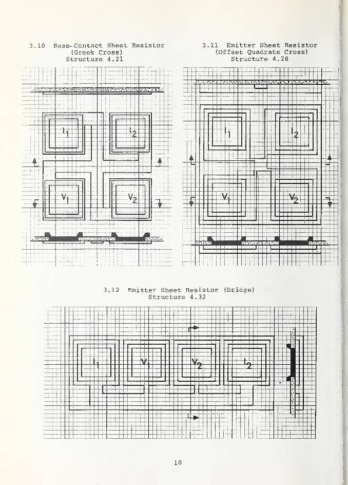
3.10 Base-Contact Sheet Resistor (Greek Cross), Structure 4.21 ... 10
3.11 Emitter Sheet Resistor (Offset Quadrate Cross),Structure 4.28 10
3.12 Emitter Sheet Resistor (Bridge), Structure 4.32 10
3.13 Metal Sheet Resistor (Greek Cross), Structure 4.19 11
3.14 Metal-to-Base Contact Resistor, Structure 4.29 11
3.15 Metal-to-Emitter Contact Resistor, Structure 4.27 . 11
3.16 Collector Four-Probe Resistors, Structures 4.1, 4.5, 4.7,4.9, and 4.17 12
3.17 Collector Hall Effect Device (VDP), Structure 4.31 ...... 13
3.18 Metal Step-Coverage Resistor, Structure 4.38 13
3.19 Collector Spreading Resistor, Structure 4.18 14
MOS Capacitors 15
4.1 MOS Capacitor over Collector (Base DGR, CS) , Structure 4.2 . . 15
4.2 MOS Capacitor over Collector (Emitter DGR), Structure 4.3 . . 16
4.3 MOS Capacitor over Collector (FP, CS), Structure 4.8 17
4.4 MOS Capacitor over Collector, Structure 4.30 17
4.5 MOS Capacitor over Base, Structure 4.12 18
iii
Page
5. Diodes 19
5.1 Base-Collector Diode (FP, CS) , Structure 4.10 19
5.2 Base-Collector Diode (FP, CS) , Structure 4.14 20
6. Transistors 20
6.1 Bipolar Transistor, Structure 4.13 .... 20
6.2 MOS Transistor (Circular), Structure 4.15 21
6.3 MOS Transistor, Structure 4.16 22
7. Miscellaneous 2 3
7.1 Alignment Markers for Negative Photoresist, Structure 4.4 N . .23
7.2 Alignment Markers for Positive Photoresist, Structure 4.4 P . .24
7.3 NBS Logo, Structure 4.6 24
7.4 Surface Profilometer Structure, Structure 4.34 25
7.5 Etch-Control Structures, Structures 4.36 B, E, C, M, BC , G . . 26
7.6 Resolution Structures, Structures 4.37 B, E, C, M, BC , G ... 26
References 27
Appendix 28
LIST OF FIGURES
1. Test pattern NBS-4 fabricated with BASE (B) , EMITTER (E) , BASE-CONTACT (BC) , CONTACT (C) , and METAL (M) masks 3
2. An illustration of the notation used in views of a test structure .5
3. Quadrant 1 of test pattern NBS-4 29
4. BASE mask for quadrant 1 of test pattern NBS-4 31
5. BASE-CONTACT mask for quadrant 1 of test pattern NBS-4 33
6. EMITTER mask for quadrant 1 of test pattern NBS-4 35
7. GATE mask for quadrant 1 of test pattern NBS-4 37
8. CONTACT mask for quadrant 1 of test pattern NBS-4 39
9. METAL mask for quadrant 1 of test pattern NBS-4 41
10. Quadrant 2 of test pattern NBS-4 43
11. BASE mask for quadrant 2 of test pattern NBS-4 45
12. BASE-CONTACT mask for quadrant 2 of test pattern NBS-4 . ." 47
13. EMITTER mask for quadrant 2 of test pattern NBS-4 49
iv

Page
14. GATE mask for quadrant 2 of test pattern NBS-4 51
15. CONTACT mask for quadrant 2 of test pattern NBS-4 53
16. METAL mask for quadrant 2 of test pattern NBS-4 55
17. Quadrant 3 of test pattern NBS-4 57
18. BASE mask for quadrant 3 of test pattern NBS-4 59
19. BASE-CONTACT mask for quadrant 3 of test pattern NBS-4 61
20. EMITTER mask for quadrant 3 of test pattern NBS-4 63
21. GATE mask for quadrant 3 of test pattern NBS-4 65
22. CONTACT mask for quadrant 3 of test pattern NBS-4 67
23. METAL mask for quadrant 3 of test pattern NBS-4 69
24. Quadrant 4 of test pattern NBS-4 71
25. BASE mask for quadrant 4 of test pattern NBS-4 73
26. BASE-CONTACT mask for quadrant 4 of test pattern NBS-4 75
27. EMITTER mask for quadrant 4 of test pattern NBS-4 77
28. GATE mask for quadrant 4 of test pattern NBS-4 79
29. CONTACT mask for quadrant 4 of test pattern NBS-4 81
30. METAL mask for quadrant 4 of test pattern NBS-4 83
LIST OF TABLES
1. Planar Test Structures on Test Pattern NBS-4 2
2. Test Structures Shown in Figures 3-9 28
3. Test Structures Shown in Figures 10-16 42
4. Test Structure Shown in Figures 17-23 56
5. Test Structures Shown in Figures 24-30 70
v

PREFACE
The work was conducted as part of the Semiconductor Technology Program atthe National Bureau of Standards. Portions of this work were supported bythe Defense Advanced Research Projects Agency (Order No. 2 397) and the NBS
.
In the semiconductor industry it is common practice to design photomasks inEnglish units. The photomasks used in this study were laid out in Englishunits. The equivalent metric unit is given in parentheses; in some cases theequivalent is rounded off to an appropriate number of significant figures.
The authors wish to thank several members of the Electronic Technology Divi-sion for their assistance. Y. M. Liu developed the wafer fabrication pro-cesses, W. A. Cullins prepared most of the drawings, Cindy Cannon photo-graphed the wafers and masks, and Jane Walters typed the manuscript.
vi
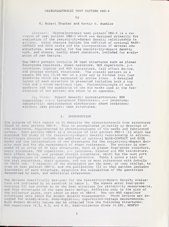
MICROELECTRONIC TEST PATTERN NBS-4
by
W. Robert Thurber and Martin G. Buehler
Abstract: Microelectronic test pattern NBS-4 is a re-vision of test pattern NBS-3 which was designed primarily forevaluation of the resistivity-dopant density relationship insilicon. Major changes include the addition of optional BASE-CONTACT and GATE masks and the incorporation of several newstructures, some useful for the resistivity-dopant densitywork, and others, mostly sheet resistors, included for evalu-ation of new designs.
The NBS-4 pattern contains 38 test structures such as planarfour-probe resistors, sheet resistors, MOS capacitors, p-njunctions, bipolar and MOS transistors, Hall effect device,and process control structures. The overall pattern is asquare 200 mil (5.08 mm) on a side and is divided into fourquadrants which are separated by scribe lines. A detailedlayout of each structure is presented including both a topview and a cross sectional view. Photomicrographs of eachquadrant and the quadrants of the six masks used in the fab-rication of the pattern are shown in an appendix.
Key Words: Dopant density; microelectronics; MOScapacitors; n-p-n transistor fabrication; p-n junctions;resistivity; semiconductor electronics; sheet resistors;silicon; test pattern; test structures.
1. INTRODUCTION
The purpose of this report is to describe the microelectronic test structuresfound on test pattern NBS-4. This is accomplished primarily by drawings ofthe structures, supplemented by photomicrographs of the masks and fabricatedwafers. Test pattern NBS-4 is a revision of test pattern NBS-3 [1] which wasdesigned for study of the resistivity-dopant density relationship in silicon.Significant changes include the addition of optional BASE-CONTACT and GATEmasks and the incorporation of new structures for the resistivity-dopant den-sity work and for the measurement of sheet resistance. The pattern is com-posed of an array of 38 test structures, such as planar four-probe resistors,sheet resistors, MOS capacitors, p-n junctions, bipolar and MOS transistors,Hall effect device, and process control structures, which for the most partare adaptations of commonly used configurations. Table 1 gives a list ofthe test structures, their purpose, and one or more references with detailson their use. A majority of the structures are the same, or very similar, toones on test pattern NBS-3, and the publication [1] on that pattern includesdiscussion of each structure, equations for calculation of the quantitiesdetermined by each, and additional references.
The devices specifically designed for the resistivity-dopant density evalua-tion are indicated by an asterisk in table 1. The square array four-proberesistor [2] has proven to be the best structure for resistivity measurements,and four structures of the same basic design, differing only in the size ofthe collector pipes, were added as part of NBS-4. Two new MOS capacitorstructures were added for dopant density measurements. These devices are de-signed for steady-state, deep-depletion, capacitance-voltage measurements.Bulk dopant density values can be obtained from the following structures:MOS capacitors (4.2, 4.3, and 4.8), base-collector diode (4.10), MOSFET
1

Table 1 - Planar Test Structures on Test Pattern NBS-4
Page NumberTest Structure3 Purpose References
12 4 .1 *Collector resistor (pipes 0.20 mil on Resistivity 1,2a side)
15 4 .2 *MOS capacitor over collector (base DGR) Dopant density 4
16 4 . 3 *MOS capacitor over collector (emitter Dopant density 4
DGR)23,24 4 .4 Alignment markers Mask alignment12 4 . 5 Collector resistor (pipes 0.30 mil on Resistivity 1,2
a side)24 4 .6 Logo Identification12 4 .7 Collector resistor (pipes 0.40 mil on Resistivity 1,2
a side)17 4 . 8 *MOS capacitor over collector (FP, CS) Dopan t den s i ty
,
Vf ,b
1,5
12 4 .9 *Collector resistor (pipes 0.50 mil ontD
Resistivity 1,2a side)
19 4 .10 *Base-collector diode (FP, CS) Dopant density 1,67 4 .11 Base sheet resistor (VDP, FP , CS) Sheet resistance 1,3
18 4 .12 MOS capacitor over base Surface dopant 1
density20 4 .13 Bipolar transistor Proper fabrication 1,720 4 .14 Base-collector diode (FP, CS) Dopant density 1,821 4 .15 *MOSFET (circular, W/L = 18.2) Dopant density 1,922 4 .16 MOSFET (rectangular, W/L = 4) Proper fabrication 1
12 4 .17 *Collector resistor (pipes 0.25 mil on Resistivity 1,2a side)
14 4 .18 Collector spreading resistor Back-side resis- 1,10tance
11 4 .19 Metal sheet resistor (Greek cross) Sheet resistance 1
9 4 . 20 Base-under-emitter sheet resistor Sheet resistance 7,11(Greek cross)
10 4 .21 Base-contact sheet resistor (Greek Sheet resistance 12cross)
6 4 .22 Base sheet resistor (narrow Greek Sheet resistance 3,12cross)
9 4 .23 Base sheet resistor (B, W/L = 0.25) Sheet resistance 7,136 4 .24 Base sheet resistor (Greek cross) Sheet resistance 2 ,126 4 .25 Base sheet resistor (Greek cross, tab Sheet resistance 2,12
contacts)6 4 .26 Base sheet resistor (offset quadrate Sheet resistance 2,12
cross)11 4 .27 Metal-to-emitter contact resistor Contact resistance 1
10 4 .28 Emitter sheet resistor (offset quadrate Sheet resistance 1, 12cross
)
11 4 29 Metal-to-base contact resistor Contact resistance 1
17 4 .30 MOS capacitor over collector (square) Measurement limita- 1
tions13 4 31 *Hall effect device (VDP) Carrier density 1,1410 4 . 32 Emitter sheet resistor (B, W/L = 0.25) Sheet resistance 1
9 4 .33 Base sheet resistor (B, W/L = 0.25) Sheet resistance 1,1325 4 34 Surface profilometer structure Process control 1
8 4 35 Incremental base sheet resistor (VDP) Dopant profile 1,326 4 .36 Etch-control structures0 Process control 1
26 4 .37 Resolution structures 0 Process control 1
13 4 . 38 Metal step-coverage resistor Metal continuity 1
*= structures designed for resistivity-dopant density evaluation.
B = bridge; CS = channel stop; DGR = diffused guard ring; FP = field plate; L = lengthalong current path; VDP = van der Pauw; W = width of current path.
^Vfk = flat band voltage.
CB = BASE mask; BC = BASE-CONTACT mask; C = CONTACT mask; E = EMITTER mask; G = GATEmask; M = METAL mask.
2

Figure 1. Test pattern NBS-4 fabricated with BASE (B) , EMITTER (E) , BASE-CONTACT (BC) , CONTACT (C) , and METAL (M) masks. The length of the pattern
j
along one side is 200 mil (5.08 mm).
3

(4.15), and Hall effect device (4.31). Bulk resistivity values can be foundfrom the square array four-probe collector resistors (4.1, 4.5, 4.7, 4.9, and4.17) and the Hall effect device (4.31). It should be noted that the collec-tor Hall effect device (4.31) is functional only after it has been scribedfrom the wafer and the back-side metal removed. To accommodate this struc-ture, the scribe grid was omitted from the BASE and EMITTER masks and in-cluded on only the CONTACT and GATE masks.
The new pattern also contains eight base sheet resistors, four of which werenot included on test pattern NBS-3. Comparative measurements have been madeon the six van der Pauw base sheet resistors [3]. The base-under-emittersheet resistor (4.20) is a new structure on the pattern. The metal sheet re-sistor (4.19) is of somewhat different design than that on test pattern NBS-3to avoid the problem of burnout due to high current density in narrow connecting arms. The incremental base sheet resistor (4.35) was modified slightlyfrom the one on test pattern NBS-3. The width of the arms near the body wasincreased to minimize arm resistance which is especially important as thestructure is thinned by repeated layer removal. The addition of the base-contact diffusion in the arms further reduces the resistance. Also, the met-al contact pads were enlarged to allow multiple wire bonds. Many of the re-maining test structures are in support of the primary devices. They were in-cluded to provide tests which can assure that proper fabrication steps havebeen followed and aid in diagnosing problems.
A photomicrograph of test pattern NBS-4 is shown in figure 1. The overallpattern is 200 mils (5.08 mm) on a side and is divided into four quadrants.Enlarged views of each quadrant of the fabricated test pattern and the sixmasks are shown in the Appendix. The masks are: BASE, BASE-CONTACT, EMITTERGATE, CONTACT, and METAL. The BASE and BASE-CONTACT masks delineate regionsto be diffused with a conductivity type opposite from the collector substrateand the EMITTER mask delineates regions to be diffused with a conductivitytype the same as the collector substrate. Emitter-diffused regions are moreheavily doped than the collector. The BASE-CONTACT mask is designed to de-lineate heavily doped diffused regions where electrical contacts are made tobase-diffused regions. It is intended for use in the processing of p-typewafers where low resistance contacts to n-type base regions are a problem.With respect to the placement of the alignment markers, the base-contact dif-fusion was designed to follow the base diffusion. However, the diffusions donot have to be done in this order and in the processing sequence used for theresistivity-dopant density study the base-contact diffusion was made follow-ing the emitter diffusion so that the surface dopant density of the base-contact regions was not reduced by any subsequent high-temperature process-ing steps. The BASE-CONTACT mask is generally not used for n-type wafers asaluminum makes good electrical contact to the typical p-type base diffusion.The GATE mask is used whenever a thin, high quality oxide is needed for theMOS devices. During this step, which follows the diffusions, the previousoxide is removed in the areas delineated by the GATE mask and new oxide isgrown
.
4

2 . TEST STRUCTURES
This section discusses the notation used on the drawings of the test struc-tures which follow in sections 3 through 7. The structures are grouped infive major categories: resistors, MOS capacitors, diodes, transistors, andmiscellaneous. The new structures on the pattern were designed using thesame design rules as for test pattern NBS-3 [1]
.
In the following sections both a detailed top view layout and cross sectionalview of each test structure are given. Figure 2 illustrates the scheme used.In the top views and in the horizontal direction for cross sectional views,the distance between grid lines represents 0.50 mil (12.7 um) . In the crosssectional views, metal regions are black and oxide regions are dotted. Alloxide areas are shown with a thickness of one unit above the silicon surfacewith the exception of gate oxide regions which are only a half unit thick.In top views the gate oxide regions are denoted by dashed lines as there isfrequently not a line in the cross sectional view to indicate the boundary ofthe gate oxide. Regions with a base diffusion are clear and indicated by asolid line two units below the silicon surface. Regions with an emitter dif-fusion are clear and indicated by a solid line one unit below the silicon sur-face. Regions with a base-contact diffusion are clear and indicated by asolid line one-half unit below the silicon surface. (In these views a unitis the distance between adjacent grid lines. Also the silicon surface is as-sumed to be flat for the sake of simplicity; the incorporation of silicon in-to the oxide during thermal oxidation has been ignored.)
The following notation is used to define metal contact pads on the top viewof the drawings
:
B = base contact G = gate contact Ii, 1 2 = current contactsC = collector contact S = source contact Vi , V2 = voltage contactsE = emitter contact D = drain contact
Figure 2. An illustration of the notation used in views of a test structure.The emitter diffusion is used for emitter regions of a bipolar transistor,channel stop (CS) regions, and low-resistance contacts to the collector. Thebase diffusion provides both bipolar transistor base regions and MOS transis-tor source-drain regions.
5

3. RESISTORS
3.1 Base Sheet Resistor(Greek Cross)
Structure 4.22
3.3 Base Sheet Resistor(Greek Cross)
Structure 4.25
i
i 1
-j4-
f 222s4
—
[mmmmmim'm
j-jl
— - -
I-
i-
-4r
f?-
h
j—
L
f \h irH
yr
4—!
- - —1
—
t- rr 4t -L--pU-
4-1
—
- H1 i
l-H-
""-j-U1
''
44—i
—
1
—
3.2 Base Sheet Resistor(Greek Cross)
Structure 4.24
4444-1 14-1-1-1-14-i i i
1
1-rr—r^- rr- 1-"
_| i i i i i 4-:± d rt"4—rt ii
r i— i ii — -
;
-|
| |
WEF™™^+ 4- -
: : :+::::+- 4?r4T| ii 1
T-To----
i-4 -
1t T — I 42- 4f.
_44J
\\--\ 1
TTl''"rt"1
llr
11
(====* =gJ (_
i i
.—| l _
_
1
1
—i i
i
i
—44r+71 ITFT 1 — -
(
I.J..1 11 1.UjjII
1—|—[ -~i-r I
h-mmw —— _J
i
1
H r-|
1 4x
— TilWTTTF-44+1
1
1 M 1
1 1
'
1 1 1 1
1
-H-
3.4 Base Sheet B esistor(Offset Quadrate Cross)
Structure 4
.
26
Wrr44+4-4-
i
4
—
M J 1 —1'
1 -+-!
—
~H h—i 1- !—
I
-1—i—1—
1
j-
n 1—H- -- —444 1: 1--t—
4—4-f~H-- rU 44H—t—
•
1—1 1
1 11
\—i—! m= rr-^+n "Ttl'
--4i i
,1 4 r44-- :
:4tf4::-4i2-H--
h-tr±::::+t -44+- -
i
1 1
i—(-,
•
4==i::: ztftii
-J- -U-L -|— j—f—-—u
—
m-44 44-HtH -1- -H-t- -H- .ii—
1
—i
i 1 11
11
i
—j^—j
—j—i—1—j—1
—j-
-
1_
"' i ! 1
j
_1 ,
1
—
-•
1-4 j-MC ^
i
i
1 CM"
i
H 1
— ,| .
— -+ -
i J4MUfr+n +44
_!
6

3 . 5 Base Shee t Resistor (van der Pauw, field plate, channel stop)Structure 4.11
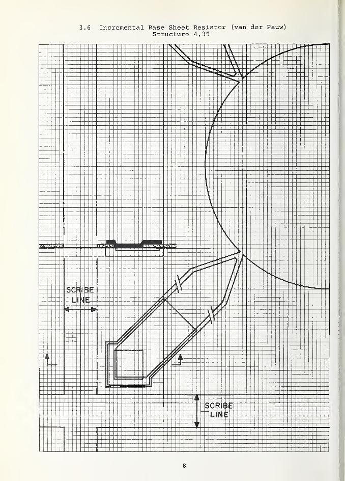
3.6 Incremental Base Sheet Resistor (van der Pauw)Structure 4.35
//
j
1 -
l
—
-4->nHR C
I M IF
h -|
4 \
k
tK:ji
-+.4 H
r
8

3.7 Base Sheet Resistor (Bridge)Structure 4.33
h'-t-H-i i
.i
Ittfc*
"T~H""
I
r:
Vrt i
-i-h- tT
—rtfr M
+4-
ii
!
1 11 1 f 1 1
.i
trri i--[iTt
-f-f-
IP-H-f-
4
-j-hf-i
—
—1—I—i—I—i-- f-+-
H~f4-i-4fff-H-H--i-trt
i— i—r-
t — j—
Base Sheet Resistor 3.9 Base-under-Emitter Sheet Res(Bridge) (Greek Cross)
Structure 4.23 Structure 4.20
3.10 Base-Contact Sheet Resistor(Greek Cross)
Structure 4.21
3.11 Emitter Sheet Resistor(Offset Quadrate Cross)
Structure 4.28
3.12 Emitter Sheet Resistor (Bridge)Structure 4.32
1
-11
t 1 et r
-
1
1 -1
10

3.13 Metal Sheet Resistor(Greek Cross)
Structure 4.19
11

3.16 Collector Four-Probe ResistorsStructure 4.9, pipes 0.50 mil (12.7 um) on a side
X
Other similar structures, which differ primarily in pipe size, are:
Structure 4.1, pipes 0.20 mil (5.1 ym) on a side
Structure 4.5, pipes 0.30 mil (7.5 ym) on a side
Structure 4.7, pipes 0.40 mil (10.2 ym) on a side
Structure 4.17, pipes 0.25 mil (6.4 ym) on a side
12

3.17 Collector Hall Effect Device (van der Pauw)Structure 4.31
U.
m
r
-<
> : r oL i 1 e
C i €
i
3.18 Metal Step-Coverage ResistorStructure 4.38
I
13

3.19 Collector Spreading ResistorStructure 4.18
14

15
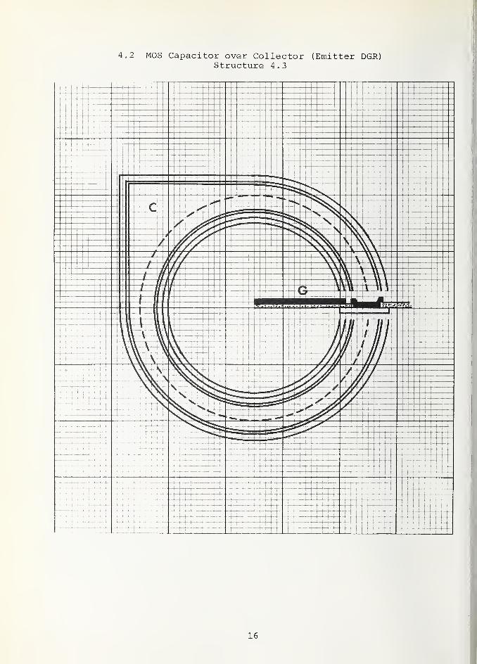
4.2 MOS Capacitor over Collector (Emitter DGR)Structure 4 .
3

4.3 MOS Capacitor over Collector (Field Plate, Channel Stop)Structure 4.8
4.4 MOS Capacitor over CollectorStructure 4.30
17

18

19
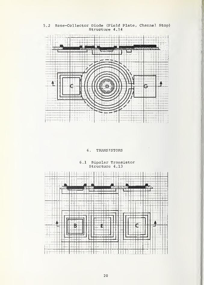
5.2 Base-Collector Diode (Field Plate, Channel Stop)Structure 4.14
6. TRANSISTORS
6.1 Bipolar TransistorStructure 4.13
20

6.2 MOS Transistor (Circular)Structure 4.15
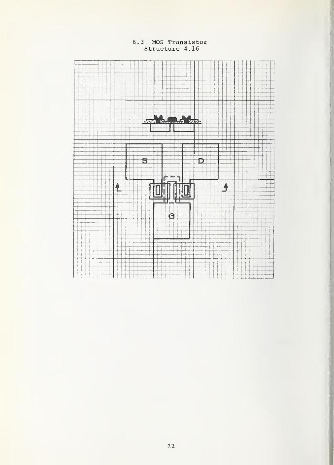
6.3 MOS TransistorStructure 4.16
_l
4
—
4
j—
—j
>Fi
—
*- —
|
1 ;
-r 4 -1:
|
- J_ 4 4-* -4-l .0J
^j
4-i
-4-4
-i- +- — St'as — ~r--4- -4—
h
+--t-
- + —1
r
--f4 -4-f44M-+
i|
-\—\—
i
• -r i
-f
~i-4-
i i
4—-
r -i
1—
^
4-^44!
ii
-4-4--4 -4- - -4
41 tt 4.
44-i-j- -i—
H
-4-4—
-t-+—1—1-
—
h
-i
;44:
ii
tr4 —M~—i—i- 4- - m —j- H-
, i
f~r
~H-——i—
r
-1—t—
t
444444 -4-4-444—1—1-—H-
—H- ttH —(- 4—i-—U-\ M—
f
-i
—-t— i
—
-H-l--H-+ H-
- — —
H
—h++44-
: t-44*+-i
i i
i; i
4-t- -M-i
—
-1-4- j
i i
—I—j
—
44- 1 4 M— _j
—
ff -j-k hi
—
L-i
—
4--—j-
rh~H-t 4 j ! 1
4-—
-
i J±4+4
hi4 —H- -i-
i
'
j—
L
22

7. MISCELLANEOUS
7.1 Alignment Markers for Negative PhotoresistStructure 4.4 N
—._ »
1 t"4
|---
:=\
:=
T ._J ._J
-
LwH. —
p
- -
i-1
'it Ft— F +
-
-
\
- -
>m-i
ft._.
11-i
*This structure will also work with positive photoresist.
23

7.2 Alignment Markers for Positive PhotoresistStructure 4.4 P
j/ c
V! r %b >
\i\ >q tT 1 i —-j
—
i
f IS TJlr J 1 1 #"1
°k41 1 ft
it
-
>U 4 T t p
-\f i
7.3 NBS LogoStructure 4.6
. , , ,
\
1 1 1! !
I |
St! r
-1 4
El 1 r 4 £~ + '
<\\ cO j .J J
_iu -
\- -
ru
L4 i~
imN
n1
r
24
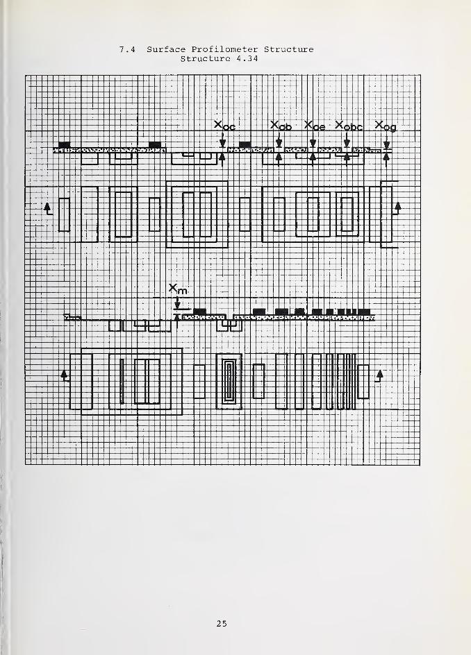
7.4 Surface Profilometer StructureStructure 4.34
25
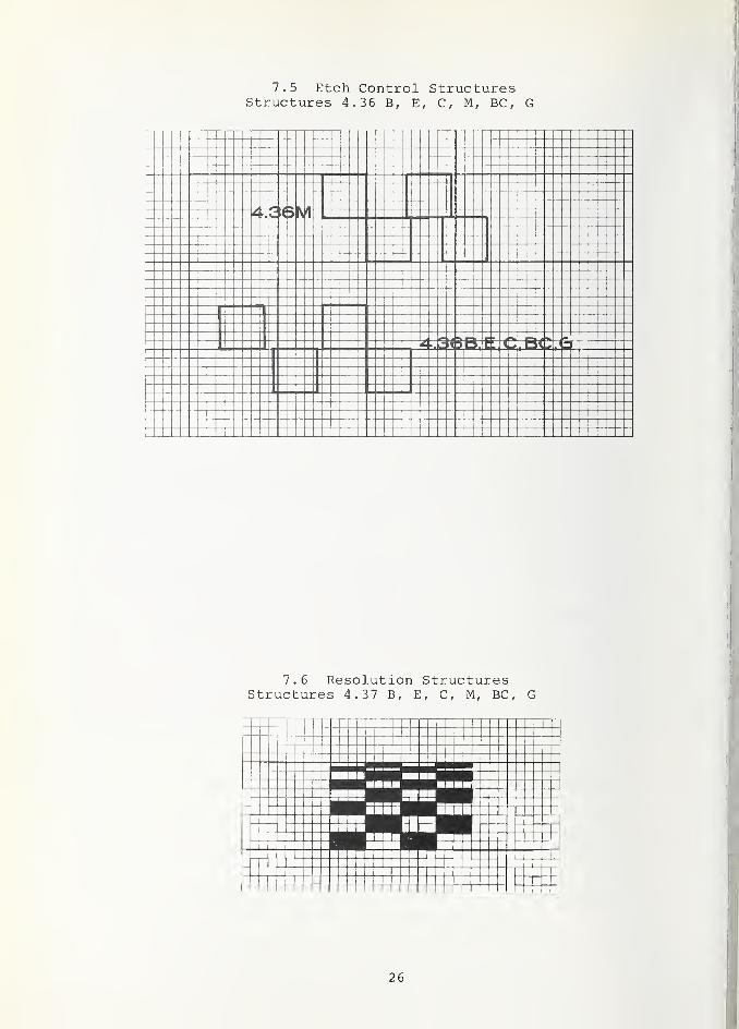
7.5 Etch Control StructuresStructures 4.36 B, E, C, M , BC, G
,£1
i. .t 1
Skm tr t g ,1a :
7.6 Resolution StructuresStructures 4.37 B, E, C, M, BC , G
26

REFERENCES
1. Buehler, M. G. , Semiconductor Measurement Technology: MicroelectronicTest Pattern NBS-3 for Evaluating the Resistivity-Dopant Density Rela-tionship of Silicon, NBS Special Publication 400-22 (May 1976) .
2. Buehler, M. G. , and Thurber, W. R. , A Planar Four-Probe Test Structurefor Measuring Bulk Resistivity, IEEE Trans. Electron Devices ED-23,968-974 (1976)
.
3. Buehler, M. G. , and Thurber, W. R. , An Experimental Study of VariousCross Sheet Resistor Test Structures, J. Electrochem . Soc. 125 , 645-650(1978)
.
4. Brown,. D. M. , Connery, R. J., and Gray, P. V., Doping Profiles by MOSFETDeep Depletion C (V) , J. Electrochem. Soc. 122 , 121-127 (1975).
5. Koyama, R. Y., and Buehler, M. G. , Semiconductor Measurement Technology,W. M. Bullis, Ed., NBS Special Publication 400-17, pp. 8-11,26-27 (No-vember 19 75)
.
6. Mattis, R. L. , and Buehler, M. G. , A New Method for Calculating Back-ground Dopant Density from p-n Junction Capacitance-Voltage Measurements,J. Electrochem. Soc. 124, 1918-1923 (1977).
7. Buehler, M. G. , and Sawyer, D. E., Microelectronic Test Patterns AidProduction of Custom ICs, Circuits Manufacturing No. 2, 45-56(February 1977)
.
8. Buehler, M. G. , David, J. M. , Mattis, R. L., Phillips, W. E., and Thur-ber, W. R. , Semiconductor Measurement Technology: Planar Test Struc-tures for Characterizing Impurities in Silicon, NBS Special Publication400-21 (December 1975)
.
9. Buehler, M. G., Dopant Profiles Determined from Enhancement Mode MOSFETd-c Measurements, Appl. Phys. Letters 3^, 848-850 (1977).
10. Brooks, R. D. , and Mattes, H. G. , Spreading Resistance Between ConstantPotential Surfaces, Bell System Tech. J. 5_0, 775-784 (1971) .
111. Saltich, J. L. , Volk, C. E., and Clark, L. E., Use of Specific EmitterEfficiency in Evaluation and Design of Bipolar Transistors, Proc. IEEE61, 680-681 (1973)
.
12. David, J. M. , and Buehler, M. G. , A Numerical Analysis of Various CrossSheet Resistor Test Structures, Solid-State Electronics 2_0, 539-543(1977).
|l3. Buehler, M. G. , Grant, S. D., and Thurber, W. R. , Bridge and van derPauw Sheet Resistors for Characterizing the Line Width of ConductingLayers, J. Electrochem. Soc. 125 , 650-654 (1978)
.
14. Chwang, R. , Smith, B. J., and Crowell, C. R. , Contact Size Effects onthe van der Pauw Method for Resistivity and Hall Coefficient Measure-ments, Solid-State Electronics 17, 1217-1227 .(1974).
27

APPENDIX
In the following figures, the center-to-center distance between the scribelines is 100 mil (2.54 mm). For all masks except the METAL mask the areasdelineated for subsequent diffusion, oxidation, or oxide removal appear whiin the photomicrographs of the masks. On the METAL mask the metallizationpattern is black on a white background.
Table 2 — Test Structures Shown in Figures 3-9.
Number Test Structure
4.1 Collector resistor (pipes 0.20 mil on a side)
4.2 MOS capacitor over collector (base DGR)
4.3 MOS capacitor over collector (emitter DGR)
4.4 Alignment markers
4.5 Collector resistor (pipes 0.30 mil on a side)
4 . 6 Logo
4.7 Collector resistor (pipes 0.40 mil on a side)
4.8 MOS capacitor over collector (FP, CS)
4.9 Collector resistor (pipes 0.50 mil on a side)
4.10 Base-collector diode (FP, CS)
4.11 Base sheet resistor (VDP, FP , CS)
28

Figure 3. Quadrant 1 of test pattern NBS-4. Test structures are identifiedin table 2.
29


Figure 4. BASE mask for quadrant 1 of test pattern NBS-4. Test structureslocated in this quadrant are listed in table 2.
31

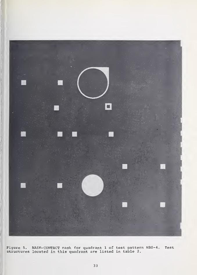
Figure 5. BASE-CONTACT mask for quadrant 1 of test pattern NBS-4. Teststructures located in this quadrant are listed in table 2.
33

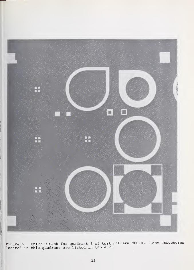
Figure 6. EMITTER mask for quadrant 1 of test pattern NBS-4. Test structures
located in this quadrant are listed in table 2.
35

I


Table 3 — Test Structures Shown in Figures 10-16.
Number Test Structure
4. 12 Mf)^ ranAfi "f~ (~) T~ CWT&T' ]~»^Q^
4. 13 Binol ar tTansi <;f oi*IS -L. _[_ J_ L_. J_ U. 1 1 O _l_ O UV J_
4. 14 Racp-pnl 1 ppfnr H i nH p ("PT>
4. 15 MO^VFT fpirpnlar W/T, = 1 P 1
)
llv ± Hi ± \v_J_J_V_H_Ldl. j VV/J_| — J- O * J
A4 . lb
4. 17 Collector resistor (pipes 0.25 mil on a side)
4. 18 Collector spreading resistor
4. 19 Metal sheet resistor (Greek cross)
4. 20 Base-under-emitter sheet resistor (Greek cross)
4
.
21 Base-contact sheet resistor (Greek cross)
4. 22 Base sheet resistor (narrow Greek cross)
4. 23 Base sheet resistor (bridge, W/L = 0.25)
4. 24 Base sheet resistor (Greek cross)
4. 25 Base sheet resistor (Greek cross, tab contacts)
4. 26 Base sheet resistor (offset quadrate cross)
4. 27 Metal-to-emitter contact resistor
4. 28 Emitter sheet resistor (offset quadrate cross)
4. 29 Metal-to-base contact resistor
4. 30 MOS capacitor over collector (square)
42


1

;
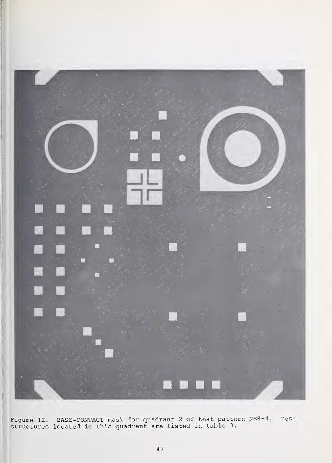
Figure 12. BASE -CONTACT mask for quadrant 2 of test pattern NBS-4. Teststructures located in this quadrant are listed in table 3.
47
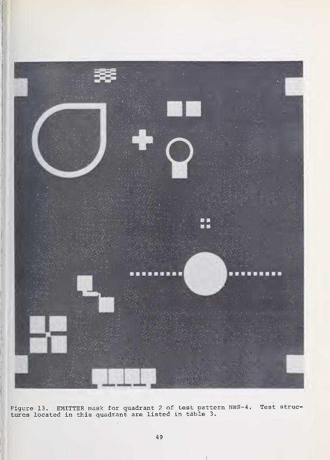
Figure 13. EMITTER mask for quadrant 2 of test pattern NBS-4. Test struc-tures located in this quadrant are listed in table 3.
49


Figure 14. GATE mask for quadrant 2 of test pattern NBS-4. Test structureslocated in this quadrant are listed in table 3.
51
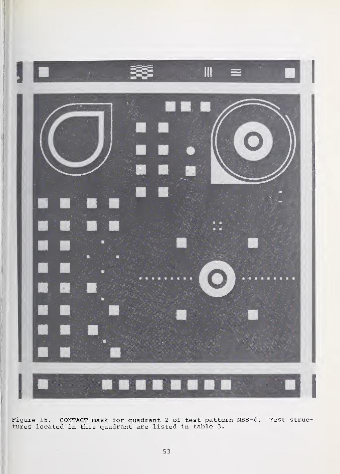
Figure 15. CONTACT mask for quadrant 2 of test pattern NBS-4. Test struc-tures located in this quadrant are listed in table 3.
53

I W ==!= sMJOl
Figure 16. METAL mask for quadrant 2 of test pattern NBS-4. Test structureslocated in this quadrant are listed in table 3.
55
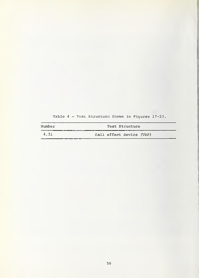
Table 4 — Test Structure Shown in Figures 17-23.
Number Test Structure
4.31 Hall effect device (VDP)
56

Figure 17. Quadrant 3 of test pattern NBS-4. The only test structure inthis quadrant is the Hall effect device listed in table 4.
57

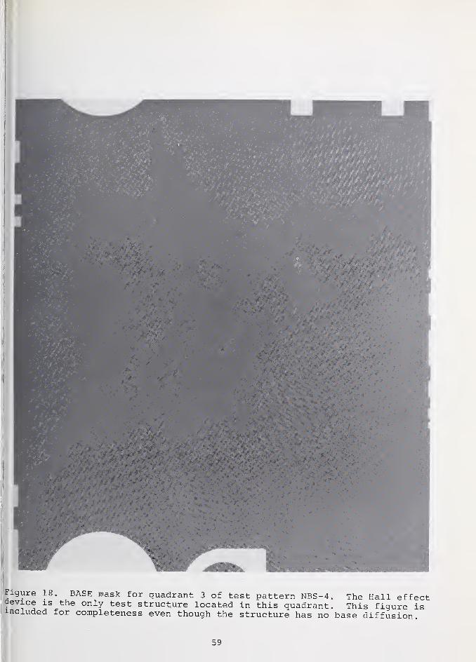
Figure 18. BASE mask for quadrant 3 of test pattern NBS-4. The Hall effectdevice is the only test structure located in this quadrant. This figure isincluded for completeness even though the structure has no base diffusion
59
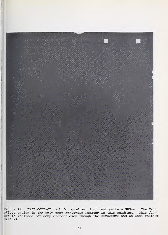
Figure 19. BASE-CONTACT mask for quadrant 3 of test pattern NBS-4. The Halleffect device is the only test structure located in this quadrant. This fig-ure is included for completeness even though the structure has no base contactdiffusion
.
61

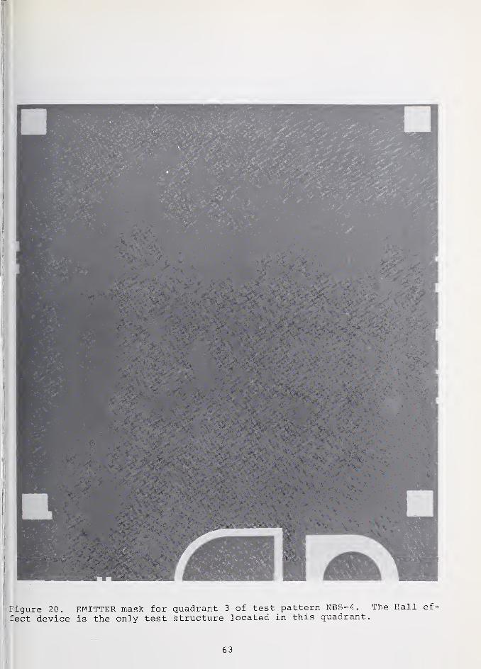


Figure 21. GATE mask for quadrant 3 of test pattern NBS-4 . The Hall effectdevice is the only test structure located in this quadrant. The GATE maskis not involved in the fabrication of this structure, but it does remove ox-ide from the scribe lines surrounding the structure.
65
i
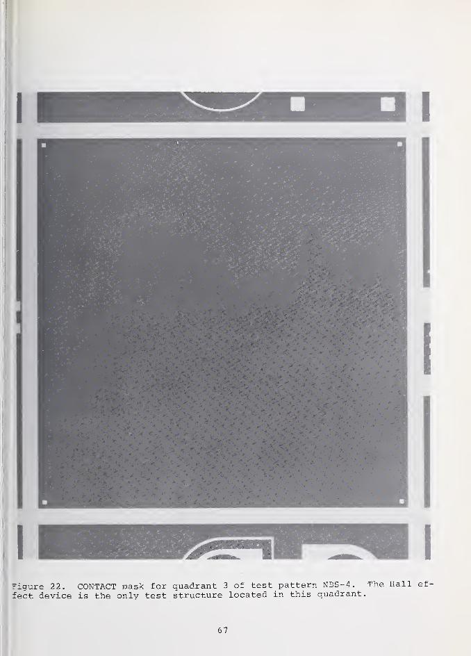
Figure 22. CONTACT mask for quadrant 3 of test pattern NBS-4. The Hallfeet device is the only test structure located in this quadrant.
67

69

Table 5 — Test Structures Shown in Figures 24 -30.
Number Test Structure
4. 32 Emitter sheet resistor (bridge, W/L = 0.25)
4.33 Base sheet resistor (bridge, W/L = 0. 25)
4.34 Surface profilometer structure
4. 35 Incremental base sheet resistor (VDP)
4. 36 Etch-control structures
4. 37 Resolution structures
4.38 Metal step-coverage resistor
70
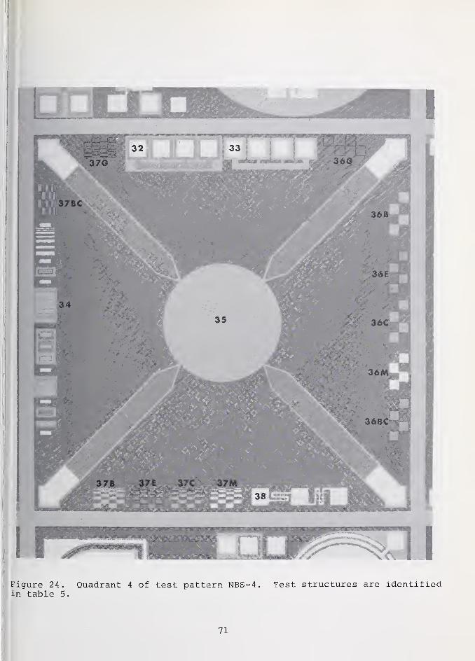
Figure 24. Quadrant 4 of test pattern NBS-4. Test structures are identifiedin table 5.
71

Figure 25. BASE mask for quadrant 4 of test pattern NBS-4. Test structureslocated in this quadrant are listed in table 5.
73


Figure 26. BASE-CONTACT mask for quadrant 4 of test pattern NBS-4. Teststructures located in this quadrant are listed in table 5.
75

i
I
i

Figure 27. EMITTER mask for quadrant 4 of test pattern NBS-4. Test struc-
tures located in this quadrant are listed in table 5.
77

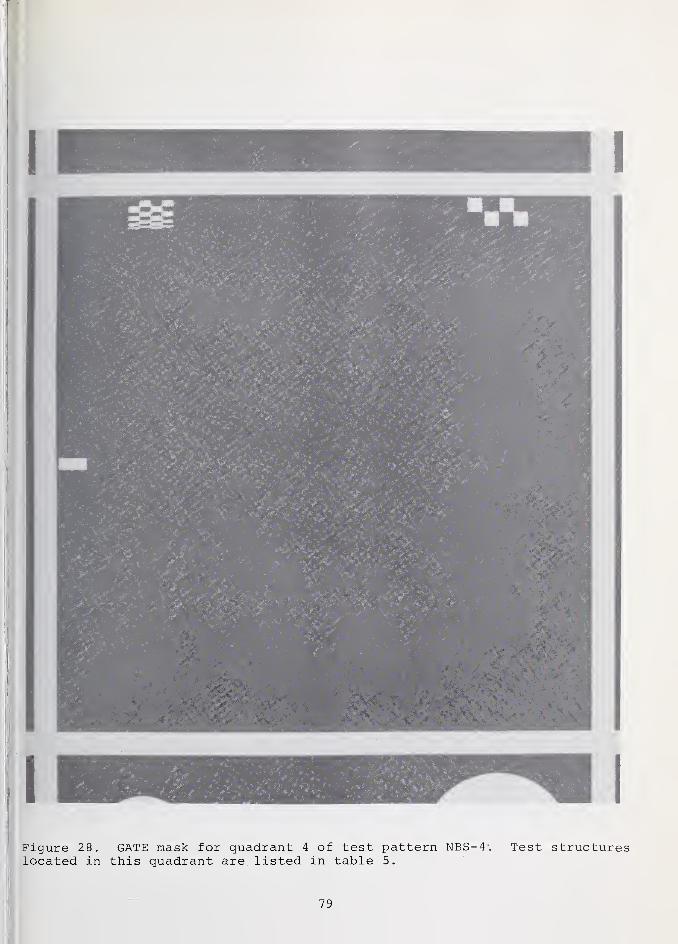
gure 28. GATE mask for quadrant 4 of test pattern NBS-4-. Tecated in this quadrant are listed in table 5.
79
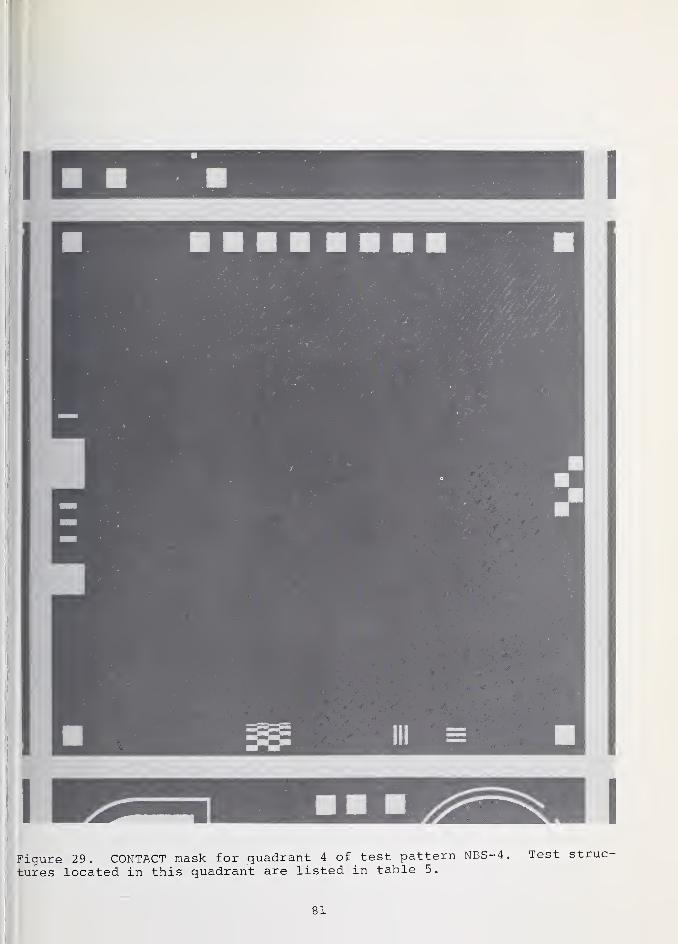
Figure 29. CONTACT mask for quadrant 4 of test pattern NBS-4. Test str
tures located in this quadrant are listed in table 5.
81
t

U. S. GOVERNMENT PRINTING OFFICE : 1978—261-238/56
83


NBS-114A (REV. 7-73)
r U.S. DEPT. OF COMM.
BIBLIOGRAPHIC DATASHEET
1. PUBLICATION OR REPORT NO.
NBS SP-400-32
2. Gov't AccessionNo.
3. Recipient's Accession No.
TITLE AND SUBTITLE
Semiconductor Measurement Technology:
Microelectronic Test Pattern NBS-4
5. Publication Date
April 19786. Performing Organization Code
A UTHOR (S
)
W. Robert Thurber and Martin G. Buehler8. Performing Organ. Report No.
9. PERFORMING ORGANIZATION NAME AND ADDRESS
NATIONAL BUREAU OF STANDARDSDEPARTMENT OF COMMERCEWASHINGTON, D.C. 20234
10. Project/Task/Work Unit No.
425637211. Contract/Grant No.
ARPA Order No. 2397
12. Sponsoring Organization Name and Complete Address (Street, City, State, ZIP)
ARPA - 1400 Wilson Blvd., Arlington, Virginia 22209
NBS - Washington, D. C. 20234
13. Type of Report & PeriodCovered
NBS Spec. Publ
.
14. Sponsoring Agency Code
15. SUPPLEMENTARY NOTES
Library of Congress Catalog Card Number; 78-606024
ljl6. ABSTRACT (A 200-word or less factual summary of most significant information. If document includes a significant
J bibliography or literature survey, mention it here.)
Microelectronic test pattern NBS-4 is a revision of test pattern NBS-3 which
was designed primarily for evaluation of the resistivity-dopant density rela-
tionship in silicon. Major changes include the addition of optional BASE-
CONTACT and GATE masks and the incorporation of several new structures, some
useful for the resistivity-dopant density work, and others, mostly sheet resis-
tors, included for evaluation of new designs.!'
The NBS-4 pattern contains 38 test structures such as planar four-probe resis-11
tors, sheet resistors, M0S capacitors, p-n junctions, bipolar and M0S transis-
tors, Hall effect device, and process control structures. The overall pattern
is a square 200 mil (5.08 mm) on a side and is divided into four quadrants which
are separated by scribe lines. A detailed layout of each structure is presented
including both a top view and a cross sectional view. Photomicrographs of each
quadrant and the quadrants of the six masks used in the fabrication of the pat-
tern are shown in an appendix.
17. KEY WORDS (six to twelve entries; alphabetical order; capitalize only the first letter of the first key word unless a proper
name; separated by semicolons
)
Dopant density; microelectronics; M0S capacitors; n-p-n transistor fabrication; p-n
junctions; resistivity; semiconductor electronics; sheet resistors; silicon; test
pattern; test structures.
18. AVAILABILITY |xH Unlimited
|I For Official Distribution. Do Not Release to NTIS
|"~x! Order From Sup. of Doc, U.S. Government Printing Office
Washington, D.C. 20402, SD Stock No. SN00L-QP3 -
| |Order From National Technical Information Service (NTIS)
Springfield, Virginia 22151
19. SECURITY CLASS(THIS REPORT)
UNCL ASSIFIED
20. SECURITY CLASS(THIS PAGE)
UNCLASSIFIED
21. NO. OF PAGES
66
22. Price
$2.75


NBS TECHNICAL PUBLICATIONS
PERIODICALS
JOURNAL OF RESEARCH—The Journal of Research
of the National Bureau of Standards reports NBS research
and development in those disciplines of the physical and
engineering sciences in which the Bureau is active. These
include physics, chemistry, engineering, mathematics, andcomputer sciences. Papers cover a broad range of subjects,
with major emphasis on measurement methodology, andthe basic technology underlying standardization. Also in-
cluded from time to time are survey articles on topics closely
related to the Bureau's technical and scientific programs. Asa special service to subscribers each issue contains complete
citations to all recent NBS publications in NBS and non-
NBS media. Issued six times a year. Annual subscription:
domestic $17.00; foreign $21.25. Single copy, $3.00 domestic;
$3.75 foreign.
Note: The Journal was formerly published in two sections:
Section A "Physics and Chemistry" and Section B "Mathe-matical Sciences."
DIMENSIONS/NBSThis monthly magazine is published to inform scientists,
engineers, businessmen, industry, teachers, students, andconsumers of the latest advances in science and technology,
with primary emphasis on the work at NBS. The magazinehighlights and reviews such issues as energy research, fire
protection, building technology, metric conversion, pollution
abatement, health and safety, and consumer product per-
formance. In addition, it reports the results of Bureau pro-
grams in measurement standards and techniques, properties
of matter and materials, engineering standards and services,
instrumentation, and automatic data processing.
Annual subscription: Domestic, $12.50; Foreign $15.65.
NONPERIODICALSMonographs—Major contributions to the technical liter-
ature on various subjects related to the Bureau's scientific
and technical activities.
Handbooks—Recommended codes of engineering and indus-
trial practice (including safety codes) developed in coopera-
tion with interested industries, professional organizations,
and regulatory bodies.
Special Publications—Include proceedings of conferences
sponsored by NBS, NBS annual reports, and other special
publications appropriate to this grouping such as wall charts,
pocket cards, and bibliographies.
Applied Mathematics Series—Mathematical tables, man-uals, and studies of special interest to physicists, engineers,
chemists, biologists, mathematicians, computer programmers,and others engaged in scientific and technical work.
National Standard Reference Data Series—Provides quanti-
tative data on the physical and chemical properties of
materials, compiled from the world's literature and critically
evaluated. Developed under a world-wide program co-
ordinated by NBS. Program under authority of National
Standard Data Act (Public Law 90-396).
NOTE: At present the principal publication outlet for these
data is the Journal of Physical and Chemical Reference
Data (JPCRD) published quarterly for NBS by the Ameri-can Chemical Society (ACS) and the American Institute of
Physics (AIP). Subscriptions, reprints, and supplementsavailable from ACS, 1155 Sixteenth St. N.W., Wash., D.C.20056.
Building Science Series—Disseminates technical information
developed at the Bureau on building materials, components,systems, and whole structures. The series presents research
results, test methods, and performance criteria related to the
structural and environmental functions and the durability
and safety characteristics of building elements and systems.
Technical Notes—Studies or reports which are complete in
themselves but restrictive in their treatment of a subject.
Analogous to monographs but not so comprehensive in
scope or definitive in treatment of the subject area. Oftenserve as a vehicle for final reports of work performed at
NBS under the sponsorship of other government agencies.
Voluntary Product Standards—Developed under procedures
published by the Department of Commerce in Part 10,
Title 15, of the Code of Federal Regulations. The purposeof the standards is to establish nationally recognized require-
ments for products, and to provide all concerned interests
with a basis for common understanding of the characteristics
of the products. NBS administers this program as a supple-
ment to the activities of the private sector standardizing
organizations.
Consumer Information Series—Practical information, basedon NBS research and experience, covering areas of interest
to the consumer. Easily understandable language andillustrations provide useful background knowledge for shop-ping in today's technological marketplace.
Order above NBS publications from: Superintendent ofDocuments, Government Printing Office, Washington, D.C.20402.
Order following NBS publications—NBSIR's and F1PS fromthe National Technical Information Services, Springfield,
Va. 22161.
Federal Information Processing Standards Publications
(FIPS PUB)—Publications in this series collectively consti-
tute the Federal Information Processing Standards Register.
Register serves as the official source of information in the
Federal Government regarding standards issued by NBSpursuant to the Federal Property and Administrative Serv-
ices Act of 1949 as amended, Public Law 89-306 (79 Stat.
1127), and as implemented by Executive Order 11717(38 FR 12315, dated May 11, 1973) and Part 6 of Title 15
CFR (Code of Federal Regulations).
NBS Interagency Reports (NBSIR)—A special series ofinterim or final reports on work performed by NBS for
outside sponsors (both government and non-government).
In general, initial distribution is handled by the sponsor;
public distribution is by the National Technical InformationServices (Springfield, Va. 22161) in paper copy or microfiche
form.
BIBLIOGRAPHIC SUBSCRIPTION SERVICES
The following current-awareness and literature-survey bibli-
ographies are issued periodically by the Bureau:Cryogenic Data Center Current Awareness Service. A litera-
ture survey issued biweekly. Annual subscription: Domes-tic, $25.00; Foreign, $30.00.
Liquified Natural Gas. A literature survey issued quarterly.
Annual subscription: $20.00.
Superconducting Devices and Materials. A literature survey
issued quarterly. Annual subscription: $30.00. Send subscrip-
tion orders and remittances for the preceding bibliographic
services to National Bureau of Standards, Cryogenic Data
Center (275.02) Boulder, Colorado 80302.

U.S. DEPARTMENT OF COMMERCENational Bureau of StandardsWashington. D.C. 20234
OFFICIAL BUSINESS
POSTAGE AND FEES PAIOU.S. DEPARTMENT OF COMMERCE
COM-215
Penalty for Private Use, $300
SPECIAL FOURTH-CLASS RATEBOOK


![[James Thurber] Alarms and Diversions](https://static.fdocuments.us/doc/165x107/55cf9bfd550346d033a821f0/james-thurber-alarms-and-diversions.jpg)


