
VCSELs for Analog Applications Arne Alping Ericsson AB A ...
Upload
vuongthuanCategory
view
222download
0
QUALITY & RELIABILITYReliability of Various Size Oxide Aperture VCSELsFirst published in Proceedings of 52nd ECTC
ABSTRACTThis paper presents AOC’s most recent work on 850-nm oxide aperture verticalcavity surface emitting laser (VCSEL) reliability. The VCSELs studied have a range of aperture diameters from about 5 to 20 µm and the reliability effect ofaperture diameter is of principal interest in this paper. Larger apertures generallyexhibit greater reliability. Electrostatic discharge (ESD) sensitivity thresholds ofthe various oxide aperture VCSELs is discussed, again showing dependence ondiameter, with larger being better. Results for humidity exposure are presented.Here we find no aperture size dependence, because none of the tested designsshow significant susceptibility to humidity-induced degradation. It is demonstratedthat, in addition to end-of-life degradation, VCSELs generally exhibit variation of performance characteristics during the early part of operating life. This oftenleads to a requirement for device burn-in. AOC’s work in the area of waferstabilization (trademarked under the name STABILAZE, patent pending) is intro-duced, showing how critical device parameters such as threshold and slopeefficiency can be made to be unvarying over the product’s life without the needfor costly component or module-level burn-ins.
INTRODUCTION
Following the initial indications that reliable oxide-aperture VCSELs are possible[1,2,3], they represent a growing fraction of all VCSELs produced. As they enterinto more applications, each potentially requiring different design optimization,it becomes important to explore the edges of the islands of reliability. Not everypossible design is equally reliable, and we don’t want to wade so far off shorethat we drown.
The reliability methodology, philosophy, and caveats described in earlier VCSELstudies [1,4,5,6] are similar here; their importance warrants repeating the mostimportant points. For example, extrapolation to failure is unwise for VCSELs,testing at application conditions as well as highly accelerated conditions isrecommended, and it is important to account for wafer and lot variation. Someresults from this work may be generally applicable for all oxide-aperture VCSELs,but the characterization and reliability testing described is specifically for AOCdevices. Our very limited testing of VCSELs of different manufacture shows awide range of reliability performance.
Reliability can have multiple definitions, and there is no singlemeasure that can describe them all. In some cases what wemean by reliability is not how long the devices will last whenoperated as expected, but how long they will last when theunexpected occurs. ESD (and its cousin, electrical overstress,or EOS) and humidity exposure are in this category. Thewearout lifetime that is the more typical subject of reliabilitystudies is of a different character entirely; by either measureAOC VCSELs prove robust. From first principles it is clear thatthey cannot all be equally so, so a range of devices have beentested, with results summarized below. Reliability distributionsand acceleration models are formulated for the various sizesof oxide aperture VCSELs, similar to our previous publicationsfor proton-implanted VCSELs. These allow computation ofexpected reliability at conditions other than the necessarilyaccelerated test environments.
It is to be expected that VCSELs of different designs anddifferent aperture diameters should exhibit different reliability.As we show below, depending on what is considered the mostimportant operating characteristic, the results may not alwaysbe intuitive.
Since device death is not a necessary component of everydefinition of reliability, simple stabilization of operatingcharacteristics can often be just as important, a point oftenoverlooked. This is a critical point for many array products,where stabilized wafers allow for confident selection of arraysat wafer level, without the deleterious increase of non-uniformity during product use.
OXIDE VCSEL DESIGN: EFFECTS AND TRADEOFFS
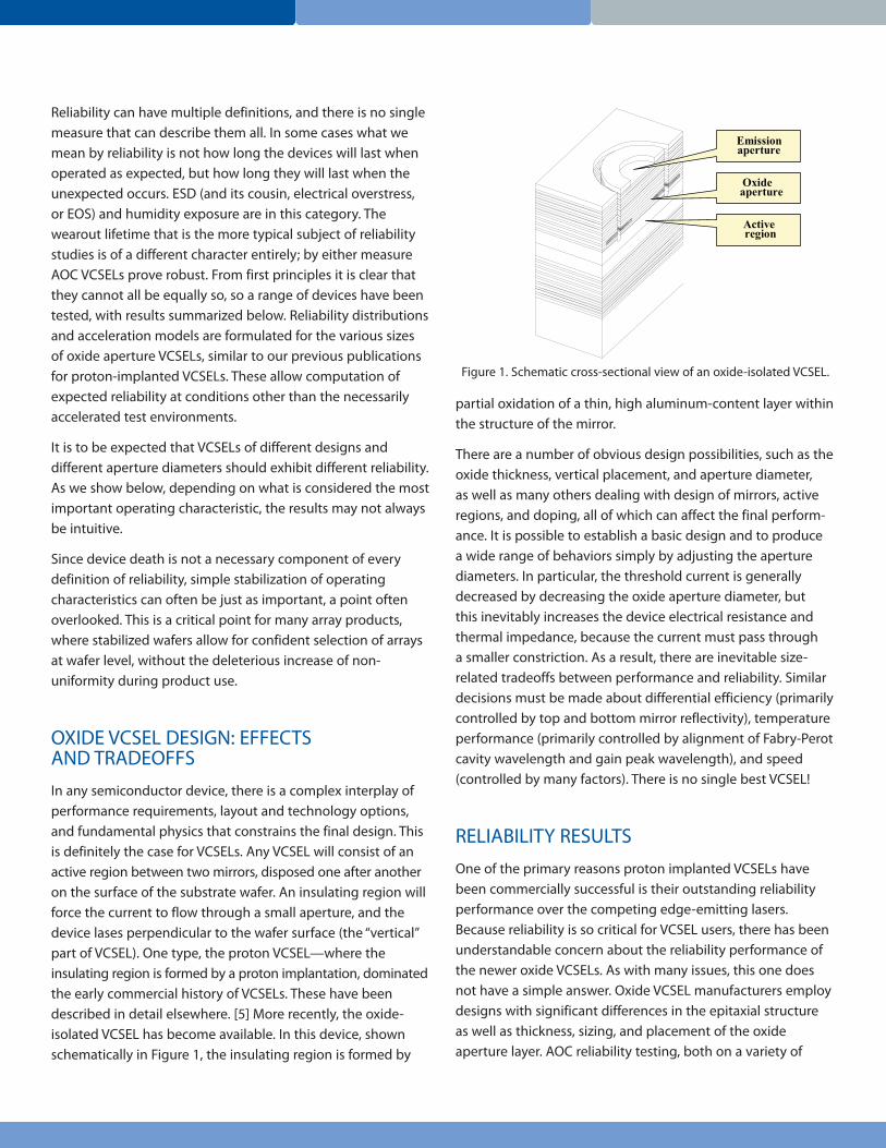
In any semiconductor device, there is a complex interplay ofperformance requirements, layout and technology options,and fundamental physics that constrains the final design. Thisis definitely the case for VCSELs. Any VCSEL will consist of anactive region between two mirrors, disposed one after anotheron the surface of the substrate wafer. An insulating region willforce the current to flow through a small aperture, and thedevice lases perpendicular to the wafer surface (the “vertical”part of VCSEL). One type, the proton VCSEL—where theinsulating region is formed by a proton implantation, dominatedthe early commercial history of VCSELs. These have beendescribed in detail elsewhere. [5] More recently, the oxide-isolated VCSEL has become available. In this device, shownschematically in Figure 1, the insulating region is formed by
partial oxidation of a thin, high aluminum-content layer withinthe structure of the mirror.
There are a number of obvious design possibilities, such as theoxide thickness, vertical placement, and aperture diameter, as well as many others dealing with design of mirrors, activeregions, and doping, all of which can affect the final perform-ance. It is possible to establish a basic design and to produce a wide range of behaviors simply by adjusting the aperturediameters. In particular, the threshold current is generallydecreased by decreasing the oxide aperture diameter, but this inevitably increases the device electrical resistance andthermal impedance, because the current must pass through a smaller constriction. As a result, there are inevitable size-related tradeoffs between performance and reliability. Similardecisions must be made about differential efficiency (primarilycontrolled by top and bottom mirror reflectivity), temperatureperformance (primarily controlled by alignment of Fabry-Perotcavity wavelength and gain peak wavelength), and speed(controlled by many factors). There is no single best VCSEL!
RELIABILITY RESULTS
One of the primary reasons proton implanted VCSELs havebeen commercially successful is their outstanding reliabilityperformance over the competing edge-emitting lasers.Because reliability is so critical for VCSEL users, there has beenunderstandable concern about the reliability performance ofthe newer oxide VCSELs. As with many issues, this one doesnot have a simple answer. Oxide VCSEL manufacturers employdesigns with significant differences in the epitaxial structureas well as thickness, sizing, and placement of the oxideaperture layer. AOC reliability testing, both on a variety of
Emission aperture
Oxide aperture
Active region
Figure 1. Schematic cross-sectional view of an oxide-isolated VCSEL.
internal designs and on competitive products, hasdemonstrated a wide range of reliability results for differentoxide VCSEL designs. These differences can affect reliabilityeither by changing the magnitude of the effect of failuremodes, or by introducing new ones, such as mechanical stressdue to shrinkage on oxidation and to differential thermalexpansion of the oxide relative to the semiconductor material.Failure modes such as these can be insidious, as they may notbe seen in high-temperature life tests. [1] For these reasons,oxide VCSEL reliability must be assessed for each particularoxide design, and the reliability effects of design choices mustbe understood through extensive reliability testing.
As with proton VCSELs, AOC continues to emphasize reliabilityperformance for its oxide VCSEL products. By systematicallytesting numerous design options through statisticalexperimentation techniques, we understand the reliabilityimpact of such choices. Beyond life tests of the type describedhere, AOC continues its reliability process monitoringprotocols. These include qualifying each wafer for productionuse by assessing its parametric stability and long-termreliability through sample life testing, as well as quarterlylong-term life testing of a sample from production stock.VCSEL users also validate reliability of the AOC VCSELproducts (oxide and proton VCSELs); overall VCSEL reliabilityfailures (defined as field failures of any age reported by ourcustomers) were at a 1.3 PPM (6.2 sigma) level for 2001,improved over the 2 PPM reported in 2000. [1]
The reliability results reported here describe the effects of oneof the possible design decisions—aperture diameter. Asmentioned earlier, each choice may be suitable for aparticular application, so there is not necessarily one "best"option. Here we describe the data to assess the reliabilitytrade-offs for each product. Note that reliability discussed inthis section means device wear-out, or lifetime. Short-termreliability effects are dominated by changes (increase ordecrease) in device characteristics, and thus the need fordevice stabilization—an important topic discussed later. Aswas the case for AOC's proton VCSEL, we did not see infantmortality or random failure rates of significance during thistesting.
The life testing methodology is the same as AOC hasdescribed many times before. [6] Multiple wafers representingseveral epitaxial growth and chip fabrication lots wereemployed in the study—at least 3 lots for each chip type.Chips were packaged in TO-style devices, subjected tostandard production burn-in, and then placed on long-term
life testing. Some of the groups were subjected to air-to-airthermal shocks before starting life testing (this did not impactthe results). The burn-in was done in dark, forced-air ovens atabout ten different combinations of constant temperatureand dc current. Periodically the parts were removed from theoven and dc tested at room temperature. As usual, failure isdefined as a 2 dB reduction in output power at a fixed current.While the VCSELs usually degraded in a fairly graceful wayduring life testing (as opposed to sudden, catastrophicdegradation), we did not attempt to estimate extrapolatedfailure times; reported failure times are always for actualfailures.
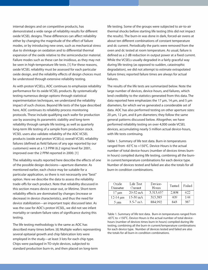
The results of the life tests are summarized below. Note thelarge number of devices, device-hours, and failures, whichlend credibility to the statistics generated from this data. Thedata reported here emphasizes the 17 µm, 14 µm, and 5 µmdiameters, for which we've generated a considerable set ofdata. AOC has also performed testing on other aperture sizes:20 µm, 12 µm, and 8 µm diameters; they follow the samegeneral patterns discussed below. Altogether, we haveperformed reliability testing on over 4,000 oxide VCSELdevices, accumulating nearly 5 million actual device-hours,with life tests continuing.
Table 1. Summary of life test data. Burn-in temperaturesranged from -65°C to +150°C. Device-Hours is the actualnumber of total device-hours (number of devices times burn-in hours) compiled during life testing, combining all the burn-in current/temperature combinations for each device type.Number of devices tested and failed are also the totals for allburn-in condition combinations.
Table 1. Summary of life test data. Burn-in temperatures ranged from-65°C to +150°C. Device-Hours is the actual number of total device-hours (number of devices times burn-in hours) compiled during lifetesting, combining all the burn-in current/temperature combinationsfor each device type. Number of devices tested and failed are alsothe totals for all burn-in condition combinations.
FAILURE MECHANISMS
Data for each of the groups fit the same fundamentaltemperature and current acceleration model we havepublished previously for our proton VCSELs [4]: an Arrheniusmodel with an activation energy of 0.7 eV and an additionaldependence on the square of the applied current. That thesame activation energy applies would be consistent with asingle dominant failure mechanism (or combination of failuremechanisms) for all aperture sizes of our oxide VCSEL as well asfor our proton VCSEL. (Other investigators also subsequentlyfound this activation energy and current-squared dependenceto be the appropriate wearout acceleration model for oxideVCSELs. [16,17])
The ultimate failure mechanism in all cases (both for the oxideand the proton VCSEL) is most likely related to the presenceor generation of dislocations. Edge dislocations that traversethe P-N junction move only as continuous loops by glide orclimb along fixed crystallographic directions and form darkline defects (DLDs) by generating a high density of deep point defect traps along their path of motion. DLDs are darkbecause of the compensating and lifetime killing propertiesof the deep traps. (While it remains true that DLDs of classicalappearance—and resulting rapid degradation—are not foundin AOC VCSELs, these and the following comments contrastwith earlier AOC interpretations. [1,4,5,6] The DLD wearoutmechanism and the stabilization model to be discussedbelow have similar activation energies, but recent careful TEManalysis suggests that dislocations actually control end of life.It remains possible, however, that both mechanisms areeffective at the 2 dB degradation level which is a typicalfailure criterion.)
The laminar structure of the AOC VCSEL confines propagatingdislocations entirely to the plane of the active region(quantum wells and barriers). As a result, the only orientationin which they would appear linear is parallel to the activeplane—in which orientation there would be no illuminatedregion to contrast with the DLD. From the top, the onlydirection in which the degradation can practicably beobserved, the VCSEL emission appears either to dim gradually,progressing inward from an edge, or to dim nearly uniformlyover the entire area. Neither of these conditions is clearlyevident at the 2-dB degradation we use as our end-of-lifedefinition, probably because only a tiny fraction of the outeredge of the active area is involved at that point. They typically
become visible only at 90% or greater degradation. It isprobably this fact that leads to the remarkable reliabilityobserved in the VCSEL ac characteristics. [4]
Two items are absolutely required for the propagation of aDLD: a dislocation (or surface) traversing the junction andmechanical stress. As a practical matter, minority carriers mustalso be present. Without minority carriers, the activation energyfor DLD motion is enormously increased. [7] If any one ofthese three items is missing there will not be DLD degradation.Some mechanical stress is inevitable in the VCSEL; even if not present as a residue of processing, stress will arise fromthermal gradients induced by operation. Minority carriers arealso inescapable consequences of operation.
Dislocations can come from a variety of sources. VCSELmaterial growth by MOCVD employs low dislocation densitysubstrates, but the dislocation density is not zero and a smallbut finite possibility always exists that a substrate dislocationwill traverse the P-N junction inside the diameter of theisolation implant. The central portion of the cavity is the mostvulnerable. Substrate dislocations in the region under theoxide or gain guide implant will have a reduced effect due to the lateral debiasing. Even if a pre-existing dislocation orsurface is not accessible in the region of flowing current, theycan be generated in situ. Point defects can be generated nearthe oxidation layer, and the isolation implant produces a highdensity of point defects that define the perimeter of the P-Njunction. Under forward bias, minority carriers that recombinenon-radiatively on these point defects impart energy to thedefects that allow them to move so as to lower the freeenergy in the crystal. Aggregation of point defects into adislocation loop produces a nucleus for DLD propagation and subsequent degradation.
Degradation resulting from grown-in dislocations is generallyfairly rapid. In the rare instances where it occurs, it cantypically be detected and removed by a short operating burn-in (such as the STABILAZE process described below).Generation of dislocations through aggregation of pointdefects is much slower; it is this mechanism that likelycontrols wearout life of AOC VCSELs. While details of VCSELdegradation remain open issues, it involves a combination ofthe mechanisms above (and perhaps others), and appears tobe fundamentally similar for AOC’s proton and oxide VCSELsof all sizes.
RELIABILITY MODEL
Modeling the cumulative failure rate with time results in acurve best fit by the lognormal distribution, as we haveconsistently reported for the proton and oxide VCSEL [1], seereference [6] for a more complete discussion of the lognormaldistribution. This distribution is often used to model wearout;contrast that with random failures, typically modeled with anexponential distribution. As in our previous studies we do notsee infant mortality or random failures as significant portionsof the time-to-failure distribution, we see only a singlewearout curve.
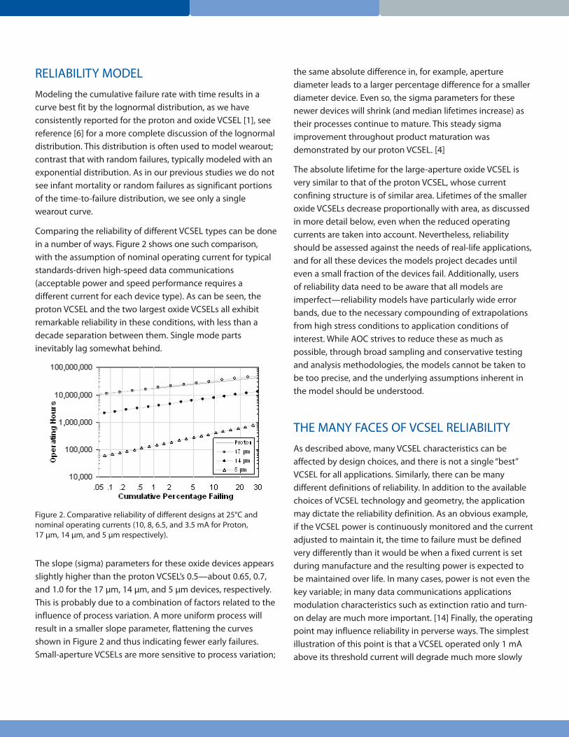
Comparing the reliability of different VCSEL types can be donein a number of ways. Figure 2 shows one such comparison,with the assumption of nominal operating current for typicalstandards-driven high-speed data communications(acceptable power and speed performance requires adifferent current for each device type). As can be seen, theproton VCSEL and the two largest oxide VCSELs all exhibitremarkable reliability in these conditions, with less than adecade separation between them. Single mode partsinevitably lag somewhat behind.
The slope (sigma) parameters for these oxide devices appearsslightly higher than the proton VCSEL’s 0.5—about 0.65, 0.7,and 1.0 for the 17 µm, 14 µm, and 5 µm devices, respectively.This is probably due to a combination of factors related to theinfluence of process variation. A more uniform process willresult in a smaller slope parameter, flattening the curvesshown in Figure 2 and thus indicating fewer early failures.Small-aperture VCSELs are more sensitive to process variation;
the same absolute difference in, for example, aperturediameter leads to a larger percentage difference for a smallerdiameter device. Even so, the sigma parameters for thesenewer devices will shrink (and median lifetimes increase) astheir processes continue to mature. This steady sigmaimprovement throughout product maturation wasdemonstrated by our proton VCSEL. [4]
The absolute lifetime for the large-aperture oxide VCSEL isvery similar to that of the proton VCSEL, whose currentconfining structure is of similar area. Lifetimes of the smalleroxide VCSELs decrease proportionally with area, as discussedin more detail below, even when the reduced operatingcurrents are taken into account. Nevertheless, reliabilityshould be assessed against the needs of real-life applications,and for all these devices the models project decades untileven a small fraction of the devices fail. Additionally, users of reliability data need to be aware that all models areimperfect—reliability models have particularly wide errorbands, due to the necessary compounding of extrapolationsfrom high stress conditions to application conditions ofinterest. While AOC strives to reduce these as much aspossible, through broad sampling and conservative testingand analysis methodologies, the models cannot be taken tobe too precise, and the underlying assumptions inherent inthe model should be understood.
THE MANY FACES OF VCSEL RELIABILITY
As described above, many VCSEL characteristics can beaffected by design choices, and there is not a single “best”VCSEL for all applications. Similarly, there can be manydifferent definitions of reliability. In addition to the availablechoices of VCSEL technology and geometry, the applicationmay dictate the reliability definition. As an obvious example, if the VCSEL power is continuously monitored and the currentadjusted to maintain it, the time to failure must be definedvery differently than it would be when a fixed current is setduring manufacture and the resulting power is expected tobe maintained over life. In many cases, power is not even thekey variable; in many data communications applicationsmodulation characteristics such as extinction ratio and turn-on delay are much more important. [14] Finally, the operatingpoint may influence reliability in perverse ways. The simplestillustration of this point is that a VCSEL operated only 1 mAabove its threshold current will degrade much more slowly
Figure 2. Comparative reliability of different designs at 25°C andnominal operating currents (10, 8, 6.5, and 3.5 mA for Proton, 17 µm, 14 µm, and 5 µm respectively).
than the same device operated 10 mA above its threshold.However, the power effect of a degradation-inducedthreshold increase of 0.9 mA is less than 10% in the lattercase, but it is 90% in the former!
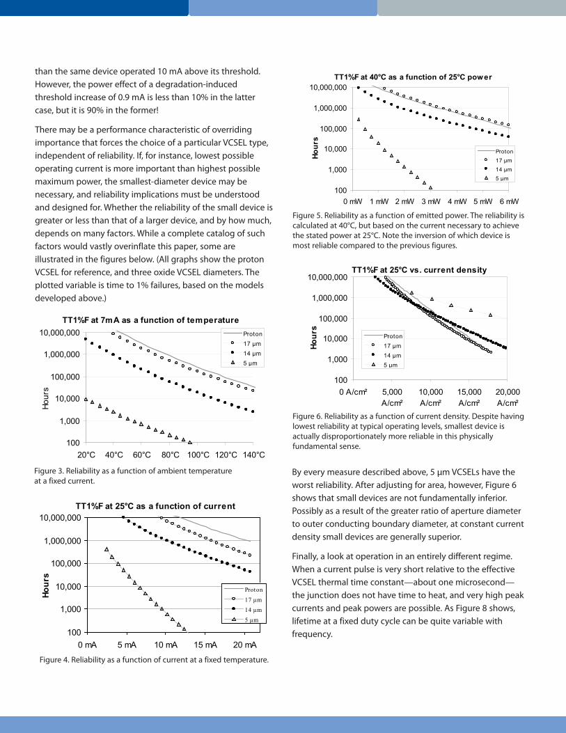
There may be a performance characteristic of overridingimportance that forces the choice of a particular VCSEL type,independent of reliability. If, for instance, lowest possibleoperating current is more important than highest possiblemaximum power, the smallest-diameter device may benecessary, and reliability implications must be understoodand designed for. Whether the reliability of the small device isgreater or less than that of a larger device, and by how much,depends on many factors. While a complete catalog of suchfactors would vastly overinflate this paper, some areillustrated in the figures below. (All graphs show the protonVCSEL for reference, and three oxide VCSEL diameters. Theplotted variable is time to 1% failures, based on the modelsdeveloped above.)
By every measure described above, 5 µm VCSELs have theworst reliability. After adjusting for area, however, Figure 6shows that small devices are not fundamentally inferior.Possibly as a result of the greater ratio of aperture diameter to outer conducting boundary diameter, at constant currentdensity small devices are generally superior.
Finally, a look at operation in an entirely different regime.When a current pulse is very short relative to the effectiveVCSEL thermal time constant—about one microsecond—the junction does not have time to heat, and very high peakcurrents and peak powers are possible. As Figure 8 shows,lifetime at a fixed duty cycle can be quite variable withfrequency.
TT1%F at 7mA as a function of temperature
100
1,000
10,000
100,000
1,000,000
10,000,000
20°C 40°C 60°C 80°C 100°C 120°C 140°C
Hour
s
Proton17 µm14 µm5 µm
Figure 3. Reliability as a function of ambient temperature at a fixed current.
Proton17 µm14 µm5 µm
Figure 4. Reliability as a function of current at a fixed temperature.
TT1%F at 40°C as a function of 25°C power
100
1,000
10,000
100,000
1,000,000
10,000,000
0 mW 1 mW 2 mW 3 mW 4 mW 5 mW 6 mW
Hour
s
Proton17 µm14 µm5 µm
Figure 5. Reliability as a function of emitted power. The reliability iscalculated at 40°C, but based on the current necessary to achievethe stated power at 25°C. Note the inversion of which device is most reliable compared to the previous figures.
TT1%F at 25°C vs. current density
100
1,000
10,000
100,000
1,000,000
10,000,000
0 A/cm² 5,000A/cm²
10,000A/cm²
15,000A/cm²
20,000A/cm²
Hour
s
Proton17 µm14 µm5 µm
Figure 6. Reliability as a function of current density. Despite havinglowest reliability at typical operating levels, smallest device is actually disproportionately more reliable in this physicallyfundamental sense.
HUMIDITY EFFECTS
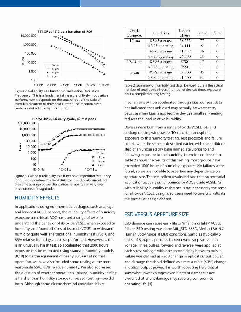
In applications using non-hermetic packages, such as arraysand low-cost VCSEL sensors, the reliability effects of humidityexposure are critical. AOC has used a range of tests tounderstand the behavior of its oxide VCSEL when exposed tohumidity, and found all sizes of its oxide VCSEL to withstandhumidity quite well. The traditional humidity test is 85ºC and85% relative humidity, a test we performed. However, as thisis an unusually harsh test, so accelerated that 2000 hoursexposure can be estimated using standard humidity models[8,18] to be the equivalent of nearly 30 years at normaloperation, we have also included some testing at the morereasonable 65ºC, 65% relative humidity. We also addressedthe question of whether operational (biased) humidity testingis harsher than humidity storage (unbiased) testing—we didboth. Although some electrochemical corrosion failure
mechanisms will be accelerated through bias, our past datahas indicated that unbiased may actually be worst case,because when bias is applied the device’s small self-heatingreduces the local relative humidity.
Devices were built from a range of oxide VCSEL lots andpackaged using windowless TO cans for atmosphericexposure to this humidity testing. Test protocols and failurecriteria were the same as described earlier, with the additionalstep of an unbiased dry bake immediately prior to andfollowing exposure to the humidity, to avoid condensation.Table 2 shows the results of this testing; most groups haveexceeded 1000 hours of humidity exposure. No failures werefound, so we are not able to ascertain any dependence onaperture size. These excellent results indicate that no terrestrialapplication appears out of bounds for AOC’s oxide VCSEL. Aswith reliability, humidity resistance is not necessarily the samefor all oxide VCSEL designs, so users need to carefully validatethe particular design chosen.
ESD VERSUS APERTURE SIZE
ESD damage can cause early life or “infant mortality” VCSELfailure. ESD testing was done MIL_STD-883D, Method 3015.7Human Body Model (HBM) conditions. Samples (typically 5units) of 5-20µm aperture diameter were step stressed involtage. Three pulses, forward and reverse, were applied ateach stress voltage, with one second delay between pulses.Failure was defined as –2dB change in optical output power,and damage threshold defined as a measurable (>3%) changein optical output power. It is worth repeating here that atsomewhat lower voltages even if patent damage is notevident that latent damage may severely compromiseoperating life. [4]
TT1%F at 40°C as a function of ROF
100
1,000
10,000
100,000
1,000,000
10,000,000
0 GHz 2 GHz 4 GHz 6 GHz 8 GHz 10 GHz
Hour
s
Proton17 µm14 µm5 µm
Figure 7. Reliability as a function of Relaxation OscillationFrequency. This is a fundamental measure of likely modulationperformance; it depends on the square root of the ratio ofstimulated current to threshold current. The medium-sized oxide is most reliable by this metric.
TT1%F 40°C, 5% duty cycle, 40 mA peak
10
100
1,000
10,000
100,000
1,000,000
10,000,000
100,000,000
1E+3 Hz 1E+5 Hz 1E+7 Hz
Hour
s
Proton17 µm14 µm5 µm
Figure 8. Calendar reliability as a function of repetition frequencyfor pulsed operation at a fixed duty cycle and peak current. For the same average power dissipation, reliability can vary over three orders of magnitude.
Table 2. Summary of humidity test data. Device-Hours is the actualnumber of total device-hours (number of devices times exposurehours) compiled during testing.
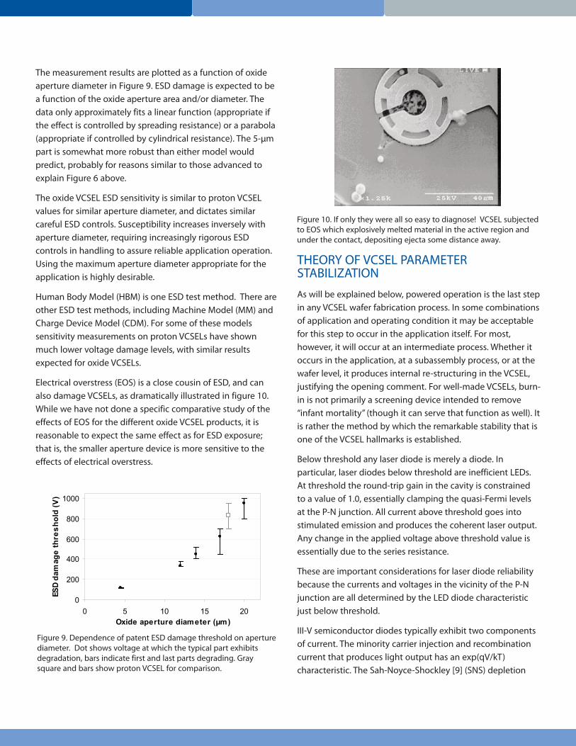
The measurement results are plotted as a function of oxideaperture diameter in Figure 9. ESD damage is expected to bea function of the oxide aperture area and/or diameter. Thedata only approximately fits a linear function (appropriate ifthe effect is controlled by spreading resistance) or a parabola(appropriate if controlled by cylindrical resistance). The 5-µmpart is somewhat more robust than either model wouldpredict, probably for reasons similar to those advanced toexplain Figure 6 above.
The oxide VCSEL ESD sensitivity is similar to proton VCSELvalues for similar aperture diameter, and dictates similarcareful ESD controls. Susceptibility increases inversely withaperture diameter, requiring increasingly rigorous ESDcontrols in handling to assure reliable application operation.Using the maximum aperture diameter appropriate for theapplication is highly desirable.
Human Body Model (HBM) is one ESD test method. There areother ESD test methods, including Machine Model (MM) andCharge Device Model (CDM). For some of these modelssensitivity measurements on proton VCSELs have shownmuch lower voltage damage levels, with similar resultsexpected for oxide VCSELs.
Electrical overstress (EOS) is a close cousin of ESD, and canalso damage VCSELs, as dramatically illustrated in figure 10.While we have not done a specific comparative study of theeffects of EOS for the different oxide VCSEL products, it isreasonable to expect the same effect as for ESD exposure;that is, the smaller aperture device is more sensitive to theeffects of electrical overstress.
THEORY OF VCSEL PARAMETERSTABILIZATION
As will be explained below, powered operation is the last stepin any VCSEL wafer fabrication process. In some combinationsof application and operating condition it may be acceptablefor this step to occur in the application itself. For most,however, it will occur at an intermediate process. Whether itoccurs in the application, at a subassembly process, or at thewafer level, it produces internal re-structuring in the VCSEL,justifying the opening comment. For well-made VCSELs, burn-in is not primarily a screening device intended to remove“infant mortality” (though it can serve that function as well). Itis rather the method by which the remarkable stability that isone of the VCSEL hallmarks is established.
Below threshold any laser diode is merely a diode. Inparticular, laser diodes below threshold are inefficient LEDs.At threshold the round-trip gain in the cavity is constrained to a value of 1.0, essentially clamping the quasi-Fermi levels at the P-N junction. All current above threshold goes intostimulated emission and produces the coherent laser output.Any change in the applied voltage above threshold value isessentially due to the series resistance.
These are important considerations for laser diode reliabilitybecause the currents and voltages in the vicinity of the P-Njunction are all determined by the LED diode characteristicjust below threshold.
III-V semiconductor diodes typically exhibit two componentsof current. The minority carrier injection and recombinationcurrent that produces light output has an exp(qV/kT)characteristic. The Sah-Noyce-Shockley [9] (SNS) depletion
0
200
400
600
800
1000
0 5 10 15 20Oxide aperture diameter (µm)
ESD
dam
age
thre
shol
d (V
)
Figure 9. Dependence of patent ESD damage threshold on aperturediameter. Dot shows voltage at which the typical part exhibitsdegradation, bars indicate first and last parts degrading. Gray square and bars show proton VCSEL for comparison.
Figure 10. If only they were all so easy to diagnose! VCSEL subjectedto EOS which explosively melted material in the active region andunder the contact, depositing ejecta some distance away.
layer recombination current has an exp(qV/nkT) characteristicwhere 1.3<n<2.0. For 850nm AlGaAs diodes n~2. For doubleheterostructure P-N junctions the “2kT” SNS current isessentially present only at the junction perimeter and the “kT”minority carrier recombination current is present over thearea of the junction.
Some LEDs employ a high lateral sheet resistance layer nextto the P N junction that debiases to the perimeter. By thismeans the central region of the junction operates at fullcurrent density for light generation but the junctionperimeter operates at a much lower current, improving bothperformance and reliability.
A lateral debiasing structure similar to that used in LEDs isincluded in all VCSELs. The conductive P-type material belowthe current-guiding insulating layer provides the lateraldebiasing which assures that the junction perimeter isoperated at a lower current density than the central region.This is true whenever a current constricting insulating layer isprovided, whether by a “gain-guide” proton implantation, byan oxide layer, or by any other means.
In the VCSEL the junction perimeter is defined either by anactual surface or by an isolation implant. Either the realsurface or the isolation implant produce “2kT” current at thejunction perimeter.
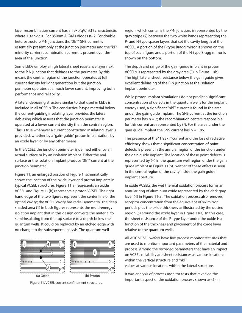
Figure 11, an enlarged portion of Figure 1, schematicallyshows the location of the oxide layer and proton implants intypical VCSEL structures. Figure 11(a) represents an oxideVCSEL and Figure 11(b) represents a proton VCSEL. The righthand edge of the two figures represent the center line of theoptical cavity; the VCSEL cavity has radial symmetry. The deepshaded area (1) in both figures represents the multi-energyisolation implant that in this design converts the material tosemi-insulating from the top surface to a depth below thequantum wells. It could be replaced by an etched edge withno change to the subsequent analysis. The quantum well
region, which contains the P-N junction, is represented by thegray stripe (2) between the two white bands representing theP- and N-type spacer layers that set the cavity length of theVCSEL. A portion of the P-type Bragg mirror is shown on thetop of each figure and a portion of the N-type Bragg mirror isshown on the bottom.
The depth and range of the gain-guide implant in protonVCSELs is represented by the gray area (3) in Figure 11(b). The high lateral sheet resistance below the gain guide givesexcellent debiasing of the P-N junction at the isolationimplant perimeter.
While proton implant simulations do not predict a significantconcentration of defects in the quantum wells for the implantenergy used, a significant “nkT” current is found in the areaunder the gain guide implant. The SNS current at the junctionperimeter has n = 2; the recombination centers responsiblefor this current are represented by (*). For the area under thegain guide implant the SNS current has n = 1.85.
The presence of the “1.85kT” current and the loss of radiativeefficiency shows that a significant concentration of pointdefects is present in the annular region of the junction underthe gain guide implant. The location of these point defects isrepresented by (+) in the quantum well region under the gainguide implant in Figure 11(b). Neither of these effects is seenin the central region of the cavity inside the gain guideimplant aperture.
In oxide VCSELs the wet thermal oxidation process forms anannular ring of aluminum oxide represented by the dark graylayer (4) in Figure 11(a). The oxidation process also removesacceptor concentration from the equivalent of six mirrorperiods plus the oxide thickness as illustrated by the dottedregion (5) around the oxide layer in Figure 11(a). In this case,the sheet resistance of the P-type layer under the oxide is afunction of the thickness and placement of the oxide layerrelative to the quantum wells.
All AOC VCSEL wafers have five process monitor test sites thatare used to monitor important parameters of the material andprocess. Among the recorded parameters that have an impacton VCSEL reliability are sheet resistances at various locationswithin the vertical structure and “nkT” values at various locations within the lateral structure.
It was analysis of process monitor tests that revealed theimportant aspect of the oxidation process shown as (5) in
Figure 11. VCSEL current confinement structures.
(a) Oxide (b) Proton
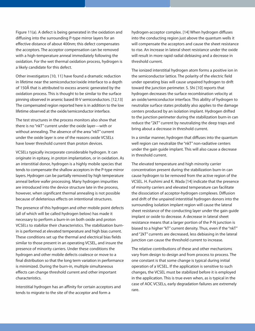
Figure 11(a). A defect is being generated in the oxidation anddiffusing into the surrounding P-type mirror layers for aneffective distance of about 400nm; this defect compensatesthe acceptors. The acceptor compensation can be removedwith a high-temperature anneal immediately following theoxidation. For the wet thermal oxidation process, hydrogen isa likely candidate for this defect.
Other investigators [10, 11] have found a dramatic reductionin lifetime near the semiconductor/oxide interface to a depthof 150Å that is attributed to excess arsenic generated by theoxidation process. This is thought to be similar to the surfacepinning observed in arsenic based III-V semiconductors. [12,13]The compensated region reported here is in addition to the lowlifetime observed at the oxide/semiconductor interface.
The test structures in the process monitors also show thatthere is no “nkT” current under the oxide layer—with orwithout annealing. The absence of the area “nkT” currentunder the oxide layer is one of the reasons oxide VCSELs have lower threshold current than proton devices.
VCSELs typically incorporate considerable hydrogen. It canoriginate in epitaxy, in proton implantation, or in oxidation. Asan interstitial donor, hydrogen is a highly mobile species thattends to compensate the shallow acceptors in the P-type mirrorlayers. Hydrogen can be partially removed by high temperatureanneal before wafer processing. Many hydrogen impuritiesare introduced into the device structure late in the process,however, when significant thermal annealing is not possiblebecause of deleterious effects on intentional structures.
The presence of this hydrogen and other mobile point defects(all of which will be called hydrogen below) has made itnecessary to perform a burn-in on both oxide and protonVCSELs to stabilize their characteristics. The stabilization burn-in is performed at elevated temperature and high bias current.These conditions set up the thermal and electrical bias fieldssimilar to those present in an operating VCSEL, and insure thepresence of minority carriers. Under these conditions thehydrogen and other mobile defects coalesce or move to afinal distribution so that the long term variation in performanceis minimized. During the burn-in, multiple simultaneouseffects can change threshold current and other importantcharacteristics.
Interstitial hydrogen has an affinity for certain acceptors andtends to migrate to the site of the acceptor and form a
hydrogen-acceptor complex. [14] When hydrogen diffusesinto the conducting region just above the quantum wells itwill compensate the acceptors and cause the sheet resistanceto rise. An increase in lateral sheet resistance under the oxidewill result in more rapid radial debiasing and a decrease inthreshold current.
The ionized interstitial hydrogen atom forms a positive ion inthe semiconductor lattice. The polarity of the electric fieldunder operating bias will cause unpaired hydrogen to drifttoward the junction perimeter. S. Shi [10] reports thathydrogen decreases the surface recombination velocity at an oxide/semiconductor interface. This ability of hydrogen toneutralize surface states probably also applies to the damagecenters produced by an isolation implant. Hydrogen drifted to the junction perimeter during the stabilization burn-in canreduce the “2kT” current by neutralizing the deep traps andbring about a decrease in threshold current.
In a similar manner, hydrogen that diffuses into the quantumwell region can neutralize the “nkT” non-radiative centersunder the gain guide implant. This will also cause a decreasein threshold current.
The elevated temperature and high minority carrierconcentration present during the stabilization burn-in cancause hydrogen to be removed from the active region of theVCSEL. H. Fushimi and K. Wada [14] indicate that the presenceof minority carriers and elevated temperature can facilitatethe dissociation of acceptor-hydrogen complexes. Diffusionand drift of the unpaired interstitial hydrogen donors into thesurrounding isolation implant region will cause the lateralsheet resistance of the conducting layer under the gain guideimplant or oxide to decrease. A decrease in lateral sheetresistance means that a larger portion of the P-N junction isbiased to a higher “kT” current density. Thus, even if the “nkT”and “2kT” currents are decreased, less debiasing in the lateraljunction can cause the threshold current to increase.
The relative contributions of these and other mechanismsvary from design to design and from process to process. Theone constant is that some change is typical during initialoperation of a VCSEL. If the application is sensitive to suchchanges, the VCSEL must be stabilized before it is employedin the application. This is true even when, as is typical in thecase of AOC VCSELs, early degradation failures are extremelyrare.
WAFER-LEVEL STABILIZATION AND STABILAZE
STABILAZE is the trademarked AOC VCSEL wafer-levelstabilization process. It conditions critical VCSEL deviceparameters at wafer level to be unvarying, duplicating theresults of and eliminating the requirement for subsequentpackage level burn-in, thereby improving cost efficiency andmaking wafer level selection of key parameter uniformity (forarray product applications) practical.
Figure 12 illustrates why stabilization is so important. Unlessthe VCSEL is subjected to a burn-in of some sort prior to ship-ment, it may take minutes, days, or weeks for the operatingcharacteristics to reach their final values. The magnitude ofthe changes depends on the specific VCSEL design and on the operating conditions. The devices in Figure 12 have anunusually high amount of variation during early operation;this was a result of a design tradeoff in which a particular finaloperating characteristic was optimized at the expense ofshort-term variation. It is always possible to do a stabilizationburn-in at a later assembly stage, but it is almost always lessdesirable to do so—only partly because it is more costly.
The STABILAZE process was developed and optimized toprovide equivalent or better results to package levelstabilization burn-in. Equipment, materials, and processtechniques were defined to contact, without damage, all diceacross the wafer for uniform bias current and uniform wafertemperature. A mechanically compressible, electrically andthermally conductive contact material was identified to
provide contact without mechanical damage. High thermaldissipation (>2000 watts/wafer) was a key equipment require-ment. Device design was refined to assure wafer level biascurrent flow duplicated package level operation. Extensivecharacterization and reliability testing on many (hundreds of ) wafers verified short term stabilization and long termreliability, using the wafer by wafer qualification processdescribed in reference [6] and accelerated burn-in testing at 100-150?C to compare failure rates with existing devicereliability models.
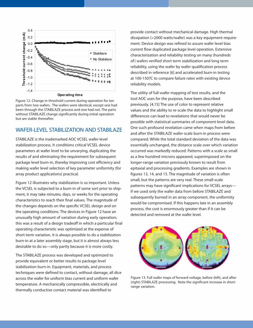
The utility of full-wafer mapping of test results, and the tool AOC uses for the purpose, have been describedpreviously. [4,15] The use of color to represent relative values and the ability to re-scale the data to highlight smalldifferences can lead to revelations that would never bepossible with statistical summaries of component-level data.One such profound revelation came when maps from beforeand after the STABILAZE wafer-scale burn-in process werecompared. While the total standard deviation of the data wasessentially unchanged, the distance scale over which variationoccurred was markedly reduced. Patterns with a scale as smallas a few hundred microns appeared, superimposed on thelonger-range variation previously known to result fromepitaxial and processing gradients. Examples are shown infigures 13, 14, and 15. The magnitude of variation is oftensmall, but the patterns are very real. These small-scalepatterns may have significant implications for VCSEL arrays—if we used only the wafer data from before STABILAZE andsubsequently burned in an array component, the uniformitywould be compromised. If this happens late in an assemblyprocess, the cost is enormously greater than if it can bedetected and removed at the wafer level.
-1.4
-1.2
-1.0
-0.8
-0.6
-0.4
-0.2
0.0
0.2
0.4
Operating time
Thre
shol
d cu
rren
t cha
nge
(mA
)
Stabilaze
No Stabilaze
Figure 12. Change in threshold current during operation for tenparts from two wafers. The wafers were identical, except one hadbeen through the STABILAZE process and one had not. The partswithout STABILAZE change significantly during initial operation but are stable thereafter.
Figure 13. Full wafer maps of forward voltage, before (left), and after(right) STABILAZE processing. Note the significant increase in short-range variation.
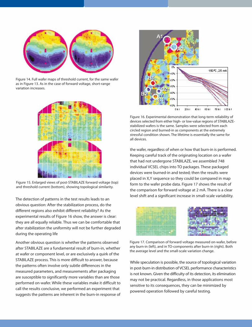
The detection of patterns in the test results leads to anobvious question: After the stabilization process, do thedifferent regions also exhibit different reliability? As theexperimental results of Figure 16 show, the answer is clear:they are all equally reliable. Thus we can be comfortable thatafter stabilization the uniformity will not be further degradedduring the operating life
Another obvious question is whether the patterns observedafter STABILAZE are a fundamental result of burn-in, whetherat wafer or component level, or are exclusively a quirk of theSTABILAZE process. This is more difficult to answer, becausethe patterns often involve only subtle differences in themeasured parameters, and measurements after packaging are susceptible to significantly more variables than are thoseperformed on-wafer. While these variables make it difficult tocall the results conclusive, we performed an experiment thatsuggests the patterns are inherent in the burn-in response of
the wafer, regardless of when or how that burn-in is performed.Keeping careful track of the originating location on a waferthat had not undergone STABILAZE, we assembled 748individual VCSEL chips into TO packages. These packageddevices were burned-in and tested; then the results wereplaced in X,Y sequence so they could be compared in mapform to the wafer probe data. Figure 17 shows the result ofthe comparison for forward voltage at 2 mA. There is a clearlevel shift and a significant increase in small-scale variability.
While speculation is possible, the source of topological variationin post-burn-in distribution of VCSEL performance characteristicsis not known. Given the difficulty of its detection, its eliminationmay not be practical. Regardless, in those applications mostsensitive to its consequences, they can be minimized bypowered operation followed by careful testing.
Figure 14. Full wafer maps of threshold current, for the same waferas in Figure 13. As in the case of forward voltage, short-rangevariation increases.
Figure 15. Enlarged views of post-STABILAZE forward voltage (top)and threshold current (bottom), showing topological similarity.
Figure 16. Experimental demonstration that long-term reliability ofdevices selected from either high- or low-value regions of STABILAZE-stabilized wafers is the same. Samples were selected from eachcircled region and burned-in as components at the extremelystressful condition shown. The lifetime is essentially the same for all devices.
Figure 17. Comparison of forward voltage measured on-wafer, beforeany burn-in (left), and in TO-components after burn-in (right). Boththe average level and the small-scale variation change.
CONCLUSIONS
AOC’s extensive reliability work for its proton VCSEL has beenextended to several varieties of its oxide VCSEL. All this testingpays off—the parametric and reliability effects of the designspace are now well understood. Reliability testing for large (17?m), medium (14 ?m), and small (5 ?m) diameter oxideapertures shows that the larger device generally gives betterreliability for expected application currents. However,different conclusions may be reached depending on theparameter of greatest importance. So reliability is in the eyeof the beholder, who should also understand the assumptionsunderlying reported reliability models, as they can dramaticallyaffect the conclusions reached. Neither infant mortality norrandom failure appear to be a significant issue in our well-controlled tests; however, smaller aperture VCSELs have muchlower thresholds to ESD which may lead to random failuresdue to improper handling. Humidity resistance is excellent forall sizes of AOC’s oxide VCSEL. Finally, a key component ofVCSEL reliability is ensuring parameters remain stable overtime (distinct from degradation). While in the past this hastypically been achieved through component-level burn-in,AOC has now developed the STABILAZE process, whichstabilizes the VCSEL parametric performance while still inwafer form.
So through painstaking study of both short-term variationand long-term reliability, AOC has been able to develop theappropriate design boundaries and process windows toachieve stable, reliable oxide VCSELs of several types to servethe various user needs. This is only possible by combiningstatistical experimentation techniques like design-of-experiments with production-scale analysis tools such aswafer maps to study a wide range of designs. It is crucial toexplore the design possibilities, not just the design that willbe the final product, before these islands of reliability can befully defined.
ACKNOWLEDGMENTS
The authors wish to acknowledge the contributions of MikeHaji-Sheikh, MiCha Hatfield, Simon Rabinovich, and FredWinn.
REFERENCES
1. Guenter, J., et al., “Commercialization of AOC’s VCSELTechnology: Further Developments,” in Vertical-CavitySurface-Emitting Lasers V, Choquette, K.D. and Lei, C.,editors, Proceedings of the SPIE Vol. 4286, (2001), pp. 1-14.
2. Herrick, R.W., et al., “Highly reliable oxide VCSELsmanufactured at HP/Agilent Technologies,” in Vertical-Cavity Surface-Emitting Lasers IV, Choquette, K.D. andLei, C., editors, Proceedings of the SPIE Vol. 3946, (2000),pp. 14-19.
3. Wipiejiewski, T., et al., “VCSELs for datacom applications,”,” in Vertical-Cavity Surface-Emitting Lasers III, Choquette,K.D. and Lei, C., editors, Proceedings of the SPIE Vol. 3627,(1999), pp. 14-22.
4. Tatum, Jim A., et al., “Commercialization of AOC’s VCSELTechnology,” in Vertical-Cavity Surface-Emitting Lasers IV,Choquette, K.D. and Lei, C., editors, Proceedings of theSPIE Vol. 3946, (2000), pp. 2-13.
5. Guenter, J., et al., “Reliability of proton-implanted VCSELsfor data communications,” in Fabrication, Testing, andReliability of Semiconductor Lasers, Fallahi, M. and Wang,S. editors, Proceedings of the SPIE, vol. 2683, (1996), pp.102-113.
6. Hawthorne, R.A, et al., “Reliability Study of 850 nmVCSELs for Data Communications,” 1996 IEEEInternational Reliability Physics Proceedings, 34, (1996),pp. 203-210.
7. Maeda, K., and Takeuchi, S., “Enhanced Glide ofDislocations in GaAs Single Crystals by Electron BeamIrradiation,” Japanese Journal of Applied Physics, vol. 20,no. 3 (1981), pp. L165-L168.
8. Peck, D. Stewart, “Comprehensive Model for HumidityTesting Correlation,” 1986 IEEE International ReliabilityPhysics Proceedings; (1986), pp. 44-50.
9. Sah, C-T, et al., “Carrier Generation and Recombination inP-N Junctions and P-N Junction Characteristics,”Proceedings of the IRE, September 1957, pp 1228-1243.
10. Shi, S., et al., “Photoluminescence study of hydrogenatedaluminum oxide-semiconductor interface,” Appl. Phys.Lett. 70 (10), 10 March 1997; pp 1293-1295.
11. Kash, J.A., et al., “Recombination in GaAs at the AlAsoxide-GaAs interface,” Appl. Phys. Lett. 67 (14), 2 October1995; pp 2022-2024.
12. H. H. Wieder, “Fermi level and surface barrier of GaxIn1-xAs alloys,” Appl. Phys. Lett. 38 (3), 1 February 1981; pp170-171.
13. Spicer, W.E., et al., “The Unified Model For Schottky BarrierFormation and MOS Interface States in 3-5 Compounds,”Applications of Surface Science, 9 (1981); pp 83-91.
14. Fushimi, H., and Wada, K, “Degradation Mechanism inCarbon-doped GaAs Minority-carrier Injection Devices,”1966 IEEE International Reliability Physics Proceedings;(1996), pp. 214-220.
15. Farrier, R.C. “Parametric control for wafer fabrication: newCIM techniques for data analysis,” Solid State Technology,September 1997.
16. Herrick, R.W., “Oxide VCSEL qualification at AgilentTechnologies,” in Vertical-Cavity Surface-Emitting LasersVI, Lei, C. and Kilcoyne, S. editors, Proceedings of theSPIE, vol. 4649, (2002), in press.
17. Lowes, T.D., “VCSEL reliability research at Gore Photonics,”in Vertical-Cavity Surface-Emitting Lasers VI, Lei, C. andKilcoyne, S. editors, Proceedings of the SPIE, vol. 4649,(2002), in press.
18. Osenbach, J.W., and Evanosky, T.L., “Temperature-Humidity-Bias Behavior and Acceleration Model for InPPlanar PIN Photodiodes,” Journal of LightwaveTechnology, vol. 14, no. 8, (1996), pp. 1865-1881
©2007 Finisar Corporation. All rights reserved. Finisar is a registered trademark of Finisar Corporation. Features and specifications are subject to change without notice. 1/07
Phone:1-866-MY-VCSEL USA (toll free) 1-972-792-1800 USA (Direct dial) 44 (0) 174 336 5533 Europe 886-935-409898 China & Taiwan81-90-4437-1130 Japan82-11-220-6153 Asia Pacific & Korea
ADVANCED OPTICAL COMPONENTSFinisar’s ADVANCED OPTICAL COMPONENTS division wasformed through strategic acquisition of key optical compon-ent suppliers. The company has led the industry in highvolume Vertical Cavity Surface Emitting Laser (VCSEL) andassociated detector technology since 1996. VCSELs havebecome the primary laser source for optical data communi-cation, and are rapidly expanding into a wide variety of sensorapplications. VCSELs’ superior reliability, low drive current,high coupled power, narrow and circularly symmetric beamand versatile packaging options (including arrays) are enablingsolutions not possible with other optical technologies.ADVANCED OPTICAL COMPONENTS is also a key supplier ofFabrey-Perot (FP) and Distributed Feedback (DFB) Lasers, andOptical Isolators (OI) for use in single mode fiber data andtelecommunications networks
LOCATIONAllen, TX - Business unit headquarters, VCSEL wafergrowth, wafer fabrication and TO package assembly.
Fremont, CA – Wafer growth and fabrication of 1310 to1550nm FP and DFB lasers.
Shanghai, PRC – Optical passives assembly, includingoptical isolators and splitters.
SALES AND SERVICEFinisar’s ADVANCED OPTICAL COMPONENTS division serves itscustomers through a worldwide network of sales offices anddistributors. For application assistance, current specifications,pricing or name of the nearest Authorized Distributor, contacta nearby sales office or call the number listed below.
AOC CAPABILITIESADVANCED OPTICAL COMPONENTS’ advanced capabilitiesinclude:
1, 2, 4, 8, and 10Gbps serial VCSEL solutions
1, 2, 4, 8, and 10Gbps serial SW DETECTOR solutions
VCSEL and detector arrays
1, 2, 4, 8, and 10Gbps FP and DFB solutions at 1310 and1550nm
1, 2, 4, 8, and 10Gbps serial LW DETECTOR solutions
Optical Isolators from 1260 to 1600nm range
Laser packaging in TO46, TO56, and Opticalsubassemblies with SC, LC, and MU interfaces forcommunication networks
VCSELs operating at 670nm, 780nm, 980nm, and 1310nmin development
Sensor packages include surface mount, various plastics,chip on board, chipscale packages, etc.
Custom packaging options
Fax: 1-214-509-3709 USA
Email: [email protected]: www.finisar.com/aoc.php


![APPLICATION Plasma Processes BRIEF for VCSELs · 2018-07-26 · Geography - Global Forecast to 2022” MarketsandMarkets [3] “Vertical Cavity Surface Emitting Laser (VCSELs) Market](https://static.fdocuments.us/doc/165x107/5ed97bd11b54311e7967a587/application-plasma-processes-brief-for-vcsels-2018-07-26-geography-global-forecast.jpg)


![APPLICATION Plasma Processes BRIEF for VCSELs · Geography - Global Forecast to 2022” MarketsandMarkets [3] “Vertical Cavity Surface Emitting Laser (VCSELs) Market - Global Industry](https://static.fdocuments.us/doc/165x107/5f9d30cf2e8f9d72ea258e2c/application-plasma-processes-brief-for-vcsels-geography-global-forecast-to-2022a.jpg)