QUALIi1 X ?ilOiJijD ' Reproduced From Best Available Copy
36
AFRL-ML-WP-TR-1998-4184 INGAP/GAAS QUANTUM WELL INFRARED PHOTODETECTORS N. PAN J. FAN KOPIN CORPORATION 695 MYLES STANDISH BOULEVARD TAUNTON, MA 02780 AUGUST 1997 FINAL REPORT FOR 09/01/1993 - 02/01/1997 THIS IS A SMALL BUSINESS INNOVATION RESEARCH (SBIR) PHASE II REPORT APPROVED FOR PUBLIC RELEASE; DISTRIBUTION IS UNLIMITED, MATERIALS AND MANUFACTURING DIRECTORATE AIR FORCE RESEARCH LABORATORY AIR FORCE MATERIEL COMMAND WRIGHT PATTERSON AFB OH 45433-7734 Reproduced From Best Available Copy QUALIi 1 X * - ?ilO"i"JijD '
Transcript of QUALIi1 X ?ilOiJijD ' Reproduced From Best Available Copy

AFRL-ML-WP-TR-1998-4184
INGAP/GAAS QUANTUM WELL INFRARED PHOTODETECTORS
N. PAN J. FAN
KOPIN CORPORATION 695 MYLES STANDISH BOULEVARD TAUNTON, MA 02780
AUGUST 1997
FINAL REPORT FOR 09/01/1993 - 02/01/1997
THIS IS A SMALL BUSINESS INNOVATION RESEARCH (SBIR) PHASE II REPORT
APPROVED FOR PUBLIC RELEASE; DISTRIBUTION IS UNLIMITED,
MATERIALS AND MANUFACTURING DIRECTORATE AIR FORCE RESEARCH LABORATORY AIR FORCE MATERIEL COMMAND WRIGHT PATTERSON AFB OH 45433-7734
Reproduced From Best Available Copy
QUALIi1 X *■■- ?ilO"i"JijD '

NOTICE
USING GOVERNMENT DRAWINGS, SPECIFICATIONS, OR OTHER DATA INCLUDED IN THIS DOCUMENT FOR ANY PURPOSE OTHER THAN GOVERNMENT PROCUREMENT DOES NOT IN ANY WAY OBLIGATE THE US GOVERNMENT. THE FACT THAT THE GOVERNMENT FORMULATED OR SUPPLIED THE DRAWINGS, SPECIFICATIONS, OR OTHER DATA DOES NOT LICENSE THE HOLDER OR ANY OTHER PERSON OR CORPORATIONOR CONVEY ANY RIGHTS OR PERMISSION TO MANUFACTURE, USE, OR SELL ANY PATENTED INVENTION THAT MAY RELATE TO THEM.
THIS REPORT IS RELEASABLE TO THE NATIONAL TECHNICAL INFORMATION SERVICE (NTIS). AT NTIS, IT WILL BE AVAILABLE TO THE GENERAL PUBLIC, INCLUDING FOREIGN NATIONS.
THIS TECHNICAL REPORT HAS BEEN REVIEWED AND IS APPROVED FOR PUBLICATION.
tj(H2^^ GAEL y. BROWN, Project Engineer Sensor Materials Branch Survivability & Sensor Materials Division
I & ROBERT L. DENISON, Chief Sensor Materials Branch Survivability & Sensor Materials Division
WILLIAM R. WOODY, Cltfef Survivability & Sensor Materials Division Materials & Manufacturing Directorate
Do not return copies of this report unless contractual obligations or notice on a specific document require its return.

REPORT DOCUMENTATION PAGE Form Approved
OMB No. 0704-0188
jD1:: resr-'tmc buraen Tor tms collection of information is estimated to average 1 nour oer response. mc!'jd<-.g tre time -c reviewing instructions. se — -v-z exiting aata sources, ! aatnerma and rnamtaimna the data needed, and completing and reviewing the collection of information. Sena comments regarding this burden estimate or an, ctner aspect of this
~ i;e:t.n^ o' information,"including suggestions for reducing this Durden, to Wasninaton Headauarters Services, Directorate for Information Operations and Peoorts, 1215 Jefferson Oa.-s Hi^nAay, Suite 12CX, Arlington. VA 22202-4302. and to the Office of Management and Budget, Paperwork Pedu-tion Pro*ect (0704-0188), Washington, TC 20503
1. AGEK'CY USE ONLY (Leave blank) 2. REPORT DATF
ftUff 1997
3. REPORT TVE AMD DATES COVERED
.EINM» £LSLZ 4. TITLE AND SUBTITLE INGAP/GAAS QUANTUM WELL INFRARED
PHOTODETECTORS
6. AUTKOR(S)N_ pAN
J. FAN
7. PERFORMING ORGANIZATION NAME(S) AND ADDRESS(ES)
KOPIN CORPORATION 695 MYLES STANDISH BOULEVARD TAUNTON. MA 02780
m /iQQ3~n9/m /IQQ7 5. FUNDING NUMBERS
C F33615-93-C-5382 PE 35885 PR 3005 TA 0 5 WU 84
PERFORMING ORGANIZATION REPORT NUMBER
9. SPONSORING/MONITORING AGENCY NAME(S) AND ADDRESS(ES)
MATERIALS AND MANUFACTURING DIRECTORATE AIR FORCE RESEARCH LABORATORY AIR FORCE MATERIEL COMMAND WRIGHT PATTERSON AFB OH 45433-7734
POC: Gail j. Brown, AFRL/MLPO, 937-255-4474 ext. 3238
10. SPONSORING/MONITORING AGENCY REPORT NUMBER
AFRL-ML-WP-TR-1998-4184
11. SUPPLEMENTARY NOTES PUBLIC RELEASE CLEARANCE ASC-97-1497, 15 JUL 98
12a. DISTRIBUTION/AVAILABILITY STATEMENT
APPROVED FOR PUBLIC RELEASE; DISTRIBUTION IS UNLIMITED.
| 12b. DISTRIBUTION CODE
19981230 081 13. ACSTRACT (Maximum 200 words) THIS IS A SBIR PHASE II REPORT
THE OBJECTIVE OF THIS PHASE II SBIR WAS TO IMPROVE THE QUALITY OF MULTI-QUANTUM WELL MATERIALS SUITABLE FOR INFRARED DETECTOR APPLICATIONS AND TO INVESTIGATE NOVEL BANDGAP ENGINEERING CONCEPTS UTILIZING InGaP/GaAs HETEROSTRUCTURE MATERIALS. THE SUBCONTRACTOR, NORTHWESTERN UNIVERSITY, WAS SUCCESSFUL IN GROWING HIGH QUALITY InGaP/GaAs MULTIQUANTUM WELL MATERIALS BY LOW PRESSURE METAL-ORGANIC CHEMICAL VAPOR DEPOSITION (MOCVD), AND IN DEMONSTRATING IMPROVED PERFORMANCE IN THE PHOTODETECTOR TEST STRUCTURES FABRICATED FROM THESE MATERIALS. MOST OF THE RESULTS IN THIS REPORT ARE FROM THE RESEARCH WORK AT NORTHWESTERN UNIVIERSITY. THE PRIME CONTRACTOR, KOPIN CORPORATION, WAS NOT SUCCESSFUL IN TRANSFERING THE GROWTH PARAMETERS FOR THESE MATERIALS FROM NORTHWESTERN UNIVERSITY TO THEIR PRODUCTION-SCALE MOCVD REACTORS. NO REPORTABLE RESULTS WERE OBTAINED ON THE KOPIN MATERIALS.
U. SUBJECT TERMS
SBIR PHASE II REPORT PHOTODETECTORS, INFRARED, QUANTUM WELLS, INGAP,
„MÜCiüL
15. NUMBER OF PAGES
16. PiuCE CODE -—35-
ü
17. SECURITY CLASSIFICATION OF REPORT
UNCLASSIFIED
18. SECURITY CLASSIFICATION OF THIS PAGE UNCLASSIFIED
19. SECURITY CLASSIFICATION OF ABSTRACT UNCLASSIFIED
20. LIViTATiON OF ABSTRACT]
SAR j
NSN 7540-01-280-5500 Standard -orm, 2JS (Rev. 2-89} Pres.-ibcs P. ANS: S-rj :59-18

Final Report
EXECUTIVE SUMMARY
Most of the quantum well intersubband photodetector (QWIP) research has
focused on multiple quantum well heterostructures of GaAs and AlxGa,.xAs due to
the epitaxial growth and processing maturity of these materials. However, the
magnitude of the dark currents in GaAs/AlGaAs QWIPs remained large for
optimum connection to readout electronics, especially as the devices are extended
to longer wavelength operational] One way to improve the performance of these
QWIPs is to replace the AlGaAs barrier with lattice-matched GalnP or GalnAsP
alloys. The GaxIn,.xAsyP,.y system has been investigated for the growth of lattice
matched heterostructures of GalnAsP/GaAs (1-v =2.13*) and GalnAsP/InP
(y * 2.2JC). Reviews of these systems have been published [2,3]. The quaternary
composition range for lattice matched GalnAsP/InP includes the two optical fiber
communication windows known today: zero dispersion at X = 1.3 |im and
minimum loss at X = 1.55 UMn [4,5]. Today, GalnAsP/InP lasers are the mainstay
of optical communication systems.
The InGaAsP/GaAs material system did not develop as rapidly because it covered
the same wavelength range as the A^Ga^As/GaAs material system, which was
more widely developed. The AlGaAs/GaAs system was attractive because of its
perfect lattice match to GaAs for all Al compositions. However, the lifetime of
laser systems based on AlGaAs/GaAs laser diodes is limited by the laser diode
lifetime due to problems connected with the presence of Al in the diode materials.
High interaction of Al with oxygen leads to oxide formation at the mirror facet
and enhances the non-radiative recombination of injected carriers near the mirror
facet which creates the overheating of the mirror, and decreases the lifetime.
Another lifetime limiting factor for AlGaAs-based laser diodes is the formation
of dark-line defects, as a consequence of the spreading of the dislocations in the
Final Report
active region during high-power operation. These problems have been solved by
the replacement of AlGaAs with the Al-free GalnAsP/GaAs system. [6,7].
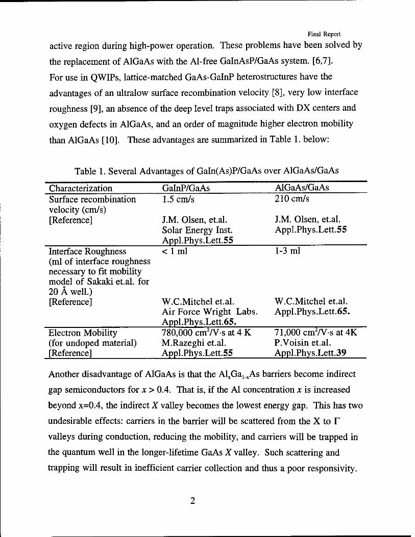
For use in QWIPs, lattice-matched GaAs-GalnP heterostructures have the
advantages of an ultralow surface recombination velocity [8], very low interface
roughness [9], an absence of the deep level traps associated with DX centers and
oxygen defects in AlGaAs, and an order of magnitude higher electron mobility
than AlGaAs [10]. These advantages are summarized in Table 1. below:
Table 1. Several Advantages of GaIn(As)P/GaAs over AlGaAs/GaAs
Characterization GalnP/GaAs AlGaAs/GaAs Surface recombination velocity (cm/s) [Reference]
1.5 cm/s
J.M. Olsen, et.al. Solar Energy Inst. Appl.Phys.Lett.55
210 cm/s
J.M. Olsen, et.al. Appl.Phys.Lett.55
Interface Roughness (ml of interface roughness necessary to fit mobility model of Sakaki et.al. for 20 A well.) [Reference]
< 1ml 1-3 ml
W.C.Mitchel et.al. Air Force Wright Labs. Appl.Phys.Lett.65.
W.C.Mitchel et.al. Appl.Phys.Lett.65.
Electron Mobility (for undoped material) [Reference]
780,000 cm7V-s at 4 K M.Razeghi et.al. Appl.Phys.Lett.55
71,000 cm2/V-s at 4K P.Voisin et.al. Appl.Phys.Lett.39
Another disadvantage of AlGaAs is that the ALGa^As barriers become indirect
gap semiconductors for x > 0.4. That is, if the Al concentration x is increased
beyond x=0.4, the indirect X valley becomes the lowest energy gap. This has two
undesirable effects: carriers in the barrier will be scattered from the X to T
valleys during conduction, reducing the mobility, and carriers will be trapped in
the quantum well in the longer-lifetime GaAs X valley. Such scattering and
trapping will result in inefficient carrier collection and thus a poor responsivity.
Final Report
Although such indirect barrier QWIPs have been fabricated[ll], optimized
direct-bandgap AlGaAs/GaAs QWIPs are limited to cutoff wavelengths of 5.6(im.
Such a limitation does not exist in GalnAsP/GaAs. In a recent series of papers,
the merits of valence band GalnAsP based QWIPs have been introduced. [12-15]
The p-type (valence band) versions of these devices have shown photoresponse
from 2 out to 7 microns at normal incidence and have demonstrated background
limited photodetection up to sample temperatures of 120K.
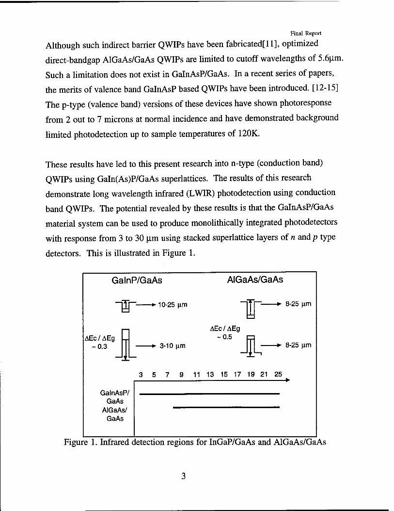
These results have led to this present research into n-type (conduction band)
QWIPs using GaIn(As)P/GaAs superlattices. The results of this research
demonstrate long wavelength infrared (LWIR) photodetection using conduction
band QWIPs. The potential revealed by these results is that the GalnAsP/GaAs
material system can be used to produce monolithically integrated photodetectors
with response from 3 to 30 Jim using stacked superlattice layers of n and/7 type
detectors. This is illustrated in Figure 1.
GalnP/GaAs AlGaAs/GaAs
~~pn— ► 10-25 |im
AEc/AEg -0.3
AEc/AEg -0.5
■*• 3-10 urn
T 4-
8-25 urn
8-25 |im
3 5 7 9 11 13 15 17 19 21 25
GalnAsP/ GaAs
AIGaAs/ GaAs
Figure 1. Infrared detection regions for InGaP/GaAs and AlGaAs/GaAs

Final Report
QUANTUM WELL CHARACTERIZATION
Wafer characterization will be divided into electrical, optical and structural
characterization techniques. For GaIn(As)P/GaAs based devices, the primary
focus of the characterization is the experimental determination of the device
parameters, i.e. the layer thicknesses and material compositions. Three
instruments are used for structural characterization: the analytical x-ray
diffractometer, the scanning electron microscope, and the transmission electron
microscope (TEM). Cross-sectional transmission electron microscopy was used
to measure the thicknesses of several GalnP/GaAs superlattices (100 A GaAs/523
Ä InGaP). A cross-section image of a 10 period superlattice is shown in Figure
2. Qualitatively the layers are very smooth without any apparent dislocations or
interface layers.
Figure 2. TEM photograph of a 10 period GalnP/GaAs superlattice.

Final Report
Quantitative measurements of the thickness of the wells and barriers are possible
by physically measuring the thicknesses on the photograph with a micrometer. o
Measurements for this sample yielded an average well thickness of 134 A o o
(standard deviation a = 7 A) and an average barrier thickness of 523 A (a = 8
Ä). The variation in thickness was likely due to measurement error.
Advanced x-ray diffraction measurements and simulation of superlattices are used
to "measure" the thicknesses of superlattice layers. X-ray diffraction spectra also
measure the lattice mismatch between the substrate and epilayer(s) and give a
quantitative measure of the film quality. A crystalline solid, consisting of a
regular array of atoms, can be regarded as a natural three-dimensional
diffraction grating for x-rays. Diffraction is governed by the Bragg equation:
2sin0s _ 1
I 1 where 0B is complementary to the angle of incidence, and d is the spacing
between two consecutive planes in the lattice. The wavelength of x-rays is of the
order of 10 "8 cm, whereas the smallest lattice periods lies in the range 10"8 ~ 10"5
cm. Accordingly, the scattering angles are large enough to be measured. For a
typical rocking curve measurement, the sample to be characterized is rotated
about the Bragg angle 0B, while the diffracted beam is measured. A typical x-ray
diffraction measurement for a lujm thick layer of GalnP grown on GaAs is
shown in figure 3.

Final Report
100000 F
10000
1000
100
10
GaAs GalnP mismatch-1500 ppm 1 um
jUiilinLJ^HlillL. 32.0 32.5 33.0 33.5 34.0
Omega(e)
Figure 3. X-ray diffraction spectrum for GalnP/GaAs.
For materials like GaJn^P, the peak separation between the epilayer and the
GaAs substrate can be used to determine the composition. The uniformity of the
X-ray splitting performed on a 4 inch InGaP is shown in Figure 4. The energy
gap is shown on the side of the figure. The uniformity across the wafer was
very good. The variation in energy gap across the wafer was 1.875 ±0.003 eV.
More advanced dynamic x-ray scattering theory must be used to evaluate the x-
ray diffraction spectra for superlattice samples. In multi-layer structures,
interference fringes in the diffraction spectrum occur due to interaction between
incident and reflected waves through different crystal layers, i.e. oscillations
occur when two waves diffracted from different structures interfere with each
other. The relation between the angular spacing of the fringes 0q and the

u in u
o o o o o m o m o m o CO co eg CM T— o o o o o o 1 lO o m o m o o 1
CO CN CM T— T— m o ■ E3 D D D D H
o
LL
u> c £
Q_ a (0 CO O > c m m■■ u
1 X
«5 1^ u. a> o 55'
D) (0 a.
a. o o CO
>
m oo h- oo
> > a> <D 00 05 CM CO r^ 1^- 00 00
Final Report
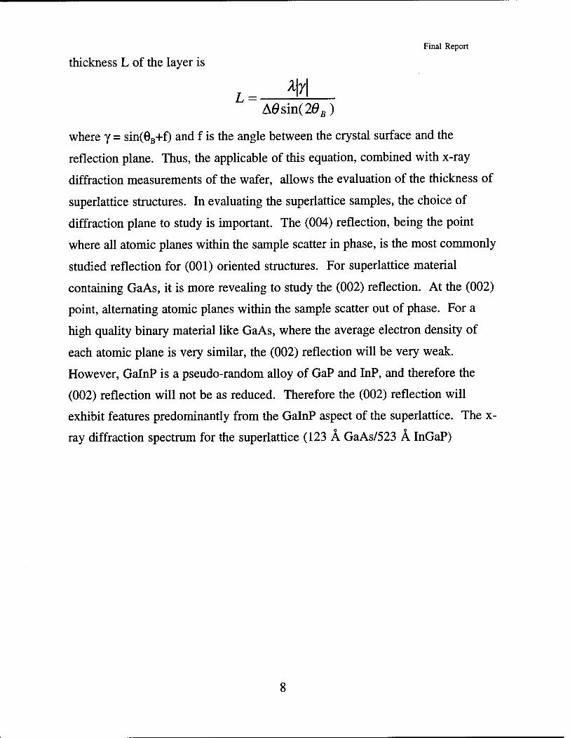
thickness L of the layer is
L= m A0sin(20s)
where y = sin(0B+f) and f is the angle between the crystal surface and the
reflection plane. Thus, the applicable of this equation, combined with x-ray
diffraction measurements of the wafer, allows the evaluation of the thickness of
superlattice structures. In evaluating the superlattice samples, the choice of
diffraction plane to study is important. The (004) reflection, being the point
where all atomic planes within the sample scatter in phase, is the most commonly
studied reflection for (001) oriented structures. For superlattice material
containing GaAs, it is more revealing to study the (002) reflection. At the (002)
point, alternating atomic planes within the sample scatter out of phase. For a
high quality binary material like GaAs, where the average electron density of
each atomic plane is very similar, the (002) reflection will be very weak.
However, GalnP is a pseudo-random alloy of GaP and InP, and therefore the
(002) reflection will not be as reduced. Therefore the (002) reflection will
exhibit features predominantly from the GalnP aspect of the superlattice. The x- o o
ray diffraction spectrum for the superlattice (123 A GaAs/523 A InGaP)
8

Final Report
observed by TEM is shown in Figure 5.
13 14 15 16 17 18
Omega / 2The» (degrees)
19 20
Figure 5 X-ray diffraction spectrum of 10 period (123 A GaAs/523 A InGaP)
superlattice.
Analysis of the spacing between interference fringes in this spectrum yield
average thicknesses of 123 Ä for the GaAs wells and 523Ä for the GalnP
barriers. Comparison with the TEM measurement suggests the accuracy of o
thickness measurement by x-ray diffraction simulation to be ~ 10A. Layer
thicknesses measured for QWIPs fabricated and tested as part of this research
were measured by x-ray diffraction, and have a similar accuracy. X ray
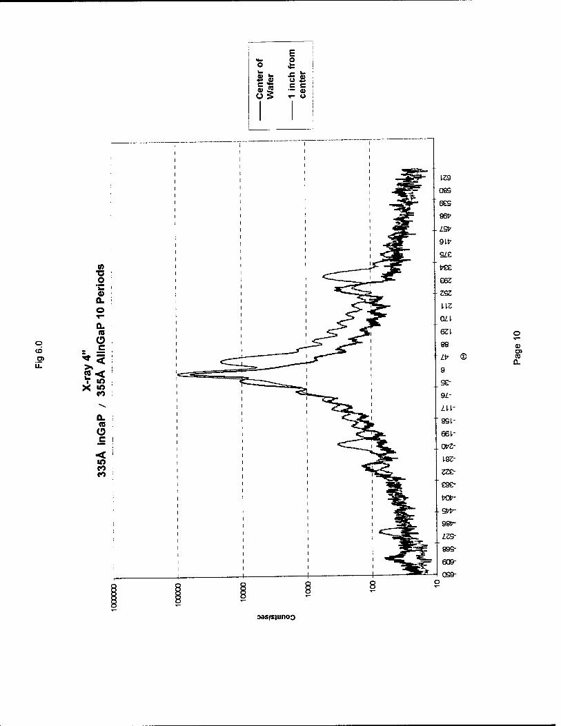
diffraction for a 4 inch 335 Ä InGaP/355 Ä AlGalnP 10 period structure
at two different positions across the wafer is shown in Figure 6. The spacing
between the fringes were very close indicating excellent control of the thickness.
E
1) u -Cm ~ ,£ o * = "= c c - 0) «- o Ü §
o CD
CD Ol CD Q.
Dasfsjunoo

Final Report
The slight shift in the peak position was due to the small shift in composition of
the layers.
Wafers grown with the complete QWIP structure contain many more superlattice
periods. The well thickness is also smaller than the above structure, resulting in a
smaller angular spacing between fringes. The measured diffraction spectrum and
a simulation for a 75 Ä GaAs/500 A InGaP QWIP is shown in figure 7.
20 Period Superlattice Period A = 575 Ä Well width = 75 A
Barrier = 500 Ä mismatch = 0.034%
Measured
Intensity (
Simulated
14 15
14 15 16
Omega (0)
17 18
Figure 7. X-ray diffraction spectrum of QWIP structure.
Typically, scanning electron microscopy was used to view the topography of a
surface, perhaps before and then after processing. However, the contrast in
11
Final Report
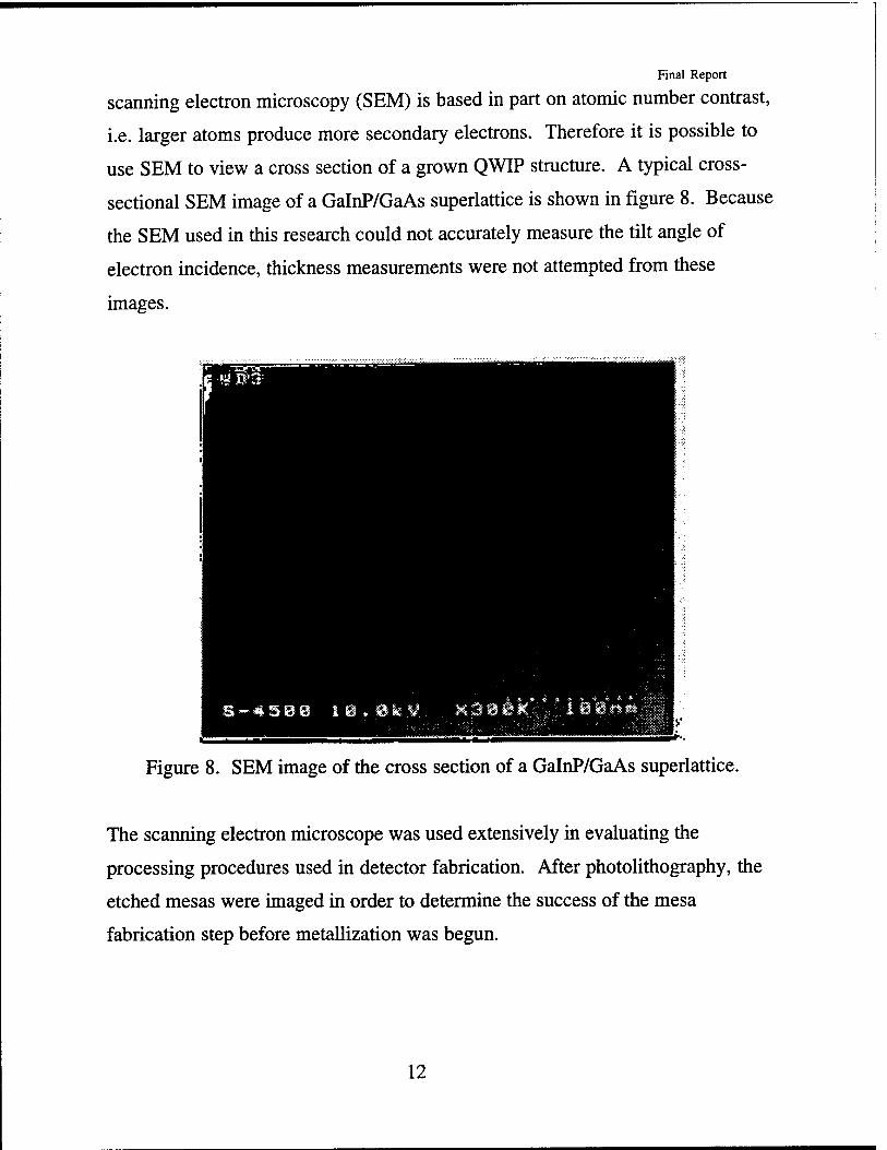
scanning electron microscopy (SEM) is based in part on atomic number contrast,
i.e. larger atoms produce more secondary electrons. Therefore it is possible to
use SEM to view a cross section of a grown QWIP structure. A typical cross-
sectional SEM image of a GalnP/GaAs superlattice is shown in figure 8. Because
the SEM used in this research could not accurately measure the tilt angle of
electron incidence, thickness measurements were not attempted from these
images.
Figure 8. SEM image of the cross section of a GalnP/GaAs superlattice.
The scanning electron microscope was used extensively in evaluating the
processing procedures used in detector fabrication. After photolithography, the
etched mesas were imaged in order to determine the success of the mesa
fabrication step before metallization was begun.
12

Final Report
Photoluminescence (PL) is one of the most useful characterization methods for
the semiconductor industry. Its most common use is the determination of
bandgap for ternary and quaternary alloys, such as GaJn^P. Since the relation
between the bandgap and composition JC is known, a measurement of the bandgap
can be inverted to determine x. PL is also sensitive to impurities, and PL
spectrum peaks can be used to identify the type of impurity. In another use, the
halfwidths of PL peaks are an indication of sample quality and crystallinity. PL
spectrum presented in this proposal were measured using the 514 nm line of an
Argon (Ar+) ion laser, at sample temperatures from 77 - 300K, and excitation
intensities of approximately 1 W cm"2. Samples of GaxIn1.xAsyP1.y were grown
with varying compositions x and y such that they covered the entire range of
compositions from GaAs to GalnP. The result is shown in Figure 9.
1.0 -
0.8
0.6 -
0.4 -
0.2 -
0.0 -
1.84 eV GalnAsP
1.43 eV A 1.55ev A 1.77eV f 1.9eV
GaAs / ' GalnAsPj I GalnAsrf GalnP
1.4 1.6 1.8
Bandgap Energy (eV)
20
Figure 9. 300 K Photoluminescence of GaJn^As Pj for varying compositions
13
Final Report
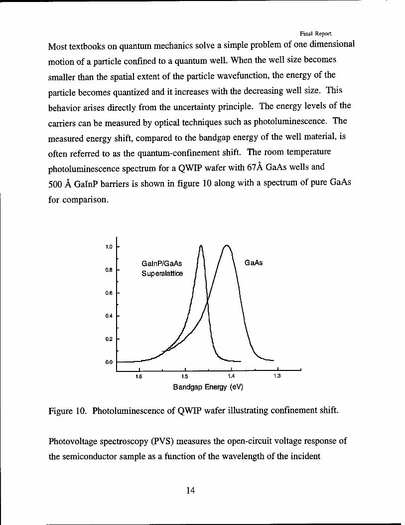
Most textbooks on quantum mechanics solve a simple problem of one dimensional
motion of a particle confined to a quantum well. When the well size becomes
smaller than the spatial extent of the particle wavefunction, the energy of the
particle becomes quantized and it increases with the decreasing well size. This
behavior arises directly from the uncertainty principle. The energy levels of the
carriers can be measured by optical techniques such as photoluminescence. The
measured energy shift, compared to the bandgap energy of the well material, is
often referred to as the quantum-confinement shift. The room temperature
photoluminescence spectrum for a QWIP wafer with 67Ä GaAs wells and
500 Ä GalnP barriers is shown in figure 10 along with a spectrum of pure GaAs
for comparison.
1.0
0.8 GalnP/GaAs I I Superalattice J I
/ \ GaAs
0.6 / l/
0.4
0.2
0.0 i ■ i »— i . i...
1.6 1.5 1.4 1.3
Bandgap Energy (eV)
Figure 10. Photoluminescence of QWIP wafer illustrating confinement shift.
Photovoltage spectroscopy (PVS) measures the open-circuit voltage response of
the semiconductor sample as a function of the wavelength of the incident
14
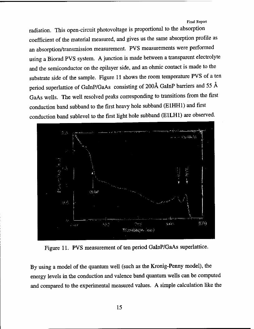
Final Report
radiation. This open-circuit photovoltage is proportional to the absorption
coefficient of the material measured, and gives us the same absorption profile as
an absorption/transmission measurement. PVS measurements were performed
using a Biorad PVS system. A junction is made between a transparent electrolyte
and the semiconductor on the epilayer side, and an ohmic contact is made to the
substrate side of the sample. Figure 11 shows the room temperature PVS of a ten
period superlattice of GalnP/GaAs consisting of 200Ä GalnP barriers and 55 A
GaAs wells. The well resolved peaks corresponding to transitions from the first
conduction band subband to the first heavy hole subband (E1HH1) and first
conduction band sublevel to the first light hole subband (E1LH1) are observed.
Figure 11. PVS measurement of ten period GalnP/GaAs superlattice.
By using a model of the quantum well (such as the Kronig-Penny model), the
energy levels in the conduction and valence band quantum wells can be computed
and compared to the experimental measured values. A simple calculation like the
15

Final Report
Kronig Penny model requires only the bandgaps and effective masses of the well
and barrier materials, as well as the band-offset ratio.
For the following values:
EgGaInP=1.89eV
EgGaAs = 1.42eV
GaAs: m=0.0667mo, 10^=0 A75mot mlh=0.087mo
GalnP: mc=0.1175mo, m^O.ööOm,,, mlh=0.145mo.
DE^DEg = 0.3 The Kronig-Penny model predicts two allowed transitions at 1.482 and 1.520 eV
o °
(as observed in figure 11) for a well width of 58A and barrier width of 190A.
These results are summarized in Table 2.
Table 2. Simulation of PVS results using Kronig-Penny model
Well (Ä) Barrier (A) E1HH1 (eV) E1LH1 (eV)
Kronig-Penny 58 190
PVS/X-ray 55 200
data
1.482
1.483
1.520
1.520
FABRICATION AND TESTING of OWIP
To meet the high specifications required, the GalnP/GaAs QWIPs had to be
optimized for three different aspects: material and quantum well structure,
efficient light coupling, and depression of the dark current and therefore noise
current. Only one previous publication[16] exists for GalnP/GaAs QWIPs, and it
reported results for only one sample. In this proposal, the optimization of the
material and quantum well structure to have the high performance in the required
spectral region is demonstrated.
16

Final Report
Systematic measurements were made on three samples. The samples differ only
in their quantum well structure (i.e. well width). Temperature dependent dark
current and dynamic resistance measurements as well as noise, photocurrent, and
spectral responsivity measurements are combined in order to analyze in detail the
relationship between the QW structure and device performance.
A series of GalnP/GaAs n-type (conduction band) QWIP samples was grown in
order to evaluate the potential for GaIn(As)P/GaAs QWIPs photodetectors to
provide significant performance improvements over AlGaAs/GaAs QWIPs for
the wavelength range from 10 - 25 urn. The optical, electrical, and structural
characteristics of these samples are presented in Table 3:
Table 3. Properties of test GalnP/GaAs samples.
Sampl Sampl Sampl Sampl
e el e2 e3
GaAs 40 67 75
Well
width
(Ä)
GalnP 4$2 51Ö 6Ö6
Barrier
width
(Ä)
Da/a 400 -4$0 475 mismat
ch
(ppm)
300K 820 835nm 845
PL
peak
(eV)
17
Final Report
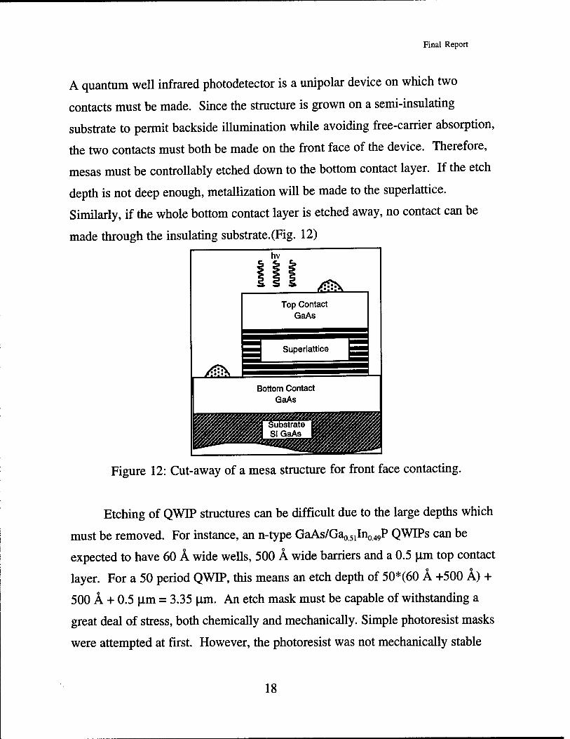
A quantum well infrared photodetector is a unipolar device on which two
contacts must be made. Since the structure is grown on a semi-insulating
substrate to permit backside illumination while avoiding free-carrier absorption,
the two contacts must both be made on the front face of the device. Therefore,
mesas must be controllably etched down to the bottom contact layer. If the etch
depth is not deep enough, metallization will be made to the superlattice.
Similarly, if the whole bottom contact layer is etched away, no contact can be
made through the insulating substrate. (Fig. 12) hv
Top Contact GaAs
Superlattice
Bottom Contact GaAs
Figure 12: Cut-away of a mesa structure for front face contacting.
Etching of QWIP structures can be difficult due to the large depths which
must be removed. For instance, an n-type GaAs/Gao51In049P QWIPs can be
expected to have 60 Ä wide wells, 500 Ä wide barriers and a 0.5 um top contact
layer. For a 50 period QWIP, this means an etch depth of 50*(60 Ä +500 A) +
500 A + 0.5 u,m = 3.35 urn. An etch mask must be capable of withstanding a
great deal of stress, both chemically and mechanically. Simple photoresist masks
were attempted at first. However, the photoresist was not mechanically stable
18

Final Report
enough on its own to resist a long selective etch in mineral acids. Silicon Dioxide
grown by either Plasma Enhanced Chemical Vapor Deposition (PECVD) or
Electron Beam Evaporation (E-beam) proved to be much more resistant to
undercut. However, pinholes are formed in the evaporation process which allow
undesired etching of the mesas. Moreover, the metallization step can then fill
these etched holes and short out the mesas. The solution to the etch mask problem
was to use both photoresist and Si02. The silicon dioxide provides the strength
and the photoresist fills the pinhole. The probability of undesired etching of the
mesas is thus greatly reduced. Therefore, the procedure for obtaining the etching
mask is as follows: (i) deposition of an Si02 layer over the whole sample area,
(ii) photolithography to define square patterns of photoresist, and (iii) etching of
the Si02 layer using a buffered hydrofluoric acid solution. Typically, 400 (im x
400 |im mesas are used for evaluation of single element QWIPs.
In conventional GaAs/A^Ga^As QWIPs, mesas can be wet chemically etched
using a non-selective etchant such as 1 H3P04: 1 H202: 8 H20, which provides
a controllable etch rate of about 0.8 ^m/min. for both GaAs and AlxGai.xAs. In
GaAs/Gao51Ino49P heterostructures, we have investigated non selective etchants
based on H2S04: H202: H20 and Br2: MeOH. In both cases, the etch rate was
difficult to control because of the difference in the etch rate of GaAs and
GaosJn^P (Gao51In049P is much slower than GaAs). Therefore, a fully selective
etching procedure was investigated. 1 H3P04: 1 H202: 10 H20 (1:1:10) was
used as the GaAs etchant, and undiluted HC1 was used as the GalnP etchant. Both
etchants are highly selective. The top GaAs contacts layer were first removed by
the phosphoric acid-based etch. The superlattices were then etched away by
successive etches in the following manner:
1. 20 seconds in HC1 (barrier etch or GaosJno^P etch)
2. 10 seconds of deionized water rinse
19

Final Report
3 20 seconds in 1:1:10 (well etch or GaAs etch)
4 10 second of deionized water rinse
This procedure was found to be highly controllable and reproducible for
GaAs/ Gao51In0.49P superlattices. Upon mesa etching, the Si02 + photoresist etch
mask is removed by soaking the sample into concentrated HF which etches the
Si02 layer and lifts off the photoresist layer.
Following mesa etching and mask removal, two metallization techniques have
been used successfully. These procedures had been developed and optimized for
aluminum-free high power lasers. The first technique consists in the deposition
of Au/AuZn/Au by thermal evaporation over the whole sample area. Following
the evaporation, the sample is then pre-annealed at a temperature of 330 C under
a flow of forming gas (a mixture of 10% hydrogen in nitrogen) for 2-3 minutes
in order to improve the adhesion of the metallization layer. 100 urn x 100 um
photoresist squares are then patterned at the top and bottom of the etched mesas
using standard photolithography procedures. The Au/AuZn/Au is then etched
away using a KI: I2: H20 solution, and the photoresist mask is then dissolved
in acetone. The Au/AuZn/Au metallization is then annealed at 440 C under
forming gas for 2-3 minutes.
Figure 13 shows a top view of 4 mesas after etching and metallization.
Once the samples were fully processed, individual chips were cleaved off and
mounted onto copper heat sinks. Here again, the mounting procedure was
derived from previous developments and optimizations performed for high
power lasers, except the mounting requirements are far less stringent for QWIPs.
The chips were indium-bonded to copper heat sinks, and connections were made
using a ball-bonder apparatus equipped with 25 um diameter gold wire.
20

Final Report
Since the goal of the initial series of samples was to demonstrate very long
wavelength detection, the photoresponse spectrum is the most critical
measurement of the performance of these devices.
-aaB-BB B Bi Bi
Bi Bi B Bi Bi
1 ■ a ■
___________ a B a
B ai BI B
B BI aa B
BI Bi Bi
B ai ai a Bi Bi Bi
a Bi as a
B BI ai a ai ai ai
Bi Bi Bi
a a a ■ a a i
at Bi BB B ai ai a Bi Bi Bi
Bi Bi Bi
a Bi ai a Bi Bi Bi
B ai ai a
B BI SI B Bi Bi aa
B B B
a a B I « B ■ B a a
a a a
I B B ■ a a a
a Bi at B B a a ■ ■ B 1
B Bi Bi ■ Bi Bi Bi
B Bi Bi a
a BI BI at
Bi Bi Bi B Bi Bi B a a a
a a a a at M a a a a
a at ai a a a a
B ai a> a a a a
Bi BI Bi
■ BI
I i ■ _________
" " "_"_■ "_"_"_■_■-"_"_"_■_
■ 1 1 IB!
i ■ BBBBBBBBBBB
■ Metalized EJ
Contact E C
BI ai
cpose ottor onta<
D d Top n Contact :t
Figure 13: Top view of etched sample
The responsivity wavelength spectra R(l) of the samples was measured at normal
incidence using a Mattson Fourier-transform infrared (FTIR) spectrometer. The
spectrometer uses a pyroelectric detector which has a flat response over the range
of 2 to 25 Jim. The normalized responsivity spectra R(k) for three samples is
shown in Fig. 14. These samples clearly demonstrate the high controllability and
accuracy of the MBE grown QWIPs even for very long wavelengths. Table 4
contains the measured values of peak Xp and cutoff Xc wavelength, full width half
maximum (AA,), as well as the peak responsivity values. Figure 15 shows the
peak wavelength plotted against the well width and Figure 16 shows the normal
incidence responsivity versus bias.
21

Final Report
1.0
40angstoms Xp= 104 um
67 angstoms 75 angtroms X ^Zttymji. = 13.3 um
0.8
0.6
0.4
0.2
0.0 i i
10 15
Wavelength (um)
20 25
Figure 14. Normalized Optical Response at 77K
Table 4. Peak responsivities in AAV (at -4 V and 78K) for the different
samples as well as the peak and cutoff wavelengths and FWHM AX (in AX
and meV)
Sample 1 2 3
\ 10.4 12.78 13.3
K 13.4 14.85 15.34
Ak 6p.m 4.25|lm 4.1 urn
185 meV 37 meV 42meV
Rp(£JW) 0.002 0.04 0.07
22

Final Report
A, (um)
30 40 50 60
Well width (Ä)
Figure 15. Peak wavelength as a function of well width.
Normal Incidence Responsivity
R(mA/W) 30
—T" -3
-T- •4
Bias(V)
Fig. 16 Peak normal incidence responsivity vs. bias for the different samples.
The dark current iD play a crucial roll in determining the ultimate performance
of the individual detectors in the array. Therefore, detailed measurements of the
23

Final Report
temperature dependence of the dark current versus voltage were made using a
cold shield that completely surrounded the QWIP and had the same temperature.
Figure 17 shows the temperature dependence of the dark current-voltage curve
for sample 2. For this sample, thermionic emission is the dominant carrier
mechanism down to ~ T=-30K, which is evident by the exponential decrease of
the dark current with temperature.
(A)
Figure 17. Current-voltage (I-V) curve for sample 2 at different
temperatures.
In order to more clearly observe the exponential dark current behavior with bias
and temperature, the date was replotted as a function of 1/T for different biases.
This is shown in figure 18 for sample 2. It is evident that for low biases up to -3
V and high temperatures, thermal activation determines the dark current due to
the thermionic emission of electrons from the well. This region is represented by
the straight line in the plot of log(ID) vs 1/T down to T = 40K. The flat part of
24

Final Report
the curve is due to the onset of tunneling, (which occurs at T < 40 K). At low
bias (where tunneling is negligible) the dark current is expected to increase
exponentially with temperature following:
( AE\ Texp
kT
with the thermal activation energy given by AE=EC - Ep, where k is Boltzmann's
constant and T is the absolute temperature in Kelvin. In order to examine this
dependence in detail, the current-voltage curves of all three samples were
replotted in Figure 19 for Vb = -0.1 V as log (IJT) vs. 1/kT. As expected, the
1000/T[1/K]
Figure 18. Dark current vs. inverse temperature of sample 2 for different
bias, the straight lines represent the thermally activated dark current while
the leveling off at low temperature in due to tunneling.
25

Final Report
normalized dark current log (1,/r) plotted against inverse temperature follows an
excellent straight line for all the sample and from the slop of this line we
determine AE.
1/kT [eV]
Figure 19. Normalized dark current (A/K) versus 1/kT showing the thermal
activation of the dark current.
Based on the responsivity measurements discussed above, the cutoff
wavelength A,c was determined for each sample and the corresponding cutoff
energy Ec determined from Ec = he A,c where h is Planck's constant and c is the
speed of light. The Fermi level Ep of the two dimensional electron gas in the well
can be obtained from:
ND=n0\n(eEF,kT-l)
and
26
Final Report
n =m*kT/7üh2L w
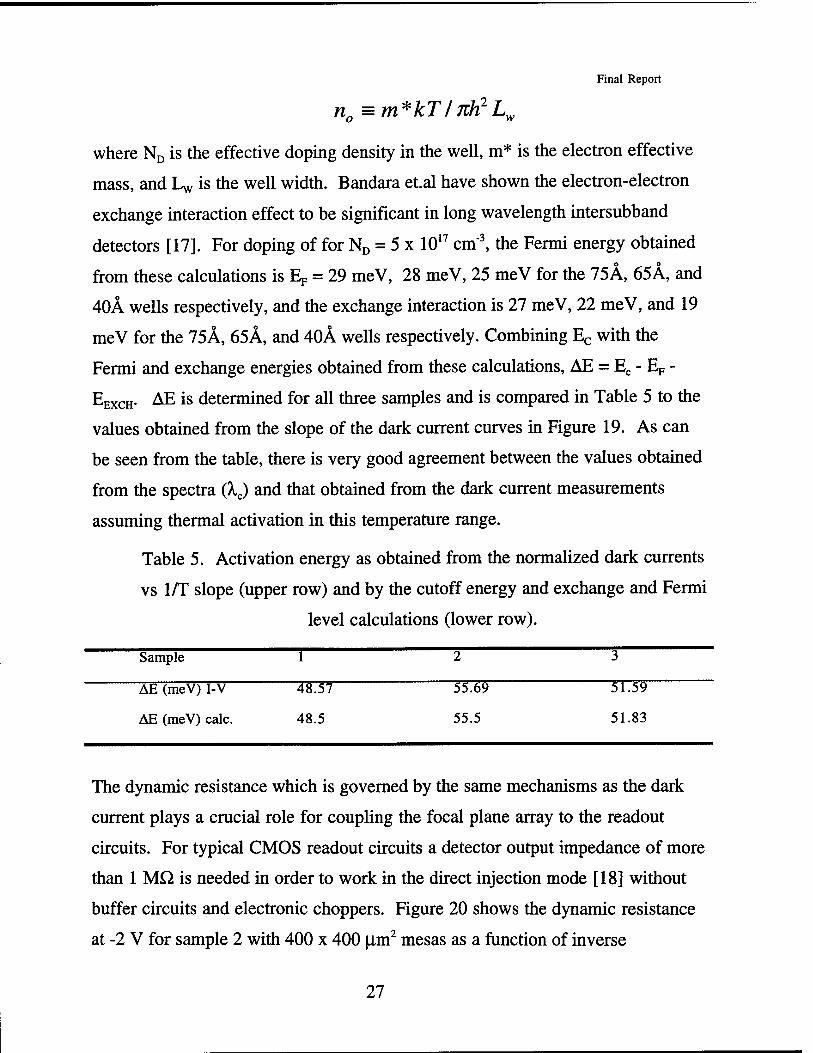
where ND is the effective doping density in the well, m* is the electron effective
mass, and L^ is the well width. Bandara et.al have shown the electron-electron
exchange interaction effect to be significant in long wavelength intersubband
detectors [17]. For doping of for ND = 5 x 1017 cm'3, the Fermi energy obtained
from these calculations is Ep = 29 meV, 28 meV, 25 meV for the 75Ä, 65Ä, and
40Ä wells respectively, and the exchange interaction is 27 meV, 22 meV, and 19
meV for the 75Ä, 65Ä, and 40Ä wells respectively. Combining Ec with the
Fermi and exchange energies obtained from these calculations, AE = Ec - Ep -
EEXCH. AE is determined for all three samples and is compared in Table 5 to the
values obtained from the slope of the dark current curves in Figure 19. As can
be seen from the table, there is very good agreement between the values obtained
from the spectra (kc) and that obtained from the dark current measurements
assuming thermal activation in this temperature range.
Table 5. Activation energy as obtained from the normalized dark currents
vs 1/T slope (upper row) and by the cutoff energy and exchange and Fermi
level calculations (lower row).
Sample 1 2 3
AE (meV) 1-V 307 5H>§ H759
AE(meV)calc. 48.5 55.5 51.83
The dynamic resistance which is governed by the same mechanisms as the dark
current plays a crucial role for coupling the focal plane array to the readout
circuits. For typical CMOS readout circuits a detector output impedance of more
than 1 MQ is needed in order to work in the direct injection mode [18] without
buffer circuits and electronic choppers. Figure 20 shows the dynamic resistance
at -2 V for sample 2 with 400 x 400 Jim2 mesas as a function of inverse
27

Final Report
temperature (1/T). As with the dark current a straight line is evident for
temperatures above 50K. The effect of tunneling can be seen by the tendency
towards saturation at low temperatures. It can be seen that 1 MQ and higher
output impedances can be achieved by cooling the sample to ~ 60K. In this
temperature range most of the Si based multiplexors can work without any
modification in a direct injection mode.
Figure 20. Dynamic resistance vs. reciprocal temperature at -0.5 V for sample 2.
The noise was measured at 80K using an EG&G lock-in amplifier. The noise was
measured under dark conditions (i.e. a cold shield surrounding the QWIP). Since
at 80K the samples are not BLIP, the dominant noise mechanism is shot noise.
Figure 21 shows the bias dependent shot noise at 80K for sample 3.
28

Final Report
80-
60-
40-
Chopping Frequency: 100 Hz Time Constant = 1 ms Corresponding Bandwidth = 250 Hz
hfoiiie ( pA/sqrt(H:
-r 0 -1 -2 -3
Bias (V)
Figure 21. Noise current measured for sample 2.
The noise gain of the device at these temperatures can be calculated from
the noise current and the dark current of the device at that temperature, using the
following equation:
h=WfiW where Id is the dark current of the device, G is the noise gain, and Af is the
bandwidth. For a sufficiently high bias , the quantum well capture probability pc
will be « 1, so that the ratio of the noise gain to the photoconductive gain can be
assumed to be unity[19]. Hence the measured gain from this noise measurement
is also the photoconductive gain. As expected, the noise increases superlinearly
with bias. The optical gain was determined from the noise and dark currents as a
function of bias. . Figure 22 shows the bias dependent optical gain at 80K for
sample 3. The gain increases with bias, with a plateau at -1.5 V at gain = 0.25,
29

Final Report
and then increases rapidly with the bias. For a 20 period superlattice structure,
gain of 0.25 is equivalent to a hot electron mean free path of 5 QW periods, i.e.
around 3500Ä, and therefore corresponds to a capture probability of pc=0.2. For
V> 2 V, the superlinear increase in gain is due to avalanche multiplication of the
high energy electrons.
0.6
0.5-
0.1 -
Bias (V)
Figure 22. Optical gain, determined from the measured dark current noise for
sample 3.
The responsivity of the detector can be expressed in terms of its quantum
efficiency ( h ) and gain G as:
R(X) = r]G qX he
30

Final Report
From this equation, a quantum efficiency of 1.3% is calculated for sample 3 using
values at -2.5V: gain = 0.50, R(A.) = 0.072 AAV, and Xp = 13.3 urn.
Combining the responsivity values and the noise currents, the specific detectivity
D* can be obtained from:
R D*=-^-4W
Figure 23 shows the bias dependence of D* for sample 3 at 80K. D* increases
with bias up to -0.75V, and then saturates. Although the responsivity continues to
increase with bias at higher voltage, the noise also increases and so the detectivity
remains constant.
109-a
108 -.
D(cmHz/W) 107 J
106 T
105-
104JT 1 1 1 1 1 1 1 1 ' 1 ■ 1 " 1 ■ 1 ■ 1 0.0 -0.5 -1.0 -1.5 -20 -2.5 -3.0 -3.5 -4.0 -4.5
Bias (V)
Figure 23. Detectivity (D*) as a function of bias for sample 3 at 80K.
31

Final Report
Several favorable comparisons can be made between these preliminary detectors
and AlGaAs detectors already published in the literature.
Table 7. Comparison of GalnP and GaAlAs QWIPs.
Value GalnP/GaAs AlGaAs/GaAs AlGaAs/GaAs
sample 2 ref. Levine JAP 76 1994
ref. Levine JAP 70 1991
J^ [^lA/cm'] 1875^A/cmx 2546 nA/cm' 3183 nA/cm'
at -IV, 50K
Gain (-1.5V, 77K)
0.25 0.1 .065
The detectivity of these preliminary samples, which were not optimized,
also compares well with the expected values for detectivity as a function of cutoff
wavelength. In summary, in this study experimental results characterizing
GalnP/GaAs -based very long wavelength quantum well infrared photodetectors
in the 10-15 jxm spectral range have been presented. As was emphasized
throughout the work, these were preliminary experiments intended to show the
opportunity for GaIn(As)P/GaAs QWIPs to be used instead of AlGaAs/GaAs
QWIPs for long wavelength photodetectors. Further optimization of these
GalnP/GaAs detectors is necessary, in addition to the growth and fabrication of
GalnAsP/GaAs QWIPs for even longer cutoff wavelengths.
32

Final Report
References
1. J.Y. Andersson, J. Appl. Phys. 78, 6298 (1995).
2. B.A.Wilson, IEEE J. Quantum Electron. 24, 1763 (1988).
3. P.Ho, et.al. Appl. Phys. Lett. 62, 93-95 (1993).
4. M. Razeghi, MOCVD Challenge vol 1. IOP publishers, 1989.
5. M.Razeghi, MOCVD Challenge vol 2 IOP publishers, 1995.
6. M. Razeghi, Nature 369 631(1996).
7. Garbuzov et.al. IEEE J. Quantum Electron. QE-27 1531.
8. J.M. Olson et.al. Appl. Phys. Lett. 56, 623 (1990).
9. W.C. Mitchel et.al. Appl. Phys. Lett. 65, 1578 (1994).
10. M. Razeghi et.al. Appl. Phys. Lett. 55, 457 (1989).
11. B.F.Levine et.al. Appl. Phys. Lett. 58, 1551 (1991).
12. J. Hoff et. al. Appl. Phys. Lett. 67, 22 1995.
13. J. Hoff et. al. Appl. Phys. Lett. 78 2126 1995.
14. J. Hoff et. al. Superlatt.&Microstruc.l8, 249 (1995)
15. J. Hoff et. al. SPIE Proc. 2685, 62 (1996)
16. S. Gunapala, et. al. Appl. Phys. Lett. 57, 1802 (1990)
17. K. Bandara, et. al. Appl. Phys. Lett. 53, 1931 (1988)
18. B. F. Levine, et. al. J. Appl. Phys. 76, 6004 (1994)
19. B. Xing et. al. J. Appl. Phys. 76, 1889 (1994)
33