The Analysis and Compensation of Dead-time Effects in PWM Inverters
PWM for Active Thermal Protection in Three Level Neutral Point Clamped Inverters The-Minh Phan
1, Nikolaos Oikonomou
2 , Gernot J. Riedel
2, Mario Pacas
1 .
[email protected]; [email protected]; [email protected]; [email protected] .
1 Professorship for Power Electronics and Electrical Drives, University of Siegen, Germany.
2 ABB Corporate Research, Baden-Daettwil, Switzerland.
Abstract—For high power applications, in which the discrete power switches are mounted on separate heatsinks, an overload of a semiconductor device leads to a local excessive thermal stress and eventually to a failure of the system. Despite of several control strategies that ensure the even distribution of losses in the normal operation, a local thermal overload can arise due to degradation of the cooling system, inappropriate placing of the semiconductor device, failures in the electronics, etc. In this paper, a new fault tolerant control approach to deal with this matter is introduced and verified by measurements on a laboratory setup. When detecting increased thermal stress of one IGBT module, the switching strategy is altered in order to reduce the thermal load of that particular module and to redistribute the heat from the affected group or valve to the other switches. Hence, the temperature of the stressed module is kept under the critical limit and the thermal overload is reduced. In this way the reliability and the lifetime of the converter is maximized even in case of thermal overload. In the proposed novel modulation concept, the balancing of the neutral point potential of the 3L-NPC Inverter is also ensured without any additional hardware.
Keywords—Fault tolerant control, space vector PWM, active lifetime extension (ALE).
I. INTRODUCTION
In the following, a Three-Level Neutral Point Clamped Voltage Source Converter (3L-NPC VSC) [1] is assumed. In this topology, the redundant space voltage vectors are typically used for the balancing of the neutral point or for the reduction of the common mode voltage. Their utilization for reduction of the losses in the semiconductor devices was first mentioned in [2]. The approach presented there, takes advantage of the redundant space voltage vectors to actively redistribute losses from an overheated semiconductor device to the other cooler devices; hence, the possibility of a system failure is avoided. Moreover, as a long term effect, the expected lifetime of the stressed components is significantly extended because the devices are protected against excessive thermal load. Therefore this strategy was named ALE (active lifetime extension). As the neutral point voltage has to be controlled also by using the same space voltage vector redundancies, a trade-off between the loss redistribution
concept and the neutral point control mechanism is needed to ensure the proper function of the system.
The modulation scheme presented in the following is used to increase the lifetime of one overheated device. After detection of an excessive thermal stress in a switch, the system goes into a fault tolerant control mode. Hereby, the redundancies of the space voltage vectors in the multilevel inverter are exploited. Therefore, this concept is different to the proposals in [3][4][5] where the target is the uniform distribution of the thermal losses under normal operation. There the topology of the 3L-NPC VSC is modified by adding IGBTs parallel to the neutral point diodes. Thanks to these complementary switches, 4 additional redundant states are obtained for the connection of a given output phase to the neutral point. These redundancies are then utilized to improve the thermal performance and for obtaining a uniform distribution of the losses among the switches. It is important to mention, that the original 3L-NPC VSC does not have any redundancies for the switching states 0. Hence, the approach and the target of ALE are completely distinct to those works [3][4][5].
In [6] a method for the thermal redistribution under the low-voltage, ride-through conditions is presented that is similar to the proposal of the present work. There the inverter is operated in the low modulation range while the current is reactive and the redundant states of the zero space vector are used to relocate the losses. The control scheme described in the following takes also advantage of the redundant states but in difference to [6] not only the redundant zero space vectors but all the redundancies of the 3L-NPC VSC are taken into account and the control is designed for the operation in the whole modulation and current range of the inverter.
As stated before, the redundancies of a 3L-NPC VSC can be used for balancing the neutral point, for the reduction of the common mode voltage or like in the present case for the redistribution of the losses but not all these targets can be achieved at the same time. The solution presented here increases the lifetime of the overheated device at the expense of increased ripple of the potential of the neutral point. This
978-1-4799-5776-7/14/$31.00 ©2014 IEEE 3710
is for sure a drawback that can be tolerated for the relatively short duration that is required to fix the thermal overload.
Although ALE is intended to be used in the whole modulation range, the modulation strategy is different in the low and in the high modulation range, hence its analysis and validation are separated for both regions of operation. In a previous paper [7] the ALE for the operation in the region of higher voltages and modulation index was explained and only validated by simulation. In the meanwhile, the experimental setup was completed and the experimental results presented here corroborate the theoretical approach.
The ALE strategy in the low modulation range is possible as well and was analyzed and verified by simulation and experiments but is outside of the scope of this paper and will be presented in a future work.
II. STRATEGY FOR LOSS REDISTRIBUTION IN 3L-NPC
VSC WITH SPACE VECTOR MODULATION
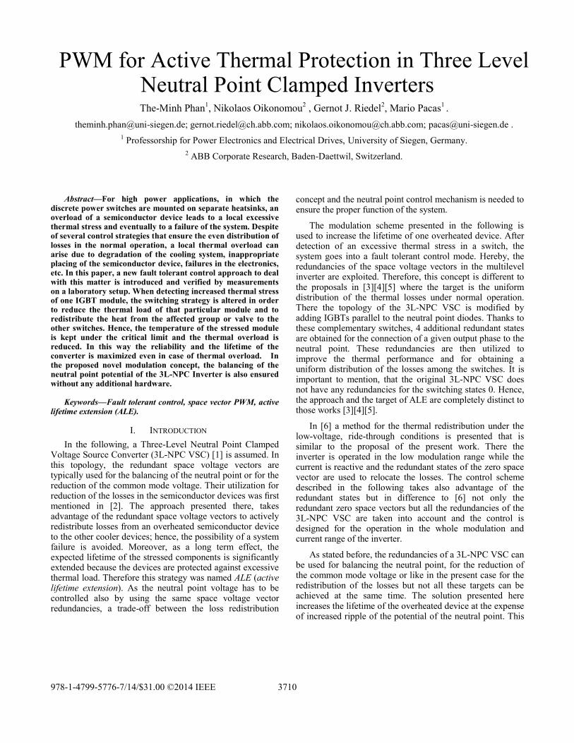
For a basic analysis, it is sufficient to consider the upper leg of phase U of the inverter depicted with red color in Fig. 1 as the stressed device, in which the thermal load has to be reduced. The modulation index m (0 ≤ m ≤ 1) is defined as:
√
(1)
where is the amplitude of phase voltage and Udc is
the dc voltage of the 3L-NPC inverter.
As already explained the present paper focuses only on the operation of the inverter in the higher modulation range 0.5 < m ≤ 1, in a following work the range 0 < m ≤ 0.5 will be considered.
Figure 1. 3L-NPC VSC, in red the devices with higher thermal load
A. Reduction of losses by using redundant space voltage vectors
The thermal losses of a semiconductor device consist of switching- and of conduction losses. Since the realization of the modulation affects these losses in a different way, the two different types of PWM according to [8] will be distinguished: a continuous and discontinuous one. The discontinuous modulation is more convenient regarding the
losses, therefore in the following the effect of the redundant space voltage vectors on switching and conduction losses are only considered for the discontinuous PWM and for the proposed ALE-modulation.
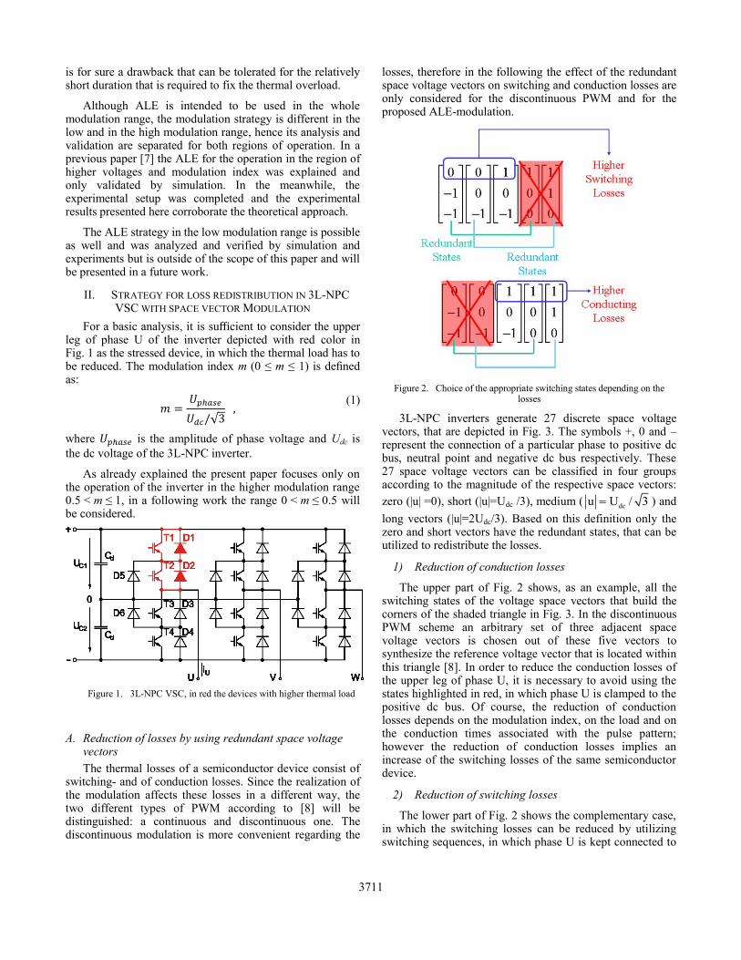
Figure 2. Choice of the appropriate switching states depending on the losses
3L-NPC inverters generate 27 discrete space voltage vectors, that are depicted in Fig. 3. The symbols +, 0 and – represent the connection of a particular phase to positive dc bus, neutral point and negative dc bus respectively. These 27 space voltage vectors can be classified in four groups according to the magnitude of the respective space vectors:
zero (|u| =0), short (|u|=Udc /3), medium ( dcu U / 3 ) and
long vectors (|u|=2Udc/3). Based on this definition only the zero and short vectors have the redundant states, that can be utilized to redistribute the losses.
1) Reduction of conduction losses
The upper part of Fig. 2 shows, as an example, all the switching states of the voltage space vectors that build the corners of the shaded triangle in Fig. 3. In the discontinuous PWM scheme an arbitrary set of three adjacent space voltage vectors is chosen out of these five vectors to synthesize the reference voltage vector that is located within this triangle [8]. In order to reduce the conduction losses of the upper leg of phase U, it is necessary to avoid using the states highlighted in red, in which phase U is clamped to the positive dc bus. Of course, the reduction of conduction losses depends on the modulation index, on the load and on the conduction times associated with the pulse pattern; however the reduction of conduction losses implies an increase of the switching losses of the same semiconductor device.
2) Reduction of switching losses
The lower part of Fig. 2 shows the complementary case, in which the switching losses can be reduced by utilizing switching sequences, in which phase U is kept connected to
3711

the positive dc bus and by avoiding the states marked in red. By favoring these sequences, it is obvious that the conduction losses increase due to longer on-time duration of the corresponding switch.
3) Choice of the appropriate approach
As explained above, this strategy exhibits concurrent targets and leads therefore to a dilemma as the reduction of the conduction losses leads to higher switching losses and vice versa. Thus, the consideration of other aspects is mandatory. The operation of the inverter at higher output voltages yields switching sequences, in which the on-time of the short vectors decreases with increasing modulation index. The reduction of conduction losses by exploiting the corresponding redundant states is therefore limited at high values of the modulation index. In contrast to this, the reduction of the switching losses is independent from the on-times of the redundant states in the corresponding sequences. Furthermore the switching losses in power semiconductor devices for medium voltage applications are particularly high. Hence, the reduction of switching losses is preferred in this region of operation regardless of the higher conduction losses. As shown in the next sections a reduction of the overall losses can still be achieved with this strategy for a wide operation range.
B. Trade-off between neutral point balancing and
distribution of losses by using redundant voltage space
vectors
As already explained, the neutral point balancing and the redistribution of losses are concurrent optimization targets demanding both the utilization of redundant states of the inverter. The optimization problem is particularly challenging in the higher modulation range, where the availability of redundant states decreases. Therefore, this paper proposes a viable solution for the arbitration of this conflict. Fig. 3 shows the blue area where the ALE strategy for the redistribution of losses is applied to the upper leg of phase U. When the reference space vector of the output voltage is located in this area and a thermal overload in the upper leg of phase U occurs, the ALE control is initiated and has priority besides the control of neutral point voltage is deactivated. While the ALE control is active, the neutral point is continuously monitored and in case that its potential crosses a predefined threshold, the priority of ALE is withdrawn and the neutral point control is reactivated. If the threshold is chosen to low, the ALE control is interrupted too often and its effectiveness is diminished. In the case the threshold is too high; the balancing of the voltage on the dc-link capacitors is affected leading to a deteriorated quality of the output voltage waveforms as well as to an increased voltage stress on the switching devices. The level of the threshold depends on the load and also on the installed capacitance in the dc-link as the drift of neutral point is smaller for the larger dc-link capacitors. Thus, a compromise in defining the threshold is always necessary.
If the reference space vector of the output voltage is located within the white colored regions in Fig.3 the control
of the neutral point takes priority over ALE. For the yellow regions of Fig. 3 the ALE-control is different and will be treated in a future work.
Figure 3. Operation map for the ALE
C. Starting of the ALE-control
In the case that the temperature of the heat sink of a device exceeds the permissible limit because of thermal overload, the first action to be taken is switching the control of the inverter from continuous PWM to discontinuous PWM mode to reduce the switching losses. If this is still not sufficient to keep the temperature of the particular device within the safe zone of operation, the ALE approach is then applied for a further reduction of the thermal losses and of its temperature.
III. RESULTS
A. Simulation results
To verify the proposed modulation scheme, a case study of a medium voltage induction machine (Un = 3000 V, Pn = 560 kW) fed by a 3-level NPC inverter (Udc = 4670 V, Cdc = 3.8 mF, switching frequency = 1000 Hz) was investigated by means of simulation for rated operation with m = 0.97 and cosφ = 0.84. The numbering rule for the semiconductors devices is as shown in Fig. 1. The calculation of the losses in the simulation was carried out in the way explained in [7],[9] and [10] and for IGBTs with data according to [12].
Fig. 4 shows the conduction losses of all IGBT switches for three different cases: the blue columns represent the values for normal operation with continuous PWM (C-PWM), the green ones for normal operation with discontinuous PWM (D-PWM) and the red ones for ALE operation. The grey columns on the top of all other columns show the corresponding switching losses in each particular operation mode.
3712
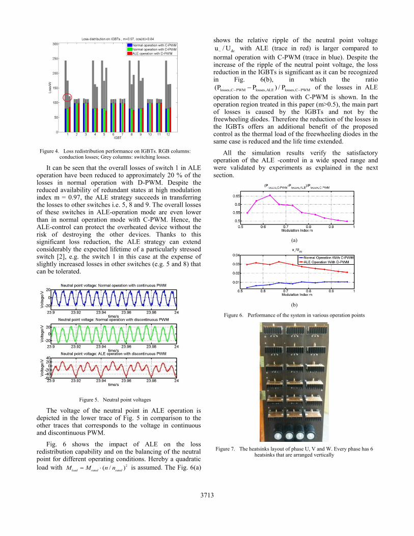
It can be seen that the overall losses of switch 1 in ALE operation have been reduced to approximately 20 % of the losses in normal operation with D-PWM. Despite the reduced availability of redundant states at high modulation index m = 0.97, the ALE strategy succeeds in transferring the losses to other switches i.e. 5, 8 and 9. The overall losses of these switches in ALE-operation mode are even lower than in normal operation mode with C-PWM. Hence, the ALE-control can protect the overheated device without the risk of destroying the other devices. Thanks to this significant loss reduction, the ALE strategy can extend considerably the expected lifetime of a particularly stressed switch [2], e.g. the switch 1 in this case at the expense of slightly increased losses in other switches (e.g. 5 and 8) that can be tolerated.
Figure 5. Neutral point voltages
The voltage of the neutral point in ALE operation is depicted in the lower trace of Fig. 5 in comparison to the other traces that corresponds to the voltage in continuous and discontinuous PWM.
Fig. 6 shows the impact of ALE on the loss redistribution capability and on the balancing of the neutral point for different operating conditions. Hereby a quadratic
load with 2( / )
load rated ratedM M n n is assumed. The Fig. 6(a)
shows the relative ripple of the neutral point voltage
~ dcu / U with ALE (trace in red) is larger compared to
normal operation with C-PWM (trace in blue). Despite the increase of the ripple of the neutral point voltage, the loss reduction in the IGBTs is significant as it can be recognized in Fig. 6(b), in which the ratio
losses,C PWM losses,ALE losses,C PWM(P P ) / P of the losses in ALE
operation to the operation with C-PWM is shown. In the operation region treated in this paper (m>0.5), the main part of losses is caused by the IGBTs and not by the freewheeling diodes. Therefore the reduction of the losses in the IGBTs offers an additional benefit of the proposed control as the thermal load of the freewheeling diodes in the same case is reduced and the life time extended.
All the simulation results verify the satisfactory operation of the ALE -control in a wide speed range and were validated by experiments as explained in the next section.
(a)
(b)
Figure 6. Performance of the system in various operation points
Figure 7. The heatsinks layout of phase U, V and W. Every phase has 6 heatsinks that are arranged vertically
Figure 4. Loss redistribution performance on IGBTs. RGB columns: conduction losses; Grey columns: switching losses.
3713

(a) Firing pulses of IGBTs with D-PWM (time 10ms/div, voltage 10V/div)
(b) Firing pulse of IGBTs with ALE (time 10ms/div, voltage 10V/div)
(c) Neutral point voltage with D-PWM (time 10ms/div, voltage 30V/div)
(d) Neutral point voltage with ALE (time 25ms/div, voltage 30V/div)
(e) Spectrum of the ripple of Uc1 with D-PWM, (frequency 12.5 Hz/div, amplitude 20db/div)
(f) Spectrum of the ripple of Uc1 with ALE, (frequency 12.5 Hz/div, amplitude 20db/div)
(g) Spectrum of phase current with D-PWM (frequency 12.5 Hz/div, amplitude 20db/div)
(h) Spectrum of phase current with ALE ( frequency 12.5Hz/div, amplitude 20db/div
Figure 8. Electrical performance by m = 0.9, Udc = 350V and 60% rated current of inverter
B. Experimental results
1) The experimental set-up
In order to verify the concept experimentally, the complete control including the space vector modulation was implemented by means of a floating point DSP (TMS320F28335). For the power part a 3L-NPC inverter with a rated current of 50 A was especially designed with 18 separated heatsinks, i.e. 6 heatsinks per phase; they are shown in Fig. 7. Each heatsink is equipped with a
temperature sensor (Pt1000), so that the temperature and, in this way, the heat distribution among the semiconductor devices can be easily investigated. The IGBTs utilized in the downsized laboratory set-up have characteristics for optimized conduction losses [13], therefore they can replicate in a suitable way the thermal behavior of the high power IGBTs. The 3L-NPC VSC is feed a 15 kW induction motor that drives a load emulated by a 21 kW field-oriented controlled motor drive. The inverter under test is operated with a field orientated control scheme and is switched with a
3714

frequency of 5 kHz. The dc-link capacitors have a capacitance of 4.4 mF and the dc-link voltage is 350V.
2) Pulse patterns in ALE operation
The Fig. 8(a) shows the firing pulse of the IGBT number 1 by using discontinuous modulation (D-PWM) for an operating point with m = 0.9 and 60% of the rated current of the inverter. The zone free of pulses in the middle of the pulse pattern is generated by the discontinuous PWM and results in clamping the upper leg of phase U to the positive dc-bus. In case that the ALE-control becomes active the firing pulse pattern of the IGBT 1 changes in such a way that the switching losses are reduced as it is depicted in Fig. 8(b). It is obvious that the effective switching frequency of the IGBT 1 significantly decreases.
The voltage of the neutral point is shown in Fig. 8(c) and in Fig. 8(d) under ALE operation. The waveforms correspond well with the simulation results shown in Fig. 5. The neutral point voltage Unp is defined as:
(2)
the Uc1 and Uc2 refer to voltages of the upper and lower capacitors of the DC link as shown in Fig. 1. The spectrum of the ripple of the capacitor voltage Uc1 in Fig. 8(e) shows a dominant 3rd harmonic component in normal operation. But in the case of ALE, the additional harmonics of 1st, 2nd and 4
th order are present in Fig. 8(f). These effects have
been investigated in the previous works [7],[11]. In any case, regardless of the higher content of harmonics produced by the ALE-control, the amplitude of the neutral point voltage is kept stable within acceptable limits.
The spectrum of the phase current with ALE is depicted in Fig. 8(h) and compared with the current spectrum in normal operation depicted in Fig. 8(g), it shows no significant increase of the harmonics content, hence it is acceptable for the fault tolerant control mode.
3) Thermal performance
Figure 9. Thermal model used for the calculation
Fig. 9 shows the thermal model used for the calculation of the junction temperature of the semiconductor device
based on the losses. The junction temperature is given by Tjuntion = ∆Tjc + ∆Tcs + ∆Tsa + Tambient , the subscripts jc, cs and sa stand for junction-to-case, case-to-heatsink and heatsink-to-ambient temperature drop respectively. Obviously in the steady state the temperature differences are directly proportional to total losses of each semiconductor device. According to this model the temperature difference of heatsink-to-ambient ∆Tsa can be used to estimate the total loss of a particular IGBT including its antiparallel diode, hence Ploss ≈ ∆Tsa, steady-state / Rsa. Hereby Rsa is the thermal resistance of the heatsink. In order to reduce the air convection from the IGBTs that are located in the bottom of the inverter to the ones on the top, that would affect the heat distribution and would eventually lead to an erroneous measurement, every heatsink in Fig. 7 is covered with a small plastic plate preventing in this way the air circulation. The measurement of the temperature of IGBT takes place after reaching the thermal steady state of the whole system, in which no increase of temperature can be registered.
Figure 10. Thermal performance by m = 0.9, Udc = 350V and 60% rated current of inverter
Fig.10 shows the thermal performance for a modulation index m = 0.9, a dc-link voltage Udc = 350V and 60% of the rated current of the inverter. For a better understanding only the most significant values of the losses are plotted for the operation under D-PWM and under ALE. Although different current ratings of IGBTs are investigated in the measurement an in the simulation, both results in Fig. 4 and in Fig. 10 correspond to each other. The losses of the IGBTs 1 have been reduced significantly to expenses of higher losses in the devices number 5, 8 and 9, yet the risk of overheating is kept limited. Since the D-PWM reduces nearly one third of the switching losses as compared to C-PWM, the thermal household is even more favorable.
Fig. 11 shows the performance of ALE in different operation points. The Fig. 11(a) shows the ratio
losses,D PWM losses,ALE losses,D PWM(P P ) / P of the losses of the
examined IGBT Nr. 1 for ALE operation in comparison to D-PWM. A remarkable reduction of the overall losses of at least 12% (m=0.85 and 60% of rated current of inverter) can
3715

be stated. Fig 11(b) and Fig. 11(c) show the ripple of the
neutral point voltage ~ dcu / U for D-PWM and ALE
respectively. The dc-link capacitors in the set-up are intentionally undersized for a better examination of the impact of ALE on the behavior of the neutral point under different operation conditions. Fig. 11(c) shows a clear trend: the higher the load current the larger the neutral point ripples. It can also be recognized that at constant load current the ripple increases with decreasing modulation index. Regarding the negative effects of the ripple on the dc-link capacitors, it can be pointed out that their over temperature stays below 10 K in the ALE operation range. Regardless of the intentional downsizing of the capacitors the ripple on the current flowing into the neutral point does not yield any excessive rise on the temperature. In a commercial 3L-NPC inverter the situation becomes better as the capacitors are properly dimensioned and the effect of the ripple is lessened.
(a)
(b)
(c)
Figure 11. ALE performance in various operation points
There are other options for improving the balancing of the neutral point voltage by limiting the operation map of the ALE strategy depicted in Fig. 3 these investigations are ongoing and outside of the scope of this paper.
In the present stage of development the ALE-strategy allows the fault-tolerant operation of the inverter while accepting a higher harmonic distortion of the output voltage due to the insufficient balancing of the voltage of the neutral point.
IV. CONCLUSION
In this paper, a new concept for the loss redistribution of a 3L-NPC inverter is proposed that aims at the active thermal protection of semiconductor switches which suffer
from overload conditions. The performance of the proposed modulation scheme has been investigated by means of simulations and measurements in a wide operation range with (0.5 ≤ m ≤ 1). This study confirms possibility to redistribute the losses of one selected semiconductor device by using the redundant states of the space voltage vectors. The impact of ALE on the neutral point balancing was also investigated and shows a satisfactory operation when properly applied. The presented concept is also a novel generic approach to redistribute the losses among the phases, which is applicable to any multilevel topology.
REFERENCES
[1] Rodriguez, J.; Bernet, S.; Steimer, P.K.; Lizama, I.E.;, "A Survey on Neutral-Point-Clamped Inverters," Industrial Electronics, IEEE Transactions on , vol.57, no.7, pp.2219-2230, July 2010.
[2] G. Riedel, N. Oikonomou, R. Schmidt und D. Cottet, “Active lifetime extension — Demonstrated for voltage source converters“, Electrical and Electronics Engineers in Israel (IEEEI), 2010 IEEE 26th Convention of , vol., no., pp.000530-000534, 17-20 Nov. 2010.
[3] T. Bruckner, S. Bernet and H. Guldner, “The active NPC converter and its loss-balancing control“.Industrial Electronics, IEEE Transactions on, vol.52, no.3, pp. 855-868, June 2005.
[4] D. Andler, J. Weber, S. Bernet and J. Rodríguez, "Improved model predictive control with loss energy awareness of a 3L-ANPC voltage source converter".Applied Electronics (AE), 2010 International Conference on , vol., no., pp.1-6, 8-9 Sept. 2010.
[5] D. Floricau, E. Floricau and G. Gateau, “Three-level active NPC converter: PWM strategies and loss distribution“. Industrial Electronics, 2008. IECON 2008. 34th Annual Conference of IEEE, vol., no., pp.3333-3338, 10-13 Nov. 2008.
[6] Ke Ma; Blaabjerg, F., "Modulation Methods for Neutral-Point-Clamped Wind Power Converter Achieving Loss and Thermal Redistribution Under Low-Voltage Ride-Through," Industrial Electronics, IEEE Transactions on , vol.61, no.2, pp.835,845, Feb. 2014.
[7] The-minh Phan; Riedel, G.; Oikonomou, N.; Pacas, M., "PWM for active thermal protection in three level neutral point clamped inverters," ECCE Asia Downunder (ECCE Asia), 2013 IEEE , vol., no., pp.906,911, 3-6 June 2013
[8] T. Bruckner and D. Holmes, “Optimal pulse-width modulation for three-level inverters,“.Power Electronics, IEEE Transactions on , vol.20, no.1, pp. 82- 89, Jan. 2005.
[9] M. Bierhoff and F. Fuchs, “Semiconductor losses in voltage source and current source IGBT converters based on analytical derivation“.Power Electronics Specialists Conference, 2004. PESC04. 2004 IEEE 35th Annual, vol.4, no., pp. 2836- 2842 Vol.4, 2004.
[10] R. Schnell, U. Schlapbach, “Realistic benchmarking of IGBT-modules with the help of a fast and easy to use simulation-tool“.PCIM'04 Power Electronics Conference, Nuremberg.
[11] J. Shen, S. Schröder, R. Rösner and S. El-Barbari, “A Comprehensive Study of Neutral-Point Self-Balancing Effect in Neutral-Point-Clamped Three-Level Inverters“.Power Electronics, IEEE Transactions on , vol.26, no.11, pp.3084-3095, Nov. 2011.
[12] HiPak IGBT Module 5SNG 0250P330305
[13] IXYS IGBT, Type IXGR 72N60A3H1
3716