02 PWM Inverters Part II
35
Pulse-Width-Modulated PWM Inverter Part II Cha ter 10 or 6 Pr e ared b Dr . Mohammad Abdul Mannan Assistant Professor, Department of EEE mer can n erna ona n vers y - ang a es
Transcript of 02 PWM Inverters Part II
8/12/2019 02 PWM Inverters Part II
http://slidepdf.com/reader/full/02-pwm-inverters-part-ii 1/35
Pulse-Width-Modulated
PWM Inverter Part IICha ter 10 or 6
Pre ared b
Dr. Mohammad Abdul MannanAssistant Professor, Department of EEE
mer can n erna ona n vers y - ang a es

8/12/2019 02 PWM Inverters Part II
http://slidepdf.com/reader/full/02-pwm-inverters-part-ii 2/35
Current Source Inverter (CSI)
van age o as ompare1. Since the input dc current is controlled and limited, miss
firin of switchin devices or a short circuit would not be
series problems;
2. The peak current of power devices is limited;. e commu a on c rcu s or yr s ors are s mp er;
4. It has ability to handle reactive or regenerative load
without feedback or freewheeling diodes.
Disadvantage of CSI as Compared VSI
1. A CSI requires a relative large reactor (or inductor) to
exhibit current-source characteristics,
2. An extra converter stage is required to control the
,
3. The dynamic response is slower, and
4. Due to current transfer from one pair of switches to
another, an output filter is required to suppress the output
voltage spikes.

8/12/2019 02 PWM Inverters Part II
http://slidepdf.com/reader/full/02-pwm-inverters-part-ii 3/35
Single-Phase Transistorized CSI
e c rcu agram o a s ng e-p ase rans s or ze s s own nFig. 10-36(a).
Since there must be a continuous current flow from the source,
two switches must always conduct – one from upper and onerom ower sw tc es.
The conduction sequence is 12, 23, 34, and 41.
reverse voltage on the transistors.

8/12/2019 02 PWM Inverters Part II
http://slidepdf.com/reader/full/02-pwm-inverters-part-ii 4/35
The gate signals and output current waveshape is shown in
Fi . 10-36 b and c .
When two devices in different arms conduct, the source current
I L flows through the load.
When two devices in the same arm conduct, the source current
is bypassed from the load.rom q. . , e oa
current can be expressed as
∑== ,..5,3,1 sin2sin)( n t nn
nt oi ω π

8/12/2019 02 PWM Inverters Part II
http://slidepdf.com/reader/full/02-pwm-inverters-part-ii 5/35
Single-Phase Thyristorized CSI
e c rcu agram o a s ng e-p ase rans s or ze sshown in Fig. 10-36(a).
1 2 , 1
and C 2 are charged with polarity as shown.
Firin of T and T reverse biases T and T . T and T are
turned off by impulse commutation.
8/12/2019 02 PWM Inverters Part II
http://slidepdf.com/reader/full/02-pwm-inverters-part-ii 6/35
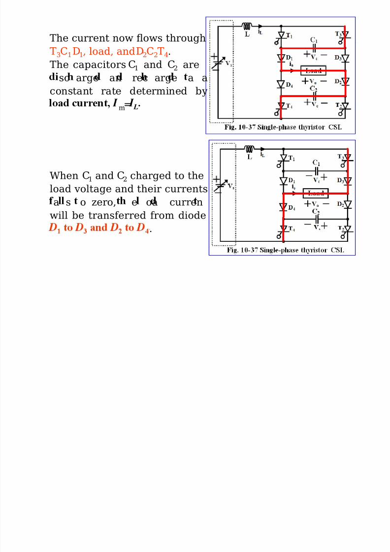
The current now flows through
T 3C 1 D1, load, and D2C 2T 4.The capacitors C 1 and C 2 are
sc arge an rec arge a a
constant rate determined by
= m
When C 1 and C 2 charged to the
load voltage and their currentsa s o zero, e oa curren
will be transferred from diode
.

8/12/2019 02 PWM Inverters Part II
http://slidepdf.com/reader/full/02-pwm-inverters-part-ii 7/35
Firing of T 1 and T 2 reverse
biases T 3 and T 4. T 3 and T 4 are
turned off by impulsecommutation.
The current now flows through
T 1C 1 D3, load, and D4C 2T 2.1 2
discharged and recharged at a
constant rate determined b
load current, I m= I L.
load voltage and their currents
falls to zero, the load currentwill be transferred from diode
D3 to D1 and D4 to D2.
e capac ors are now rea y
to turn off T 1 to T 2.

8/12/2019 02 PWM Inverters Part II
http://slidepdf.com/reader/full/02-pwm-inverters-part-ii 8/35
Three-Phase CSI
. - -current-source inverter.
The wave forms for gating signals
and line currents for a wye-
connected load are shown in Fi .
10-38(b).
At any instant only two thyristors
con uc a e same me. ac
device conducts for 120o.

8/12/2019 02 PWM Inverters Part II
http://slidepdf.com/reader/full/02-pwm-inverters-part-ii 9/35
The current for phase a can be expressed as:
∑∞
=
+=⎥
⎥
⎦
⎤
⎢
⎢
⎣
⎡
,..5,3,1)79.10()
6(sin
6cos
2)(
nt nn
n
L I
t ai π ω π
π
The PWM, or SPWM, or MSPWM technique can be
a lied to var the load current and to im rove the ualit
of its waveform.
The current source inverter (CSI) is a dual of voltagesource inverter (VSI).
The line-to-line of a VSI is similar in shape to the line
.

8/12/2019 02 PWM Inverters Part II
http://slidepdf.com/reader/full/02-pwm-inverters-part-ii 10/35
Filter to Reduced Output Harmonics
o re uce e ou pu armon cs, ou pu ers are necessary.Fig. 10-40 shows the commonly used output filters.
A C -filter is very simple, but it draws more reactive power.
An LC -filter as in Fig. 10-40(b) can eliminate only onerequency.
A properly designed CLC -filer as in Fig. 10-40(c) is more
less reactive power.

8/12/2019 02 PWM Inverters Part II
http://slidepdf.com/reader/full/02-pwm-inverters-part-ii 11/35
Pulse Width Modulated (PWM) Inverter
quare-wave nver ers su ers rom wo ma or raw ac s:(i) The output voltage of the inverter cannot be controlled for a fixed-source
voltage. To achieve voltage control, the inverter must be fed either from
controlled ac-dc or dc-dc converter.
(ii) The output voltage contains appreciable harmonics (low-frequency range).
Also THD is ver hi h.
The problem of square-wave inverter can be minimized by using PWM
technique.
PWM techniques allows:(i) Variation of output voltage within the inverter by varying the gain of the
. .
(ii) Variations of output frequency either by varying the number of pulses per
half-cycle of the output or by varying the period for each half-cycle with fixednum er o pu ses n eac a -cyc e.
(iii) Simultaneous variation of out voltage and frequency is also possible. So
that V/f ratio can be kept constant. This feature is required in induction motor-
drives.
(iv) Control of harmonics at the output of the inverter.

8/12/2019 02 PWM Inverters Part II
http://slidepdf.com/reader/full/02-pwm-inverters-part-ii 12/35
Why the Output Voltage is Required to Control in
The control of output voltage is required in industrial applications for the
following reasons:
• To cope with the variation of dc input voltage,
• For voltage regulation of inverter, and
• For the constant volts/fre uenc control re uirement
In PWM technique the gate signal of switching devices of an inverter is
obtained b com arin a reference si nal with a carrier si nal.
The magnitude of the output voltage depends on the amplitude modulation
index and the frequency of the output voltage depends on the frequency of
.
Thus, the magnitude of output voltage can be controlled by varying the
modulation index and the frequency of output voltage can be controlled by
vary ng e requency o re erence s gna .
8/12/2019 02 PWM Inverters Part II
http://slidepdf.com/reader/full/02-pwm-inverters-part-ii 13/35
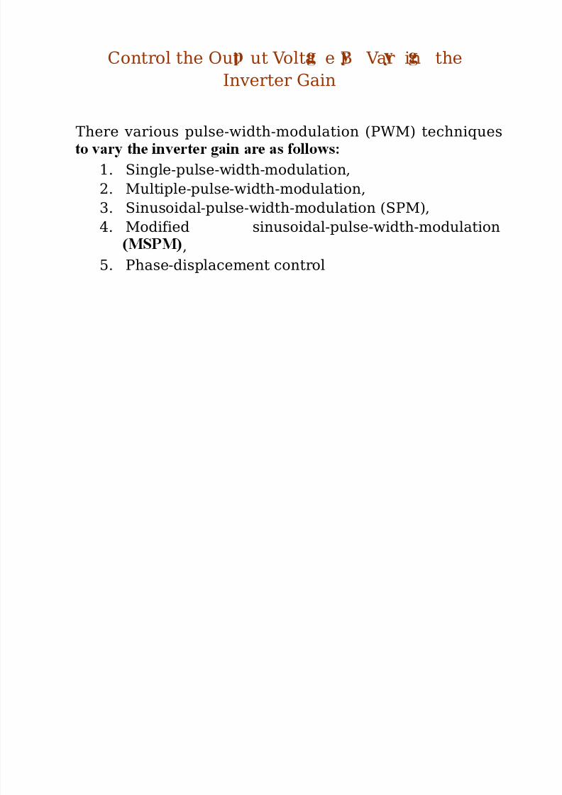
Control the Out ut Volta e B Var in the
Inverter Gain
There various pulse-width-modulation (PWM) techniques
1. Single-pulse-width-modulation,
2. Multiple-pulse-width-modulation,
3. Sinusoidal-pulse-width-modulation (SPM),4. Modified sinusoidal-pulse-width-modulation
,
5. Phase-displacement control

8/12/2019 02 PWM Inverters Part II
http://slidepdf.com/reader/full/02-pwm-inverters-part-ii 14/35
Single-Pulse-Width-Modulation
-is varied to control the inverter output voltage.
The followin fi ure shows the eneration of atin si nals and
output voltage of single-pulse full-bridge inverters.
The gating signals are generated
b com arin a rectan ular
reference signal of amplitude, A r, with a triangular carrier
wave o amp tu e, c.

8/12/2019 02 PWM Inverters Part II
http://slidepdf.com/reader/full/02-pwm-inverters-part-ii 15/35
The frequency of fundamental output voltage is determined by
the fre uenc of reference si nal.
By varying A r from 0 to A c, the pulse width, δ , can be varied
from 0o to 180o.
The ratio of A r to A c is control variable and defined as the
amplitude modulation index.The amplitude modulation index, or simply modulation index
is given by M = A r/ A c.
The rms output voltage can be found from:
2/1
π δ
π
δ π
ω π sV t d sV oV =∫
+
−
=
⎥⎥⎥⎥⎥
⎢⎢⎢⎢⎢
2)(
)(222
The Fourier series of output voltage
ields:∑
==
,..5,3,1sin
2sin)(
nt nn
n
st ov ω
π

8/12/2019 02 PWM Inverters Part II
http://slidepdf.com/reader/full/02-pwm-inverters-part-ii 16/35
Fig. 10-12 shows the harmonic
, .
The dominant harmonic is the
third, and the distortion factor
increases significantly at low
output voltage.
Example [2, p.654] A single-phase full-wave inverter uses
-
third harmonics from the output wave. Determine the width of pulse, .
Solution: From the Fourier series, we obtain the rms value of
third harmonics is:34 δ V 2233 π
To eliminate the third harmonics, V 3 =0, thus 023sin =δ °=180
23δ
°=°×= 12018032δ

8/12/2019 02 PWM Inverters Part II
http://slidepdf.com/reader/full/02-pwm-inverters-part-ii 17/35
Multiple-Pulse-Width-Modulation
each half-cycle of output voltage.
The eneration of atin si nals for turnin on and off of
transistor is shown in Fig. 10-13(a) by comparing a reference
signal with a triangular carrier wave.The frequency of reference signal, f r, sets the output frequency,
f o, and the carrier frequency, f c, determines the number of
- , .
The rms output voltage
modulation index (or
ratio .This type of modulation
is also known as uniform
pulse-width modulation
(UPWM).

8/12/2019 02 PWM Inverters Part II
http://slidepdf.com/reader/full/02-pwm-inverters-part-ii 18/35
The number of pulses per half-cycle is found
from: 22 f
mc f p ==
Where m f = f c/ f o is defined as the frequency modulation ratio
or index . The variation of modulation index M from 0 to 1
varies the pulse width from 0 to π / p and the output voltage
from 0 to V s.If δ is the width of each
pulse, the rms output δ δ π
p p
p =+
= ⎥⎥⎤
⎢⎢⎡
2/12)/(
22vo age can e oun
from: δ π π p− ⎥⎥
⎦⎢⎢
⎣ 2)/(2
The general form of Fourier
series for the instantaneous
∞= sin)( t n Bt v ω
= ,..5,3,1n

8/12/2019 02 PWM Inverters Part II
http://slidepdf.com/reader/full/02-pwm-inverters-part-ii 19/35
If the positive pulse of mth pair starts at ω t = m and ends at
ω t = m+π, the Fourier series coefficient for a pair of pulses is:
⎥⎥⎥⎥⎤
⎢⎢⎢⎢⎡
⎥⎥⎥
⎦
⎤
⎢⎢⎢
⎣
⎡
∫ + ∫ +++−= )(cos)(cos1 δ α α
δ α π α π ω ω ω ω π
mm
mm
t td nt td nnb
⎥⎥⎥
⎦⎢⎢⎢
⎣ ⎥
⎥
⎦
⎤
⎢⎢
⎣
⎡
⎟⎟
⎠
⎞
⎜⎜
⎝
⎛
⎟⎟
⎠
⎞
⎜⎜
⎝
⎛ ++−+=2
sin2
sin2
sin2 δ α π δ α δ
π mnmnnn sV
The coefficient B n can be found by adding the effects of all
pulses:++−+= ⎥
⎤⎢⎡
⎟ ⎞
⎜⎛
⎟ ⎞
⎜⎛
pnnnsV B sinsinsin
2 δ α π δ α δ
= ⎦⎣ ⎠⎝ ⎠⎝
m 1

8/12/2019 02 PWM Inverters Part II
http://slidepdf.com/reader/full/02-pwm-inverters-part-ii 20/35
Advantages(i) Distortion factor are reduced com ared to sin le- ulse-
modulation.
(ii) As value of “p” increases amplitudes of lower harmonicre uces.
Disadvantagesncrease num er o pu ses, sw c ng osses are
increased.

8/12/2019 02 PWM Inverters Part II
http://slidepdf.com/reader/full/02-pwm-inverters-part-ii 21/35
Sinusoidal Pulse-Width-Modulation (SPWM)
proportion to the amplitude of a sine-wave evaluated at the
center of the same pulse.
By comparing a sinusoidal reference signal of frequency, f r, (of
amplitude, A r), with a triangular carrier wave of frequency, f c,o amp u e, c , e ga ng s gna s are genera e , as s own
in Fig. 0-15(a).
that two transistors
of the same arm
and Q4) cannot
conduct at the sametime, the
instantaneous output
the following figure.

8/12/2019 02 PWM Inverters Part II
http://slidepdf.com/reader/full/02-pwm-inverters-part-ii 22/35
If δ m is the width of mth pulse, the=
pmV V
δ
=m 1The Fourier series for the ∞
= sin)( t n Bt v ω ns an aneous ou pu vo age s: = ,..5,3,1n
2 ⎥⎤⎢⎡ ⎟ ⎞⎜⎛ ⎟ ⎞⎜⎛ p nV δ δ δ
..,.........7,5,3,1for 1 222
==
−=⎥⎥⎦⎢
⎢⎣
⎟⎟
⎠⎜⎜⎝
⎟⎟
⎠⎜⎜⎝
nm
mmnn π
8/12/2019 02 PWM Inverters Part II
http://slidepdf.com/reader/full/02-pwm-inverters-part-ii 23/35
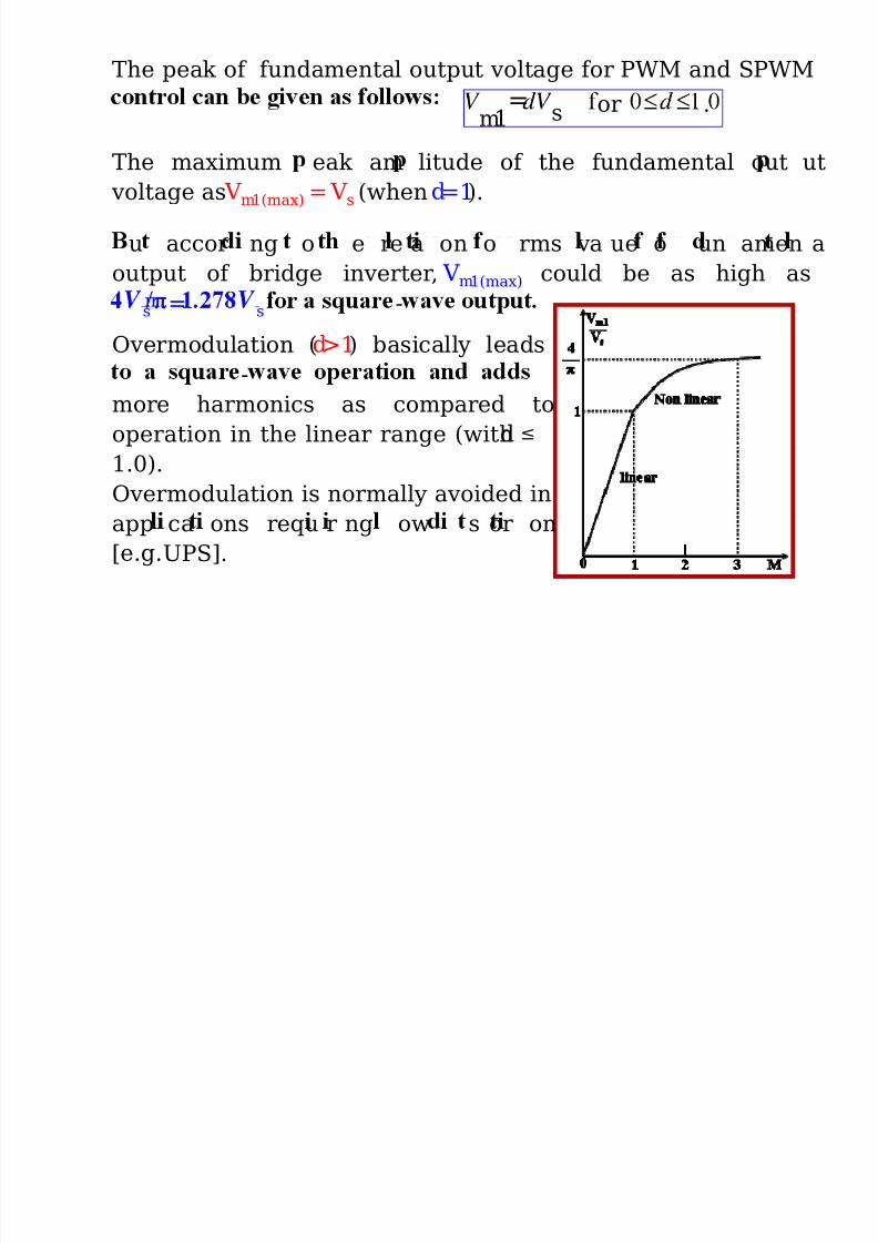
The peak of fundamental output voltage for PWM and SPWM
The maximum eak am litude of the fundamental out ut
.or 1=
sm
voltage as V m1(max) = V s (when d =1).
u accor ng o e re a on o rms va ue o un amen a
output of bridge inverter, V m1(max) could be as high as
π= - s π s
Overmodulation ( d >1) basically leads
-
more harmonics as compared to
operation in the linear range (with d ≤1.0).
Overmodulation is normally avoided in
app ca ons requ r ng ow s or on
[e.g. UPS].
8/12/2019 02 PWM Inverters Part II
http://slidepdf.com/reader/full/02-pwm-inverters-part-ii 24/35
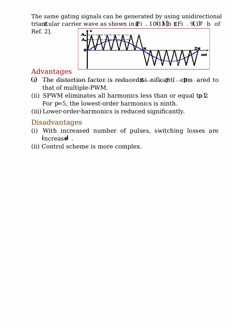
The same gating signals can be generated by using unidirectional
trian ular carrier wave as shown in Fi . 10-15 b Fi . 9.17 b of
Ref. 2].
Advantagesi The distortion factor is reduced si nificantl com ared to
that of multiple-PWM.(ii) SPWM eliminates all harmonics less than or equal to 2 p-1.
For p=5, the lowest-order harmonics is ninth.
(iii) Lower-order-harmonics is reduced significantly.
Disadvantages(i) With increased number of pulses, switching losses are
ncrease .
(ii) Control scheme is more complex.

8/12/2019 02 PWM Inverters Part II
http://slidepdf.com/reader/full/02-pwm-inverters-part-ii 25/35
Modified Sinusoidal Pulse-Width-Modulation (MSPWM)
n ec n que, e w o pu ses a are nearer e peaof the sine wave do not change significantly with the variation of
modulation index.
Thus, the SPWM technique can be modified so that the carrier
wave is applied during the first and last 60o
intervals per half-cyc e e.g. o to o an o to o . s type o mo u at on n
known as MSPWM and shown in Fig, 10-18.
half-cycle is found from:
36/ +=
The fundamental component is
characteristics are improved. It
reduces the number of
switching of power devices and
also reduces switching losses.

8/12/2019 02 PWM Inverters Part II
http://slidepdf.com/reader/full/02-pwm-inverters-part-ii 26/35
Phase-Displacement Control
Voltage control can be obtained by using multiple inverters
an summ ng e ou pu vo ages o n v ua nver ers.
A single-phase full-bridge inverter can be perceived as the sum
- .

8/12/2019 02 PWM Inverters Part II
http://slidepdf.com/reader/full/02-pwm-inverters-part-ii 27/35
A 180o phase displacement produces an output voltages as
-
angle of produces an output as shown in Fig. 10-20(e).
The rms output voltage:π β
sV oV =
Fig. 10-20

8/12/2019 02 PWM Inverters Part II
http://slidepdf.com/reader/full/02-pwm-inverters-part-ii 28/35
The instantaneous voltages equation can be expressed as
∑== ,..5,3,1sin
nt nn saov ω π ∑= −= ,..5,3,1
)(sinn
t nn sbov β ω π
∑∞
=−−=−= ⎥
⎦
⎤⎢⎣
⎡
,..5,3,1
)(sinsin2
n
t nt nnVs
bovaov
abv β ω ω
π
∑∞
=−=
⎥⎥⎥
⎦
⎤
⎢⎢⎢
⎣
⎡
,..5,3,1)
2(cos
2sin4
nt nn
nVs
abv β ω β
π
The rms value of the fundamental output
volta e is: sin4
1nVsV =
The above equation indicates that the output voltage can bevaried by varying the delay angle .
This type of control is especially useful for high-power
app ca ons, requ r ng a arge num er o rans s ors n
parallel.

8/12/2019 02 PWM Inverters Part II
http://slidepdf.com/reader/full/02-pwm-inverters-part-ii 29/35
Advanced Modulation Techni ues
e w c s mos common y use , su ers
from drawbacks (e.g. low fundamental outputvo age .
The other techniques that offer improved
per ormances are:
• Trapezoidal modulation,
• a rcase mo u a on,
• Stepped modulation,
• armon c n ec on mo u a on, an
• Delta modulation

8/12/2019 02 PWM Inverters Part II
http://slidepdf.com/reader/full/02-pwm-inverters-part-ii 30/35
Delta ModulationIn delta modulation trian le wave is allowed to oscillate within a
defined window V above and below the reference sine wave v r.
The inverter switching function, which is identical to the output
vo age v o s genera e rom e ver ces o e r angu ar wave v c as
shown in Fig. 10-27. It is also known as hysteresis modulation.
If the frequency of the modulating wave is changed keeping the slope of thetriangle wave constant, the number of pulses and pulses widths of the
modulated wave would change.
e un amenta output
voltage can be up to V s and
is de endent on the eak
amplitude A r and frequency
f r
of the reference voltage.
e e a mo u a on can
control the ratio of voltage
to fre uenc v/f control ,
which is a desired feature in
ac motor control.

8/12/2019 02 PWM Inverters Part II
http://slidepdf.com/reader/full/02-pwm-inverters-part-ii 31/35
Harmonic Reductions-
inverters can be eliminated by introducing a pair of
symmetrically placed bipolar voltage notches as shown in Fig.
10.28.
The Fourier series of output voltage can be expressed as)46.10(
,..5,3,1sin)( ∑
==n
t nn Bt ov ω

8/12/2019 02 PWM Inverters Part II
http://slidepdf.com/reader/full/02-pwm-inverters-part-ii 32/35
1 2/ )(sin2 )(sin)(sin
4t td nt td nt td nsV
n B α π α ω ω α
α ω ω ω ω π ∫ ∫+∫−= ⎥⎥⎤
⎢⎢⎡
)47.10(2cos2
1cos214
n
nnsV
n Bα α
π
+−=
⎦⎣
Eq. (10.47) can be extended to m notches per quarter-wave, thenthe expression of n becomes:
4 ⎤⎡⎛ V
...
4
cos
3
cos
2
cos
1
cos⎥
⎥
⎦⎢
⎢
⎣
⎟
⎠
⎜
⎝
−−−=π
nnnn
nn

8/12/2019 02 PWM Inverters Part II
http://slidepdf.com/reader/full/02-pwm-inverters-part-ii 33/35
The third and fifth harmonics would be eliminated if B = B =0
and Eq. (10.47) gives the necessary equations to be solved.
⎟⎟
⎠
⎞
⎜⎜
⎝
⎛ −−==+− 5.01
3cos1cos31
2or 0
23cos2
13cos21 α α α α
⎟
⎟
⎠
⎞
⎜
⎜
⎝
⎛
−−
==+− 5.025cos1
cos31
1or 025cos215cos21 α α α α
ese equat ons can e so ve terat ve y y n t a y assum ng
1 = 0 and repeating the calculation for 1 and 2. The result is
= o = o
2 . , 2 . .
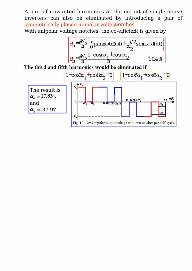
A pair of unwanted harmonics at the output of single phase
8/12/2019 02 PWM Inverters Part II
http://slidepdf.com/reader/full/02-pwm-inverters-part-ii 34/35
A pair of unwanted harmonics at the output of single-phase
inverters can also be eliminated by introducing a pair of
symmetrically placed unipolar voltage notches.With unipolar voltage notches, the co-efficient B n is given by
1
0
2/
2
)(sin)(sin4
t td nt td nsV n B α π
α ω ω ω ω π ∫ ∫+=⎥⎥⎥
⎦
⎤
⎢⎢⎢
⎣
⎡
)49.10(2cos
1cos14
n
nnsV
n Bα α
π
+−=
02
3cos1
3cos1 =+− α α 02
5cos1
5cos1 =+− α α
The result is
= o
and
2 = 37.97o.

8/12/2019 02 PWM Inverters Part II
http://slidepdf.com/reader/full/02-pwm-inverters-part-ii 35/35
The modified sinusoidal PWM techniques can be applied to
effectively in the output voltage as shown in Fig. 10-30.