PSI RFI - CERN Document Servercds.cern.ch/record/1266564/files/PS-RF-Note-94-21.pdf · european...
16
EUROPEAN ORGANIZATION FOR NUCLEAR RESEARCH ORGANISATION EUROPEENNE POUR LA RECHERCHE NUCLEAIRE CERN - PS DIVISION PSI RFI Note 94-21 DESCRIPTION OF "INDUCTANCE BIAS CONTROL" (PSIRF-LL 2034/2) AND "INDUCTANCE BIAS CONTROL INTERLOCK" CARD. B.J. Evans Geneva, Switzerland 29 April, 1994
Transcript of PSI RFI - CERN Document Servercds.cern.ch/record/1266564/files/PS-RF-Note-94-21.pdf · european...
EUROPEAN ORGANIZATION FOR NUCLEAR RESEARCH ORGANISATION EUROPEENNE POUR LA RECHERCHE NUCLEAIRE
CERN - PS DIVISION
PSI RFI Note 94-21
DESCRIPTION OF "INDUCTANCE BIAS CONTROL"
(PSIRF-LL 2034/2) AND "INDUCTANCE BIAS CONTROL
INTERLOCK" CARD.
B.J. Evans
Geneva, Switzerland 29 April, 1994

1 GENERAL DESCRIPTION
Waroin&
There are at least three errors on the "Inductance Bias Control" drawing (PS/RF-LL
2034). On the PCB :-
• Pin 14 IC2 goes to IC's 19,21 pin 1.
• Pin 15 IC2 goes to IC's 19,21 pin 19.
• BR2 is connected to SWI pin 5.
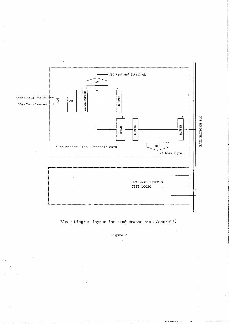
The "Inductance Bias Control" is used as part of the "fast feedback" system installed on
the 9.5 MHz ferrite cavities.
The circuit is shown in Fig. 1 (a block-diagram is shown in Fig. 2). The resonant
frequency of the main accelerating cavities of the PS is given by the bias current in their
ferrites. This is digitized (individually for each cavity) by an "Inductance Bias Control" at a
sample rate of approximately 50 kHz. The sample pulse may be either from IC2 or external to
the card. In the latter case, IC3 is switched to pass a signal from SKI, pin 15b.
The digitized signal goes to a pair of EPROMs, (ICI6 and ICI7, Fig. 1). These have
been specifically programmed for each different amplifier plug-in of the PS to maximize
closed-loop stability of the fast feedback (IC31 output drives a voltage-controlled current
source that biases and tunes a resonant circuit in the grid of the fmal amplifier).
There are two interlock functions implemented on the card. The ADC output is
immediately sent to a DAC which reconstitutes the analogue input. This output is compared
to the "Sample and Hold" input where an error is signalled if the difference is too large (IC28
pin 11).
The driving bias-current is also monitored by the card. This is compared with the
requested current and again an error is signalled if the difference is too great (IC28 pin 3).
The sum of the two errors is sent on the backplane to the "L Bias Control Interlock" card (see
below). The error signal may be blocked by BR2 or by SWI.
2 DESCRIPTION OF PLD IC4
Different test possibilities have been included on the "Inductance Bias Control" card.
These would normally need the use of a test-card also connected to the backplane.The
different functions (described below) are selected using the front-panel switches SWI and
SW2. These are :
1

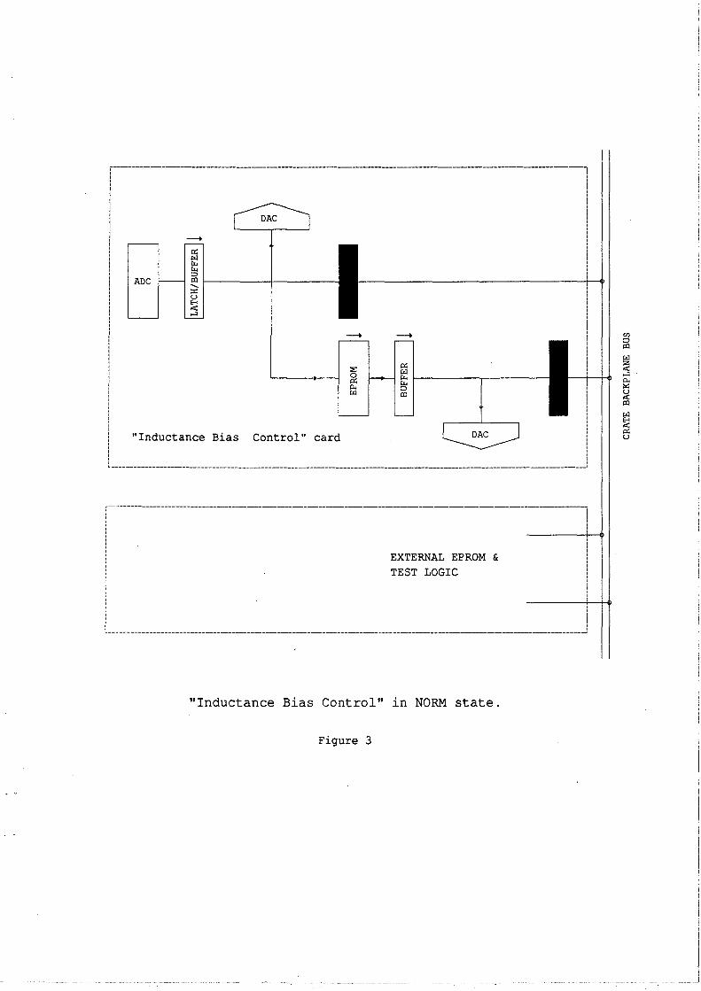
i) SWI "Nonn(al)", SW2 "don't care" (Fig. 3).
In this state, no data is either sent or received from the backplane.
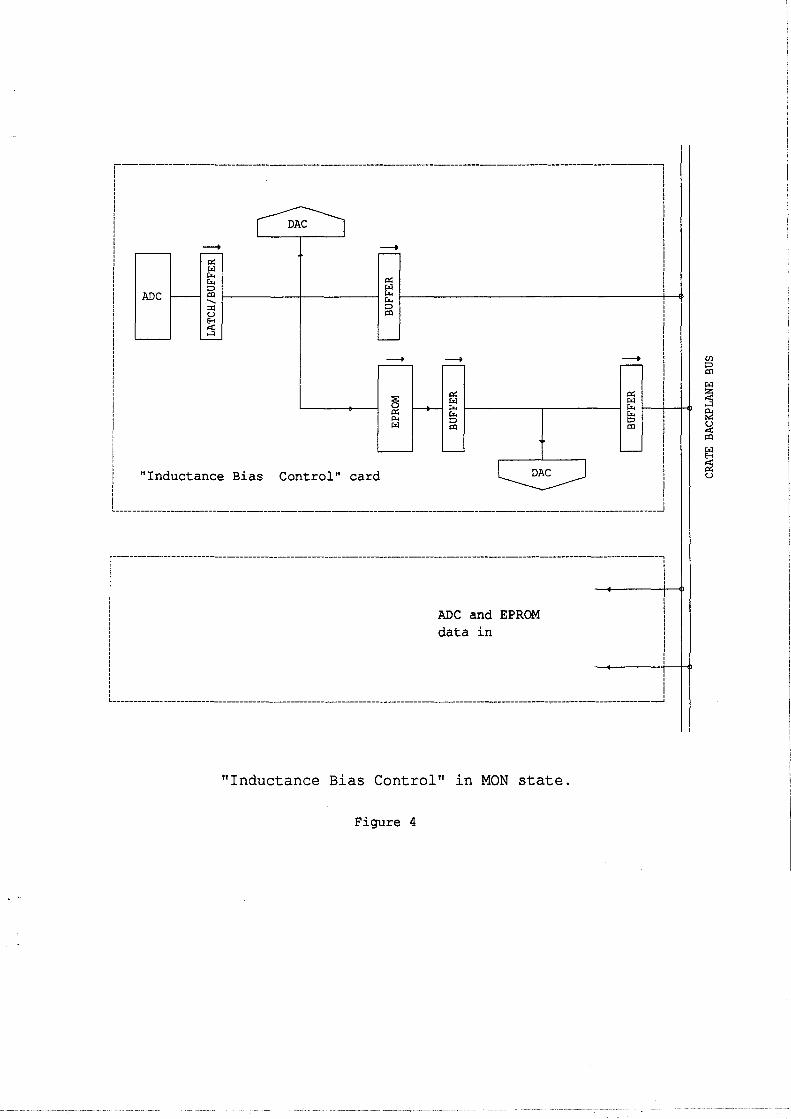
ii) SWI "Mon(itor)", SW2 "don't care" (Fig. 4).
In this state, both the ADC and EPROM data are sent to the test card.
iii) SWI "Test", SW2 "ADC-X-DAC" (Fig. 5).
The ADC data could be sent to an external EPROM which returns programmed data.
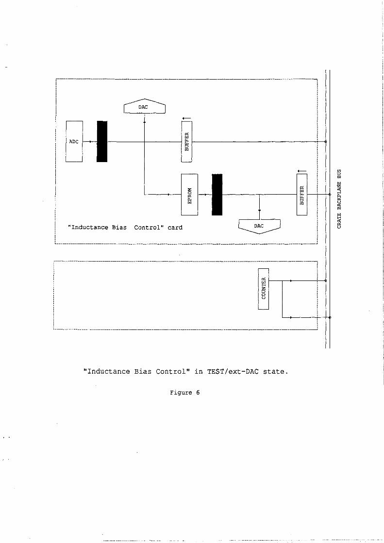
iv) SWI "Test", SW2 "ext-DAC" (Fig. 6).
Both DACs may be tested using an external counter.
v) SWI "Test", SW2 "ROM2 (Fig. 7).
The EPROM data may be read directly from the test-card.
NOTE: For cases ii), iii) and v) above, only one card may be active at any time.
The PLD ABEL file is given in Appendix 1 and is stocked in the engineering" PC
under C:\P ALS\LBIAS\LBIASIC4.ABL.
3 "LBIAS CONTROL INTERLOCK" (Figs. 8-12)
This looks for three possible faults.
i) The interlock bit from each cavity (described above).
ii) The "Inductance Bias Control" crate power-supplies.
iii) The + 24V supplies for the LEM's used to monitor the four coarse-tuning currents.
Note that this card must be plugged into the far right-hand slot of the crate.
Distribution:
R. Garoby D. Grier P. Konrad G.Lobeau P. Maesen F. Pedersen J-P. Terrier J. Vallet
2
'Coarse Tuning' current
"Fine Tuning" current
r r r r i r r r r r r r r r r r
---+
~ r<I Ii< Ii< => j:Q ...... ::c u E-< ..: ...:I
"Inductance Bias
ADC test and interlock
+--+
~ r<I Ii< Ii< => j:Q
---+ ---+ +--+
Control" card
i L bias signal l _________________________________________________________________________________________ _
r-----------------------------------------------------------------------------------------'1
EXTERNAL EPROM & TEST LOGIC
r r r r r
r i r r
... _--------------------------------------------------------------------------------------------------'
Block Diagram layout for "Inductance Bias Control""
Figure 2
I I
ADC
"Inductance Bias Control" card
0: ~
~ r---------.----------o r:o
EXTERNAL EPROM & TEST LOGIC
"Inductance Bias Control" in NORM state.
Figure 3
:--------------------------------------------------------------1 , , : I , r
I I , r
I I
r r
ADC
p: ~ r.. r.. => co ...... ::t: U ~ rot ....:I
p: ~ r.. r.. => co
--+ --+ --+
: ! ::0:
0 ~ ~
r r.. r.. : p: r.. r.. 1 0..::>:::> I Pa:J Ql r::a , ! r , ! ! "Inductance Bias Control" card I :
r
i I
L _____________________________________________________________________________________________________ -.J
r----------------------------------------------------------------------------------------------------------1 ! I ! I , : , t ADC and EPROM ! data in ! , I r I : L ___________________________________________________________________________________________________________________ J
"Inductance Bias Control" in MON state.
Figure 4
r r

-+ -+
0:: ~ t>..
0:: t>.. :::> ~
ADC III t>.. ...... t>.. ::c :::> u III Eo< o<C ....:I
+-- Ul :::> III
~
0:: Z :;: ~ o<C
~ t>.. ....:I t>.. ~ p., :::>
~ III ~ III
~ Eo< o<C 0:: U "Inductance Bias Control" card
"Inductance Bias Control" in TEST/ADC-X-DAC state.
Figure 5
,---------------------------------------------------------. I I I
I I I I I I I I
I I
I I I I I
I I I 1
! I
I I
I I I
I I I I
1 I
I I
I I I
I i I
ADC
"Inductance Bias Control" card
t:>: r.:I Eo< Z o o u
"Inductance Bias Control" in TEST/ext-DAC state.
Figure 6
f--
t:>: r.:I ~ ~ 0 ~
CJ) 0 ~
r.:I Z oet: ...:1 0.. :.:: u oet: ~
r.:I Eo< oet: t:>: u

ADC
p:; <zl
-----------+--------~ ~ r-------------------------------------+_~ I:) co
--+ --+
::;:: p:; p:; <zl <zl
0 t.. t.. p:; t.. t..
"" I:) I:) <zl co co
"Inductance Bias Control" card
~ r-----~------~~ E-< z I:) o u
EPROM data in
"Inductance Bias Control" in TEST/ROM state.
Figure 7
CI) I:) co <zl
j "" :.:: ~ co <zl E-<
~ U

INDUCTANCE BIAS CONTROL BACKPLANE (upPER CONNECTOR)
ROW A ROWB
1 GND GND 2 BUS 1 DO BUS 1 Dl 3 D2 D3 4 D4 D5 5 D6 D7 6 D8 D9 7 DIO D11 8 BUS 2 DO BUS 2 Dl 9 D2 D3 10 D4 D5 11 D6 D7 12 D8 D9 13 DIO D11 14 GND GND 15 End of conversion (+5 V = True) Test Card Clock 16 MPX Selector Input 17 GND GND 18 Fault Cavity 51 Fault Cavity 36 19 " 56 " 46 20 " 66 " 86 21 " 76 " 96 22 " 81 " 11 23 " 91 " Test 24 25 26 27 28 Fault Out 29 30 31 I +5V Digital I +5V Digital 32 GND GND
FIQURE9.

INDUCTANCE BIAS CONTROL BACKPLANE (LOWER CONNECTOR)
1 2 3 4 5 6 7 8 9 10 11 12 13 14 15 16 17 18 19 20 21 22 23 24 25 26 27 28 29 30 31 32
ROW A
Ground
Fault Cavity 51 " 56
-15V
" 66 " 76 " 81 " 91
36 46 86 96 11 Test
Lem+24VCfl Lem+24VCf2 Lem+24V Cf3 Lem+24VCf4
+15V " Bridge
I +5V Analogue Ground
ROWB
Ground
-15V
+15V
I +5V Analogue Ground
FIGURE 10.

(AVI TIES II lOCI<.
CII
. G> 51
0 S"b
0 "h <:> T6
o 81
0 91
c'T4
o (( 0 /ES1
Ftl>NT P AfJT2.L fo~
CA\lIIIES :r. 'LOCK
- . FIGURE 11.

~
~ 0
C'\I
~ ...-l
~ p:;
<3 ;:J ~ H IZ-<
V\ ~
~
N ~ "'(- ~ ®® \-
®{) @)(f) () ! "> ~~
®® 1:j1- ~
~
I I. I ...l) .,J)
~ .$1 ~
""" "<lit ~ - t!.I L , 0 0 @ a 0 0 ~
I..,)
0 0 0 0 0 0 :1 ~ ~ ~ ~
In ~ -..J). rT ~ <3' ~ L ..J

L ,
APPENDIX 1 Listing ofp.l.d. ABEL fIle "C:\PALS\LBIAS\LBIASIC4.ABL"
module Ibias flag '-r3' title' pld for L bias control John 18/03/94' "PLEASE NOTE!!! "This is a copy of the pal in the L bias control. "It does not simulate exactly like the installed IC. "(This has been re-written for dsy-srv3. The original "programme was on the PC in the CO group). "The differences should be unimportant as they concern "the direction pins of the buffers when they are in the tri-state "position.
ic41bias device 'pl0l8'
"Inputs SIp2 pin 1 SIp5 pin 2 S2p2 pin 3 S2p5 pin 4
"Outputs E8 pin 19 ; E18 pin 18 ; E9 pin 17 ; D9 pin 16 ; EI9 pin 15 ; DI9 pin 14 ; H,L,X,z,C,P = I,O,.X.,.Z.,.C.,.P.;
Equations !E8 = SIp5 # !S2p2; lEI8= SIp5 # (S2p2 & S2p5); E9 = SIp2 & SIp5; D9 = SIp5 # !S2p2; !EI9= !SIp2 # !SIp5; DI9 = SIp5 # (S2p2 & S2p5);
tese vectors ([SIp2,SIp5,S2p2,S2p5]->[E8,EI8,E9,D9,EI9,DI9]) [0 ,1 , ° ,1 ]->[ 0, 0,0,1, 0,1 ];"mon [0 , 1 , 1 , ° ]->[ 0, ° , 0, 1, 0,1 ]; [0 , 1 , 1 , 1 ]->[ 0, ° , 0, 1, ° , 1 ];
[1 , ° , ° , 1 ]->[ 0, 1 ,0, 1, ° , ° ];"test ADC-X-DAC [1,0,1,0 ]->[I,I,O,O,O,O];"testEXT-DAC [1,0,1,1 ]->[I,O,O,O,O,I];"testROM
[1 ,1 , ° , I ]->[ 0, 0,1, X, 1 , X ];"norm [1 , 1 , 1 , ° ]->[ 0, ° , 1, X, 1 , X ]; [1 , 1 , 1 , 1 ]->[ 0, ° , 1, X, 1 , X ];
end Ibias

WIn fM.:'1 SI At( --~
Sb 1\6 I I - ~
_(,_, ~lO I I " ~
"*' ,\2.\ - ' I :;'~I~-i
$1 422..- I I -~
C31 ~2$. I , ~ ,
3" 'Ii I. U "
4b .,' d I I III
1''' J2D.J I I ;(.~
5&' &L\ «I " t~ -l
" &22. • :., I I ..~ {olt-
bT JZ3 I I II I ;~~ ~ Co '" Nft.:r£,(r1
S/APU.tEIA(t
220.Q,·
// LDiAG~
·AI
.J
J
¥
Ics
1-3 ~HC1oZ
4- 1-411(. ,00
S U'/3Z4-, 1~L5Z.1
iJ.ltj "qS4"2.. ((J"f 4)
ql *- (ScIO-;r
IZ1o.ll LfM~ ;./ j/o~~ @ ...- f*i" r PttrJ~L ~ ~ i
--~ ___ u _____ - ___ .~ ......... --.-....
J~ "'4 2&'<L~ i -
(+ISY) l,oa. -\ sJ IHf.t('t\&.-
to9.1l. Psu Ot(
J j.l" Iii" ;!t1fJ:
II
IS~ .... LeM t2AN C,T I ~ J 2.1~·3 ~
IbCl C.TZ - ~ I~ C.1"3
:~~~ C1i \ &
SA\-1.P >\aJ? ~o
.~
1Ao
-- --FIGURE 8.
L BiAS CotJl((O L. 'tJ~C?:LDGK c.AI'D.

~'" ,,,
K2 CONNECTOR I
,.... :" :~ 70b :;iJ' :"., l"" ;: . ,---6-, 32b~:,,,,,~,,, ,CO 320 , n.,
f.TIN (FP)
Lr IN (F.P)
(f-.PI
Tll~T~ t ~i' ;:~ ::J _lSV
1" J 2 ")SK9 1
I 1" I ~)SK10' ,~ 1
1
"" 5.1K U ,,-.,-y",
~.~~K i },Gop! •. .!-::, , =--r-;; I'"''
)~ ~-
co
CONNECTOR I ~:~~.1SV I I~;t' I Ii~~f
! I,
TEST~ ~ 3'" "'
'" .,
armOR $c:''--''-+'j,'-___ ,
'" '" 1'19
m r-.=t2K
~AQI~
" r-;;-
1(7
, I"
co ",
." 10'
'" 10
1(15
"" "
.co I" --=-
6\18
S2 'l
'" ...
r--iF-
'" '"
R\e.1K
'" 10
hH
"" "
." '1>
'" 1.~SK
1~ 1110 ""ij"" ." " '
'1 " ~',
r---:~
~
PSKB
~ --"1 _2
-, -I -I
"
AOC TEST
SK4
I H~~~~~:~l'¢ . I ---f"L "" ~~~ C,-' ~ ., : ~' -. -84 ,5 ""-,, :: I
<C"'~~~- '" ., ,." ~- ~., .. EXT l~~~~~~!E~~~" '21~ ~~~
: :: :::: "" Al il 16
; AA 1[19 ~ " 89 , " • " 88 . := ::
'" ., " '"
119
SK1 CONNECTOR S
" n,
I
21 Al0
'" --"'Ae '"
.£;'~' " " 03 ,3
O~ 15 l§'''',Ji
4 M 1(17
118
lleH lsot.t,on
D,~~,' ~ : OA:A;o ~ a,us
[~:1~~~~~HtaE~~~~' )"--.t;,.. 129 3 A! 92 1J 12b
ICZQ ::!![21~~: ~~~
IN PERTURBATION
~, r-----S>---------+---i;y~ IF,P)
SK7 .PI IIII III' II In I
m r-----"
1(111l~
15u L---....J
[(27
~~.~=-oJ IOl I(:r"V"YV' Ie .tU1 T~!?,F Tn,lr' ;~l"F ;22"f
TO AU SV SUPPLIES EXCEPT£D ADCAMDDAC
RESI,TOR,
RlJ,14,39,40, R41i R4',49,5Q,5I.,'>S
B 1
1(4.8.9,11,18,20 I lC21
}- AB 1II.W.$%
t
CAPA(ITORS
[;1,12,0,'<[41
n EJ
B 1(16,17
Typo WIM}\ FKSl POlYESI!R
0,1 ~f
CD lootai pe.l. 1 pF J ~5V
1(;,11,13,,1,,22,14,15,30
?OTENTIO~En~, :~ooao;;\~
.,.;
>''+---<''-<r;) OUT
SK6
'----l'--A ~EUiT SK5
I DATE PS/RF_LL 2034 (J14022) 2/{l2($1-
INDUCTANCE BIAS CONTROL
_~""ii:,1ii!~.]l£':""~ IPS/RF.LL 2034/2-1 liT
"