processing - University of Torontojohns/ece334/lecture_notes/processing.pdf · University of...
17
slide 1 of 17 University of Toronto Processing
Transcript of processing - University of Torontojohns/ece334/lecture_notes/processing.pdf · University of...

slide 1 of 17University of Toronto
Processing

slide 2 of 17University of Toronto
Silicon Wafer • Create 8-12 inch diameter cylinder (1m long) of
single-crystaline silicon with light doping (usually p-) • Ingot cut into wafers about 1mm thick
Photolithography
• Portions of silicon wafer are masked out so processing can be applied to remaining areas
• First create glass mask with dark areas using e-beam(cost of mask set $25k-$1M)
• Thermally grow SiO2 on wafer, apply negative photoresist, align glass mask and expose to UV light
• Photoresist hardens (after baking) where exposed to light, remaining region removed (including SiO2)
• Negative since SiO2 remains where mask is light

slide 3 of 17University of Toronto
Photolithography
Opaque
Ultraviolet light
Translucent
Hardened photoresist, PR1
Glass
SiO2
p– substrate
mask
region region
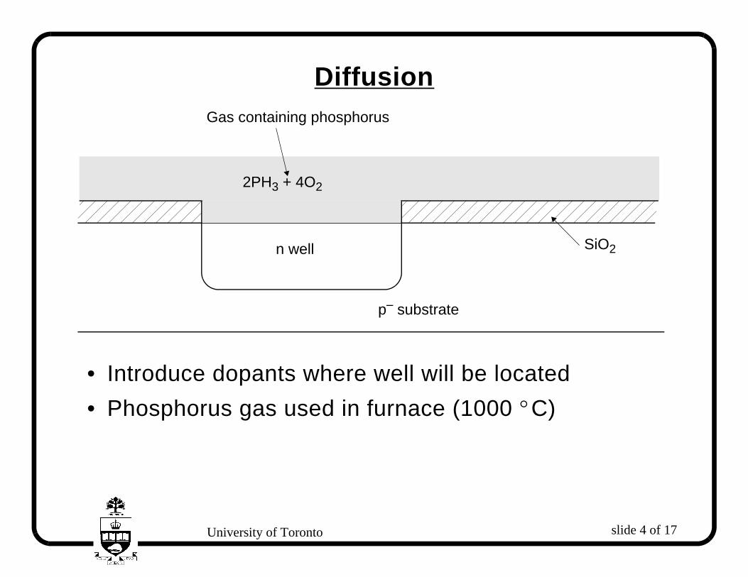
slide 4 of 17University of Toronto
Diffusion
• Introduce dopants where well will be located
• Phosphorus gas used in furnace (1000 C)
2PH3 + 4O2
p– substrate
SiO2n well
Gas containing phosphorus
°
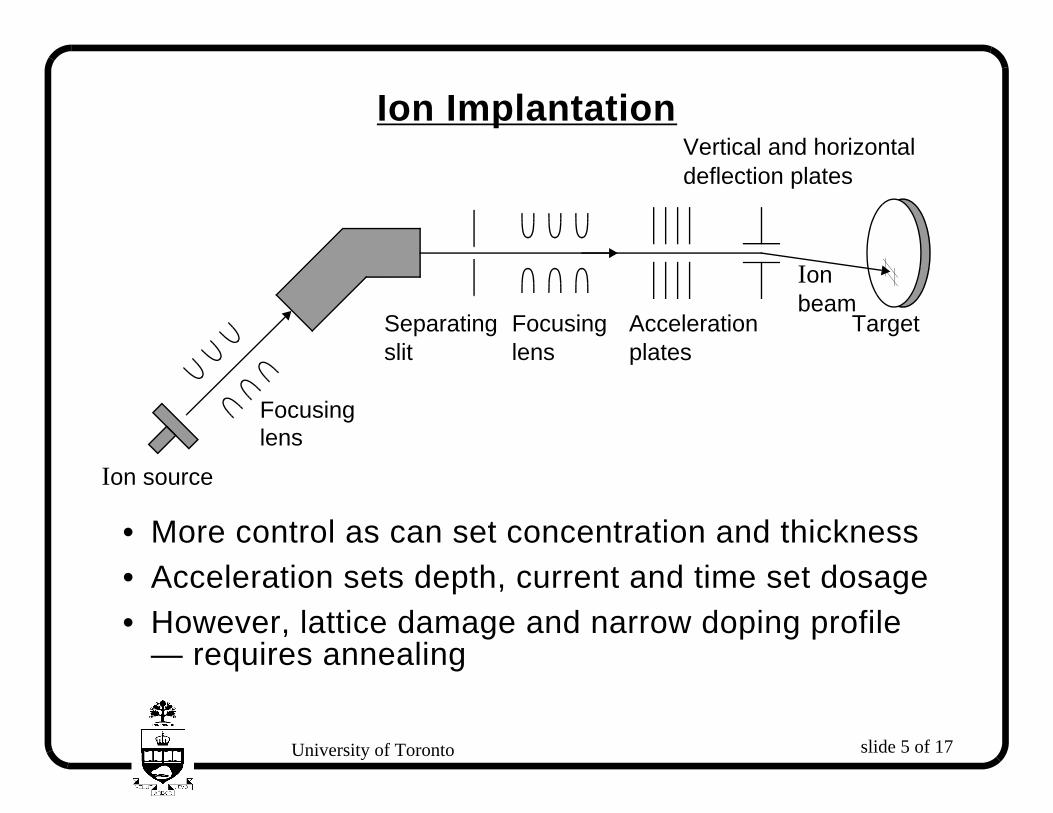
slide 5 of 17University of Toronto
Ion Implantation
• More control as can set concentration and thickness • Acceleration sets depth, current and time set dosage • However, lattice damage and narrow doping profile
— requires annealing
Ion source
Focusing
FocusingSeparating Acceleration
Vertical and horizontal
Target
Ion
deflection plates
beam
slit lens plates
lens
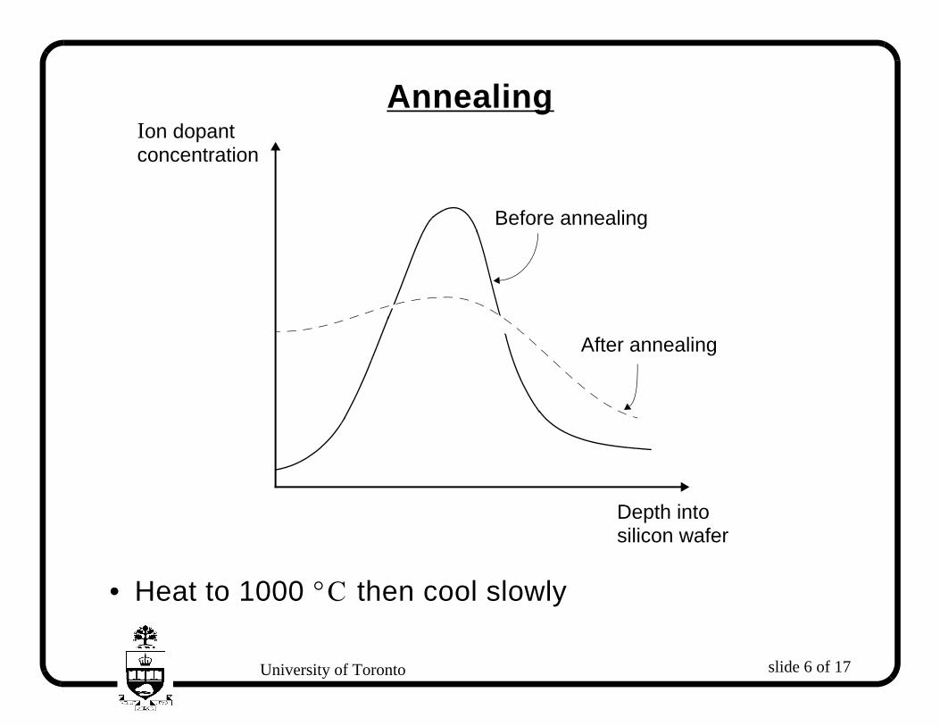
slide 6 of 17University of Toronto
Annealing
• Heat to 1000 then cool slowly
Ion dopant
Depth into
Before annealing
After annealing
concentration
silicon wafer
°C
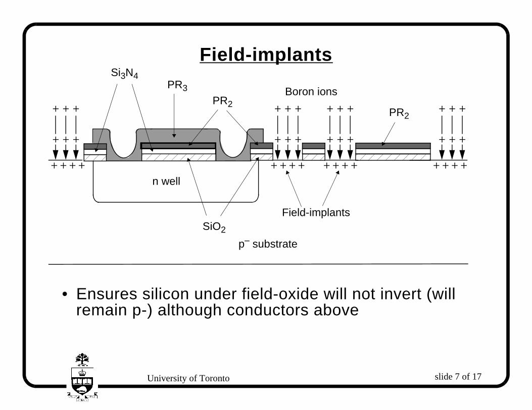
slide 7 of 17University of Toronto
Field-implants
• Ensures silicon under field-oxide will not invert (will remain p-) although conductors above
n well
SiO2
p– substrate
Si3N4PR3
PR2PR2
Field-implants
Boron ions
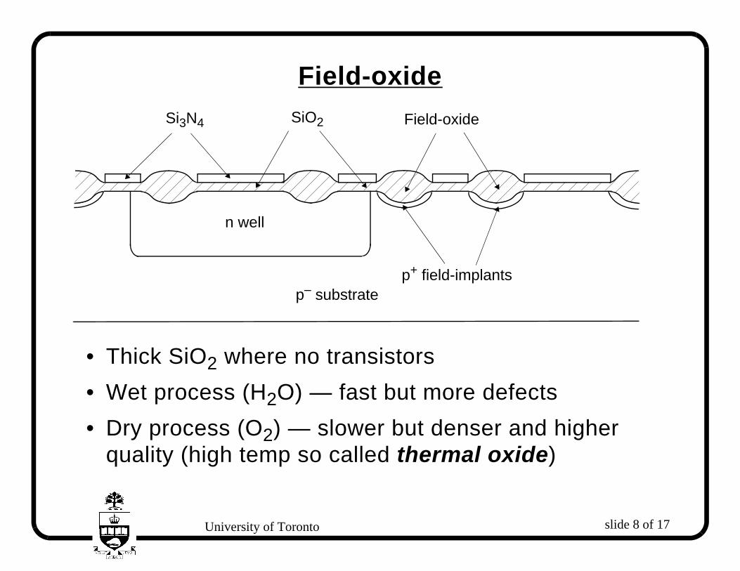
slide 8 of 17University of Toronto
Field-oxide
• Thick SiO2 where no transistors
• Wet process (H2O) — fast but more defects
• Dry process (O2) — slower but denser and higher quality (high temp so called thermal oxide)
Si3N4 SiO2 Field-oxide
p+ field-implants
n well
p– substrate

slide 9 of 17University of Toronto
Thin gate-oxide and threshold-adjust
• Thin oxide grown using dry process (0.01 ) • If n-well more heavily doped then single boron
implant will adjust Vtn from -0.1V to 0.8V and Vtp from -1.6V to -0.8V
Thin gate SiO2 Field-oxide
p+ field-implants
n well
p– substrate
Gate threshold-voltage-adjustimplant
µm
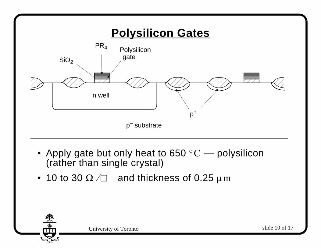
slide 10 of 17University of Toronto
Polysilicon Gates
• Apply gate but only heat to 650 — polysilicon (rather than single crystal)
• 10 to 30 and thickness of 0.25
p+
n well
p– substrate
SiO2
PR4 Polysilicon gate
°C
Ω ⁄ µm
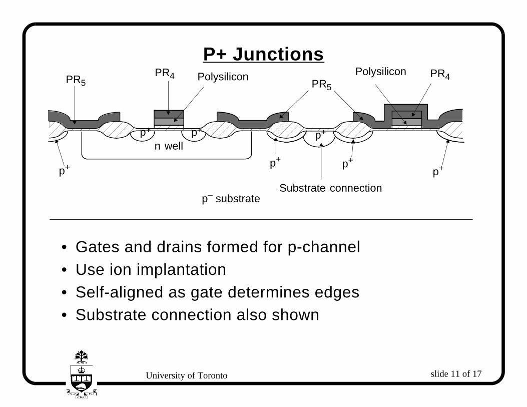
slide 11 of 17University of Toronto
P+ Junctions
• Gates and drains formed for p-channel • Use ion implantation • Self-aligned as gate determines edges • Substrate connection also shown
p+
Substrate connection
n well
p– substrate
p+p+ p+p+
PR5PR4 Polysilicon
PR5
Polysilicon PR4
p+ p+

slide 12 of 17University of Toronto
N+ Junctions
• p+ regions protected and n+ implanted • Requires annealing after since ion implantation used • Would melt gate if it were metal
p+
Substrate tie
n
p–substrate
p+ p+p+
Polysilicon gates
n+ p+p+ n+ n+n+
n-channeljunctions
PR6 PR6
Well tiep-channeljunctions
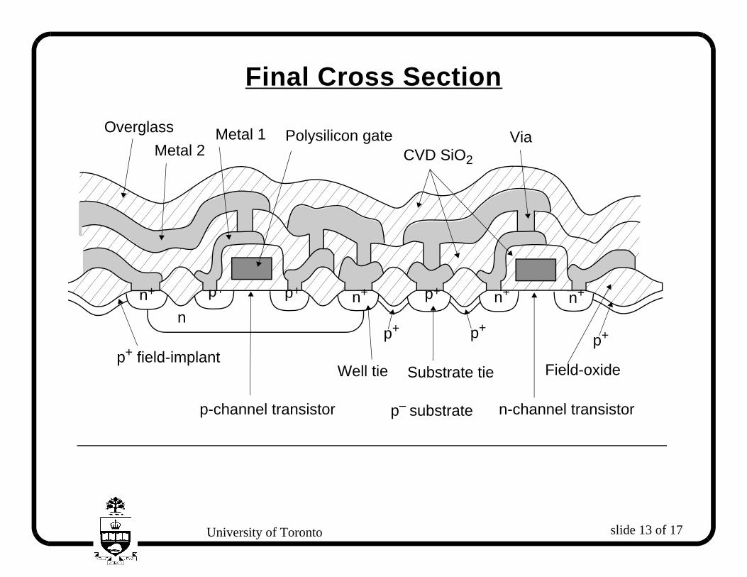
slide 13 of 17University of Toronto
Final Cross Section
Overglass
Metal 2Metal 1 Polysilicon gate
p+
CVD SiO2
p+ field-implant
p-channel transistor
Well tie
p– substrate n-channel transistor
Substrate tie
p+
Field-oxide
Via
p+ n+p+n+ n+n+p+
p+n
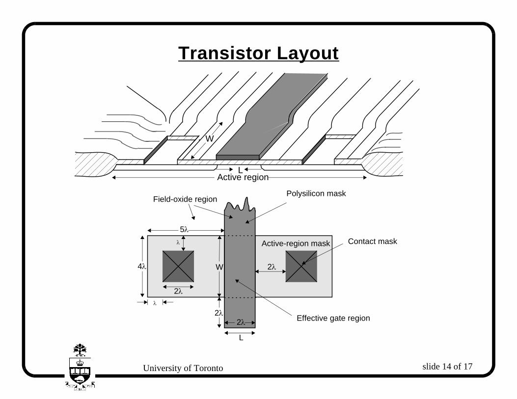
slide 14 of 17University of Toronto
Transistor Layout
W
LActive region
Polysilicon maskField-oxide region
Active-region mask Contact mask
2λ
2λ2λ
λ
2λ
W
Effective gate region
L
λ
4λ
5λ
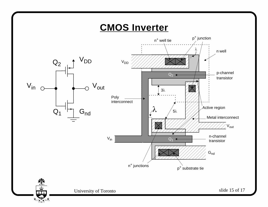
slide 15 of 17University of Toronto
CMOS Inverter
Vin Vout
VDD
Gnd
n+ well tie p+ junction
n well
p-channel transistor
3λ
5λ
Polyinterconnect
λ Metal interconnect
n-channel
n+ junctionsp+ substrate tie
Gnd
Vin
Vout
VDD
λ
Active region
transistor
Q2
Q1
Q1
Q2

slide 16 of 17University of Toronto
Single Large Transistor (4 in parallel)
Metal interconnect
Active region
J1
Gates
Q1 Q2 Q3 Q4
J2 J3 J4 J5
Node 1
Node 2 VG

slide 17 of 17University of Toronto
Schematic of Large Transistor
Node 2 VG
Node 1
Q1 Q2 Q3 Q4
J1 J2
J3
J4 J5
VG
J1 J3
J2 J2
J3
J4 J4
J5
Node 1
Node 2
Q1 Q2 Q3 Q4