Probing Challenges with Cu Pillar - SWTest.org€¦ · Probing Challenges with Cu Pillar Phill Mai,...
24
Probing Challenges with Cu Pillar Phill Mai, JEM America Joe Mai, JEM Europe
Transcript of Probing Challenges with Cu Pillar - SWTest.org€¦ · Probing Challenges with Cu Pillar Phill Mai,...

Probing Challenges with Cu Pillar
Phill Mai, JEM AmericaJoe Mai, JEM Europe

Overview• Crown-tip probe limitations• MEMS probe with flat tip• Summary• Future work
2Mai

Crown-to-bump contact
3Mai
Piercing Contact Probe mark Abrasive/Gel Cleaning
Crown-to-bump CRES stability
4Mai
Cleaning Cycle_TT Sheet
0.0
0.5
1.0
1.5
2.0
2.5
3.0
1 39 77 115
153
191 29 67 105
143
181 19 57 95 133
171 9 47 85 123
161
199 37 75 113
151
189
TD数
抵抗値(Ω
)
Cleaning Frequency
200 TDs
CRES vs TDS
Touchdowns
Test conditions:• Crown tip dia: φ65 μm• Bump: Pb-free, φ90 x 65 μm• Probing OD: 50 μm from last pin• Cleaning OD: 100 μm from avg. pin height• Frequency: every 200 TDs• Number of TDs/clean: 10• Lateral movement: X390 μm, Y390 μm after each TD • CRES of probe only; test cabling subtracted.

Crown-to-Cu pillar contact
5Mai
Slicing Contact Probe mark Abrasive/Gel Cleaning not so effective in the long term

Initial Crown-to-Cu pillar CRES stability
6Mai
・Current: 50mA
*CRES includes about 2 ohms of resistance due to PCB, Space transformer, Interposer, and probe body.
RT (30℃) HT (125℃)
200TDCL10TD
200TD
CL10TD CL10TD200TD
LT (-35℃)
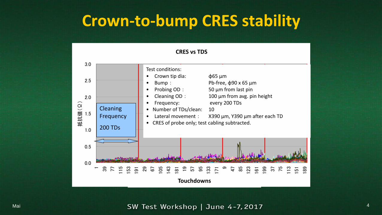
Long term Crown-to-Cu pillar CRES stability
7Mai
Adhesion of SnAgcauses CRES instabilityafter 50K TDs

Crown Tip Contamination with eutectic solder
8Mai
Pb debris remainsBefore laser After laser
Laser: IMT800MVBeam dia.: ~3 mm
In 2007…

Crown Tip Contamination with Pb-free solder
9Mai
REF: “Probe Card Cleaning by Laser”, J.M. Lee et.al., SWTW 2010
Before laser After laser
Laser: IMT400PBeam dia.: ~3 mm
In 2016…
Si peak is from cleaning sheet.
Only probe materials
Only probe materials

MEMS Technology (MT) as an Alternative
10Mai

MT Probe Card Structure
11Mai
Upper guide plate&Upper stiffener plate
Bottom guide plate&Bottom stiffener plateMEMS Probe
PCBStiffener
Interposer(Reflow)
Space transformer

MT Probe
12Mai50μm
55μmBefore lateral slide
After lateral slide
Upper guide plate
Bottom guide plate
MT Probe characteristics
◆ Straight probe allows easy assembly and maintenance
◆ Composite (multi-layer) structure optimizes mechanical and electrical properties, and reduces probe wear.
◆ Tip material: Pd alloy

MT PROBE MECHANICS
13Mai
Initial OD160μm
recommended OD(from last touch)
Limit OD

Guide Plate Selection
14Mai
0
300
600
900
1200
1500
Silicon GuidePlate
Si SiO2 A-484 (Al2O3) SN-240(Si3N4)
[MPa
]Bending Strength
Guide plate A has high bending strength and low friction.
Guide plate A
A B C D E
Guide plate materials
Hardened surface
Hardened surface

Probe Force Hysteresis
15Mai
Initial Guide Plate Optimized Guide Plate
Pro
be fo
rce h
ystere
sisD
iffere
nce
SampleDifference
int 1M
N1 0.65gf 2.28gf
N2 0.57gf 1.72gf
Ave. 0.61gf 2.00gf
SampleDifference
int 1M
N1 0.13gf 0.44gf
N2 0.18gf 0.56gf
Ave. 0.16gf 0.50gf
Difference
Probe : 2.5g Contact force version
Difference
Top
Bottom

Guide-plate Wear
16Mai
View: Top of the Guide Plate Oblique Angle View
Initial Guide Plate
Optimized Guide Plate
Wear :4.4~5.5μm(n=5)
Wear :2.1~3.1μm(n=4)
Top
Bottom

MT-to-Cu Pillar Probe Mark (multiple contacts)
17Mai
Percentage of flat-to-initial diameter 34% 36% 38% 49% 54% 60% 27% 28% 30%
Contact Mark Diameter (μm) 12 13 13 17 19 21 10 10 10
Contact Mark Depression (μm) 0.8 0.9 1.5 2.0 2.5 3.4 0.6 0.6 0.8
Temp.TD counts 1st 2nd 5th 1st 2nd 5th 1st 2nd 5th
ContactMark
30℃ 125℃ -40℃
RT -40℃125℃

Flat-to-Cu pillar CRES Stability
18Mai
*CRes includes ~2 ohms of resistance due to PCB, Space transformer, Interposer, and probe body.
・ Current: 50 mA・ OD: 70μm (from last pin)・ Cleaning Sheet: WA6000 lapping paper・ Cleaning Sheet OD: 70μm (from last pin)
RT (30℃) HT (125℃) LT (-35℃)
CL3TD200TD

Current-Carrying Capacity (CCC)
19Mai
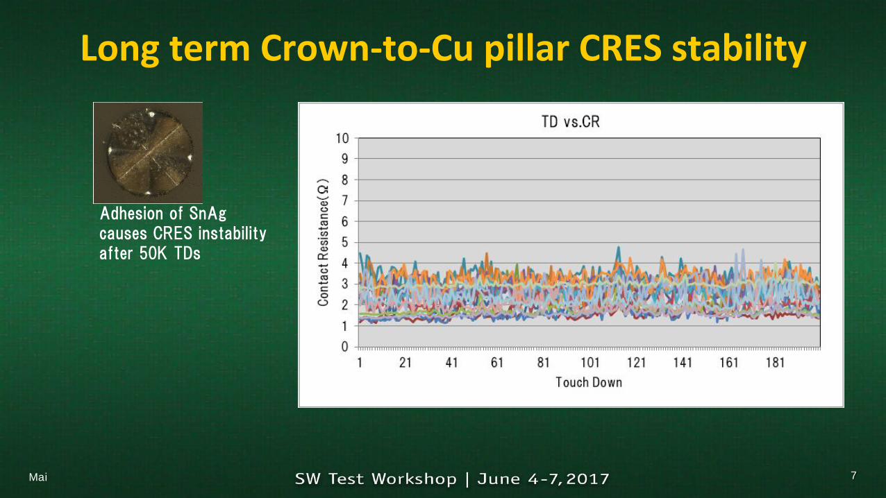
Maximum Allowable Current (MAC)
20Mai
MAC : ~650mA
・ MT probe for 80 um pitch・ Contact OD:MT 70μm / VS 100μm・ Pulse:10Pulses @ 1 min-on/1 sec- off・ Current: 600, 650, 700, 750mA・ Number of Pins: 3 pins for MT and VS

Bandwidth
21Mai
G S_P S_N G
■ Sparameter Model
MT80 - Differential S11 MT80 - Differential S21
-1dB at 20 GHzPitch:80μmLength:7.23mm
< -20dB up to 10GHz
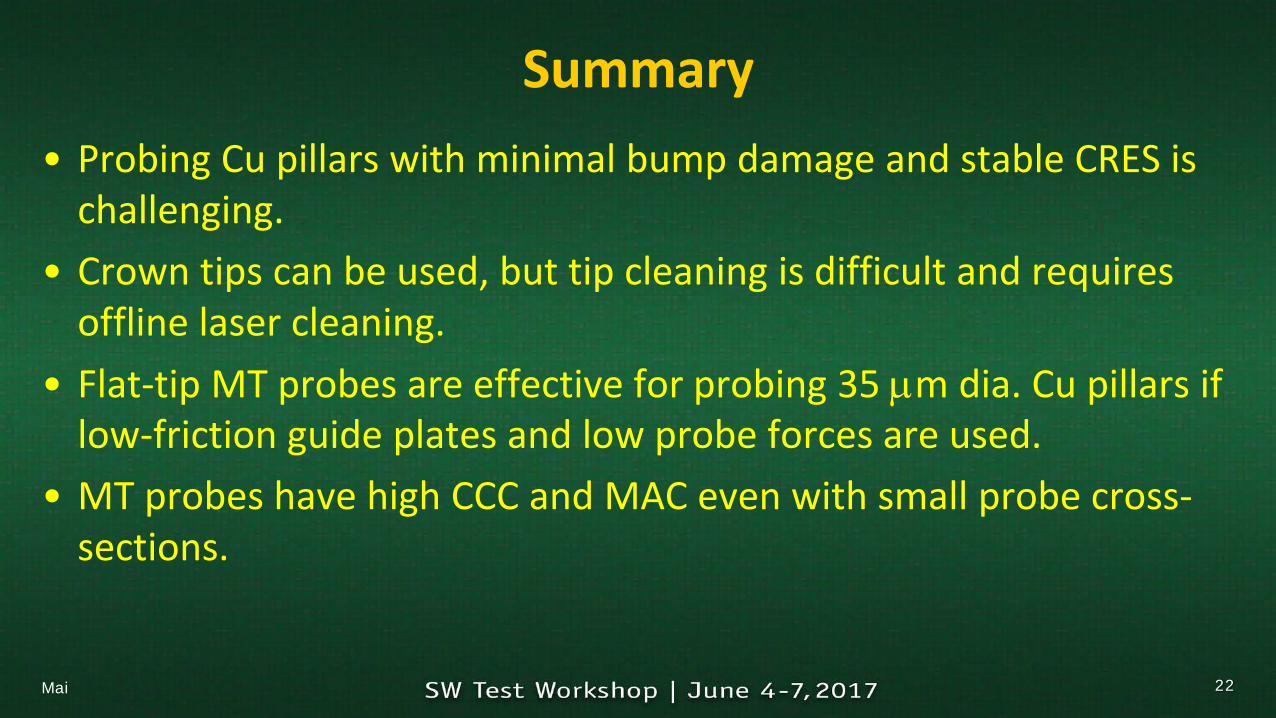
Summary• Probing Cu pillars with minimal bump damage and stable CRES is
challenging.• Crown tips can be used, but tip cleaning is difficult and requires
offline laser cleaning. • Flat-tip MT probes are effective for probing 35 µm dia. Cu pillars if
low-friction guide plates and low probe forces are used.• MT probes have high CCC and MAC even with small probe cross-
sections.
22Mai

Future Work
23Mai
• Develop 40um pitch MT probe.• Increase CCC of 60-um-pitch probe to at least 500 mA.• Develop pointed tips for Al pad contact.• Optimize overdrive vs. temperature to minimize bump damage• Increase max. temperature to 175 °C.
Wafer side
ST side

Acknowledgements• Atsushi Mine, JEM Japan• ITS
24Mai