
Construction Methods and Materials Wall Finishes Wall Finishes.
Effects of PCB Pad Metal Finishes on the Cu-Pillar/Sn-Ag MicroBump Joint Reliability of Chip-on-Board (COB) Assembly
YOUNGSOON KIM,1 SEYONG LEE,1 JI-WON SHIN,1
and KYUNG-WOOK PAIK1,2
1.—Department of Materials Science and Engineering, Korea Advanced Institute of Science andTechnology (KAIST), 373-1, Gu-seong dong, Yu-seong gu, Daejeon 305-701, Korea. 2.—e-mail:[email protected]
While solder bumps have been used as the bump structure to form theinterconnection during the last few decades, the continuing scaling down ofdevices has led to a change in the bump structure to Cu-pillar/Sn-Ag micro-bumps. Cu-pillar/Sn-Ag micro-bump interconnections differ from conventionalsolder bump interconnections in terms of their assembly processing and reli-ability. A thermo-compression bonding method with pre-applied b-stage non-conductive films has been adopted to form solder joints between Cu pillar/Sn-Ag micro bumps and printed circuit board vehicles, using various pad metalfinishes. As a result, various interfacial inter-metallic compounds (IMCs)reactions and stress concentrations occur at the Cu pillar/Sn-Ag micro bumpsjoints. Therefore, it is necessary to investigate the influence of pad metalfinishes on the structural reliability of fine pitch Cu pillar/Sn-Ag micro bumpsflip chip packaging. In this study, four different pad surface finishes (Thin NiENEPIG, OSP, ENEPIG, ENIG) were evaluated in terms of their intercon-nection reliability by thermal cycle (T/C) test up to 2000 cycles at tempera-tures ranging from �55�C to 125�C and high-temperature storage test up to1000 h at 150�C. The contact resistances of the Cu pillar/Sn-Ag micro bumpshowed significant differences after the T/C reliability test in the followingorder: thin Ni ENEPIG> OSP> ENEPIG where the thin Ni ENEPIG padmetal finish provided the best Cu pillar/Sn-Ag micro bump interconnection interms of bump joint reliability. Various IMCs formed between the bump jointareas can account for the main failure mechanism.
Key words: Pad metal finish, Cu pillar/Sn-Ag micro bump, non-conductive-film, joint reliability
INTRODUCTION
To satisfy the performance requirements of elec-tronic devices, such as high speed, high input/output (I/O), and miniaturization, advanced elec-tronic packaging technologies such as flip chipinterconnection have become a key factor in thedesign trends of these electronic devices. During thelast few decades, solder bumps have been used asthe bump structure to form chip interconnections.However, due to the continuing scaling down of
devices, solder bumps have increasing problems,such as reducing the size of solder bump andelectrical bridging between solder bumps at finepitch interconnection. To address such issues, thebump structure has changed from solder bumps toCu-pillar/Sn-Ag micro-bumps. Recently Cu-pillar/Sn-Ag micro-bumps were adapted as a verticalinterconnection method for three-dimensional(3D)-through silicon via (TSV) chip stacking tech-nology. Cu-pillar/Sn-Ag micro-bumps are the firstmicro-bump introduced for fine pitch applications.1
The Cu-pillar/Sn-Ag micro-bumps structure isbased on Cu-pillars, which permit a sufficientstand-off height, and solder bridging between
(Received October 7, 2015; accepted February 23, 2016;published online March 24, 2016)
Journal of ELECTRONIC MATERIALS, Vol. 45, No. 6, 2016
DOI: 10.1007/s11664-016-4427-3� 2016 The Minerals, Metals & Materials Society
3208
neighboring bumps can also be minimized becauseof the reduced solder volume. Many 3D-TSV studieshave been conducted on TSV formation processesand the Cu pillar/Sn-Ag micro bumps interconnec-tion technology;2–4 however, few studies have beenperformed using a printed circuit board (PCB) as asubstrate, despite the fact that the PCB is the maincomponent in modular 3D-TSV packaging. To real-ize state-of-the-art 3D-TSV technology, the 3D-TSVchips should be assembled on PCBs substratesusing Cu-pillar/Sn-Ag micro-bumps. In this assem-bly, the conventional solder reflow process is fol-lowed by an underfill flow process. However, theunderfill frequently exhibits poor reliability due tothe presence of underfill voids and the presence offlux residue remaining on the fine pitch Cu-pillar/Sn-Ag micro-bumps interconnections.5–7 To solvethese problems, b-stage epoxy-based non-conductivefilms (NCFs) are used as an interconnection mate-rial between the chip and the PCB substrate.Usually the NCFs are designed to have a fluxfunction to remove the solder oxide layer of the Cu-pillar/Sn-Ag micro-bumps during bonding. How-ever, these Cu-pillar/Sn-Ag micro-bumps often havepoor interfacial reliability because they have a highvolume ratio of intermetallic compounds (IMCs) as aconsequence of the reduced solder volume. It ispossible to enhance this interfacial reliability bycontrolling the interfacial IMCs reactions, which isaccomplished by changing the pad metal finishmaterials. Pad metal finish is achieved by variousmethods, including the use of organic surface pro-tection (OSP), electroless nickel immersion gold(ENIG), electroless nickel electroless palladiumimmersion gold (ENEPIG), and thin nickel thick-ness electroless nickel electroless palladium immer-sion gold (thin Ni ENEPIG).8,9 Each type of padmetal finish comes with certain problems, such asthe black pad of ENIG,10 the brittle Pd IMCs of theENEPIG materials11 and discoloration associatedwith OSP. ENIG and ENEPIG use a plated Ni layeras a diffusion barrier on the Cu pad of a PCB, andthe IMC composition is either Ni3Sn4 or (Cu, Ni)
6Sn5.12,13 The OSP surface finish, which uses anorganic layer coated onto a Cu pad, forms Cu6Sn5
and Cu3Sn IMC layers.14,15 The different types ofpad metal finishes exhibit different interfacial IMCsreactions as well as IMC shapes at the PCB bump
pad which also affect the reliability of the Cu-pillar/Sn-Ag micro-bumps assembly.
In this research, the level of reliability of jointsmade with Cu-pillar/Sn-Ag micro-bumps and SAC(SnAgCu) coined solder bumps on PCB metal padswere evaluated using four different types of padsurface finishes: OSP, ENIG, ENEPIG, and thin NiENEPIG. All the bump joints in this study werefabricated with a thermal compression bondingmethod using optimized b-stage pre-applied NCFs.Lastly, high-temperature storage test (HTST) andthermal cycle (T/C) test were performed to confirmthe reliability of each Cu-pillar/Sn-Ag micro-bumpassembly.
EXPERIMENTS
Test Vehicles
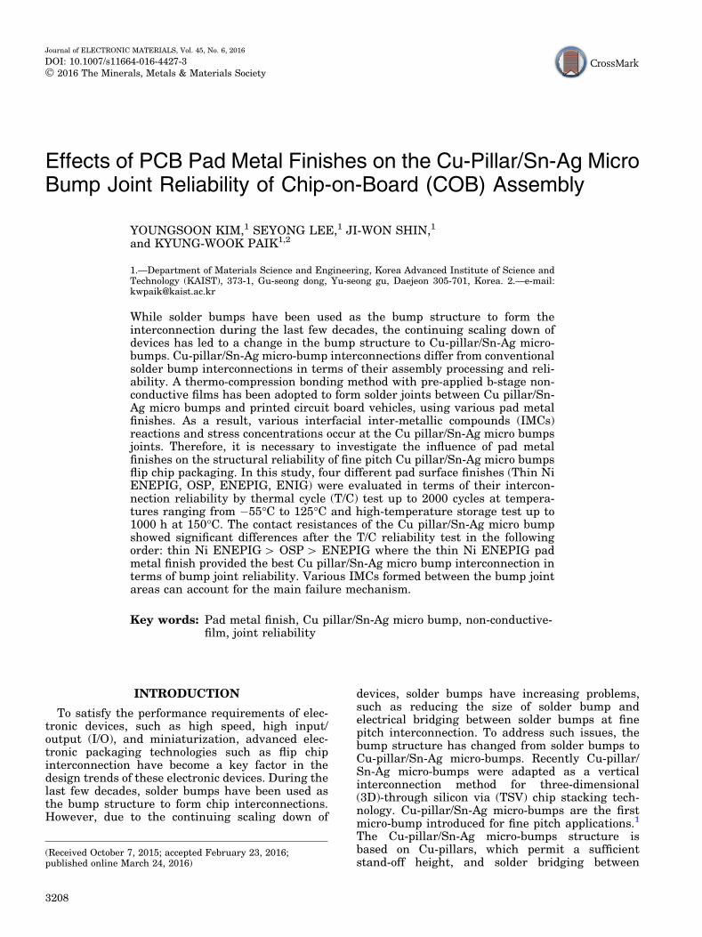
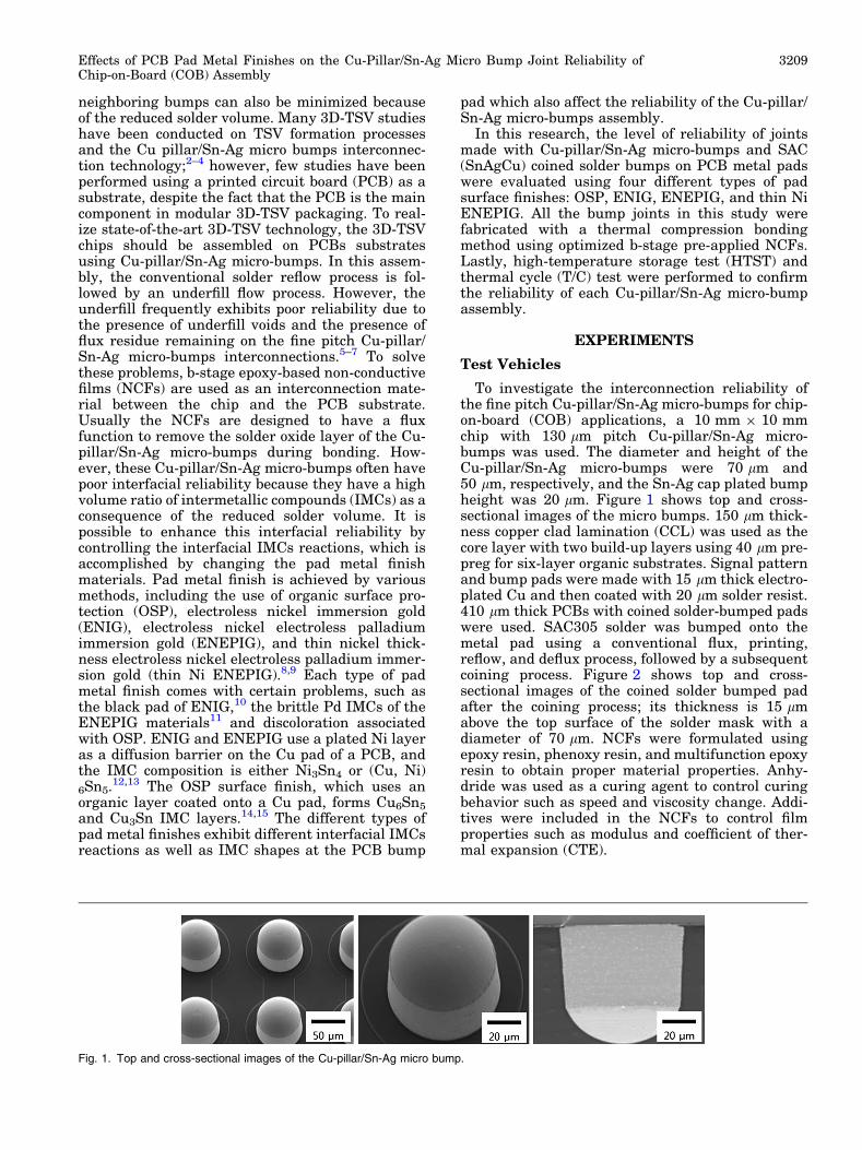
To investigate the interconnection reliability ofthe fine pitch Cu-pillar/Sn-Ag micro-bumps for chip-on-board (COB) applications, a 10 mm 9 10 mmchip with 130 lm pitch Cu-pillar/Sn-Ag micro-bumps was used. The diameter and height of theCu-pillar/Sn-Ag micro-bumps were 70 lm and50 lm, respectively, and the Sn-Ag cap plated bumpheight was 20 lm. Figure 1 shows top and cross-sectional images of the micro bumps. 150 lm thick-ness copper clad lamination (CCL) was used as thecore layer with two build-up layers using 40 lm pre-preg for six-layer organic substrates. Signal patternand bump pads were made with 15 lm thick electro-plated Cu and then coated with 20 lm solder resist.410 lm thick PCBs with coined solder-bumped padswere used. SAC305 solder was bumped onto themetal pad using a conventional flux, printing,reflow, and deflux process, followed by a subsequentcoining process. Figure 2 shows top and cross-sectional images of the coined solder bumped padafter the coining process; its thickness is 15 lmabove the top surface of the solder mask with adiameter of 70 lm. NCFs were formulated usingepoxy resin, phenoxy resin, and multifunction epoxyresin to obtain proper material properties. Anhy-dride was used as a curing agent to control curingbehavior such as speed and viscosity change. Addi-tives were included in the NCFs to control filmproperties such as modulus and coefficient of ther-mal expansion (CTE).
Fig. 1. Top and cross-sectional images of the Cu-pillar/Sn-Ag micro bump.
Effects of PCB Pad Metal Finishes on the Cu-Pillar/Sn-Ag Micro Bump Joint Reliability ofChip-on-Board (COB) Assembly
3209
Pad Metal Finish Materials
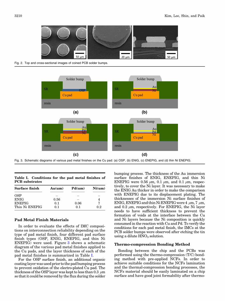
In order to evaluate the effects of IMC composi-tions on interconnection reliability depending on thetype of pad metal finish, four different pad surfacefinish types (OSP, ENIG, ENEPIG, and thin NiENEPIG) were used. Figure 3 shows a schematicdiagram of the various pad metal finishes applied tothe Cu pads, and the layer thickness of each of thepad metal finishes is summarized in Table I.
For the OSP surface finish, an additional organiccoating layerwasusedprior to thepadbumpingprocessto prevent oxidation of the electro-plated Cu pad. Thethickness of the OSP layer was kept to less than 0.3 lmso that it could be removed by the flux during the solder
bumping process. The thickness of the Au immersionsurface finishes of ENIG, ENEPIG, and thin NiENEPIG were 0.56 lm, 0.1 lm, and 0.1 lm, respec-tively, to cover the Ni layer. It was necessary to makethe ENIG Au thicker in order to make the comparisonwith ENEPIG due to its displacement plating. Thethicknesses of the immersion Ni surface finishes ofENIG,ENEPIG and thin NiENEPIG were4 lm,7 lm,and 0.2 lm, respectively. For ENEPIG, the Ni layerneeds to have sufficient thickness to prevent theformation of voids at the interface between the Cuand Ni layers because the Ni composition is quicklyconsumed in the reaction with Cu and Pd. To verify theconditions for each pad metal finish, the IMCs at thePCB solder bumps were observed after etching the tinusing a dilute HNO3 solution.
Thermo-compression Bonding Method
Bonding between the chip and the PCBs wasperformed using the thermo-compression (T/C) bond-ing method with pre-applied NCFs. In order toachieve suitable conditions for the NCFs laminationand the thermal-compression bonding processes, theNCFs material should be easily laminated on a chipsurface and have good joint formability after thermo-
Fig. 2. Top and cross-sectional images of coined PCB solder bumps.
Fig. 3. Schematic diagrams of various pad metal finishes on the Cu pad: (a) OSP, (b) ENIG, (c) ENEPIG, and (d) thin Ni ENEPIG.
Table I. Conditions for the pad metal finishes ofPCB substrates
Surface finish Au(um) Pd(um) Ni(um)
OSP � � �ENIG 0.56 � 4ENEPIG 0.1 0.06 7Thin Ni ENEPIG 0.1 0.1 0.2
Kim, Lee, Shin, and Paik3210
compression bonding with the full curing propertiesof NCFs resin after the bonding process. The thermo-compression bonding was performed at 250�C for30 s with a heating rate of 6�C/s.
Evaluation Methods
The bonded BGA modules were subjected toreliability test including a thermal cycle test and
high temperature storage tests. The thermal cycletest was performed for up to 2000 cycles withtemperature ranging from �55�C to 125�C and theHTST was performed at 150�C for up to 1000 h. Thecontact resistances of a bump joint were measuredusing a four-point probe at certain cycling periods(250 cycles, 500 cycles, 750 cycles, 1000 cycles,1500 cycles, 2000 cycles) during the thermal cycletest. In addition, joint morphologies and their
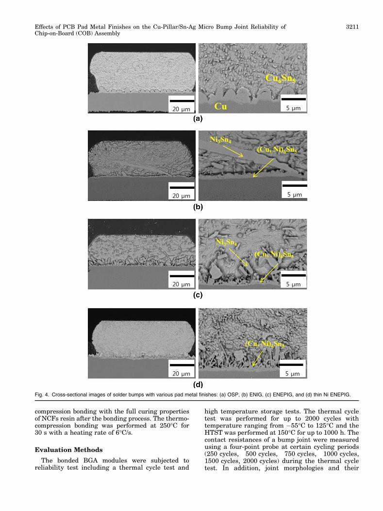
Fig. 4. Cross-sectional images of solder bumps with various pad metal finishes: (a) OSP, (b) ENIG, (c) ENEPIG, and (d) thin Ni ENEPIG.
Effects of PCB Pad Metal Finishes on the Cu-Pillar/Sn-Ag Micro Bump Joint Reliability ofChip-on-Board (COB) Assembly
3211
corresponding failure modes were investigated byscanning electron microscopy (SEM) and energydispersive x-ray spectroscopy (EDX).
RESULTS
Observation of IMCs Depending on Pad MetalFinishes
Coined solder bumps with four different padmetal finishes were observed using SEM afteretching with dilute HNO3. As shown in Fig. 4,various IMC shapes were observed depending onthe type of pad metal finishes. The OSP padsurface finish showed big Cu6Sn5 IMCs throughoutthe pad area, which was the first phase to form atthe interface between the solder and the copper.However, ENIG showed several clusters of IMCswhich grew almost to the top of the solder bump.And the ENEPIG surface finish showed smallclusters of big IMCs compared with that of ENIG.In the case of the thin Ni ENEPIG, the shapes ofthe IMCs were similar to those of the ENEPIG, butthe size of the IMCs was smaller than in ENEPIG.This difference affected the Ni thickness on thesurface finish.
Evaluation of Cu-Pillar/Sn-Ag Micro BumpJoint After a Thermal Cycle Test
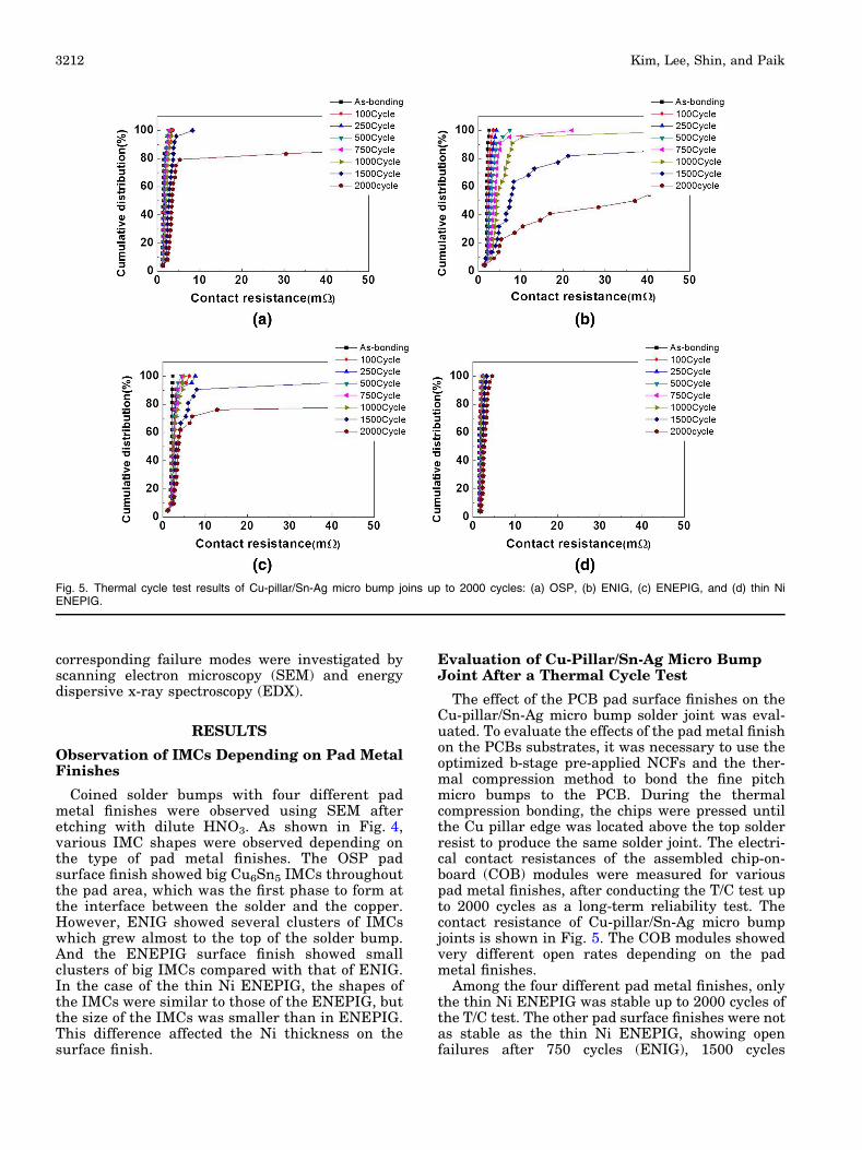
The effect of the PCB pad surface finishes on theCu-pillar/Sn-Ag micro bump solder joint was eval-uated. To evaluate the effects of the pad metal finishon the PCBs substrates, it was necessary to use theoptimized b-stage pre-applied NCFs and the ther-mal compression method to bond the fine pitchmicro bumps to the PCB. During the thermalcompression bonding, the chips were pressed untilthe Cu pillar edge was located above the top solderresist to produce the same solder joint. The electri-cal contact resistances of the assembled chip-on-board (COB) modules were measured for variouspad metal finishes, after conducting the T/C test upto 2000 cycles as a long-term reliability test. Thecontact resistance of Cu-pillar/Sn-Ag micro bumpjoints is shown in Fig. 5. The COB modules showedvery different open rates depending on the padmetal finishes.
Among the four different pad metal finishes, onlythe thin Ni ENEPIG was stable up to 2000 cycles ofthe T/C test. The other pad surface finishes were notas stable as the thin Ni ENEPIG, showing openfailures after 750 cycles (ENIG), 1500 cycles
Fig. 5. Thermal cycle test results of Cu-pillar/Sn-Ag micro bump joins up to 2000 cycles: (a) OSP, (b) ENIG, (c) ENEPIG, and (d) thin NiENEPIG.
Kim, Lee, Shin, and Paik3212
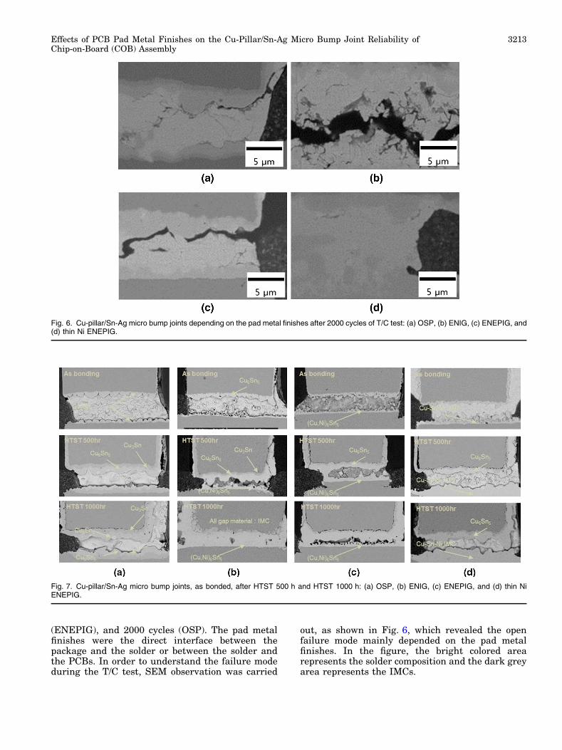
(ENEPIG), and 2000 cycles (OSP). The pad metalfinishes were the direct interface between thepackage and the solder or between the solder andthe PCBs. In order to understand the failure modeduring the T/C test, SEM observation was carried
out, as shown in Fig. 6, which revealed the openfailure mode mainly depended on the pad metalfinishes. In the figure, the bright colored arearepresents the solder composition and the dark greyarea represents the IMCs.
Fig. 6. Cu-pillar/Sn-Ag micro bump joints depending on the pad metal finishes after 2000 cycles of T/C test: (a) OSP, (b) ENIG, (c) ENEPIG, and(d) thin Ni ENEPIG.
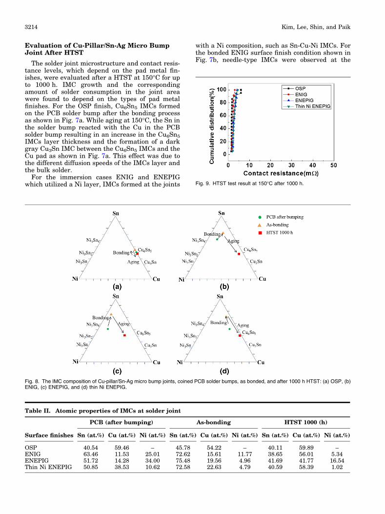
Fig. 7. Cu-pillar/Sn-Ag micro bump joints, as bonded, after HTST 500 h and HTST 1000 h: (a) OSP, (b) ENIG, (c) ENEPIG, and (d) thin NiENEPIG.
Effects of PCB Pad Metal Finishes on the Cu-Pillar/Sn-Ag Micro Bump Joint Reliability ofChip-on-Board (COB) Assembly
3213
Evaluation of Cu-Pillar/Sn-Ag Micro BumpJoint After HTST
The solder joint microstructure and contact resis-tance levels, which depend on the pad metal fin-ishes, were evaluated after a HTST at 150�C for upto 1000 h. IMC growth and the correspondingamount of solder consumption in the joint areawere found to depend on the types of pad metalfinishes. For the OSP finish, Cu6Sn5 IMCs formedon the PCB solder bump after the bonding processas shown in Fig. 7a. While aging at 150�C, the Sn inthe solder bump reacted with the Cu in the PCBsolder bump resulting in an increase in the Cu6Sn5
IMCs layer thickness and the formation of a darkgray Cu3Sn IMC between the Cu6Sn5 IMCs and theCu pad as shown in Fig. 7a. This effect was due tothe different diffusion speeds of the IMCs layer andthe bulk solder.
For the immersion cases ENIG and ENEPIGwhich utilized a Ni layer, IMCs formed at the joints
with a Ni composition, such as Sn-Cu-Ni IMCs. Forthe bonded ENIG surface finish condition shown inFig. 7b, needle-type IMCs were observed at the
Fig. 8. The IMC composition of Cu-pillar/Sn-Ag micro bump joints, coined PCB solder bumps, as bonded, and after 1000 h HTST: (a) OSP, (b)ENIG, (c) ENEPIG, and (d) thin Ni ENEPIG.
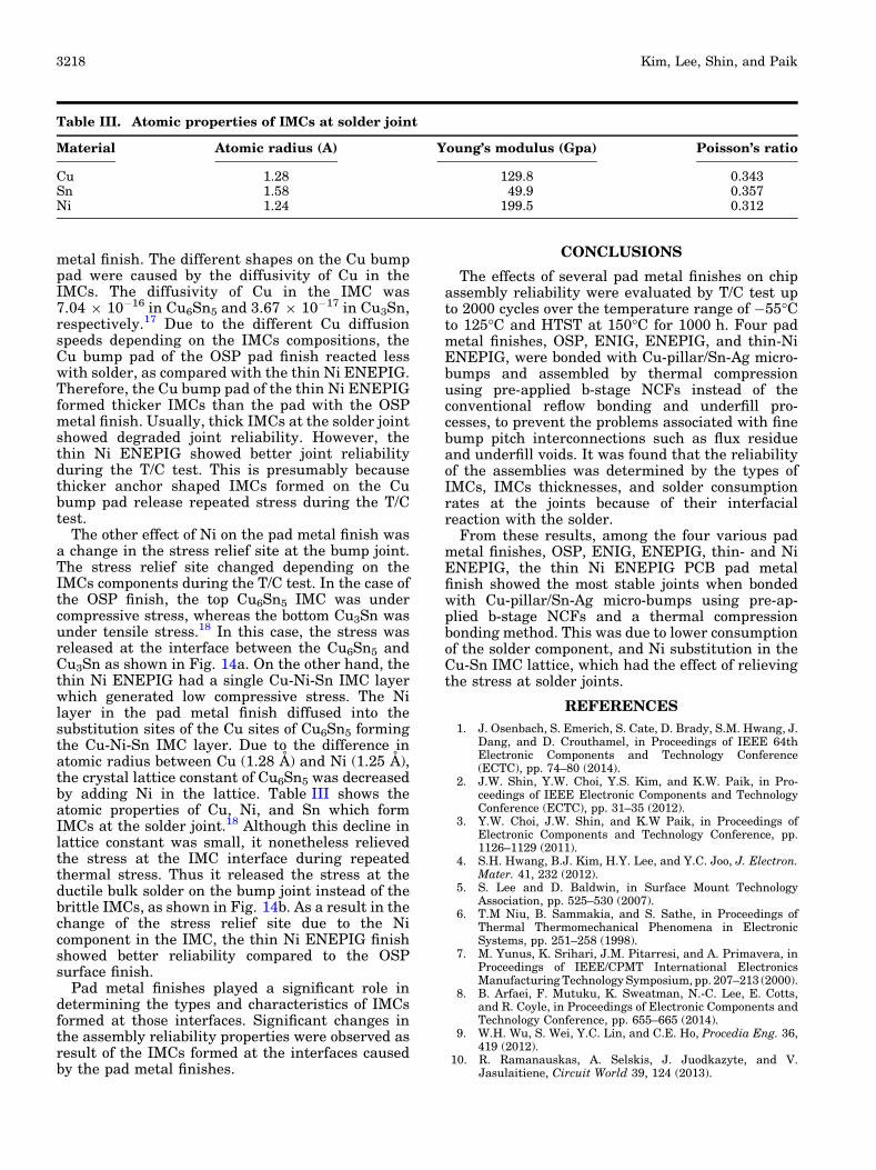
Table II. Atomic properties of IMCs at solder joint
Surface finishes
PCB (after bumping) As-bonding HTST 1000 (h)
Sn (at.%) Cu (at.%) Ni (at.%) Sn (at.%) Cu (at.%) Ni (at.%) Sn (at.%) Cu (at.%) Ni (at.%)
OSP 40.54 59.46 – 45.78 54.22 – 40.11 59.89 –ENIG 63.46 11.53 25.01 72.62 15.61 11.77 38.65 56.01 5.34ENEPIG 51.72 14.28 34.00 75.48 19.56 4.96 41.69 41.77 16.54Thin Ni ENEPIG 50.85 38.53 10.62 72.58 22.63 4.79 40.59 58.39 1.02
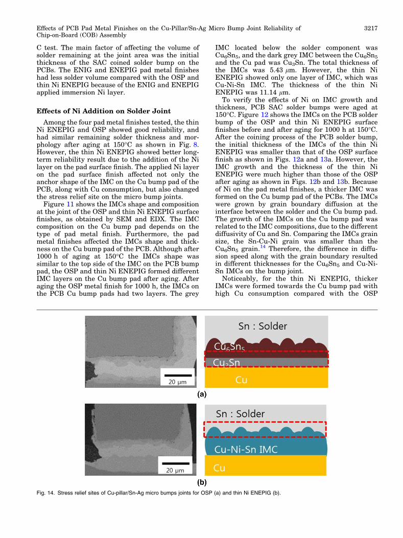
Fig. 9. HTST test result at 150�C after 1000 h.
Kim, Lee, Shin, and Paik3214

interface between the PCB solder bump pads, withthe solder bumps making contact with neighboringsolder bumps. This showed that after 1000 h ofaging the joint was fully filled with IMCs due to thelack of a diffusion layer on the pad metal finish,which allowed a thick IMC layer to form beforebonding.
The palladium layer between the Ni and Au layerson the ENEPIG surface finish acted as a diffusionbarrier layer allowing less solder consumption dur-ing the aging process as shown in Fig. 7c. Thisresulted in a thinner IMCs layer compared to that ofthe ENIG finish. However, nearly all the solder inthe solder bumps became IMCs after aging as shownin Fig. 7c. One significant observation was the jointarea morphology of the thin Ni ENEPIG, whichshowed a needle-type IMCs layer shape at the PCBbump pad after bonding. However, after aging for1000 h at 150�C, it became similar to those on theOSP surface finish as shown in Fig. 7d. The Nicomposition at the thin Ni layer diffused rapidly intothe solder joint, similar to the Au diffusion duringthe bonding process.
The composition of the IMCs on the PCB Cu padwas investigated for the different metal surfacefinishes using energy dispersive x-ray spectroscopy(EDX). Figure 8 shows the IMCs compositions onthe PCB Cu pad after PCB SAC solder bumping,after bonding with the Cu-pillar/Sn-Ag micro bump,and after HTST 1000 h. Typically, Cu6Sn5 andNi3Sn4 were the firstly formed IMCs at the interfacein the Sn-Cu and Sn-Ni binary system, respectively.On the other hand (Ni1�x,Cux)3Sn4 or(Cu1�y,Niy)6Sn5 were formed depending on Cu sol-ubility at the IMCs in the Sn-Cu-Ni ternary system.The phase changes from (Ni1�x,Cux)3Sn4 to(Cu1�y,Niy)6Sn5 were induced by the diffusion ofthe Cu contents through the (Ni1�x,Cux)3Sn4 grainboundary, and reaction with Sn and Ni to form(Cu1�y,Niy)6Sn5 IMCs. These phase changes can beproduced by small amounts of Cu. Moreover, Nidiffused with Cu6Sn5 will form (Cu,Ni)6Sn5 IMC forthe stabilized phase.16
In the case of the OSP finish, the composition ofthe IMCS on the PCB Cu pad after PCB SAC solderbumping was Cu6Sn5. The Sn content in the Cu6Sn5
IMCs was slightly increased after bonding with theCu-pillar/Sn-Ag micro bump due to Sn diffusionduring high temperature thermal compressionbonding. 1000 h aging is enough time to form Cu3Snbetween the Cu6Sn5 and the Cu pad. Because of thediffusion of the Sn and Cu contents and the reactiontype growth of IMCs, the Sn content in the Cu6Sn5
was slightly decreased, whereas the Cu content inthe Cu6Sn5 was slightly increased, as shown inFig. 8a.
In case of the immersion Ni, ENIG, ENEPIG, andthin Ni ENEPIG, Sn-Cu-Ni IMCs were formed onthe PCB Cu pad. Because of the different thicknessof plated Ni on the PCB Cu pad, the Ni content inthe IMCs after PCB SAC solder bumping was10.62 at.% (thin Ni ENEPIG), 25.01 at.% (ENIG),and 34.0 at.% (ENEPIG), respectively. After bond-ing and aging, the Sn content of the immersion Nicases showed behavior similar to the OSP surfacefinish, which increased after bonding due to Sndiffusion, and decreased after aging due to thereaction type growth of the IMCs, and Ni diffusioninto the remaining solder at the micro bump joint.On the other hand, Ni content in the IMCsdecreased after bonding due to Sn diffusion, andincreased after aging due to the diffusion of Nicontent from the plated Ni layer on the PCB Cu padinto the remaining solder at the micro bump joint insufficient time as shown in Fig. 8b–d.
The IMCs compositions of all the Ni immersionplating surface finishes, ENIG, ENEPIG, and thinNi ENEPIG, were closed to a (Ni1�x,Cux)3Sn4 com-position after PCB SAC solder bumping. However,these compositions were changed to (Cu1�y,Niy)6Sn5
due to Sn and Ni reaction by the thermal compres-sion bonding process and after aging 1000 h. ENIG,ENEPIG, and thin Ni ENEPIG showed similarphase changes before and after thermal compres-sion bonding and aging, as shown in Fig. 8b–d.Table II summarizes the Sn, Cu, and Ni content inIMCs depending on metal surface finishes afterPCB SAC solder bumping, thermal compressionbonding, and 1000 h aging.
Although the compositions and morphologies ofthe IMCs were completely dependent on the padmetal finishes, the joint contact resistances of alltest conditions were stable after aging for 1000 h at150�C as shown in Fig. 9. Moreover, fully changedIMCs were stable, and did not affect the electricalproperties of the assembly.
DISCUSSION
Investigation of Solder Bump Joint Reliability
After the T/C test, cracks were initiated at theedge of the solder resist open area, usually at thechip side, and then the crack propagated along theinterface between the IMCs and the solder
Fig. 10. Open failure rates and the remaining solder thickness ofvarious pad metal finishes after T/C cycles.
Effects of PCB Pad Metal Finishes on the Cu-Pillar/Sn-Ag Micro Bump Joint Reliability ofChip-on-Board (COB) Assembly
3215

component. Brittle fractures occurred for all the padmetal finish conditions at the interconnection areabetween the micro bump (chip side) and the SAC305of the coined solder bump on the PCB side. Whenthermal mechanical stress was applied during theT/C test, the Cu-pillar/Sn-Ag micro bump jointgenerated cracks easily at the interconnectionbecause of the different properties of the jointcomponents. The position where the cracks initiatedwas close to the component side due to the thermalstress generated during the T/C test at the inter-connection between the chip and substrate metalpads. Crack propagation was along the IMC layerbetween the Cu-pillar and the solder because of itsbrittleness compared with the bulk solder. The openfailure result of the T/C test was in good agreement
with the HTST result after 1000 h of aging as shownin Fig. 10.
The thermal cycle test result was closely relatedto the remaining solder volume at the solder joint.When sufficient solder remained, a fractureoccurred at the inside of the solder bumps, becausethe solder bumps had sufficient time for plasticdeformation during the T/C test. Therefore, lowerconsumption of solder at the joint area resulted inbetter T/C reliability. In the case of the OSP and thethin Ni ENEPIG pad metal finishes, reduced solderconsumption was observed at the joint area, whichresulted in better thermal stress reliability than theENIG and ENEPIG finishes. In the ENIG andENEPIG finishes, joint solder was mostly consumedand changed to IMCs at the joint area during the T/
Fig. 11. Cu-pillar/Sn-Ag micro bump joints after 1000 h HTST (a) OSP and (b) thin Ni ENEPIG.
Fig. 12. The interfaces between coined PCB solder bumps and OSP pad metal finish before HTST (a) and after 1000 h HTST (b).
Fig. 13. The interfaces between coined PCB solder bumps and thin Ni ENEPIG pad metal finish before HTST (a) and after 1000 h HTST (b).
Kim, Lee, Shin, and Paik3216
C test. The main factor of affecting the volume ofsolder remaining at the joint area was the initialthickness of the SAC coined solder bump on thePCBs. The ENIG and ENEPIG pad metal finisheshad less solder volume compared with the OSP andthin Ni ENEPIG because of the ENIG and ENEPIGapplied immersion Ni layer.
Effects of Ni Addition on Solder Joint
Among the four pad metal finishes tested, the thinNi ENEPIG and OSP showed good reliability, andhad similar remaining solder thickness and mor-phology after aging at 150�C as shown in Fig. 8.However, the thin Ni ENEPIG showed better long-term reliability result due to the addition of the Nilayer on the pad surface finish. The applied Ni layeron the pad surface finish affected not only theanchor shape of the IMC on the Cu bump pad of thePCB, along with Cu consumption, but also changedthe stress relief site on the micro bump joints.
Figure 11 shows the IMCs shape and compositionat the joint of the OSP and thin Ni ENEPIG surfacefinishes, as obtained by SEM and EDX. The IMCcomposition on the Cu bump pad depends on thetype of pad metal finish. Furthermore, the padmetal finishes affected the IMCs shape and thick-ness on the Cu bump pad of the PCB. Although after1000 h of aging at 150�C the IMCs shape wassimilar to the top side of the IMC on the PCB bumppad, the OSP and thin Ni ENEPIG formed differentIMC layers on the Cu bump pad after aging. Afteraging the OSP metal finish for 1000 h, the IMCs onthe PCB Cu bump pads had two layers. The grey
IMC located below the solder component wasCu6Sn5, and the dark grey IMC between the Cu6Sn5
and the Cu pad was Cu3Sn. The total thickness ofthe IMCs was 5.43 lm. However, the thin NiENEPIG showed only one layer of IMC, which wasCu-Ni-Sn IMC. The thickness of the thin NiENEPIG was 11.14 lm.
To verify the effects of Ni on IMC growth andthickness, PCB SAC solder bumps were aged at150�C. Figure 12 shows the IMCs on the PCB solderbump of the OSP and thin Ni ENEPIG surfacefinishes before and after aging for 1000 h at 150�C.After the coining process of the PCB solder bump,the initial thickness of the IMCs of the thin NiENEPIG was smaller than that of the OSP surfacefinish as shown in Figs. 12a and 13a. However, theIMC growth and the thickness of the thin NiENEPIG were much higher than those of the OSPafter aging as shown in Figs. 12b and 13b. Becauseof Ni on the pad metal finishes, a thicker IMC wasformed on the Cu bump pad of the PCBs. The IMCswere grown by grain boundary diffusion at theinterface between the solder and the Cu bump pad.The growth of the IMCs on the Cu bump pad wasrelated to the IMC compositions, due to the differentdiffusivity of Cu and Sn. Comparing the IMCs grainsize, the Sn-Cu-Ni grain was smaller than theCu6Sn5 grain.14 Therefore, the difference in diffu-sion speed along with the grain boundary resultedin different thicknesses for the Cu6Sn5 and Cu-Ni-Sn IMCs on the bump joint.
Noticeably, for the thin Ni ENEPIG, thickerIMCs were formed towards the Cu bump pad withhigh Cu consumption compared with the OSP
Fig. 14. Stress relief sites of Cu-pillar/Sn-Ag micro bumps joints for OSP (a) and thin Ni ENEPIG (b).
Effects of PCB Pad Metal Finishes on the Cu-Pillar/Sn-Ag Micro Bump Joint Reliability ofChip-on-Board (COB) Assembly
3217
metal finish. The different shapes on the Cu bumppad were caused by the diffusivity of Cu in theIMCs. The diffusivity of Cu in the IMC was7.04 9 10�16 in Cu6Sn5 and 3.67 9 10�17 in Cu3Sn,respectively.17 Due to the different Cu diffusionspeeds depending on the IMCs compositions, theCu bump pad of the OSP pad finish reacted lesswith solder, as compared with the thin Ni ENEPIG.Therefore, the Cu bump pad of the thin Ni ENEPIGformed thicker IMCs than the pad with the OSPmetal finish. Usually, thick IMCs at the solder jointshowed degraded joint reliability. However, thethin Ni ENEPIG showed better joint reliabilityduring the T/C test. This is presumably becausethicker anchor shaped IMCs formed on the Cubump pad release repeated stress during the T/Ctest.
The other effect of Ni on the pad metal finish wasa change in the stress relief site at the bump joint.The stress relief site changed depending on theIMCs components during the T/C test. In the case ofthe OSP finish, the top Cu6Sn5 IMC was undercompressive stress, whereas the bottom Cu3Sn wasunder tensile stress.18 In this case, the stress wasreleased at the interface between the Cu6Sn5 andCu3Sn as shown in Fig. 14a. On the other hand, thethin Ni ENEPIG had a single Cu-Ni-Sn IMC layerwhich generated low compressive stress. The Nilayer in the pad metal finish diffused into thesubstitution sites of the Cu sites of Cu6Sn5 formingthe Cu-Ni-Sn IMC layer. Due to the difference inatomic radius between Cu (1.28 A) and Ni (1.25 A),the crystal lattice constant of Cu6Sn5 was decreasedby adding Ni in the lattice. Table III shows theatomic properties of Cu, Ni, and Sn which formIMCs at the solder joint.18 Although this decline inlattice constant was small, it nonetheless relievedthe stress at the IMC interface during repeatedthermal stress. Thus it released the stress at theductile bulk solder on the bump joint instead of thebrittle IMCs, as shown in Fig. 14b. As a result in thechange of the stress relief site due to the Nicomponent in the IMC, the thin Ni ENEPIG finishshowed better reliability compared to the OSPsurface finish.
Pad metal finishes played a significant role indetermining the types and characteristics of IMCsformed at those interfaces. Significant changes inthe assembly reliability properties were observed asresult of the IMCs formed at the interfaces causedby the pad metal finishes.
CONCLUSIONS
The effects of several pad metal finishes on chipassembly reliability were evaluated by T/C test upto 2000 cycles over the temperature range of �55�Cto 125�C and HTST at 150�C for 1000 h. Four padmetal finishes, OSP, ENIG, ENEPIG, and thin-NiENEPIG, were bonded with Cu-pillar/Sn-Ag micro-bumps and assembled by thermal compressionusing pre-applied b-stage NCFs instead of theconventional reflow bonding and underfill pro-cesses, to prevent the problems associated with finebump pitch interconnections such as flux residueand underfill voids. It was found that the reliabilityof the assemblies was determined by the types ofIMCs, IMCs thicknesses, and solder consumptionrates at the joints because of their interfacialreaction with the solder.
From these results, among the four various padmetal finishes, OSP, ENIG, ENEPIG, thin- and NiENEPIG, the thin Ni ENEPIG PCB pad metalfinish showed the most stable joints when bondedwith Cu-pillar/Sn-Ag micro-bumps using pre-ap-plied b-stage NCFs and a thermal compressionbonding method. This was due to lower consumptionof the solder component, and Ni substitution in theCu-Sn IMC lattice, which had the effect of relievingthe stress at solder joints.
REFERENCES
1. J. Osenbach, S. Emerich, S. Cate, D. Brady, S.M. Hwang, J.Dang, and D. Crouthamel, in Proceedings of IEEE 64thElectronic Components and Technology Conference(ECTC), pp. 74–80 (2014).
2. J.W. Shin, Y.W. Choi, Y.S. Kim, and K.W. Paik, in Pro-ceedings of IEEE Electronic Components and TechnologyConference (ECTC), pp. 31–35 (2012).
3. Y.W. Choi, J.W. Shin, and K.W Paik, in Proceedings ofElectronic Components and Technology Conference, pp.1126–1129 (2011).
4. S.H. Hwang, B.J. Kim, H.Y. Lee, and Y.C. Joo, J. Electron.Mater. 41, 232 (2012).
5. S. Lee and D. Baldwin, in Surface Mount TechnologyAssociation, pp. 525–530 (2007).
6. T.M Niu, B. Sammakia, and S. Sathe, in Proceedings ofThermal Thermomechanical Phenomena in ElectronicSystems, pp. 251–258 (1998).
7. M. Yunus, K. Srihari, J.M. Pitarresi, and A. Primavera, inProceedings of IEEE/CPMT International ElectronicsManufacturing Technology Symposium, pp. 207–213 (2000).
8. B. Arfaei, F. Mutuku, K. Sweatman, N.-C. Lee, E. Cotts,and R. Coyle, in Proceedings of Electronic Components andTechnology Conference, pp. 655–665 (2014).
9. W.H. Wu, S. Wei, Y.C. Lin, and C.E. Ho, Procedia Eng. 36,419 (2012).
10. R. Ramanauskas, A. Selskis, J. Juodkazyte, and V.Jasulaitiene, Circuit World 39, 124 (2013).
Table III. Atomic properties of IMCs at solder joint
Material Atomic radius (A) Young’s modulus (Gpa) Poisson’s ratio
Cu 1.28 129.8 0.343Sn 1.58 49.9 0.357Ni 1.24 199.5 0.312
Kim, Lee, Shin, and Paik3218

11. W.H. Wu, C.S. Lin, S.H. Huang, and C.E. Ho, J. Electron.Mater. 39, 2387 (2010).
12. A. Kumar, Z. Chen, S.G. Mhaisalkar, C.C. Wong, P.S. Teo,and V. Kripesh, Thin Solid Films 504, 410 (2006).
13. A. Kumar, M. He, and Z. Chen, Surf. Coat. Technol. 198,283 (2005).
14. T. Laurila, V. Vuorinen, and J.K. Kivilahti, Mater. Sci.Eng. R 49, 1 (2005).
15. J.M. Song, Y.R. Liu, Y.S. Lai, Y.T. Chiu, and N.C. Lee,Microelectron. Reliab. 52, 180 (2012).
16. C.Y. Li and J.G. Duh, J. Mater. Res. 20, 3118 (2005).17. B. Chao, S.H. Chae, X. Zhang, K.H. Lu, J. Im, and P.S. Ho,
Acta Mater. 55, 2805 (2007).18. M. Tanaka, T. Sasaki, T. Kobayashi, and K. Tatsumi, in
Proceedings of Electronic Components and TechnologyConference, pp. 78–84 (2006).
Effects of PCB Pad Metal Finishes on the Cu-Pillar/Sn-Ag Micro Bump Joint Reliability ofChip-on-Board (COB) Assembly
3219