A Systematic, Multi-Criteria Decision Support Framework for Sustainable Drainage Design

1
PROBE2.0: A Systematic Framework forRoutability Assessment from Technology to Design
in Advanced NodesChung-Kuan Cheng, Fellow, IEEE, Andrew B. Kahng, Fellow, IEEE, Hayoung Kim, Member, IEEE,,Minsoo Kim, Student Member, IEEE, Daeyeal Lee, Student Member, IEEE, Dongwon Park, Student
Member, IEEE, and Mingyu Woo, Student Member, IEEE
Abstract—In advanced nodes, scaling of critical dimensionand pitch has not progressed at historical Moore’s Law rates.Thus, scaling boosters are explored to improve achievable power,performance, area and cost (PPAC) in new technologies. However,scaling boosters increase complexity of standard-cell architec-tures, power delivery, design rules, and other aspects of the designenablement, and may not result in design-level benefits. There-fore, design-technology co-optimization (DTCO) methodologies arerequired to evaluate design-level benefits of scaling boosters. Thekey challenge for DTCO is that large engineering efforts andlong timelines are needed to develop design enablements (e.g.,cell libraries) and perform implementation studies in order toassess technology options.
We describe a new framework that can systematically evaluatea measure of intrinsic routability, Kth, across both technologyand design choices. We focus on routability since it is a criticalfactor in the scaling of area and cost. Our framework includesrealistic standard-cell libraries that are automatically generatedusing satisfiability modulo theory (SMT) methods, and a new pinshape selection method. Routability assessments are based on thePROBE approach and an improved construction of underlyingnetlist topologies. Our experimental studies demonstrate theassessment of routability impacts for advanced-node technologyand design options. We demonstrate learning-based Kth predic-tion to reduce runtime, disk space and commercial tool licensesneeded to implement our framework. Our work enables fasterand more comprehensive evaluation of technology options earlyin the technology development process.
Index Terms—VLSI CAD, design-technology co-optimization,machine learning, pathfinding, place-and-route, routability, stan-dard cell, design enablement.
I. INTRODUCTION
W ITH the slowdown of pitch scaling in advanced tech-nology nodes, scaling boosters (e.g., buried power rails
Manuscript received August 2, 2020; revised January 14, 2021; acceptedJune 21, 2021. This work was supported in part by DARPA under GrantHR0011-18-2-0032; in part by NSF under Grant CCF-1564302; in part byQualcomm; in part by Samsung Electronics; in part by NXP Semiconductors;and in part by Mentor Graphics. This article was recommended by AssociateEditor D. Z. Pan. (Corresponding author: Minsoo Kim.)
Chung-Kuan Cheng is with the Department of Computer Science andEngineering, University of California at San Diego, San Diego, La Jolla, CA,92093 USA.
Andrew B. Kahng is with the Departments of Computer Science andEngineering, and of Electrical and Computer Engineering, University ofCalifornia at San Diego, La Jolla, CA, 92093 USA.
Hayoung Kim is with Samsung Electronics Co., Ltd., Hwaseong-si,Gyeonggi-do, South Korea.
Minsoo Kim, Daeyeal Lee, Dongwon Park and Mingyu Woo are with theDepartment of Electrical and Computer Engineering, University of Californiaat San Diego, La Jolla, CA, 92093 USA (e-mail: [email protected]).
Fig. 1: Three main stages of design-technology co-optimization (DTCO).Today, the design feedback loop takes several weeks to months.
(BPR) [33], backside power delivery networks (PDN) [4] andsupervias [14]) have become critical to improve power, perfor-mance, area and cost (PPAC) in future technologies. However,scaling boosters have complex impacts on cell architecture,design rules, and other aspects of the design enablement.Thus, holistic optimizations between process technology andchip design are required. Design-technology co-optimization(DTCO) has therefore emerged as the key methodology todecide which scaling boosters enter mass production.
DTCO has three main stages: technology, design enable-ment, and design. As shown in Fig. 1, the technology stageincludes modeling and simulation methodologies related toprocess and device technology; these span technology CAD(TCAD), optical proximity correction (OPC), design rulesand SPICE models. The design enablement stage includesother required inputs to the design process, such as standard-cell libraries, IPs and signoff environments. Last, the designstage covers front-end design, logic synthesis, place-and-route(P&R), parasitic extraction, static timing analysis and physicalverifications (design rule check, layout vs. schematic check).For purposes of this paper, technology and design enablementtogether enable the IC design process. Thus, in the remainderof our discussion we use “technology” to encompass theunion of the technology and the design enablement stages,and “design” to refer to the design stage.
The key challenge in today’s DTCO is that weeks or monthsare needed for feedback from design back to technology.This is due to the effort and latency of creating prototypedesign enablements and performing design experiments. Ourcontribution lies in automating and greatly speeding up thisfeedback loop, enabling assessment of hundreds of technology
2
options within days.Density is the overarching metric for enablement of system-
level benefits through scaling [40], and directly determines theArea and Cost aspects of PPAC. In our work, we focus onroutability implications of technology choices, since routabil-ity and density are intimately tied together. The challenge ofroutability arises as back-end-of-line (BEOL, i.e., metal layers)technology fails to scale down in step with front-end-of-line(FEOL, i.e., device layers). Also, cell heights of standard-cell architectures are a crucial lever for density scaling [35],but small standard-cell heights challenge area routing andpin accessibility. Furthermore, high BEOL resistances requiredenser power delivery networks (PDN), which occupy morerouting resources and harm routability.Contributions of This Work. The goal of our work is toenable faster and more comprehensive evaluation of technol-ogy options, early in the technology development process. Inparticular, we describe a framework for systematic assessmentof routability across the combined space of technology optionsand design enablement options.
Many measures of routability have been developed andapplied over the past decades. These span the use of congestionmaps, metrics of pin accessibility, machine learning-basedcongestion predictors, and other techniques, as we review inSection II below. However, these previous methods to assessroutability do not solve two root causes of the long feedbackloop in DTCO (Fig. 1). The first root cause is that efficientsimultaneous exploration of technology and design options inDTCO is blocked by the effort and expense of the designenablement stage. Producing layouts and characterizationsfor standard-cell libraries requires an enormous amount ofengineering cost and time, due to complex constraints such astransistor-level placement, in-cell routing, and pin accessibil-ity. Today’s DTCO relies on limited, heuristic layout synthesis(e.g., manual layout of 15-60 key cells) to assess a given set oftechnology options. The second root cause is that routabilityassessment methods have mostly focused on assessing designimplementations (e.g., to predict routability of the placement ofa particular netlist), rather than assessing design enablements.
Our present work attacks both of the above-mentionedroot causes of long design feedback loops in DTCO. To dothis, we build on two threads of recent works: (1) automaticstandard-cell layout generation using Satisfiability ModuloTheory solvers [8][25], and (2) intrinsic routability assessmentof BEOL stack options via the Kth metric [20]. We reviewthese works in Section II. Our framework is able to provideassessments of intrinsic routability across a range of technol-ogy and design parameters reflecting sub-7nm technologies.Our main contributions are summarized as follows.• We describe a systematic and complete framework to
evaluate routability across key parameters of technologyand design. Our framework is generalizable and flexible;it enables rapid evaluation of hundreds of technology anddesign enablement options within hours or days, provid-ing a valuable tool for early technology development.
• We propose a pin shape selection strategy based onthe remaining pin access (RPA) [34], along with a top-metal-only pin shape selection strategy, at our design
enablement stage. We also extend methods of [8][25]to automatically produce more realistic standard-cell li-braries (LEF format [49]) in terms of power and groundpins, contacted poly pitches (CPP) and metal pitches.
• We extend the method of [20] to assess routability acrossconfigurations of technology and design, rather thanonly BEOL stack options. We study both cell-level anddesign-level routability, and show advantages of usingknight’s tour-based artificial netlist topology generationin cell-level routability assessment. (A knight’s tour is asequence of knight’s moves in a chessboard that visitseach square exactly once. Section IV-A below explainsits use in our methodology.)
• We achieve seamless integrations with commercial P&Rtooling, via automated generation of power-groundhookups in cell layouts, and routing technology files toreflect modified design rules.
• We demonstrate accurate learning-based Kth predictionthat reduces runtime, disk storage and tool license over-heads of our framework.
Our paper is organized as follows. Section II reviewsrelated previous works. Section III gives an overview of ourframework, along with the parameterizations and other detailsof how we generate standard-cell layouts and design enable-ments. Section IV describes our methodologies for routabilityassessments and learning-based Kth prediction. Section Vshows our experimental setup, key experiments and results. Wegive conclusions and directions of future work in Section VI.
II. RELATED WORK
We now review relevant previous works. Broadly, thesecan be categorized into works on (1) standard-cell layoutgeneration and (2) routability assessment. Our review includesthe works of [8][25] and of [20] which have provided a basisfor our present work.
A. Standard-Cell Layout GenerationAutomatic Standard-Cell Layout Generation. Standard-celllayout synthesis can help library design teams explore cellarchitectures with holistic consideration of transistor place-ment, in-cell routing, complicated design rules, and pin acces-sibility. The methods of [15][43] provide co-optimization oftransistor placement and in-cell routing, but do not considersuch aspects as multi-patterning design rules that are seen inadvanced technology nodes. [9][19][26] propose standard-celllayout automation frameworks for sub-7nm technologies, butthese works incorporate multiple heuristic approaches withno guarantees of optimality. Park et al. [25] unify transistor-level placement and routing with dynamic pin allocation, andapply a satisfiability modulo theories (SMT) solver to achieveoptimal layout solutions.Pin Accessibility-Aware Standard-Cell Layout. One of themost difficult design features for standard-cell layout genera-tion is the pin accessibility, which is challenged by the limitednumber of tracks and complicated design rules. The worksof [32][42] define metrics for pin accessibility within theirobjectives for standard-cell layout optimization. Seo et al. [34]propose the remaining pin access (RPA) metric to capture pinaccess interference from access points of neighboring pins.

3
Cheng et al. [8] devise “at-least-k” Boolean constraints thatguarantee a minimum number of pin openings (access points)per pin in the cell layout.The SMT-based Standard-Cell Layout Generation of[8][25]. Our present work builds on the SMT-based parametricstandard-cell generation framework of [8][25]. This frameworktakes in three main inputs. (1) Cell architectures: number ofrouting tracks and transistor fins, and track pitches. (2) Netlist:component connectivity of library cell. (3) Design rules:parametric conditional design rules depending on cell archi-tecture. Given these inputs, a cell layout is produced that isoptimal with respect to cell area, M2 track use (routability) androuted metal length, in lexicographic order of these criteria.A unifying dynamic pin allocation (DPA) constraint integratesadditional design constraints such as transistor placement, in-cell routing, conditional design rules and pin accessibilityconstraints. This yields a constraint satisfaction formulationthat produces an optimized cell layout via a single multi-objective optimization.
We observe that these previous works do not provide nec-essary enablements of commercial standard-cell P&R, such asLEF [49] generation, PDN generation, and routing technologyfile generation. Nor do these works support control parametersfor standard-cell layout generation that are relevant in sub-7nm nodes. We describe a complete framework to supportboth standard-cell layout generation and associated P&R en-ablement. Our layout generation uses RPA-based and top-metal-only pin shape selections to improve pin accessibility.
B. Routability AssessmentRoutability is a hard constraint in the modern (fixed-die) place-and-route context. Thus, many previous works have stud-ied routability-driven placement, as well as ripup-and-reroutemethods in global routing. For example, [7][18][22][27] allpropose routability-driven placement based on congestionmaps derived from early trial or global routing. Pin accessi-bility of a given standard-cell instance also affects routability.The above-mentioned work of [34] describes pin accessibility-aware detailed placement based on the RPA metric. However,we do not focus on placement and routing optimizations, butrather on methods for assessment of routability.Routability Analysis and Prediction. Tseng et al. [38]propose a systematic framework with P&R tools to checkroutability, aiming to improve placement outcomes. The au-thors propose standard cell-level and placement-level routabil-ity scores to generate cell spacing constraints. [17] proposean optimal ILP-based detailed router and evaluate feasibility(routability) of routing clips based on an ILP solver. Theauthors of [21][29][30] use Boolean satisfiability (SAT) toanalyze routability under conditional design rules. [29][30]furthermore extract minimal unsatisfiable subsets to diagnosebottlenecks when designs are proven to be unroutable.
Several recent works propose machine learning (ML)-based routability predictions. Zhuo et al. [44] propose a newroutability prediction model based on supervised learning inplacement. The works of [6][41] predict routability based onconvolutional neural networks (CNN) and support vector ma-chines (SVM), respectively. Chan et al. [2] also propose SVM-
based routability prediction, but aim to evaluate routability forvarious BEOL stack options.The PROBE Routability Measurement Utility of [20]. Ourpresent work builds on the “PROBE” framework of [20],which gives a measure of inherent routability of BEOL stackoptions. PROBE begins with a placement solution that iseasy to route – e.g., a regular mesh placement of a meshnetlist topology. PROBE then iteratively swaps the locationsof random pairs of neighboring placed cells, progressively“tangling” the placed netlist until the routing fails with morethan some threshold number of post-route DRC violations. Thenumber of random neighbor cell swaps performed, normalizedto the number of instances in a design, is denoted by K. Thenumber of swaps beyond which routing fails is denoted asthe K threshold (Kth), and captures intrinsic routing capacity(e.g., of a given BEOL stack).
Fig. 2(a) shows the scope of PROBE. Given a placement,a set of BEOL stack options {B1, B2, ..., Bi} can be rankedin terms of routability. The framework supports two types ofplacements, shown in Fig. 3. Mesh-like placements do notreflect any specific design; they consist of an array of instancesof a given 2-input or 3-input cell. Connections are madebetween neighbors, inducing a near-meshlike netlist topology.Cell width-regularized placements are design-specific, and areproduced by commercial P&R tools. However, the standardcells in the placements are all given the same cell width toavoid illegal placements after neighbor cell swaps.
We observe that [20] is applied only to BEOL stack options,and does not cover the rich space of FEOL technology anddesign enablement options. Moreover, the near-meshlike topol-ogy can produce only a limited range of routed wirelength andRent parameter values that may not match realistic values. Theframework we describe below supports DTCO with routabilityassessment across technology and design enablement options.We use a knight’s tour-based construction that can better reflectactual design attributes.
III. THE PROBE2.0 FRAMEWORK
Our PROBE2.0 framework is shown in Fig. 2(b). It takestechnology and design parameters as primary inputs, andconsists of three major stages. (1) The standard-cell layoutgeneration stage is based on input technology parameters, andis performed using an extension of an SMT-based standard-cell layout generation [8][25]. It produces purely grid-basedpin locations and cell boundaries. (2) The design enablementstage begins with the generated standard-cell layouts, and isalso performed according to the input technology parameters.Design enablement generates LEF [49], Liberty [50] androuting technology files. LEF file generation converts theprimitive form of layouts to LEF format. The conversion con-siders real-world constraints for the stability of standard-cellcharacteristics, as detailed in Section III-D. (3) The routabilityassessment stage uses a knight’s tour-based topology as wellas open-source designs with the PROBE approach [20]. Also,Fig. 2(c) shows how the PROBE2.0 flow can be realizedwith learning-based Kth prediction, where a trained machinelearning model enables more efficient routability assessment.

4
Fig. 2: Overall flows for PROBE [20] and PROBE2.0. (a) PROBE evaluates BEOL stack options (Bi) by performing neighboring cell swaps until routing failsat a (normalized) number of swaps Kth. (b) The PROBE2.0 flow, including standard-cell layout generation [8][25], automated design enablement generation,and routability assessment with multiple P&R runs. (c) A PROBE2.0 flow using a trained learning-based model to predict Kth.
Fig. 3: Placements for PROBE [20]; (a) A mesh-like placement based ona 2-input cell. The red arrows show connections between neighbor in-stances, inducing a near-meshlike netlist topology. (b) A cell width-regularizedplacement. The orange-striped cells are considered to be neighbors of theblue-striped cell. The blue-striped cell is swapped with a randomly-selectedneighbor.
The remainder of this section describes aspects of standard-cell architecture, technology and design parameters, and de-sign enablement in our framework. Our routability assessmentand learning-based Kth prediction are explained in Section IV.
A. Standard-Cell ArchitectureFig. 4 shows a grid-based standard-cell architecture and
technology parameters of standard cells, as used in our work.We follow the 7nm standard-cell architectures in [10][39] togenerate the grid-based P&R graph with four layers TS/PC,M0, M1, and M2 as depicted in Fig. 5. TS/PC and M0layers are included in FEOL layers and M1 and M2 layers areincluded in BEOL layers. Next, we give detailed definitionsof the eight technology parameters and five design parametersthat PROBE2.0 supports as user inputs.
B. Definitions of Technology ParametersTechnology parameters include various options for process
technology as well as design enablement.(1) Fin: The number of fins for devices of standard cells. Weuse 2 and 3 for Fin [10][39].(2) CPP: Contacted poly pitch for standard cells. We use 48and 54nm for CPP [35][39].(3) MP: Metal pitch for M2 and M3 routing layers. We use24, 32 and 40nm for MP [35][39].(4) RT: The number of available M2 routing tracks for standardcells. We use 4, 5 and 6 for RT [10][39].
Fig. 4: A grid-based standard-cell architecture and technology parameters forstandard cells.
Fig. 5: Schematic view of a 7nm layout [10]. Rx denotes diffusion areas.Fins are colored in yellow. M0 and M2 are horizontal while PC (Gate), TS(Source/Drain), and M1 are vertical layers. CA, V0 and V1 are vias.
(5) PGpin: Pin types for power and ground of standard cells.We support three types of power and ground pins: M1 [39],M1+M2 [3], and BPR [33]. M1 denotes power and ground pinson the M1 layer. M1+M2 denotes power and ground pins onboth M1 and M2 layers. BPR has no power and ground pinson BEOL layers. M1 and M2 power and ground pins havewidth equal to twice the minimum width on Mx (M1, M2and M3) layers. (Thus, since minimum width and minimumspacing are each equal to half the metal pitch MP, the powerand ground pins have widths equal to the Mx pitch.) Also, inenablement of BPR, the width of M1 power pins is the sameas the minimum width of Mx. This is because commercialP&R tools require power and ground pins to be connected toPDN. Note that the M1 power and ground pins do not affectroutability since the minimum routing layer is M2.(6) CH: Cell height of standard cells, expressed as a number ofM2 routing track (T) pitches. For example, if M2 routing trackpitch is 40nm and the cell height is 240nm, then CH is 6. We

5
use and refer to standard cells with 5T, 6T, 7T and 8T [10][39]cell heights. Note that CH depends on the combination of RTand PGpin. For example, if RT is 4 and PGpin is M1, thenCH is 6. If RT is 4 and PGpin is BPR, then CH is 5.(7) MPO: The number of minimum pin openings (accesspoints) per pin. For example, if MPO is 2, every pin musthave at least two access points for the generated standard-celllayout. We use the values of 2 and 3 for MPO [8][25].(8) DR: Design rule sets. In this work, all design rules aredefined based on grids. We assume that our technologies arebased on Extreme Ultraviolet (EUV) lithography. We definethree fundamental grid-based design rules for Mx layers, DR-MAR, DR-EOL and DR-VR [8][25]; we also define two designrule sets, namely, EUV-Loose (EL) and EUV-Tight (ET).
Fig. 6 illustrates the three design rules. (i) DR-MAR denotesminimum area rules, as shown in Fig. 6(a). When a metalshape occupies only one grid point and DR-MAR is 1, thisviolates the DR-MAR rule. I.e., a metal shape must be longenough to occupy at least two routing grid points. (ii) DR-EOL denotes end-of-line rules, as shown in Fig. 6(b) and (c).When edges of two co-linear metal shapes are placed nextto each other and DR-EOL is 1, this violates the DR-EOLrule. I.e., there must be at least one unoccupied routing gridpoint between edges of metal shapes. When DR-EOL is 2,there must be at least two empty routing grid points. (iii) DR-VR denotes via restriction rules, as shown in Fig. 6(d). Thefigure shows the prohibited locations for other vias, relativeto the placement of a given via. When DR-VR is 1, only fourneighbors are blocked by the DR-VR rule.
Our two design rule sets each comprise combinations ofspecific design rule settings, as follows. EL consists of DR-MAR = 1, DR-EOL = 1, and DR-VR = 1. ET consists ofDR-MAR = 1, DR-EOL = 2, and DR-VR = 1.
Last, we note that in this work, we assume metal enclosuresof vias are 10nm in a preferred direction and 0nm in anon-preferred direction. Also, many practical design rules canbe framed using our grid-based design rules. For example,rules for end-to-end spacing and minimum enclosures can becaptured with the DR-EOL rule. We note that a wide rangeof via rules, including center, edge and corner spacing rules,can be captured with the DR-VR rule.
Fig. 6: DR-MAR, DR-EOL, and DR-VR design rules.
Based on the cell architecture of Fig. 4 and the abovetechnology parameters, our standard-cell layout generation cangenerate layouts for various cell architectures. In particular,our studies use six types of cell architectures with the combi-nations of Fin, RT and PGpin and CH shown in Table I.
TABLE I: Standard-cell architectures in our experiments.
Fin RT PGpin CH
2 4 M1/M1+M2 5BPR 6
3 5 M1/M1+M2 6BPR 7
3 6 M1/M1+M2 7BPR 8
C. Definitions of Design Parameters
Our framework uses the following design parameters.(1) BEOL: Metal stack options. We define 9M, 10M, 11Mand 13M BEOL stack options based on scaling down froma commercial 14nm technology. Recall that Mx (1X layer)pitch, i.e., MP above, is a technology parameter that we canvary in routability exploration. To scale down a 14nm BEOLtechnology to sub-7nm technologies, we define 2X, 3.2X, 9Xand 18X layer pitches based on 40nm as the 1X pitch; thisreflects advanced-node stacks as well as considerations suchas litho/cost “cliff” (∼80nm pitch limit for single-exposure193i patterning). We calculate the routing resource of [20]for each BEOL stack option. The routing resource is definedas
∑b(1/pitchb) where b denotes a metal layer and pitchb is
the pitch of b. Essentially, this sums available routing tracksover all routing layers. Table II summarizes layer counts perpitch and routing resource (R) for the BEOL stack options.(2) PDN: Power delivery network options. These include tradi-tional PDN with different layers and pitch, and backside PDNas a scaling booster for advanced technology. We define fourPDN options: Backside, Sparse, Middle and Dense. Table IIIshows the detailed information of these PDN options.(3) Tool: Commercial P&R tools [46][55], referred to only asTool A and Tool B to comply with vendor license agreements.(4) Util: Placement utilization (0.6, 0.7, 0.8).(5) Design: Designs studied in routability assessment. Weuse knight’s tour-induced artificial topologies, along with fouropen-source designs (AES, LDPC, JPEG, VGA) from Open-Cores [51]. The respective instance counts of AES, LDPC,JPEG and VGA are approximately 13K, 56K, 69K and 72K.
Table IV summarizes the technology and design parametersthat we use in our experiments. Note that in our framework,the parameter list is flexible and readily extendable. Thisenables accommodation of new technology requirements ornew scaling booster options. For example, sets of smaller CPPand MP values, including with non-unit “gear ratio” valuessuch as 2:1 or 3:2 (e.g., CPP relative to vertical M1 pitch),can be evaluated with the PROBE2.0 framework. This serves areal DTCO and technology pathfinding problem in industry forsub-3nm technologies, through the end of the lateral scalingroadmap. Also, we can easily add new designs and/or PDNstrategies as design parameters, for richer assessments.
TABLE II: Four BEOL stack options. R denotes routing resource.
BEOL 1X 2X 3.2X 9X 18X R9M 3 4 NA NA 2 104.410M 3 4 2 NA 1 117.811M 3 4 2 NA 2 120.113M 3 2 4 2 2 116.3

6
TABLE III: Details of PDN options. All numbers are pitches in units ofµm for each layer. “P” indicates that we use a given layer only for PDNat maximum area density, and do not allow the layer to be used for signalrouting. The width of M5 stripes is 0.96µm and the width of M6/M8 stripesis 1.296µm. The spacing between VDD and VSS stripes on 2X and 3.2Xlayers is 0.550µm. Backside PDN does not use any BEOL layers for PDN.
PDN 9M 10M 11M 13MBackside NA NA NA NA
Sparse
M5 10 M5 10 M5 10 M5 10M6 10 M6 10 M6 10 M8 10M8 P M9 P M10 P M12 PM9 P M10 P M11 P M13 P
Middle
M5 20 M5 20 M5 20 M5 20M6 20 M6 20 M6 20 M8 20M8 P M9 P M10 P M12 PM9 P M10 P M11 P M13 P
Dense
M5 40 M5 40 M5 40 M5 40M6 20 M6 40 M6 40 M8 40M8 P M9 P M10 P M12 PM9 P M10 P M11 P M13 P
TABLE IV: Technology and design parameters in our experiments.
Type Parameter Option
Technology
Fin 2, 3CPP 54, 48MP 24, 32, 40RT 4, 5, 6
PGpin BPR, M1, M1+M2CH 5, 6, 7, 8
MPO 2, 3DR EUV-Loose, EUV-Tight
Design
BEOL 9M, 10M, 11M, 13MPDN Backside, Sparse, Middle, DenseTool Tool A, Tool BUtil 0.6, 0.7, 0.8
Design A knight’s tour, AES, LDPC, JPEG, VGA
D. Design EnablementOur design enablement produces ready-to-use standard li-
braries and required inputs for P&R. We generate LEF formatfrom the primitive layout produced by SMT-based cell layoutgeneration. Layouts are fully grid-based, with CPP and MPtechnology parameters defining the grid pitches. Importantly,we propose two pin shape selection schemes: RPA-based pinshape selection and top-metal only pin shape selection.RPA-Based Pin Shape Selection. The SMT-generated celllayouts can have multiple distinct pin shapes for a sin-gle pin. Access to such pins must be carefully handled toavoid instability of timing and power models of the standardcells. Fig. 7(a) shows the initial SMT-generated layout of anOAI21 X1 cell. In the figure, pin ZN has two M1 shapes,ZNa and ZNb. When connections are made to different pinshapes (i.e., ZNa or ZNb), at least one of the cases will notmatch the cell’s characterized timing and power model. Forexample, when output pin ZN is connected through the M1pin shape ZNa, the cell delay is 10ps, but when the connectionis made through ZNb, the cell delay is 8ps. This instabilitywith respect to the cell timing/power model is unacceptablein modern design enablements. Therefore, when a pin hasmultiple candidate shapes, our framework chooses one of theseshapes to use in the standard-cell layout that is produced.
Given our focus on routability, we apply pin shape selectionbased on the Remaining Pin Access (RPA) pin accessibilitymetric [34]. Fig. 7 shows an example of our pin shapeselection. Accessibility of a given pin is affected by other pinswithin a distance dint. We set dint as 1.0 for the EL designrule set, and 2.0 for the ET design rule set. We then calculateRPA values for each pin shape. From [34], pin access points
A1ZNa
A2
ZNb
B
dint dint
aA2,1
aA2,2
2.0 0.83
1.0
1.0
1.5
(a)
A1ZN
A2
OBS
B
(b)Fig. 7: Example of pin shape selection in a standard cell, with Fin = 2, RT =5, MPO = 2, and the EL design rule set. (a) Initial layout of OAI21 X1 fromSMT-based layout generation, with calculated RPA values of 2.0, 0.83, 1.0,1.0 and 1.5 for ZNa, A1, A2, ZNb and B respectively. (b) The OAI21 X1layout after RPA-based pin shape selection. The ZNa pin shape becomes theonly pin shape for ZN , and ZNb becomes an obstacle (OBS).
are defined as ap,m where p is the corresponding pin (i.e.,single pin shape) and m is the position (index) in terms ofM2 routing tracks. A(p) denotes the set of access points fora given pin p. Then, N (ap,m) denotes the set of neighboringpin access points that (1) do not belong to p and (2) are withindistance dint of p on metal layer m. For example, A(A2) ={aA2,1, aA2,2} and N (aA2,2) = {aA1,2, aZNb,2} in Fig. 7(a).The used pin access (UPA) of pin p is defined as
UPA(p) =∑
ai∈A(p)
∑aj∈N (ai)
1/|A(p(aj))| (1)
Finally, RPA of pin p is defined as
RPA(p) = |A(p)| − UPA(p) (2)
For example, RPA(A2) = 2.0 − (0.5 + 0.5) = 1.0 whenwe apply Equations (1) and (2) to the example of Fig. 7(a).In the same figure, the RPA values are 2.0 and 1.0 for ZNa
and ZNb, respectively. Since the RPA value of ZNa is largerthan that of ZNb, we choose the ZNa pin shape for ZN andmake ZNb into an obstacle on M1, as shown in Fig. 7(b). Weempirically confirm the benefits of the pin shape selection forroutability, as measured by the Kth metric, in Section V-B.Top-Metal-Only Pin Shape Selection. When standard cellshave multiple pin shapes on multiple metal layers, we incorpo-rate a top-metal-only pin shape selection step. In the exampleof Fig. 8, the initial layout of the OAI21 X1 cell has threepin shapes for the ZN pin; two on M1 (and V1) and oneon M2. In this multiple-layer situation, we do not calculateRPA values for the pin shapes. Instead, we choose the M2pin shape for ZN , and the two M1 pin shapes (and V1)become obstacles. This methodology brings several benefits.(1) Replacing M1 (and V1) pin shapes with obstacles benefitsoverall pin accessibility by reducing the complexity of pinaccess: P&R tools can solve the pin access problem moreeasily and with fewer DRCs. (2) As with the above-describedpin shape selection, we avoid instability of timing and powerwith respect to characterized models. (3) Our top-metal-onlypin shape selection mitigates susceptibility to electromigration(EM) by removing M1 pin shapes (e.g., Posser et al. [31] showa cell-internal signal EM problem in accordance with outputpin position). (4) Last, changing M1 (and V1) pin shapes intoobstacles improves accessibility of other neighboring M1 pins.

7
OBS A1
M1
V1
M2
OBS
OBS
A2
B
ZN
Fig. 8: Example of standard-cell layout with top-metal-only pin shape selec-tion. We show an initial layout of AOI21 X1 with Fin = 2, RT = 5, MPO =2, and the ET design rule set. In this case, the ZN pin has only the M2 pinshape, and the M1 and V1 shapes become obstacles in red.
VDD
VSSVSS
VDD
VSS
M1 M2
A1
A2 B
VDD
ZNa ZNb A1
A2 B
ZNa ZNb A1
A2 B
ZNa ZNb
Cell boundaryM2 Track
(a) (b) (c)Fig. 9: Power and ground pin (PGpin) examples: (a) BPR, (b) M1 and (c)M1+M2. The signal pin shapes (gray) are the same regardless of PGpin.
Power and Ground Pin Generation. To make SMT-producedlayouts usable by P&R tools, power and ground pins must beadded. Fig. 9 shows how we define power and ground pins forstandard cells. As noted in Section III-B for BPR, the widthof power and ground pins is equal to the minimum M1 width.For M1 and M1+M2, it is double this width. M2 routing gridsof standard cells with BPR have an offset by half of the M2track pitch. The figure also shows how the height of standardcells is determined by the RT and PGpin parameters.Liberty and Technology File Generation. The remainingparts of our design enablement generate Liberty and technol-ogy files. We use dummy Liberty files to avoid any potentialerrors in the commercial P&R tools. Our technology filegeneration takes as inputs the technology parameters CPP,MP and DR, and converts design rules into corresponding fileformats (e.g., LEF and routing technology files) to enable useof commercial P&R tools.
IV. ROUTABILITY ASSESSMENT AND LEARNING-BASEDKth PREDICTION
We now describe how we perform both cell-level anddesign-level routability assessment using the PROBE2.0framework. Cell-level routability assessment aims to evaluatethe intrinsic routability of an individual standard cell’s layout.Design-level routability assessment uses a real design testcaseto evaluate the intrinsic routability of a design enablementand/or methodology. Recall from Section II-B that the PROBEapproach [20] starts from an initial placement of a netlist, thenprogressively increases K, the amount of “tangling”, until therouter exceeds a given DRC limit at the threshold Kth. TheKth value is specific to a given library along with technologyand design parameters. To find Kth, multiple P&R runs arelaunched with various values of K, as illustrated in Fig. 2(b).In the following, cell- and design-level routability assessments
are described in Sections IV-A and IV-B, respectively. Sec-tion IV-C describes learning-based Kth prediction to reducecompute, storage and tool license overheads.
A. Cell-Level Routability Assessment Based on Knight’s TourIn advanced technologies, pin accessibility of individual
standard-cell masters has become a critical challenge with de-creasing cell heights. We therefore propose cell-level routabil-ity assessment to evaluate routability at the individual celllevel. The previous work of [20] uses baseline mesh-likeplacements to rank BEOL stacks by routability. These in-duce nearly square-mesh netlist topologies constructed usinga single cell master from a fixed library. By contrast, ourgoal is to assess routability for a given choice of technologyand design parameters, leveraging our standard-cell generationcapability. The mesh-like placements used in [20] have keydrawbacks: (i) they do not closely reflect the wirelength andRent parameter attributes of real design testcases, and (ii) theirconstruction encompasses only 2- and 3-input cells. In thiswork, we overcome these drawbacks by using a knight’s tourto induce the initial placed netlist that is “tangled” to find Kth.
A knight’s tour is a sequence of knight’s moves that visitseach square on a chessboard exactly once. A knight movesfrom its current square to a square that is two by one (or oneby two) squares away, in any direction. In our approach, asquare in an M by N chessboard corresponds to a placed cellin an initial placement of M by N instances of a given master.A knight’s tour ordering induces connections – i.e., a netlist– within this placement. More precisely, for a given layoutregion with M rows and N columns of placed instances, anda k-input cell master, we create a knight’s tour-based topology.(1) In the layout region with M rows by N columns ofinstances, we generate a knight’s tour ordering. For this, weuse the well-known Warnsdorff-rule algorithm [45].(2) An instance of the k-input cell master that is at position iin the knight’s tour is assigned fanins from cells at positionsi−1 to i−k in the knight’s tour ordering. For a given 2-inputcell i, there will be a fanin connection from the output of celli− 1 to the first input of cell i, and a fanin connection fromthe output of cell i− 2 to the second input of cell i.(3) We end up with an initial placement (“chessboard”) havingM ×N instances, and an artificial netlist having connectionsinduced by the knight’s tour as described above.
Fig. 10 shows an example of a knight’s tour topology with2-input cells. The red arrows indicate the connections betweencell i and cell i−1. The green arrows indicate the connectionsbetween cell i and cell i− 2.
Fig. 10: Example of knight’s tour-based connections in a placement of 2-inputcells. Numbers in red circles indicate the knight’s tour ordering.

8
TABLE V: Placed design information for AES, mesh-like placements andknight’s tour based topologies. Mesh-like placements and knight’s tours have115 × 115 placed instances. Area denotes sum of instance area in the designs.Area is in units of µm2 and wirelength (WL) is in units of µm. 1-input and4-input cells are not supported by the mesh-like placement construction.
Design Cell Area #Insts WLAES - 1088 13221 46880
Mesh
INV X1 Not supportedNAND2 X1 799 13225 11001NAND3 X1 999 13225 13932NAND4 X1 Not supported
Knight’s Tour
INV X1 599 13225 10264NAND2 X1 799 13225 23610NAND3 X1 999 13225 41103NAND4 X1 1199 13225 62251
TABLE VI: Rent parameters for mesh-like and knight’s tour-based placednetlists. We show ranges of Rent parameters obtained from placements byusing [52]. We use rectangle sampling-based methods I and II for theevaluation method, Types I and II for the pin counting method, and geometricmean for the averaging method in [52]. We show designs from OpenCores [51]and the same (mesh-based, knight’s tour) placements as in Table V.
Source Design Rent Parameter
OpenCores [51]
AES [0.726, 0.832]JPEG [0.617, 0.813]VGA [0.656, 0.879]LDPC [0.812, 0.891]
PROBE [20] Mesh (NAND2 X1) [0.530, 0.535]Mesh (NAND3 X1) [0.500, 0.585]
PROBE2.0 Knight’s tour (NAND2 X1) [0.676, 0.761]Knight’s tour (NAND3 X1) [0.708, 0.820]
Our studies confirm improved flexibility and correspon-dences to real design netlists when we apply the knight’stour-based approach. Table V shows placed wirelengths of theAES design, and of mesh-like placements [20] and knight’stour-induced netlists. INV X1, NAND2 X1, NAND3 X1 andNAND4 X1 cell masters are used, with default technology anddesign parameters as specified in Section V-A. Particularlywhen based on the NAND3 X1 master, the knight’s tourtopologies can give more realistic wirelengths than mesh-like placements. (As noted above, the mesh-like placementconstruction does not support use of 1- or 4-input cell masters.)
We also note that mesh-like placements have a simple topol-ogy wherein connections are only between neighbor cells inthe initial placement. This inflexibility can weaken correspon-dences to real-world designs. Notably, the Rent parameter p ofthe (2-dimensional) mesh topology is 0.5 [16][24] accordingto Rent’s rule. We have studied achievable Rent parametersfor mesh-like placements and knight’s tour-based topologiesby using RentCon [52]. Table VI shows that Rent parametersof real circuits (AES, LDPC, JPEG, VGA) range from 0.617to 0.891. On the other hand, the mesh-like placements pvalues from 0.500 to 0.585, while our proposed knight’s tour-based placements have p values from 0.676 to 0.820. Again,the knight’s tour construction can more closely reflect realcircuits. Based on these studies, we use the knight’s tour-basedtopology construction in our cell-level routability assessment.
B. Design-Level Routability AssessmentTo perform design-level routability assessments, we begin
with open-source RTL designs from OpenCores [51] anduse commercial logic synthesis to obtain gate-level netlists.Following [20], we evaluate design-level routability based oncell width-regularized placements (Fig. 3(b)) of these netlists.
For each standard-cell library, we modify LEF such that allcombinational cells are bloated to have the same width as themaximum-width cell among all 38 combinational cells in thelibrary. (Our designs also instantiate D flip-flops, which havethe largest cell width in our generated standard-cell libraries.We fix the locations of flip-flops in designs after placementand do not swap them.)
Cell width regularization is proposed in the work of [20].Its purpose is to avoid illegal placements (with cell overlap)when neighbor cells are swapped during “tangling”. Withoutthe cell width regularization, the neighbor-cell swap operationsmight cause cell overlap due to different cell widths. Of course,the standard P&R flow does not use width-regularized cells,which raises the question of whether use of bloated cells couldlead to misleading design-level routability assessments. Ourexperimental study of Kth obtained with bloated cells, versusmaximum achievable utilization obtained with unbloated cells,is reported below in Section V-E and offers some reassurancein this regard. Aside from this, we use bloated cells for twomain reasons. (1) Our cell-level routability assessment focuseson intrinsic routability of cell layouts without any bloating ofcell widths. (2) Despite the extra widths of cells, we can stillassess pin accessibility for cells. Bloated cells still retain theiroriginal order and shapes of pins. So, the intrinsic routabilityfor standard cells can still be measured. Below, design-levelroutability assessments with various technology and designparameters are reported in Sections V-D and V-E.
C. Learning-Based Kth PredictionAlthough Kth provides a useful means of routability as-
sessment, it has three potential logistic disadvantages: largeruntimes, large data footprints, and high consumption of com-mercial EDA licenses. First, as we perform neighbor-swaps toincrease routing difficulty for a given placement, the increasingnumber of DRCs leads to large runtimes. This is becauseP&R tools perform increasingly expensive search-and-repairiterations in the detailed router. Furthermore, although we seta maximum runtime per each P&R run,1 our overall runtimeburden is still large, since the total number of tools runs itselfis large. For example, when we perform P&R with K = 1 to30 to obtain Kth, and there are just 100 sets of standard-celllibraries to be evaluated, up to 3000 P&R runs are required forthis assessment. Second, large amounts of disk space may beused by our framework. For example, just 3000 runs of P&Rwith the VGA design occupy around 300GB of disk spacein our experiments. Third, in many contexts the number ofavailable commercial P&R tool licenses will also be limited.
To mitigate these potential disadvantages, we have devel-oped learning-based Kth prediction. That is, to reduce thenumber of tool runs (thus saving runtime, disk space andlicense usage), we predict Kth via machine learning (ML)techniques, without performing all P&R runs. Fig. 2(b) and (c)show PROBE2.0 flows without, and with, Kth prediction. Theflow without Kth prediction in Fig. 2(b) requires generation
1We assume that runs with #DRCs under/around the threshold are finishedwithin the maximum runtime. We set maximum runtimes based on the instancecounts of the designs. In this work, we use maximum runtimes of two hoursfor a knight’s tour and AES, and three hours for LDPC, JPEG and VGA.

9
TABLE VII: Input features of the Kth prediction.
Type Name Data Notes
Technology
CPP IntegerMP Integer
PGpin Category BPR, M1, M1+M2CH Integer
MPO IntegerDR Category EL, ET
Design
BEOL IntegerPDN Category Backside, Sparse, Middle, DenseTool Category Tool A, Tool BUtil Float [0.0, 1.0]Inst IntegerNet Integer
steps and multiple P&R runs. On the other hand, the flowwith prediction in Fig. 2(c) finds Kth using only inferencewith a trained ML model. We use 12 input features in our MLmodeling, based on the technology and design parameters inSections III-B and III-C, respectively. Table VII summarizesthe types, names, and data types of the input features that weuse in the Kth prediction. From the original set of technologyparameters, we omit Fin and RT from our feature list sinceFin and RT are derivable from PGpin and CH. From theoriginal set of design parameters given in Section III-C, weomit “Design” and add the number of instances (Inst) and thenumber of nets (Net) as design features in our model.
We present our experimental results for the ML-based Kth
prediction in Section V-F. Importantly, our ML models aretrained in less than an hour using approximately 1968 datapoints (80% out of a total of 2460 data points); inference thenrequires only seconds for any technology-design parametercombination. By contrast, collecting a single Kth value fora given technology-design parameter combination requiresnot only the generation of standard-cell layouts and designenablements, but also up to 30 P&R runs that each consumesignificant average and maximum tool runtimes of 0.4 and3.0 hours, respectively. Thus, runtime overhead is 12 (resp.90) hours on average (resp. at most) per Kth value. In lightof such large runtimes, the primary goal of our ML-basedKth prediction is to reduce the number of required P&Rruns by predicting unseen data (that is, Kth values) withreasonably small errors. In Section V-F below, we also performan experiment to show the tradeoff of model accuracy versustraining data overheads.
V. EXPERIMENTAL SETUP AND RESULT
We demonstrate routability assessment capability ofPROBE2.0 via five main experiments.• Expt. 1: Cell-level assessment with a knight’s tour.• Expt. 2: Design-level assessment with technology param-
eters.• Expt. 3: Design-level assessment with design parameters.• Expt. 4: Achievable utilization study with Kth results.• Expt. 5: Learning-based Kth prediction.We first show routability assessments using the PROBE2.0
framework. Expt. 1 demonstrates evaluation of cell-levelroutability using our knight’s tour-based assessment. Expts.2 and 3 perform design-level routability assessments withvarious technology and design parameters (Sections III-Band III-C). Next, Expt. 4 studies achievable utilization in
TABLE VIII: List of 39 standard cells per generated library.
Cell List SizeInverter (INV), Buffer (BUF) X1, X2, X4, X8
2-input AND/OR/NAND/NOR (AND2/OR2/NAND2/NOR2) X1, X23-input AND/OR/NAND/NOR (AND3/OR3/NAND3/NOR3) X1, X2
4-input NAND/NOR (NAND4/NOR4) X1, X22-1 AND-OR-Inverter (AOI21), 2-2 AND-OR-Inverter (AOI22) X1, X22-1 OR-AND-Inverter (OAI21), 2-2 OR-AND-Inverter (OAI22) X1, X2
2-input MUX/XOR (MUX2/XOR2), D flip-flop (DFF) X1
relation to the Kth routability metric, across a range of gen-erated standard-cell libraries. Last, Expt. 5 demonstrates howlearning-based Kth prediction can mitigate potential logisticaloverheads of our framework.
A. Experimental SetupWe generate 39 cells (38 combinational and 1 sequential) for
each standard-cell library that we study, as listed in Table VIII.We name cells according to functionality, number of inputs,and size. For example, INV X1 is an X1-sized inverter, andAND3 X2 is an X2-sized 3-input AND gate. Our SMT-basedstandard-cell layout generation tool is open-sourced in [53].
Our experiments are based on a commercial 14nm tech-nology. We modify design rules of Mx (M1, M2 and M3)layers (and of vias above) in routing technology files to enablescaling to sub-7nm technologies. We draw FEOL and BEOL(Mx) layer parameters from [10][39] (see Section III-A). Layerparameters and rules for M4 and above are drawn from the14nm technology. For example, we choose the 9M (9-layer)BEOL stack option from the 14nm technology, and modifyrules for the Mx layers (M1, M2, M3). We use existingdesign rules for the upper layers (M4 to M9). Mx layers areconstrained to use unidirectional and min-width routing forstandard-cell layout generation and P&R. We also assume thatM1 is unavailable for signal routing.
All design rules are described in LEF format and routingtechnology file format [55] for use by commercial P&Rtools. SMT-generated standard-cell layouts are converted intoLEF format. For cell-level routability assessments, we usea knight’s tour with 50 by 50 instances, constructed usingan open-sourced implementation of the Warnsdorff-rule algo-rithm [45]. For design-level assessments, we perform synthesisby using a commercial tool [54] and P&R by using twocommercial P&R tools [46][55].
We also use GNU parallel [47] to perform multiple eval-uations in parallel. We assume that our designs with #DRCsless than the threshold finish within three hours. Setting themaximum runtime in GNU parallel reduces the total runtimeof the framework. We use 500 DRCs as the DRC threshold todetermine Kth. (The work of PROBE [20] used a thresholdof 150 DRCs. We set the higher threshold of 500 DRCssince SMT-generated standard-cell layouts might not be aswell-optimized for pin accessibility as mature libraries fromindustry.) Finally, we set default parameters as shown inTable IX. In all of our experiments, when not otherwisespecified, we use these pre-defined default parameters.
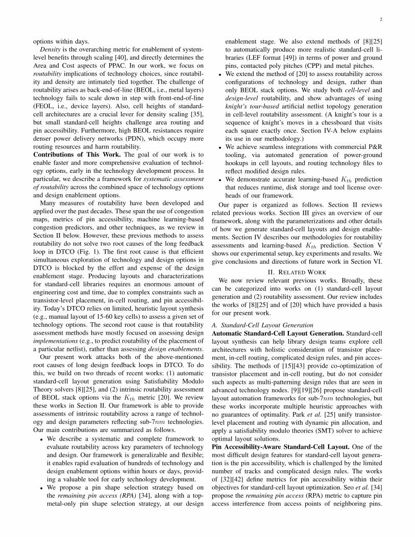
B. Expt. 1: Cell-Level Assessment with a Knight’s TourIn this experiment, we perform knight’s tour-based cell-
level routability assessments. To show Kth of standard cells
10
TABLE IX: Default parameters in our experiments.
Design Parameter Technology ParameterName Value Name Value
Fin 3 BEOL 10MCPP 54 PDN MiddleMP 40 Tool ART 5 Util 0.7
PGpin M1 Design AESCH 7 - -
MPO 2 - -DR EL - -
TABLE X: Kth results with RPA-Best and RPA-Worst pin shape selectionmethods. This table shows the Kth values corresponding to the data shownin Fig. 12.
CH Cell Kth
RPA-Best RPA-Worst
6T
AOI22 X2 11 0NAND3 X2 18 16NAND4 X2 11 10NOR3 X2 21 20NOR4 X2 14 13OAI21 X1 2 2
7T AOI21 X2 28 27OAI21 X2 28 27
with various cell heights, we draw cells from 6T, 7T and 8Tlibraries. Among the library cells, we choose 15 combinationalcells that have X1 size and more than one input pins.
Fig. 11 shows Kth results from the cell-level routabilityassessment. From the results, we observe larger Kth as cellheight increases. Also, by examining Kth per cell, we cansee which cell types are routing-critical. For example, 4-inputcells have relatively small values of Kth according to thisexperiment. Thus, at an early stage of technology development,cell-specific Kth is a promising indicator to determine whichcells need to be improved in terms of routability.
We also show the benefit of our RPA-based pin selection.We generate standard-cell layouts using two pin shape selec-tion methods, RPA-Best and RPA-Worst. RPA-Best denotes ourproposed RPA-based pin shape selection which chooses thepin shape with the largest RPA value. To show that RPA-Best brings meaningful benefits, we also create standard-celllibraries by choosing a pin shape per pin that has smallest RPAvalue; this yields the RPA-Worst method. We study six cellsfrom 6T libraries and two cells from 7T libraries. We performcell-level routability assessments on RPA-Best and RPA-Worstversions of these standard cells.
Fig. 12 plots the number of DRCs versus K, for the eightstandard cells with different pin shape selection methods. Also,Table X shows the Kth values for each standard cell. Sevenstandard cells (out of eight cells) with RPA-Best show largerKth than those with RPA-Worst. One cell (OAI X2) showsthe same Kth for both methods. We see that our RPA-basedpin shape selection helps to improve the routability.
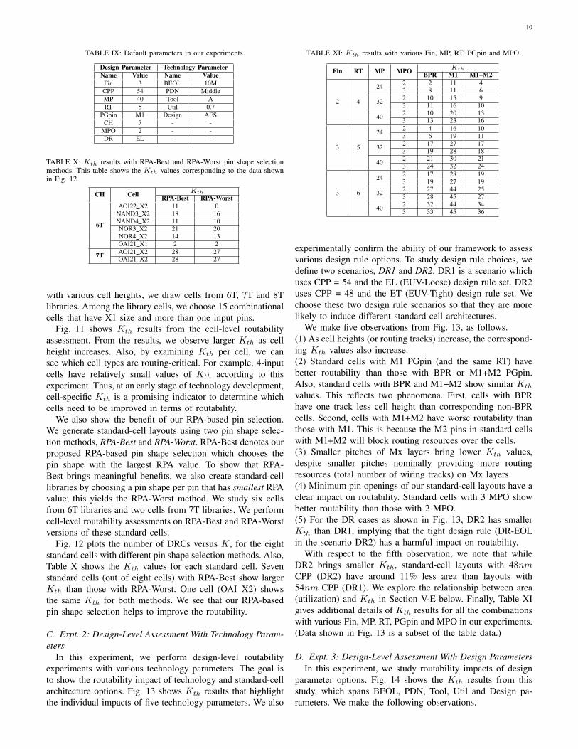
C. Expt. 2: Design-Level Assessment With Technology Param-eters
In this experiment, we perform design-level routabilityexperiments with various technology parameters. The goal isto show the routability impact of technology and standard-cellarchitecture options. Fig. 13 shows Kth results that highlightthe individual impacts of five technology parameters. We also
TABLE XI: Kth results with various Fin, MP, RT, PGpin and MPO.
Fin RT MP MPO Kth
BPR M1 M1+M2
2 4
24 2 2 11 43 8 11 6
32 2 10 15 93 11 16 10
40 2 10 20 133 13 23 16
3 5
24 2 4 16 103 6 19 11
32 2 17 27 173 19 28 18
40 2 21 30 213 24 32 24
3 6
24 2 17 28 193 19 27 19
32 2 27 44 253 28 45 27
40 2 32 44 343 33 45 36
experimentally confirm the ability of our framework to assessvarious design rule options. To study design rule choices, wedefine two scenarios, DR1 and DR2. DR1 is a scenario whichuses CPP = 54 and the EL (EUV-Loose) design rule set. DR2uses CPP = 48 and the ET (EUV-Tight) design rule set. Wechoose these two design rule scenarios so that they are morelikely to induce different standard-cell architectures.
We make five observations from Fig. 13, as follows.(1) As cell heights (or routing tracks) increase, the correspond-ing Kth values also increase.(2) Standard cells with M1 PGpin (and the same RT) havebetter routability than those with BPR or M1+M2 PGpin.Also, standard cells with BPR and M1+M2 show similar Kth
values. This reflects two phenomena. First, cells with BPRhave one track less cell height than corresponding non-BPRcells. Second, cells with M1+M2 have worse routability thanthose with M1. This is because the M2 pins in standard cellswith M1+M2 will block routing resources over the cells.(3) Smaller pitches of Mx layers bring lower Kth values,despite smaller pitches nominally providing more routingresources (total number of wiring tracks) on Mx layers.(4) Minimum pin openings of our standard-cell layouts have aclear impact on routability. Standard cells with 3 MPO showbetter routability than those with 2 MPO.(5) For the DR cases as shown in Fig. 13, DR2 has smallerKth than DR1, implying that the tight design rule (DR-EOLin the scenario DR2) has a harmful impact on routability.
With respect to the fifth observation, we note that whileDR2 brings smaller Kth, standard-cell layouts with 48nmCPP (DR2) have around 11% less area than layouts with54nm CPP (DR1). We explore the relationship between area(utilization) and Kth in Section V-E below. Finally, Table XIgives additional details of Kth results for all the combinationswith various Fin, MP, RT, PGpin and MPO in our experiments.(Data shown in Fig. 13 is a subset of the table data.)
D. Expt. 3: Design-Level Assessment With Design ParametersIn this experiment, we study routability impacts of design
parameter options. Fig. 14 shows the Kth results from thisstudy, which spans BEOL, PDN, Tool, Util and Design pa-rameters. We make the following observations.
11
Fig. 11: Kth results from knight’s tour-based cell-level routability assessments across various track heights and cell masters. 15 cell masters from 6T, 7T and8T standard-cell libraries are used in this experiment.
Fig. 12: Cell-level routability assessments showing #DRCs versus K withdifferent pin shape selection methods. Six 6T and two 7T standard cells withRPA-Best (B) and RPA-Worst (W) pin shape selection methods are shown.Solid lines are for cells with RPA-Best, and dashed lines are for cells withRPA-Worst. Table X shows the corresponding Kth values for each case.
Fig. 13: Design-level assessments with various technology parameters.
(1) According to the Kth values with the various BEOLstack options, 10M has better routability than 9M, and 11Mhas better routability than 10M. Also, 10M and 11M havebetter routability than 13M. As shown in Table II, the routingresources of 10M and 11M are larger than those of 13M.This illustrates how overall routing capacity can worsen evenif the number of metal layers is increased. However, theadditional layers bring other benefits. For example, we mayimplement a denser, more robust PDN resulting in betterdesign performance due to less resistivity of wide metal layers.(2) As fewer layer resources are used for PDN, the resultsshow better routability.(3) The Kth results from Tool A dominate those of Tool B.In this sense, our framework also has the ability to evaluateplacers and routers, as does the previous work of [20].(4) As Util increases, the Kth values decrease since routingwith denser placements is more difficult.(5) The base designs used in the design-level routability
assessments also affect the results. In particular, designs withlarger instance counts have smaller Kth. This is expected: fora given amount of “tangling” (K), and all else being equal,a larger design’s placement is expected to have more routing#DRCs. ([20] gives a probabilistic analysis of routing hotspotsand routing failure according to the number of instances.)
Fig. 14: Kth results of design-level routability assessments with variousdesign parameters.
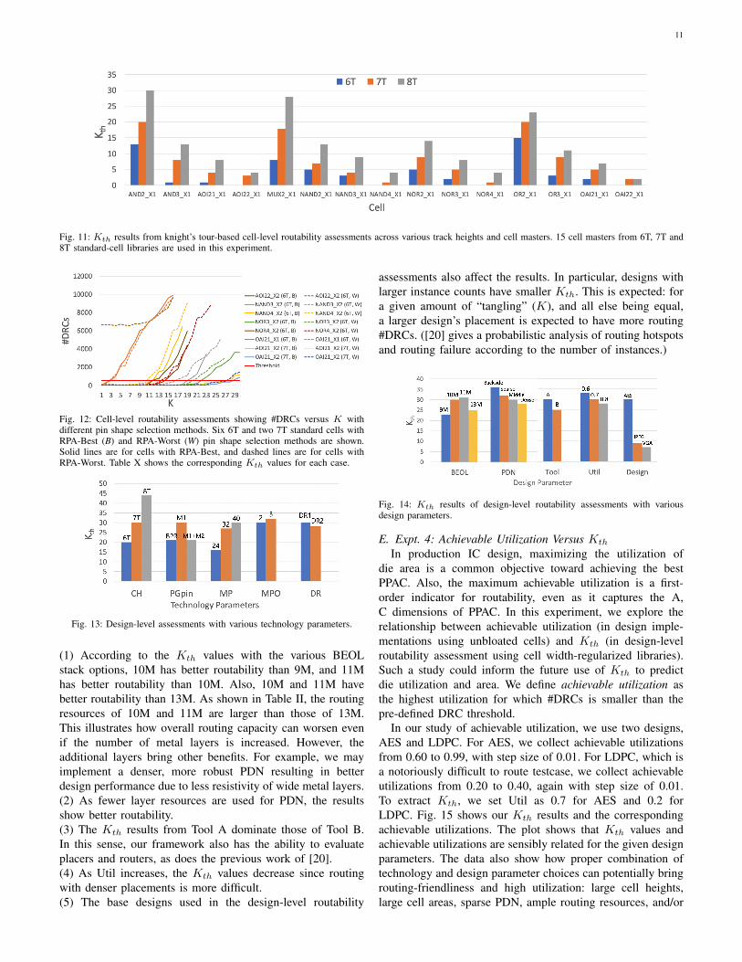
E. Expt. 4: Achievable Utilization Versus Kth
In production IC design, maximizing the utilization ofdie area is a common objective toward achieving the bestPPAC. Also, the maximum achievable utilization is a first-order indicator for routability, even as it captures the A,C dimensions of PPAC. In this experiment, we explore therelationship between achievable utilization (in design imple-mentations using unbloated cells) and Kth (in design-levelroutability assessment using cell width-regularized libraries).Such a study could inform the future use of Kth to predictdie utilization and area. We define achievable utilization asthe highest utilization for which #DRCs is smaller than thepre-defined DRC threshold.
In our study of achievable utilization, we use two designs,AES and LDPC. For AES, we collect achievable utilizationsfrom 0.60 to 0.99, with step size of 0.01. For LDPC, which isa notoriously difficult to route testcase, we collect achievableutilizations from 0.20 to 0.40, again with step size of 0.01.To extract Kth, we set Util as 0.7 for AES and 0.2 forLDPC. Fig. 15 shows our Kth results and the correspondingachievable utilizations. The plot shows that Kth values andachievable utilizations are sensibly related for the given designparameters. The data also show how proper combination oftechnology and design parameter choices can potentially bringrouting-friendliness and high utilization: large cell heights,large cell areas, sparse PDN, ample routing resources, and/or
12
0.1
0.2
0.3
0.4
0.5
0.6
0.7
0.8
0.9
1
0 10 20 30 40 50
Ach
ieva
ble
Utiliz
atio
n
Kth
2MPO_BPR
2MPO_M1
2MPO_M2
3MPO_BPR
3MPO_M1
3MPO_M2
0.2
0.3
0.4
3 8 13 18
LDPC design
LDPC
AES
Kth
Util
5T
6T7T
Fig. 15: Comparison between Kth and achievable utilization for the AESand LDPC designs. The plot shows three instances of each icon. Left to right,these correspond respectively to 5T, 6T and 7T cells for BPR, and to 6T,7T and 8T cells for M1 and M2. (To help clarify this, we give 5T, 6T and7T labels for 3MPO BPR cell libraries.) For AES, we use the same settingsas in Table IX. For LDPC, we set Util = 0.2 and enable M1 routing whenextracting Kth and achievable utilization. (LDPC has much lower achievableutilization than AES due to its complex routing topology.)
relaxed design rules all lead to routability with maximumutilization. Especially, in the enlarged view of LDPC designplot, we observe similar tendencies as seen in Fig. 13. Forexample, the cells with M1 PGpin have better Kth comparedto cells with M2 and BPR. Also, both Kth values andachievable utilizations gradually increase with cell heights.The cells with 2MPO and 3MPO have similar Kth valuesand achievable utilizations. This experiment hints that Kth
could be useful in a predictor of design-specific achievableutilization. We leave this possibility for future work.
F. Expt. 5: Learning-Based Kth PredictionWe now show results from our learning-based Kth predic-
tion. We compile a dataset of 2460 Kth values correspondingto a wide range of settings for the various features describedin Table IV. We use the open-source AutoML package [48]to predict Kth. AutoML has a hyperparameter tuning abil-ity on various models including gradient boosting machine(GBM) [12], XGBoost [5], distributed random forest (DRF),extremely randomized tree (XRT) [13], deep learning (DL) andgeneralized linear model (GLM) [28]. AutoML also suggestscombined models that outperform a single model.
We down-sample and up-sample our data since the dataare imbalanced in terms of Kth distributions.2 We use 60 as atarget sample number to generate balanced data. We randomlypartition our augmented (i.e., after sampling schemes areapplied) dataset as 80% used for training and 20% used fortesting. We perform all experiments using an Intel Xeon Gold6148 2.40GHz server (80 threads) with 256GB RAM.
We use the 3.30.0.6 version of AutoML to train our models,with default input parameter settings for AutoML. The defaultsettings of AutoML include nfolds = 5 for cross-validation,leaderboard frame = testing set, and sort metric = meanresidual deviance to rank the trained regression models. Detailsof these settings are found at [48]. We set the training timelimit as one hour with 80 threads. The suggested models from
2When generated standard cells are not routing-friendly, routing for designsthat use those cells might be infeasible. This causes the observed distributionof Kth values to be biased toward zero. The down-sampling and up-samplingschemes help us to avoid over-fitting in the prediction of Kth.
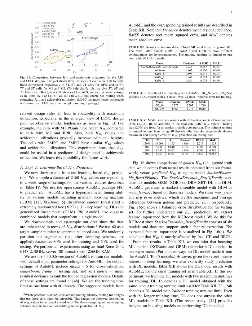
AutoML and the corresponding trained results are described inTable XII. Note that Deviance denotes mean residual deviance,RMSE denotes root mean squared error, and MAE denotesmean absolute error.
TABLE XII: Results on training data of Top-5 ML models by using AutoML.The three GBM models (GBM 1, GBM 2 and GBM 3) have differentconfigurations for hyperparameters. The training runtime is limited to onehour with 80 CPU threads.
Model Deviance RMSE MAEStackedEnsemble BestOfFamily 0.733 0.857 0.353
XGBoost 0.865 0.930 0.300GBM 1 0.896 0.947 0.374GBM 2 0.947 0.973 0.350GBM 3 0.950 0.975 0.440
TABLE XIII: Results of DL modeling with AutoML. DL 1h (resp. DL 24h)denotes a DL model with a 1-hour (resp. 24-hour) runtime limit for training.
Model Deviance RMSE MAEDL 1h 6.275 2.505 1.789DL 24h 1.469 1.212 0.615
TABLE XIV: Model accuracy results with different amounts of training data(TD), i.e., 20, 40, 60 and 80% of the total data (2460 Kth values). Testingdata (20%) are fixed for an apples-to-apples comparison. The training runtimeis limited to one hour using 80 threads. ME and AE respectively denotemaximum and average error of Kth prediction on testing data.
TD ME AE Deviance RMSE MAE20% 14.696 1.155 4.916 2.217 1.15540% 8.131 0.610 1.702 1.304 0.61060% 8.553 0.392 1.006 1.003 0.39280% 8.459 0.353 0.733 0.857 0.353
Fig. 16 shows comparisons of golden Kth (i.e., ground truthdata which comes from actual results obtained from our frame-work) versus predicted Kth using the model StackedEnsem-ble BestOfFamily. The StackedEnsemble BestOfFamily con-tains six models: GBM, XGBoost, DRF, XRT, DL and GLM.AutoML generates a stacked ensemble model with GLM asmeta learner, based on those six models. We show max errorand avg error metrics, which are the maximum and averagedifference between golden and predicted Kth, respectively.Fig. 16(c) shows a balanced error distribution for the testingset. To further understand our Kth prediction, we extractfeature importance from the XGBoost model. We do this forXGBoost since StackedEnsemble BestOfFamily consists of sixmodels and does not support such a feature extraction. Theextracted feature importance is visualized in Fig. 16(d). Weconclude that Kth is mostly affected by Inst, CH and BEOL.
From the results in Table XII, we can infer that boostingML models (XGBoost and GBM) outperform DL models inour experiment. (Put another way: no DL model made it intothe AutoML Top-5 models.) However, given the recent intenseinterest in deep learning, we also explicitly study predictionwith DL models. Table XIII shows the DL model results withAutoML, for the same training set as in Table XII. In this ex-periment, we train the DL models with two maximum runtimesfor training. DL 1h denotes a DL model obtained with thesame 1-hour training runtime limit used for Table XII. DL 24hdenotes a DL model with 24-hour training runtime limit. Evenwith the longer training time, DL does not surpass the otherML models in Table XII. (The recent study [11] providesinsights on boosting models outperforming DL models.)

13
As noted in Section IV-C, a primary benefit of learning-based Kth prediction (Fig. 2(c)) is that it can save up to 90hours of P&R tool runtime with each predicted value. To char-acterize the tradeoff of model accuracy versus training dataoverheads, we further conduct an experiment with differentnumbers of training data. Since obtaining a single Kth requires30 P&R runs (averaging 0.4 hours each) in our experiment,obtaining a total of 2460 Kth values requires approximately15.4 days of runtime. We have studied Kth prediction withvarious numbers of training data, and with fixed testing data.Table XIV shows results with different amounts of trainingdata (∼20%, ∼40%, ∼60% and ∼80% of the total datasetsize). Generating 20% of the total data as training data reducesschedule overhead to approximately 3.1 days, and leads to1.155 average Kth error in predicting the held-out 20% testdata. As expected, more training data leads to better modelaccuracy (smaller errors) at the cost of schedule overhead.
VI. CONCLUSION
We have proposed a novel framework to evaluate routabilityimpacts of advanced-node scaling options, spanning acrosstechnology, design enablement, and design parameters. Severaloptions for scaling boosters are assessed in terms of theirroutability impacts. Our framework is well-matched to theneeds of DTCO, particularly for early stages of technologydevelopment. Crucially, our framework can reduce the time-lines for design enablement and design implementation thatlimit today’s DTCO methodologies. Also, our framework canflexibly support additional technology and design options.
We integrate a powerful SMT-based standard-cell layoutgeneration capability. Optimal layout solutions are obtainedvia a unified constraint satisfaction formulation that spanstechnology and cell architecture parameters. We also buildupon the previous routability assessment framework of [20].
Our new framework provides automatic generation of celllibraries and collaterals (LEF, Liberty, routing technology files)for commercial P&R tooling. We propose RPA-based and top-metal-only pin shape selection to improve routability of ourgenerated standard-cell libraries. We validate these aspectsof our methodology using a novel cell-based routability as-sessment with knight’s tour-based topology generation. Wealso perform design-based routability assessment using open-source testcases, and show correlations of the Kth routabilitymetric to achievable utilizations in P&R. Furthermore, wepropose learning-based Kth prediction to reduce runtimesand required disk space, and to mitigate P&R tool licenseoverheads. Finally, experimental studies confirm the capabilityof our framework to produce routability assessments across alarge range of technology and design parameters.
Open directions for future research include the following.
• Our framework focuses on the Area and Cost dimensionsof PPAC. This has value in early technology development,especially since density is the dominant driver for foundrytechnology and design enablement [40]. However, futurework should broaden assessments to include power andperformance. Automation and/or prediction of librarycharacterizations is a related challenge for future research.
• Our framework today covers a number of technologyoptions, design rules and standard-cell architectures.However, extensions to support other technology optionsand/or design rules for advanced technologies may bedesirable. For example, a target technology might requireself-aligned double patterning (SADP) design rules andbidirectional routing. Also, new standard-cell architec-tures might be required, such as multi-height standardcells and rectilinear pin shapes.
• Extending our framework to incorporate an open-sourceP&R tool, such as [1][56], may help to scale explorationand turnaround times beyond the limits of availablecommercial P&R tool licenses. In this context, learningto map routability and other PPAC-related assessmentsbetween implementation tool chains will be a valuablefuture contribution.
ACKNOWLEDGEMENT
The authors thank Dr. S.C. Song for providing valuablefeedback.
REFERENCES
[1] T. Ajayi, V. A. Chhabria, M. Fogaca, S. Hashemi, A. Hosny, A. B.Kahng, M. Kim, J. Lee, U. Mallappa, M. Neseem, G. Pradipta, S. Reda,M. Saligane, S. S. Sapatnekar, C. Sechen, M. Shalan, W. Swartz, L.Wang, Z. Wang, M. Woo and B. Xu, “Toward an Open-Source DigitalFlow: First Learnings from the OpenROAD Project”, Proc. DAC, 2019,pp. 76:1-76:4.
[2] W.-T. J. Chan, Y. Du, A. B. Kahng, S. Nath and K. Samadi, “BEOLStack-Aware Routability Prediction from Placement Using Data MiningTechniques”, Proc. ICCD, 2016, pp. 41-48.
[3] B. Chava, J. Ryckaert, L. Mattii, S. M. Y. Sherazi, P. Debacker,A. Spessot, D. Verkest, “DTCO Exploration for Efficient StandardCell Power Rails”, Proc. SPIE 10588, Design-Process-Technology Co-optimization for Manufacturability XII, 105880B, 2018, pp. 1-6.
[4] B. Chava, K. A. Shaik, A. Jourdain, S. Guissi, P. Weckx, J. Ryckaert,G. Van Der Plaas, A. Spessot, E. Beyne and A. Mocuta, “Backsidepower delivery as a scaling knob for future systems”, Proc. SPIE 10962,Design-Process-Technology Co-optimization for Manufacturability XIII,1096205, 2019, pp. 1-6.
[5] T. Chen and C. Guestrin, “XGBoost: A Scalable Tree Boosting System.”,Proc. ACM SIGKDD International Conference on Knowledge Discoveryand Data Mining, 2016, pp. 785–794.
[6] L. Chen, C. Huang, Y. Chang and H. Chen, “A Learning-Based Method-ology for Routability Prediction in Placement”, Proc. VLSI-DAT, 2018,pp. 1-4.
[7] C.-K. Cheng, A. B. Kahng, I. Kang and L. Wang, “RePlAce: AdvancingSolution Quality and Routability Validation in Global Placement”, IEEETrans. on CAD 38(9) (2019), pp. 1717-1730.
[8] C.-K. Cheng, D. Lee, and D. Park, “Standard-Cell Scaling Frameworkwith Guaranteed Pin-Accessibility”, Proc. ISCAS, 2020, pp. 1-5.
[9] P. Van Cleeff, S. Hougardy, J. Silvanus and T. Werner, “BonnCell:Automatic Cell Layout in the 7nm Era”, IEEE Trans. on CAD 39(10)(2020), pp. 2872-2885.
[10] P. Cremer, S. Hougardy, J. Schneider and J. Silvanus, “Automatic CellLayout in the 7nm Era”, Proc. ISPD, 2017, pp. 99-106.
[11] M. Fernandez-Delgado, M. S. Sirsat, E. Cernadas, S. Alawadi, S.Barro and M. Febrero-Bande, “An Extensive Experimental Survey ofRegression Methods”, Neural Networks, 111 (2019), pp. 11-34.
[12] J. H. Friedman, “Greedy Function Approximation: A Gradient BoostingMachine”, Annals of Statistics 29(5) (2001), pp. 1189-1232.
[13] P. Geurts, D. Ernst and L. Wehenkel, “Extremely Randomized Trees”,Machine Learning 63(1) (2006), pp. 3-42.
[14] A. Gupta, J. Bommels, Y. Saad, I. Ciofi and C. J. Wilson, “IntegrationScheme and 3D RC Extractions of Three-Level Supervia at 16 nm Half-Pitch”, Microelectronic Engineering 191 (2018), pp. 20-24.
[15] M. Guruswamy, R. L. Maziasz, D. Dulitz, S. Raman, V. Chiluvuri,A. Fernandez and L. G. Jones, “Cellerity: A Fully Automatic LayoutSynthesis System for Standard Cell Libraries”, Proc. DAC, 1997, pp.327-332.

14
(a)
max_error=1.65avg_error=0.11
(b)
max_error=8.46avg_error=0.35
(c) (d)Fig. 16: Comparison between golden Kth and predicted Kth from the top-1 model in Table XII, i.e., the StackedEnsemble model, and extracted featureimportance. (a) Training data, (b) testing data, and (c) error distribution on testing data with kernel density estimation (KDE) plot. (d) Extracted featureimportance, reported from the XGBoost model in Table XII. The green bars denote technology features and the red bars denote design features.
[16] L. Hagen, A. B. Kahng, F. Kurdahi and C. Ramachandran, “On the In-trinsic Rent Parameter and New Spectra-Based Methods for WireabilityEstimation”, IEEE Trans. on CAD, 13(1) (1994), pp. 27-37.
[17] K. Han, A. B. Kahng and H. Lee, “Evaluation of BEOL Design RuleImpacts Using an Optimal ILP-Based Detailed Router”, Proc. DAC,2015, pp. 1-6.
[18] X. He, Y. Wang, Y. Guo and E. F. Y. Young, “Ripple 2.0: ImprovedMovement of Cells in Routability-Driven Placement”, ACM Trans. onDesign and Automation of Electronic Systems 22(1) (2016), pp. 10:1-10:26.
[19] K. Jo, S. Ahn, J. Do, T. Song, T. Kim and K. Choi, “Design RuleEvaluation Framework Using Automatic Cell Layout Generator forDesign Technology Co-Optimization”, IEEE Trans. on VLSI 27(8)(2019), pp. 1933-1946.
[20] A. Kahng, A. B. Kahng, H. Lee and J. Li, “PROBE: Placement, Routing,Back-End-of-Line Measurement Utility”, IEEE Trans. on CAD 37(7)(2018), pp. 1459-1472.
[21] I. Kang, D. Park, C. Han and C.-K. Cheng, “Fast and Precise RoutabilityAnalysis with Conditional Design Rules”, Proc. SLIP, 2018, pp. 1-4.
[22] M.-C. Kim, J. Hu, D. J. Lee and I. L. Markov, “A SimPLR Method forRoutability-Driven Placement”, Proc. ICCAD, 2011, pp. 67-73.
[23] G. Ke, Q. Meng, T. Finley, T. Wang, W. Chen, W. Ma, Q. Ye and T.-Y.Liu, “LightGBM: A Highly Efficient Gradient Boosting Decision Tree”,Proc. NIPS, 2017, pp. 3146-3154.
[24] B. Landman and R. Russo, “On a Pin Versus Block Relationship forPartition of Logic Graphs”, IEEE Trans. on Computers C-20(12) (1971),pp. 1469-1479.
[25] D. Lee, D. Park, C.-T. Ho, I. Kang, H. Kim, S. Gao, B. Lin andC.-K. Cheng, “SP&R: SMT-based Simultaneous Place-&-Route forStandard Cell Synthesis of Advanced Nodes”, IEEE Trans. on CAD,doi: 10.1109/TCAD.2020.3037885.
[26] Y.-L. Li, S.-T. Lin, S. Nishizawa, H.-Y. Su, M.-J. Fong, O. Chen and H.Onodera, “NCTUcell: A DDA-Aware Cell Library Generator for FinFETStructure with Implicitly Adjustable Grid Map”, Proc. DAC, 2019, pp.1-6.
[27] T. Lin and C. Chu, “POLAR 2.0: An Effective Routability-DrivenPlacer”, Proc. DAC, 2014, pp. 1-6.
[28] J. A. Nelder and R. W. M. Wedderburn, “Generalized Linear Models”,Journal of the Royal Statistical Society Series A (Statistics in Society)135(3) (1972), pp. 370-384.
[29] D. Park, I. Kang, Y. Kim, S. Gao, B. Lin and C.-K. Cheng, “ROAD:Routability Analysis and Diagnosis Framework Based on SAT Tech-niques”, Proc. ISPD, 2019, pp. 65-72.
[30] D. Park, D. Lee, I. Kang, C. Holtz, S. Gao, B. Lin and C.-K. Cheng,“Grid-Based Framework for Routability Analysis and Diagnosis withConditional Design Rules”, IEEE Trans. on CAD 39(12) (2020), pp.5097-5110.
[31] G. Posser, V. Mishra, P. Jain, R. Reis and S. S. Sapatnekar, “ASystematic Approach for Analyzing and Optimizing Cell-Internal SignalElectromigration”, Proc. ICCAD, 2014, pp. 486-491.
[32] N. Ryzhenko, S. Burns, A. Sorokin and M. Talalay, “Pin Access-DrivenDesign Rule Clean and DFM Optimized Routing of Standard Cells underBoolean Constraints”, Proc. ISPD, 2019, pp. 41–47.
[33] R. Sengupta, J. G. Hong and M. Rodder “Semiconductor Device HavingBuried Power Rail”, US Patent, US9570395, 2017.
[34] J. Seo, J. Jung, S. Kim and Y. Shin, “Pin Accessibility-Driven CellLayout Redesign and Placement Optimization”, Proc. DAC, 2017, pp.54:1-54:6.
[35] S. M. Y. Sherazi, J. K. Chae, P. Debacker, L. Matti, P. Raghavan, V.Gerousis, D. Verkest, A. Mocuta, R. H. Kim, A. Spessot and J. Ryckaert,“Track Height Reduction for Standard-Cell in Below 5nm Node: HowLow Can You Go?”, Proc. SPIE 10588, Design-Process-Technology Co-optimization for Manufacturability XII, 1058809, 2018, pp. 1058809-1:1058809-13.
[36] S. M. Y. Sherazi, M. Cupak, P. Weckx, O. Zografos, D. Jang, P.Debacker, D. Verkest, A. Mocuta, R. H. Kim, A. Spessot and J. Ryck-aert, “Standard-Cell Design Architecture Options Below 5nm Node:The Ultimate Scaling of FinFET and Nanosheet”, Proc. SPIE 10962,Design-Process-Technology Co-optimization for Manufacturability XIII,1096202, 2019, pp. 1096202:1-1096202:15.
[37] S. M. Y. Sherazi, C. Jha, D. Rodopoulos, P. Debacker, B. Chava, L.Matti, M. G. Bardon, P. Schuddinck, P. Raghavan, V. Gerousis, A.Spessot, D. Verkest, A. Mocuta, R. H. Kim and J. Ryckaert, “Low TrackHeight Standard Cell Design in iN7 Using Scaling Boosters”, Proc. SPIE10148, Design-Process-Technology Co-optimization for Manufacturabil-ity XI, 101480Y, 2017, pp. 101480Y:1-101480Y:8.
[38] I. Tseng, Z. C. Lee, V. Tripathi, C. M. T. Yip, Z. Chen and J. Ong,“A System for Standard Cell Routability Checking and PlacementRoutability Improvements”, Proc. APCCAS, 2019, pp. 125-128,
[39] V. Vashishtha, M. Vangala and L. T. Clark, “ASAP7 Predictive DesignKit Development and Cell Design Technology Co-optimization”, Proc.ICCAD, 2017, pp. 992-998.
[40] H.-S. P. Wong, “Semiconductor Technology: A System Perspective”,opening keynote, ACM/IEEE Design Automation Conference, 2020. http://www2.dac.com/events/eventdetails.aspx?id=295-151
[41] Z. Xie, Y.-H. Huang, G.-Q. Fang, H. Ren, S.-Y. Fang, Y. Chen and J.Hu, “RouteNet: Routability prediction for Mixed-Size Designs UsingConvolutional Neural Network”, Proc. ICCAD, 2018, pp. 1-8.
[42] X. Xu, Y. Lin, V. Livramento and D. Z. Pan, “Concurrent Pin AccessOptimization for Unidirectional Routing”, Proc. DAC, 2017, pp. 1-6.
[43] A. M. Ziesemer and R. A. da Luz Reis, “Simultaneous Two-DimensionalCell Layout Compaction Using MILP with ASTRAN”, IEEE ComputerSociety Annual Symposium on VLSI, 2014, pp. 350-355.
[44] Q. Zhou, X. Wang, Z. Qi, Z. Chen, Q. Zhou and Y. Cai, “An AccurateDetailed Routing Routability Prediction Model in Placement”, Proc.ASQED, 2015, pp. 119-122.
[45] An Open-Source Knight’s Tour Solver by Warnsdorff-Rule Algorithm.https://github.com/NiloofarShahbaz/knight-tour-warnsdorff
[46] Cadence Innovus User Guide. http://www.cadence.com[47] O. Tange, GNU Parallel 2018. https://doi.org/10.5281/zenodo.1146014[48] H2O AutoML. https://www.h2o.ai[49] LEF/DEF Reference 5.8. http://www.si2.org/openeda.si2.org/projects/
lefdefnew[50] Liberty Library Format. http://www.opensourceliberty.org[51] OpenCores: Open Source IP-Cores. http://www.opencores.org[52] K. Jeong, A. B. Kahng and H. Yao, RentCon: Rent Parameter Evaluation
Using Different Methods. https://vlsicad.ucsd.edu/WLD/index.html[53] C.-K. Cheng, D. Lee and D. Park, SMT-Based Standard-Cell
Layout Generator for PROBE2.0. https://github.com/ckchengucsd/SMT-based-STDCELL-Layout-Generator-for-PROBE2.0
[54] Synopsys Design Compiler User Guide. http://www.synopsys.com[55] Synopsys IC Compiler II User Guide. http://www.synopsys.com[56] The OpenROAD Project GitHub Repository. https://github.com/
The-OpenROAD-Project
Authors: Photos and bios unavailable.