Presented by : Maya Oren & Chen Feigin Supervisor : Moshe Porian Lab: High Speed Digital System One...
27
Presented by : Maya Oren & Chen Feigin Supervisor : Moshe Porian Lab: High Speed Digital System One Semester project – Spring 2014 1 Picture in Picture Final presentation
-
Upload
bonnie-cain -
Category
Documents
-
view
213 -
download
0
Transcript of Presented by : Maya Oren & Chen Feigin Supervisor : Moshe Porian Lab: High Speed Digital System One...
Presented by : Maya Oren & Chen Feigin
Supervisor : Moshe Porian
Lab: High Speed Digital System
One Semester project – Spring 20141
Picture in PictureFinal presentation

2
Contents• Introduction
• Project Goals
• Requirements
• Top Architecture
• Micro Architecture
• Testing
• Problems & Solutions
• Conclusions
3
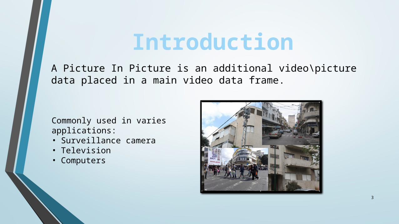
IntroductionA Picture In Picture is an additional video\picture data placed in a main video data frame.
Commonly used in varies applications:• Surveillance camera• Television• Computers
4
• “Smart” Algorithm – Picture In Picture
• Implementing a synthesizable solution with VHDL
• Using testing environment
Project Overview

5
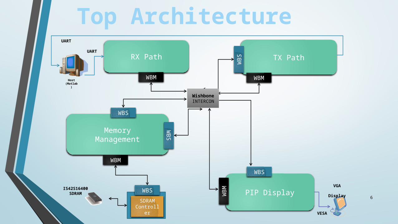
Requirements
• Internal communication via Wishbone protocol
• Input - External video (simulated as text)
• Output - Grayscale image resolution 800x600 pixels
• Main clock freq. 100MHz
• VESA (monitor) freq. 40 MHz
6
Top Architecture
PIP Display
WBS
VGA Display
WB
M
VESA
TX Path
MemoryManagement
RX Path
SDRAM Controller
WBS
WB
S
WBMWBM
WB
S
WBS
Host(Matlab
)
IS42S16400 SDRAM
WBM
UART
UART
WishboneINTERCON

7
PIP Display Block
Reg
VESA CONTROLLER
StateMachin
e
WBS
Clk Reset
FIFOWBM
WBM
WBM
40 MHz
100 MHz
dcFIFO
FIFO
FIFO
Sync
WBS
WBS
WBS
Small Frame1
Small Frame2
Large Frame
800 x 600

8
Micro Architecture – pin to pin
WBM FIFO
REGWBS
PIPDC FIFO
VESA
Sync

FIFO – Small 1
8 bit
FIFO – Small 2
FIFO – Background
x800
Small Frame 1
Small Frame 2
Background Frame
Micro Architecture – FIFO

10
FIFO – Small 1
FIFO – Background
Dc-FIFO

11
Micro Architecture PIP-SM
• 2 Counters (hcount, vcount)
• Default State – Large PIC
• Update from Reg – Start of Frame
• VSync – Changing Frames (x=800,y=600)

12
PIP State machineHDL view
State Machine – Using HDL
13
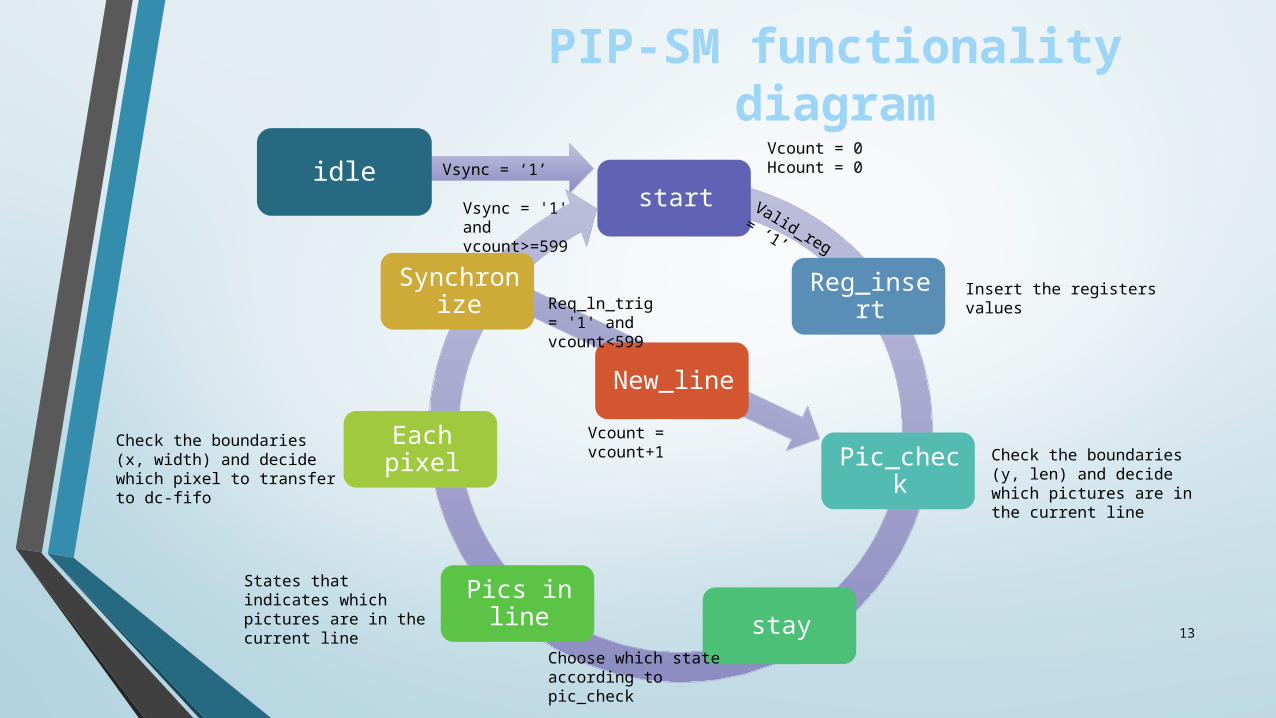
PIP-SM functionality diagram
start
Reg_insert
Pic_check
stayPics in
line
Each pixel
Synchronize
New_line
Vsync = ‘1’idleValid_reg =
‘1’
Check the boundaries (y, len) and decide which pictures are in the current line
Insert the registers values
Choose which state according to pic_check
States that indicates which pictures are in the current line
Check the boundaries (x, width) and decide which pixel to transfer to dc-fifo
Req_ln_trig = '1' and vcount<599
Vsync = '1' and vcount>=599
Vcount = vcount+1
Vcount = 0Hcount = 0

14
PIP-State machine
New_line
Small1_2
Small2_req
Small1_req
synchronize
Small1_2_small
2
Small1_2_small
1
Small1_2_b
ig
Small2_sm
all
Small2_b
ig
Small1_sm
all
Small1_b
ig
Pic_chec
k
stay
Big_pic
start
Reg_
insert
idle
Small1_2_writin
g
Small2_writi
ng
Small1_writin
g
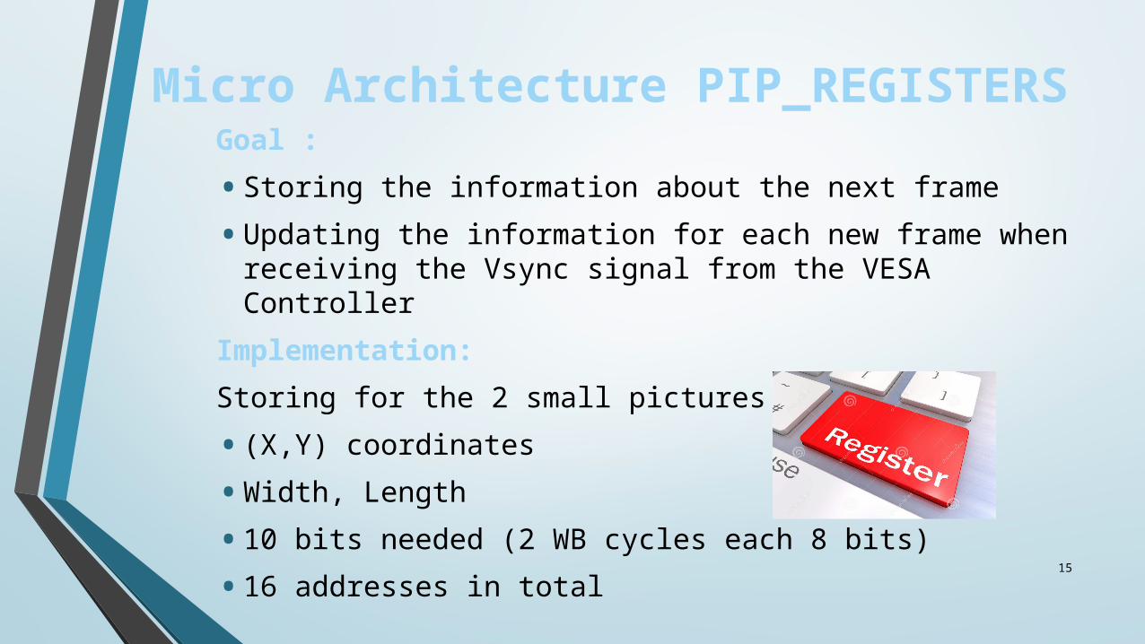
Micro Architecture PIP_REGISTERS
Goal :
• Storing the information about the next frame
• Updating the information for each new frame when receiving the Vsync signal from the VESA Controller
Implementation:
Storing for the 2 small pictures :
• (X,Y) coordinates
• Width, Length
• 10 bits needed (2 WB cycles each 8 bits)
• 16 addresses in total 15

16
Testing
• Dividing the components into testing groups by their functionality
• Testing the components as “stand alone” and groups of components by using TB
• Testing the “input group”, “output group” and the entire project, by using a testing environment.
17
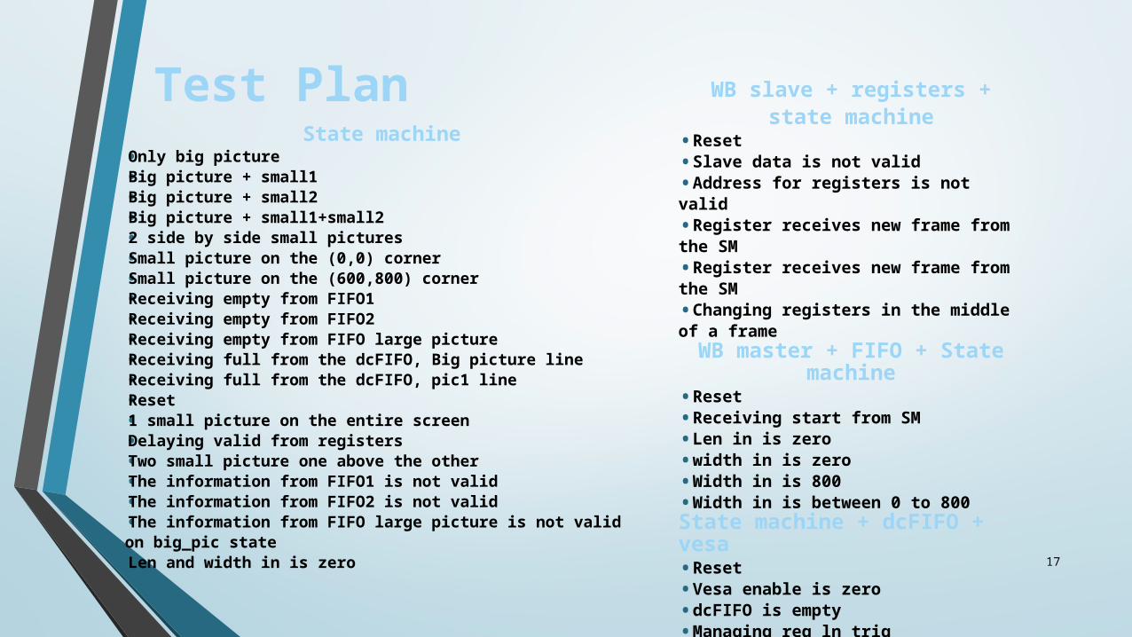
Test PlanState machine
•Only big picture •Big picture + small1•Big picture + small2•Big picture + small1+small2•2 side by side small pictures•Small picture on the (0,0) corner•Small picture on the (600,800) corner•Receiving empty from FIFO1 •Receiving empty from FIFO2•Receiving empty from FIFO large picture•Receiving full from the dcFIFO, Big picture line•Receiving full from the dcFIFO, pic1 line•Reset•1 small picture on the entire screen•Delaying valid from registers•Two small picture one above the other•The information from FIFO1 is not valid•The information from FIFO2 is not valid•The information from FIFO large picture is not valid on big_pic state•Len and width in is zero
WB slave + registers + state machine
•Reset•Slave data is not valid•Address for registers is not valid•Register receives new frame from the SM•Register receives new frame from the SM•Changing registers in the middle of a frame
WB master + FIFO + State machine
•Reset•Receiving start from SM•Len in is zero•width in is zero•Width in is 800•Width in is between 0 to 800State machine + dcFIFO + vesa•Reset•Vesa enable is zero•dcFIFO is empty•Managing req_ln_trig•Managing Vsync•Delayed write enable to dcFIFO•Changing the frame while broadcasting

18
PIP project•Reset•Only big picture •Big picture + small1•Big picture + small2•Big picture + small1+small2•2 side by side small pictures•Small picture on the (0,0) corner•Small picture on the (600,800) corner•1 small picture on the entire screen•Two small picture one above the other•Slave data is not valid•Address for registers is not valid•Valid from registers is Delayed•Len in of one of the small pictures is zero•width in of one of the small pictures is 800•Vesa enable is zero
Test Plan
19
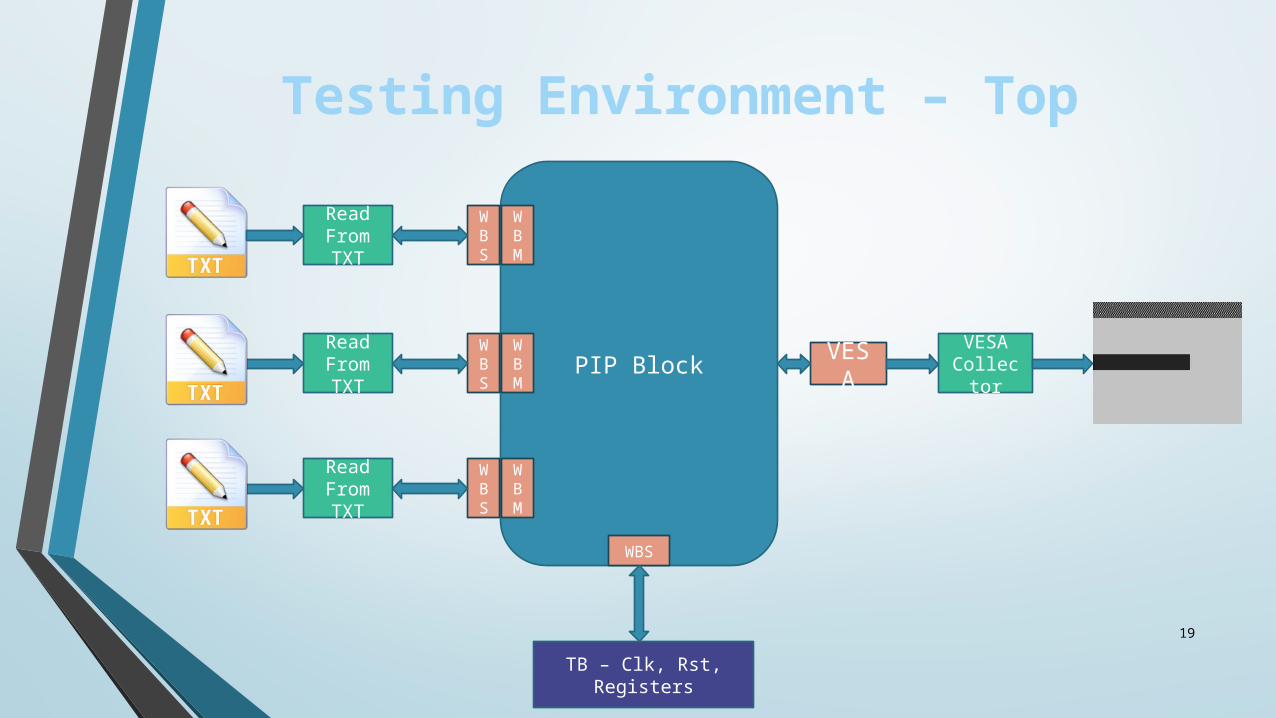
Testing Environment – Top
PIP Block
WBS
Read From TXT
WBM
VESA
VESA Collect
or
WBS
Read From TXT
WBM
WBS
Read From TXT
WBM
WBS
TB – Clk, Rst, Registers

20
Wave Forms Small to Big picture

21
Wave Forms Vsync Changes
22
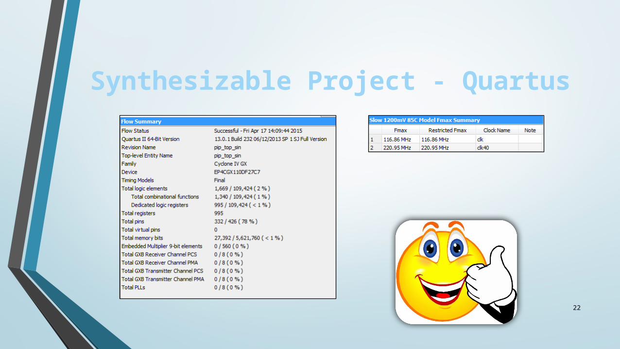
Synthesizable Project - Quartus

Problems & Solutions
Problem 1:
Working with 2 different frequencies
23
Solution:Storing the information targeted to the VESA Collector – DC FIFOSending feedback from VESA Collector to State Machine – 2FF Synchronizer

Problem 2:
Simulating communication entry by using only WB Master
24
Solution:Adding WB Slave as described in the final design , by that simplifying the video entry communication.
Solution:Not only checking if DC FIFO is full, but also checking if there is one or two spots left in the DC FIFO.
Problem 3:
Timing issues after connecting the State Machine to the DC FIFO

Problem 4:
Appearance of latches in the Quartus synthesis report.
25
Solution:Checking which signals created the latches and changing the signals characteristics from asynchronous signals to synchronous signals.
Solution:Adding 3 new writing states to the state machine and changing transitions and functionality of some of the states.
Problem 5:
Timing functionality problem of the PIP Block, caused by changing two signals from asynchronous to synchronous signals.
26
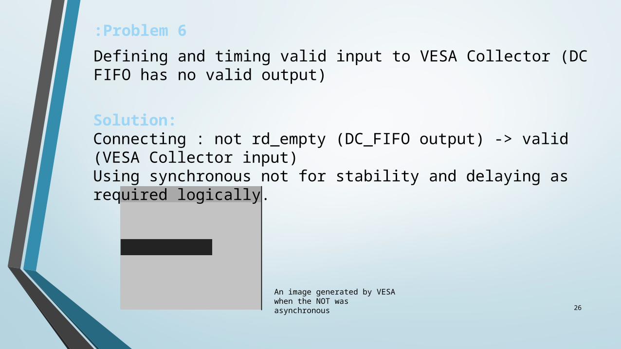
Problem 6:
Defining and timing valid input to VESA Collector (DC FIFO has no valid output)
An image generated by VESA when the NOT was asynchronous
Solution:Connecting : not rd_empty (DC_FIFO output) -> valid (VESA Collector input) Using synchronous not for stability and delaying as required logically.
What have we learned so far?
• Planning and Specifying a project
• Writing reusable, generic and synthesizable code
• Integration of many components
• Verify logic correctness using
waveforms, text files.
• Documentation of the work done