Polyphase Multifunction Energy Metering IC Data Sheet ...
96
Polyphase Multifunction Energy Metering IC Data Sheet ADE7854A/ADE7858A/ADE7868A/ADE7878A Rev. D Document Feedback Information furnished by Analog Devices is believed to be accurate and reliable. However, no responsibility is assumed by Analog Devices for its use, nor for any infringements of patents or other rights of third parties that may result from its use. Specifications subject to change without notice. No license is granted by implication or otherwise under any patent or patent rights of Analog Devices. Trademarks and registered trademarks are the property of their respective owners. One Technology Way, P.O. Box 9106, Norwood, MA 02062-9106, U.S.A. Tel: 781.329.4700 ©2020–2021 Analog Devices, Inc. All rights reserved. Technical Support www.analog.com FEATURES Highly accurate; supports EN 50470-1, EN 50470-3, IEC 62053-21, IEC 62053-22, and IEC 62053-23 standards Compatible with 3-phase, 3- or 4-wire (delta or wye) meters, and other 3-phase services Supplies total (fundamental and harmonic) active, reactive, and apparent energy and fundamental active/reactive energy on each phase and on the overall system 0.1% error (typical) in active and reactive energy over a dynamic range of 1000 to 1 at TA = 25°C 0.2% error (typical) in active and reactive energy over a dynamic range of 3000 to 1 at TA = 25°C Averaged rms measurements available in low ripple rms registers Supports current transformer and di/dt current sensors Dedicated ADC channel for neutral current input Estimated neutral current measurement by calculating the rms of the sum of the phase currents in all 3 phases 0.1% error (typical) in voltage and current rms over a dynamic range of 1000 to 1 at TA = 25°C Supplies sampled waveform data on all 3 phases and on neutral current Selectable no load thresholds for total and fundamental active and reactive powers, as well as for apparent powers Highly accurate low power battery mode phase current monitoring for antitampering detection Battery supply input for missing neutral operation Phase angle measurements in current and voltage channels Calibration frequency (CF) output directly drives LED and opto-isolators Reference: 1.2 V (drift of ±5 ppm/°C typical) with external overdrive capability Single 3.3 V supply 40-lead, Pb-free lead frame chip scale package (LFCSP) Operating temperature: −40°C to +85°C Flexible I 2 C, SPI, and HSDC serial interfaces GENERAL DESCRIPTION The ADE7854A/ADE7858A/ADE7868A/ADE7878A are high accuracy, 3-phase electrical energy measurement ICs with serial interfaces and three flexible pulse outputs. The devices incorporate second-order Σ-Δ analog-to-digital converters (ADCs), a digital integrator, reference circuitry, and all signal processing required to perform total (fundamental and harmonic) active, reactive (ADE7858A, ADE7868A, and ADE7878A), and apparent energy measurement and rms calculations. The ADE7878A can also perform fundamental-only active and reactive energy measurement and rms calculations. A fixed function digital signal processor (DSP) executes the signal processing. The DSP program is stored in the internal ROM memory. The ADE7854A/ADE7858A/ADE7868A/ADE7878A can measure active, reactive, and apparent energy in various 3-phase configurations, such as wye or delta services, with both three and four wires. Aside from regular rms measurements, which are updated every 8 kHz, these devices measure low ripple rms values, which are averaged internally and updated every 1.024 sec. The devices provide system calibration features for each phase, that is, rms offset correction, phase calibration, and gain calibration. The CF1, CF2, and CF3 logic outputs provide a wide selection of power information. All four devices provide total active and apparent powers, as well as the sum of the current rms values; the ADE7858A, ADE7868A, and ADE7878A also provide total reactive powers; whereas the ADE7878A provides fundamental active and reactive powers. The ADE7854A/ADE7858A/ADE7868A/ADE7878A contain waveform sampling registers that allow access to all ADC outputs. The devices also incorporate power quality measurements, such as short duration low or high voltage detection, short duration high current variation, line voltage period measurement, and angles between phase voltages and currents. Two serial interfaces, serial peripheral interface (SPI) and I 2 C, can communicate with the devices. A dedicated high speed interface, the high speed data capture (HSDC) port, can be used in conjunction with I 2 C to provide access to the ADC outputs and real-time power information. The devices have two interrupt request pins, IRQ0 and IRQ1 , to indicate that an enabled interrupt event has occurred. For the ADE7868A/ADE7878A, three specially designed low power modes ensure the continuity of energy accumulation when the ADE7868A/ADE7878A are in a tampering situation. Table 1 lists each device and its functions. These devices are available in 40-lead, Pb-free LFCSP packages. Table 1. Device Comparison Part No. WATT VAR I RMS, V RMS, and VA di/dt Fundamental WATT and VAR Tamper Detect and Low Power Modes ADE7854A Yes No Yes Yes No No ADE7858A Yes Yes Yes Yes No No ADE7868A Yes Yes Yes Yes No Yes ADE7878A Yes Yes Yes Yes Yes Yes
Transcript of Polyphase Multifunction Energy Metering IC Data Sheet ...

Polyphase MultifunctionEnergy Metering IC
Data Sheet ADE7854AADE7858AADE7868AADE7878A
Rev D Document Feedback Information furnished by Analog Devices is believed to be accurate and reliable However no responsibility is assumed by Analog Devices for its use nor for any infringements of patents or other rights of third parties that may result from its use Specifications subject to change without notice No license is granted by implication or otherwise under any patent or patent rights of Analog Devices Trademarks and registered trademarks are the property of their respective owners
One Technology Way PO Box 9106 Norwood MA 02062-9106 USATel 7813294700 copy2020ndash2021 Analog Devices Inc All rights reserved Technical Support wwwanalogcom
FEATURES Highly accurate supports EN 50470-1 EN 50470-3
IEC 62053-21 IEC 62053-22 and IEC 62053-23 standards Compatible with 3-phase 3- or 4-wire (delta or wye) meters
and other 3-phase services Supplies total (fundamental and harmonic) active reactive
and apparent energy and fundamental activereactive energy on each phase and on the overall system
01 error (typical) in active and reactive energy over a dynamic range of 1000 to 1 at TA = 25degC
02 error (typical) in active and reactive energy over a dynamic range of 3000 to 1 at TA = 25degC
Averaged rms measurements available in low ripple rms registers
Supports current transformer and didt current sensors Dedicated ADC channel for neutral current input Estimated neutral current measurement by calculating the
rms of the sum of the phase currents in all 3 phases 01 error (typical) in voltage and current rms over a
dynamic range of 1000 to 1 at TA = 25degC Supplies sampled waveform data on all 3 phases and on
neutral current Selectable no load thresholds for total and fundamental
active and reactive powers as well as for apparent powers Highly accurate low power battery mode phase current
monitoring for antitampering detection Battery supply input for missing neutral operation Phase angle measurements in current and voltage channels Calibration frequency (CF) output directly drives LED and
opto-isolators Reference 12 V (drift of plusmn5 ppmdegC typical) with external
overdrive capability Single 33 V supply 40-lead Pb-free lead frame chip scale package (LFCSP) Operating temperature minus40degC to +85degC Flexible I2C SPI and HSDC serial interfaces
GENERAL DESCRIPTION The ADE7854AADE7858AADE7868AADE7878A are high accuracy 3-phase electrical energy measurement ICs with serial interfaces and three flexible pulse outputs The devices incorporate second-order Σ-Δ analog-to-digital converters (ADCs) a digital integrator reference circuitry and all signal processing required to perform total (fundamental and harmonic) active reactive (ADE7858A ADE7868A and ADE7878A) and apparent energy measurement and rms calculations
The ADE7878A can also perform fundamental-only active and reactive energy measurement and rms calculations A fixed function digital signal processor (DSP) executes the signal processing The DSP program is stored in the internal ROM memory
The ADE7854AADE7858AADE7868AADE7878A can measure active reactive and apparent energy in various 3-phase configurations such as wye or delta services with both three and four wires Aside from regular rms measurements which are updated every 8 kHz these devices measure low ripple rms values which are averaged internally and updated every 1024 sec The devices provide system calibration features for each phase that is rms offset correction phase calibration and gain calibration
The CF1 CF2 and CF3 logic outputs provide a wide selection of power information All four devices provide total active and apparent powers as well as the sum of the current rms values the ADE7858A ADE7868A and ADE7878A also provide total reactive powers whereas the ADE7878A provides fundamental active and reactive powers
The ADE7854AADE7858AADE7868AADE7878A contain waveform sampling registers that allow access to all ADC outputs The devices also incorporate power quality measurements such as short duration low or high voltage detection short duration high current variation line voltage period measurement and angles between phase voltages and currents
Two serial interfaces serial peripheral interface (SPI) and I2C can communicate with the devices A dedicated high speed interface the high speed data capture (HSDC) port can be used in conjunction with I2C to provide access to the ADC outputs and real-time power information
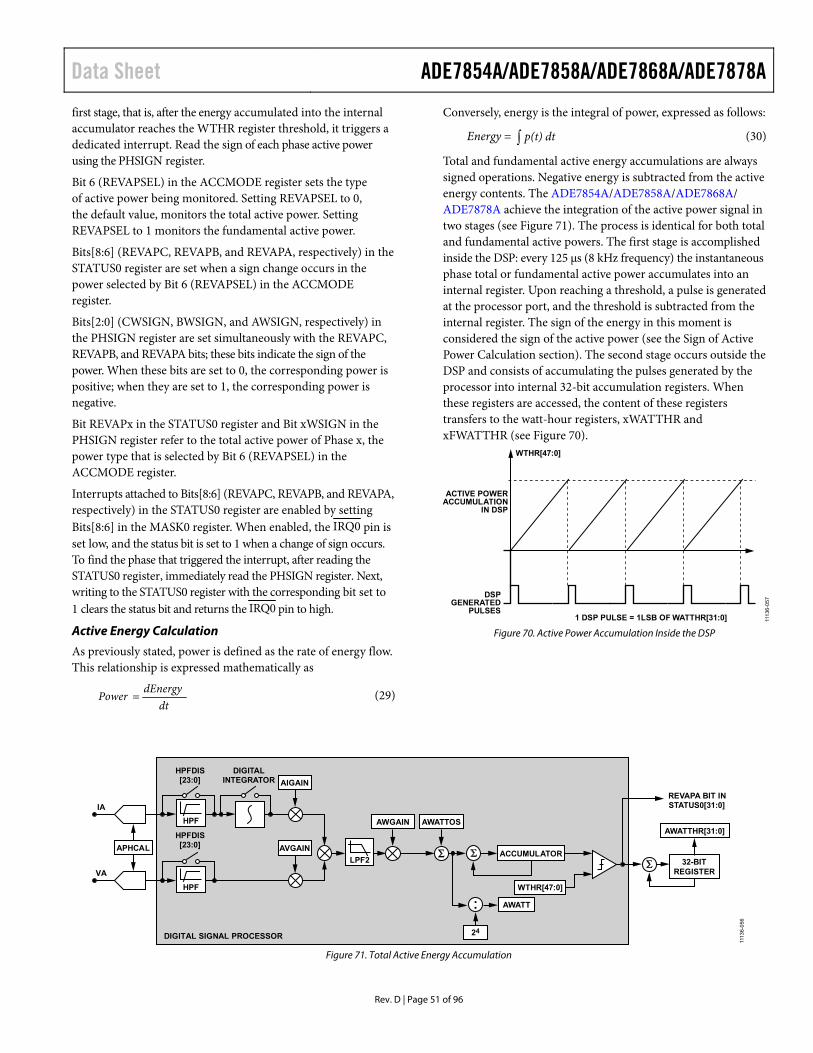
The devices have two interrupt request pins IRQ0 and IRQ1 to indicate that an enabled interrupt event has occurred For the ADE7868AADE7878A three specially designed low power modes ensure the continuity of energy accumulation when the ADE7868AADE7878A are in a tampering situation
Table 1 lists each device and its functions These devices are available in 40-lead Pb-free LFCSP packages
Table 1 Device Comparison
Part No WATT VAR
I RMS V RMS and VA didt
Fundamental WATT and VAR
Tamper Detect and Low Power Modes
ADE7854A Yes No Yes Yes No No ADE7858A Yes Yes Yes Yes No No ADE7868A Yes Yes Yes Yes No Yes ADE7878A Yes Yes Yes Yes Yes Yes
ADE7854AADE7858AADE7868AADE7878A Data Sheet
Rev D | Page 2 of 96
TABLE OF CONTENTS Features 1 General Description 1 Revision History 3 Functional Block Diagrams 4 Specifications 8
Timing Characteristics 11 Absolute Maximum Ratings 14
Thermal Resistance 14 ESD Caution 14
Pin Configuration and Function Descriptions 15 Typical Performance Characteristics 17 Test Circuit 20 Terminology 21 Power Management 22
PSM0 Normal Power Mode (All Devices) 22 PSM1 Reduced Power Mode (ADE7868A and ADE7878A Only) 22 PSM2 Low Power Mode (ADE7868A and ADE7878A Only) 22 PSM3 Sleep Mode (All Devices) 24 Power-Up Procedure 26 Hardware Reset 26 Software Reset 27
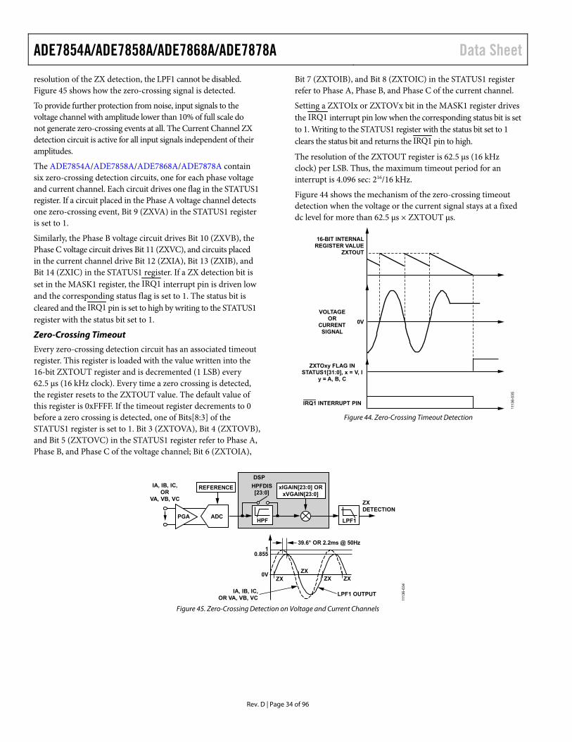
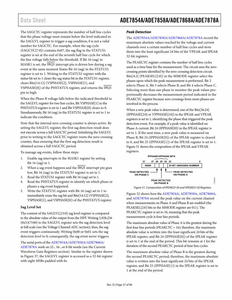
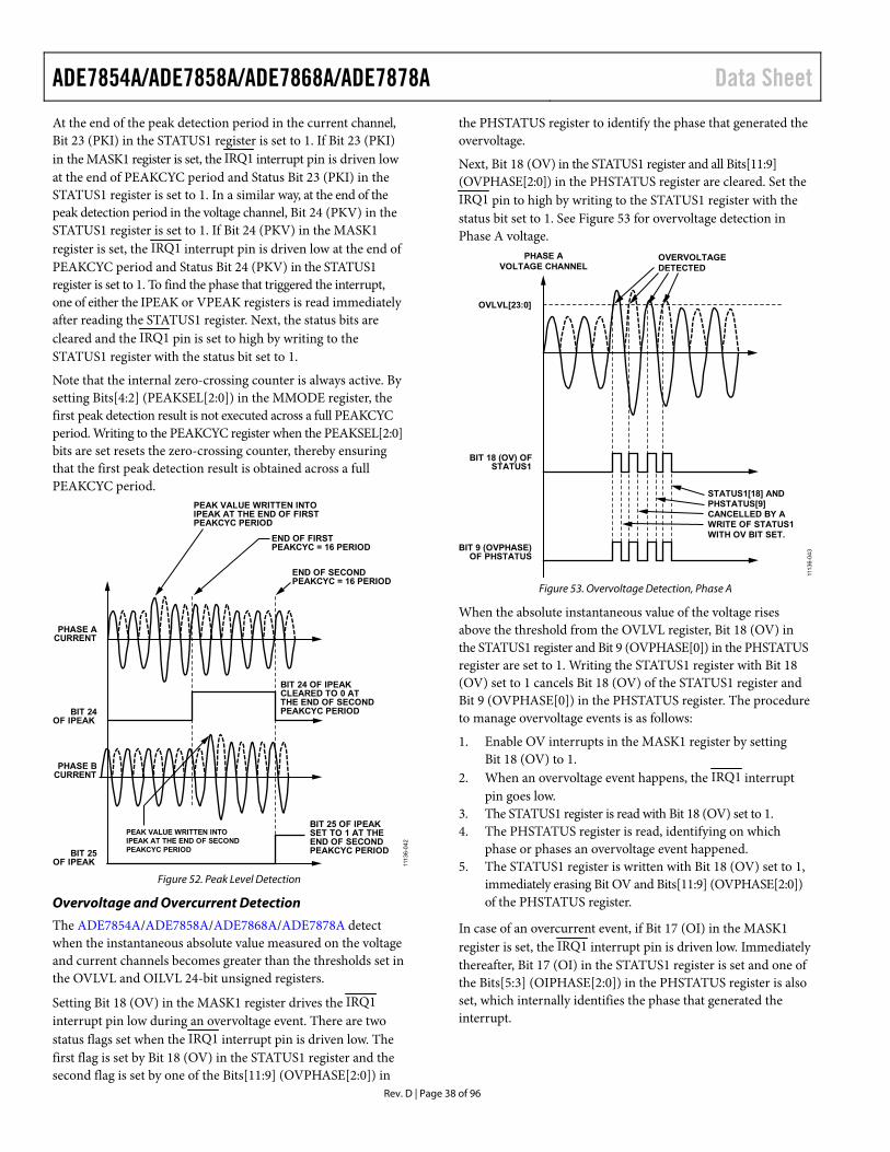
Theory of Operation 28 Analog Inputs 28 Analog-to-Digital Conversion 28 Current Channel ADC 29 didt Current Sensor and Digital Integrator 31 Voltage Channel ADC 32 Changing the Phase Voltage Datapath 33 Power Quality Measurements 33 Phase Compensation 41
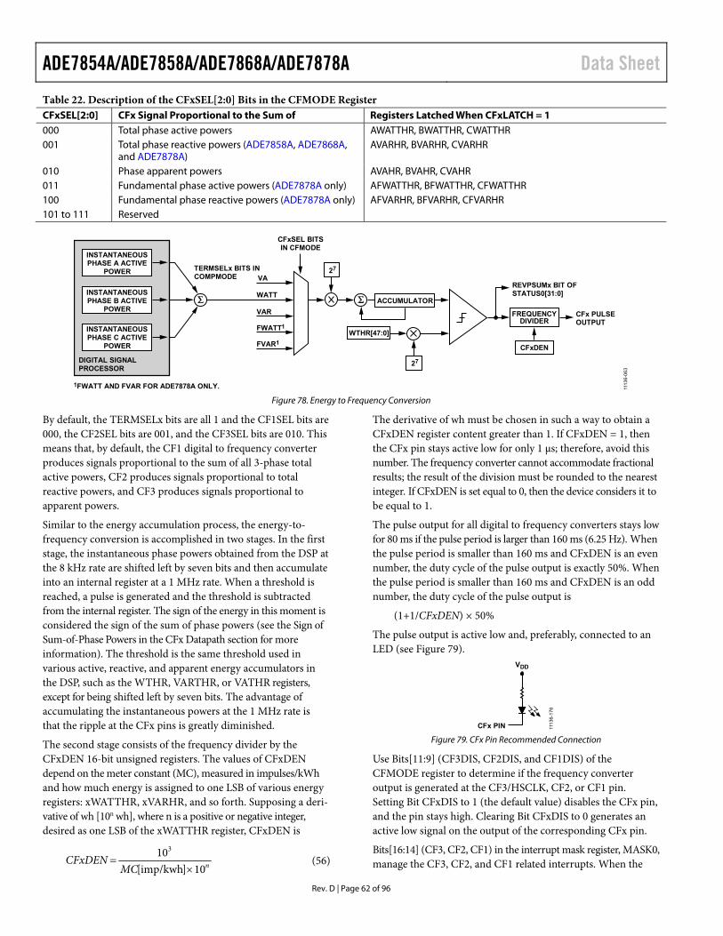
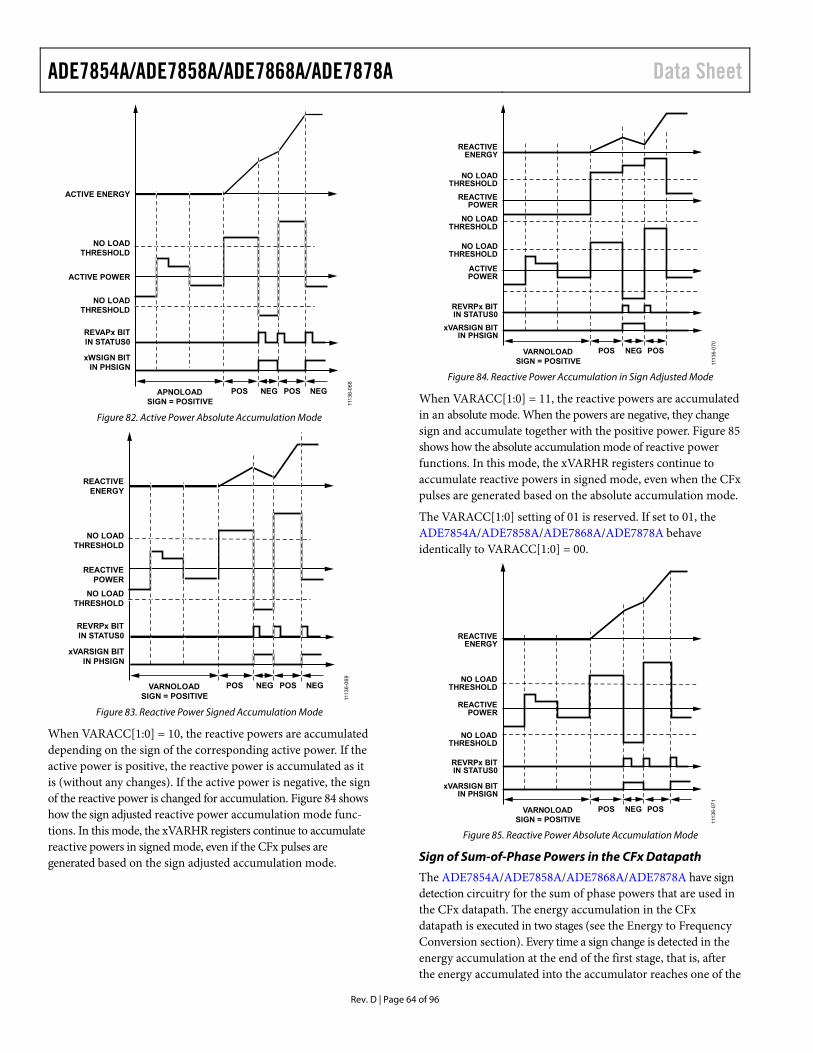
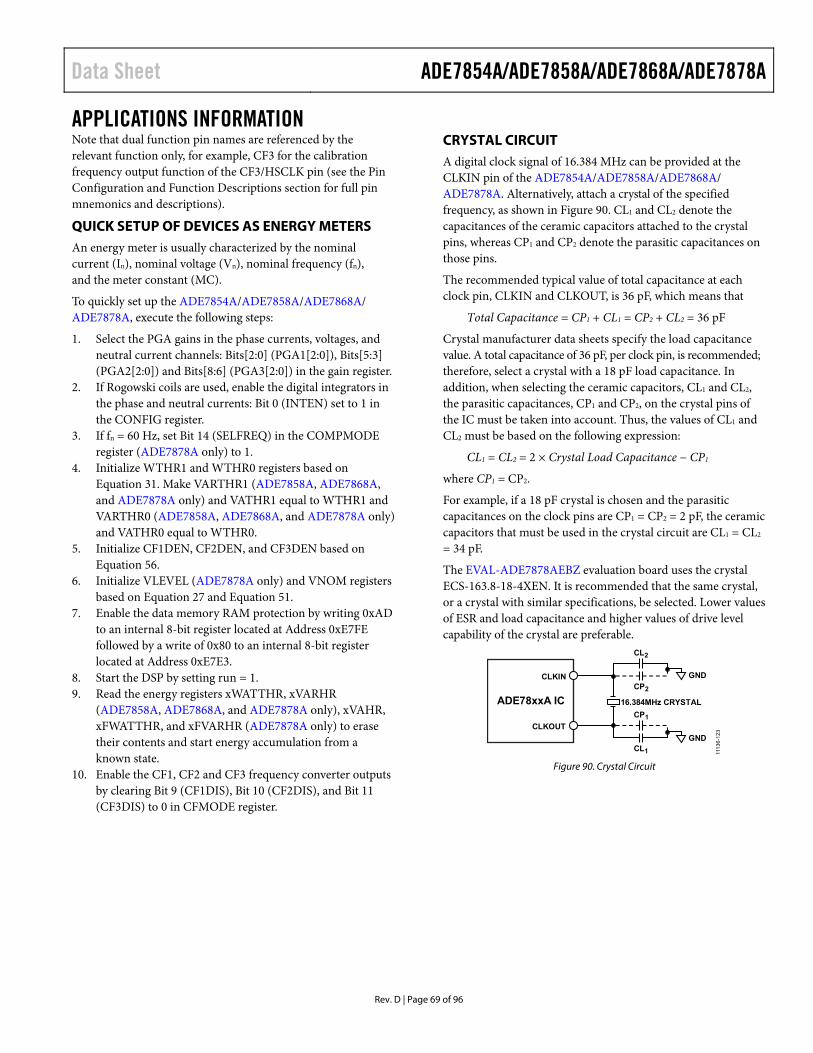
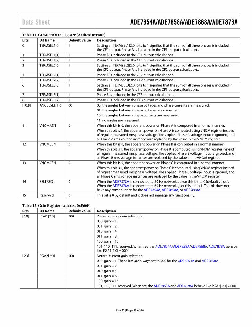
Reference Circuit 42 Digital Signal Processor 43 Root Mean Square Measurement 44 Active Power Calculation 48 Reactive Power CalculationmdashADE7858A ADE7868A ADE7878A Only 54 Apparent Power Calculation 58 Waveform Sampling Mode 61 Energy to Frequency Conversion 61 No Load Condition 65 Checksum Register 66 Interrupts 67
Applications Information 69 Quick Setup of Devices as Energy Meters 69 Crystal Circuit 69 Layout Guidelines 70 ADE7878A Evaluation Board 70 Die Version 70
Silicon Anomaly 71 ADE7854AADE7858AADE7868AADE7878A Functionality Issues 71 Functionality Issues 71
Serial Interfaces 72 Serial Interface Selection 72 Communication Verification 72 I2C-Compatible Interface 72 SPI-Compatible Interface 74 HSDC Interface 76
Register List 78 Outline Dimensions 96
Ordering Guide 96
Data Sheet ADE7854AADE7858AADE7868AADE7878A
Rev D | Page 3 of 96
REVISION HISTORY 32021mdashRev C to Rev D Changes to Figure 23 20 Changes to Neutral Current MismatchmdashADE7868A and ADE7878A Section 39 Changes to Figure 91 70 Added Table 25 Renumbered Sequentially 71 Changes to Section 1 Table 71 Updated Outline Dimensions 96 Changes to Ordering Guide 96
52016mdashRev B to Rev C Changes to ADE7854AADE7858AADE7868AADE7878A Functionality Issues Section Chip Marking Column 70 102014mdashRev A to Rev B Changes to Figure 23 19 Changes to Figure 27 25 Changes to Silicon Anomaly Section 70 72014mdashRevision A Initial Version
ADE7854AADE7858AADE7868AADE7878A Data Sheet
Rev D | Page 4 of 96
FUNCTIONAL BLOCK DIAGRAMS
PG
A1
PG
A1
PG
A1
PG
A3
PG
A3
PG
A3
12V
RE
F
DIG
ITA
L S
IGN
AL
PR
OC
ES
SO
R
AP
HC
AL
HP
FD
IS[2
30]
HP
F
HP
FD
IS[2
30]
DIG
ITA
LIN
TE
GR
AT
OR
HP
F
PO
RL
DO
LD
O
X2
AIR
MS
LP
F
AIR
MS
OS
X2
AV
RM
S yt
= 1
024
sec
LP
F
LP
F
AV
RM
SO
S
AV
AG
AIN
IAR
MS
_LR
IP
VA
RM
S_L
RIP
AW
GA
IND
FC
CF
1DE
N
DF
C
CF
2DE
N
DF
C
CF
3DE
N
524
2625
174
7 8 9 2212 13 14 19 18
3937383632293534333227 28 23
6
SP
IO
RI2
CH
SD
C
RE
SE
TR
EF
INO
UT
VD
DA
GN
DA
VD
DD
VD
DD
GN
D
CL
KIN
CL
KO
UT
IAP
IAN
VA
P
IBP
IBN
VB
P
ICP
ICN
VC
P
VN
PM
0
PM
1
CF
1
CF
2
CF
3H
SC
LK
IRQ
0
IRQ
1
SC
LK
SC
L
MO
SI
SD
A
MIS
OH
SD
SS
HS
A
20
RE
F_G
ND
AD
E7
85
4A
AD
C
AD
C
AD
C
AD
C
AD
C
AD
C
TO
TA
L A
CT
IVE
AP
PA
RE
NT
EN
ER
GIE
S A
ND
VO
LT
AG
E
CU
RR
EN
T R
MS
CA
LC
UL
AT
ION
FO
RP
HA
SE
C(S
EE
PH
AS
E A
FO
R D
ET
AIL
ED
DA
TA
PA
TH
)
TO
TA
L A
CT
IVE
AP
PA
RE
NT
EN
ER
GIE
S A
ND
VO
LT
AG
E
CU
RR
EN
T R
MS
CA
LC
UL
AT
ION
FO
RP
HA
SE
B(S
EE
PH
AS
E A
FO
R D
ET
AIL
ED
DA
TA
PA
TH
)
PH
AS
E A
P
HA
SE
B
AN
DP
HA
SE
CD
AT
A
AW
AT
TO
S
AV
GA
IN
AIG
AIN
11136-001
yxx
t =
10
24 s
ec
Figure 1 ADE7854A Functional Block Diagram
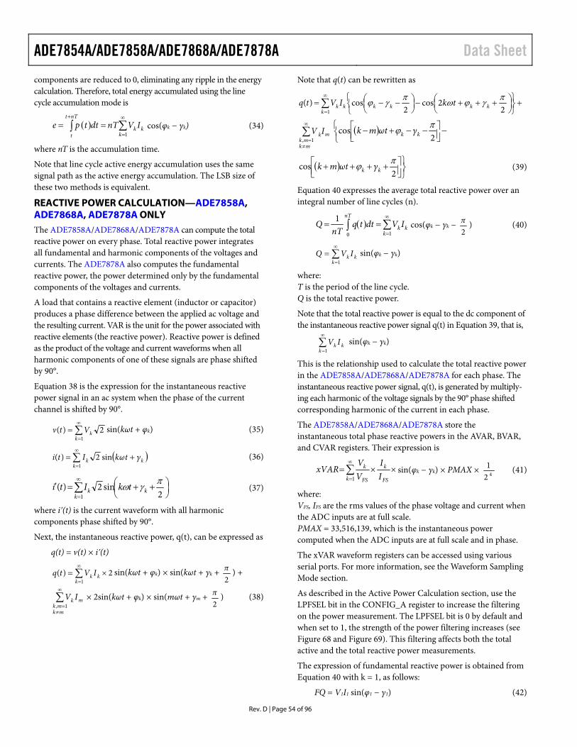
Data Sheet ADE7854AADE7858AADE7868AADE7878A
Rev D | Page 5 of 96
PG
A1
PG
A1
PG
A1
PG
A3
PG
A3
PG
A3
12V
RE
F
DIG
ITA
L S
IGN
AL
PR
OC
ES
SO
R
CO
MP
UT
AT
ION
AL
BL
OC
K F
OR
TO
TA
LR
EA
CT
IVE
PO
WE
R
AP
HC
AL
PO
RL
DO
LD
O
X2
AIR
MS
LP
F
AIR
MS
OS
X2
AV
RM
SL
PF
LP
F
AV
RM
SO
S
AV
AG
AIN
AVA
RG
AIN
AVA
RO
S
DF
C
CF
1DE
N
DF
C
CF
2DE
N
DF
C
CF
3DE
N
524
26
2517
4
7 8 9 2212 13 14 19 18
3937383632293534333227 28 23
6
RE
SE
TR
EF
INO
UT
VD
DA
GN
DA
VD
DD
VD
DD
GN
D
CL
KIN
CL
KO
UT
IAP
IAN
VA
P
IBP
IBN
VB
P
ICP
ICN
VC
P
VN
PM
0
PM
1
CF
1
CF
2
CF
3H
SC
LK
IRQ
0
IRQ
1
SC
LK
SC
L
MO
SI
SD
A
MIS
OH
SD
SS
HS
A
AD
E7
85
8A
AD
C
AD
C
AD
C
AD
C
AD
C
AD
C
TO
TA
L A
CT
IVE
RE
AC
TIV
E
AP
PA
RE
NT
EN
ER
GIE
S A
ND
VO
LT
AG
EC
UR
RE
NT
RM
S C
AL
CU
LA
TIO
N F
OR
PH
AS
E B
(SE
E P
HA
SE
A F
OR
DE
TA
ILE
DD
AT
AP
AT
H)
TO
TA
L A
CT
IVE
RE
AC
TIV
E
AP
PA
RE
NT
EN
ER
GIE
S A
ND
VO
LT
AG
EC
UR
RE
NT
RM
S C
AL
CU
LA
TIO
N F
OR
PH
AS
E C
(SE
E P
HA
SE
A F
OR
DE
TA
ILE
DD
AT
AP
AT
H)
PH
AS
E A
P
HA
SE
B
AN
DP
HA
SE
CD
AT
A
AW
GA
INA
WA
TT
OS
HP
F
HP
FD
IS[2
30]
HP
FD
IS[2
30]
DIG
ITA
LIN
TE
GR
AT
OR
HP
F
SP
IO
RI2
CH
SD
C
AV
GA
IN
AIG
AIN
11136-002
20
RE
F_G
ND
yt
= 1
024
sec
IAR
MS
_LR
IP
VA
RM
S_L
RIP
yxx
t =
10
24 s
ec
Figure 2 ADE7858A Functional Block Diagram
ADE7854AADE7858AADE7868AADE7878A Data Sheet
Rev D | Page 6 of 96
PG
A1
PG
A1
PG
A1
PG
A3
PG
A3
PG
A3
12V
RE
F
TO
TA
L A
CT
IVE
RE
AC
TIV
E
AP
PA
RE
NT
EN
ER
GIE
S A
ND
VO
LT
AG
EC
UR
RE
NT
RM
S C
AL
CU
LA
TIO
N F
OR
PH
AS
E B
(SE
E P
HA
SE
A F
OR
DE
TA
ILE
DD
AT
AP
AT
H)
TO
TA
L A
CT
IVE
RE
AC
TIV
E
AP
PA
RE
NT
EN
ER
GIE
S A
ND
VO
LT
AG
EC
UR
RE
NT
RM
S C
AL
CU
LA
TIO
N F
OR
PH
AS
E C
(SE
E P
HA
SE
A F
OR
DE
TA
ILE
DD
AT
AP
AT
H)
DIG
ITA
L S
IGN
AL
PR
OC
ES
SO
R
CO
MP
UT
AT
ION
AL
BL
OC
K F
OR
TO
TA
LR
EA
CT
IVE
PO
WE
R
AP
HC
AL
HP
FD
IS[2
30]
HP
F
HP
FD
IS[2
30]
HP
F
HP
FD
IS[2
30]
DIG
ITA
LIN
TE
GR
AT
OR
HP
F
DIG
ITA
LIN
TE
GR
AT
OR
PO
RL
DO
LD
O
X2
AIR
MS
LP
F
AIR
MS
OS
X2
X2
AV
RM
SL
PF
LP
F
AV
RM
SO
S
AV
AG
AIN
LP
F
AW
GA
IN
NIR
MS
NIR
MS
OS
AW
AT
TO
S
AV
AR
GA
INA
VA
RO
S
DF
C
CF
1DE
N
DF
C
CF
2DE
N
DF
C
CF
3DE
N
524
2625
174
7 8 9 2212 13 14 19 18
3937383632293534333227 28 23
6
RE
SE
TR
EF
INO
UT
VD
DA
GN
DA
VD
DD
VD
DD
GN
D
CL
KIN
CL
KO
UT
IAP
IAN
VA
P
IBP
IBN
VB
P
ICP
ICN
VC
P
VN
PM
0
PM
1
CF
1
CF
2
CF
3H
SC
LK
IRQ
0
IRQ
1
SC
LK
SC
L
MO
SI
SD
A
MIS
OH
SD
SS
HS
A
AD
E7
86
8A
AD
C
AD
C
AD
C
AD
C
AD
C
AD
C
PG
A2
15 16
INP
INN
AD
C
PH
AS
E A
P
HA
SE
B
AN
DP
HA
SE
CD
AT
A
SP
IO
RI2
CH
SD
C
NIG
AIN
AIG
AIN
AV
GA
IN
11136-003
20
RE
F_G
ND
yt
= 1
024
sec
IAR
MS
_LR
IP
VA
RM
S_L
RIP
yxx
t =
10
24 s
ec
INR
MS
x_L
RIP
zz
t =
10
24 s
ec
Figure 3 ADE7868A Functional Block Diagram
Data Sheet ADE7854AADE7858AADE7868AADE7878A
Rev D | Page 7 of 96
PG
A1
PG
A1
PG
A1
PG
A3
PG
A3
PG
A3
12V
RE
F
TO
TA
LF
UN
DA
ME
NT
AL
AC
TIV
E
RE
AC
TIV
E E
NE
RG
IES
A
PP
AR
EN
TE
NE
RG
Y A
ND
VO
LT
AG
EC
UR
RE
NT
RM
S C
AL
CU
LA
TIO
N F
OR
PH
AS
E B
(SE
E P
HA
SE
A F
OR
DE
TA
ILE
DD
AT
AP
AT
H)
TO
TA
LF
UN
DA
ME
NT
AL
AC
TIV
E
RE
AC
TIV
E E
NE
RG
IES
A
PP
AR
EN
TE
NE
RG
Y A
ND
VO
LT
AG
EC
UR
RE
NT
RM
S C
AL
CU
LA
TIO
N F
OR
PH
AS
E C
(SE
E P
HA
SE
A F
OR
DE
TA
ILE
DD
AT
AP
AT
H)
CO
MP
UT
AT
ION
AL
BL
OC
K F
OR
TO
TA
LR
EA
CT
IVE
PO
WE
R
AP
HC
AL
HP
FD
IS[2
30]
HP
F
HP
FD
IS[2
30]
HP
F
HP
FD
IS[2
30]
DIG
ITA
LIN
TE
GR
AT
OR
HP
F
DIG
ITA
LIN
TE
GR
AT
OR
PO
RL
DO
LD
O
X2
AIR
MS
LP
F
AIR
MS
OS
X2
X2
AV
RM
SL
PF
LP
F
AV
RM
SO
S
AV
AG
AIN
LP
F
CO
MP
UT
AT
ION
AL
BL
OC
K F
OR
FU
ND
AM
EN
TA
LA
CT
IVE
AN
DR
EA
CT
IVE
PO
WE
R
AW
GA
IN
NIR
MS
NIR
MS
OS
AW
AT
TO
S
AV
AR
GA
INA
VA
RO
S
AF
WG
AIN
AF
WA
TT
OS
AF
VA
RG
AIN
AF
VA
RO
S
PH
AS
E A
P
HA
SE
B
AN
DP
HA
SE
CD
AT
A
DF
C
CF
1DE
N
DF
C
CF
2DE
N
DF
C
CF
3DE
N
524
26
2517
4
7 8 9 2212 13 14 19 18
3937383632293534333227 28 23
6
RE
SE
TR
EF
INO
UT
VD
DA
GN
DA
VD
DD
VD
DD
GN
D
CL
KIN
CL
KO
UT
IAP
IAN
VA
P
IBP
IBN
VB
P
ICP
ICN
VC
P
VN
PM
0
PM
1
CF
1
CF
2
CF
3H
SC
LK
IRQ
0
IRQ
1
SC
LK
SC
L
MO
SI
SD
A
MIS
OH
SD
SS
HS
A
AD
E7
87
8A
AD
C
AD
C
AD
C
AD
C
AD
C
AD
C
PG
A2
15 16
INP
INN
AD
C
SP
IO
RI2
CH
SD
C
AV
GA
IN
NIG
AIN
AIG
AIN
11136-004
20
RE
F_G
ND
yt
= 1
024
sec
IAR
MS
_LR
IP
VA
RM
S_L
RIP
yxx
t =
10
24 s
ec D
IGIT
AL
SIG
NA
LP
RO
CE
SS
OR
INR
MS
x_L
RIP
zz
t =
10
24 s
ec
Figure 4 ADE7878A Functional Block Diagram
ADE7854AADE7858AADE7868AADE7878A Data Sheet
Rev D | Page 8 of 96
SPECIFICATIONS VDD = 33 V plusmn 10 AGND = DGND = 0 V on-chip reference CLKIN = 16384 MHz TMIN to TMAX = minus40degC to +85degC TTYP = 25degC unless otherwise noted
Table 2 Parameter1 2 3 Min Typ Max Unit Test ConditionsComments ACTIVE ENERGY MEASUREMENT (PSM0 MODE)
Active Energy Measurement Error (Per Phase) Total Active Energy 01 Over a dynamic range of 1000 to 1
PGA = 1 2 4 integrator off 02 Over a dynamic range of 3000 to 1
PGA = 1 2 4 integrator off 01 Over a dynamic range of 500 to 1
PGA = 8 16 integrator on Fundamental Active Energy ADE7878A only 01 Over a dynamic range of 1000 to 1
PGA = 1 2 4 integrator off 02 Over a dynamic range of 3000 to 1
PGA = 1 2 4 integrator off 01 Over a dynamic range of 500 to 1
PGA = 8 16 integrator on AC Power Supply Rejection VDD = 33 V + 120 mV rms at 120 Hz100 Hz
IxP = VxP = plusmn100 mV rms Output Frequency Variation 001
DC Power Supply Rejection VDD = 33 V plusmn 330 mV dc IxP = VxP = plusmn100 mV rms
Output Frequency Variation 001 Total Active Energy Measurement Bandwidth 2 kHz
REACTIVE ENERGY MEASUREMENT (PSM0 MODE) ADE7858A ADE7868A and ADE7878A Reactive Energy Measurement Error (Per Phase)
Total Reactive Energy 01 Over a dynamic range of 1000 to 1 PGA = 1 2 4 integrator off
02 Over a dynamic range of 3000 to 1 PGA = 1 2 4 integrator off
01 Over a dynamic range of 500 to 1 PGA = 8 16 integrator on
Fundamental Reactive Energy ADE7878A only 01 Over a dynamic range of 1000 to 1
PGA = 1 2 4 integrator off 02 Over a dynamic range of 3000 to 1
PGA = 1 2 4 integrator off 01 Over a dynamic range of 500 to 1
PGA = 8 16 integrator on AC Power Supply Rejection VDD = 33 V + 120 mV rms at 120 Hz100 Hz
IxP = VxP = plusmn100 mV rms Output Frequency Variation 001
DC Power Supply Rejection VDD = 33 V plusmn 330 mV dc IxP = VxP = plusmn100 mV rms
Output Frequency Variation 001 Total Reactive Energy Measurement Bandwidth 2 kHz
RMS MEASUREMENTS (PSM0 MODE) Current (I) RMS and Voltage (V) RMS
Measurement Bandwidth 2 kHz
I RMS and V RMS Measurement Error 01 Over a dynamic range of 1000 to 1 PGA = 1
MEAN ABSOLUTE VALUE (MAV) MEASUREMENT (PSM1 Mode)
ADE7868A and ADE7878A
I MAV Measurement Bandwidth 260 Hz I MAV Measurement Error 05 Over a dynamic range of 100 to 1 PGA = 1 2
4 8
Data Sheet ADE7854AADE7858AADE7868AADE7878A
Rev D | Page 9 of 96
Parameter1 2 3 Min Typ Max Unit Test ConditionsComments ANALOG INPUTS
Maximum Signal Levels plusmn500 mV peak PGA = 1 differential or single-ended inputs between the following pins IAP and IAN IBP and IBN ICP and ICN INP and INN single-ended inputs between the following pins VAP and VN VBP and VN VCP and VN
Input Impedance (DC) IAP IAN IBP IBN ICP ICN INP INN VAP
VBP and VCP Pins 400 kΩ
VN Pin 130 kΩ ADC Offset minus34 mV PGA = 1 see the Terminology section Gain Error plusmn4 External 12 V reference
WAVEFORM SAMPLING Sampling CLKIN2048 16384 MHz2048 = 8 kSPS
Current and Voltage Channels See the Waveform Sampling Mode section Signal-to-Noise Ratio SNR 74 dB PGA = 1 fundamental frequency = 45 Hz to
65 Hz see the Terminology section Signal-to-Noise-and-Distortion (SINAD)
Ratio 74 dB PGA = 1 fundamental frequency = 45 Hz to
65 Hz see the Terminology section Bandwidth (minus3 dB) 2 kHz
TIME INTERVAL BETWEEN PHASES Measurement Error 03 Degrees Line frequency = 45 Hz to 65 Hz HPF on
CF1 CF2 CF3 PULSE OUTPUTS Maximum Output Frequency 8 kHz WTHR = VARTHR = VATHR = PMAX =
33516139 Duty Cycle 50 CF1 CF2 or CF3 frequency gt 625 Hz CFDEN
is even and gt 1 (1 + 1CFDEN)
times 50 CF1 CF2 or CF3 frequency gt 625 Hz CFDEN
is odd and gt 1 Active Low Pulse Width 80 ms CF1 CF2 or CF3 frequency lt 625 Hz Jitter 004 CF1 CF2 or CF3 frequency = 1 Hz nominal
phase currents larger than 10 of full scale
REFERENCE INPUT REFINOUT Input Voltage Range 11 13 V Minimum = 12 V minus 8 maximum = 12 V + 8 Input Capacitance 10 pF
ON-CHIP REFERENCE PSM0 AND PSM1 MODES Nominal 12 V at the REFINOUT pin at TA = 25degC Temperature Coefficient minus32 plusmn5 +32 ppmdegC Drift across the entire temperature range of
minus40degC to +85degC is calculated with reference to 25degC see the Reference Circuit section
CLKIN CLKIN = 16384 MHz see the Crystal Circuit section
Input Clock Frequency 1622 16384 1655 MHz
LOGIC INPUTSmdashMOSISDA SCLKSCL SSHSA RESET PM0 AND PM1
Input High Voltage VINH 20 V VDD = 33 V plusmn 10 Input Low Voltage VINL 08 V VDD = 33 V plusmn 10 Input Current IIN minus87 μA Input = 0 V VDD = 33 V
3 μA Input = VDD = 33 V Input Capacitance CIN 10 pF
LOGIC OUTPUTS IRQ0 IRQ1 MISOHSD
Output High Voltage VOH 24 V VDD = 33 V plusmn 10 ISOURCE 800 μA
Output Low Voltage VOL 04 V VDD = 33 V plusmn 10 ISINK 2 mA
ADE7854AADE7858AADE7868AADE7878A Data Sheet
Rev D | Page 10 of 96
Parameter1 2 3 Min Typ Max Unit Test ConditionsComments CF1 CF2 CF3HSCLK
Output High Voltage VOH 24 V VDD = 33 V plusmn 10 ISOURCE 500 μA
Output Low Voltage VOL 04 V VDD = 33 V plusmn 10 ISINK 8 mA
POWER SUPPLY For specified performance PSM0 Mode
VDD Pin 297 363 V Minimum = 33 V minus 10 maximum = 33 V + 10
IDD 20 23 mA PSM1 and PSM2 Modes ADE7868A and ADE7878A
VDD Pin 28 37 V IDD
PSM1 Mode 45 mA PSM2 Mode 02 mA
PSM3 Mode VDD Pin 28 37 V IDD 17 μA
1 See the Typical Performance Characteristics section 2 See the Terminology section for a definition of the parameters 3 Note that dual function pin names are referenced by the relevant function only (see the Pin Configuration and Function Descriptions section for full pin mnemonics
and descriptions)
Data Sheet ADE7854AADE7858AADE7868AADE7878A
Rev D | Page 11 of 96
TIMING CHARACTERISTICS VDD = 33 V plusmn 10 AGND = DGND = 0 V on-chip reference CLKIN = 16384 MHz TMIN to TMAX = minus40degC to +85degC Note that within the timing tables and diagrams dual function pin names are referenced by the relevant function only (see the Pin Configuration and Function Descriptions section for full pin mnemonics and descriptions)
I2C Interface Timing
Table 3 Standard Mode Fast Mode Parameter Symbol Min Max Min Max Unit SCL Clock Frequency fSCL 0 100 0 400 kHz Hold Time for Start and Repeated Start Conditions tHDSTA 40 06 μs Low Period of SCL Clock tLOW 47 13 μs High Period of SCL Clock tHIGH 40 06 μs Setup Time for Repeated Start Condition tSUSTA 47 06 μs Data Hold Time tHDDAT 0 345 0 09 μs Data Setup Time tSUDAT 250 100 ns Rise Time of SDA and SCL Signals tR 1000 20 300 ns Fall Time of SDA and SCL Signals tF 300 20 300 ns Setup Time for Stop Condition tSUSTO 40 06 μs Bus Free Time Between a Stop and Start Condition tBUF 47 13 μs Pulse Width of Suppressed Spikes tSP NA1 50 ns 1 NA means not applicable
tF
tR
tHDDAT
tHDSTA
tHIGHtSUSTA
tSUDAT
tF
tHDSTA tSP
tSUSTO
tRtBUF
tLOW
SDA
SCL
STARTCONDITION
REPEATED STARTCONDITION
STOPCONDITION
STARTCONDITION 11
13
6-0
05
Figure 5 I2C Interface Timing
ADE7854AADE7858AADE7868AADE7878A Data Sheet
Rev D | Page 12 of 96
SPI Interface Timing
Table 4 Parameter Symbol Min Max Unit SS to SCLK Edge tSS 50 ns
SCLK Period 04 40001 μs SCLK Low Pulse Width tSL 175 ns SCLK High Pulse Width tSH 175 ns Data Output Valid After SCLK Edge tDAV 100 ns Data Input Setup Time Before SCLK Edge tDSU 100 ns Data Input Hold Time After SCLK Edge tDHD 5 ns Data Output Fall Time tDF 20 ns Data Output Rise Time tDR 20 ns SCLK Rise Time tSR 20 ns SCLK Fall Time tSF 20 ns MISO Disable After SS Rising Edge tDIS 200 ns
SS High After SCLK Edge tSFS 0 ns 1 Guaranteed by design
MSB LSB
LSB IN
INTERMEDIATE BITS
INTERMEDIATE BITS
tSFS
tDIS
tSS
tSL
tDF
tSH
tDHD
tDAV
tDSU
tSRtSF
tDR
MSB INMOSI
MISO
SCLK
SS
111
36-
00
6
Figure 6 SPI Interface Timing
Data Sheet ADE7854AADE7858AADE7868AADE7878A
Rev D | Page 13 of 96
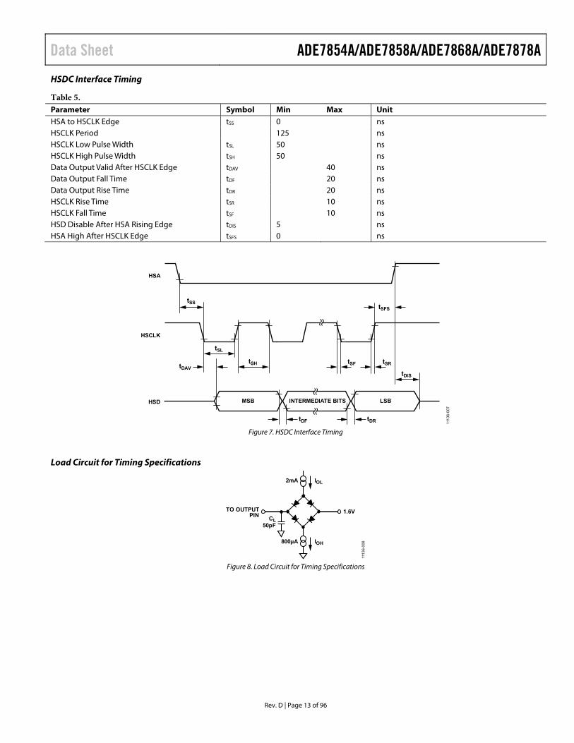
HSDC Interface Timing
Table 5 Parameter Symbol Min Max Unit HSA to HSCLK Edge tSS 0 ns HSCLK Period 125 ns HSCLK Low Pulse Width tSL 50 ns HSCLK High Pulse Width tSH 50 ns Data Output Valid After HSCLK Edge tDAV 40 ns Data Output Fall Time tDF 20 ns Data Output Rise Time tDR 20 ns HSCLK Rise Time tSR 10 ns HSCLK Fall Time tSF 10 ns HSD Disable After HSA Rising Edge tDIS 5 ns HSA High After HSCLK Edge tSFS 0 ns
MSB LSBINTERMEDIATE BITS
tSFS
tDIS
tSS
tSL
tDF
tSHtDAVtSRtSF
tDR
HSD
HSCLK
HSA
111
36-0
07
Figure 7 HSDC Interface Timing
Load Circuit for Timing Specifications
2mA IOL
800microA IOH
16VTO OUTPUTPIN
CL50pF
111
36
-00
8
Figure 8 Load Circuit for Timing Specifications
ADE7854AADE7858AADE7868AADE7878A Data Sheet
Rev D | Page 14 of 96
ABSOLUTE MAXIMUM RATINGS TA = 25degC unless otherwise noted
Table 6 Parameter Rating VDD to AGND minus03 V to +37 V VDD to DGND minus03 V to +37 V Analog Input Voltage to AGND IAP IAN
IBP IBN ICP ICN VAP VBP VCP VN minus2 V to +2 V
Analog Input Voltage to INP and INN minus2 V to +2 V Reference Input Voltage to AGND minus03 V to VDD + 03 V Digital Input Voltage to DGND minus03 V to VDD + 03 V Digital Output Voltage to DGND minus03 V to VDD + 03 V Operating Temperature
Industrial Range minus40degC to +85degC Storage Temperature Range minus65degC to +150degC
Lead Temperature (Soldering 10 sec) 300degC
Stresses at or above those listed under Absolute Maximum Ratings may cause permanent damage to the product This is a stress rating only functional operation of the product at these or any other conditions above those indicated in the operational section of this specification is not implied Operation beyond the maximum operating conditions for extended periods may affect product reliability
THERMAL RESISTANCE θJA is specified at 293degCW θJC is specified at 18degCW
Table 7 Thermal Resistance Package Type θJA θJC Unit 40-Lead LFCSP 293 18 degCW
ESD CAUTION
Data Sheet ADE7854AADE7858AADE7868AADE7878A
Rev D | Page 15 of 96
PIN CONFIGURATION AND FUNCTION DESCRIPTIONS
NOTES1 NC = NO CONNECT THESE PINS ARE NOT CONNECTED INTERNALLY IT IS RECOMMENDED THAT THESE PINS BE GROUNDED
2 CREATE A SIMILAR PAD ON THE PCB UNDER THE EXPOSED PAD SOLDER THE EXPOSED PAD TO THE PAD ON THE PCB TO CONFER MECHANICAL STRENGTH TO THE PACKAGE CONNECT THE PADS TO AGND AND DGND
11N
C12
IBN
13IC
P
15IN
P
17R
EF
INO
UT
16IN
N
18V
N19
VC
P20
RE
F_G
ND
14IC
N
NCPM0PM1
RESETDVDDDGND
IAPIANIBPNC
VAPAVDDAGNDVDDCLKINCLKOUTIRQ0NC
VBPNC
33C
F1
CF
235 34
CF
3H
SC
LK
36S
CL
KS
CL
37M
ISO
HS
D38
MO
SI
SD
A39
SS
HS
A40
NC
32IR
Q1
31N
C
123456789
10
2324252627282930
2221
ADE7854AADE7858AADE7868AADE7878A
TOP VIEW(Not to Scale)
111
36-
00
9
Figure 9 Pin Configuration
Table 8 Pin Function Descriptions Pin No Mnemonic Description 1 10 11 21 30 31 40
NC No Connect These pins are not connected internally It is recommended that these pins be grounded
2 PM0 Power Mode Pin 0 The PM0 and PM1 pins together specify the power mode of the ADE7854A ADE7858A ADE7868A and ADE7878A (see Table 9)
3 PM1 Power Mode Pin 1 The PM1 and PM0 pins together specify the power mode of the ADE7854A ADE7858A ADE7868A and ADE7878A (see Table 9)
4 RESET Reset Input Active Low In PSM0 mode this pin must stay low for at least 10 μs to trigger a hardware reset
5 DVDD 25 V Output of the Digital Low Dropout (LDO) Regulator Decouple this pin with a 47 μF capacitor in parallel with a ceramic 220 nF capacitor Do not connect external active circuitry to this pin
6 DGND Ground Reference for the Digital Circuitry 7 8 IAP IAN Analog Inputs Current Channel A Current Channel A is used with the current transducers The IAP (positive)
and IAN (negative) inputs are fully differential voltage inputs with a maximum differential level of plusmn05 V peak Channel A also has an internal PGA which is set to the same value as the PGAs used by Channel B and Channel C
9 12 IBP IBN Analog Inputs Current Channel B Current Channel B is used with the current transducers The IBP (positive) and IBN (negative) inputs are fully differential voltage inputs with a maximum differential level of plusmn05 V peak Channel B also has an internal PGA which is set to the same value as the PGAs used by Channel A and Channel C
13 14 ICP ICN Analog Inputs Current Channel C Current Channel C is used with the current transducers The ICP (positive) and ICN (negative) inputs are fully differential voltage inputs with a maximum differential level of plusmn05 V peak Channel C also has an internal PGA which is set to the same value as the PGAs used by Channel A and Channel B
15 16 INP INN Analog Inputs Neutral Current Channel N Current Channel N is used with the current transducers The INP (positive) and INN (negative) inputs are fully differential voltage inputs with a maximum differential level of plusmn05 V peak Channel N also has an internal PGA which is separate from the PGA used by Channel A Channel B and Channel C The neutral current channel is available in the ADE7868A and ADE7878A only In the ADE7854A and ADE7858A connect the INP and INN pins to AGND
17 REFINOUT The REFINOUT pin provides access to the on-chip voltage reference The on-chip reference has a nominal value of 12 V An external reference source with 12 V plusmn 8 can also be connected at this pin In either case decouple REFINOUT to AGND with a 47 μF capacitor in parallel with a ceramic 100 nF capacitor After a reset the on-chip reference is enabled
ADE7854AADE7858AADE7868AADE7878A Data Sheet
Rev D | Page 16 of 96
Pin No Mnemonic Description 18 19 22 23 VN VCP VBP
VAP Analog Inputs Voltage Channels These channels are used with the voltage transducer The VN VCP VBP and VAP inputs are single-ended voltage inputs with a maximum signal level of plusmn05 V peak with respect to VN for specified operation Each voltage channel also has an internal PGA
20 REF_GND Ground Reference Internal Voltage Reference Connect REF_GND to the analog ground plane 24 AVDD 25 V Output of the Analog Low Dropout (LDO) Regulator Decouple this pin with a 47 μF capacitor in
parallel with a ceramic 220 nF capacitor Do not connect external active circuitry to this pin 25 AGND Ground Reference for the Analog Circuitry Tie AGND to the analog ground plane or to the quietest ground
reference in the system Use this quiet ground reference for all analog circuitry for example antialiasing filters current transducers and voltage transducers
26 VDD Supply Voltage The VDD pin provides the supply voltage In PSM0 (normal power) mode maintain the supply voltage at 33 V plusmn 10 for specified operation In PSM1 (reduced power) mode PSM2 (low power) mode and PSM3 (sleep) mode when the ADE7868A or ADE7878A is supplied from a battery maintain the supply voltage from 28 V to 37 V Decouple VDD to AGND with a 10 μF capacitor in parallel with a ceramic 100 nF capacitor The only power modes available on the ADE7858A and ADE7854A are the PSM0 and PSM3 modes
27 CLKIN Master Clock An external clock can be provided at this logic input Alternatively a crystal can be connected across the CLKIN and CLKOUT pins to provide a clock source for the ADE7854A ADE7858A ADE7868A or ADE7878A The clock frequency for specified operation is 16384 MHz For information about choosing a suitable crystal see the Crystal Circuit section
28 CLKOUT Crystal Output A crystal can be connected across the CLKIN and CLKOUT pins to provide a clock source for the ADE7854A ADE7858A ADE7868A or ADE7878A The clock frequency for specified operation is 16384 MHz For information about choosing a suitable crystal see the Crystal Circuit section
29 32 IRQ0 IRQ1 Interrupt Request Outputs These pins are active low logic outputs For information about events that trigger interrupts see the Interrupts section
33 34 35 CF1 CF2 CF3HSCLK
Calibration Frequency Logic OutputsSerial Clock Output of the HSDC Port The CF1 CF2 and CF3HSCLK outputs provide power information based on the CF1SEL[20] CF2SEL[20] and CF3SEL[20] bits in the CFMODE register Use these outputs for operational and calibration purposes Scale the full-scale output frequency by writing to the CF1DEN CF2DEN and CF3DEN registers (see the Energy to Frequency Conversion section) CF3 is multiplexed with HSCLK
36 SCLKSCL Serial Clock Input for the SPI PortSerial Clock Input for the I2C Port All serial data transfers synchronize to this clock (see the Serial Interfaces section) The SCLKSCL pin has a Schmitt trigger input for use with a clock source that has a slow edge transition time for example opto-isolator outputs
37 MISOHSD Data Output for the SPI PortData Output for the HSDC Port 38 MOSISDA Data Input for the SPI PortData Input and Output for the I2C Port 39 SSHSA Slave Select for the SPI PortHSDC Port Active
EP Exposed Pad Create a similar pad on the printed circuit board (PCB) under the exposed pad Solder the exposed pad to the pad on the PCB to confer mechanical strength to the package Connect the pads to AGND and DGND
Data Sheet ADE7854AADE7858AADE7868AADE7878A
Rev D | Page 17 of 96
TYPICAL PERFORMANCE CHARACTERISTICS
001 01 1 10 100
ER
RO
R (
)
PERCENTAGE OF FULL-SCALE CURRENT ()
ndash40degC+25degC+85degC
111
36-1
10
VDD = 33V
ndash06
ndash05
ndash04
ndash03
ndash02
ndash01
0
01
02
03
04
05
06
Figure 10 Total Active Energy Error as a Percentage of Reading (Gain = +1 Power Factor = 1) vs Percentage of Full-Scale Current over Temperature with Internal
Reference and Integrator Off
ndash015
ndash012
ndash009
ndash006
ndash003
0
003
006
009
012
015
ER
RO
R (
)
LINE FREQUENCY (Hz) 111
36-
111
40 45 50 55 60 65 70
PF = 1PF = 05PF = ndash05
Figure 11 Total Active Energy Error as a Percentage of Reading (Gain = +1) vs Line Frequency over Power Factor with Internal Reference and Integrator Off
1113
6-1
12001 01 1 10 100
ER
RO
R (
)
PERCENTAGE OF FULL-SCALE CURRENT ()
ndash06
ndash05
ndash04
ndash03
ndash02
ndash01
0
01
02
03
04
05
06297V330V363V
TA = 25degC
Figure 12 Total Active Energy Error as a Percentage of Reading (Gain = +1 Power Factor = 1) vs Percentage of Full-Scale Current over Power Supply with Internal
Reference and Integrator Off
01 1 10 100
PERCENTAGE OF FULL-SCALE CURRENT ()
ndash40degC+25degC+85degC
111
36
-11
3
VDD = 33V
ER
RO
R (
)
ndash06
ndash05
ndash04
ndash03
ndash02
ndash01
0
01
02
03
04
05
06
Figure 13 Total Active Energy Error as a Percentage of Reading (Gain = +16 Power Factor = 1) vs Percentage of Full-Scale Current over Temperature with
Internal Reference and Integrator On
ER
RO
R (
)
ndash06
ndash05
ndash04
ndash03
ndash02
ndash01
0
01
02
03
04
05
06
01 1 10 100
PERCENTAGE OF FULL-SCALE CURRENT ()
ndash40degC+25degC+85degC
111
36-
114
VDD = 33V
Figure 14 Total Reactive Energy Error as a Percentage of Reading (Gain = +1 Power Factor = 0) vs Percentage of Full-Scale Current over Temperature with
Internal Reference and Integrator Off
LINE FREQUENCY (Hz)
PF ndash0866PF 0PF 0866
1113
6-1
15ndash015
ndash012
ndash009
ndash006
ndash003
003
0
006
009
012
015
ER
RO
R (
)
40 45 50 55 60 65 70
Figure 15 Total Reactive Energy Error as a Percentage of Reading (Gain = +1) vs Line Frequency over Power Factor with Internal Reference and
Integrator Off
ADE7854AADE7858AADE7868AADE7878A Data Sheet
Rev D | Page 18 of 96
001 01 1 10 100
PERCENTAGE OF FULL-SCALE CURRENT ()
297V330V363V
TA = 25degC
111
36-
116
ER
RO
R (
)
ndash06
ndash05
ndash04
ndash03
ndash02
ndash01
0
01
02
03
04
05
06
Figure 16 Total Reactive Energy Error as a Percentage of Reading (Gain = +1 Power Factor = 0) vs Percentage of Full-Scale Current over Power Supply with
Internal Reference and Integrator Off
ER
RO
R (
)
ndash06
ndash05
ndash04
ndash03
ndash02
ndash01
0
01
02
03
04
05
06
01 1 10 100
PERCENTAGE OF FULL-SCALE CURRENT ()
ndash40degC+25degC+85degC
111
36-1
17
VDD = 33V
Figure 17 Total Reactive Energy Error as a Percentage of Reading (Gain = +16 Power Factor = 0) vs Percentage of Full-Scale Current over Temperature with
Internal Reference and Integrator On
111
36-1
18ndash015
ndash012
ndash009
ndash006
ndash003
0
003
006
009
012
015
40 45 50 55 60 65 70
ER
RO
R (
)
LINE FREQUENCY (Hz)
PF = 1PF = 05PF = ndash05
Figure 18 Fundamental Active Energy Error as a Percentage of Reading (Gain = +1) vs Line Frequency over Power Factor over Frequency with Internal
Reference and Integrator Off
01 1 10 100
ER
RO
R (
)
PERCENTAGE OF FULL-SCALE CURRENT ()
ndash40degC+25degC+85degC
111
36-1
19
VDD = 33V
ndash06
ndash05
ndash04
ndash03
ndash02
ndash01
0
01
02
03
04
05
06
Figure 19 Fundamental Active Energy Error as a Percentage of Reading (Gain = +16) vs Percentage of Full-Scale Current over Temperature with
Internal Reference and Integrator On
LINE FREQUENCY (Hz)
PF ndash0866PF 0PF 0866
111
36
-12
0ndash015
ndash012
ndash009
ndash006
ndash003
003
0
006
009
012
015
ER
RO
R (
)
40 45 50 55 60 65 70
Figure 20 Fundamental Reactive Energy Error as a Percentage of Reading (Gain = +1) vs Line Frequency over Power Factor with Internal Reference and
Integrator Off
ER
RO
R (
)
ndash06
ndash05
ndash04
ndash03
ndash02
ndash01
0
01
02
03
04
05
06
01 1 10 100
PERCENTAGE OF FULL-SCALE CURRENT ()
ndash40degC+25degC+85degC
111
36-1
21
VDD = 33V
Figure 21 Fundamental Reactive Energy Error as a Percentage of Reading (Gain = +16) vs Percentage of Full-Scale Current over Temperature with
Internal Reference and Integrator On
Data Sheet ADE7854AADE7858AADE7868AADE7878A
Rev D | Page 19 of 96
ER
RO
R (
)
ndash06
ndash05
ndash04
ndash03
ndash02
ndash01
0
01
02
03
04
05
06
01 1 10 100
PERCENTAGE OF FULL-SCALE CURRENT ()
ndash40degC+25degC+85degC
111
36-2
02
VDD = 33V
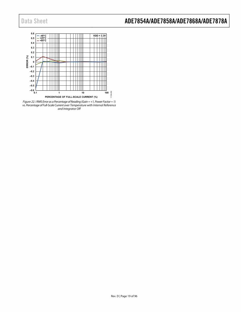
Figure 22 I RMS Error as a Percentage of Reading (Gain = +1 Power Factor = 1) vs Percentage of Full-Scale Current over Temperature with Internal Reference
and Integrator Off
ADE7854AADE7858AADE7868AADE7878A Data Sheet
Rev D | Page 20 of 96
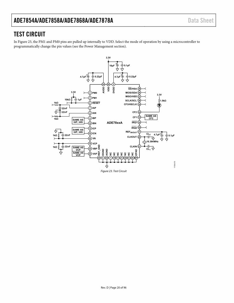
TEST CIRCUIT In Figure 23 the PM1 and PM0 pins are pulled up internally to VDD Select the mode of operation by using a microcontroller to programmatically change the pin values (see the Power Management section)
SAME ASCF2
PM0
022microF47microF
MOSISDA
MISOHSD
SCLKSCL
CF3HSCLK
CF2
CF1
REFINOUT
CLKOUT
CLKIN
PM1
RESET
IAP
IAN
IBP
IBN
ICP
ICN
VN
VCP
VBP
VAP
2
23
3
4
7
8
9
12
13
14
18
19
22
39
38
37
36
35
34
33
32
29
17
28
27
ADE78xxA
24 26 5
AV
DD
VD
D
DV
DD
6
DG
ND
25
AG
ND
1
NC
10
NC
11
NC
21
NC
30
NC
31
NC
40
NC
EP
EP
AD
20
RE
F_G
ND
022microF47microF
01microF47microF+
+ +
01microF10microF+
CL2
CL1
16384MHz
SAME ASVCP
SAME ASVCP
SAME ASIAP IAN
SAME ASIAP IAN
22nF1kΩ
1kΩ
1kΩ10kΩ 15kΩ
1kΩ 22nF
33V
33V
33V
1microF
22nF
22nF
SSHSA
IRQ1
IRQ0
1113
6-0
15
Figure 23 Test Circuit
Data Sheet ADE7854AADE7858AADE7868AADE7878A
Rev D | Page 21 of 96
TERMINOLOGY Measurement Error The error associated with the energy measurement made by the ADE7854AADE7858AADE7868AADE7878A is defined as follows
Measurement Error =
100
EnergyTrueEnergyTrue DevicebyRegisteredEnergy
(1)
where Device represents the ADE7854A ADE7858A ADE7868A or ADE7878A
Power Supply Rejection (PSR) PSR quantifies the ADE7854AADE7858AADE7868A ADE7878A measurement error as a percentage of reading when the power supplies are varied For the ac PSR measurement a reading at nominal supplies (33 V) is taken A second reading is obtained with the same input signal levels when an ac signal (120 mV rms at twice the fundamental frequency) is introduced onto the supplies Any error introduced by this ac signal is expressed as a percentage of reading
For the dc PSR measurement a reading at nominal supplies (33 V) is taken A second reading is obtained with the same input signal levels when the power supplies are varied by plusmn10 Any error introduced is expressed as a percentage of the reading
ADC Offset ADC offset refers to the dc offset associated with the analog inputs to the ADCs It means that with the analog inputs connected to AGND the ADCs still see a dc analog input signal The magnitude of the offset depends on the gain and input range selection The high-pass filter (HPF) removes the offset from the current and voltage channels therefore the power calculation remains unaffected by this offset
Gain Error The gain error in the ADCs of the ADE7854AADE7858A ADE7868AADE7878A is defined as the difference between the measured ADC output code (minus the offset) and the ideal output code (see the Current Channel ADC and Voltage Channel ADC sections) The difference is expressed as a percentage of the ideal code
CF Jitter The period of pulses at one of the CF1 CF2 or CF3HSCLK pins is continuously measured The maximum minimum and average values of four consecutive pulses are computed as follows
Maximum = max(Period0 Period1 Period2 Period3)
Minimum = min(Period0 Period1 Period2 Period3)
Average = 4
3210 PeriodPeriodPeriodPeriod
The CF jitter is then computed as follows
100
Average
MinimumMaximumCFJITTER (2)
Signal-to-Noise Ratio (SNR) SNR is the ratio of the rms value of the actual input signal to the rms sum of all other spectral components below 2 kHz excluding harmonics and dc The input signal contains only the fundamental component The spectral components are calculated over a 2 sec window The value for SNR is expressed in decibels
Signal-to-Noise-and-Distortion (SINAD) Ratio SINAD is the ratio of the rms value of the actual input signal to the rms sum of all other spectral components below 2 kHz including harmonics but excluding dc The input signal contains only the fundamental component The spectral components are calculated over a 2 sec window The value for SINAD is expressed in decibels
ADE7854AADE7858AADE7868AADE7878A Data Sheet
Rev D | Page 22 of 96
POWER MANAGEMENT The ADE7868AADE7878A have four modes of operation and the ADE7854AADE7858A have two modes of operation the modes of operation are determined by the state of the PM0 and PM1 pins (see Table 9)
Table 9 Power Supply Modes Power Supply Mode PM1 Pin PM0 Pin PSM0 Normal Power Mode 0 1 PSM1 Reduced Power Mode1 0 0 PSM2 Low Power Mode1 1 0 PSM3 Sleep Mode 1 1 1 Available in the ADE7868A and ADE7878A only
The PM1 and PM0 pins control the operation of the ADE7854A ADE7858AADE7868AADE7878A These pins are easily con-nected to an external microprocessor inputoutput The PM1 and PM0 pins include internal pull-up resistors therefore the ADE7854AADE7858AADE7868AADE7878A are in sleep mode by default For recommended actions to take before and after setting a new power mode see Table 11 and Table 12
PSM0 NORMAL POWER MODE (ALL DEVICES) In PSM0 normal power mode (PSM0 mode) the ADE7854A ADE7858AADE7868AADE7878A are fully functional To enter PSM0 mode the PM1 pin is set low and the PM0 pin is set high When a device is in PSM1 PSM2 or PSM3 mode and switches to PSM0 mode all control registers revert to their default values except for the threshold register LPOILVL (which is used in PSM2 mode) and the CONFIG2 register These registers maintain their programmed values
The ADE7854AADE7858AADE7868AADE7878A signal the completion of the power-up procedure by driving the IRQ1 interrupt pin low and setting Bit 15 (RSTDONE) in the STATUS1 register to 1 Bit 15 is cleared to 0 during the power-up sequence and is set to 1 when the chip enters PSM0 mode Writing to the STATUS1 register with the RSTDONE bit set to 1 clears the status bit and returns the IRQ1 pin high
The RSTDONE interrupt cannot be masked because Bit 15 (RSTDONE) in the interrupt mask register has no functionality
PSM1 REDUCED POWER MODE (ADE7868A AND ADE7878A ONLY) The PSM1 reduced power mode (PSM1 mode) is available on the ADE7868A and ADE7878A only In PSM1 mode the ADE7868AADE7878A measure the mean absolute values (MAV) of the 3-phase currents and store the results in the 20-bit AIMAV BIMAV and CIMAV registers PSM1 mode is useful in missing neutral cases where an external battery provides the voltage supply for the ADE7868A or ADE7878A
The I2C or SPI serial port is enabled in PSM1 mode and can be used to read the AIMAV BIMAV and CIMAV registers Do not read any other registers because their values are not guaranteed in PSM1 mode Similarly a write operation in PSM1 mode is ignored by the ADE7868AADE7878A In PSM1 mode do not access any registers other than AIMAV BIMAV and CIMAV For more information about the xIMAV registers see the Current Mean Absolute Value CalculationmdashADE7868A and ADE7878A Only section
The circuit that measures the estimates of rms values is also active during PSM0 mode therefore the calibration of this circuit can be done in either PSM0 mode or PSM1 mode Note that the ADE7868A and ADE7878A do not provide registers to store or process the corrections resulting from the calibration process The external microprocessor stores the gain values from these measurements and uses them during PSM1 mode
The 20-bit mean absolute value measurements that are completed in PSM1 mode are available in PSM0 mode However the MAV values are different from the rms measurements of phase currents and voltages that are executed only in PSM0 mode and stored in the xIRMS and xVRMS 24-bit registers For more information see the Current Mean Absolute Value CalculationmdashADE7868A and ADE7878A Only section
If the ADE7868AADE7878A are set to PSM1 mode while configured for PSM0 mode the devices immediately begin the mean absolute value calculations The xIMAV registers are accessible at any time however if the ADE7878A or ADE7868A is set to PSM1 mode while configured for PSM2 or PSM3 mode the ADE7868AADE7878A signal the start of the mean absolute value computations by driving the IRQ1 pin low The xIMAV registers can be accessed only after the IRQ1 pin is low
PSM2 LOW POWER MODE (ADE7868A AND ADE7878A ONLY) The PSM2 low power mode (PSM2 mode) is available on the ADE7868A and ADE7878A only PSM2 mode reduces the power consumption required to monitor the currents when there is no voltage input and an external battery provides the voltage supply for the ADE7868AADE7878A
PSM2 mode detects a missing neutral tamper condition by monitoring all phase currents and comparing them with a programmable threshold If any phase current rises above the programmable threshold for a programmable period the device assumes that a tamper attack has occurred If all currents remain below the programmable threshold no tamper attack has taken place instead a simple power outage has occurred
When a missing neutral tamper condition occurs the external microprocessor sets the ADE7868AADE7878A to PSM1 mode measures the mean absolute values of the phase currents and integrates the energy based on these values and the nominal voltage The I2C or SPI port is not functional during this mode
Data Sheet ADE7854AADE7858AADE7868AADE7878A
Rev D | Page 23 of 96
It is best practice to use the ADE7868AADE7878A in PSM2 mode when the PGA1 gain is 1 or 2 PGA1 represents the gain in the current channel datapath Do not use the ADE7868A or ADE7878A in PSM2 mode when the PGA1 gain is 4 8 or 16
Two PSM2 modes of operation are available PSM2 interrupt mode and PSM2 IRQ1 only mode The PSM2 interrupt mode is the default mode If the use of an external timer is possible use the PSM2 IRQ1 only mode
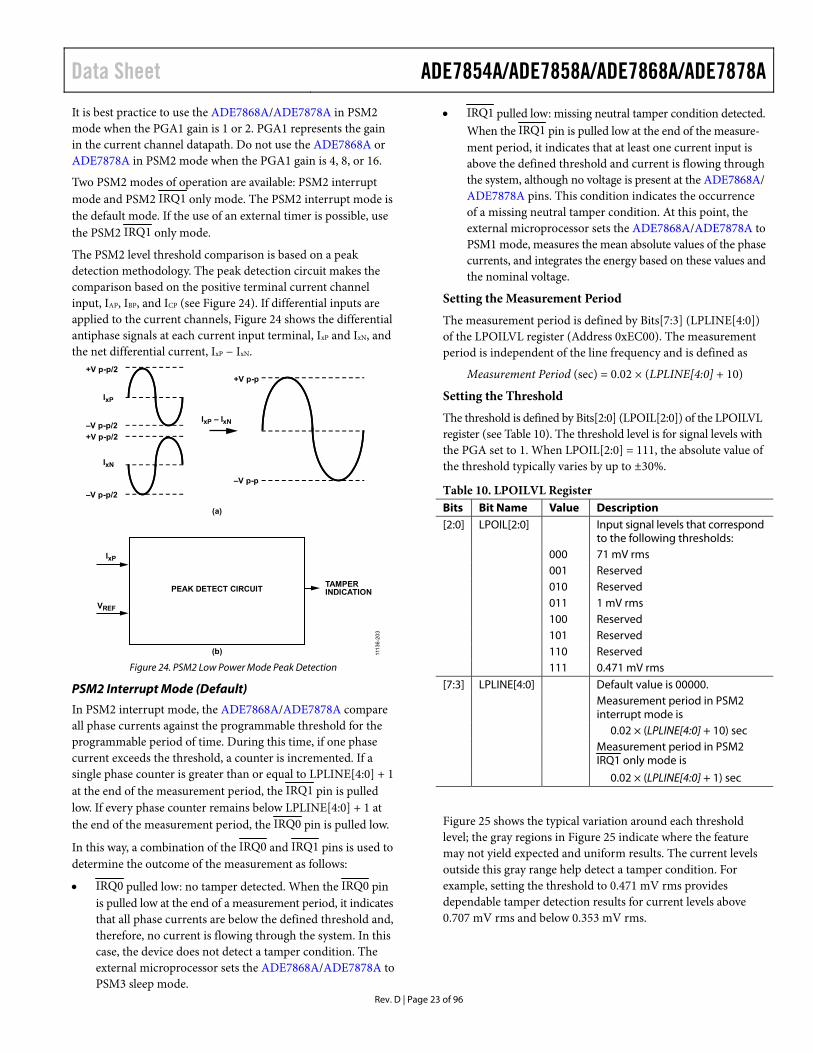
The PSM2 level threshold comparison is based on a peak detection methodology The peak detection circuit makes the comparison based on the positive terminal current channel input IAP IBP and ICP (see Figure 24) If differential inputs are applied to the current channels Figure 24 shows the differential antiphase signals at each current input terminal IxP and IxN and the net differential current IxP minus IxN
VREF
IxP
IxN
TAMPERINDICATION
+V p-p
ndashV p-p
ndashV p-p2
ndashV p-p2
+V p-p2
+V p-p2
PEAK DETECT CIRCUIT
IxP ndash IxN
IxP
(a)
(b) 111
36-2
03
Figure 24 PSM2 Low Power Mode Peak Detection
PSM2 Interrupt Mode (Default)
In PSM2 interrupt mode the ADE7868AADE7878A compare all phase currents against the programmable threshold for the programmable period of time During this time if one phase current exceeds the threshold a counter is incremented If a single phase counter is greater than or equal to LPLINE[40] + 1 at the end of the measurement period the IRQ1 pin is pulled low If every phase counter remains below LPLINE[40] + 1 at the end of the measurement period the IRQ0 pin is pulled low
In this way a combination of the IRQ0 and IRQ1 pins is used to determine the outcome of the measurement as follows
IRQ0 pulled low no tamper detected When the IRQ0 pin is pulled low at the end of a measurement period it indicates that all phase currents are below the defined threshold and therefore no current is flowing through the system In this case the device does not detect a tamper condition The external microprocessor sets the ADE7868AADE7878A to PSM3 sleep mode
IRQ1 pulled low missing neutral tamper condition detected When the IRQ1 pin is pulled low at the end of the measure-ment period it indicates that at least one current input is above the defined threshold and current is flowing through the system although no voltage is present at the ADE7868A ADE7878A pins This condition indicates the occurrence of a missing neutral tamper condition At this point the external microprocessor sets the ADE7868AADE7878A to PSM1 mode measures the mean absolute values of the phase currents and integrates the energy based on these values and the nominal voltage
Setting the Measurement Period
The measurement period is defined by Bits[73] (LPLINE[40]) of the LPOILVL register (Address 0xEC00) The measurement period is independent of the line frequency and is defined as
Measurement Period (sec) = 002 times (LPLINE[40] + 10)
Setting the Threshold
The threshold is defined by Bits[20] (LPOIL[20]) of the LPOILVL register (see Table 10) The threshold level is for signal levels with the PGA set to 1 When LPOIL[20] = 111 the absolute value of the threshold typically varies by up to plusmn30
Table 10 LPOILVL Register Bits Bit Name Value Description [20] LPOIL[20] Input signal levels that correspond
to the following thresholds 000 71 mV rms 001 Reserved 010 Reserved 011 1 mV rms 100 Reserved 101 Reserved 110 Reserved 111 0471 mV rms
[73] LPLINE[40] Default value is 00000 Measurement period in PSM2 interrupt mode is
002 times (LPLINE[40] + 10) sec Measurement period in PSM2 IRQ1 only mode is
002 times (LPLINE[40] + 1) sec
Figure 25 shows the typical variation around each threshold level the gray regions in Figure 25 indicate where the feature may not yield expected and uniform results The current levels outside this gray range help detect a tamper condition For example setting the threshold to 0471 mV rms provides dependable tamper detection results for current levels above 0707 mV rms and below 0353 mV rms
ADE7854AADE7858AADE7868AADE7878A Data Sheet
Rev D | Page 24 of 96
71mV rms79mV rms
RATIO TOFULL SCALE
64mV rms
1mV rms LPOIL[20] = 011
LPOIL[20] = 000
LPOIL[20] = 111
118mV rms
088mV rms
0471mV rms
0707mV rms
0353mV rms
111
36
-12
4
DETECTSTAMPERCONDITIONSABOVETHIS LEVEL
DETECTS NONTAMPERCONDITIONS
BELOWTHIS LEVEL
Figure 25 Variation Around Each Threshold Setting
Figure 26 shows the behavior of the ADE7868AADE7878A PSM2 mode when LPLINE[40] = 2 The test period is 12 cycles at 50 Hz (240 ms) the Phase A current rises above the LPOIL[20] threshold five times Because the counter value is above the internal counter requirement of LPLINE[40] + 1 the IRQ1 pin is pulled low at the end of the test period This result suggests that a missing neutral tamper condition has occurred
PSM2 IRQ1 Only Mode
The PSM2 IRQ1 only mode uses only the IRQ1 pin to indicate a tamper event If no tamper event has occurred no signal is provided by the ADE7868A or ADE7878A
To disable the IRQ0 pin and thus enable the PSM2 IRQ1 only mode set Bit 2 (IRQ0_DIS) in the CONFIG2 register (Address 0xEC01) to 1 Selecting this mode defines the recommended measurement period using the following formula
Recommended Measurement Period (sec) = 002 times (LPLINE[40] + 1)
Because a wait is required during this measurement period use an external timer before checking the status of the IRQ1 interrupt The measurement period can be longer than the recommended period because the internal phase counter continues to increment for the entire time that the device is in PSM2 mode Switching to PSM3 mode and then back to PSM2 mode causes the device to enter the PSM2 interrupt mode (the default PSM2 mode)
PSM3 SLEEP MODE (ALL DEVICES) PSM3 sleep mode is available on all devices ADE7854A ADE7858A ADE7868A and ADE7878A In sleep mode most of the internal circuits in the devices are turned off and the current consumption is at its lowest level When configuring the device for sleep mode set the RESET SCLKSCL MOSISDA and SSHSA pins high
In PSM3 sleep mode the I2C HSDC and SPI ports are not functional
LPLINE[40] = 2
MEASUREMENT PERIOD = 12 CYCLES (50Hz)
LPOIL[20]THRESHOLD
IA CURRENT
PH
AS
EC
OU
NT
ER
= 1
PH
AS
EC
OU
NT
ER
= 2
PH
AS
EC
OU
NT
ER
= 3
PH
AS
EC
OU
NT
ER
= 4
PH
AS
EC
OU
NT
ER
= 5
IRQ1
AS PHASE COUNTER gt LPLINE[40] +1 IRQ1 IS TRIGGERED
111
36-
016
Figure 26 PSM2 Interrupt Mode Triggering IRQ1 Pin for LPLINE[40] = 2 (50 Hz Systems)
Data Sheet ADE7854AADE7858AADE7868AADE7878A
Rev D | Page 25 of 96
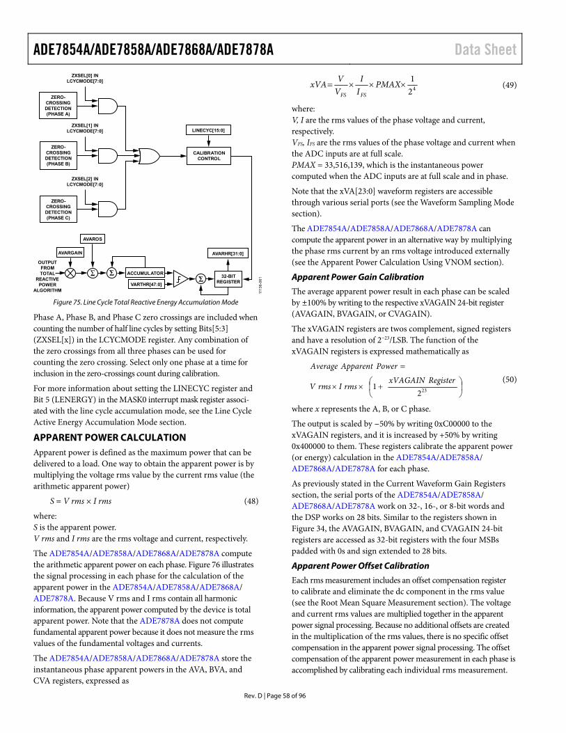
Table 11 Power Modes and Related Characteristics
Power Mode LPOILVL and CONFIG2 Registers All Other Registers1 I2CSPI Port Functionality
PSM0 After Hardware Reset Set to default values Set to default values I2C port enabled All circuits are active and DSP is in
idle mode After Software Reset Unchanged Set to default values If the lock-in procedure was
previously executed the active serial port is unchanged
All circuits are active and DSP is in idle mode
PSM1 (ADE7868A and ADE7878A Only)
Values set during PSM0 mode are unchanged
Not available I2C or SPI port enabled but with limited functionality
Current mean absolute values are computed and the results are stored in the AIMAV BIMAV and CIMAV registers
PSM2 (ADE7868A and ADE7878A Only)
Values set during PSM0 mode are unchanged
Not available Serial port disabled Compares phase currents against the threshold set in the LPOILVL register and triggers the IRQ0 or IRQ1 pin accordingly
PSM3 Values set during PSM0 mode are unchanged
Not available Serial port disabled Internal circuits are shut down
1 Setting for all registers except the LPOILVL and CONFIG2 registers
Table 12 Recommended Actions When Changing Power Modes
Initial Power Mode
Recommended Actions Before Setting Next Power Mode
Next Power Mode
PSM0 PSM1 PSM2 PSM3 PSM0 Stop the DSP by setting
the run register to 0x0000
Current mean absolute values (MAV) computed immediately
Wait until the IRQ0 or IRQ1 pin is pulled low
No action necessary
Disable HSDC by clearing Bit 6 (HSDCEN) to 0 in the CONFIG register
xIMAV registers immediately accessible
Mask interrupts by setting MASK0 and MASK1 registers to 0x0
Erase interrupt status flags in the STATUS0 and STATUS1 registers
PSM1 (ADE7868A and ADE7878A Only)
No action necessary Wait until the IRQ1 pin is pulled low
Wait until the IRQ0 or IRQ1 pin is pulled low
No action necessary
Poll the STATUS1 register until Bit 15 (RSTDONE) is set to 1
PSM2 (ADE7868A and ADE7878A Only)
No action necessary Wait until the IRQ1 pin is pulled low
Wait until the IRQ1 pin is pulled low
No action necessary
Poll the STATUS1 register until Bit 15 (RSTDONE) is set to 1
Current mean absolute values computed after IRQ1 pin is pulled low
xIMAV registers accessible after IRQ1 pin is pulled low
PSM3 No action necessary Wait until the IRQ1 pin is pulled low
Wait until the IRQ1 pin is pulled low
Wait until the IRQ0 or IRQ1 pin is pulled low
Poll the STATUS1 register until Bit 15 (RSTDONE) is set to 1
Current mean absolute values computed after IRQ1 pin is pulled low
xIMAV registers accessible after IRQ1 pin is pulled low
ADE7854AADE7858AADE7868AADE7878A Data Sheet
Rev D | Page 26 of 96
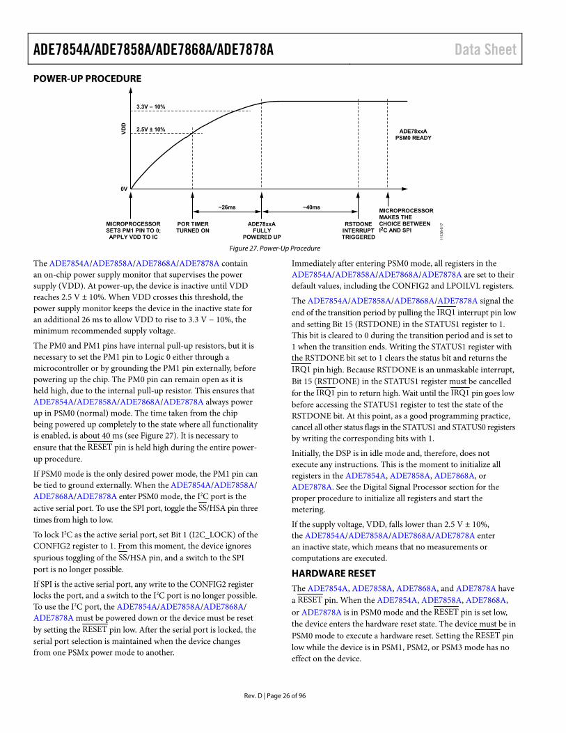
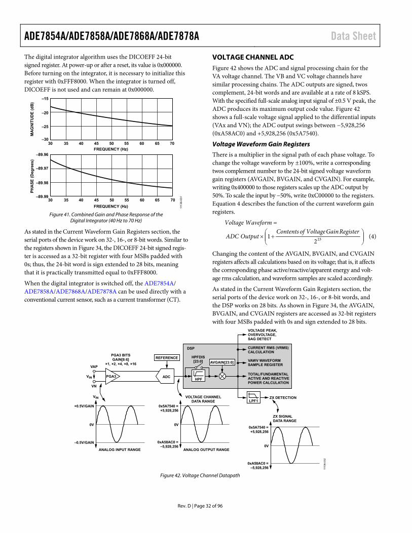
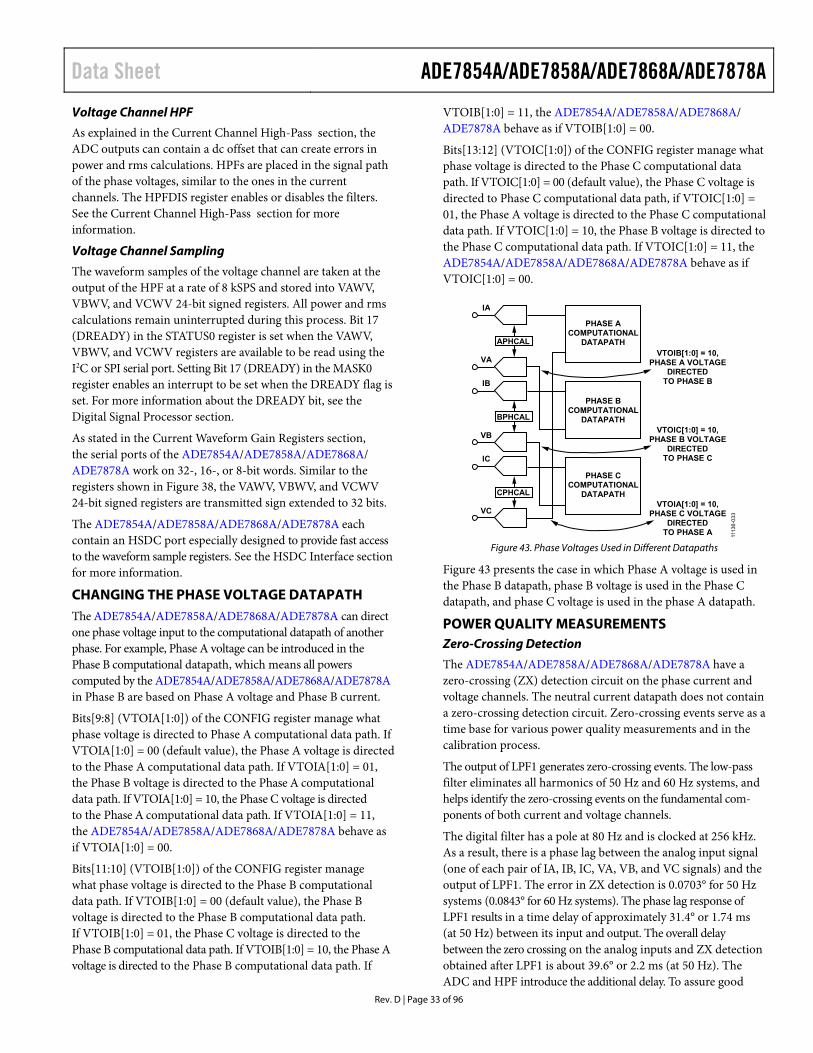
POWER-UP PROCEDURE
POR TIMERTURNED ON
ADE78xxAFULLY
POWERED UP
MICROPROCESSORMAKES THECHOICE BETWEENI2C AND SPI
MICROPROCESSORSETS PM1 PIN TO 0APPLY VDD TO IC
RSTDONEINTERRUPTTRIGGERED
~40ms~26ms
0V
VD
D
33V ndash 10
25V plusmn 10 ADE78xxAPSM0 READY
111
36-
01
7
Figure 27 Power-Up Procedure
The ADE7854AADE7858AADE7868AADE7878A contain an on-chip power supply monitor that supervises the power supply (VDD) At power-up the device is inactive until VDD reaches 25 V plusmn 10 When VDD crosses this threshold the power supply monitor keeps the device in the inactive state for an additional 26 ms to allow VDD to rise to 33 V minus 10 the minimum recommended supply voltage
The PM0 and PM1 pins have internal pull-up resistors but it is necessary to set the PM1 pin to Logic 0 either through a microcontroller or by grounding the PM1 pin externally before powering up the chip The PM0 pin can remain open as it is held high due to the internal pull-up resistor This ensures that ADE7854AADE7858AADE7868AADE7878A always power up in PSM0 (normal) mode The time taken from the chip being powered up completely to the state where all functionality is enabled is about 40 ms (see Figure 27) It is necessary to ensure that the RESET pin is held high during the entire power-up procedure
If PSM0 mode is the only desired power mode the PM1 pin can be tied to ground externally When the ADE7854AADE7858A ADE7868AADE7878A enter PSM0 mode the I2C port is the active serial port To use the SPI port toggle the SSHSA pin three times from high to low
To lock I2C as the active serial port set Bit 1 (I2C_LOCK) of the CONFIG2 register to 1 From this moment the device ignores spurious toggling of the SSHSA pin and a switch to the SPI port is no longer possible
If SPI is the active serial port any write to the CONFIG2 register locks the port and a switch to the I2C port is no longer possible To use the I2C port the ADE7854AADE7858AADE7868A ADE7878A must be powered down or the device must be reset by setting the RESET pin low After the serial port is locked the serial port selection is maintained when the device changes from one PSMx power mode to another
Immediately after entering PSM0 mode all registers in the ADE7854AADE7858AADE7868AADE7878A are set to their default values including the CONFIG2 and LPOILVL registers
The ADE7854AADE7858AADE7868AADE7878A signal the end of the transition period by pulling the IRQ1 interrupt pin low and setting Bit 15 (RSTDONE) in the STATUS1 register to 1 This bit is cleared to 0 during the transition period and is set to 1 when the transition ends Writing the STATUS1 register with the RSTDONE bit set to 1 clears the status bit and returns the IRQ1 pin high Because RSTDONE is an unmaskable interrupt Bit 15 (RSTDONE) in the STATUS1 register must be cancelled for the IRQ1 pin to return high Wait until the IRQ1 pin goes low before accessing the STATUS1 register to test the state of the RSTDONE bit At this point as a good programming practice cancel all other status flags in the STATUS1 and STATUS0 registers by writing the corresponding bits with 1
Initially the DSP is in idle mode and therefore does not execute any instructions This is the moment to initialize all registers in the ADE7854A ADE7858A ADE7868A or ADE7878A See the Digital Signal Processor section for the proper procedure to initialize all registers and start the metering
If the supply voltage VDD falls lower than 25 V plusmn 10 the ADE7854AADE7858AADE7868AADE7878A enter an inactive state which means that no measurements or computations are executed
HARDWARE RESET The ADE7854A ADE7858A ADE7868A and ADE7878A have a RESET pin When the ADE7854A ADE7858A ADE7868A or ADE7878A is in PSM0 mode and the RESET pin is set low the device enters the hardware reset state The device must be in PSM0 mode to execute a hardware reset Setting the RESET pin low while the device is in PSM1 PSM2 or PSM3 mode has no effect on the device
Data Sheet ADE7854AADE7858AADE7868AADE7878A
Rev D | Page 27 of 96
When the ADE7854A ADE7858A ADE7868A or ADE7878A is in PSM0 mode and the RESET pin is toggled from high to low and then back to high after at least 10 μs all registers are reset to their default values including the CONFIG2 and LPOILVL registers
The device signals the end of the transition period by pulling the IRQ1 interrupt pin low and setting Bit 15 (RSTDONE) in the STATUS1 register to 1 This bit is cleared to 0 during the transition period and is reset to 1 when the transition ends Writing to the STATUS1 register with the RSTDONE bit set to 1 clears the status bit and returns the IRQ1 pin high
After a hardware reset the DSP is in idle mode and therefore does not execute any instructions
Because the I2C port is the default serial port of the ADE7854A ADE7858AADE7868AADE7878A it becomes active after a reset If the SPI is the port used by the external microprocessor the procedure to enable it must be repeated immediately after the RESET pin is toggled back to high (for more information see the Serial Interface Selection section)
After a hardware reset initialize all registers of the ADE7854A ADE7858AADE7868AADE7878A registers enable data memory RAM protection and then write 0x0001 to the run register to start the DSP For more information about data memory RAM protection and the run register see the Digital Signal Processor section
SOFTWARE RESET Bit 7 (SWRST) in the CONFIG register manages the software reset functionality in PSM0 mode The default value of this bit is 0 Setting Bit 7 to 1 causes the ADE7854AADE7858A ADE7868AADE7878A to enter the software reset state In this state all internal registers except for CONFIG2 and LPOILVL are reset to their default values The selected serial port I2C or SPI remains unchanged if the lock-in procedure was executed (see the Serial Interface Selection section)
When the software reset ends Bit 7 (SWRST) in the CONFIG register is cleared to 0 the IRQ1 interrupt pin is set low and Bit 15 (RSTDONE) in the STATUS1 register is set to 1 The RSTDONE bit is cleared to 0 during the transition period and is reset to 1 when the transition ends Writing to the STATUS1 register with the RSTDONE bit set to 1 clears the status bit and resets the IRQ1 pin high
After software reset the DSP is in idle mode and therefore does not execute any instructions Take the following steps to restart the DSP
1 Initialize all ADE7854AADE7858AADE7868A ADE7878A registers
2 Enable the data memory RAM protection 3 Write 0x0001 to the run register to start the DSP For more
information about data memory RAM protection and the run register see the Digital Signal Processor section
The software reset functionality is not available in PSM1 PSM2 or PSM3 mode
ADE7854AADE7858AADE7868AADE7878A Data Sheet
Rev D | Page 28 of 96
THEORY OF OPERATION ANALOG INPUTS The ADE7868AADE7878A have seven analog inputs forming current and voltage channels The ADE7854AADE7858A have six analog inputs but the neutral current is removed from these devices
The current channels consist of four pairs of fully differential voltage inputs IAP and IAN IBP and IBN ICP and ICN and INP and INN These voltage input pairs have a maximum differential signal of plusmn05 V peak In addition the maximum signal level on analog inputs for each IxPIxN pair is plusmn05 V peak with respect to AGND The maximum common-mode signal allowed on the inputs is plusmn25 mV Figure 28 shows a schematic of the input for the current channels and their relationship to the maximum common-mode voltage
IAP IBPICP OR INP
IAN IBNICN OR INN
V1
V2
+500mV
VCM
V1 + V2
DIFFERENTIAL INPUTV1 + V2 = 500mV MAX PEAK
COMMON MODEVCM = plusmn25mV MAX
ndash500mV VCM
111
36-
02
1
Figure 28 Maximum Input Level Current Channels Gain = +1
All inputs have a programmable gain amplifier (PGA) with a possible gain selection of 1 2 4 8 or 16 The gain of the IAx IBx and ICx inputs is set in Bits[20] (PGA1[20]) of the gain register For the ADE7868A and ADE7878A only the gain of the INx channel input is set in Bits[53] (PGA2[20]) of the gain register thus a different gain from the IAx IBx or ICx inputs is possible See Table 42 for information about the gain register The voltage channel has three single-ended voltage inputs VAP VBP and VCP These single-ended voltage inputs have a maximum input voltage of plusmn05 V with respect to VN In addition the maximum signal level on analog inputs for VxP and VN is plusmn05 V with respect to AGND The maximum common-mode signal allowed on the inputs is plusmn25 mV See Figure 29 for a schematic of the voltage channel inputs and their relationship to the maximum common-mode voltage
VAP VBPOR VCP
VNVCM
V1
+500mV
VCM
V1
SINGLE-ENDED INPUTV1 = 500mV MAX PEAK
COMMON MODEVCM = plusmn25mV MAX
ndash500mV
111
36
-01
8
Figure 29 Maximum Input Level Voltage Channels Gain = +1
All inputs have a programmable gain with a possible gain selection of 1 2 4 8 or 16 To set the gain use Bits[86] (PGA3[20]) in the gain register (see Table 42)
Figure 30 shows how the gain selection from the gain register works in both the current and voltage channels
K times VIN
GAINSELECTION
IxN VN
IxP VyP
VIN
NOTES1 x = A B C N y = A B C 11
136
-02
0
Figure 30 PGA in Current and Voltage Channels
ANALOG-TO-DIGITAL CONVERSION The ADE7868AADE7878A have seven Σ-Δ analog-to-digital converters (ADCs) and the ADE7854A ADE7858A have six Σ-Δ ADCs
In PSM0 mode all ADCs are active In PSM1 mode only the ADCs that measure the Phase A
Phase B and Phase C currents are active The ADCs that measure the neutral current and the A B and C phase voltages are turned off
In PSM2 and PSM3 modes the ADCs are powered down to minimize power consumption
For simplicity the block diagram in Figure 31 shows a first-order Σ-Δ ADC The converter is composed of the Σ-Δ modulator and the digital low-pass filter
24
DIGITALLOW-PASS
FILTERR
C
+
ndash
CLKIN16
INTEGRATOR
VREF
1-BIT DAC
LATCHEDCOMPARATOR
ANALOGLOW-PASS FILTER
10100101
+ndash
111
36
-01
9
Figure 31 First-Order -∆ ADC
The Σ-Δ modulator converts the input signal into a continuous serial stream of 1s and 0s at a rate determined by the sampling clock In the ADE7854AADE7858AADE7868AADE7878A the sampling clock is equal to 1024 MHz (CLKIN16)
The 1-bit DAC in the feedback loop is driven by the serial data stream The DAC output is subtracted from the input signal When the loop gain is high enough the average value of the DAC output (and therefore the bit stream) can approach that of the input signal level For any given input value in a single sampling interval the data from the 1-bit ADC is virtually meaningless Only when a large number of samples are averaged is a meaningful result obtained This averaging occurs in the second part of the ADC (the digital low-pass filter) By averaging a large number of bits from the modulator the low-pass filter can produce 24-bit data-words that are proportional to the input signal level
Data Sheet ADE7854AADE7858AADE7868AADE7878A
Rev D | Page 29 of 96
The Σ-Δ ADC uses two techniques to achieve high resolution from what is essentially a 1-bit conversion technique The first technique is oversampling Oversampling means that the signal is sampled at a rate (frequency) that is many times higher than the bandwidth of interest For example the sampling rate in the ADE7854AADE7858AADE7868AADE7878A is 1024 MHz and the bandwidth of interest is 40 Hz to 2 kHz
Oversampling has the effect of spreading the quantization noise (noise due to sampling) over a wider bandwidth With the noise spread more thinly over a wider bandwidth the quantization noise in the band of interest lowers as shown in Figure 32 However oversampling alone is not efficient enough to improve the signal-to-noise ratio (SNR) in the band of interest For example an oversampling factor of 4 is required just to increase the SNR by a mere 6 dB (one bit) To keep the oversampling ratio at a reasonable level it is possible to shape the quantization noise so that the majority of the noise lies at the higher frequencies
In the Σ-Δ modulator the noise is shaped by the integrator which has a high-pass-type response for the quantization noise This is the second technique used to achieve high resolution The result is that most of the noise is at the higher frequencies where the digital low-pass filter removes it This noise shaping is shown in Figure 32
NOISE
SIGNAL
NOISE
SIGNAL
0 2 4 512FREQUENCY (kHz)
HIGH RESOLUTIONOUTPUT FROMDIGITAL LPF
1024
0 2 4 512FREQUENCY (kHz)
1024
DIGITAL FILTERSHAPED NOISE
ANTIALIAS FILTER(RC)
SAMPLINGFREQUENCY
1113
6-0
22
Figure 32 Noise Reduction Due to Oversampling and
Noise Shaping in the Analog Modulator
Antialiasing Filter
Figure 31 shows an analog low-pass filter (RC) on the input to the ADC This filter is placed outside the ADE7854AADE7858A ADE7868AADE7878A its role is to prevent aliasing Aliasing is an artifact of all sampled systems as shown in Figure 33 Aliasing means that frequency components in the input signal to the ADC which are higher than half the sampling rate of the ADC appear in the sampled signal at a frequency below half the sampling rate Frequency components above half the sampling frequency (also known as the Nyquist frequency that is 512 kHz) are imaged or folded back down below 512 kHz This happens with all ADCs regardless of the architecture In the example shown only frequen-cies near the sampling frequency that is 1024 MHz move into
the band of interest for metering that is 40 Hz to 2 kHz To attenuate the high frequency noise (near 1024 MHz) and prevent the distortion of the band of interest a low-pass filter (LPF) must be introduced
For conventional current sensors use one RC filter with a corner frequency of 5 kHz to achieve sufficiently high attenuation at the sampling frequency of 1024 MHz The 20 dB per decade attenuation of this filter is usually sufficient to eliminate the effects of aliasing for conventional current sensors However for a didt sensor such as a Rogowski coil the sensor has a 20 dB per decade gain This neutralizes the 20 dB per decade attenuation produced by the LPF Therefore when using a didt sensor take care to offset the 20 dB per decade gain One simple approach is to cascade one additional RC filter thereby producing a minus40 dB per decade attenuation
ALIASING EFFECTSSAMPLING
FREQUENCY
IMAGEFREQUENCIES
0 2 4 512
FREQUENCY (kHz)
1024
111
36
-02
3
Figure 33 Aliasing Effects
ADC Transfer Function
All ADCs in the ADE7854AADE7858AADE7868A ADE7878A are designed to produce the same 24-bit signed output code for the same input signal level With a full-scale input signal of 05 V and an internal reference of 12 V the ADC output code is nominally 5928256 (0x5A7540) The code from the ADC can vary between 0x800000 (minus8388608) and 0x7FFFFF (+8388607) this is equivalent to an input signal level of plusmn0707 V However for specified performance do not exceed the nominal range of plusmn05 V peak ADC performance is guaranteed only for input signals lower than plusmn05 V peak
CURRENT CHANNEL ADC Figure 35 shows the ADC and signal processing path for the IA current channel It is the same for the IB and IC current channels The ADC outputs are signed twos complement 24-bit data-words and are available at a rate of 8 kSPS (thousand samples per second) With the specified full-scale analog input signal of plusmn05 V peak the ADC produces its maximum output code value the ADC output swings between minus5928256 (0xA58AC0) and +5928256 (0x5A7540) Figure 35 shows a full-scale voltage signal applied to the differential inputs (IAP and IAN) The IN current channel corresponds to the neutral current of a 3-phase system (available in the ADE7868A and ADE7878A only) If no neutral line is present connect this input to AGND The datapath of the neutral current is similar to the path of the phase currents (see Figure 36)
ADE7854AADE7858AADE7868AADE7878A Data Sheet
Rev D | Page 30 of 96
Current Waveform Gain Registers
There is a multiplier in the signal path of each phase and neutral current The current waveform can be changed by plusmn100 by writing a corresponding twos complement number to the 24-bit signed current waveform gain registers (AIGAIN BIGAIN CIGAIN and NIGAIN) For example writing 0x400000 to the xIGAIN registers scales up the ADC output by 50 To scale the input by minus50 write 0xC00000 to these registers Equation 3 describes mathematically the function of the current waveform gain registers
Current Waveform =
232
1RegisterGainCurrentofContents
OutputADC (3)
Changing the content of the AIGAIN BIGAIN CIGAIN or NIGAIN register affects all calculations based on the current of
each of these registers that is it affects the corresponding phase activereactiveapparent energy and current rms calculation In addition waveform samples scale accordingly
Note that the serial ports of the ADE7854A ADE7858A ADE7868A and ADE7878A work on 32- 16- or 8-bit words and the DSP works on 28 bits The 24-bit AIGAIN BIGAIN CIGAIN and NIGAIN registers are accessed as 32-bit registers with the four most significant bits (MSBs) padded with 0s and sign extended to 28 bits (see Figure 34)
31 28 27 24 23 0
24-BIT NUMBER0000
BITS[2724] AREEQUAL TO BIT 23
BIT 23 IS A SIGN BIT
111
36
-02
6
Figure 34 24-Bit xIGAIN Registers Transmitted as 32-Bit Words
AIGAIN[230]
DSP
REFERENCE HPFDIS[230] DIGITAL
INTEGRATOR
INTEN BITCONFIG[0]
TOTALFUNDAMENTALACTIVE AND REACTIVEPOWER CALCULATION
CURRENT PEAKOVERCURRENTDETECT
IAWV WAVEFORMSAMPLE REGISTER
CURRENT RMS (IRMS)CALCULATION
HPFADCPGA1
IAP
ZX DETECTION
PGA1 BITSGAIN[20]
times1 times2 times4 times8 times16
VIN
VIN
IAN
ANALOG INPUT RANGE ADC OUTPUT RANGE
0x5A7540 =+5928256
ZX SIGNALDATA RANGE
0V
0xA58AC0 =ndash5928256
0x5A7540 =+5928256
CURRENT CHANNELDATA RANGE AFTER
INTEGRATION
0V
0xA58AC0 =ndash5928256
0x5A7540 =+5928256
CURRENT CHANNELDATA RANGE
0V
0xA58AC0 =ndash5928256
+05VGAIN
ndash05VGAIN
0V
LPF1
111
36-
02
4
Figure 35 Phase Current Signal Path
NIGAIN[230]
DSP
REFERENCE
DIGITALINTEGRATOR
INTEN BITCONFIG[0]
INWV WAVEFORMSAMPLE REGISTER
CURRENT RMS (IRMS)CALCULATION
HPFADCPGA2
INP
PGA2 BITSGAIN[53]
times1 times2 times4 times8 times16
VIN
INN
HPFDIS[230]
1113
6-0
25
Figure 36 Neutral Current Signal Path (ADE7868A and ADE7878A Only)
Data Sheet ADE7854AADE7858AADE7868AADE7878A
Rev D | Page 31 of 96
Current Channel High-Pass Filter
The ADC outputs can contain a dc offset This offset may create errors in power and rms calculations High-pass filters (HPFs) are placed in the signal path of the phase and neutral currents and of the phase voltages When enabled the HPF eliminates any dc offset on the current channel All filters are implemented in the DSP and by default they are all enabled the 24-bit HPFDIS register is cleared to 0x000000 Disable all filters by setting HPFDIS to any nonzero value
As stated in the Current Waveform Gain Registers section the serial ports of the ADE7854A ADE7858A ADE7868A and ADE7878A work on 32- 16- or 8-bit words The HPFDIS register is accessed as a 32-bit register with eight MSBs padded with 0s (see Figure 37)
31 24 23 0
24-BIT NUMBER0000 000011
13
6-0
27
Figure 37 24-Bit HPFDIS Register Transmitted as a 32-Bit Word
Current Channel Sampling
The waveform samples of the current channel are taken at the output of the HPF at a rate of 8 kSPS and stored in the 24-bit signed registers IAWV IBWV ICWV and INWV (ADE7868A and ADE7878A only) All power and rms calculations remain uninterrupted during this process Bit 17 (DREADY) in the STATUS0 register is set when the IAWV IBWV ICWV and INWV registers are available to be read using the I2C or SPI serial port Setting Bit 17 (DREADY) in the MASK0 register enables an interrupt to be set when the DREADY flag is set See the Digital Signal Processor section for more information about the DREADY bit
As stated in the Current Waveform Gain Registers section the serial ports of the ADE7854AADE7858AADE7868A ADE7878A work on 32- 16- or 8-bit words When the IAWV IBWV ICWV and INWV 24-bit signed registers are read from the device (INWV is available on ADE7868AADE7878A only) they are transmitted sign extended to 32 bits (see Figure 38)
31 24 23 22 0
24-BIT SIGNED NUMBER
BITS[3124] AREEQUAL TO BIT 23
BIT 23 IS A SIGN BIT
111
36
-02
8
Figure 38 24-Bit IxWV Registers Transmitted as 32-Bit Signed Words
The ADE7854AADE7858AADE7868AADE7878A contain a high speed data capture (HSDC) port that is specially designed to provide fast access to the waveform sample registers For more information see the HSDC Interface section
didt CURRENT SENSOR AND DIGITAL INTEGRATOR The didt sensor detects changes in the magnetic field caused by the ac current Figure 39 shows the principle of a didt current sensor
MAGNETIC FIELD CREATED BY CURRENT(DIRECTLY PROPORTIONAL TO CURRENT)
+ EMF (ELECTROMOTIVE FORCE)
ndash INDUCED BY CHANGES INMAGNETIC FLUX DENSITY (didt)
111
36
-02
9
Figure 39 Principle of a didt Current Sensor
The flux density of a magnetic field induced by a current is directly proportional to the magnitude of the current The changes in the magnetic flux density passing through a conductor loop generate an electromotive force (EMF) between the two ends of the loop The EMF is a voltage signal that is propor-tional to the didt of the current The mutual inductance between the current carrying conductor and the didt sensor determine the voltage output from the didt current sensor
The didt sensor requires filtering of the current signal before using it for power measurement On each phase and neutral current datapath there is a built-in digital integrator to recover the current signal from the didt sensor The digital integrator is disabled by default when the ADE7854AADE7858A ADE7868AADE7878A are powered up and after a reset Setting Bit 0 (INTEN) of the CONFIG register turns on the integrator Figure 40 and Figure 41 show the magnitude and phase response of the digital integrator
Note that the integrator has a minus20 dBdec attenuation and an approximately minus90deg phase shift When combined with a didt sensor the resulting magnitude and phase response should be a flat gain over the frequency band of interest However the didt sensor has a 20 dBdec gain associated with it and it generates significant high frequency noise An antialiasing filter of at least the second order is required to avoid noise aliasing back in the band of interest when the ADC is sampling (see the Antialiasing Filter section)
50
0
ndash50
ndash100
ndash50
0
MA
GN
ITU
DE
(d
B)
PH
AS
E (
Deg
rees
)
0 500 1000 1500 2000 2500 3000 3500 4000FREQUENCY (Hz)
001 01 1 10 100 1000FREQUENCY (Hz)
111
36
-03
0
Figure 40 Combined Gain and Phase Response of the Digital Integrator
ADE7854AADE7858AADE7868AADE7878A Data Sheet
Rev D | Page 32 of 96
The digital integrator algorithm uses the DICOEFF 24-bit signed register At power-up or after a reset its value is 0x000000 Before turning on the integrator it is necessary to initialize this register with 0xFFF8000 When the integrator is turned off DICOEFF is not used and can remain at 0x000000
ndash30
ndash15
ndash20
ndash25
ndash8996
ndash8997
ndash8998
ndash8999
MA
GN
ITU
DE
(d
B)
PH
AS
E (
Deg
rees
)
30 35 40 45 50 55 60 65 70
FREQUENCY (Hz)
30 35 40 45 50 55 60 65 70
FREQUENCY (Hz)
1113
6-0
31
Figure 41 Combined Gain and Phase Response of the
Digital Integrator (40 Hz to 70 Hz)
As stated in the Current Waveform Gain Registers section the serial ports of the device work on 32- 16- or 8-bit words Similar to the registers shown in Figure 34 the DICOEFF 24-bit signed regis-ter is accessed as a 32-bit register with four MSBs padded with 0s thus the 24-bit word is sign extended to 28 bits meaning that it is practically transmitted equal to 0xFFF8000
When the digital integrator is switched off the ADE7854A ADE7858AADE7868AADE7878A can be used directly with a conventional current sensor such as a current transformer (CT)
VOLTAGE CHANNEL ADC Figure 42 shows the ADC and signal processing chain for the VA voltage channel The VB and VC voltage channels have similar processing chains The ADC outputs are signed twos complement 24-bit words and are available at a rate of 8 kSPS With the specified full-scale analog input signal of plusmn05 V peak the ADC produces its maximum output code value Figure 42 shows a full-scale voltage signal applied to the differential inputs (VAx and VN) the ADC output swings between minus5928256 (0xA58AC0) and +5928256 (0x5A7540)
Voltage Waveform Gain Registers
There is a multiplier in the signal path of each phase voltage To change the voltage waveform by plusmn100 write a corresponding twos complement number to the 24-bit signed voltage waveform gain registers (AVGAIN BVGAIN and CVGAIN) For example writing 0x400000 to those registers scales up the ADC output by 50 To scale the input by minus50 write 0xC00000 to the registers Equation 4 describes the function of the current waveform gain registers
Voltage Waveform =
232
1RegisterGainVoltageofContents
OutputADC (4)
Changing the content of the AVGAIN BVGAIN and CVGAIN registers affects all calculations based on its voltage that is it affects the corresponding phase activereactiveapparent energy and volt-age rms calculation and waveform samples are scaled accordingly
As stated in the Current Waveform Gain Registers section the serial ports of the device work on 32- 16- or 8-bit words and the DSP works on 28 bits As shown in Figure 34 the AVGAIN BVGAIN and CVGAIN registers are accessed as 32-bit registers with four MSBs padded with 0s and sign extended to 28 bits
AVGAIN[230]REFERENCE HPFDIS
[230]
DSP
TOTALFUNDAMENTALACTIVE AND REACTIVEPOWER CALCULATION
VOLTAGE PEAKOVERVOLTAGESAG DETECT
VAWV WAVEFORMSAMPLE REGISTER
CURRENT RMS (VRMS)CALCULATION
HPFADCPGA3
VAP
ZX DETECTION
PGA3 BITSGAIN[86]
times1 times2 times4 times8 times16
VIN
VIN
VN
ANALOG INPUT RANGE ANALOG OUTPUT RANGE
0x5A7540 =+5928256
ZX SIGNALDATA RANGE
0V
0xA58AC0 =ndash5928256
0x5A7540 =+5928256
VOLTAGE CHANNELDATA RANGE
0V
0xA58AC0 =ndash5928256
+05VGAIN
ndash05VGAIN
0V
LPF1
111
36-0
32
Figure 42 Voltage Channel Datapath
Data Sheet ADE7854AADE7858AADE7868AADE7878A
Rev D | Page 33 of 96
Voltage Channel HPF
As explained in the Current Channel High-Pass section the ADC outputs can contain a dc offset that can create errors in power and rms calculations HPFs are placed in the signal path of the phase voltages similar to the ones in the current channels The HPFDIS register enables or disables the filters See the Current Channel High-Pass section for more information
Voltage Channel Sampling
The waveform samples of the voltage channel are taken at the output of the HPF at a rate of 8 kSPS and stored into VAWV VBWV and VCWV 24-bit signed registers All power and rms calculations remain uninterrupted during this process Bit 17 (DREADY) in the STATUS0 register is set when the VAWV VBWV and VCWV registers are available to be read using the I2C or SPI serial port Setting Bit 17 (DREADY) in the MASK0 register enables an interrupt to be set when the DREADY flag is set For more information about the DREADY bit see the Digital Signal Processor section
As stated in the Current Waveform Gain Registers section the serial ports of the ADE7854AADE7858AADE7868A ADE7878A work on 32- 16- or 8-bit words Similar to the registers shown in Figure 38 the VAWV VBWV and VCWV 24-bit signed registers are transmitted sign extended to 32 bits
The ADE7854AADE7858AADE7868AADE7878A each contain an HSDC port especially designed to provide fast access to the waveform sample registers See the HSDC Interface section for more information
CHANGING THE PHASE VOLTAGE DATAPATH The ADE7854AADE7858AADE7868AADE7878A can direct one phase voltage input to the computational datapath of another phase For example Phase A voltage can be introduced in the Phase B computational datapath which means all powers computed by the ADE7854AADE7858AADE7868AADE7878A in Phase B are based on Phase A voltage and Phase B current
Bits[98] (VTOIA[10]) of the CONFIG register manage what phase voltage is directed to Phase A computational data path If VTOIA[10] = 00 (default value) the Phase A voltage is directed to the Phase A computational data path If VTOIA[10] = 01 the Phase B voltage is directed to the Phase A computational data path If VTOIA[10] = 10 the Phase C voltage is directed to the Phase A computational data path If VTOIA[10] = 11 the ADE7854AADE7858AADE7868AADE7878A behave as if VTOIA[10] = 00
Bits[1110] (VTOIB[10]) of the CONFIG register manage what phase voltage is directed to the Phase B computational data path If VTOIB[10] = 00 (default value) the Phase B voltage is directed to the Phase B computational data path If VTOIB[10] = 01 the Phase C voltage is directed to the Phase B computational data path If VTOIB[10] = 10 the Phase A voltage is directed to the Phase B computational data path If
VTOIB[10] = 11 the ADE7854AADE7858AADE7868A ADE7878A behave as if VTOIB[10] = 00
Bits[1312] (VTOIC[10]) of the CONFIG register manage what phase voltage is directed to the Phase C computational data path If VTOIC[10] = 00 (default value) the Phase C voltage is directed to Phase C computational data path if VTOIC[10] = 01 the Phase A voltage is directed to the Phase C computational data path If VTOIC[10] = 10 the Phase B voltage is directed to the Phase C computational data path If VTOIC[10] = 11 the ADE7854AADE7858AADE7868AADE7878A behave as if VTOIC[10] = 00
111
36-0
33
IA
VA
IB
VB
IC
VC
PHASE ACOMPUTATIONAL
DATAPATH
PHASE BCOMPUTATIONAL
DATAPATH
PHASE CCOMPUTATIONAL
DATAPATH
VTOIB[10] = 10PHASE A VOLTAGE
DIRECTEDTO PHASE B
VTOIC[10] = 10PHASE B VOLTAGE
DIRECTEDTO PHASE C
VTOIA[10] = 10PHASE C VOLTAGE
DIRECTEDTO PHASE A
CPHCAL
BPHCAL
APHCAL
Figure 43 Phase Voltages Used in Different Datapaths
Figure 43 presents the case in which Phase A voltage is used in the Phase B datapath phase B voltage is used in the Phase C datapath and phase C voltage is used in the phase A datapath
POWER QUALITY MEASUREMENTS Zero-Crossing Detection
The ADE7854AADE7858AADE7868AADE7878A have a zero-crossing (ZX) detection circuit on the phase current and voltage channels The neutral current datapath does not contain a zero-crossing detection circuit Zero-crossing events serve as a time base for various power quality measurements and in the calibration process
The output of LPF1 generates zero-crossing events The low-pass filter eliminates all harmonics of 50 Hz and 60 Hz systems and helps identify the zero-crossing events on the fundamental com-ponents of both current and voltage channels
The digital filter has a pole at 80 Hz and is clocked at 256 kHz As a result there is a phase lag between the analog input signal (one of each pair of IA IB IC VA VB and VC signals) and the output of LPF1 The error in ZX detection is 00703deg for 50 Hz systems (00843deg for 60 Hz systems) The phase lag response of LPF1 results in a time delay of approximately 314deg or 174 ms (at 50 Hz) between its input and output The overall delay between the zero crossing on the analog inputs and ZX detection obtained after LPF1 is about 396deg or 22 ms (at 50 Hz) The ADC and HPF introduce the additional delay To assure good
ADE7854AADE7858AADE7868AADE7878A Data Sheet
Rev D | Page 34 of 96
resolution of the ZX detection the LPF1 cannot be disabled Figure 45 shows how the zero-crossing signal is detected
To provide further protection from noise input signals to the voltage channel with amplitude lower than 10 of full scale do not generate zero-crossing events at all The Current Channel ZX detection circuit is active for all input signals independent of their amplitudes
The ADE7854AADE7858AADE7868AADE7878A contain six zero-crossing detection circuits one for each phase voltage and current channel Each circuit drives one flag in the STATUS1 register If a circuit placed in the Phase A voltage channel detects one zero-crossing event Bit 9 (ZXVA) in the STATUS1 register is set to 1
Similarly the Phase B voltage circuit drives Bit 10 (ZXVB) the Phase C voltage circuit drives Bit 11 (ZXVC) and circuits placed in the current channel drive Bit 12 (ZXIA) Bit 13 (ZXIB) and Bit 14 (ZXIC) in the STATUS1 register If a ZX detection bit is set in the MASK1 register the IRQ1 interrupt pin is driven low and the corresponding status flag is set to 1 The status bit is cleared and the IRQ1 pin is set to high by writing to the STATUS1 register with the status bit set to 1
Zero-Crossing Timeout
Every zero-crossing detection circuit has an associated timeout register This register is loaded with the value written into the 16-bit ZXTOUT register and is decremented (1 LSB) every 625 μs (16 kHz clock) Every time a zero crossing is detected the register resets to the ZXTOUT value The default value of this register is 0xFFFF If the timeout register decrements to 0 before a zero crossing is detected one of Bits[83] of the STATUS1 register is set to 1 Bit 3 (ZXTOVA) Bit 4 (ZXTOVB) and Bit 5 (ZXTOVC) in the STATUS1 register refer to Phase A Phase B and Phase C of the voltage channel Bit 6 (ZXTOIA)
Bit 7 (ZXTOIB) and Bit 8 (ZXTOIC) in the STATUS1 register refer to Phase A Phase B and Phase C of the current channel
Setting a ZXTOIx or ZXTOVx bit in the MASK1 register drives the IRQ1 interrupt pin low when the corresponding status bit is set to 1 Writing to the STATUS1 register with the status bit set to 1 clears the status bit and returns the IRQ1 pin to high
The resolution of the ZXTOUT register is 625 μs (16 kHz clock) per LSB Thus the maximum timeout period for an interrupt is 4096 sec 21616 kHz
Figure 44 shows the mechanism of the zero-crossing timeout detection when the voltage or the current signal stays at a fixed dc level for more than 625 μs times ZXTOUT μs
16-BIT INTERNALREGISTER VALUE
ZXTOUT
VOLTAGEOR
CURRENTSIGNAL
IRQ1 INTERRUPT PIN
ZXTOxy FLAG INSTATUS1[310] x = V I
y = A B C
0V
111
36-0
35
Figure 44 Zero-Crossing Timeout Detection
xIGAIN[230] ORxVGAIN[230]
REFERENCE HPFDIS[230]
DSP
HPFPGA ADC
IA IB ICOR
VA VB VCZXDETECTION
LPF1
IA IB ICOR VA VB VC
396deg OR 22ms 50Hz1
0855
0VZX ZX
ZXZX
LPF1 OUTPUT
111
36-0
34
Figure 45 Zero-Crossing Detection on Voltage and Current Channels
Data Sheet ADE7854AADE7858AADE7868AADE7878A
Rev D | Page 35 of 96
Phase Sequence Detection
The ADE7854AADE7858AADE7868AADE7878A have on-chip phase sequence error detection circuits This detection works on phase voltages and considers only the zero crossings determined by their negative to positive transitions
The regular succession of these zero-crossing events is Phase A followed by Phase B followed by Phase C (see Figure 47) If the sequence of zero-crossing events is instead Phase A followed by Phase C followed by Phase B then Bit 19 (SEQERR) in the STATUS1 register is set
Setting Bit 19 (SEQERR) in the MASK1 register to 1 and triggering a phase sequence error event drives the IRQ1 interrupt pin low Writing to the STATUS1 register with Bit 19 (SEQERR) set to 1 clears the status bit and sets the IRQ1 pin to high
The phase sequence error detection circuit is functional only when the device is connected in a 3-phase 4-wire three-voltage sensor configuration (Bits[54] CONSEL[10] in the ACCMODE register set to 00) In all other configurations only two voltage sensors are used therefore do not use the detection circuit in these cases Instead use the time intervals between phase voltages to analyze the phase sequence (see the Time Interval Between Phases section)
Figure 46 presents the case in which Phase A voltage is not followed by Phase B voltage rather Phase A voltage is followed by Phase C voltage Each time a negative to positive zero crossing occurs Bit 19 (SEQERR) in the STATUS1 register is set to 1 because zero crossings on Phase C Phase B or Phase A cannot follow zero crossings from Phase A Phase C or Phase B respectively
ZX BZX C
PHASE C PHASE BPHASE A
A B C PHASEVOLTAGES AFTER
LPF1
BIT 19 (SEQERR) INSTATUS1 REGISTER
IRQ1
ZX A
STATUS1[19] SET TO 1 STATUS1[19] CANCELLEDBY A WRITE TO THE
STATUS1 REGISTER WITHSEQERR BIT SET 11
136
-03
6
Figure 46 SEQERR Bit Set to 1 When Phase A Voltage Is Followed by
Phase C Voltage
When a phase sequence error is detected the time measurement between various phase voltages (see the Time Interval Between Phases section) can help to identify which phase voltage is to be considered with another phase current in the computational datapath Use Bits[98] (VTOIA[10]) Bits[1110] (VTOIB[10]) and Bits[1312] (VTOIC[10]) in the CONFIG register to direct one phase voltage to the datapath of another phase See the
Changing the Phase Voltage Datapath section for more information
Time Interval Between Phases
The ADE7854AADE7858AADE7868AADE7878A are capable of measuring the time delay between phase voltages between phase currents or between voltages and currents of the same phase The negative to positive transitions identified by the zero-crossing detection circuit serve as start and stop measuring points Only one set of such measurements is available at one time based on Bits[109] (ANGLESEL[10]) in the COMPMODE register
ZX CZX B
PHASE B PHASE CPHASE A
ZX A
111
36
-03
7
Figure 47 Regular Succession of Phase A Phase B and Phase C
Delays Between Voltages and Currents
To measure the delays between voltages and currents on the same phase set the ANGLESEL[10] bits to 00 the default value The delay between Phase A voltage and Phase A current is stored in the 16-bit unsigned ANGLE0 register (see Figure 48) In a similar way the delays between voltages and currents on Phase B and Phase C are stored in the ANGLE1 and ANGLE2 registers respectively
PHASE ACURRENT
ANGLE0
PHASE AVOLTAGE
111
36
-03
8
Figure 48 Delay Between Phase A Voltage and Phase A Current Is
Stored in the ANGLE0 Register
Delays Between Phase Voltages
To measure the delays between phase voltages set the ANGLESEL[10] bits to 01 The delay between the Phase A voltage and the Phase C voltage is stored in the ANGLE0 register The delay between Phase B voltage and Phase C voltage is stored in the ANGLE1 register and the delay between Phase A voltage and Phase B voltage is stored in the ANGLE2 register (see Figure 49)
ADE7854AADE7858AADE7868AADE7878A Data Sheet
Rev D | Page 36 of 96
PHASE B PHASE CPHASE A
ANGLE2
ANGLE0
ANGLE1
111
36
-03
9
Figure 49 Delays Between Phase Voltages (Currents)
Delays Between Phase Currents
To measure the delays between phase currents set the ANGLE-SEL[10] bits to 10 Similar to delays between phase voltages the delay between Phase A and Phase C currents is stored into the ANGLE0 register the delay between Phase B and Phase C currents is stored in the ANGLE1 register and the delay between Phase A and Phase B currents is stored into the ANGLE2 register (see Figure 49)
Power Factor
The ANGLE0 ANGLE1 and ANGLE2 registers are 16-bit unsigned registers with 1 LSB corresponding to 390625 μs (256 kHz clock) which means a resolution of 00703deg (360deg times 50 Hz256 kHz) for 50 Hz systems and 00843deg (360deg times 60 Hz 256 kHz) for 60 Hz systems The delays between phase voltages or phase currents characterize the balance of the load The delays between phase voltages and currents are used to compute the power factor on each phase as shown in Equation 5
cosφx = cos
kHz256360 LINEf
ANGLEx
(5)
where fLINE = 50 Hz or 60 Hz
Period Measurement
The ADE7854AADE7858AADE7868AADE7878A provide the period measurement of the line in the voltage channel Bits[10] (PERSEL[10]) in the MMODE register select the phase voltage that is used for this measurement The period register is a 16-bit unsigned register that updates every line period Because of the LPF1 filter (see Figure 45) a settling time of 30 ms to 40 ms is associated with this filter before the measurement is stable
The period measurement has a resolution of 390625 μsLSB (256 kHz clock) which represents 00195 (50 Hz256 kHz) when the line frequency is 50 Hz and 00234 (60 Hz256 kHz) when the line frequency is 60 Hz The value of the period register for 50 Hz networks is approximately 5120 (256 kHz50 Hz) and for 60 Hz networks is approximately 4267 (256 kHz60 Hz) The length of the register enables the measurement of line frequencies as low as 39 Hz (256 kHz216) The period register is stable at plusmn1 LSB when the line is established and the measurement does not change
The following expressions can be used to compute the line period and frequency using the period register
sec10 256
13
0]PERIOD[15TL (6)
]Hz[1
10256 3
0]PERIOD[15
fL (7)
Phase Voltage Sag Detection
The ADE7854AADE7858AADE7868AADE7878A can be programmed to detect when the absolute value of any phase voltage drops below a certain peak value for a number of half line cycles
The phase where this event takes place is identified in Bits[1412] (VSPHASE[x]) of the PHSTATUS register See Figure 50 for an example of this condition
Figure 50 shows Phase A voltage falling below a threshold that is set in the sag level register (SAGLVL) for four half line cycles (SAGCYC = 4) When Bit 16 (sag) in the STATUS1 register is set to 1 to indicate the condition Bit VSPHASE[0] in the PHSTATUS register is also set to 1 because the event happened on Phase A All Bits[1412] (VSPHASE[2] VSPHASE[1] and VSPHASE[0]) of the PHSTATUS register (not just the VSPHASE[0] bit) are erased by writing to the STATUS1 register with the sag bit set to 1
PHASE A VOLTAGE
BIT 16 (SAG) INSTATUS1[310]
VSPHASE[0] =PHSTATUS[12]
IRQ1 PIN
FULL SCALE
SAGLVL[230]
FULL SCALE
SAGLVL[230]
SAGCYC[70] = 0x4
PHASE B VOLTAGE
VSPHASE[1] =PHSTATUS[13]
STATUS1[16] ANDPHSTATUS[13]SET TO 1
STATUS1[16] ANDPHSTATUS[12]CANCELLED BY AWRITE TOSTATUS1[310]WITH SAG BIT SETSAGCYC[70] = 0x4
111
36-0
40
Figure 50 Sag Detection
Data Sheet ADE7854AADE7858AADE7868AADE7878A
Rev D | Page 37 of 96
The SAGCYC register represents the number of half line cycles that the phase voltage must remain below the level indicated in the SAGLVL register to trigger a sag condition 0 is not a valid number for SAGCYC For example when the sag cycle (SAGCYC[70]) contains 0x07 the sag flag in the STATUS1 register is set at the end of the seventh half line cycle for which the line voltage falls below the threshold If Bit 16 (sag) in MASK1 is set the IRQ1 interrupt pin is driven low during a sag event at the same moment Status Bit 16 (sag) in the STATUS1 register is set to 1 Writing to the STATUS1 register with the status bit set to 1 clears the sag status bit in the STATUS1 register clears Bits[1412] (VSPHASE[2] VSPHASE[1] and VSPHASE[0]) of the PHSTATUS register and returns the IRQ1 pin to high
When the Phase B voltage falls below the indicated threshold in the SAGLVL register for two line cycles Bit VSPHASE[1] in the PHSTATUS register is set to 1 and Bit VSPHASE[0] clears to 0 Simultaneously Bit 16 (sag) in the STATUS1 register is set to 1 to indicate the condition
Note that the internal zero-crossing counter is always active By setting the SAGLVL register the first sag detection result does not execute across a full SAGCYC period Initializing the SAGLVL prior to writing to the SAGCYC register resets the zero-crossing counter thus ensuring that the first sag detection result is obtained across a full SAGCYC period
To manage sag events follow these steps
1 Enable sag interrupts in the MASK1 register by setting Bit 16 (sag) to 1
2 When a sag event happens and the IRQ1 interrupt pin goes low Bit 16 (sag) in the STATUS1 register is set to 1
3 Read the STATUS1 register with Bit 16 (sag) set to 1 4 Read the PHSTATUS register to identify on which phase or
phases a sag event happened 5 Write the STATUS1 register with Bit 16 (sag) set to 1 to
immediately erase the sag bit and Bits[1412] (VSPHASE[2] VSPHASE[1] and VSPHASE[0]) of the PHSTATUS register
Sag Level Set
The content of the SAGLVL[230] sag level register is compared to the absolute value of the output from the HPF Writing 5928256 (0x5A7540) to the SAGLVL register sets the sag detection level at full scale (see the Voltage Channel ADC section) thus the sag event triggers continuously Writing 0x00 or 0x01 sets the sag detection level to 0 consequently the sag event never triggers
The serial ports of the ADE7854AADE7858AADE7868A ADE7878A work on 32- 16- or 8-bit words (see the Current Waveform Gain Registers section) Similar to the register shown in Figure 37 the SAGLVL register is accessed as a 32-bit register with eight MSBs padded with 0s
Peak Detection
The ADE7854AADE7858AADE7868AADE7878A record the maximum absolute values reached by the voltage and current channels over a certain number of half line cycles and store them into the least significant 24 bits of the VPEAK and IPEAK 32-bit registers
The PEAKCYC register contains the number of half line cycles used as a time base for the measurement The circuit uses the zero-crossing points identified by the zero-crossing detection circuit Bits[42] (PEAKSEL[20]) in the MMODE register select the phases upon which the peak measurement is performed Bit 2 selects Phase A Bit 3 selects Phase B and Bit 4 selects Phase C Selecting more than one phase to monitor the peak values pro-portionally decreases the measurement period indicated in the PEAKCYC register because zero crossings from more phases are involved in the process
When a new peak value is determined one of the Bits[2624] (IPPHASE[20] or VPPHASE[20]) in the IPEAK and VPEAK registers is set to 1 identifying the phase that triggered the peak detection event For example if a peak value is identified on Phase A current Bit 24 (IPPHASE[0]) in the IPEAK register is set to 1 If the next time a new peak value is measured on Phase B Bit 24 (IPPHASE[0]) of the IPEAK register is cleared to 0 and Bit 25 (IPPHASE[1]) of the IPEAK register is set to 1 Figure 51 shows the composition of the IPEAK and VPEAK registers
PEAK DETECTEDON PHASE C
00000
31 27 26 25 24 23 0
24 BIT UNSIGNED NUMBER
PEAK DETECTEDON PHASE A
IPPHASEVPPHASE BITS
PEAK DETECTEDON PHASE B 11
13
6-0
41
Figure 51 Composition of IPEAK[310] and VPEAK[310] Registers
Figure 52 shows how the ADE7854A ADE7858A ADE7868A and ADE7878A record the peak value on the current channel when measurements on Phase A and Phase B are enabled (the PEAKSEL[20] bits in the MMODE register are 011) The PEAKCYC register is set to 16 meaning that the peak measurement cycle is four line periods
The maximum absolute value of Phase A is the greatest during the first four line periods (PEAKCYC = 16) therefore the maximum absolute value is written into the least significant 24 bits of the IPEAK register and Bit 24 (IPPHASE[0]) of the IPEAK register is set to 1 at the end of the period This bit remains at 1 for the duration of the second PEAKCYC period of four line cycles
The maximum absolute value of Phase B is the greatest during the second PEAKCYC period therefore the maximum absolute value is written into the least significant 24 bits of the IPEAK register and Bit 25 (IPPHASE[1]) in the IPEAK register is set to 1 at the end of the period
ADE7854AADE7858AADE7868AADE7878A Data Sheet
Rev D | Page 38 of 96
At the end of the peak detection period in the current channel Bit 23 (PKI) in the STATUS1 register is set to 1 If Bit 23 (PKI) in the MASK1 register is set the IRQ1 interrupt pin is driven low at the end of PEAKCYC period and Status Bit 23 (PKI) in the STATUS1 register is set to 1 In a similar way at the end of the peak detection period in the voltage channel Bit 24 (PKV) in the STATUS1 register is set to 1 If Bit 24 (PKV) in the MASK1 register is set the IRQ1 interrupt pin is driven low at the end of PEAKCYC period and Status Bit 24 (PKV) in the STATUS1 register is set to 1 To find the phase that triggered the interrupt one of either the IPEAK or VPEAK registers is read immediately after reading the STATUS1 register Next the status bits are cleared and the IRQ1 pin is set to high by writing to the STATUS1 register with the status bit set to 1
Note that the internal zero-crossing counter is always active By setting Bits[42] (PEAKSEL[20]) in the MMODE register the first peak detection result is not executed across a full PEAKCYC period Writing to the PEAKCYC register when the PEAKSEL[20] bits are set resets the zero-crossing counter thereby ensuring that the first peak detection result is obtained across a full PEAKCYC period
PHASE ACURRENT
PHASE BCURRENT
BIT 24OF IPEAK
BIT 25OF IPEAK
PEAK VALUE WRITTEN INTOIPEAK AT THE END OF FIRSTPEAKCYC PERIOD
END OF FIRSTPEAKCYC = 16 PERIOD
BIT 24 OF IPEAKCLEARED TO 0 ATTHE END OF SECONDPEAKCYC PERIOD
BIT 25 OF IPEAKSET TO 1 AT THEEND OF SECONDPEAKCYC PERIOD
END OF SECONDPEAKCYC = 16 PERIOD
PEAK VALUE WRITTEN INTOIPEAK AT THE END OF SECONDPEAKCYC PERIOD
111
36
-04
2
Figure 52 Peak Level Detection
Overvoltage and Overcurrent Detection
The ADE7854AADE7858AADE7868AADE7878A detect when the instantaneous absolute value measured on the voltage and current channels becomes greater than the thresholds set in the OVLVL and OILVL 24-bit unsigned registers
Setting Bit 18 (OV) in the MASK1 register drives the IRQ1 interrupt pin low during an overvoltage event There are two status flags set when the IRQ1 interrupt pin is driven low The first flag is set by Bit 18 (OV) in the STATUS1 register and the second flag is set by one of the Bits[119] (OVPHASE[20]) in
the PHSTATUS register to identify the phase that generated the overvoltage
Next Bit 18 (OV) in the STATUS1 register and all Bits[119] (OVPHASE[20]) in the PHSTATUS register are cleared Set the IRQ1 pin to high by writing to the STATUS1 register with the status bit set to 1 See Figure 53 for overvoltage detection in Phase A voltage
OVLVL[230]
BIT 18 (OV) OFSTATUS1
BIT 9 (OVPHASE)OF PHSTATUS
PHASE AVOLTAGE CHANNEL
OVERVOLTAGEDETECTED
STATUS1[18] ANDPHSTATUS[9]CANCELLED BY AWRITE OF STATUS1WITH OV BIT SET
111
36
-04
3
Figure 53 Overvoltage Detection Phase A
When the absolute instantaneous value of the voltage rises above the threshold from the OVLVL register Bit 18 (OV) in the STATUS1 register and Bit 9 (OVPHASE[0]) in the PHSTATUS register are set to 1 Writing the STATUS1 register with Bit 18 (OV) set to 1 cancels Bit 18 (OV) of the STATUS1 register and Bit 9 (OVPHASE[0]) in the PHSTATUS register The procedure to manage overvoltage events is as follows
1 Enable OV interrupts in the MASK1 register by setting Bit 18 (OV) to 1
2 When an overvoltage event happens the IRQ1 interrupt pin goes low
3 The STATUS1 register is read with Bit 18 (OV) set to 1 4 The PHSTATUS register is read identifying on which
phase or phases an overvoltage event happened 5 The STATUS1 register is written with Bit 18 (OV) set to 1
immediately erasing Bit OV and Bits[119] (OVPHASE[20]) of the PHSTATUS register
In case of an overcurrent event if Bit 17 (OI) in the MASK1 register is set the IRQ1 interrupt pin is driven low Immediately thereafter Bit 17 (OI) in the STATUS1 register is set and one of the Bits[53] (OIPHASE[20]) in the PHSTATUS register is also set which internally identifies the phase that generated the interrupt
Data Sheet ADE7854AADE7858AADE7868AADE7878A
Rev D | Page 39 of 96
To find the phase that triggered the interrupt
1 Read the STATUS1 register and then immediately read the PHSTATUS register
2 Clear Status Bit 17 (OI) in the STATUS1 register and clear Bits[53] (OIPHASE[20]) in the PHSTATUS register
3 Set the IRQ1 pin to high by writing to the STATUS1 register with the status bit set to 1
Note that overvoltage detection uses a similar process
Overvoltage and Overcurrent Level Set
The content of the overvoltage (OVLVL) and overcurrent (OILVL) 24-bit unsigned registers is compared to the absolute value of the voltage and current channels The maximum value of these registers is the maximum value of the HPF outputs that is 5928256 (0x5A7540) an overvoltage or overcurrent condition is never detected when either the OVLVL or OILVL register is equal to this value Writing 0x0 to these registers signifies continuous detection for overvoltage and overcurrent conditions permanently triggering the corresponding interrupts
As stated in the Current Waveform Gain Registers section the serial ports of the device work on 32- 16- or 8-bit words Similar to the register presented in Figure 37 the OILVL and OVLVL registers are accessed as 32-bit registers with the eight MSBs padded with 0s
Neutral Current MismatchmdashADE7868A and ADE7878A
Neutral current mismatch is available in the ADE7868A and ADE7878A only In 3-phase systems the neutral current is equal to the algebraic sum of the phase currents
IN(t) = IA(t) + IB(t) + IC(t) (8)
A mismatch between these two quantities indicates that a tamper situation may have occurred in the system
The ADE7868AADE7878A compute the sum of the phase currents by adding the content of the IAWV IBWV and ICWV registers and storing the result into the ISUM 28-bit signed register as follows
ISUM(t) = IA(t) + IB(t) + IC(t) (9)
ISUM is computed every 125 μs (8 kHz frequency) the rate at which the current samples are available Bit 17 (DREADY) in the STATUS0 register signals when the ISUM register can be read For more information about the DREADY bit see the Digital Signal Processor section
To recover the ISUM(t) value from the ISUM register use the following expression
FSMAX
SUM IADC
ISUM[270]tI )( (10)
where ADCMAX = 5928256 the ADC output when the input is at full scale IFS is the full-scale ADC phase current
Note that the ADE7868AADE7878A also compute the rms of ISUM and store it in the NIRMS register when Bit 0 in the CONFIG_A register (INSEL) is set to 1 (see the Current RMS Calculation section for more information)
The ADE7868AADE7878A compute the difference between the absolute values of ISUM and the neutral current from the INWV register taking the absolute value and comparing it against the ISUMLVL threshold (see Table 25)
If ISUMLVLINWVISUM (11)
it is assumed that the neutral current is equal to the sum of the phase currents and the system functions correctly
If ISUMLVLINWVISUM (12)
a tamper situation may have occurred and Bit 20 (MISMTCH) in the STATUS1 register is set to 1
An interrupt attached to the flag can be enabled by setting Bit 20 (MISMTCH) in the MASK1 register When enabled the IRQ1 pin is set to low when the Status Bit MISMTCH is set to 1 Writing to the STATUS1 register with Bit 20 (MISMTCH) set to 1 clears the status bit and returns the IRQ1 pin to high
If ISUMLVLINWVISUM the MISMTCH bit = 0
If ISUMLVLINWVISUM the MISMTCH bit = 1
ISUMLVL the positive threshold used in Equation 11 and Equation 12 is a 24-bit signed register Because it is used in a comparison with an absolute value always set ISUMLVL to a positive number from 0x00000 to 0x7FFFFF ISUMLVL uses the same scale as the outputs of the current ADC therefore writing 5928256 (0x5A7540) to the ISUMLVL register sets the mismatch detection level to full scale (see the Current Channel ADC section)
Writing 0x000000 (the default value) or a negative value to the ISUMLVL register signifies that the MISMTCH event is always triggered To avoid continuously triggering MISMTCH events write the appropriate value for the application to the ISUMLVL register after power-up or after a hardware or software reset
The serial ports of the ADE7868AADE7878A work with 32- 16- or 8-bit words whereas the DSP works with 28-bit words The 28-bit signed ISUM register is transmitted as a 32-bit register with the four MSBs padded with 0s (see Figure 54)
31 28 27
BIT 27 IS A SIGN BIT
0
28-BIT SIGNED NUMBER0000
1113
6-0
44
Figure 54 ISUM[270] Register Transmitted as a 32-Bit Word
Like the xIGAIN registers shown in Figure 34 the ISUMLVL register is sign extended to 28 bits and padded with four 0s for transmission as a 32-bit register
ADE7854AADE7858AADE7868AADE7878A Data Sheet
Rev D | Page 40 of 96
PGA17
8
9
12
13
14
ADC
ADC
ADC
IAP
IAN
APHCAL
HPF
HPF LPF
HPF
AIGAIN
HPFDIS[230]
DIGITALINTEGRATOR
PGA1
IBP
IBN
BPHCAL
BIGAIN
ISUMX2
HPFDIS[230]
DIGITALINTEGRATOR
PGA1
ICP
ICN
CPHCAL
CIGAIN
HPFDIS[230]
DIGITALINTEGRATOR
NIRMS
111
36-
15
1
Figure 55 Sum of the Phase Currents Stored in the NIRMS Register
Data Sheet ADE7854AADE7858AADE7868AADE7878A
Rev D | Page 41 of 96
PHASE COMPENSATION As described in the Current Channel ADC and Voltage Channel ADC sections the datapath for both current and voltages is the same The phase error between current and voltage signals intro-duced by the ADE7854AADE7858AADE7868AADE7878A is negligible However the ADE7854AADE7858AADE7868A ADE7878A must work with transducers that may have inherent phase errors For example a current transformer (CT) with a phase error of 01deg to 3deg is common These phase errors can vary from device to device and they must be corrected to perform accurate power calculations
The errors associated with phase mismatch are particularly noticeable at low power factors The phase calibration registers digitally calibrate these small phase errors To compensate for the small phase errors a small time delay or time advance is introduced into the signal processing chain of the device
The phase calibration registers (APHCAL BPHCAL and CPHCAL) are 10-bit registers that can vary the time advance in the voltage channel signal path from minus3740 μs to +615 μs Negative values written to the xPHCAL registers represent a time advance whereas positive values represent a time delay One LSB is equivalent to 0976 μs of time delay or time advance (at a clock rate of 1024 MHz) At a line frequency of 60 Hz this gives a phase resolution of 00211deg (360deg times 60 Hz1024 MHz) at the fundamental This corresponds to a total correction range of minus8079deg to +1329deg at 60 Hz At 50 Hz the correction range is minus6732deg to +1107deg and the resolution is 00176deg (360deg times 50 Hz 1024 MHz)
Given a phase error of x degrees measured using the phase voltage as the reference the corresponding LSBs are computed by dividing x by the phase resolution (00211degLSB for 60 Hz and 00176degLSB for 50 Hz) Results between minus383 and +63 are the only acceptable values numbers outside this range are not accepted When the current leads the voltage the result is negative and the absolute value is written into the xPHCAL registers When the current lags the voltage the result is positive and 512 is added to the result before writing it into xPHCAL
APHCAL BPHCAL or CHPCAL = (13)
0512_
0_
xRESOLUTIONPHASE
x
xRESOLUTIONPHASE
x
Figure 57 shows the use of phase compensation to remove an x = minus1deg phase lead in the IA current channel from the external current transducer (equivalent of 555 μs for 50 Hz systems) To cancel the lead (1deg) in the current channel of Phase A introduce a phase lead into the corresponding voltage channel Using Equation 13 APHCAL is 57 LSBs rounded up from 568 To achieve the phase lead introduce a time delay of 5573 μs into the Phase A current
The serial ports of the device work with 32- 16- or 8-bit words whereas the DSP works with 28-bit words As shown in Figure 56 the 10-bit APHCAL BPHCAL and CPHCAL registers are accessed as 16-bit registers with the six MSBs padded with 0s
0000 00
15 10 9 0
xPHCAL
111
36
-04
5
Figure 56 xPHCAL Registers Transmitted as 16-Bit Registers
PHASECALIBRATIONAPHCAL = 57
ADCPGA3
VAP
VA
VN
ADCPGA1
IAP
IA
IAN
PHASE COMPENSATIONACHIEVED DELAYINGIA BY 56micros
50Hz
1deg
VA
IA
VA
IA
111
36-
04
6
Figure 57 Phase Calibration on Voltage Channels
ADE7854AADE7858AADE7868AADE7878A Data Sheet
Rev D | Page 42 of 96
REFERENCE CIRCUIT The nominal reference voltage at the REFINOUT pin is 12 V This is the reference voltage for the ADCs in the ADE7854A ADE7858AADE7868AADE7878A Use a typical external reference voltage of 12 V to overdrive the REFINOUT pin The temperature coefficient of the internal voltage reference is calculated based on the endpoint method To calculate the drift over temperature the values of the voltage reference at endpoints (minus40degC and +85degC) are measured and compared to the reference value at 25degC which in turn provides the slope of the temperature coefficient curve Figure 58 is a typical representation of the drift over temperature It contains two curves Curve X and Curve Y which are typical representations of two possible curvatures that are observed over the entire specified temperature range
111
36
-15
5
+85degC
+25degC
ndash40degC
CURVE Y
CURVE X
+85degCndash40degC
CA
RE
FE
RE
NC
E V
OL
TA
GE
TEMPERATURE (degC)
A
B
C
Figure 58 Internal Voltage Reference Temperature Drift
Figure 58 shows that independent consideration of two regions is necessary for accurate analysis of the drift over temperature as follows
Considering the region between Point A and Point B in Curve X the reference value increases with an increase in temperature thus the curve has a positive slope from A to B This results in a positive temperature coefficient in this region
Considering the region between Point B and Point C in Curve X the slope of the curve is negative because the voltage reference decreases with an increase in tempera-ture thus this region of the curve has a negative temperature coefficient
Based on similar logic Curve Y has a negative temperature coefficient between Point Aʹ and Point B and a positive temperature coefficient between Point B and Point Cʹ
The drift curve on any particular IC can be matched with either of these sample curves The general relationship between the absolute value of the voltage reference at a particular endpoint temperature and the temperature coefficient for that region of the curve is explained by the following two equations
VREF (minus40degC) = VREF (+25degC) times
610
C25C401 c
VREF (85degC) = VREF (25degC) times
610
C25C851 h
where αc and αh are cold and hot temperature coefficients respectively calculated by
C25C40
C)25(
C)25(C)40(
REF
REFREF
c
V
VV
α times 106 ppmdegC
C25C85
C)(25
C)(25C)85(
REF
REFREF
h
V
VV
α times 106 ppmdegC
As the sign of cold and hot temperature coefficients can vary from one IC to another the typical drift is specified for the whole range with a plus or minus sign (plusmn) To find the typical minimum and maximum temperature coefficients as listed in the Specifications section data based on the endpoint method is collected on ICs spread across different lots The minimum and maximum temperature coefficients denote that the drift of any particular IC is within those limits over the specified temperature range with reference to 25degC See Figure 59 and Figure 60 for the device to device variation of the drift
111
36
-20
0ndash50 50ndash40 40ndash30 30ndash20 20ndash10 100
NU
MB
ER
OF
DE
VIC
ES
COLD TEMPERATURE COEFFICIENT (ppmdegC) Figure 59 Histogram of the Reference Drift from minus40degC to +25degC
Data Sheet ADE7854AADE7858AADE7868AADE7878A
Rev D | Page 43 of 96
111
36-2
01ndash50 50ndash40 40ndash30 30ndash20 20ndash10 100
NU
MB
ER
OF
DE
VIC
ES
HOT TEMPERATURE COEFFICIENT (ppmdegC) Figure 60 Histogram of the Reference Drift from 25degC to 85degC
Because the reference is used for all ADCs any x drift in the reference results in a 2x deviation of the meter accuracy The reference drift resulting from temperature changes is usually very small and typically much smaller than the drift of other components on a meter
The ADE7854AADE7858AADE7868AADE7878A use the internal voltage reference when Bit 0 (EXTREFEN) in the CONFIG2 register is cleared to 0 (the default value) the external voltage reference is used when the bit is set to 1 Set the CONFIG2 register during the PSM0 mode its value is maintained during the PSM1 PSM2 and PSM3 power modes
DIGITAL SIGNAL PROCESSOR The ADE7854AADE7858AADE7868AADE7878A contain a fixed function digital signal processor (DSP) that computes all power and rms values It contains program memory ROM and data memory RAM
The program used for the power and rms computations is stored in the program memory ROM and the processor executes it every 8 kHz The end of the computations is signaled by setting Bit 17 (DREADY) to 1 in the STATUS0 register To enable an interrupt attached to this flag set Bit 17 (DREADY) in the MASK0 register When enabled the IRQ0 pin is set low and the Status Bit DREADY is set to 1 at the end of the computations Writing to the STATUS0 register with Bit 17 (DREADY) set to 1 clears the status bit and sets the IRQ0 pin to high
The registers used by the DSP are located in the data memory RAM at addresses between 0x4380 and 0x43BE The width of this memory is 28 bits Within the DSP core the DSP contains a two-stage pipeline This means that when a single register must be initialized two more writes are required to ensure that the value has been written into RAM If two or more registers must be initialized the last register must be written two more times to ensure that the value has been written into RAM
As explained in the Power-Up Procedure section at power-up or after a hardware or software reset the DSP is in idle mode and executes no instruction All the registers located in the data memory RAM are initialized at 0 their default values and they
can be readwritten without any restriction The run register used to start and stop the DSP is cleared to 0x0000 write 0x0001 to the run register to start DSP code execution
To protect the integrity of the data stored in the data memory RAM of the DSP (addresses between 0x4380 and 0x43BE) a write protection mechanism is available By default the protec-tion is disabled and registers placed between 0x4380 and 0x43BE can be written without restriction When the protection is enabled no writes to these registers are allowed Registers can always be read without restriction independent of the write protection state
To enable the protection write 0xAD to an internal 8-bit register located at Address 0xE7FE followed by a write of 0x80 to an internal 8-bit register located at Address 0xE7E3
Enable the write protection only after initializing the registers If any data memory RAM-based register must be changed disable the protection change the value and then reenable the protec-tion There is no need to stop the DSP to change these registers
To disable the protection write 0xAD to an internal 8-bit register located at Address 0xE7FE followed by a write of 0x00 to an internal 8-bit register located at Address 0xE7E3
Use the following procedure to initialize the ADE7854A ADE7858AADE7868AADE7878A registers at power-up
1 Initialize the AIGAIN BIGAIN CIGAIN and NIGAIN registers
2 Initialize all the other data memory RAM registers Write the last register in the queue three times to ensure that its value was written into the RAM
3 Initialize all of the other ADE7854A ADE7858A ADE7868A or ADE7878A registers with the exception of the CFMODE register
4 Enable the write protection by writing 0xAD to an internal 8-bit register located at Address 0xE7FE followed by a write of 0x80 to an internal 8-bit register located at Address 0xE7E3
5 Read back all data memory RAM registers to ensure that they initialized with the desired values
6 In the unlikely case that one or more registers did not initia-lized correctly disable the protection by writing 0xAD to an internal 8-bit register located at Address 0xE7FE followed by a write of 0x00 to an internal 8-bit register located at Address 0xE7E3 a Reinitialize the registers Write the last register in the
queue three times b Enable the write protection by writing 0xAD to an
internal 8-bit register located at Address 0xE7FE followed by a write of 0x80 to an internal 8-bit register located at Address 0xE7E3
7 Start the DSP by setting run = 1 8 Read the energy registers (xWATTHR xFWATTHR
xVARHR xFVARHR and xVAHR) to erase their content and start energy accumulation from a known state
9 Clear Bit 9 (CF1DIS) Bit 10 (CF2DIS) and Bit 11 (CF3DIS) in the CFMODE register to enable pulses at
ADE7854AADE7858AADE7868AADE7878A Data Sheet
Rev D | Page 44 of 96
the CF1 CF2 and CF3HSCLK pins Do this initialization last so that no spurious pulses are generated while the ADE7854AADE7858AADE7868AADE7878A are initialized
There is no obvious reason to stop the DSP when maintaining the device in PSM0 normal mode All ADE7854A ADE7858A ADE7868A and ADE7878A registers including ones located in the data memory RAM can be modified without stopping the DSP However to stop the DSP write 0x0000 into the run register
To restart the DSP select one of the following procedures
If the ADE7854AADE7858AADE7868AADE7878A registers located in the data memory RAM have not been modified write 0x0001 into the run register to start the DSP
If the ADE7854AADE7858AADE7868AADE7878A registers located in the data memory RAM must be modified first execute a software or hardware reset and then follow the recommended procedure to initialize the registers at power-up
As mentioned in the Power Management section when the ADE7854AADE7858AADE7868AADE7878A exit PSM0 power mode it is recommended to stop the DSP by writing 0x0000 to the run register (see Table 11 and Table 12 for the recommended actions when changing power modes)
ROOT MEAN SQUARE MEASUREMENT Root mean square (rms) is a measurement of the magnitude of an ac signal Its definition can be both practical and mathematical Defined practically the rms value assigned to an ac signal is the amount of dc required to produce an equivalent amount of power in the load is defined as
dttft
rmsF t
021
(14)
where F rms is the mathematical rms value of a continuous signal f(t)
For time sampling signals rms calculation involves squaring the signal taking the average and obtaining the square root
N
N
nfN
rmsF1
21 (15)
Equation 15 implies that for signals containing harmonics the rms calculation contains the contribution of all harmonics not only the fundamental The device uses two different methods to calculate rms values The first method is very accurate and is active only in PSM0 mode The second method is less accurate and uses the estimation of the mean absolute value (MAV) measurement this method is active in PSM0 and PSM1 modes and is available for the ADE7868A and ADE7878A only
The first method is to filter the square of the input signal using a low-pass filter (LPF) and take the square root of the result (see Figure 61)
kk
k γtωkFtf
sin2)(
1 (16)
The square of f(t) is
mkmk
mkmk
kkk
kk
tmtkFF
tkFFtf
1
1
2
1
22
sinsin22
)22cos()(
(17)
After the LPF and the execution of the square root the rms value of f(t) is obtained by
1
2
kkFF (18)
All seven analog input channels simultaneously process the rms calculation based on this method Each result is available in the following 24-bit registers AIRMS BIRMS CIRMS AVRMS BVRMS CVRMS and NIRMS (NIRMS is available on the ADE7868A and ADE7878A only) An average of 1024 sec of these readings is also available (see the Low Ripple Current RMS and Low Ripple Voltage sections for more information)
The second method computes the absolute value of the input signal and then filters it to extract its dc component This method computes the absolute mean value of the input When the input signal in Equation 17 has a fundamental component only its average value is
T
T1
T
1dc dttFdttFT
F
2
2
0)sin(2)sin(21
1dc FF 22
(19)
The calculation based on this method is simultaneously processed on the three phase currents only Each result is available in the following 20-bit registers AIMAV BIMAV and CIMAV (available on the ADE7868A and ADE7878A only) Note that the proportionality between the MAV and rms values is maintained for the fundamental components only If harmonics are present in the current channel the mean absolute value is no longer proportional to rms
Current RMS Calculation
This section presents the first approach to compute the rms values of all phase and neutral currents The ADE7868A and ADE7878A also compute the rms of the sum of the instantaneous values of the phase currents when Bit 0 (INSEL) in the CONFIG_A register is set to 1 The result is stored in the NIRMS register Note that the instantaneous value of the sum is stored into the ISUM register (see the Neutral Current MismatchmdashADE7868A and ADE7878A section) In 3-phase 4-wire systems that require sensing the phase currents only these values provide a measure of the neutral current
Data Sheet ADE7854AADE7858AADE7868AADE7878A
Rev D | Page 45 of 96
Figure 61 shows the signal processing chain for the rms calculation on one of the phases of the current channel The current channel rms value is processed from the samples used in the current channel The current rms values are signed 24-bit values and they are stored in the AIRMS BIRMS CIRMS and NIRMS (ADE7868AADE7878A only) registers The update rate of the current rms measurement is 8 kHz
With the specified full-scale analog input signal of 05 V the ADC produces an output code that is approximately plusmn5928256 The equivalent rms value of a full-scale sinusoidal signal is 4191910 (0x3FF6A6) independent of the line frequency Enabling the integrator by setting Bit 0 (INTEN) in the CONFIG register to 1 produces an equivalent rms value of a full-scale sinusoidal signal of 4191910 (0x3FF6A6) at 50 Hz and 3493258 (0x354D8A) at 60 Hz
The accuracy of the current rms is typically 01 error from the full-scale input down to 11000 of the full-scale input when PGA = 1 Additionally this measurement has a bandwidth of 2 kHz To ensure stability read the rms registers synchronous to the voltage zero crossings Use the IRQ1 interrupt to indicate when a zero crossing has occurred (see the Interrupts section)
Table 13 shows the settling time for the I rms measurement which is the time it takes for the rms register to reflect the value at the input to the current channel when starting from 0 to full scale However during the chip power-up and DSP reset cases
it typically takes about 12 seconds for an FS1000 signal to be settled
Table 13 Settling Time for I RMS Measurement Integrator Status 50 Hz Input Signals 60 Hz Input Signals Integrator Off 440 ms 440 ms Integrator On 550 ms 500 ms
As stated in the Current Waveform Gain Registers section the serial ports of the ADE7854A ADE7858A ADE7868A and ADE7878A work on 32- 16- or 8-bit words Similar to the register shown in Figure 37 the AIRMS BIRMS CIRMS and NIRMS (ADE7868AADE7878A only) 24-bit signed registers are accessed as 32-bit registers with the eight MSBs padded with 0s
Low Ripple Current RMS
The ADE7854A ADE7858A ADE7868A and ADE7878A provide an average of 1024 sec of current rms data The averaged current rms values are signed 24-bit values that are stored in the IARMS_LRIP IBRMS_LRIP ICRMS_LRIP and INRMS_LRIP registers (ADE7868A and ADE7878A only) The low ripple registers remove the need for external averaging and provide a stable reading These average rms registers are updated every 1024 sec and contain an average of the previous 8192 rms samples The IxRMS_LRIP register readings settle to within 99 after 2048 sec
0xA58AC0 =ndash5928256
0x5A7540 =5928256
0V
CURRENT SIGNAL FROMHPF OR INTEGRATOR
(IF ENABLED) LPFx2 radic
27
xIRMSOS[230]
xIRMS[230]
111
36-0
47
Figure 61 Current RMS Signal Processing
ADE7854AADE7858AADE7868AADE7878A Data Sheet
Rev D | Page 46 of 96
Current RMS Offset Compensation
The ADE7854AADE7858AADE7868AADE7878A incor-porate a current rms offset compensation register for each phase AIRMSOS BIRMSOS CIRMSOS the NIRMSOS register is provided in the ADE7878A and ADE7868A only These 24-bit signed registers remove offsets in the current rms calculations An offset can exist in the rms calculation caused by input noises that are integrated in the dc component of i2(t) The current rms offset register is multiplied by 128 and added to the squared current rms before the square root is executed Assuming that the maximum value from the current rms calculation is 4191910 with full-scale ac inputs (50 Hz) one LSB of the current rms offset represents the following value of the rms measurement at 60 dB down from full scale
000037 = 10014191
12841912
Conduct offset calibration at low current avoid using currents equal to zero for calibration purposes
IRMSOSrmsIrmsI 12820 (20)
where I rms0 is the rms measurement without offset correction
The serial ports of the ADE7854A ADE7858A ADE7868A and ADE7878A work with 32- 16- or 8-bit words whereas the DSP works with 28-bit words Like the xIGAIN registers shown in Figure 34 the 24-bit AIRMSOS BIRMSOS CIRMSOS and NIRMSOS (ADE7868AADE7878A only) registers are sign extended to 28 bits and padded with four 0s for transmission as 32-bit registers
Current Mean Absolute Value CalculationmdashADE7868A and ADE7878A Only
This section describes the second approach to estimate the rms values of all phase currents using the mean absolute value (MAV) method This approach is used in PSM1 mode which is available to the ADE7868A and ADE7878A only to allow energy accumulation based on current rms values when the missing neutral case is identified as a tamper attack This datapath is also active in PSM0 mode to allow for its gain calibration The external microprocessor uses the gain during PSM1 mode The MAV value of the neutral current is not computed using this method Figure 62 shows the signal processing chain for the MAV calculation on one phase of the current channel
111
36
-04
8CURRENT SIGNALCOMING FROM ADC
xIMAV[230]HPF LPF
|X|
Figure 62 Current MAV Signal Processing for PSM1 Mode
The current channel MAV value is processed from the samples used in the current channel waveform sampling mode The samples pass through a high-pass filter to eliminate the eventual dc offsets introduced by the ADCs and the absolute values are computed
Next to obtain the average outputs of this block are filtered The current MAV values are unsigned 20-bit values and are stored in the AIMAV BIMAV and CIMAV registers The update rate of this MAV measurement is 8 kHz
The MAV values of full-scale sinusoidal signals of 50 Hz and 60 Hz are 209686 and 210921 respectively There is a 125 variation between the MAV estimate at 45 Hz and the one at 65 Hz for full-scale sinusoidal inputs (see Figure 63)
207000
207500
208000
208500
209000
209500
210000
210500
211000
211500
212000
45 50 55
FREQUENCY (Hz)
LS
B
60 65
111
36
-04
9
Figure 63 xIMAV Register Values at Full Scale 45 Hz to 65 Hz Line
Frequencies
The accuracy of the current MAV is typically 05 error from the full-scale input down to 1100 of the full-scale input Additionally this measurement has a bandwidth of 2 kHz The settling time for the current MAV measurement that is the time it takes for the MAV register to reflect the value at the input to the current channel within 05 error is 500 ms
As stated in the Current Waveform Gain Registers section the serial ports of the ADE7868AADE7878A work on 32- 16- or 8-bit words As shown in Figure 64 the AIMAV BIMAV and CIMAV 20-bit unsigned registers are accessed as 32-bit registers with the 12 MSBs padded with 0s
31 20 19 0
20-BIT UNSIGNED NUMBER0000 0000 000011
13
6-0
50
Figure 64 xIMAV Registers Transmitted as 32-Bit Registers
Current MAV Gain and Offset Compensation
The current rms values stored in the AIMAV BIMAV and CIMAV registers can be calibrated using gain and offset coefficients corre-sponding to each phase Calculate the gains in PSM0 mode by supplying the ADE7868AADE7878A with nominal currents Estimate the offsets by supplying the ADE7868AADE7878A with low currents usually equal to the minimum value at which the accuracy is required Every time the external microcontroller reads the AIMAV BIMAV and CIMAV registers it uses these coefficients stored in its memory to correct them
Data Sheet ADE7854AADE7858AADE7868AADE7878A
Rev D | Page 47 of 96
Voltage RMS Calculation
Figure 65 shows the detail of the signal processing chain for the rms calculation on one phase of the voltage channel The voltage channel rms value is processed from the samples used in the voltage channel The voltage rms values are signed 24-bit values and they are stored into the AVRMS BVRMS and CVRMS registers The update rate of the current rms measurement is 8 kHz
With the specified full-scale analog input signal of 05 V the ADC produces an output code that is approximately plusmn5928256 The equivalent rms value of a full-scale sinusoidal signal is 4191910 (0x3FF6A6) independent of the line frequency
The accuracy of the voltage rms is typically 01 error from the full-scale input down to 11000 of the full-scale input Additionally this measurement has a bandwidth of 2 kHz Read the rms registers synchronous to the voltage zero crossings to ensure stability Use the IRQ1 interrupt to indicate when a zero crossing has occurred (see the Interrupts section)
The settling time for the voltage rms measurement is 440 ms for both 50 Hz and 60 Hz input signals The V rms measurement settling time is the time it takes for the rms register to reflect the value at the input to the voltage channel when starting from 0
As stated in the Current Waveform Gain Registers section the serial ports of the ADE7854A ADE7858A ADE7868A and ADE7878A work on 32- 16- or 8-bit words Similar to the register in Figure 37 the AVRMS BVRMS and CVRMS 24-bit signed registers are accessed as 32-bit registers with the eight MSBs padded with 0s
Low Ripple Voltage RMS
The ADE7854A ADE7858A ADE7868A and ADE7878A also provide the average of 1024 sec of voltage rms data The averaged voltage rms values are signed 24-bit values that are stored into the VARMS_LRIP VBRMS_LRIP and VCRMS_LRIP registers The low ripple registers remove the need for external averaging and provide a stable reading These average rms registers are updated every 1024 sec and contain an average of the previous 8192 rms samples The VxRMS_LRIP register readings settle to within 99 after 2048 sec
0xA58AC0 =ndash5928256
0x5A7540 =5928256
0V
VOLTAGE SIGNALFROM HPF LPF
x2 radic
27
xVRMSOS[230]
xVRMS[230]
111
36-0
51
Figure 65 Voltage RMS Signal Processing
ADE7854AADE7858AADE7868AADE7878A Data Sheet
Rev D | Page 48 of 96
Voltage RMS Offset Compensation
The ADE7854A ADE7858A ADE7868A and ADE7878A incorporate voltage rms offset compensation registers for each phase AVRMSOS BVRMSOS and CVRMSOS These 24-bit signed registers remove offsets in the voltage rms calculations An offset can exist in the rms calculation due to input noises that are integrated in the dc component of V2(t) The voltage rms offset register is multiplied by 128 and added to the squared voltage rms before the square root is executed Assuming that the maximum value from the voltage rms calculation is 4191910 with full-scale ac inputs (50 Hz) one LSB of the voltage rms offset represents the following value of the rms measurement at 60 dB down from full scale
000037 = 10014191
12841912
Conduct offset calibration at low voltage avoid using voltages equal to zero for calibration purposes
VRMSOSrmsVrmsV 12820 (21)
where V rms0 is the rms measurement without offset correction
The serial ports of the ADE7854A ADE7858A ADE7868A and ADE7878A work with 32- 16- or 8-bit words whereas the DSP works with 28-bit words Like the xIGAIN registers shown in Figure 34 the 24-bit AVRMSOS BVRMSOS and CVRMSOS registers are sign extended to 28 bits and padded with four 0s for transmission as 32-bit registers
Voltage RMS in 3-Phase 3-Wire Delta Configurations
In 3-phase 3-wire delta configurations Phase B is considered the ground of the system and Phase A and Phase C voltages are measured relative to it Select this configuration using the CONSEL bits equal to 01 in the ACCMODE register (see Table 16 for all configurations where the ADE7854A ADE7858A ADE7868A and ADE7878A can be used) In this situation all Phase B active reactive and apparent powers are 0
In this configuration the ADE7854A ADE7858A ADE7868A and ADE7878A compute the rms value of the line voltage between Phase A and Phase C and store the result in the BVRMS regis-ter BVGAIN and BVRMSOS registers can be used to calibrate the BVRMS register computed in this configuration
ACTIVE POWER CALCULATION The ADE7854AADE7858AADE7868AADE7878A compute the total active power on every phase Total active power considers in its calculation all fundamental and harmonic components of the voltages and currents In addition the ADE7878A computes the fundamental active power the power determined only by the fundamental components of the voltages and currents
Total Active Power Calculation
Electrical power is defined as the rate of energy flow from source to load and it is given by the product of the voltage and current waveforms The resulting waveform is the instantaneous power signal and it is equal to the rate of energy flow at every instant of time The unit of power is the watt or joulessec If an ac system is supplied by a voltage v(t) and consumes the current i(t) and each of them contains harmonics then
sin2)(1
k
kVtv (kωt + φk) (22)
kk
k γtωkIti
sin2)(
1
where Vk Ik are the rms voltage and current respectively of each harmonic φk γk are the phase delays of each harmonic
The instantaneous power in an ac system is
p(t) = v(t) times i(t) =
1kkk IV cos(φk minus γk) minus
1kkk IV cos(2kωt + φk + γk) +
mkmk
mk IV1
cos[(k minus m)ωt +
φk minus γm] minus cos[(k + m)ωt + φk + γm] (23)
The average power over an integral number of line cycles (n) is given by the expression in Equation 24
P =
10
1k
kk
nT
IVdttpnT
cos(φk minus γk) (24)
where T is the line cycle period P is the total active or total real power Note that the total active power is equal to the dc component of the instantaneous power signal p(t) in Equation 23 that is
1kkk IV cos(φk minus γk)
Use this expression to calculate the total active power in the device for each phase The expression of fundamental active power is obtained from Equation 24 with k = 1 as follows
FP = V1I1 cos(φ1 minus γ1) (25)
Figure 66 shows how the device computes the total active power on each phase First it multiplies the current and voltage signals in each phase Next it extracts the dc component of the instanta-neous power signal in each phase (A B and C) using LPF2 the low-pass filter
Data Sheet ADE7854AADE7858AADE7868AADE7878A
Rev D | Page 49 of 96
HPFDIS[230]
HPF
LPF2
HPFDIS[230]
DIGITALINTEGRATOR
HPF
VA
IA AWGAIN AWATTOS
AWATT
24
APHCALINSTANTANEOUSPHASE A ACTIVE
POWER
DIGITAL SIGNAL PROCESSOR
AVGAIN
AIGAIN
111
36-0
52
Figure 66 Total Active Power Datapath
If the phase currents and voltages contain only the fundamental component are in phase (that is φ1 = γ1 = 0) and they correspond to full-scale ADC inputs multiplying them results in an instantaneous power signal that has a dc component V1 times I1 and a sinusoidal component V1 times I1 cos(2ωt) Figure 67 shows the corresponding waveforms
INSTANTANEOUSPOWER SIGNAL
INSTANTANEOUSACTIVE POWERSIGNAL V rms times I rms
p(t)= V rms times I rms ndash V rms times I rms times cos(2ωt)
0x3FED4D667032278
V rms times I rms0x1FF6A6B =
33516139
0x000 0000
i(t) = radic2 times I rms times sin(ωt)
v(t) = radic2 times V rms times sin(ωt)
111
36
-053
Figure 67 Active Power Calculation
Because LPF2 does not have an ideal brick wall frequency response (see Figure 68) the active power signal has some ripple caused by the instantaneous power signal This ripple is sinusoidal and has a frequency equal to twice the line frequency Because the ripple is sinusoidal in nature it is removed when the active power signal is integrated over time to calculate the energy
Bit 1 (LPFSEL) of the CONFIG_A register selects LPF2 strength Setting LPFSEL to 0 (default) the settling time is 650 ms and the ripple attenuation is 65 dB Setting LPFSEL to 1 the settling time is 1300 ms and the ripple attenuation is 128 dB Figure 68 shows the frequency response of the LPF2 when the LPFSEL bit is set to 0 and Figure 69 shows the frequency response on the LPF2 when the LPFSEL bit is set to 1
0
ndash5
ndash10
ndash15
ndash20
ndash2501 1 3 10
FREQUENCY (Hz)
MA
GN
ITU
DE
(d
B)
111
36
-054
Figure 68 Frequency Response of the LPF2 Used to Filter Instantaneous
Power in Each Phase LPFSEL Bit of CONFIG_A Register Set to 0
0
ndash5
ndash10
ndash15
ndash20
ndash2501 1 3 10
FREQUENCY (Hz)
MA
GN
ITU
DE
(d
B)
111
36
-055
Figure 69 Frequency Response of the LPF2 Used to Filter Instantaneous
Power in Each Phase LPFSEL Bit of CONFIG_A Register Set to 1
The ADE7854AADE7858AADE7868AADE7878A store the instantaneous total phase active powers in the AWATT BWATT and CWATT registers The expression for the registers is
1k FS
k
FS
k
II
VV
xWATT cos(φk minus γk) times PMAX times 42
1 (26)
where VFS IFS are the rms values of the phase voltage and current when the ADC inputs are at full scale
ADE7854AADE7858AADE7868AADE7878A Data Sheet
Rev D | Page 50 of 96
PMAX = 33516139 which is the instantaneous power computed when the ADC inputs are at full scale and in phase
Access the xWATT[230] waveform registers using various serial ports (see the Waveform Sampling Mode section)
Fundamental Active Power CalculationmdashADE7878A Only
The ADE7878A computes the fundamental active power using a proprietary algorithm that requires some initialization function of the frequency of the network and its nominal voltage measured in the voltage channel Bit 14 (SELFREQ) in the COMPMODE register must be set according to the frequency of the network to which ADE7878A is connected Clear Bit 14 (SELFREQ) to 0 (the default value) when the network frequency is 50 Hz Set SELFREQ to 1 when the network frequency is 60 Hz In addition initialize the VLEVEL 24-bit signed register with a positive value based on the following expression
520491n
FS
VV
VLEVEL (27)
where VFS is the rms value of the phase voltages when the ADC inputs are at full scale Vn is the rms nominal value of the phase voltage
As stated in the Current Waveform Gain Registers section the serial ports of the ADE7878A work on 32- 16- or 8-bit words and the DSP works on 28 bits Similar to the registers in Figure 34 the VLEVEL 24-bit signed register is accessed as a 32-bit register with the four MSBs padded with 0s and sign extended to 28 bits
Table 14 lists the settling time for the fundamental active power measurement
Table 14 Settling Times for Fundamental Active Power 63 Full-Scale Input Signals 100 Full-Scale Input Signals 375 ms 875 ms
Active Power Gain Calibration
Note that the average active power result from the LPF2 output in each phase can be scaled by plusmn100 by writing to the 24-bit phase watt gain register (AWGAIN BWGAIN CWGAIN AFWGAIN BFWGAIN or CFWGAIN)
By writing to the phase watt gain 24-bit register (AWGAIN BWGAIN CWGAIN AFWGAIN BFWGAIN or CFWGAIN) the average active power result from the PDF2 output in each phase is scaled by plusmn100
The xWGAIN registers are placed in each phase of the total active power datapath and the xFWGAIN (available for the ADE7878A only) registers are placed in each phase of the fundamental active power datapath The watt gain registers are twos complement signed registers and have a resolution of 2minus23LSB Equation 28 describes mathematically the function of the watt gain registers
23212
gisterReGainWattOutputLPF
DataPowerAverage (28)
The output is scaled by minus50 by writing 0xC00000 to the watt gain registers and it increases by +50 by writing 0x400000 to them These registers calibrate the active power (or energy) calculation in the ADE7854AADE7858AADE7868A ADE7878A for each phase
As stated in the Current Waveform Gain Registers section the serial ports of the ADE7854AADE7858AADE7868A ADE7878A work on 32- 16- or 8-bit words and the DSP works on 28 bits Similar to registers presented in Figure 34 the AWGAIN BWGAIN CWGAIN AFWGAIN BFWGAIN and CFWGAIN 24-bit signed registers are accessed as 32-bit registers with the four MSBs padded with 0s and sign extended to 28 bits
Active Power Offset Calibration
The ADE7854AADE7858AADE7868AADE7878A incorporate a watt offset 24-bit register on each phase and on each active power The AWATTOS BWATTOS and CWATTOS registers compensate the offsets in the total active power cal-culations and the AFWATTOS BFWATTOS and CFWATTOS registers compensate offsets in the fundamental active power calculations These are signed twos complement 24-bit registers that remove offsets in the active power calculations
An offset can exist in the power calculation caused by crosstalk between channels on the PCB or in the chip itself One LSB in the active power offset register is equivalent to 1 LSB in the active power multiplier output At full-scale current and voltage inputs the LPF2 output is PMAX = 33516139 At minus80 dB down from the full scale (active power scaled down 104 times) one LSB of the active power offset register represents 00298 of PMAX
As stated in the Current Waveform Gain Registers section the serial ports of the ADE7854AADE7858AADE7868A ADE7878A work on 32- 16- or 8-bit words and the DSP works on 28 bits Similar to the registers shown in Figure 34 the AWATTOS BWATTOS CWATTOS AFWATTOS BFWATTOS and CFWATTOS 24-bit signed registers are accessed as 32-bit registers with the four MSBs padded with 0s and sign extended to 28 bits
Sign of Active Power Calculation
The average active power is a signed calculation When the phase difference between the current and voltage waveform is more than 90deg the average power becomes negative Negative power indicates that energy is being injected back on the grid The ADE7854AADE7858AADE7868AADE7878A have sign detection circuitry for active power calculations and can monitor the total active powers or the fundamental active powers As described in the Active Energy Calculation section the active energy accumulation occurs in two stages Every time a sign change is detected in the energy accumulation at the end of the
Data Sheet ADE7854AADE7858AADE7868AADE7878A
Rev D | Page 51 of 96
first stage that is after the energy accumulated into the internal accumulator reaches the WTHR register threshold it triggers a dedicated interrupt Read the sign of each phase active power using the PHSIGN register
Bit 6 (REVAPSEL) in the ACCMODE register sets the type of active power being monitored Setting REVAPSEL to 0 the default value monitors the total active power Setting REVAPSEL to 1 monitors the fundamental active power
Bits[86] (REVAPC REVAPB and REVAPA respectively) in the STATUS0 register are set when a sign change occurs in the power selected by Bit 6 (REVAPSEL) in the ACCMODE register
Bits[20] (CWSIGN BWSIGN and AWSIGN respectively) in the PHSIGN register are set simultaneously with the REVAPC REVAPB and REVAPA bits these bits indicate the sign of the power When these bits are set to 0 the corresponding power is positive when they are set to 1 the corresponding power is negative
Bit REVAPx in the STATUS0 register and Bit xWSIGN in the PHSIGN register refer to the total active power of Phase x the power type that is selected by Bit 6 (REVAPSEL) in the ACCMODE register
Interrupts attached to Bits[86] (REVAPC REVAPB and REVAPA respectively) in the STATUS0 register are enabled by setting Bits[86] in the MASK0 register When enabled the IRQ0 pin is set low and the status bit is set to 1 when a change of sign occurs To find the phase that triggered the interrupt after reading the STATUS0 register immediately read the PHSIGN register Next writing to the STATUS0 register with the corresponding bit set to 1 clears the status bit and returns the IRQ0 pin to high
Active Energy Calculation
As previously stated power is defined as the rate of energy flow This relationship is expressed mathematically as
dtdEnergy
Power (29)
Conversely energy is the integral of power expressed as follows
Energy = dt p(t) (30)
Total and fundamental active energy accumulations are always signed operations Negative energy is subtracted from the active energy contents The ADE7854AADE7858AADE7868A ADE7878A achieve the integration of the active power signal in two stages (see Figure 71) The process is identical for both total and fundamental active powers The first stage is accomplished inside the DSP every 125 μs (8 kHz frequency) the instantaneous phase total or fundamental active power accumulates into an internal register Upon reaching a threshold a pulse is generated at the processor port and the threshold is subtracted from the internal register The sign of the energy in this moment is considered the sign of the active power (see the Sign of Active Power Calculation section) The second stage occurs outside the DSP and consists of accumulating the pulses generated by the processor into internal 32-bit accumulation registers When these registers are accessed the content of these registers transfers to the watt-hour registers xWATTHR and xFWATTHR (see Figure 70)
WTHR[470]
1 DSP PULSE = 1LSB OF WATTHR[310]
ACTIVE POWERACCUMULATION
IN DSP
DSPGENERATED
PULSES
111
36-0
57
Figure 70 Active Power Accumulation Inside the DSP
HPFDIS[230]
HPF
HPFDIS[230]
DIGITALINTEGRATOR
REVAPA BIT INSTATUS0[310]
HPF
VA
IA
AWGAIN AWATTOS
APHCALACCUMULATOR
24
WTHR[470]
AWATT
AWATTHR[310]
32-BITREGISTER
LPF2
DIGITAL SIGNAL PROCESSOR
AVGAIN
AIGAIN
111
36
-056
Figure 71 Total Active Energy Accumulation
ADE7854AADE7858AADE7868AADE7878A Data Sheet
Rev D | Page 52 of 96
The WTHR 48-bit signed register contains the threshold introduced by the user and it is common for all phase total and fundamental active powers Its value depends on the amount of energy assigned to 1 LSB of watt-hour registers
When a derivative of active energy (wh) of [10n wh] where n is an integer is desired as 1 LSB of the xWATTHR register the xWATTHR register can be computed using the following equation
FSFS
nS
IV
fPMAXxWTHR
103600
(31)
where PMAX = 33516139 = 0x1FF6A6B the instantaneous power computed when the ADC inputs are at full scale fS = 8 kHz the frequency with which the DSP computes the instantaneous power VFS IFS are the rms values of phase voltages and currents when the ADC inputs are at full scale
The maximum value that can be written to WTHR is 247 minus 1 The minimum value is 0x0 but it is recommended to write a number equal to or greater than PMAX Never use negative numbers
WTHR is a 48-bit register As stated in the Current Waveform Gain Registers section the serial ports of the ADE7854A ADE7858AADE7868AADE7878A work on 32- 16- or 8-bit words As shown in Figure 72 the WTHR register is accessed as two 32-bit registers (WTHR1 and WTHR0) each having eight MSBs padded with 0s
WTHR[470]
47 24
31 24 23 0 31 24 23 0
23 0
WTHR1[310] WTHR0[310]
0000 0000 24 BIT SIGNED NUMBER 0000 0000 24 BIT SIGNED NUMBER
111
36-
058
Figure 72 WTHR[470] Transmitted as Two 32-Bit Registers
This discrete time accumulation or summation is equivalent to integration in continuous time per Equation 32
00TLim
nTnTpdttpEnergy (32)
where n is the discrete time sample number T is the sample period
In the ADE7854AADE7858AADE7868AADE7878A the total phase active powers accumulate in the AWATTHR BWATTHR and CWATTHR 32-bit signed registers and the fundamental phase active powers accumulate in the AFWATTHR BFWATTHR and CFWATTHR 32-bit signed registers When the active power is positive the active energy register content rolls over to full-scale negative (0x80000000) and continues to increase in value Conversely when the active power is negative the energy register underflows to full-scale positive (0x7FFFFFFF) and continues to decrease in value
Bit 0 (AEHF) in the STATUS0 register is set when Bit 30 of one of the xWATTHR registers changes signifying that one of these registers is half full If the active power is positive the watt-hour register becomes half full when it increments from 0x3FFFFFFF to 0x40000000 If the active power is negative the watt-hour register becomes half full when it decrements from 0xC0000000 to 0xBFFFFFFF Similarly Bit 1 (FAEHF) in the STATUS0 register is set when Bit 30 of one of the xFWATTHR registers changes signifying that one of these registers is half full
Setting Bits[10] in the MASK0 register enable the FAEHF and AEHF interrupts respectively If enabled the IRQ0 pin is set low and the status bit is set to 1 whenever one of the energy registers xWATTHR (for the AEHF interrupt) or xFWATTHR (for the FAEHF interrupt) become half full Writing to the STATUS0 register with the corresponding bit set to 1 clears the status bit and sets the IRQ0 pin to logic high
Setting Bit 6 (RSTREAD) of the LCYCMODE register enables a read-with-reset for all watt-hour accumulation registers that is the registers are reset to 0 after a read operation
Integration Time Under Steady Load
The discrete time sample period (t) for the accumulation register is 125 μs (8 kHz frequency) With full-scale sinusoidal signals on the analog inputs and the watt gain registers set to 0x00000 the average word value from each LPF2 is PMAX = 33516139 = 0x1FF6A6B Setting the WTHR register threshold at the PMAX level generates a DSP pulse added every 125 μs to the watt-hour registers
The maximum value that can be stored in the watt-hour accumu-lation register before it overflows is 231 minus 1 or 0x7FFFFFFF Calculate the integration time as
Time = 0x7FFFFFFF times 125 μs = 74 hr 33 min 55 sec (33)
Energy Accumulation Modes
The active power accumulated in each 32-bit watt-hour accumulation register (AWATTHR BWATTHR CWATTHR AFWATTHR BFWATTHR and CFWATTHR) depends on the configuration of Bit 5 and Bit 4 (CONSEL bits) in the ACCMODE register (see Table 15)
Data Sheet ADE7854AADE7858AADE7868AADE7878A
Rev D | Page 53 of 96
Table 15 Inputs to Watt-Hour Accumulation Registers CONSEL AWATTHR BWATTHR CWATTHR 00 VA times IA VB times IB VC times IC 01 VA times IA VB times IB VC times IC
VB = VA minus VC1 10 VA times IA VB times IB VC times IC VB = minusVA minus VC 11 VA times IA VB times IB VC times IC VB = minusVA
1 In a 3-phase 3-wire case (CONSEL[10] = 01) the device computes the rms value of the line voltage between Phase A and Phase C and stores the result in the BVRMS register (see the Voltage RMS in 3-Phase 3-Wire Delta Configurations section) Consequently the device computes powers associated with Phase B that do not have physical meaning To avoid any errors in the frequency output pins (CF1 CF2 or CF3HSCLK) related to the powers associated with Phase B disable the contribution of Phase B to the energy-to-frequency converters by setting Bit TERMSEL1[1] Bit TERMSEL2[1] or Bit TERMSEL3[1] to 0 in the COMPMODE register (see the Energy to Frequency Conversion section)
Depending on the polyphase meter service choose the appro-priate formula to calculate the active energy The American ANSI C1210 standard defines the different configurations of the meter Table 16 lists which mode to choose in these various configurations
Table 16 Meter Form Configuration ANSI Meter Form Configuration CONSEL[10] 5S13S 3-wire delta 01 6S14S 4-wire wye 10 8S15S 4-wire delta 11 9S16S 4-wire wye 00
Bits[10] (WATTACC[10]) in the ACCMODE register determines how the CF frequency output can be generated as a function of the total and fundamental active powers Whereas the watt-hour accumulation registers accumulate the active power in a signed format the frequency output can be generated in either signed mode or absolute mode as a function of the WATTACC[10] bits See the Energy to Frequency Conversion section for more information
Line Cycle Active Energy Accumulation Mode
In line cycle active energy accumulation mode the energy accumulation synchronizes to the voltage channel zero crossings such that active energy accumulates over an integral number of half line cycles The advantage of summing the active energy over an integer number of line cycles is that the sinusoidal component in the active energy is reduced to 0 This eliminates any ripple in the energy calculation and allows the energy to accumulate accurately over a shorter time Using the line cycle energy accumulation mode greatly simplifies energy calibration and significantly reduces meter calibration time
In line cycle energy accumulation mode the ADE7854A ADE7858AADE7868AADE7878A transfer the active energy accumulated in the 32-bit internal accumulation registers into the xWATTHR or xFWATTHR registers after an integral number of
line cycles as shown in Figure 73 The LINECYC register specifies the number of half line cycles
ZERO-CROSSINGDETECTION(PHASE A)
ZERO-CROSSINGDETECTION(PHASE B)
CALIBRATIONCONTROL
ZERO-CROSSINGDETECTION(PHASE C)
LINECYC[150]
AWATTHR[310]
ZXSEL[0] INLCYCMODE[70]
ZXSEL[1] INLCYCMODE[70]
ZXSEL[2] INLCYCMODE[70]
OUTPUTFROM LPF2
AWGAIN
AWATTOS
ACCUMULATOR
WTHR[470]
32-BITREGISTER
1113
6-0
59
Figure 73 Line Cycle Active Energy Accumulation Mode
Setting Bit 0 (LWATT) in the LCYCMODE register activates the line cycle active energy accumulation mode After LINECYC detects the number of half line cycles the energy accumulation over an integer number of half line cycles is written to the watt-hour accumulation registers When using the line cycle accumulation mode set Bit 6 (RSTREAD) of the LCYCMODE to Logic 0 because the read with reset of watt-hour registers is not available in this mode
Phase A Phase B and Phase C zero crossings are included when counting the number of half line cycles by setting Bits[53] (ZXSEL[x]) in the LCYCMODE register Any combination of the zero crossings from all three phases can be used for counting the zero crossing Select only one phase at a time for inclusion in the zero-crossing count during calibration
The LINECYC 16-bit unsigned register specifies the number of zero crossings The ADE7854AADE7858AADE7868A ADE7878A can accumulate active power for up to 65535 combined zero crossings Note that the internal zero-crossing counter is always active By setting Bit 0 (LWATT) in the LCYCMODE register the first energy accumulation result is therefore incorrect Writing to the LINECYC register when the LWATT bit is set resets the zero-crossing counter thus ensuring that the first energy accumulation result is accurate
At the end of an energy calibration cycle Bit 5 (LENERGY) in the STATUS0 register is set If the corresponding mask bit in the MASK0 interrupt mask register is enabled the IRQ0 pin goes active low Writing to the STATUS0 register with the corresponding bit set to 1 clears the status bit and resets the IRQ0 pin to high Because the active power is integrated on an integer number of half line cycles in this mode the sinusoidal
ADE7854AADE7858AADE7868AADE7878A Data Sheet
Rev D | Page 54 of 96
components are reduced to 0 eliminating any ripple in the energy calculation Therefore total energy accumulated using the line cycle accumulation mode is
1k
kk
nTt
t
IVnTdttpe cos(φk minus γk) (34)
where nT is the accumulation time
Note that line cycle active energy accumulation uses the same signal path as the active energy accumulation The LSB size of these two methods is equivalent
REACTIVE POWER CALCULATIONmdashADE7858A ADE7868A ADE7878A ONLY The ADE7858AADE7868AADE7878A can compute the total reactive power on every phase Total reactive power integrates all fundamental and harmonic components of the voltages and currents The ADE7878A also computes the fundamental reactive power the power determined only by the fundamental components of the voltages and currents
A load that contains a reactive element (inductor or capacitor) produces a phase difference between the applied ac voltage and the resulting current VAR is the unit for the power associated with reactive elements (the reactive power) Reactive power is defined as the product of the voltage and current waveforms when all harmonic components of one of these signals are phase shifted by 90deg
Equation 38 is the expression for the instantaneous reactive power signal in an ac system when the phase of the current channel is shifted by 90deg
12)(
kkVtv sin(kωt + φk) (35)
kk
k γtωkIti
sin2)(
1 (36)
2sin2)(
1
kk
k tkIti (37)
where iʹ(t) is the current waveform with all harmonic components phase shifted by 90deg
Next the instantaneous reactive power q(t) can be expressed as
q(t) = v(t) times iʹ(t)
12)(
kkk IVtq sin(kωt + φk) times sin(kωt + γk +
2π ) +
mkmk
mk IV1
times 2sin(kωt + φk) times sin(mωt + γm + 2π ) (38)
Note that q(t) can be rewritten as
22cos
2cos)(
1
kkkkk
kk tkIVtq
mkmk
mkIV1
2cos kk γωtmk
2cos kk γωtmk (39)
Equation 40 expresses the average total reactive power over an integral number of line cycles (n)
nT
kkk IVdttq
nTQ
0 1
1cos(φk minus γk minus
2π ) (40)
1kkk IVQ sin(φk minus γk)
where T is the period of the line cycle Q is the total reactive power
Note that the total reactive power is equal to the dc component of the instantaneous reactive power signal q(t) in Equation 39 that is
1kkk IV sin(φk minus γk)
This is the relationship used to calculate the total reactive power in the ADE7858AADE7868AADE7878A for each phase The instantaneous reactive power signal q(t) is generated by multiply-ing each harmonic of the voltage signals by the 90deg phase shifted corresponding harmonic of the current in each phase
The ADE7858AADE7868AADE7878A store the instantaneous total phase reactive powers in the AVAR BVAR and CVAR registers Their expression is
1k FS
k
FS
k
II
VV
xVAR sin(φk minus γk) times PMAX times 421 (41)
where VFS IFS are the rms values of the phase voltage and current when the ADC inputs are at full scale PMAX = 33516139 which is the instantaneous power computed when the ADC inputs are at full scale and in phase
The xVAR waveform registers can be accessed using various serial ports For more information see the Waveform Sampling Mode section
As described in the Active Power Calculation section use the LPFSEL bit in the CONFIG_A register to increase the filtering on the power measurement The LPFSEL bit is 0 by default and when set to 1 the strength of the power filtering increases (see Figure 68 and Figure 69) This filtering affects both the total active and the total reactive power measurements
The expression of fundamental reactive power is obtained from Equation 40 with k = 1 as follows
FQ = V1I1 sin(φ1 minus γ1) (42)
Data Sheet ADE7854AADE7858AADE7868AADE7878A
Rev D | Page 55 of 96
The ADE7878A computes the fundamental reactive power using a proprietary algorithm that requires some initialization function of the frequency of the network and its nominal voltage measured in the voltage channel These initializations are common for both fundamental active and reactive powers (see the Active Power Calculation section)
Table 17 presents the settling time for the fundamental reactive power measurement which is the time it takes the power to reflect the value at the input of the ADE7878A
Table 17 Settling Times for Fundamental Reactive Power 63 Full-Scale Input Signals 100 Full-Scale Input Signals 375 ms 875 ms
Reactive Power Gain Calibration
Scale the average reactive power in each phase by plusmn100 by writing to one of the VAR gain 24-bit registers (AVARGAIN BVARGAIN CVARGAIN AFVARGAIN BFVARGAIN or CFVARGAIN) of the phase The xVARGAIN registers are placed in each phase of the total reactive power datapath and the xFVARGAIN registers are placed in each phase of the fundamental reactive power datapath The xVARGAIN registers are twos complement signed registers and have a resolution of 2minus23LSB The function of the xVARGAIN registers is expressed by
23212
gisterRexVARGAINOutputLPF
PowerReactiveAverage (43)
The output is scaled by minus50 by writing 0xC00000 to the xVARGAIN registers and increased by +50 by writing 0x400000 to them Use these registers to calibrate the reactive power (or energy) gain in the device for each phase
As stated in the Current Waveform Gain Registers section the serial ports of the ADE7858AADE7868AADE7878A work on 32- 16- or 8-bit words and the DSP works on 28 bits Similar to registers shown in Figure 34 the AVARGAIN BVARGAIN CVARGAIN AFVARGAIN BFVARGAIN and CFVARGAIN 24-bit signed registers are accessed as 32-bit registers with the four MSBs padded with 0s and sign extended to 28 bits
Reactive Power Offset Calibration
The ADE7858AADE7868AADE7878A provide a reactive power offset register on each phase and on each reactive power The AVAROS BVAROS and CVAROS registers compensate the offsets in the total reactive power calculations whereas the AFVAROS BFVAROS and CFVAROS registers compensate offsets in the fundamental reactive power calculations These signed twos complement 24-bit registers remove offsets in the reactive power calculations An offset can exist in the power calculation due to crosstalk between channels on the PCB or in the chip itself The offset resolution of the registers is the same as that of the active power offset registers (see the Active Power Offset Calibration section)
As stated in the Current Waveform Gain Registers section the serial ports of the ADE7858AADE7868AADE7878A work on
32- 16- or 8-bit words and the DSP works on 28 bits Similar to the registers shown in Figure 34 the AVAROS BVAROS CVAROS AFVAROS BFVAROS and CFVAROS 24-bit signed registers are accessed as 32-bit registers with the four MSBs padded with 0s and sign extended to 28 bits
Sign of Reactive Power Calculation
Note that the reactive power is a signed calculation Table 18 summarizes the relationship between the phase difference between the voltage and the current and the sign of the resulting reactive power calculation
Table 18 Sign of Reactive Power Calculation Φ1 (Degrees) Integrator Sign of Reactive Power Between 0 to +180 Off Positive Between minus180 to 0 Off Negative Between 0 to +180 On Positive Between minus180 to 0 On Negative
1 Φ is defined as the phase angle of the voltage signal minus the current signal that is Φ is positive when the load is inductive and negative when the load is capacitive
The ADE7858AADE7868AADE7878A have sign detection circuitry for reactive power calculations that monitor the total reactive powers or the fundamental reactive powers As described in the Reactive Energy Calculation section the reactive energy accumulation executes in two stages Every time a sign change is detected in the energy accumulation at the end of the first stage that is after the energy accumulated into the internal accumulator reaches the VARTHR register threshold a dedicated interrupt is triggered Read the sign of each phase reactive power in the PHSIGN register Bit 7 (REVRPSEL) in the ACCMODE register sets the type of reactive power to be monitored Setting REVRPSEL to 0 (the default value) monitors the total reactive power whereas setting REVRPSEL to 1 monitors the fundamental reactive power
A sign change occurring in the power selected by Bit 7 (REVRPSEL) in the ACCMODE register sets Bits[1210] (REVRPC REVRPB and REVRPA respectively) in the STATUS0 register
Bits[64] (CVARSIGN BVARSIGN and AVARSIGN respectively) in the PHSIGN register set simultaneously with the REVRPC REVRPB and REVRPA bits They indicate the sign of the reactive power When these bits are set to 0 the reactive power is positive When these bits are set to 1 the reactive power is negative
Bit REVRPx of the STATUS0 register and Bit xVARSIGN in the PHSIGN register refer to the reactive power of Phase x the power type selected by Bit REVRPSEL in the ACCMODE register
Setting Bits[1210] in the MASK0 register enables the REVRPC REVRPB and REVRPA interrupts respectively When enabled the IRQ0 pin is set low and the status bit is set to 1 whenever a change of sign occurs To find the phase that triggered the interrupt read the PHSIGN register immediately after reading the STATUS0 register Next write to the STATUS0 register with
ADE7854AADE7858AADE7868AADE7878A Data Sheet
Rev D | Page 56 of 96
the corresponding bit set to 1 to clear the status bit and to set the IRQ0 pin to high
Reactive Energy Calculation
Reactive energy is defined as the integral of reactive power
Reactive Energy = intq(t)dt (44)
Both total and fundamental reactive energy accumulations are always a signed operation Negative energy is subtracted from the reactive energy contents
Similar to active power the ADE7858AADE7868AADE7878A achieve the integration of the reactive power signal in two stages (see Figure 74) The process is identical for both total and fundamental reactive powers
The first stage is conducted inside the DSP every 125 μs (8 kHz frequency) the instantaneous phase total reactive or fundamental power is accumulated into an internal register When a threshold is reached a pulse is generated at the processor port and the threshold is subtracted from the internal register The sign of the energy in this moment is considered the sign of the reactive power (for more information see the Sign of Reactive Power Calculation section)
The second stage is performed outside the DSP and consists of accumulating the pulses generated by the processor into internal 32-bit accumulation registers The content of these registers is transferred to the VAR-hour registers (xVARHR and xFVARHR) when these registers are accessed AVARHR BVARHR CVARHR AFWATTHR BFWATTHR and CFWATTHR represent phase fundamental reactive powers
Figure 70 in the Active Energy Calculation section explains this process The VARTHR combined 48-bit signed register contains the threshold introduced by the user it is common for both total and fundamental phase reactive powers Its value depends on how much energy is assigned to one LSB of var-hour registers
When a derivative of reactive energy (varh) of [10n varh] where n is an integer is desired as one LSB of the xVARHR register then the VARTHR register can be computed using the following equation
FSFS
ns
IVfPMAX
VARTHR
103600
(45)
where PMAX = 33516139 = 0x1FF6A6B which is the instantaneous power computed when the ADC inputs are at full scale fS = 8 kHz the frequency with which the DSP computes the instantaneous power VFS IFS are the rms values of phase voltages and currents when the ADC inputs are at full scale
The maximum value that may be written on the VARTHR register is 247 minus 1 The minimum value is 0x0 however it is best to write a number equal to or greater than PMAX Never use negative numbers
Similar to the WTHR register (see Figure 72) VARTHR a 48-bit register is accessed as two 32-bit registers (VARTHR1 and VARTHR0) each having eight MSBs padded with 0s As previously stated in the Voltage Waveform Gain Registers section the serial ports of the ADE7858AADE7868AADE7878A work on 32- 16- or 8-bit words
This discrete time accumulation or summation is equivalent to integration in continuous time as shown in Equation 46
Reactive Energy =
00Lim
nTTq(nT)q(t)dt (46)
where n is the discrete time sample number T is the sample period
On the ADE7858AADE7868AADE7878A the total phase reactive powers accumulate in the AVARHR BVARHR and CVARHR 32-bit signed registers The fundamental phase reactive powers accumulate in the AFVARHR BFVARHR and CFVARHR 32-bit signed registers The reactive energy register content can roll over to full-scale negative (0x80000000) and continue increasing in value when the reactive power is positive Conversely when the reactive power is negative the energy register underflows to full-scale positive (0x7FFFFFFF) and continues to decrease in value
Bit 2 (REHF) in the STATUS0 register is set when Bit 30 of one of the xVARHR registers changes signifying one of these registers is half full When the reactive power is positive the var-hour register becomes half full when it increments from 0x3FFFFFFF to 0x40000000 When the reactive power is negative the var-hour register becomes half full when it decre-ments from 0xC0000000 to 0xBFFFFFFF Analogously Bit 3 (FREHF) in the STATUS0 register is set when Bit 30 of one of the xFVARHR registers changes signifying that one of these registers is half full
Setting Bits[32] in the MASK0 register enable the FREHF and REHF interrupts respectively When enabled the IRQ0 pin is set low and the status bit is set to 1 whenever one of the energy registers xVARHR (for REHF interrupt) or xFVARHR (for FREHF interrupt) becomes half full Writing to the STATUS0 register with the corresponding bit set to 1 clears the status bit and sets the IRQ0 pin to high
Setting Bit 6 (RSTREAD) of the LCYCMODE register enables a read with reset for all var-hour accumulation registers that is the registers are reset to 0 after a read operation
Data Sheet ADE7854AADE7858AADE7868AADE7878A
Rev D | Page 57 of 96
AVGAIN
HPFDIS[230]
HPF
AIGAIN
HPFDIS[230]
DIGITALINTEGRATOR
REVRPA BIT INSTATUS0[310]
HPF
VA
IA
AVARGAIN
AVAROS
APHCALACCUMULATOR
VARTHR[470]
AVARHR[310]
32-BITREGISTER
TOTALREACTIVE
POWERALGORITHM
DIGITAL SIGNAL PROCESSOR 24
AVAR
111
36
-06
0
Figure 74 Total Reactive Energy Accumulation
Integration Time Under Steady Load
The discrete time sample period (T) for the accumulation register is 125 μs (8 kHz frequency) With full-scale pure sinusoidal signals on the analog inputs and a 90deg phase difference between the voltage and the current signal (the largest possible reactive power) the average word value representing the reactive power is PMAX = 33516139 = 0x1FF6A6B Setting the VARTHR threshold at the PMAX level means that the DSP generates a pulse that is added at the var-hour registers every 125 μs
The maximum value that can be stored in the var-hour accu-mulation register before it overflows is 231 minus 1 or 0x7FFFFFFF The integration time is calculated as
Time = 0x7FFFFFFF times 125 μs = 74 hr 33 min 55 sec (47)
Energy Accumulation Modes
The reactive power accumulated in each var-hour accumulation 32-bit register (AVARHR BVARHR CVARHR AFVARHR BFVARHR and CFVARHR) depends on the configuration of Bits[54] (CONSEL[10]) in the ACCMODE register in correlation with the watt-hour registers The different configurations are listed in Table 19 Note that IAʹIBʹICʹ are the phase shifted current waveforms
Table 19 Inputs to Var-Hour Accumulation Registers
CONSEL[10] AVARHR AFVARHR
BVARHR BFVARHR
CVARHR CFVARHR
00 VA times IArsquo VB times IBrsquo VC times ICrsquo 01 VA times IArsquo VB times IBrsquo VC times ICrsquo VB = VA minus VC1 10 VA times IArsquo VB times IBrsquo VC times ICrsquo VB = minusVA minus VC 11 VA times IArsquo VB times IBrsquo VC times ICrsquo VB = minusVA
1 In a 3-phase 3-wire case (CONSEL[10] = 01) the device computes the rms value of the line voltage between Phase A and Phase C and stores the result into BVRMS register (see the Voltage RMS in 3-Phase 3-Wire Delta Configurations section) Consequently the device computes powers associated with Phase B that do not have physical meaning To avoid any errors in the frequency output pins (CF1 CF2 or CF3HSCLK) related to the powers associated with Phase B disable the contribution of Phase B to the energy to frequency converters by setting Bit TERMSEL1[1] Bit TERMSEL2[1] or Bit TERMSEL3[1] to 0 in the COMPMODE register (see the Energy to Frequency Conversion section)
Bits[32] (VARACC[10]) in the ACCMODE register determine how the CFx frequency output can be a generated function of the total and fundamental reactive powers Whereas the var-hour accumulation registers accumulate the reactive power in a signed format the frequency output can be generated in either the signed mode the sign adjusted mode or the absolute mode by setting the appropriate bits in VARACC[10] See the Energy to Frequency Conversion section for more information
Line Cycle Reactive Energy Accumulation Mode
In line cycle energy accumulation mode (see the Line Cycle Active Energy Accumulation Mode section) the energy accu-mulation can be synchronized to the voltage channel zero crossings to accumulate reactive energy over an integral number of half line cycles
In this mode the ADE7858AADE7868AADE7878A transfer the reactive energy accumulated in the 32-bit internal accumula-tion registers into the xVARHR or xFVARHR registers after an integral number of line cycles as shown in Figure 75 The LINECYC register specifies the number of half line cycles
Setting Bit 1 (LVAR) in the LCYCMODE register activates the line cycle reactive energy accumulation mode The total reactive energy accumulated over an integer number of half line cycles or zero crossings is available in the var-hour accumulation registers after the number of zero crossings specified in the LINECYC register is detected When using the line cycle accumulation mode set Bit 6 (RSTREAD) of the LCYCMODE register to Logic 0 because a read with a reset of var-hour registers is not available in this mode
ADE7854AADE7858AADE7868AADE7878A Data Sheet
Rev D | Page 58 of 96
ZERO-CROSSINGDETECTION(PHASE A)
ZERO-CROSSINGDETECTION(PHASE B)
CALIBRATIONCONTROL
ZERO-CROSSINGDETECTION(PHASE C)
LINECYC[150]
AVARHR[310]
ZXSEL[0] INLCYCMODE[70]
ZXSEL[1] INLCYCMODE[70]
ZXSEL[2] INLCYCMODE[70]
OUTPUTFROMTOTAL
REACTIVEPOWER
ALGORITHM
AVARGAIN
AVAROS
ACCUMULATOR
VARTHR[470]
32-BITREGISTER
1113
6-0
61
Figure 75 Line Cycle Total Reactive Energy Accumulation Mode
Phase A Phase B and Phase C zero crossings are included when counting the number of half line cycles by setting Bits[53] (ZXSEL[x]) in the LCYCMODE register Any combination of the zero crossings from all three phases can be used for counting the zero crossing Select only one phase at a time for inclusion in the zero-crossings count during calibration
For more information about setting the LINECYC register and Bit 5 (LENERGY) in the MASK0 interrupt mask register associ-ated with the line cycle accumulation mode see the Line Cycle Active Energy Accumulation Mode section
APPARENT POWER CALCULATION Apparent power is defined as the maximum power that can be delivered to a load One way to obtain the apparent power is by multiplying the voltage rms value by the current rms value (the arithmetic apparent power)
S = V rms times I rms (48)
where S is the apparent power V rms and I rms are the rms voltage and current respectively
The ADE7854AADE7858AADE7868AADE7878A compute the arithmetic apparent power on each phase Figure 76 illustrates the signal processing in each phase for the calculation of the apparent power in the ADE7854AADE7858AADE7868A ADE7878A Because V rms and I rms contain all harmonic information the apparent power computed by the device is total apparent power Note that the ADE7878A does not compute fundamental apparent power because it does not measure the rms values of the fundamental voltages and currents
The ADE7854AADE7858AADE7868AADE7878A store the instantaneous phase apparent powers in the AVA BVA and CVA registers expressed as
421
PMAXII
VVxVA
FSFS (49)
where V I are the rms values of the phase voltage and current respectively VFS IFS are the rms values of the phase voltage and current when the ADC inputs are at full scale PMAX = 33516139 which is the instantaneous power computed when the ADC inputs are at full scale and in phase
Note that the xVA[230] waveform registers are accessible through various serial ports (see the Waveform Sampling Mode section)
The ADE7854AADE7858AADE7868AADE7878A can compute the apparent power in an alternative way by multiplying the phase rms current by an rms voltage introduced externally (see the Apparent Power Calculation Using VNOM section)
Apparent Power Gain Calibration
The average apparent power result in each phase can be scaled by plusmn100 by writing to the respective xVAGAIN 24-bit register (AVAGAIN BVAGAIN or CVAGAIN)
The xVAGAIN registers are twos complement signed registers and have a resolution of 2minus23LSB The function of the xVAGAIN registers is expressed mathematically as
2321
RegisterxVAGAINrmsIrmsV
PowerApparentAverage (50)
where x represents the A B or C phase
The output is scaled by minus50 by writing 0xC00000 to the xVAGAIN registers and it is increased by +50 by writing 0x400000 to them These registers calibrate the apparent power (or energy) calculation in the ADE7854AADE7858A ADE7868AADE7878A for each phase
As previously stated in the Current Waveform Gain Registers section the serial ports of the ADE7854AADE7858A ADE7868AADE7878A work on 32- 16- or 8-bit words and the DSP works on 28 bits Similar to the registers shown in Figure 34 the AVAGAIN BVAGAIN and CVAGAIN 24-bit registers are accessed as 32-bit registers with the four MSBs padded with 0s and sign extended to 28 bits
Apparent Power Offset Calibration
Each rms measurement includes an offset compensation register to calibrate and eliminate the dc component in the rms value (see the Root Mean Square Measurement section) The voltage and current rms values are multiplied together in the apparent power signal processing Because no additional offsets are created in the multiplication of the rms values there is no specific offset compensation in the apparent power signal processing The offset compensation of the apparent power measurement in each phase is accomplished by calibrating each individual rms measurement
Data Sheet ADE7854AADE7858AADE7868AADE7878A
Rev D | Page 59 of 96
Apparent Power Calculation Using VNOM
The ADE7854AADE7858AADE7868AADE7878A can compute the apparent power by multiplying the phase rms current by an rms voltage introduced externally in the VNOM 24-bit signed register When one of Bits[1311] (VNOMCEN VNOMBEN or VNOMAEN) in the COMPMODE register is set to 1 the apparent power in the corresponding phase (Phase x for VNOMxEN) is computed in this way Clearing the VNOMxEN bits to 0 (the default value) computes the arithmetic apparent power
The VNOM register contains a number determined by V the desired rms voltage and VFS the rms value of the phase voltage when the ADC inputs are at full scale
9101914FSV
VVNOM (51)
where V is the desired nominal phase rms voltage
As stated in the Current Waveform Gain Registers section the serial ports of the ADE7854AADE7858AADE7868A ADE7878A work on 32- 16- or 8-bit words Similar to the register shown in Figure 37 the VNOM 24-bit signed register is accessed as a 32-bit register with the eight MSBs padded with 0s
Apparent Energy Calculation
Apparent energy is defined as the integral of apparent power
Apparent Energy = dt s(t) (52)
Similar to active and reactive powers the ADE7854AADE7858A ADE7868AADE7878A achieve the integration of the apparent power signal in two stages (see Figure 76)
The first stage is conducted inside the DSP every 125 μs (8 kHz frequency) the instantaneous phase apparent power accumulates into an internal register When a threshold is reached a pulse is generated at the processor port and the threshold is subtracted from the internal register
The second stage is conducted outside the DSP and consists of accumulating the pulses generated by the processor into internal 32-bit accumulation registers When these registers are accessed the contents of these registers transfer to the VA-hour
registers xVAHR (see Figure 71 from the Active Energy Calculation section)
The VATHR 48-bit register contains the threshold Its value depends on how much energy is assigned to 1 LSB of the VA-hour registers When a derivative of apparent energy (VAh) of [10n VAh] where n is an integer is desired as 1 LSB of the xVAHR register compute the VATHR register using the following equation
FSFS
ns
IVfPMAX
VATHR
103600 (53)
where PMAX = 33516139 = 0x1FF6A6B the instantaneous power computed when the ADC inputs are at full scale fS = 8 kHz the frequency with which the DSP computes the instantaneous power VFS IFS are the rms values of phase voltages and currents when the ADC inputs are at full scale
VATHR is a 48-bit register As previously stated in the Current Waveform Gain Registers section the serial ports of the ADE7854AADE7858AADE7868AADE7878A work on 32- 16- or 8-bit words Similar to the WTHR register as shown in Figure 72 the VATHR register is accessed as two 32-bit registers (VATHR1 and VATHR0) each having eight MSBs padded with 0s
This discrete time accumulation or summation is equivalent to integration in continuous time as shown in Equation 54
Apparent Energy =
00Lim
nTTs(nT)s(t)dt (54)
where n is the discrete time sample number T is the sample period
In the ADE7854AADE7858AADE7868AADE7878A the phase apparent powers are accumulated in the AVAHR BVAHR and CVAHR 32-bit signed registers When the apparent power is positive the apparent energy register content can roll over to full-scale negative (0x80000000) and continue increasing in value
AVAHR[310]AVAGAIN
DIGITAL SIGNAL PROCESSOR
AIRMS
ACCUMULATOR
AVRMSVATHR[470]AVA
24
32-BIT REGISTER
111
36
-06
2
Figure 76 Apparent Power Data Flow and Apparent Energy Accumulation
ADE7854AADE7858AADE7868AADE7878A Data Sheet
Rev D | Page 60 of 96
Bit 4 (VAEHF) in the STATUS0 register is set when Bit 30 of one of the xVAHR registers changes signifying one of these registers is half full Because the apparent power is always positive and the xVAHR registers are signed the VA-hour registers become half full when they increment from 0x3FFFFFFF to 0x40000000 Enable interrupts that are attached to Bit VAEHF in the STATUS0 register by setting Bit 4 in the MASK0 register Enabling sets the IRQ0 pin to low and sets the status bit to 1 whenever one of the Energy Registers xVAHR becomes half full Writing to the STATUS0 register with the corresponding bit set to 1 clears the status bit and sets the IRQ0 pin to high
Setting Bit 6 (RSTREAD) of the LCYCMODE register enables a read-with-reset for all xVAHR accumulation registers that is the registers are reset to 0 after a read operation
Integration Time Under Steady Load
The discrete time sample period for the accumulation register is 125 μs (8 kHz frequency) With full-scale pure sinusoidal signals on the analog inputs the average word value representing the apparent power is PMAX Setting the VATHR threshold register at the PMAX level means that the DSP generates a pulse that is added at the xVAHR registers every 125 μs
The maximum value that can be stored in the xVAHR accumu-lation register before it overflows is 231 minus 1 or 0x7FFFFFFF Calculate the integration time as
Time = 0x7FFFFFFF times 125 μs = 74 hr 33 min 55 sec (55)
Energy Accumulation Mode
The amount of apparent power that accumulates in each accumulation register depends on the configuration of Bits[54] (CONSEL[10]) in the ACCMODE register See Table 20 for the various configurations of inputs to the VA-hour accumulation registers
Table 20 Inputs to VA-Hour Accumulation Registers CONSEL[10] AVAHR BVAHR CVAHR 00 VA rms times IA rms VB rms times IB rms VC rms times IC rms 01 VA rms times IA rms VB rms times IB rms VC rms times IC rms VB = VA minus VC1 10 VA rms times IA rms VB rms times IB rms VC rms times IC rms VB = minusVA minus VC 11 VA rms times IA rms VB rms times IB rms VC rms times IC rms VB = minus VA
1 In a 3-phase 3-wire case (CONSEL[10] = 01) the device computes the rms value of the line voltage between Phase A and Phase C and stores the result in the BVRMS register (see the Voltage RMS in 3-Phase 3-Wire Delta Configurations section) Consequently the device computes powers associated with Phase B that do not have physical meaning To avoid any errors in the frequency output pins (CF1 CF2 or CF3HSCLK) related to the powers associated with Phase B disable the contribution of Phase B to the energy to frequency converters by setting Bit TERMSEL1[1] Bit TERMSEL2[1] or Bit TERMSEL3[1] to 0 in the COMPMODE register (see the Energy to Frequency Conversion section)
Line Cycle Apparent Energy Accumulation Mode
In line cycle energy accumulation mode it is possible to synchronize the energy accumulation to the voltage channel zero crossings allowing apparent energy to be accumulated over an integral number of half line cycles (see the Line Cycle Active Energy Accumulation Mode section) In this mode the ADE7854AADE7858AADE7868AADE7878A transfer the apparent energy accumulated in the 32-bit internal accumula-tion registers into the xVAHR registers after an integral number of line cycles as shown in Figure 77 The LINECYC register specifies the number of half line cycles
ZERO-CROSSINGDETECTION(PHASE A)
ZERO-CROSSINGDETECTION(PHASE B)
CALIBRATIONCONTROL
ZERO-CROSSINGDETECTION(PHASE C)
LINECYC[150]
AVAHR[310]
ZXSEL[0] INLCYCMODE[70]
ZXSEL[1] INLCYCMODE[70]
ZXSEL[2] INLCYCMODE[70]
AVAGAINAIRMS
AVRMS
ACCUMULATOR
VAHR[470]
32-BITREGISTER
111
36
-17
5
Figure 77 Line Cycle Apparent Energy Accumulation Mode
The line cycle apparent energy accumulation mode is activated by setting Bit 2 (LVA) in the LCYCMODE register The apparent energy accumulated over an integer number of zero crossings is written to the xVAHR accumulation registers after the number of zero crossings specified in LINECYC register is detected When using the line cycle accumulation mode set Bit 6 (RSTREAD) of the LCYCMODE register to Logic 0 because a read with the reset of xVAHR registers is not available in this mode
Phase A Phase B and Phase C zero crossings are respectively included when counting the number of half line cycles by setting Bits[53] (ZXSEL[x]) in the LCYCMODE register Any combi-nation of the zero crossings from all three phases can be used for counting the zero crossing Select only one phase at a time for inclusion in the zero-crossings count during calibration
For more information about setting the LINECYC register and Bit 5 (LENERGY) in the MASK0 interrupt mask register associated with the line cycle accumulation mode see the Line Cycle Active Energy Accumulation Mode section
Data Sheet ADE7854AADE7858AADE7868AADE7878A
Rev D | Page 61 of 96
WAVEFORM SAMPLING MODE The waveform samples of the current and voltage waveform the active reactive and apparent power outputs are stored every 125 μs (8 kHz rate) into 24-bit signed registers that can be accessed through various serial ports of the ADE7854A ADE7858AADE7868AADE7878A Table 21 provides a list of registers and their descriptions
Table 21 Waveform Registers List Register Description IAWV Phase A current VAWV Phase A voltage IBWV Phase B current VBWV Phase B voltage ICWV Phase C current VCWV Phase C voltage INWV Neutral current available in the ADE7868A
and ADE7878A only AVA Phase A apparent power BVA Phase B apparent power CVA Phase C apparent power AWATT Phase A total active power BWATT Phase B total active power CWATT Phase C total active power AVAR Phase A total reactive power BVAR Phase B total reactive power CVAR Phase C total reactive power
Bit 17 (DREADY) in the STATUS0 register can be used to signal when the registers listed in Table 21 can be read using I2C or SPI serial ports An interrupt attached to the flag can be enabled by setting Bit 17 (DREADY) in the MASK0 register For more information about the DREADY bit see the Digital Signal Processor section
The ADE7854AADE7858AADE7868AADE7878A contain a high speed data capture (HSDC) port that is specially designed to provide fast access to the waveform sample registers (see the HSDC Interface section) There is also an SPI burst mode available to access all waveform registers with one command (see the SPI Burst Read Operation section)
As stated in the Current Waveform Gain Registers section the serial ports of the ADE7854AADE7858AADE7868A ADE7878A work on 32- 16- or 8-bit words All registers listed in Table 21 are transmitted sign-extended from 24 bits to 32 bits (see Figure 38)
ENERGY TO FREQUENCY CONVERSION The ADE7854AADE7858AADE7868AADE7878A provide three frequency output pins CF1 CF2 and CF3HSCLK The CF3 output is multiplexed with the serial clock output of the HSDC interface When HSDC is enabled the CF3 functionality is
disabled at the pin The CF1 and CF2 pins are always available Note that throughout this section the CF3HSCLK dual function pin name is referenced by the relevant calibration frequency output function only CF3 (see the Pin Configuration and Function Descriptions section for full pin mnemonics and descriptions)
After initial calibration at manufacturing the manufacturer or end user verifies the energy meter calibration One convenient way to verify the meter calibration is to provide an output frequency proportional to the active reactive or apparent powers under steady load conditions This output frequency can provide a simple single-wire optically isolated interface to external calibration equipment Figure 78 illustrates the energy to frequency conversion in the ADE7854AADE7858A ADE7868AADE7878A
The DSP computes the instantaneous values of all phase powers total active fundamental active total reactive fundamental reactive and apparent The process in which the energy is sign accumulated in various xWATTHR xVARHR and xVAHR registers is described in the energy calculation sections Active Energy Calculation Reactive Energy Calculation and Apparent Energy Calculation In the energy to frequency conversion process the instantaneous powers generate signals at the frequency output pins (CF1 CF2 and CF3HSCLK) One digital-to-frequency converter is used for every CFx pin Every converter sums certain phase powers and generates a signal that is proportional to the sum Two sets of bits determine which powers are converted
First Bits[20] (TERMSEL1[20]) Bits[53] (TERMSEL2[20]) and Bits[86] (TERMSEL3[20]) of the COMPMODE register determine which phases or which combination of phases are added
The TERMSEL1 bits refer to the CF1 pin the TERMSEL2 bits refer to the CF2 pin and the TERMSEL3 bits refer to the CF3HSCLK pin The TERMSELx[0] bits manage Phase A When set to 1 Phase A power is included in the sum of powers at the CFx converter When cleared to 0 Phase A power is not included The TERMSELx[1] bits manage Phase B and the TERMSELx[2] bits manage Phase C Setting all TERMSELx bits to 1 means that all 3-phase powers are added at the CFx converter Clearing all TERMSELx bits to 0 means no phase power is added and no CF pulse is generated
Second Bits[20] (CF1SEL[20]) Bits[53] (CF2SEL[20]) and Bits[86] (CF3SEL[20]) in the CFMODE register decide what type of power is used at the inputs of the CF1 CF2 and CF3 converters respectively Table 22 shows the values that CFxSEL can have total active total reactive (available in the ADE7858A ADE7868A and ADE7878A only) apparent fundamental active (available in the ADE7878A only) or fundamental reactive (available in the ADE7878A only) powers
ADE7854AADE7858AADE7868AADE7878A Data Sheet
Rev D | Page 62 of 96
Table 22 Description of the CFxSEL[20] Bits in the CFMODE Register CFxSEL[20] CFx Signal Proportional to the Sum of Registers Latched When CFxLATCH = 1 000 Total phase active powers AWATTHR BWATTHR CWATTHR 001 Total phase reactive powers (ADE7858A ADE7868A
and ADE7878A) AVARHR BVARHR CVARHR
010 Phase apparent powers AVAHR BVAHR CVAHR 011 Fundamental phase active powers (ADE7878A only) AFWATTHR BFWATTHR CFWATTHR 100 Fundamental phase reactive powers (ADE7878A only) AFVARHR BFVARHR CFVARHR 101 to 111 Reserved
DIGITAL SIGNALPROCESSOR
INSTANTANEOUSPHASE A ACTIVE
POWER
INSTANTANEOUSPHASE B ACTIVE
POWER
INSTANTANEOUSPHASE C ACTIVE
POWER
TERMSELx BITS INCOMPMODE
WTHR[470]
FREQUENCYDIVIDER
27
27
VA
VAR
FWATT1
FVAR1
WATT
CFxSEL BITSIN CFMODE
REVPSUMx BIT OFSTATUS0[310]
CFxDEN
ACCUMULATOR
CFx PULSEOUTPUT
1FWATT AND FVAR FOR ADE7878A ONLY 1113
6-0
63
Figure 78 Energy to Frequency Conversion
By default the TERMSELx bits are all 1 and the CF1SEL bits are 000 the CF2SEL bits are 001 and the CF3SEL bits are 010 This means that by default the CF1 digital to frequency converter produces signals proportional to the sum of all 3-phase total active powers CF2 produces signals proportional to total reactive powers and CF3 produces signals proportional to apparent powers
Similar to the energy accumulation process the energy-to-frequency conversion is accomplished in two stages In the first stage the instantaneous phase powers obtained from the DSP at the 8 kHz rate are shifted left by seven bits and then accumulate into an internal register at a 1 MHz rate When a threshold is reached a pulse is generated and the threshold is subtracted from the internal register The sign of the energy in this moment is considered the sign of the sum of phase powers (see the Sign of Sum-of-Phase Powers in the CFx Datapath section for more information) The threshold is the same threshold used in various active reactive and apparent energy accumulators in the DSP such as the WTHR VARTHR or VATHR registers except for being shifted left by seven bits The advantage of accumulating the instantaneous powers at the 1 MHz rate is that the ripple at the CFx pins is greatly diminished
The second stage consists of the frequency divider by the CFxDEN 16-bit unsigned registers The values of CFxDEN depend on the meter constant (MC) measured in impulseskWh and how much energy is assigned to one LSB of various energy registers xWATTHR xVARHR and so forth Supposing a deri-vative of wh [10n wh] where n is a positive or negative integer desired as one LSB of the xWATTHR register CFxDEN is
nMCCFxDEN
10]impkwh[103
(56)
The derivative of wh must be chosen in such a way to obtain a CFxDEN register content greater than 1 If CFxDEN = 1 then the CFx pin stays active low for only 1 μs therefore avoid this number The frequency converter cannot accommodate fractional results the result of the division must be rounded to the nearest integer If CFxDEN is set equal to 0 then the device considers it to be equal to 1
The pulse output for all digital to frequency converters stays low for 80 ms if the pulse period is larger than 160 ms (625 Hz) When the pulse period is smaller than 160 ms and CFxDEN is an even number the duty cycle of the pulse output is exactly 50 When the pulse period is smaller than 160 ms and CFxDEN is an odd number the duty cycle of the pulse output is
(1+1CFxDEN) times 50
The pulse output is active low and preferably connected to an LED (see Figure 79)
CFx PIN
VDD
111
36
-17
6
Figure 79 CFx Pin Recommended Connection
Use Bits[119] (CF3DIS CF2DIS and CF1DIS) of the CFMODE register to determine if the frequency converter output is generated at the CF3HSCLK CF2 or CF1 pin Setting Bit CFxDIS to 1 (the default value) disables the CFx pin and the pin stays high Clearing Bit CFxDIS to 0 generates an active low signal on the output of the corresponding CFx pin
Bits[1614] (CF3 CF2 CF1) in the interrupt mask register MASK0 manage the CF3 CF2 and CF1 related interrupts When the
Data Sheet ADE7854AADE7858AADE7868AADE7878A
Rev D | Page 63 of 96
CFx bits are set whenever a high-to-low transition at the corres-ponding frequency converter output occurs an interrupt IRQ0 is triggered and a status bit in the STATUS0 register is set to 1 The interrupt is available even if the CFx output is not enabled by the CFxDIS bits in the CFMODE register
Synchronizing Energy Registers with the CFx Outputs
The ADE7854AADE7858AADE7868AADE7878A contain a feature that allows synchronizing the content of phase energy accumulation registers with the generation of a CFx pulse When a high to low transition at one frequency converter output occurs the content of all internal phase energy registers that relate to the power being output at CFx pin is latched into hour registers and then resets to 0 See Table 22 for the list of registers that are latched based on the CFxSEL[20] bits in the CFMODE register All 3-phase registers are latched independent of the TERMSELx bits of the COMPMODE register The process is shown in Figure 80 for CF1SEL[20] = 010 (apparent powers contribute at the CF1 pin) and CFCYC = 2
CFCYC = 2
AVAHR BVAHRCVAHR LATCHED
ENERGY REGISTERSRESET
AVAHR BVAHRCVAHR LATCHED
ENERGY REGISTERSRESET
CF1 PULSEBASED ON
PHASE A ANDPHASE B
APPARENTPOWERS
111
36
-06
6
Figure 80 Synchronizing AVAHR and BVAHR with CF1
The CFCYC 8-bit unsigned register contains the number of high to low transitions at the frequency converter output between two consecutive latches Avoid writing a new value into the CFCYC register during a high to low transition at any CFx pin
Bits[1412] (CF3LATCH CF2LATCH and CF1LATCH) of the CFMODE register enable this process when set to 1 When cleared to 0 the default state no latch occurs The process is available even when the CFx output is not enabled by the CFxDIS bits in the CFMODE register
CFx Outputs for Various Accumulation Modes
Bits[10] (WATTACC[10]) in the ACCMODE register deter-mine the accumulation modes of the total and fundamental active powers when signals proportional to the active powers are chosen at the CFx pins (the CFxSEL[20] bits in the CFMODE register equal 000 or 011) When WATTACC[10] = 00 (the default value) the active powers are sign accumulated before entering the energy to frequency converter Figure 81 shows how signed active power accumulation functions In this mode the CFx pulses synchronize perfectly with the active energy accumulated in xWATTHR regis-ters because the powers are sign accumulated in both datapaths
NEGPOSPOSAPNOLOADSIGN = POSITIVE
NEG
NO LOADTHRESHOLD
ACTIVE POWER
NO LOADTHRESHOLD
ACTIVE ENERGY
REVAPx BITIN STATUS0
xWSIGN BITIN PHSIGN
1113
6-0
67
Figure 81 Active Power Signed Accumulation Mode
When WATTACC[10] = 11 the active powers accumulate in absolute mode When the powers are negative they change sign and accumulate together with the positive power Figure 82 shows how absolute active power accumulation functions Note that in this mode the xWATTHR registers continue to accumulate active powers in signed mode even when the CFx pulses are generated based on the absolute accumulation mode
WATTACC[10] settings of 01 and 10 are reserved The ADE7854AADE7858AADE7868AADE7878A behave identically to WATTACC[10] = 00
Bits[32] (VARACC[10]) in the ACCMODE register determine the accumulation modes of the total and fundamental reactive powers when signals proportional to the reactive powers are chosen at the CFx pins (the CFxSEL[20] bits in the CFMODE register equal 001 or 100) When VARACC[10] = 00 the default value the reactive powers are sign accumulated before entering the energy to frequency converter Figure 83 shows how signed reactive power accumulation functions In this mode the CFx pulses synchronize perfectly with the reactive energy accumulated in the xVARHR registers because the powers are sign accumulated in both datapaths
ADE7854AADE7858AADE7868AADE7878A Data Sheet
Rev D | Page 64 of 96
NEGPOSPOSAPNOLOADSIGN = POSITIVE
NEG
NO LOADTHRESHOLD
ACTIVE POWER
NO LOADTHRESHOLD
ACTIVE ENERGY
REVAPx BITIN STATUS0
xWSIGN BITIN PHSIGN
1113
6-0
68
Figure 82 Active Power Absolute Accumulation Mode
NEGPOSPOSVARNOLOADSIGN = POSITIVE
NEG
NO LOADTHRESHOLD
REACTIVEPOWER
NO LOADTHRESHOLD
REACTIVEENERGY
REVRPx BITIN STATUS0
xVARSIGN BITIN PHSIGN
111
36-
06
9
Figure 83 Reactive Power Signed Accumulation Mode
When VARACC[10] = 10 the reactive powers are accumulated depending on the sign of the corresponding active power If the active power is positive the reactive power is accumulated as it is (without any changes) If the active power is negative the sign of the reactive power is changed for accumulation Figure 84 shows how the sign adjusted reactive power accumulation mode func-tions In this mode the xVARHR registers continue to accumulate reactive powers in signed mode even if the CFx pulses are generated based on the sign adjusted accumulation mode
POSPOSVARNOLOADSIGN = POSITIVE
NEG
NO LOADTHRESHOLD
NO LOADTHRESHOLD
NO LOADTHRESHOLD
REACTIVEPOWER
ACTIVEPOWER
REACTIVEENERGY
REVRPx BITIN STATUS0
xVARSIGN BITIN PHSIGN
111
36
-07
0
Figure 84 Reactive Power Accumulation in Sign Adjusted Mode
When VARACC[10] = 11 the reactive powers are accumulated in an absolute mode When the powers are negative they change sign and accumulate together with the positive power Figure 85 shows how the absolute accumulation mode of reactive power functions In this mode the xVARHR registers continue to accumulate reactive powers in signed mode even when the CFx pulses are generated based on the absolute accumulation mode
The VARACC[10] setting of 01 is reserved If set to 01 the ADE7854AADE7858AADE7868AADE7878A behave identically to VARACC[10] = 00
POSPOSVARNOLOADSIGN = POSITIVE
NEG
NO LOADTHRESHOLD
NO LOADTHRESHOLD
REACTIVEPOWER
REACTIVEENERGY
REVRPx BITIN STATUS0
xVARSIGN BITIN PHSIGN
111
36-0
71
Figure 85 Reactive Power Absolute Accumulation Mode
Sign of Sum-of-Phase Powers in the CFx Datapath
The ADE7854AADE7858AADE7868AADE7878A have sign detection circuitry for the sum of phase powers that are used in the CFx datapath The energy accumulation in the CFx datapath is executed in two stages (see the Energy to Frequency Conversion section) Every time a sign change is detected in the energy accumulation at the end of the first stage that is after the energy accumulated into the accumulator reaches one of the
Data Sheet ADE7854AADE7858AADE7868AADE7878A
Rev D | Page 65 of 96
WTHR VARTHR or VATHR thresholds a dedicated interrupt can be triggered synchronously with the corresponding CFx pulse The sign of each sum can be read in the PHSIGN register
Bit 18 Bit 13 and Bit 9 (REVPSUM3 REVPSUM2 and REVPSUM1 respectively) of the STATUS0 register are set to 1 when a sign change of the sum of powers in CF3 CF2 or CF1 datapaths occurs To correlate these events with the pulses generated at the CFx pins after a sign change occurs Bit REVPSUM3 Bit REVPSUM2 and Bit REVPSUM1 are set in the same moment in which a high to low transition at the CF3HSCLK CF2 and CF1 pin respectively occurs
Bit 8 Bit 7 and Bit 3 (SUM3SIGN SUM2SIGN and SUM1SIGN respectively) of the PHSIGN register are set in the same moment with Bit REVPSUM3 Bit REVPSUM2 and Bit REVPSUM1 and indicate the sign of the sum of phase powers When cleared to 0 the sum is positive When set to 1 the sum is negative
Interrupts attached to Bit 18 Bit 13 and Bit 9 (REVPSUM3 REVPSUM2 and REVPSUM1 respectively) in the STATUS0 register are enabled by setting Bit 18 Bit 13 and Bit 9 in the MASK0 register to 1 When enabled the IRQ0 pin is set low and the status bit is set to 1 whenever a change of sign occurs To find the phase that triggered the interrupt the PHSIGN register is read immediately after reading the STATUS0 register Next writing to the STATUS0 register with the corresponding bit set to 1 clears the status bit and resets the IRQ0 pin to high
NO LOAD CONDITION The no load condition is defined in metering equipment standards as occurring when the voltage is applied to the meter and no current flows in the current circuit To eliminate any creep effects in the meter the ADE7854AADE7858A ADE7868AADE7878A contain three separate no load detection circuits one related to the total active and reactive powers (ADE7858AADE7868AADE7878A only) one related to the fundamental active and reactive powers (ADE7878A only) and one related to the apparent powers (all devices)
No Load Detection Based on Total Active and Reactive Powers
This no load condition is triggered when the absolute values of both phase total active and reactive powers are less than or equal to positive thresholds indicated in the respective APNOLOAD and VARNOLOAD signed 24-bit registers In this case the total active and reactive energies of that phase are not accumulated and no CFx pulses are generated based on these energies The APNOLOAD register represents the positive no load level of active power relative to PMAX the maximum active power obtained when full-scale voltages and currents are provided at ADC inputs The VARNOLOAD register represents the positive no load level of reactive power relative to PMAX The expres-sion used to compute the APNOLOAD signed 24-bit value is
PMAXI
IVV
APNOLOADFS
NOLOAD
FS
n (57)
where Vn is the nominal rms value of phase voltage VFS IFS are the rms values of phase voltages and currents when the ADC inputs are at full scale INOLOAD is the minimum rms value of phase current the meter starts measuring PMAX = 33516139 = 0x1FF6A6B which is the instantaneous power computed when the ADC inputs are at full scale
The VARNOLOAD register usually contains the same value as the APNOLOAD register When APNOLOAD and VARNOLOAD are set to negative values the no load detection circuit is disabled
Note that the ADE7854A measures only the total active powers To ensure good functionality of the ADE7854A no load circuit set the VARNOLOAD register at 0x800000
As previously stated in the Current Waveform Gain Registers section the serial ports of the device work on 32- 16- or 8-bit words and the DSP works on 28 bits APNOLOAD and VARNOLOAD 24-bit signed registers are accessed as 32-bit registers with the four MSBs padded with 0s and sign extended to 28 bits (see Figure 34)
Bit 0 (NLOAD) in the STATUS1 register is set when this no load condition in one of the three phases is triggered Bits[20] (NLPHASE[20]) in the PHNOLOAD register indicate the state of all phases relative to a no load condition and are set simulta-neously with Bit NLOAD in the STATUS1 register
NLPHASE[0] indicates the state of Phase A NLPHASE[1] indicates the state of Phase B NLPHASE[2] indicates the state of Phase C
When Bit NLPHASE[x] is cleared to 0 it means that the phase is out of a no load condition When set to 1 it means that the phase is in a no load condition
Setting Bit 0 in the MASK1 register to 1 enables an interrupt attached to Bit 0 (NLOAD) in the STATUS1 register When enabled the IRQ1 pin is set to low and the status bit is set to 1 whenever one of three phases enters or exits this no load condition To find the phase that triggered the interrupt the PHNOLOAD register is read immediately after reading the STATUS1 register Next writing to the STATUS1 register with the corresponding bit set to 1 clears the status bit and sets the IRQ1 pin to high
No Load Detection Based on Fundamental Active and Reactive PowersmdashADE7878A Only
This no load condition (available on the ADE7878A only) is triggered when the absolute values of both phase fundamental active and reactive powers are less than or equal to the respective APNOLOAD and VARNOLOAD positive thresholds In this case the fundamental active and reactive energies of that phase are not accumulated and no CFx pulses are generated based on these energies APNOLOAD and VARNOLOAD are the same
ADE7854AADE7858AADE7868AADE7878A Data Sheet
Rev D | Page 66 of 96
no load thresholds set for the total active and reactive powers When APNOLOAD and VARNOLOAD are set to negative values this no load detection circuit is disabled
Bit 1 (FNLOAD) in the STATUS1 register is set when this no load condition in one of the three phases is triggered Bits[53] (FNLPHASE[20]) in the PHNOLOAD register indicate the state of all phases relative to a no load condition and are set simultaneously with Bit FNLOAD in the STATUS1 register FNLPHASE[0] indicates the state of Phase A FNLPHASE[1] indicates the state of Phase B and FNLPHASE[2] indicates the state of Phase C When Bit FNLPHASE[x] is cleared to 0 it means the phase is out of the no load condition When set to 1 it means the phase is in a no load condition
Setting Bit 1 in the MASK1 register enables an interrupt attached to the Bit 1 (FNLOAD) in the STATUS1 register When enabled the IRQ1 pin is set low and the status bit is set to 1 whenever one of three phases enters or exits this no load condition To find the phase that triggered the interrupt the PHNOLOAD register is read immediately after reading the STATUS1 register Next writing to the STATUS1 register with the corresponding bit set to 1 clears the status bit and resets the IRQ1 pin to high
No Load Detection Based on Apparent Power
This no load condition is triggered when the absolute value of phase apparent power is less than or equal to the threshold indicated in the VANOLOAD 24-bit signed register In this case the apparent energy of that phase is not accumulated and no CFx pulses are generated based on this energy The VANOLOAD register represents the positive no load level of apparent power relative to PMAX the maximum apparent power obtained when full-scale voltages and currents are provided at the ADC inputs The expression used to compute the VANOLOAD signed 24-bit value is
PMAXI
IVV
VANOLOADFS
NOLOAD
FS
n (58)
where Vn is the nominal rms value of phase voltage VFS IFS are the rms values of phase voltages and currents when the ADC inputs are at full scale INOLOAD is the minimum rms value of phase current the meter starts measuring PMAX = 33516139 = 0x1FF6A6B which is the instantaneous apparent power computed when the ADC inputs are at full scale
Setting the VANOLOAD register to negative values disables the no load detection circuit
As stated in the Current Waveform Gain Registers section the serial ports of the ADE7854AADE7858AADE7868A ADE7878A work on 32- 16- or 8-bit words and the DSP works on 28 bits Similar to the registers presented in Figure 34 the
VANOLOAD 24-bit signed register is accessed as a 32-bit register with the four MSBs padded with 0s and sign extended to 28 bits
Bit 2 (VANLOAD) in the STATUS1 register is set when this no load condition in one of the three phases is triggered Bits[86] (VANLPHASE[20]) in the PHNOLOAD register indicate the state of all phases relative to a no load condition and they are set simultaneously with Bit VANLOAD in the STATUS1 register
Bit VANLPHASE[0] indicates the state of Phase A Bit VANLPHASE[1] indicates the state of Phase B Bit VANLPHASE[2] indicates the state of Phase C
When Bit VANLPHASE[x] is cleared to 0 it means that the phase is out of no load condition When set to 1 it means that the phase is in no load condition
An interrupt attached to Bit 2 (VANLOAD) in the STATUS1 register is enabled by setting Bit 2 in the MASK1 register If enabled the IRQ1 pin is set low and the status bit is set to 1 when one of three phases enters or exits this no load condition To find the phase that triggered the interrupt the PHNOLOAD register is read immediately after reading the STATUS1 register Next writing to the STATUS1 register with the corresponding bit set to 1 clears the status bit and sets the IRQ1 pin to high
CHECKSUM REGISTER The ADE7854AADE7858AADE7868AADE7878A have a 32-bit checksum register checksum that ensures that certain very important configuration registers maintain their desired value during normal power mode PSM0
The registers covered by this checksum register are MASK0 MASK1 COMPMODE gain CFMODE CF1DEN CF2DEN CF3DEN CONFIG APHCAL BPHCAL CPHCAL a 16-bit internal register MMODE ACCMODE LCYCMODE HSDC_CFG CONFIG_A six 8-bit reserved internal registers that always have default values and all DSP data memory RAM registers from the Address 0x4380 to Address 0x43BE The device computes the cyclic redundancy check (CRC) based on the IEEE 8023 standard The registers are introduced one by one into a linear feedback shift register (LFSR) generator starting with the least significant bit (see Figure 86) The 32-bit result is written in the checksum register After power-up or a hardwaresoft-ware reset the CRC is computed on the default values of the registers giving the results listed in Table 23
Table 23 Default Values of Checksum Register and CRC of Internal Registers
Part No Default Value of Checksum CRC of Internal Registers
ADE7854A 0x6A9775D9 0x391FBDDD ADE7858A 0xE908F4D0 0x3E7D0FC1 ADE7868A 0xEEF4CB9A 0x23F7C7B1 ADE7878A 0XED0AD43F 0x2D32A389
Data Sheet ADE7854AADE7858AADE7868AADE7878A
Rev D | Page 67 of 96
Figure 87 shows how the LFSR functions The MASK0 MASK1 COMPMODE gain CFMODE CF1DEN CF2DEN CF3DEN CONFIG APHCAL BPHCAL CPHCAL a 16-bit internal regis-ter MMODE ACCMODE LCYCMODE and HSDC_CFG and CONFIG_A registers the six 8-bit reserved internal registers and all DSP data memory RAM registers from Address Location 0x4380 to Address Location 0x43BE form the [a2343 a2342hellip a0] bits used by the LFSR Bit a0 is the least significant bit of the first internal register to enter the LFSR Bit a255 is the most significant bit of the MASK0 register the last register to enter the LFSR The formulae that govern LFSR are as follows
bi(0) = 1 i = 0 1 2 hellip 31 the initial state of the bits that form the CRC Bit b0 is the least significant bit and Bit b31 is the most significant
gi i = 0 1 2 hellip 31 are the coefficients of the generating polynomial defined by the IEEE8023 standard as follows
G(x) = x32 + x26 + x23 + x22 + x16 + x12 + x11 + x10 + x8 + x7 + x5 + x4 + x2 + x + 1 (59)
g0 = g1 = g2 = g4 = g5 = g7 = 1 g8 = g10 = g11 = g12 = g16 = g22 = g23 = g26 = 1 (60)
All of the other gi coefficients are equal to 0
FB(j) = aj minus 1 XOR b31(j minus 1) (61)
b0(j) = FB(j) AND g0 (62)
bi(j) = FB(j) AND gi XOR bi minus 1(j minus 1) i = 1 2 3 31 (63)
Equation 61 Equation 62 and Equation 63 must be repeated for j = 1 2 hellip 2344 The value written into the checksum register contains Bit bi(2344) i = 0 1 hellip 31 The value of the CRC after the bits from the reserved internal register have passed through the LFSR is obtained at Step j = 48 and is listed in Table 23
Two different approaches can be followed in using the checksum register One is to compute the CRC based on the relations (Equation 59 to Equation 63) and then compare the value against the CHECKSUM register Another is to periodically read the CHECKSUM register If two consecutive readings differ it can be assumed that one of the registers has changed value and therefore the ADE7854A ADE7858A ADE7868A or ADE7878A has changed configuration A CRC interrupt is made available for this purpose The corresponding status bit (Bit 25 of the STATUS1 register) is set when the value of the checksum register changes The recommended response is to initiate a
hardwaresoftware reset that sets the values of all registers to the default including the reserved ones and then reinitializes the configuration registers
0
0
47
47
INTERNALREGISTERS
0
48
279
327
CONFIGURATIONREGISTERS
0
328
2063
2343
DSP DATA MEMORY RAMREGISTERS
LFSRGENERATOR
111
36
-07
2
Figure 86 Checksum Register Calculation
INTERRUPTS The ADE7854AADE7858AADE7868AADE7878A have two interrupt pins IRQ0 and IRQ1 each of these pins is managed by a 32-bit interrupt mask register MASK0 and MASK1 respectively To enable an interrupt a bit in the MASKx register must be set to 1 To disable it the bit must be cleared to 0 Two 32-bit status registers STATUS0 and STATUS1 are associated with the interrupts
When an interrupt event occurs in the ADE7854AADE7858A ADE7868AADE7878A the corresponding flag in the interrupt status register is set to Logic 1 (see Table 35 and Table 36) If the mask bit for this interrupt in the interrupt mask register is Logic 1 the IRQx logic output goes active low The flag bits in the interrupt status register are set irrespective of the state of the mask bits To determine the source of the interrupt the microcontroller unit (MCU) performs a read of the corresponding STATUSx register and identifies which bit is set to 1
To erase the flag in the status register write back to the STATUSx register with the flag set to 1 After an interrupt pin goes low the status register is read and the source of the interrupt is identified Then the status register is written back without any change to clear the status flag to 0 The IRQx pin remains low until the status flag is cancelled
By default all interrupts are disabled However the RSTDONE interrupt is an exception This interrupt can never be masked (disabled) and therefore Bit 15 (RSTDONE) in the MASK1 register does not have any functionality The IRQ1 pin always goes low and Bit 15 (RSTDONE) in the STATUS1 register is set to 1 whenever a power-up or a hardwaresoftware reset process ends To cancel the status flag the STATUS1 register must be written with Bit 15 (RSTDONE) set to 1
b0
LFSR
FB
g0 g1 g2 g31
b1
g3
b2 b31
a2343 a2342 a2 a1 a0 111
36
-073
Figure 87 LFSR Generator Used in Checksum Register Calculation
ADE7854AADE7858AADE7868AADE7878A Data Sheet
Rev D | Page 68 of 96
Certain interrupts are used in conjunction with other status registers The following bits in the MASK1 register work in conjunction with the status bits in the PHNOLOAD register
Bit 0 (NLOAD) Bit 1 (FNLOAD) available in the ADE7878A only Bit 2 (VANLOAD)
The following bits in the MASK1 register work with the status bits in the PHSTATUS register
Bit 16 (sag) Bit 17 (OI) Bit 18 (OV)
The following bits in the MASK1 register work with the status bits in the IPEAK and VPEAK registers respectively
Bit 23 (PKI) Bit 24 (PKV)
The following bits in the MASK0 register work with the status bits in the PHSIGN register
Bits[68] (REVAPx) Bits[1012] (REVRPx) available in the ADE7858A
ADE7868A and ADE7878A only Bit 9 Bit 13 and Bit 18 (REVPSUMx)
When the STATUSx register is read and one of these bits is set to 1 the status register associated with the bit is immediately read to identify the phase that triggered the interrupt only at that time can the STATUSx register be written back with the bit set to 1
Using the Interrupts with an MCU
Figure 88 shows a timing diagram of a suggested implementation of the ADE7854AADE7858AADE7868AADE7878A interrupt management using an MCU At Time t1 the IRQx pin goes active low indicating that one or more interrupt events have occurred in the device at which point the following steps are required
1 Tie the IRQx pin to a negative-edge-triggered external interrupt on the MCU
2 On detection of the negative edge configure the MCU to start executing its interrupt service routine (ISR)
3 On entering the ISR disable all interrupts using the global interrupt mask bit At this point clear the MCU external interrupt flag to capture interrupt events that occur during the current ISR
4 When the MCU interrupt flag is cleared a read from STATUSx (the interrupt status register) is performed The interrupt status register content determines the source of the interrupt(s) and therefore determines the appropriate action to be taken
5 The same STATUSx content is written back into the device to clear the status flag(s) and reset the IRQx line to logic high (t2)
If a subsequent interrupt event occurs during the ISR (t3) that event is recorded by the MCU external interrupt flag being set again
On returning from the ISR the global interrupt mask bit is cleared maintaining this same instruction cycle and the external interrupt flag uses the MCU to jump to its ISR once again This ensures that the MCU does not miss any external interrupts
Figure 89 shows a recommended timing diagram when the status bits in the STATUSx registers work in conjunction with bits in other registers Note that PHx in Figure 89 denotes one of the PHSTATUS IPEAK VPEAK or PHSIGN registers
When the IRQx pin goes active low the STATUSx register is read If one of these bits is set to 1 a second status register is read immediately to identify the phase that triggered the interrupt Next the STATUSx register is written back with the corresponding bit(s) set to 1 which clears the status flags
JUMPTO ISR
GLOBALINTERRUPT
MASK
CLEAR MCUINTERRUPT
FLAG
READSTATUSx
JUMPTO ISR
WRITEBACK
STATUSx
ISR ACTION(BASED ON STATUSx CONTENTS)
ISR RETURNGLOBAL INTERRUPT
MASK RESET
MCUINTERRUPTFLAG SET
PROGRAMSEQUENCE
t1 t2 t3
IRQx
111
36
-07
4
Figure 88 Interrupt Management
JUMPTO ISR
GLOBALINTERRUPT
MASK
CLEAR MCUINTERRUPT
FLAG
READSTATUSx
READPHx
JUMPTO ISR
WRITEBACK
STATUSx
ISR ACTION(BASED ON STATUSx CONTENTS)
ISR RETURNGLOBAL INTERRUPT
MASK RESET
MCUINTERRUPTFLAG SET
PROGRAMSEQUENCE
t1 t2 t3
IRQx
111
36
-07
5
Figure 89 Interrupt Management with PHSTATUS IPEAK VPEAK or PHSIGN Register
Data Sheet ADE7854AADE7858AADE7868AADE7878A
Rev D | Page 69 of 96
APPLICATIONS INFORMATION Note that dual function pin names are referenced by the relevant function only for example CF3 for the calibration frequency output function of the CF3HSCLK pin (see the Pin Configuration and Function Descriptions section for full pin mnemonics and descriptions)
QUICK SETUP OF DEVICES AS ENERGY METERS An energy meter is usually characterized by the nominal current (In) nominal voltage (Vn) nominal frequency (fn) and the meter constant (MC)
To quickly set up the ADE7854AADE7858AADE7868A ADE7878A execute the following steps
1 Select the PGA gains in the phase currents voltages and neutral current channels Bits[20] (PGA1[20]) Bits[53] (PGA2[20]) and Bits[86] (PGA3[20]) in the gain register
2 If Rogowski coils are used enable the digital integrators in the phase and neutral currents Bit 0 (INTEN) set to 1 in the CONFIG register
3 If fn = 60 Hz set Bit 14 (SELFREQ) in the COMPMODE register (ADE7878A only) to 1
4 Initialize WTHR1 and WTHR0 registers based on Equation 31 Make VARTHR1 (ADE7858A ADE7868A and ADE7878A only) and VATHR1 equal to WTHR1 and VARTHR0 (ADE7858A ADE7868A and ADE7878A only) and VATHR0 equal to WTHR0
5 Initialize CF1DEN CF2DEN and CF3DEN based on Equation 56
6 Initialize VLEVEL (ADE7878A only) and VNOM registers based on Equation 27 and Equation 51
7 Enable the data memory RAM protection by writing 0xAD to an internal 8-bit register located at Address 0xE7FE followed by a write of 0x80 to an internal 8-bit register located at Address 0xE7E3
8 Start the DSP by setting run = 1 9 Read the energy registers xWATTHR xVARHR
(ADE7858A ADE7868A and ADE7878A only) xVAHR xFWATTHR and xFVARHR (ADE7878A only) to erase their contents and start energy accumulation from a known state
10 Enable the CF1 CF2 and CF3 frequency converter outputs by clearing Bit 9 (CF1DIS) Bit 10 (CF2DIS) and Bit 11 (CF3DIS) to 0 in CFMODE register
CRYSTAL CIRCUIT A digital clock signal of 16384 MHz can be provided at the CLKIN pin of the ADE7854AADE7858AADE7868A ADE7878A Alternatively attach a crystal of the specified frequency as shown in Figure 90 CL1 and CL2 denote the capacitances of the ceramic capacitors attached to the crystal pins whereas CP1 and CP2 denote the parasitic capacitances on those pins
The recommended typical value of total capacitance at each clock pin CLKIN and CLKOUT is 36 pF which means that
Total Capacitance = CP1 + CL1 = CP2 + CL2 = 36 pF
Crystal manufacturer data sheets specify the load capacitance value A total capacitance of 36 pF per clock pin is recommended therefore select a crystal with a 18 pF load capacitance In addition when selecting the ceramic capacitors CL1 and CL2 the parasitic capacitances CP1 and CP2 on the crystal pins of the IC must be taken into account Thus the values of CL1 and CL2 must be based on the following expression
CL1 = CL2 = 2 times Crystal Load Capacitance minus CP1
where CP1 = CP2
For example if a 18 pF crystal is chosen and the parasitic capacitances on the clock pins are CP1 = CP2 = 2 pF the ceramic capacitors that must be used in the crystal circuit are CL1 = CL2 = 34 pF
The EVAL-ADE7878AEBZ evaluation board uses the crystal ECS-1638-18-4XEN It is recommended that the same crystal or a crystal with similar specifications be selected Lower values of ESR and load capacitance and higher values of drive level capability of the crystal are preferable
CLKOUT
CLKIN
CL2
CP1
GND
GND
CL1
CP2
16384MHz CRYSTALADE78xxA IC
111
36-
12
3
Figure 90 Crystal Circuit
ADE7854AADE7858AADE7868AADE7878A Data Sheet
Rev D | Page 70 of 96
LAYOUT GUIDELINES Figure 91 shows a basic schematic of the ADE7878A together with its surrounding circuitry decoupling capacitors at the VDD AVDD DVDD and REFINOUT pins as well as the 16384 MHz crystal and its load capacitors The remaining pins are dependent on the specific application and are not shown in Figure 91 The ADE7854A ADE7858A and ADE7868A use an identical approach to their decoupling capacitors crystal and load capacitors
111
36-0
86
C147microF
C2022microF
C347microF
C4022microF
C501microF
C610microF
U1
C701microF
17234789
121314151618232219273638
PM0PM1RESETIAPIANIBPIBNICPICNINPINNVNVAPVBPVCPCLKINSCLKSCLMOSISDA
28
24 265
29
32
37
110 11 2021
NC
ADE7878AACPZ
30 31 40 25E
PA
D 6A
GN
D
RE
F_G
ND
EP
AD
DG
ND
39
3433
35
C1047microF
C834pF
Y1
163
84M
Hz
2
1C934pF
AV
DD
DV
DD
VD
D
REFINOUT
CLKOUT
IRQ0
IRQ1
CF1CF2
CF3HSCLK
MISOHSD
SSHSA
Figure 91 ADE7878A Crystal and Capacitor Connections
Figure 92 and Figure 93 illustrate a proposed layout of a PCB with two layers in this layout the components are placed on the top layer of the PCB only
111
36
-08
7
Figure 92 ADE7878A PCB Top Layer
111
36-0
88
Figure 93 ADE7878A PCB Bottom Layer
Each of the VDD AVDD DVDD and REFINOUT pins have two decoupling capacitors one capacitor must be of the microfarad order and the other must be a ceramic capacitor of 220 nF or 100 nF The ceramic capacitor must be placed closest to the pins of the ADE7878A to decouple high frequency noises place the microfarad capacitor in close proximity to the device
The crystal can be placed close to the device but it is important that the crystal load capacitors be placed closer to the device than the crystal
Solder the exposed pad of the ADE7878A to an equivalent pad on the PCB Then route the AGND and DGND traces of the ADE7878A directly into the PCB pad
The bottom layer is composed mainly of a ground plane that surrounds the crystal traces as much as possible
ADE7878A EVALUATION BOARD An evaluation board built upon the ADE7878A configuration supports the evaluation of all features for the ADE7854A ADE7858A ADE7868A and ADE7878A devices For more information about the evaluation board visit wwwanalogcom
DIE VERSION The version register identifies the version of the die This 8-bit read only register is located at Address 0xE707
Data Sheet ADE7854AADE7858AADE7868AADE7878A
Rev D | Page 71 of 96
SILICON ANOMALY This anomaly list describes the known issues with the ADE7854A ADE7858A ADE7868A and ADE7878A silicon identified by the version register (Address 0xE707) being equal to 2
Analog Devices Inc is committed through future silicon revisions to continuously improve silicon functionality Analog Devices tries to ensure that these future silicon revisions remain compatible with your present softwaresystems by implementing the recommended workarounds outlined here
ADE7854AADE7858AADE7868AADE7878A FUNCTIONALITY ISSUES Silicon Revision Identifier Chip Marking Silicon Status Anomaly Sheet No of Reported Issues Version = 2 ADE7854AACPZ Released Rev A 1 (er001) ADE7858AACPZ ADE7868AACPZ ADE7878AACPZ
FUNCTIONALITY ISSUES
Table 24 LAST_ADDR and LAST_RWDATA_x Registers Show Wrong Value in Burst SPI Mode [er001 Version = 2 Silicon] Background When any ADE7854AADE7858AADE7868AADE7878A register is read using SPI or I2C communication the address is
stored in the LAST_ADDR register and the data is stored in the respective LAST_RWDATA_x register Issue When the waveform registers located between Address 0xE50C and Address 0xE51B are read using burst SPI mode
the LAST_ADDR register contains the address of the register incremented by 1 and the LAST_RWDATA_x register contains the data corresponding to the faulty address in the LAST_ADDR register The issue is not present if the I2C communication is used
Workaround After accessing the waveform registers in burst SPI mode perform another readwrite operation elsewhere before using the communication verification registers
Related Issues None
Table 25 Neutral Current Mismatch Triggers Randomly [er002 Version = 2 Silicon] Background The ADE7868AADE7878A have a neutral current mismatch feature where the ISUM waveform is compared to the
INWV waveform and if the difference is greater than ISUMLVL a mismatch interrupt triggers with the MISMTCH bit in STATUS1
Issue The mismatch interrupt triggers sporadically even when the mismatch equation is not satisfied Workaround Read the ISUM and INWV registers and perform the comparison according to the mismatch equation as follows
||ISUM| minus |INWV|| gt ISUMLVL Related Issues None
Section 1 ADE7854AADE7858AADE7868AADE7878A Functionality Issues Reference Number Description Status er001 LAST_ADDR and LAST_RWDATA_x registers show wrong value in burst SPI mode Identified er002 Neutral current mismatch triggers randomly Identified
This completes the Silicon Anomaly section
ADE7854AADE7858AADE7868AADE7878A Data Sheet
Rev D | Page 72 of 96
SERIAL INTERFACES The ADE7854AADE7858AADE7868AADE7878A have three serial port interfaces one I2C interface one serial peripheral interface (SPI) and one high speed data capture (HSDC) port Because the SPI pins are multiplexed with pins for the I2C and HSDC ports the device accepts two configurations one using the SPI port only and one using the I2C port in conjunction with the HSDC port
Note that within this section and diagrams dual function pin names are referenced by the relevant function only (see the Pin Configuration and Function Descriptions section for full pin mnemonics and descriptions)
SERIAL INTERFACE SELECTION After a reset of the ADE7854AADE7858AADE7868A ADE7878A the HSDC port is always disabled After power-up or after a hardware reset select the I2C or SPI port by manipulating the SSHSA pin (Pin 39)
If the SSHSA pin is pulled high the ADE7854A ADE7858AADE7868AADE7878A use the I2C port until another hardware reset is executed
If the SSHSA pin is toggled high to low three times the ADE7854AADE7858AADE7868AADE7878A use the SPI port until another hardware reset is executed
The manipulation of the SSHSA pin can be accomplished in two ways
Use the SS pin of the master device (that is the micro-controller) as a regular IO pin and toggle it three times
Execute three SPI write operations to a location in the address space that is not allocated to a specific ADE7854A ADE7858AADE7868AADE7878A register (for example Address 0xEBFF where writes to 8-bit registers can be executed) These writes cause the SSHSA pin to toggle three times For more information about the write protocol involved see the SPI Write Operation section
After the serial port selection is completed the serial port selection must be locked In this way the active port remains in use until a hardware reset is executed in PSM0 normal mode or until a power-down occurs If I2C is the active serial port Bit 1 (I2C_LOCK) of the CONFIG2 register must be set to 1 to lock it After the write to this bit is done the ADE7854AADE7858A ADE7868AADE7878A ignore spurious toggling of the SSHSA pin and a switch to the SPI port is no longer possible If the active serial port is the SPI any write to the CONFIG2 register locks the port After this write a switch to the I2C port is no longer possible
After the serial port selection is locked the serial port selection is maintained when the device changes PSMx power mode
The functionality of the device is accessible via several on-chip registers Update or read the contents of these registers using either the I2C or SPI interface The HSDC port provides the
state of up to 16 registers representing instantaneous values of phase voltages and neutral currents as well as active reactive and apparent powers
COMMUNICATION VERIFICATION The ADE7854AADE7858AADE7868AADE7878A include a set of three registers that allow any communication via I2C or SPI to be verified The LAST_OP (Address 0xE7FD) LAST_ADDR (Address 0xE6FE) and LAST_RWDATA_x registers record the nature address and data of the last successful communication respectively The LAST_RWDATA_x registers each with a separate address depending on the length of the successful communication (see Table 26)
Table 26 LAST_RWDATA_x Register Locations Communication Type Address 8-Bit ReadWrite 0xE7FC 16-Bit ReadWrite 0xE6FF 32-Bit ReadWrite 0xE5FF
After each successful communication with the ADE7854A ADE7858AADE7868AADE7878A the address of the register that was last accessed is stored in the 16-bit LAST_ADDR register (Address 0xE6FE) This read-only register stores the value until the next successful read or write is completed
The LAST_OP register (Address 0xE7FD) stores the nature of the operation that is it indicates whether a read or a write was performed If the last operation was a write the LAST_OP register stores the value 0xCA If the last operation was a read the LAST_OP register stores the value 0x35 The LAST_ RWDATA_x register stores the data that was written to or read from the register Any unsuccessful read or write operation is not reflected in these registers
When the LAST_OP LAST_ADDR and LAST_RWDATA_x registers are read their values remain unchanged
I2C-COMPATIBLE INTERFACE The ADE7854AADE7858AADE7868AADE7878A support a I2C interface The I2C interface is implemented as a full hard-ware slave The maximum serial clock frequency supported by the I2C interface is 400 kHz
SDA is the data IO and SCL is the serial clock These two functions are multiplexed with the MOSI and SCLK functions of the on-chip SPI interface as MOSISDA and SCLSCLK The SDA and SCL pins are configured in a wire-AND format that allows arbitration in a multimaster system
The transfer sequence of an I2C system consists of a master device initiating a transfer by generating a start condition while the bus is idle The master transmits the address of the slave device and the direction of the data transfer in the initial address transfer If the slave acknowledges the master the data transfer is initiated Data transfer continues until the master issues a stop condition and the bus becomes idle
Data Sheet ADE7854AADE7858AADE7868AADE7878A
Rev D | Page 73 of 96
I2C Write Operation
A write operation using the I2C interface of the ADE7854A ADE7858AADE7868AADE7878A is initiated when the master generates a start condition which consists of one byte repre-senting the slave address of the device followed by the 16-bit address of the target register and the value of that register (see Figure 94) The addresses and the register contents are sent with the most significant bit first
The most significant seven bits of the address byte contain the address of the ADE7854A ADE7858A ADE7868A or ADE7878A which is equal to 0111000 Bit 0 of the address byte is the readwrite bit For a write operation Bit 0 must be cleared to 0 therefore the first byte of the write operation is 0x70 After each byte is received the device (ADE7854A ADE7858A ADE7868A or ADE7878A) generates an acknowledge Registers can have eight 16 or 32 bits after the last bit of the register is trans-mitted and the device acknowledges the transfer the master generates a stop condition
I2C Read Operation
A read operation using the I2C interface of the ADE7854A ADE7858AADE7868AADE7878A is accomplished in two stages The first stage sets the pointer to the address of the register The second stage reads the contents of the register
As shown in Figure 95 the first stage begins when the master generates a start condition which consists of one byte repre-senting the slave address of the ADE7854AADE7858A ADE7868AADE7878A followed by the 16-bit address of the target register The device acknowledges each byte received The address byte is similar to the address byte for a write operation and is equal to 0x70 (see the I2C Write Operation section)
After the last byte of the register address is sent and acknowledged by the ADE7854AADE7858AADE7868AADE7878A the second stage begins with the master generating a new start condition followed by an address byte The most significant seven bits of this address byte contain the address of the device which is equal to 0111000 For a read operation Bit 0 must be set to 1 therefore the first byte of the read operation is 0x71 After this byte is received the device generates an acknowledge The device then sends the value of the register and the master generates an acknowledge after each byte is received All the bytes are sent MSB first Registers can have 8 16 or 32 bits after the last bit of the register is received the master does not acknowledge the transfer but instead generates a stop condition
ACKNOWLEDGEGENERATED BY
ADE78xxA
ST
AR
T
ST
OP
S
ACK
ACK
ACK
ACK
ACK
ACK
ACK
S0
15
SLAVE ADDRESS
MSB 8 BITS OFREGISTER ADDRESS
LSB 8 BITS OFREGISTER ADDRESS
BYTE 3 (MSB)OF REGISTER BYTE 2 OF REGISTER BYTE 1 OF REGISTER
BYTE 0 (LSB) OFREGISTER
8 7 0 31 24 23 16 15 8 07
1 1 1 0 0 0 0
111
36
-07
6
Figure 94 I2C Write Operation of a 32-Bit Register
ACKNOWLEDGEGENERATED BY
ADE78xxA
ACKNOWLEDGEGENERATED BY
MASTER
ST
AR
T
S
ACK
ACK
ACK
0
15
SLAVE ADDRESS MSB 8 BITS OFREGISTER ADDRESS
LSB 8 BITS OFREGISTER ADDRESS
8 7 0
1 1 1 0 0 0 0
ST
AR
T
ST
OP
S
ACK
ACK
ACK
ACK
S0
SLAVE ADDRESSBYTE 3 (MSB)OF REGISTER
BYTE 2 OFREGISTER
BYTE 1 OFREGISTER
BYTE 0 (LSB)OF REGISTER
31 24 23 16 15 8 07
1 1 1 0 0 0 1
ACKNOWLEDGE GENERATED BY
ADE78xxA
NOACK
111
36
-07
7
Figure 95 I2C Read Operation of a 32-Bit Register
ADE7854AADE7858AADE7868AADE7878A Data Sheet
Rev D | Page 74 of 96
SPI-COMPATIBLE INTERFACE The SPI of the ADE7854AADE7858AADE7868AADE7878A is always a slave in the communication and consists of four pins (with dual functions) SCLKSCL MOSISDA MISOHSD and SSHSA The functions used in the SPI-compatible interface are SCLK MOSI MISO and SS
The serial clock for a data transfer is applied at the SCLK logic input All data transfer operations synchronize to the serial clock The maximum serial clock frequency supported by this interface is 25 MHz
Data shifts into the device at the MOSI logic input on the falling edge of SCLK and the device samples it on the rising edge of SCLK Data shifts out of the ADE7854AADE7858AADE7868A ADE7878A at the MISO logic output on the falling edge of SCLK and is sampled by the master device on the rising edge of SCLK The most significant bit of the word is shifted in and out first MISO stays in high impedance when no data is transmitted from the ADE7854AADE7858AADE7868AADE7878A
Figure 96 shows the connection between the ADE7854A ADE7858AADE7868AADE7878A SPI and a master device that contains a SPI interface
MOSISDA
MISOHSD
SCLKSCL
ADE78xxAMOSI
MISO
SCK
SPI DEVICE
SSHSA SS
111
36
-07
8
Figure 96 Connecting the ADE78xxA SPI to an SPI Device
The SS logic input is the chip select input This input is used when multiple devices share the serial bus Drive the SS input low for the entire data transfer operation Bringing SS high during a data transfer operation aborts the transfer and places the serial bus in a high impedance state A new transfer can be initiated by returning the SS logic input low However aborting a data transfer before completion leaves the accessed register in a state that cannot be guaranteed Every time a register is written verify its value by reading it back The protocol is similar to the protocol used in the I2C interface
SPI Write Operation
A write operation using the SPI interface of the ADE7854A ADE7858AADE7868AADE7878A is initiated when the master
sets the SS pin low and begins sending one byte representing the slave address of the device on the MOSI line (see Figure 97) The master sends data on the MOSI line starting with the first high to low transition of SCLK The SPI of the ADE7854A ADE7858AADE7868AADE7878A samples the data on the low to high transitions of SCLK
The most significant seven bits of the address byte can have any value but as a good programming practice set these bits to a value other than 0111000 which is the 7-bit address used in the I2C protocol Bit 0 of the address byte is the readwrite bit For a write operation Bit 0 must be cleared to 0 The master then sends the 16-bit address of the register that is to be written followed by the 32- 16- or 8-bit value of that register without losing an SCLK cycle After the last bit is transmitted the master sets the SS and SCLK lines high at the end of the SCLK cycle and the communication ends The data lines MOSI and MISO enter a high impedance state
SPI Read Operation
A read operation using the SPI interface of the ADE7854A ADE7858AADE7868AADE7878A is initiated when the master sets the SS pin low and begins sending one byte representing the address of the ADE7854A ADE7858A ADE7868A or ADE7878A on the MOSI line (see Figure 95) The master sends data on the MOSI line starting with the first high to low trans-ition of SCLK The SPI of the ADE7854AADE7858A ADE7868AADE7878A samples the data on the low to high transitions of SCLK
The most significant seven bits of the address byte can have any value but as a good programming practice set these bits to a value other than 0111000 which is the 7-bit address used in the I2C protocol Bit 0 of the address byte is the readwrite bit For a read operation Bit 0 must be set to 1 The master then sends the 16-bit address of the register that is to be read After the ADE7854AADE7858AADE7868AADE7878A receive the last bit of the register address on a low to high transition of SCLK it begins to transmit the register contents on the MISO line when the next SCLK high to low transition occurs the master samples the data on a low to high SCLK transition
After the master receives the last bit it sets the SS and SCLK lines high and the communication ends The data lines MOSI and MISO enter a high impedance state
0
15 14
SCLK
MOSI
1 0 31 30 1 0
00 0 0 0 0 0REGISTER ADDRESS REGISTER VALUE
SS
111
36
-08
1
Figure 97 SPI Write Operation of a 32-Bit Register
Data Sheet ADE7854AADE7858AADE7868AADE7878A
Rev D | Page 75 of 96
SPI Burst Read Operation
The registers containing the instantaneous current and voltage active power reactive power and apparent power can be read using the SPI burst mode This mode allows multiple registers with successive addresses to be accessed with one command The registers that can be accessed using the SPI burst mode are located at Address 0xE50C through Address 0xE51B These registers are all 32 bits wide
Burst mode is initiated when the master sets the SS pin low and begins sending one byte representing the address of the ADE7854AADE7858AADE7868AADE7878A on the MOSI line (see Figure 99) The address is the same address byte used for reading a single register The master sends data on the MOSI line starting with the first high to low transition of SCLK The
SPI of the ADE7854AADE7858AADE7868AADE7878A samples data on the low to high transitions of SCLK
The master then sends the 16-bit address of the first register that is to be read After the ADE7854AADE7858AADE7868A ADE7878A receive the last bit of the register address on a low to high transition of SCLK the device begins to transmit the register contents on the MISO line when the next SCLK high to low trans-ition occurs the master samples the data on a low to high SCLK transition After the master receives the last bit of the first register the ADE7854AADE7858AADE7868AADE7878A send the contents of the next register This process is repeated until the master sets the SS and SCLK lines high and the communication ends The data lines MOSI and MISO enter a high impedance state
10
15 14
SCLK
MOSI
MISO
1 0
31 30 1 0
00 0 0 0 0
REGISTER VALUE
REGISTER ADDRESS
SS
111
36-0
79
Figure 98 SPI Read Operation of a 32-Bit Register
0
SCLK
MOSI
MISO
00 0 0 0 0 1
SS
REGISTERADDRESS
REGISTER 0VALUE
31 0
REGISTER nVALUE
31 0
111
36
-08
0
Figure 99 SPI Burst Read Operation
ADE7854AADE7858AADE7868AADE7878A Data Sheet
Rev D | Page 76 of 96
HSDC INTERFACE The high speed data capture (HSDC) interface is disabled by default It can be used only if the ADE7854AADE7858A ADE7868AADE7878A are configured for the I2C interface The SPI interface of the ADE7854AADE7858AADE7868A ADE7878A cannot be used simultaneously with the HSDC interface
When Bit 6 (HSDCEN) is set to 1 in the CONFIG register the HSDC interface is enabled If the HSDCEN bit is cleared to 0 (the default value) the HSDC interface is disabled Setting this bit to 1 when the SPI interface is in use has no effect on the part
The HSDC interface is used to send data to an external device (usually a microprocessor or a DSP) this data can consist of up to sixteen 32-bit words The words represent the instantaneous values of the phase currents and voltages neutral current and active reactive and apparent powers The registers transmitted are IAWV VAWV IBWV VBWV ICWV VCWV INWV AVA BVA CVA AWATT BWATT CWATT AVAR BVAR and CVAR These 24-bit registers are sign extended to 32 bits (see Figure 38) In the case of the ADE7854A and ADE7858A the INWV register is not available instead the HSDC interface transmits one 32-bit word that is always equal to 0 In addition the AVAR BVAR and CVAR registers are not available in the ADE7854A instead the HSDC transmits three 32-bit words that are always equal to 0
HSDC can be interfaced with SPI or similar interfaces HSDC is always a master of the communication and consists of three pins HSA HSD and HSCLK
HSA represents the select signal It stays active low or high when a word is transmitted and it is usually connected to the select pin of the slave
HSD sends data to the slave and is usually connected to the data input pin of the slave
HSCLK is the serial clock line that is generated by the ADE7854AADE7858AADE7868AADE7878A HSCLK is usually connected to the serial clock input of the slave
Figure 100 shows the connections between the ADE7854A ADE7858AADE7868AADE7878A HSDC interface and a slave device containing an SPI interface
MISOHSD
CF3HSCLK
ADE78xxA
MISO
SCK
SPI DEVICE
SSHSA SS
111
36
-08
2
Figure 100 Connecting the ADE7854AADE7858AADE7868AADE7878A
HSDC Interface to an SPI Slave
HSDC communication is managed by the HSDC_CFG register (see Table 52) It is recommended that the HSDC_CFG register be set to the desired value before the HSDC port is enabled using Bit 6 (HSDCEN) in the CONFIG register In this way the state of various pins belonging to the HSDC port do not accept levels
inconsistent with the desired HSDC behavior After a hardware reset or after power-up the HSD and HSA pins are set high
Bit 0 (HCLK) in the HSDC_CFG register determines the serial clock frequency of the HSDC communication When the HCLK bit is set to 0 (the default value) the clock frequency is 8 MHz When the HCLK bit is set to 1 the clock frequency is 4 MHz A bit of data is transmitted at every HSCLK high to low transition The slave device that receives data from the HSDC interface samples the HSD line on the low to high transition of HSCLK
The words can be transmitted as 32-bit packages or as 8-bit packages When Bit 1 (HSIZE) in the HSDC_CFG register is set to 0 (the default value) the words are transmitted as 32-bit packages When the HSIZE bit is set to 1 the registers are transmitted as 8-bit packages The HSDC interface transmits the words MSB first
When set to 1 Bit 2 (HGAP) introduces a gap of seven HSCLK cycles between packages When the HGAP bit is cleared to 0 (the default value) no gap is introduced between packages yielding the shortest communication time When HGAP is set to 0 the HSIZE bit has no effect on the communication and a data bit is placed on the HSD line at every HSCLK high to low transition
Bits[43] (HXFER[10]) specify how many words are transmitted When HXFER[10] is set to 00 (the default value) all 16 words are transmitted When HXFER[10] is set to 01 only the words representing the instantaneous values of phase and neutral currents and phase voltages are transmitted in the following order IAWV VAWV IBWV VBWV ICWV VCWV and one 32-bit word that is always equal to INWV When HXFER[10] is set to 10 only the instantaneous values of phase powers are transmitted in the following order AVA BVA CVA AWATT BWATT CWATT AVAR BVAR and CVAR The value 11 for HXFER[10] is reserved and writing it is equivalent to writing 00 the default value See Table 52 for more information about the bit settings for each device
Bit 5 (HSAPOL) specifies the polarity of the HSA function on the HSA pin during communication When the HSAPOL bit is set to 0 (the default value) the HSA pin is active low during the communication that is HSA stays high when no communication is in progress When a communication is executed HSA is low when the 32-bit or 8-bit packages are transferred and high during the gaps When the HSAPOL bit is set to 1 the HSA pin is active high during the communication that is HSA stays low when no communication is in progress When a communication is executed HSA is high when the 32-bit or 8-bit packages are transferred and is low during the gaps
Bits[76] of the HSDC_CFG register are reserved Any value written into these bits has no effect on HSDC behavior
Figure 101 shows the HSDC transfer protocol for HGAP = 0 HXFER[10] = 00 and HSAPOL = 0 Note that the HSDC inter-face sets a data bit on the HSD line every HSCLK high to low transition the value of the HSIZE bit is irrelevant
Data Sheet ADE7854AADE7858AADE7868AADE7878A
Rev D | Page 77 of 96
Figure 102 shows the HSDC transfer protocol for HSIZE = 0 HGAP = 1 HXFER[10] = 00 and HSAPOL = 0 Note that the HSDC interface introduces a seven-cycle HSCLK gap between every 32-bit word
Figure 103 shows the HSDC transfer protocol for HSIZE = 1 HGAP = 1 HXFER[10] = 00 and HSAPOL = 0 Note that the HSDC interface introduces a seven-cycle HSCLK gap between every 8-bit word
Table 52 describes the HCLK HSIZE HGAP HXFER[10] and HSAPOL bits in the HSDC_CFG register Table 27 lists the time it takes to execute an HSDC data transfer for all HSDC_CFG register settings For some settings the transfer time is less than 125 μs (8 kHz) which is the update rate of the waveform sample registers this means that the HSDC port transmits data with every sampling cycle For settings in which the transfer time is greater than 125 μs the HSDC port transmits data only in the first of two consecutive 8 kHz sampling cycles that is the port transmits registers at an effective rate of 4 kHz
Table 27 Communication Times for Various HSDC Settings
HXFER[10] HGAP HSIZE1 HCLK Communication Time (μs)
00 0 NA 0 64 00 0 NA 1 128 00 1 0 0 77125 00 1 0 1 15425 00 1 1 0 11925 00 1 1 1 23825 01 0 NA 0 28 01 0 NA 1 56 01 1 0 0 3325 01 1 0 1 665 01 1 1 0 51625 01 1 1 1 10325 10 0 NA 0 36 10 0 NA 1 72 10 1 0 0 43 10 1 0 1 86 10 1 1 0 66625 10 1 1 1 13325 1 NA means not applicable
HSCLK
HSD
HSA
031 031 031 031
IAVW (32 BITS) VAWV (32 BITS) IBWV (32 BITS) CVAR (32 BITS)
111
36
-08
3
Figure 101 HSDC Communication for HGAP = 0 HXFER[10] = 00 and HSAPOL = 0 HSIZE Is Irrelevant
HSCLK
HSD
HSA
031 031 031
IAVW (32-BIT)
7 HCLK CYCLES
VAWV (32-BIT) IBWV (32-BIT)
7 HCLK CYCLES
031
CVAR (32-BIT)11
136
-08
4
Figure 102 HSDC Communication for HSIZE = 0 HGAP = 1 HXFER[10] = 00 and HSAPOL = 0
HSCLK
HSD
HSA
2431 1623 815 07
IAVW (BYTE 3)
7 HCLK CYCLES
IAWV (BYTE 2) IAWV (BYTE 1) CVAR (BYTE 0)
7 HCLK CYCLES
111
36
-08
5
Figure 103 HSDC Communication for HSIZE = 1 HGAP = 1 HXFER[10] = 00 and HSAPOL = 0
ADE7854AADE7858AADE7868AADE7878A Data Sheet
Rev D | Page 78 of 96
REGISTER LIST Note that dual function pin names are referenced by the relevant function only for example CF3 for the calibration frequency output function of the CF3HSCLK pin (see the Pin Configuration and Function Descriptions section for full pin mnemonics and descriptions)
Table 28 Register List Located in DSP Data Memory RAM
Address Register Name RW1
Bit Length
Bit Length During Communication2 Type3
Default Value Description
0x4380 AIGAIN RW 24 32 ZPSE S 0x000000 Phase A current gain adjust 0x4381 AVGAIN RW 24 32 ZPSE S 0x000000 Phase A voltage gain adjust 0x4382 BIGAIN RW 24 32 ZPSE S 0x000000 Phase B current gain adjust 0x4383 BVGAIN RW 24 32 ZPSE S 0x000000 Phase B voltage gain adjust 0x4384 CIGAIN RW 24 32 ZPSE S 0x000000 Phase C current gain adjust 0x4385 CVGAIN RW 24 32 ZPSE S 0x000000 Phase C voltage gain adjust 0x4386 NIGAIN RW 24 32 ZPSE S 0x000000 Neutral current gain adjust (ADE7868A and
ADE7878A only) 0x4387 AIRMSOS RW 24 32 ZPSE S 0x000000 Phase A current rms offset 0x4388 AVRMSOS RW 24 32 ZPSE S 0x000000 Phase A voltage rms offset 0x4389 BIRMSOS RW 24 32 ZPSE S 0x000000 Phase B current rms offset 0x438A BVRMSOS RW 24 32 ZPSE S 0x000000 Phase B voltage rms offset 0x438B CIRMSOS RW 24 32 ZPSE S 0x000000 Phase C current rms offset 0x438C CVRMSOS RW 24 32 ZPSE S 0x000000 Phase C voltage rms offset 0x438D NIRMSOS RW 24 32 ZPSE S 0x000000 Neutral current rms offset (ADE7868A and
ADE7878A only) 0x438E AVAGAIN RW 24 32 ZPSE S 0x000000 Phase A apparent power gain adjust 0x438F BVAGAIN RW 24 32 ZPSE S 0x000000 Phase B apparent power gain adjust 0x4390 CVAGAIN RW 24 32 ZPSE S 0x000000 Phase C apparent power gain adjust 0x4391 AWGAIN RW 24 32 ZPSE S 0x000000 Phase A total active power gain adjust 0x4392 AWATTOS RW 24 32 ZPSE S 0x000000 Phase A total active power offset adjust 0x4393 BWGAIN RW 24 32 ZPSE S 0x000000 Phase B total active power gain adjust 0x4394 BWATTOS RW 24 32 ZPSE S 0x000000 Phase B total active power offset adjust 0x4395 CWGAIN RW 24 32 ZPSE S 0x000000 Phase C total active power gain adjust 0x4396 CWATTOS RW 24 32 ZPSE S 0x000000 Phase C total active power offset adjust 0x4397 AVARGAIN RW 24 32 ZPSE S 0x000000 Phase A total reactive power gain adjust
(ADE7858A ADE7868A ADE7878A only) 0x4398 AVAROS RW 24 32 ZPSE S 0x000000 Phase A total reactive power offset adjust
(ADE7858A ADE7868A ADE7878A only) 0x4399 BVARGAIN RW 24 32 ZPSE S 0x000000 Phase B total reactive power gain adjust
(ADE7858A ADE7868A ADE7878A only) 0x439A BVAROS RW 24 32 ZPSE S 0x000000 Phase B total reactive power offset adjust
(ADE7858A ADE7868A ADE7878A only) 0x439B CVARGAIN RW 24 32 ZPSE S 0x000000 Phase C total reactive power gain adjust
(ADE7858A ADE7868A ADE7878A only) 0x439C CVAROS RW 24 32 ZPSE S 0x000000 Phase C total reactive power offset adjust
(ADE7858A ADE7868A ADE7878A only) 0x439D AFWGAIN RW 24 32 ZPSE S 0x000000 Phase A fundamental active power gain
adjust Location reserved for the ADE7854A ADE7858A and ADE7868A
0x439E AFWATTOS RW 24 32 ZPSE S 0x000000 Phase A fundamental active power offset adjust Location reserved for the ADE7854A ADE7858A and ADE7878A
0x439F BFWGAIN RW 24 32 ZPSE S 0x000000 Phase B fundamental active power gain adjust (ADE7878A only)
0x43A0 BFWATTOS RW 24 32 ZPSE S 0x000000 Phase B fundamental active power offset adjust (ADE7878A only)
0x43A1 CFWGAIN RW 24 32 ZPSE S 0x000000 Phase C fundamental active power gain adjust (ADE7878A only)
Data Sheet ADE7854AADE7858AADE7868AADE7878A
Rev D | Page 79 of 96
Address Register Name RW1
Bit Length
Bit Length During Communication2 Type3
Default Value Description
0x43A2 CFWATTOS RW 24 32 ZPSE S 0x000000 Phase C fundamental active power offset adjust (ADE7878A only)
0x43A3 AFVARGAIN RW 24 32 ZPSE S 0x000000 Phase A fundamental reactive power gain adjust (ADE7878A only)
0x43A4 AFVAROS RW 24 32 ZPSE S 0x000000 Phase A fundamental reactive power offset adjust (ADE7878A only)
0x43A5 BFVARGAIN RW 24 32 ZPSE S 0x000000 Phase B fundamental reactive power gain adjust (ADE7878A only)
0x43A6 BFVAROS RW 24 32 ZPSE S 0x000000 Phase B fundamental reactive power offset adjust (ADE7878A only)
0x43A7 CFVARGAIN RW 24 32 ZPSE S 0x000000 Phase C fundamental reactive power gain adjust (ADE7878A only)
0x43A8 CFVAROS RW 24 32 ZPSE S 0x000000 Phase C fundamental reactive power offset adjust (ADE7878A only)
0x43A9 VATHR1 RW 24 32 ZP U 0x000000 Most significant 24 bits of VATHR[470] threshold used in phase apparent power datapath
0x43AA VATHR0 RW 24 32 ZP U 0x000000 Least significant 24 bits of VATHR[470] threshold used in phase apparent power datapath
0x43AB WTHR1 RW 24 32 ZP U 0x000000 Most significant 24 bits of WTHR[470] threshold used in phase totalfundamental active power datapath
0x43AC WTHR0 RW 24 32 ZP U 0x000000 Least significant 24 bits of WTHR[470] threshold used in phase totalfundamental active power datapath
0x43AD VARTHR1 RW 24 32 ZP U 0x000000 Most significant 24 bits of VARTHR[470] threshold used in phase totalfundamental reactive power datapath (ADE7858A ADE7868A ADE7878A only)
0x43AE VARTHR0 RW 24 32 ZP U 0x000000 Least significant 24 bits of VARTHR[470] threshold used in phase totalfundamental reactive power datapath (ADE7858A ADE7868A ADE7878A only)
0x43AF Reserved NA4 NA4 NA4 NA4 0x000000 Keep this memory location at 0x000000 for proper operation
0x43B0 VANOLOAD RW 24 32 ZPSE S 0x0000000 No load threshold in the apparent power datapath
0x43B1 APNOLOAD RW 24 32 ZPSE S 0x0000000 No load threshold in the totalfundamental active power datapath
0x43B2 VARNOLOAD RW 24 32 ZPSE S 0x0000000 No load threshold in the totalfundamental reactive power datapath Location reserved for the ADE7854A
0x43B3 VLEVEL RW 24 32 ZPSE S 0x000000 Register used in the algorithm that computes the fundamental active and reactive powers (ADE7878A only)
0x43B4 Reserved NA4 NA4 NA4 NA4 0x000000 Do not write to this location 0x43B5 DICOEFF RW 24 32 ZPSE S 0x000000 Register used in the digital integrator
algorithm If the integrator is turned on the DICOEFF register must be set at 0xFF8000 In practice it is transmitted as 0xFFF8000
0x43B6 HPFDIS RW 24 32 ZP U 0x000000 Disablesenables the HPF in the current datapath See Table 32
0x43B7 Reserved NA4 NA4 NA4 NA4 0x000000 Keep this memory location at 0x000000 for proper operation
0x43B8 ISUMLVL RW 24 32 ZPSE S 0x000000 Threshold used in comparison between the sum of phase currents and the neutral current (ADE7868A and ADE7878A only)
ADE7854AADE7858AADE7868AADE7878A Data Sheet
Rev D | Page 80 of 96
Address Register Name RW1
Bit Length
Bit Length During Communication2 Type3
Default Value Description
0x43B9 to 0x43BE
Reserved NA4 NA4 NA4 NA4 0x000000 Keep these memory locations at 0x000000 for proper operation
0x43BF ISUM R 28 32 ZP S NA4 Sum of IAWV IBWV and ICWV registers (ADE7868A and ADE7878A only)
0x43C0 AIRMS R 24 32 ZP S NA4 Phase A current rms value 0x43C1 AVRMS R 24 32 ZP S NA4 Phase A voltage rms value 0x43C2 BIRMS R 24 32 ZP S NA4 Phase B current rms value 0x43C3 BVRMS R 24 32 ZP S NA4 Phase B voltage rms value 0x43C4 CIRMS R 24 32 ZP S NA4 Phase C current rms value 0x43C5 CVRMS R 24 32 ZP S NA4 Phase C voltage rms value 0x43C6 NIRMS R 24 32 ZP S NA4 Neutral current rms value (ADE7868A and
ADE7878A only) 0x43C7 to 0x43FF
Reserved NA4 NA4 NA4 NA4 NA4 For proper operation do not write to these memory locations
1 R = read only RW = read and write 2 32 ZPSE = 24-bit signed register that is transmitted as a 32-bit word with four MSBs padded with 0s and sign extended to 28 bits 32 ZP = 28- or 24-bit signed or
unsigned register that is transmitted as a 32-bit word with four MSBs or eight MSBs respectively padded with 0s 3 U = unsigned register S = signed register in twos complement format 4 NA = not applicable
Table 29 Internal DSP Memory RAM Registers
Address Register Name RW1
Bit Length Type2
Default Value Description
0xE203 Reserved RW 16 U 0x0000 For proper operation do not write to this memory location 0xE228 Run RW 16 U 0x0000 The run register starts and stops the DSP (see the Digital Signal
Processor section) 1 RW = read and write 2 U = unsigned register
Table 30 Billable Registers
Address Register Name RW1
Bit Length Type2
Default Value Description
0xE400 AWATTHR R 32 S 0x00000000 Phase A total active energy accumulation 0xE401 BWATTHR R 32 S 0x00000000 Phase B total active energy accumulation 0xE402 CWATTHR R 32 S 0x00000000 Phase C total active energy accumulation 0xE403 AFWATTHR R 32 S 0x00000000 Phase A fundamental active energy accumulation (ADE7878A only) 0xE404 BFWATTHR R 32 S 0x00000000 Phase B fundamental active energy accumulation (ADE7878A only) 0xE405 CFWATTHR R 32 S 0x00000000 Phase C fundamental active energy accumulation (ADE7878A only) 0xE406 AVARHR R 32 S 0x00000000 Phase A total reactive energy accumulation (ADE7858A ADE7868A
and ADE7878A only) 0xE407 BVARHR R 32 S 0x00000000 Phase B total reactive energy accumulation (ADE7858A ADE7868A
and ADE7878A only) 0xE408 CVARHR R 32 S 0x00000000 Phase C total reactive energy accumulation (ADE7858A ADE7868A
and ADE7878A only) 0xE409 AFVARHR R 32 S 0x00000000 Phase A fundamental reactive energy accumulation (ADE7878A
only) 0xE40A BFVARHR R 32 S 0x00000000 Phase B fundamental reactive energy accumulation (ADE7878A
only) 0xE40B CFVARHR R 32 S 0x00000000 Phase C fundamental reactive energy accumulation (ADE7878A
only) 0xE40C AVAHR R 32 S 0x00000000 Phase A apparent energy accumulation 0xE40D BVAHR R 32 S 0x00000000 Phase B apparent energy accumulation 0xE40E CVAHR R 32 S 0x00000000 Phase C apparent energy accumulation 1 R = read only 2 S = signed register in twos complement format
Data Sheet ADE7854AADE7858AADE7868AADE7878A
Rev D | Page 81 of 96
Table 31 Configuration and Power Quality Registers
Address Register Name RW1 2
Bit Length2
Bit Length During Communication2 3 Type2 4
Default Value2 Description
0xE500 IPEAK R 32 32 U NA Current peak register For more information see Figure 51 and Table 33
0xE501 VPEAK R 32 32 U NA Voltage peak register For more informa-tion see Figure 51 and Table 34
0xE502 STATUS0 RW 32 32 U NA Interrupt Status Register 0 See Table 35 0xE503 STATUS1 RW 32 32 U NA Interrupt Status Register 1 See Table 36 0xE504 AIMAV R 20 32 ZP U NA Phase A current mean absolute value
computed during PSM0 and PSM1 modes (ADE7868A and ADE7878A only)
0xE505 BIMAV R 20 32 ZP U NA Phase B current mean absolute value computed during PSM0 and PSM1 modes (ADE7868A and ADE7878A only)
0xE506 CIMAV R 20 32 ZP U NA Phase C current mean absolute value computed during PSM0 and PSM1 modes (ADE7868A and ADE7878A only)
0xE507 OILVL RW 24 32 ZP U 0xFFFFFF Overcurrent threshold 0xE508 OVLVL RW 24 32 ZP U 0xFFFFFF Overvoltage threshold 0xE509 SAGLVL RW 24 32 ZP U 0x000000 Voltage sag level threshold 0xE50A MASK0 RW 32 32 U 0x00000000 Interrupt Enable Register 0 See Table 37 0xE50B MASK1 RW 32 32 U 0x00000000 Interrupt Enable Register 1 See Table 38 0xE50C IAWV R 24 32 SE S NA Instantaneous value of Phase A current 0xE50D IBWV R 24 32 SE S NA Instantaneous value of Phase B current 0xE50E ICWV R 24 32 SE S NA Instantaneous value of Phase C current 0xE50F INWV R 24 32 SE S NA Instantaneous value of neutral current
(ADE7868A and ADE7878A only) 0xE510 VAWV R 24 32 SE S NA Instantaneous value of Phase A voltage 0xE511 VBWV R 24 32 SE S NA Instantaneous value of Phase B voltage 0xE512 VCWV R 24 32 SE S NA Instantaneous value of Phase C voltage 0xE513 AWATT R 24 32 SE S NA Instantaneous value of Phase A total
active power 0xE514 BWATT R 24 32 SE S NA Instantaneous value of Phase B total active
power 0xE515 CWATT R 24 32 SE S NA Instantaneous value of Phase C total active
power 0xE516 AVAR R 24 32 SE S NA Instantaneous value of Phase A total reactive
power (ADE7858A ADE7868A and ADE7878A only)
0xE517 BVAR R 24 32 SE S NA Instantaneous value of Phase B total reactive power (ADE7858A ADE7868A and ADE7878A only)
0xE518 CVAR R 24 32 SE S NA Instantaneous value of Phase C total reactive power (ADE7858A ADE7868A and ADE7878A only)
0xE519 AVA R 24 32 SE S NA Instantaneous value of Phase A apparent power
0xE51A BVA R 24 32 SE S NA Instantaneous value of Phase B apparent power
0xE51B CVA R 24 32 SE S NA Instantaneous value of Phase C apparent power
0xE51C to 0xE51E
Reserved NA NA NA NA NA For proper operation do not write to these memory locations
0xE51F CHECKSUM R 32 32 U NA Checksum verification See the Checksum Register section for more information
ADE7854AADE7858AADE7868AADE7878A Data Sheet
Rev D | Page 82 of 96
Address Register Name RW1 2
Bit Length2
Bit Length During Communication2 3 Type2 4
Default Value2 Description
0xE520 VNOM RW 24 32 ZP S 0x000000 Nominal phase voltage rms used in the alternative computation of the apparent power When the VNOMxEN bit is set the applied voltage input in the correspond-ing phase is ignored and all corresponding rms voltage instances are replaced by the value in the VNOM register
0xE521 to 0xE52F
Reserved NA NA NA NA NA For proper operation do not write to these memory locations
0xE530 IARMS_LRIP R 24 32 ZP S NA 1024 sec average of Phase A current rms 0xE531 VARMS_LRIP R 24 32 ZP S NA 1024 sec average of Phase A voltage rms 0xE532 IBRMS_LRIP R 24 32 ZP S NA 1024 sec average of Phase B current rms 0xE533 VBRMS_LRIP R 24 32 ZP S NA 1024 sec average of Phase B voltage rms 0xE534 ICRMS_LRIP R 24 32 ZP S NA 1024 sec average of Phase C current rms 0xE535 VCRMS_LRIP R 24 32 ZP S NA 1024 sec average of Phase C voltage rms 0xE536 INRMS_LRIP R 24 32 ZP S NA 1024 sec average of the neutral current
rms 0xE537 to 0xE5FE
Reserved NA NA NA NA NA For proper operation do not write to these memory locations
0xE5FF LAST_ RWDATA_32
R 32 32 U NA Contains the data from the last successful 32-bit register communication
0xE600 PHSTATUS R 16 16 U NA Phase peak register See Table 39 0xE601 ANGLE0 R 16 16 U NA Time Delay 0 See the Time Interval Between
Phases section for more information 0xE602 ANGLE1 R 16 16 U NA Time Delay 1 See the Time Interval Between
Phases section for more information 0xE603 ANGLE2 R 16 16 U NA Time Delay 2 See the Time Interval Between
Phases section for more information 0xE604 to 0xE606
Reserved NA NA NA NA NA For proper operation do not write to these memory locations
0xE607 Period R 16 16 U NA Network line period 0xE608 PHNOLOAD R 16 16 U NA Phase no load register See Table 40 0xE609 to 0xE60B
Reserved NA NA NA NA NA For proper operation do not write to these memory locations
0xE60C LINECYC RW 16 16 U 0xFFFF Line cycle accumulation mode count 0xE60D ZXTOUT RW 16 16 U 0xFFFF Zero-crossing timeout count 0xE60E COMPMODE RW 16 16 U 0x01FF Computation-mode register See Table 41 0xE60F Gain RW 16 16 U 0x0000 PGA gains at ADC inputs See Table 42 0xE610 CFMODE RW 16 16 U 0x0E88 CFx configuration register See Table 43 0xE611 CF1DEN RW 16 16 U 0x0000 CF1 denominator 0xE612 CF2DEN RW 16 16 U 0x0000 CF2 denominator 0xE613 CF3DEN RW 16 16 U 0x0000 CF3 denominator 0xE614 APHCAL RW 10 16 ZP S 0x0000 Phase calibration of Phase A See Table 44 0xE615 BPHCAL RW 10 16 ZP S 0x0000 Phase calibration of Phase B See Table 44 0xE616 CPHCAL RW 10 16 ZP S 0x0000 Phase calibration of Phase C See Table 44 0xE617 PHSIGN R 16 16 U NA Power sign register See Table 45 0xE618 CONFIG RW 16 16 U 0x0000 ADE7878A configuration register See
Table 46 0xE619 to 0xE6FD
Reserved NA NA NA NA NA For proper operation do not write to these memory locations
0xE6FE LAST_ADDR R 16 16 U NA The address of the register successfully accessed during the last readwrite operation
0xE6FF LAST_ RWDATA_16
R 16 16 U NA Contains the data from the last successful 16-bit register communication
0xE700 MMODE RW 8 8 U 0x1C Measurement mode register See Table 48
Data Sheet ADE7854AADE7858AADE7868AADE7878A
Rev D | Page 83 of 96
Address Register Name RW1 2
Bit Length2
Bit Length During Communication2 3 Type2 4
Default Value2 Description
0xE701 ACCMODE RW 8 8 U 0x00 Accumulation mode register See Table 49 0xE702 LCYCMODE RW 8 8 U 0x78 Line accumulation mode behavior See
Table 51 0xE703 PEAKCYC RW 8 8 U 0x00 Peak detection half line cycles 0xE704 SAGCYC RW 8 8 U 0x00 Sag detection half line cycles 0xE705 CFCYC RW 8 8 U 0x01 Number of CF pulses between two consecu-
tive energy latches See the Synchronizing Energy Registers with the CFx Outputs section
0xE706 HSDC_CFG RW 8 8 U 0x00 HSDC configuration register See Table 52 0xE707 Version R 8 8 U Version of the die 0xE708 to 0xE73F
Reserved NA NA NA NA NA For proper operation do not write to these memory locations
0xE740 CONFIG_A RW 8 8 U 0x00 Configuration registers for the power filtering
0xE741 to 0xE7FB
Reserved NA NA NA NA NA For proper operation do not write to these memory locations
0xE7FC LAST_ RWDATA_8
R 8 8 U NA Contains the data from the last successful 8-bit register communication
0xE7FD LAST_OP R 8 8 U NA Indicates the type read or write of the last successful readwrite operation
0xEBFF Reserved 8 8 When SPI is chosen as the active port use this address to manipulate the SSHSA pin See the Serial Interfaces section
0xEC00 LPOILVL RW 8 8 U 0x07 Overcurrent threshold used during PSM2 mode (ADE7868A and ADE7878A only) See Table 53
0xEC01 CONFIG2 RW 8 8 U 0x00 Configuration register used during PSM1 mode See Table 54
1 R = read only RW = read and write 2 NA = not applicable 3 32 ZP = 24- or 20-bit signed or unsigned register that is transmitted as a 32-bit word with 8 or 12 MSBs respectively padded with 0s 32 SE = 24-bit signed register that
is transmitted as a 32-bit word sign extended to 32 bits 16 ZP = 10-bit unsigned register that is transmitted as a 16-bit word with six MSBs padded with 0s 4 U = unsigned register S = signed register in twos complement format
Table 32 HPFDIS Register (Address 0x43B6) Bits Default Value Description [230] 000000 HPFDIS = 0x00000000 enables all high-pass filters in voltage and current channels Setting the register to any
nonzero value disables all high-pass filters
Table 33 IPEAK Register (Address 0xE500) Bits Bit Name Default Value Description [230] IPEAKVAL[230] 0 These bits contain the peak value determined in the current channel 24 IPPHASE[0] 0 When this bit is set to 1 the Phase A current generates the IPEAKVAL[230] value 25 IPPHASE[1] 0 When this bit is set to 1 the Phase B current generates the IPEAKVAL[230] value 26 IPPHASE[2] 0 When this bit is set to 1 the Phase C current generates the IPEAKVAL[230] value [3127] 00000 These bits are always set to 00000
Table 34 VPEAK Register (Address 0xE501) Bits Bit Name Default Value Description [230] VPEAKVAL[230] 0 These bits contain the peak value determined in the voltage channel 24 VPPHASE[0] 0 When this bit is set to 1 the Phase A voltage generates the VPEAKVAL[230] value 25 VPPHASE[1] 0 When this bit is set to 1 the Phase B voltage generates the VPEAKVAL[230] value 26 VPPHASE[2] 0 When this bit is set to 1 the Phase C voltage generates the VPEAKVAL[230] value [3127] 00000 These bits are always set to 00000
ADE7854AADE7858AADE7868AADE7878A Data Sheet
Rev D | Page 84 of 96
Table 35 STATUS0 Register (Address 0xE502) Bits Bit Name Default Value Description 0 AEHF 0 When this bit is set to 1 it indicates that Bit 30 in one of the total active energy registers
(AWATTHR BWATTHR or CWATTHR) has changed 1 FAEHF 0 When this bit is set to 1 it indicates that Bit 30 in one of the fundamental active energy registers
(FWATTHR BFWATTHR or CFWATTHR) has changed This bit is always set to 0 for the ADE7854A ADE7858A and ADE7868A
2 REHF 0 When this bit is set to 1 it indicates that Bit 30 in one of the total reactive energy registers (AVARHR BVARHR or CVARHR) has changed This bit is always set to 0 for the ADE7854A
3 FREHF 0 When this bit is set to 1 it indicates that Bit 30 in one of the fundamental reactive energy registers (AFVARHR BFVARHR or CFVARHR) has changed This bit is always set to 0 for the ADE7854A ADE7858A and ADE7868A
4 VAEHF 0 When this bit is set to 1 it indicates that Bit 30 in one of the apparent energy registers (AVAHR BVAHR or CVAHR) has changed
5 LENERGY 0 When this bit is set to 1 in line energy accumulation mode it indicates the end of an integration over an integer number of half line cycles set in the LINECYC register
6 REVAPA 0 When this bit is set to 1 it indicates that the Phase A active power identified by Bit 6 (REVAPSEL) in the ACCMODE register (total or fundamental) has changed sign The sign itself is indicated in Bit 0 (AWSIGN) of the PHSIGN register (see Table 45)
7 REVAPB 0 When this bit is set to 1 it indicates that the Phase B active power identified by Bit 6 (REVAPSEL) in the ACCMODE register (total or fundamental) has changed sign The sign itself is indicated in Bit 1 (BWSIGN) of the PHSIGN register (see Table 45)
8 REVAPC 0 When this bit is set to 1 it indicates that the Phase C active power identified by Bit 6 (REVAPSEL) in the ACCMODE register (total or fundamental) has changed sign The sign itself is indicated in Bit 2 (CWSIGN) of the PHSIGN register (see Table 45)
9 REVPSUM1 0 When this bit is set to 1 it indicates that the sum of all phase powers in the CF1 datapath has changed sign The sign itself is indicated in Bit 3 (SUM1SIGN) of the PHSIGN register (see Table 45)
10 REVRPA 0 When this bit is set to 1 it indicates that the Phase A reactive power identified by Bit 7 (REVRPSEL) in the ACCMODE register (total or fundamental) has changed sign The sign itself is indicated in Bit 4 (AVARSIGN) of the PHSIGN register (see Table 45) This bit is always set to 0 for the ADE7854A
11 REVRPB 0 When this bit is set to 1 it indicates that the Phase B reactive power identified by Bit 7 (REVRPSEL) in the ACCMODE register (total or fundamental) has changed sign The sign itself is indicated in Bit 5 (BVARSIGN) of the PHSIGN register (see Table 45) This bit is always set to 0 for the ADE7854A
12 REVRPC 0 When this bit is set to 1 it indicates that the Phase C reactive power identified by Bit 7 (REVRPSEL) in the ACCMODE register (total or fundamental) has changed sign The sign itself is indicated in Bit 6 (CVARSIGN) of the PHSIGN register (see Table 45) This bit is always set to 0 for the ADE7854A
13 REVPSUM2 0 When this bit is set to 1 it indicates that the sum of all phase powers in the CF2 datapath has changed sign The sign itself is indicated in Bit 7 (SUM2SIGN) of the PHSIGN register (see Table 45)
14 CF1 When this bit is set to 1 it indicates that a high-to-low transition has occurred at the CF1 pin that is an active low pulse has been generated The bit is set even if the CF1 output is disabled by setting Bit 9 (CF1DIS) to 1 in the CFMODE register The type of power used at the CF1 pin is determined by Bits[20] (CF1SEL[20]) in the CFMODE register (see Table 43)
15 CF2 When this bit is set to 1 it indicates a high-to-low transition has occurred at the CF2 pin that is an active low pulse has been generated The bit is set even if the CF2 output is disabled by setting Bit 10 (CF2DIS) to 1 in the CFMODE register The type of power used at the CF2 pin is determined by Bits[53] (CF2SEL[20]) in the CFMODE register (see Table 43)
16 CF3 When this bit is set to 1 it indicates a high to low transition has occurred at the CF3 pin that is an active low pulse has been generated The bit is set even if the CF3 output is disabled by setting Bit 11 (CF3DIS) to 1 in the CFMODE register The type of power used at the CF3 pin is determined by Bits[86] (CF3SEL[20]) in the CFMODE register (see Table 43)
17 DREADY 0 When this bit is set to 1 it indicates that all periodical (at 8 kHz rate) DSP computations have finished
18 REVPSUM3 0 When this bit is set to 1 it indicates that the sum of all phase powers in the CF3 datapath has changed sign The sign itself is indicated in Bit 8 (SUM3SIGN) of the PHSIGN register (see Table 45)
[3119] Reserved 0000000000000 Reserved These bits are always set to 0
Data Sheet ADE7854AADE7858AADE7868AADE7878A
Rev D | Page 85 of 96
Table 36 STATUS1 Register (Address 0xE503) Bits Bit Name Default Value Description 0 NLOAD 0 When this bit is set to 1 it indicates that at least one phase entered a no load condition
based on total active and reactive powers The phase is indicated in Bits[20] (NLPHASE[x]) in the PHNOLOAD register (see Table 40)
1 FNLOAD 0 When this bit is set to 1 it indicates that at least one phase entered a no load condition based on fundamental active and reactive powers The phase is indicated in Bits[53] (FNLPHASE[x]) in the PHNOLOAD register (see Table 40) This bit is always set to 0 for the ADE7854A ADE7858A and ADE7868A
2 VANLOAD 0 When this bit is set to 1 it indicates that at least one phase entered a no load condition based on apparent power The phase is indicated in Bits[86] (VANLPHASE[x]) in the PHNOLOAD register (see Table 40)
3 ZXTOVA 0 When this bit is set to 1 it indicates a missing zero crossing on the Phase A voltage 4 ZXTOVB 0 When this bit is set to 1 it indicates a missing zero crossing on the Phase B voltage 5 ZXTOVC 0 When this bit is set to 1 it indicates a missing zero crossing on the Phase C voltage 6 ZXTOIA 0 When this bit is set to 1 it indicates a missing zero crossing on the Phase A current 7 ZXTOIB 0 When this bit is set to 1 it indicates a missing zero crossing on the Phase B current 8 ZXTOIC 0 When this bit is set to 1 it indicates a missing zero crossing on the Phase C current 9 ZXVA 0 When this bit is set to 1 it indicates the detection of a zero crossing on the Phase A voltage 10 ZXVB 0 When this bit is set to 1 it indicates the detection of a zero crossing on the Phase B voltage 11 ZXVC 0 When this bit is set to 1 it indicates the detection of a zero crossing on the Phase C voltage 12 ZXIA 0 When this bit is set to 1 it indicates the detection of a zero crossing on the Phase A current 13 ZXIB 0 When this bit is set to 1 it indicates the detection of a zero crossing on the Phase B current 14 ZXIC 0 When this bit is set to 1 it indicates the detection of a zero crossing on the Phase C current 15 RSTDONE 1 In the case of a software reset command Bit 7 (SWRST) is set to 1 in the CONFIG register for
a transition from PSM1 PSM2 or PSM3 to PSM0 or for a hardware reset this bit is set to 1 at the end of the transition process after all registers have changed their values to default The IRQ1 pin goes low to signal this moment because this interrupt cannot be disabled
16 Sag 0 When this bit is set to 1 it indicates a sag event has occurred on one of the phases indicated by Bits[1412] (VSPHASE[x]) in the PHSTATUS register (see Table 39)
17 OI 0 When this bit is set to 1 it indicates an overcurrent event has occurred on one of the phases indicated by Bits[53] (OIPHASE[x]) in the PHSTATUS register (see Table 39)
18 OV 0 When this bit is set to 1 it indicates an overvoltage event has occurred on one of the phases indicated by Bits[119] (OVPHASE[x]) in the PHSTATUS register (see Table 39)
19 SEQERR 0 When this bit is set to 1 it indicates that a negative to positive zero crossing on Phase A voltage was not followed by a negative to positive zero crossing on Phase B voltage instead the zero crossing occurred on the Phase C voltage
20 MISMTCH 0 When this bit is set to 1 it indicates ||ISUM| minus |INWV|| gt ISUMLVL where ISUMLVL is indicated in the ISUMLVL register This bit is always set to 0 for the
ADE7854A and ADE7858A 21 Reserved 1 Reserved This bit is always set to 1 22 Reserved 0 Reserved This bit is always set to 0 23 PKI 0 When this bit is set to 1 it indicates that the period used to detect the peak value in the
current channel has ended The IPEAK register contains the peak value and the phase where the peak has been detected (see Table 33)
24 PKV 0 When this bit is set to 1 it indicates that the period used to detect the peak value in the voltage channel has ended VPEAK register contains the peak value and the phase where the peak has been detected (see Table 34)
25 CRC 0 When this bit is set to 1 it indicates that the value of the checksum register has changed [3126] Reserved 000000 Reserved These bits are always set to 0
ADE7854AADE7858AADE7868AADE7878A Data Sheet
Rev D | Page 86 of 96
Table 37 MASK0 Register (Address 0xE50A) Bits Bit Name Default Value Description 0 AEHF 0 When this bit is set to 1 it enables an interrupt when Bit 30 in one of the total active energy
registers (AWATTHR BWATTHR or CWATTHR) changes 1 FAEHF 0 When this bit is set to 1 it enables an interrupt when Bit 30 in one of the fundamental
active energy registers (AFWATTHR BFWATTHR or CFWATTHR) changes Setting this bit to 1 does not have any consequence for the ADE7854A ADE7858A or ADE7868A
2 REHF 0 When this bit is set to 1 it enables an interrupt when Bit 30 in one of the total reactive energy registers (AVARHR BVARHR CVARHR) changes Setting this bit to 1 does not have any consequence for the ADE7854A
3 FREHF 0 When this bit is set to 1 it enables an interrupt when Bit 30 in one of the fundamental reactive energy registers (AFVARHR BFVARHR or CFVARHR) changes Setting this bit to 1 does not have any consequence for the ADE7854A ADE7858A and ADE7868A
4 VAEHF 0 When this bit is set to 1 it enables an interrupt when Bit 30 in one of the apparent energy registers (AVAHR BVAHR or CVAHR) changes
5 LENERGY 0 When this bit is set to 1 in line energy accumulation mode it enables an interrupt at the end of an integration over an integer number of half line cycles set in the LINECYC register
6 REVAPA 0 When this bit is set to 1 it enables an interrupt when the Phase A active power identified by Bit 6 (REVAPSEL) in the ACCMODE register (total or fundamental) changes sign
7 REVAPB 0 When this bit is set to 1 it enables an interrupt when the Phase B active power identified by Bit 6 (REVAPSEL) in the ACCMODE register (total or fundamental) changes sign
8 REVAPC 0 When this bit is set to 1 it enables an interrupt when the Phase C active power identified by Bit 6 (REVAPSEL) in the ACCMODE register (total or fundamental) changes sign
9 REVPSUM1 0 When this bit is set to 1 it enables an interrupt when the sum of all phase powers in the CF1 datapath changes sign
10 REVRPA 0 When this bit is set to 1 it enables an interrupt when the Phase A reactive power identified by Bit 7 (REVRPSEL) in the ACCMODE register (total or fundamental) changes sign Setting this bit to 1 does not have any consequence for the ADE7854A
11 REVRPB 0 When this bit is set to 1 it enables an interrupt when the Phase B reactive power identified by Bit 7 (REVRPSEL) in the ACCMODE register (total or fundamental) changes sign Setting this bit to 1 does not have any consequence for the ADE7854A
12 REVRPC 0 When this bit is set to 1 it enables an interrupt when the Phase C reactive power identified by Bit 7 (REVRPSEL) in the ACCMODE register (total or fundamental) changes sign Setting this bit to 1 does not have any consequence for the ADE7854A
13 REVPSUM2 0 When this bit is set to 1 it enables an interrupt when the sum of all phase powers in the CF2 datapath changes sign
14 CF1 When this bit is set to 1 it enables an interrupt when a high-to-low transition occurs at the CF1 pin that is an active low pulse is generated The interrupt can be enabled even when the CF1 output is disabled by setting Bit 9 (CF1DIS) to 1 in the CFMODE register The type of power used at the CF1 pin is determined by Bits[20] (CF1SEL[20]) in the CFMODE register (see Table 43)
15 CF2 When this bit is set to 1 it enables an interrupt when a high to low transition occurs at the CF2 pin that is an active low pulse is generated The interrupt can be enabled even when the CF2 output is disabled by setting Bit 10 (CF2DIS) to 1 in the CFMODE register The type of power used at the CF2 pin is determined by Bits[53] (CF2SEL[20]) in the CFMODE register (see Table 43)
16 CF3 When this bit is set to 1 it enables an interrupt when a high to low transition occurs at the CF3 pin that is an active low pulse is generated The interrupt can be enabled even when the CF3 output is disabled by setting Bit 11 (CF3DIS) to 1 in the CFMODE register The type of power used at the CF3 pin is determined by Bits[86] (CF3SEL[20]) in the CFMODE register (see Table 43)
17 DREADY 0 When this bit is set to 1 it enables an interrupt when all periodical DSP computations (at an 8 kHz rate) finish
18 REVPSUM3 0 When this bit is set to 1 it enables an interrupt when the sum of all phase powers in the CF3 datapath changes sign
[3119] Reserved 0000000000000 Reserved These bits do not manage any functionality
Data Sheet ADE7854AADE7858AADE7868AADE7878A
Rev D | Page 87 of 96
Table 38 MASK1 Register (Address 0xE50B) Bits Bit Name Default Value Description 0 NLOAD 0 When this bit is set to 1 it enables an interrupt when at least one phase enters a no load
condition based on the total active and reactive powers 1 FNLOAD 0 When this bit is set to 1 it enables an interrupt when at least one phase enters a no load
condition based on the fundamental active and reactive powers Setting this bit to 1 does not have any consequence for the ADE7854A ADE7858A or ADE7868A
2 VANLOAD 0 When this bit is set to 1 it enables an interrupt when at least one phase enters a no load condition based on apparent power
3 ZXTOVA 0 When this bit is set to 1 it enables an interrupt when a zero crossing on Phase A voltage is missing
4 ZXTOVB 0 When this bit is set to 1 it enables an interrupt when a zero crossing on Phase B voltage is missing
5 ZXTOVC 0 When this bit is set to 1 it enables an interrupt when a zero crossing on Phase C voltage is missing
6 ZXTOIA 0 When this bit is set to 1 it enables an interrupt when a zero crossing on Phase A current is missing
7 ZXTOIB 0 When this bit is set to 1 it enables an interrupt when a zero crossing on Phase B current is missing
8 ZXTOIC 0 When this bit is set to 1 it enables an interrupt when a zero crossing on Phase C current is missing
9 ZXVA 0 When this bit is set to 1 it enables an interrupt when a zero crossing is detected on Phase A voltage
10 ZXVB 0 When this bit is set to 1 it enables an interrupt when a zero crossing is detected on Phase B voltage
11 ZXVC 0 When this bit is set to 1 it enables an interrupt when a zero crossing is detected on Phase C voltage
12 ZXIA 0 When this bit is set to 1 it enables an interrupt when a zero crossing is detected on Phase A current
13 ZXIB 0 When this bit is set to 1 it enables an interrupt when a zero crossing is detected on Phase B current
14 ZXIC 0 When this bit is set to 1 it enables an interrupt when a zero crossing is detected on Phase C current
15 RSTDONE 0 Because the RSTDONE interrupt cannot be disabled this bit has no functionality It can be set to 1 or cleared to 0 without having any effect
16 Sag 0 When this bit is set to 1 it enables an interrupt when a sag event occurs on one of the phases indicated by Bits[1412] (VSPHASE[x]) in the PHSTATUS register (see Table 39)
17 OI 0 When this bit is set to 1 it enables an interrupt when an overcurrent event occurs on one of the phases indicated by Bits[53] (OIPHASE[x]) in the PHSTATUS register (see Table 39)
18 OV 0 When this bit is set to 1 it enables an interrupt when an overvoltage event occurs on one of the phases indicated by Bits[119] (OVPHASE[x]) in the PHSTATUS register (see Table 39)
19 SEQERR 0 When this bit is set to 1 it enables an interrupt when a negative-to-positive zero crossing on Phase A voltage is not followed by a negative to positive zero crossing on Phase B voltage instead the zero crossing occurred on the Phase C voltage
20 MISMTCH 0 When this bit is set to 1 it enables an interrupt when ||ISUM| minus |INWV|| gt ISUMLVL is greater than the value indicated in the ISUMLVL register Setting this bit to 1 does not have any consequence for the ADE7854A or ADE7858A
2221 Reserved 00 Reserved These bits do not manage any functionality 23 PKI 0 When this bit is set to 1 it enables an interrupt when the period used to detect the peak
value in the current channel has ended 24 PKV 0 When this bit is set to 1 it enables an interrupt when the period used to detect the peak
value in the voltage channel has ended 25 CRC 0 When this bit is set to 1 it enables an interrupt when the value of the CHECKSUM register
has changed [3126] Reserved 000000 Reserved These bits do not manage any functionality
ADE7854AADE7858AADE7868AADE7878A Data Sheet
Rev D | Page 88 of 96
Table 39 PHSTATUS Register (Address 0xE600) Bits Bit Name Default Value Description [20] Reserved 000 Reserved These bits are always set to 0 3 OIPHASE[0] 0 When this bit is set to 1 Phase A current generates Bit 17 (OI) in the STATUS1 register 4 OIPHASE[1] 0 When this bit is set to 1 Phase B current generates Bit 17 (OI) in the STATUS1 register 5 OIPHASE[2] 0 When this bit is set to 1 Phase C current generates Bit 17 (OI) in the STATUS1 register [86] Reserved 000 Reserved These bits are always set to 0 9 OVPHASE[0] 0 When this bit is set to 1 Phase A voltage generates Bit 18 (OV) in the STATUS1 register 10 OVPHASE[1] 0 When this bit is set to 1 Phase B voltage generates Bit 18 (OV) in the STATUS1 register 11 OVPHASE[2] 0 When this bit is set to 1 Phase C voltage generates Bit 18 (OV) in the STATUS1 register 12 VSPHASE[0] 0 When this bit is set to 1 Phase A voltage generates Bit 16 (sag) in the STATUS1 register 13 VSPHASE[1] 0 When this bit is set to 1 Phase B voltage generates Bit 16 (sag) in the STATUS1 register 14 VSPHASE[2] 0 When this bit is set to 1 Phase C voltage generates Bit 16 (sag) in the STATUS1 register 15 Reserved 0 Reserved This bit is always set to 0
Table 40 PHNOLOAD Register (Address 0xE608) Bits Bit Name Default Value Description 0 NLPHASE[0] 0 0 Phase A is out of no load condition based on total activereactive powers 1 Phase A is in no load condition based on total activereactive powers The NLPHASE[0] bit
is set together with Bit 0 (NLOAD) in the STATUS1 register The ADE7854A no load condition is based on the total active powers only 1 NLPHASE[1] 0 0 Phase B is out of no load condition based on total activereactive powers 1 Phase B is in no load condition based on total activereactive powers The NLPHASE[1] bit
is set together with Bit 0 (NLOAD) in the STATUS1 register The ADE7854A no load condition is based only on the total active powers 2 NLPHASE[2] 0 0 Phase C is out of no load condition based on total activereactive powers 1 Phase C is in no load condition based on total activereactive powers The NLPHASE[1] bit
is set together with Bit 0 (NLOAD) in the STATUS1 register The ADE7854A no load condition is based only on the total active powers 3 FNLPHASE[0] 0 0 Phase A is out of no load condition based on fundamental activereactive powers The
FNLPHASE[0] bit is always set to 0 for the ADE7854A ADE7858A and ADE7868A 1 Phase A is in no load condition based on fundamental activereactive powers The
FNLPHASE[0] bit is set together with Bit 1 (FNLOAD) in STATUS1 4 FNLPHASE[1] 0 0 Phase B is out of no load condition based on fundamental activereactive powers The
FNLPHASE[2] bit is always set to 0 for the ADE7854A ADE7858A and ADE7868A 1 Phase B is in no load condition based on fundamental activereactive powers The
FNLPHASE[1] bit is set together with Bit 1 (FNLOAD) in STATUS1 5 FNLPHASE[2] 0 0 Phase C is out of no load condition based on fundamental activereactive powers The
FNLPHASE[2] bit is always set to 0 for the ADE7854A ADE7858A and ADE7868A 1 Phase C is in no load condition based on fundamental activereactive powers The
FNLPHASE[2] bit is set together with Bit 1 (FNLOAD) in the STATUS1 register 6 VANLPHASE[0] 0 0 Phase A is out of no load condition based on apparent power 1 Phase A is in no load condition based on apparent power The VANLPHASE[0] bit is set
together with Bit 2 (VANLOAD) in the STATUS1 register 7 VANLPHASE[1] 0 0 Phase B is out of no load condition based on apparent power 1 Phase B is in no load condition based on apparent power The VANLPHASE[1] bit is set
together with Bit 2 (VANLOAD) in the STATUS1 register 8 VANLPHASE[2] 0 0 Phase C is out of no load condition based on apparent power 1 Phase C is in no load condition based on apparent power The VANLPHASE[2] bit is set
together with Bit 2 (VANLOAD) in the STATUS1 register [159] Reserved 0000000 Reserved These bits are always set to 0
Data Sheet ADE7854AADE7858AADE7868AADE7878A
Rev D | Page 89 of 96
Table 41 COMPMODE Register (Address 0xE60E) Bits Bit Name Default Value Description 0 TERMSEL1[0] 1 Setting all TERMSEL1[20] bits to 1 signifies that the sum of all three phases is included in
the CF1 output Phase A is included in the CF1 output calculations 1 TERMSEL1[1] 1 Phase B is included in the CF1 output calculations 2 TERMSEL1[2] 1 Phase C is included in the CF1 output calculations 3 TERMSEL2[0] 1 Setting all TERMSEL2[20] bits to 1 signifies that the sum of all three phases is included in
the CF2 output Phase A is included in the CF2 output calculations 4 TERMSEL2[1] 1 Phase B is included in the CF2 output calculations 5 TERMSEL2[2] 1 Phase C is included in the CF2 output calculations 6 TERMSEL3[0] 1 Setting all TERMSEL3[20] bits to 1 signifies that the sum of all three phases is included in
the CF3 output Phase A is included in the CF3 output calculations 7 TERMSEL3[1] 1 Phase B is included in the CF3 output calculations 8 TERMSEL3[2] 1 Phase C is included in the CF3 output calculations [109] ANGLESEL[10] 00 00 the angles between phase voltages and phase currents are measured 01 the angles between phase voltages are measured 10 the angles between phase currents are measured 11 no angles are measured 11 VNOMAEN 0 When this bit is 0 the apparent power on Phase A is computed in a normal manner When this bit is 1 the apparent power on Phase A is computed using VNOM register instead
of regular measured rms phase voltage The applied Phase A voltage input is ignored and all Phase A rms voltage instances are replaced by the value in the VNOM register
12 VNOMBEN 0 When this bit is 0 the apparent power on Phase B is computed in a normal manner When this bit is 1 the apparent power on Phase B is computed using VNOM register instead
of regular measured rms phase voltage The applied Phase B voltage input is ignored and all Phase B rms voltage instances are replaced by the value in the VNOM register
13 VNOMCEN 0 When this bit is 0 the apparent power on Phase C is computed in a normal manner When this bit is 1 the apparent power on Phase C is computed using VNOM register instead
of regular measured rms phase voltage The applied Phase C voltage input is ignored and all Phase C rms voltage instances are replaced by the value in the VNOM register
14 SELFREQ 0 When the ADE7878A is connected to 50 Hz networks clear this bit to 0 (default value) When the ADE7878A is connected to 60 Hz networks set this bit to 1 This bit does not have any consequence for the ADE7854A ADE7858A or ADE7868A
15 Reserved 0 This bit is 0 by default and it does not manage any functionality
Table 42 Gain Register (Address 0xE60F) Bits Bit Name Default Value Description [20] PGA1[20] 000 Phase currents gain selection
000 gain = 1 001 gain = 2 010 gain = 4 011 gain = 8 100 gain = 16 101 110 111 reserved When set the ADE7854AADE7858AADE7868AADE7878A behave like PGA1[20] = 000
[53] PGA2[20] 000 Neutral current gain selection 000 gain = 1 These bits are always set to 000 for the ADE7854A and ADE7858A 001 gain = 2 010 gain = 4 011 gain = 8 100 gain = 16 101 110 111 reserved When set the ADE7868A and ADE7878A behave like PGA2[20] = 000
ADE7854AADE7858AADE7868AADE7878A Data Sheet
Rev D | Page 90 of 96
Bits Bit Name Default Value Description [86] PGA3[20] 000 Phase voltages gain selection
000 gain = 1 001 gain = 2 010 gain = 4 011 gain = 8 100 gain = 16 101 110 111 reserved When set the ADE7854AADE7858AADE7868AADE7878A behave like PGA3[20] = 000
[159] Reserved 0000000 Reserved These bits do not manage any functionality
Table 43 CFMODE Register (Address 0xE610) Bits Bit Name Default Value Description [20] CF1SEL[20] 000 000 the CF1 frequency is proportional to the sum of total active powers on each phase
identified by Bits[20] (TERMSEL1[x]) in the COMPMODE register 001 the CF1 frequency is proportional to the sum of total reactive powers on each phase identified by Bits[20] (TERMSEL1[x]) in the COMPMODE register This condition does not have any consequence for the ADE7854A 010 the CF1 frequency is proportional to the sum of apparent powers on each phase identified by Bits[20] (TERMSEL1[x]) in the COMPMODE register 011 the CF1 frequency is proportional to the sum of fundamental active powers on each phase identified by Bits[20] (TERMSEL1[x]) in the COMPMODE register This condition does not have any consequence for the ADE7854A ADE7858A and ADE7868A 100 the CF1 frequency is proportional to the sum of fundamental reactive powers on each phase identified by Bits[20] (TERMSEL1[x]) in the COMPMODE register This condition does not have any consequence for the ADE7854A ADE7858A and ADE7868A 101 110 111 reserved When set the CF1 signal is not generated
[53] CF2SEL[20] 001 000 the CF2 frequency is proportional to the sum of total active powers on each phase identified by Bits[53] (TERMSEL2[x]) in the COMPMODE register 001 the CF2 frequency is proportional to the sum of total reactive powers on each phase identified by Bits[53] (TERMSEL2[x]) in the COMPMODE register This condition does not have any consequence for the ADE7854A 010 the CF2 frequency is proportional to the sum of apparent powers on each phase identified by Bits[53] (TERMSEL2[x]) in the COMPMODE register 011 the CF2 frequency is proportional to the sum of fundamental active powers on each phase identified by Bits[53] (TERMSEL2[x]) in the COMPMODE register This condition does not have any consequence for the ADE7854A ADE7858A or ADE7868A 100 the CF2 frequency is proportional to the sum of fundamental reactive powers on each phase identified by Bits[53] (TERMSEL2[x]) in the COMPMODE register This condition does not have any consequence for the ADE7854A ADE7858A or ADE7868A 101110111 reserved When set the CF2 signal is not generated
[86] CF3SEL[20] 010 000 the CF3 frequency is proportional to the sum of total active powers on each phase identified by Bits[86] (TERMSEL3[x]) in the COMPMODE register 001 the CF3 frequency is proportional to the sum of total reactive powers on each phase identified by Bits[86] (TERMSEL3[x]) in the COMPMODE register This condition does not have any consequence for the ADE7854A 010 the CF3 frequency is proportional to the sum of apparent powers on each phase identified by Bits[86] (TERMSEL3[x]) in the COMPMODE register 011 CF3 frequency is proportional to the sum of fundamental active powers on each phase identified by Bits[86] (TERMSEL3[x]) in the COMPMODE register This condition does not have any consequence for the ADE7854A ADE7858A or ADE7868A 100 CF3 frequency is proportional to the sum of fundamental reactive powers on each phase identified by Bits[86] (TERMSEL3[x]) in the COMPMODE register This condition does not have any consequence for the ADE7854A ADE7858A or ADE7868A 101110111 reserved When set the CF3 signal is not generated
9 CF1DIS 1 Setting this bit to 1 disables the CF1 output The respective digital to frequency converter remains enabled even when CF1DIS = 1
Setting this bit to 0 enables the CF1 output
Data Sheet ADE7854AADE7858AADE7868AADE7878A
Rev D | Page 91 of 96
Bits Bit Name Default Value Description 10 CF2DIS 1 Setting this bit to 1 disables the CF2 output The respective digital to frequency converter
remains enabled even when CF2DIS = 1 Setting this bit to 0 enables the CF2 output 11 CF3DIS 1 Setting this bit to 1 disables the CF3 output The respective digital to frequency converter
remains enabled even when CF3DIS = 1 Setting this bit to 0 enables the CF3 output 12 CF1LATCH 0 When this bit is set to 1 the content of the corresponding energy registers is latched when a
CF1 pulse is generated See the Synchronizing Energy Registers with the CFx Outputs section 13 CF2LATCH 0 When this bit is set to 1 the content of the corresponding energy registers is latched when a
CF2 pulse is generated See the Synchronizing Energy Registers with the CFx Outputs section 14 CF3LATCH 0 When this bit is set to 1 the content of the corresponding energy registers is latched when a
CF3 pulse is generated See the Synchronizing Energy Registers with the CFx Outputs section 15 Reserved 0 Reserved This bit does not manage any functionality
Table 44 APHCAL BPHCAL CPHCAL Registers (Address 0xE614 Address 0xE615 Address 0xE616) Bits Bit Name Default Value Description [90] PHCALVAL 0000000000 When the current leads the voltage these bits can vary between 0 and 383 only
When the current lags the voltage these bits can vary between 512 and 575 only
When the PHCALVAL bits are set with numbers between 384 and 511 the compensation behaves similar to PHCALVAL set between 256 and 383 When the PHCALVAL bits are set with numbers between 576 and 1023 the compensation behaves similar to PHCALVAL bits set between 384 and 511
[1510] Reserved 000000 Reserved These bits do not manage any functionality
Table 45 PHSIGN Register (Address 0xE617) Bits Bit Name Default Value Description 0 AWSIGN 0 0 if the active power identified by Bit 6 (REVAPSEL) in the ACCMODE register (total of
fundamental) on Phase A is positive 1 if the active power identified by Bit 6 (REVAPSEL) in the ACCMODE register (total of fundamental) on Phase A is negative
1 BWSIGN 0 0 if the active power identified by Bit 6 (REVAPSEL) in the ACCMODE register (total of fundamental) on Phase B is positive
1 if the active power identified by Bit 6 (REVAPSEL) in the ACCMODE register (total of fundamental) on Phase B is negative
2 CWSIGN 0 0 if the active power identified by Bit 6 (REVAPSEL) in the ACCMODE register (total of fundamental) on Phase C is positive
1 if the active power identified by Bit 6 (REVAPSEL) in the ACCMODE register (total of fundamental) on Phase C is negative
3 SUM1SIGN 0 0 if the sum of all phase powers in the CF1 datapath is positive 1 if the sum of all phase powers in the CF1 datapath is negative Phase powers in the CF1
datapath are identified by Bits[20] (TERMSEL1[x]) of the COMPMODE register and by Bits[20] (CF1SEL[x]) of the CFMODE register
4 AVARSIGN 0 0 when the reactive power identified by Bit 7 (REVRPSEL) in the ACCMODE register (total of fundamental) on Phase A is positive This bit is always set to 0 for the ADE7854A
1 when the reactive power identified by Bit 7 (REVRPSEL) in the ACCMODE register (total of fundamental) on Phase A is negative
5 BVARSIGN 0 0 when the reactive power identified by Bit 7 (REVRPSEL) in the ACCMODE register (total of fundamental) on Phase B is positive This bit is always set to 0 for the ADE7854A
1 when the reactive power identified by Bit 7 (REVRPSEL) in the ACCMODE register (total of fundamental) on Phase B is negative
6 CVARSIGN 0 0 if the reactive power identified by Bit 7 (REVRPSEL) in the ACCMODE register (total of fundamental) on Phase C is positive This bit is always set to 0 for the ADE7854A
1 if the reactive power identified by Bit 7 (REVRPSEL) in the ACCMODE register (total of fundamental) on Phase C is negative
ADE7854AADE7858AADE7868AADE7878A Data Sheet
Rev D | Page 92 of 96
Bits Bit Name Default Value Description 7 SUM2SIGN 0 0 if the sum of all phase powers in the CF2 datapath is positive 1 if the sum of all phase powers in the CF2 datapath is negative Phase powers in the CF2
datapath are identified by Bits[53] (TERMSEL2[x]) of the COMPMODE register and by Bits[53] (CF2SEL[x]) of the CFMODE register
8 SUM3SIGN 0 0 if the sum of all phase powers in the CF3 datapath is positive 1 if the sum of all phase powers in the CF3 datapath is negative Phase powers in the CF3
datapath are identified by Bits[86] (TERMSEL3[x]) of the COMPMODE register and by Bits[86] (CF3SEL[x]) of the CFMODE register
[159] Reserved 0000000 Reserved These bits are always set to 0
Table 46 CONFIG Register (Address 0xE618) Bits Bit Name Default Value Description 0 INTEN 0 Integrator enable When this bit is set to 1 INTEN enables the internal digital integrator for
use in meters employing Rogowski coils on all 3-phase and neutral current inputs When this bit is cleared to 0 the internal digital integrator is disabled [21] Reserved 00 Reserved These bits do not manage any functionality 3 SWAP 0 Setting this bit to 1 swaps the voltage channel outputs with the current channel outputs
Thus the current channel information is present in the voltage channel registers and vice versa
4 MOD1SHORT 0 When this bit is set to 1 the voltage channel ADCs behave as if the voltage channel inputs were grounded
5 MOD2SHORT 0 When this bit is set to 1 the current channel ADCs behave as if the current channel inputs were grounded
6 HSDCEN 0 Setting this bit to 1 enables the HSDC serial port and the HSCLK functionality is chosen at the CF3HSCLK pin
Clearing this bit to 0 disables HSDC and the CF3 functionality is chosen at CF3HSCLK pin 7 SWRST 0 Setting this bit to 1 initiates a software reset [98] VTOIA[10] 00 These bits determine the phase voltage together with Phase A current in the power path
00 Phase A voltage 01 Phase B voltage 10 Phase C voltage 11 reserved When set the ADE7854AADE7858AADE7868AADE7878A mimic the behavior of VTOIA[10] = 00
[1110 VTOIB[10] 00 These bits determine the phase voltage together with Phase B current in the power path 00 Phase B voltage 01 Phase C voltage 10 Phase A voltage 11 reserved When set the ADE7854AADE7858AADE7868AADE7878A mimic the behavior of VTOIB[10] = 00
[1312] VTOIC[10] 00 These bits determine the phase voltage together with Phase C current in the power path 00 Phase C voltage 01 Phase A voltage 10 Phase B voltage 11 reserved When set the ADE7854AADE7858AADE7868AADE7878A mimic the behavior of VTOIC[10] = 00
[1514] Reserved 0 Reserved These bits do not manage any functionality
Table 47 CONFIG_A Register (Address 0xE740) Bits Bit Name Default Value Description 0 INSEL 0 When INSEL[0] = 0 the NIRMS register contains the rms value of the neutral current When INSEL[0] = 1 the NIRMS register contains the rms value of ISUM the instantaneous
value of the sum of all 3-phase currents IA IB and IC 1 LPFSEL 0 Setting this bit to 1 subjects the total active and reactive power measurement to increased
filtering [27] Reserved 0 Reserved These bits do not manage any functionality
Data Sheet ADE7854AADE7858AADE7868AADE7878A
Rev D | Page 93 of 96
Table 48 MMODE Register (Address 0xE700) Bits Bit Name Default Value Description [10] PERSEL[10] 00 00 Phase A selected as the source of the voltage line period measurement
01 Phase B selected as the source of the voltage line period measurement 10 Phase C selected as the source of the voltage line period measurement 11 reserved When set the ADE7854AADE7858AADE7868AADE7878A mimic the behavior of PERSEL[10] = 00
2 PEAKSEL[0] 1 PEAKSEL[20] bits can all be set to 1 simultaneously to allow peak detection on all three phases simultaneously If more than one PEAKSEL[20] bit is set to 1 the peak measurement period indicated in the PEAKCYC register decreases accordingly because zero crossings are detected on more than one phase
Setting this bit to 1 selects Phase A for the voltage and current peak registers 3 PEAKSEL[1] 1 Setting this bit to 1 selects Phase B for the voltage and current peak registers 4 PEAKSEL[2] 1 Setting this bit to 1 selects Phase C for the voltage and current peak registers [75] Reserved 000 Reserved These bits do not manage any functionality
Table 49 ACCMODE Register (Address 0xE701)
Bits Bit Name Default Value Description
[10] WATTACC[10] 00 00 signed accumulation mode of the total and fundamental active powers Fundamental active powers are available in the ADE7878A only 01 reserved When set the device mimics the behavior of WATTACC[10] = 00 10 reserved When set the device mimics the behavior of WATTACC[10] = 00 11 absolute accumulation mode of the total and fundamental active powers Fundamental active powers are available in the ADE7878A only This mode is observed only in the CFx output The accumulation in the registers continues to be a signed accumulation as in the case of WATTACC[10] being set to 00
[32] VARACC[10] 00 00 signed accumulation of the total and fundamental reactive powers Total reactive powers are available in the ADE7858A ADE7868A and ADE7878A Fundamental reactive powers are available in the ADE7878A only These bits are always set to 00 for the ADE7854A 01 reserved When set the device mimics the behavior of VARACC[10] = 00 10 the total and fundamental reactive powers are accumulated depending on the sign of the total and fundamental active power When the active power is positive the reactive power accumulates as it is when the active power is negative the reactive power accumulates with the reversed sign This mode is observed only in the CFx output The accumulation in the registers continues to be a signed accumulation as in the case of VARACC[10] being set to 00 11 absolute accumulation mode of the total and fundamental reactive powers Total reactive powers are available in the ADE7858A ADE7868A and ADE7878A Fundamental reactive powers are available in the ADE7878A only This mode is observed only in the CFx output The accumulation in the registers continues to be a signed accumulation as in the case of VARACC[10] being set to 00
[54] CONSEL[10] 00 These bits select the inputs to the energy accumulation registers IArsquo IBrsquo and ICrsquo are IA IB and IC shifted respectively by minus90deg See Table 50 00 3-phase 4-wire wye with three voltage sensors 01 3-phase 3-wire delta connection 10 3-phase 4-wire wye with two voltage sensors 11 3-phase 4-wire delta connection
6 REVAPSEL 0 0 the total active power on each phase is used to trigger a bit in the STATUS0 register as follows on Phase A triggers Bit 6 (REVAPA) on Phase B triggers Bit 7 (REVAPB) and on Phase C triggers Bit 8 (REVAPC) This bit is always set to 0 for the ADE7854A ADE7858A and ADE7868A
1 the fundamental active power on each phase is used to trigger a bit in the STATUS0 register as follows on Phase A triggers Bit 6 (REVAPA) on Phase B triggers Bit 7 (REVAPB) and on Phase C triggers Bit 8 (REVAPC)
7 REVRPSEL 0 0 the total reactive power on each phase is used to trigger a bit in the STATUS0 register as follows on Phase A triggers Bit 10 (REVRPA) on Phase B triggers Bit 11 (REVRPB) and on Phase C triggers Bit 12 (REVRPC) This bit is always set to 0 for the ADE7854A ADE7858A and ADE7868A
1 the fundamental reactive power on each phase is used to trigger a bit in the STATUS0 register as follows on Phase A triggers Bit 10 (REVRPA) on Phase B triggers Bit 11 (REVRPB) and on Phase C triggers Bit 12 (REVRPC)
ADE7854AADE7858AADE7868AADE7878A Data Sheet
Rev D | Page 94 of 96
Table 50 CONSEL[10] Bits in Energy Registers Energy Registers CONSEL[10] = 00 CONSEL[10] = 01 CONSEL[10] = 10 CONSEL[10] = 11 AWATTHR AFWATTHR VA times IA VA times IA VA times IA VA times IA BWATTHR BFWATTHR VB times IB VB = VA minus VC1 VB = minusVA minus VC VB = minusVA VB times IB VB times IB VB times IB CWATTHR CFWATTHR VC times IC VC times IC VC times IC VC times IC AVARHR AFVARHR VA times IArsquo VA times IArsquo VA times IArsquo VA times IArsquo BVARHR BFVARHR VB times IBrsquo VB = VA minus VC1 VB = minusVA minus VC VB = minusVA VB1 times IB VB times IBrsquo VB times IBrsquo CVARHR CFVARHR VC times ICrsquo VC times ICrsquo VC times ICrsquo VC times ICrsquo AVAHR VA rms times IA rms VA rms times IA rms VA rms times IA rms VA rms times IA rms BVAHR VB rms times IB rms VB rms times IB rms VB rms times IB rms VB rms times IB rms VB = VA minus VC1 VB = minusVA minus VC VB = minusVA CVAHR VC rms times IC rms VC rms times IC rms VC rms times IC rms VC rms times IC rms
1 In a 3-phase 3-wire case (CONSEL[10] = 01) the device computes the rms value of the line voltage between Phase A and Phase C and stores the result into the BVRMS register (see the Voltage RMS in 3-Phase 3-Wire Delta Configurations section) Consequently the device computes powers associated with Phase B that do not have physical meaning To avoid any errors in the frequency output pins (CF1 CF2 or CF3) related to the powers associated with Phase B disable the contribution of Phase B to the energy to frequency converters by setting Bit TERMSEL1[1] Bit TERMSEL2[1] or Bit TERMSEL3[1] to 0 in the COMPMODE register (see the Energy to Frequency Conversion section)
Table 51 LCYCMODE Register (Address 0xE702) Bits Bit Name Default Value Description 0 LWATT 0 0 places the watt-hour accumulation registers (AWATTHR BWATTHR CWATTHR AFWATTHR
BFWATTHR and CFWATTHR) into regular accumulation mode 1 places the watt-hour accumulation registers (AWATTHR BWATTHR CWATTHR AFWATTHR
BFWATTHR and CFWATTHR) into line cycle accumulation mode 1 LVAR 0 0 places the var-hour accumulation registers (AVARHR BVARHR and CVARHR) into regular
accumulation mode This bit is always set to 0 for the ADE7854A 1 places the var-hour accumulation registers (AVARHR BVARHR and CVARHR) into line cycle
accumulation mode 2 LVA 0 0 places the VA-hour accumulation registers (AVAHR BVAHR and CVAHR) into regular
accumulation mode 1 places the VA-hour accumulation registers (AVAHR BVAHR and CVAHR) into line cycle
accumulation mode 3 ZXSEL[0] 1 0 Phase A is not selected for zero-crossing counts in the line cycle accumulation mode 1 Phase A is selected for zero-crossing counts in the line cycle accumulation mode The
accumulation time is shortened accordingly when more than one phase is selected for zero-crossing detection
4 ZXSEL[1] 1 0 Phase B is not selected for zero-crossing counts in the line cycle accumulation mode 1 Phase B is selected for zero-crossing counts in the line cycle accumulation mode 5 ZXSEL[2] 1 0 Phase C is not selected for zero-crossing counts in the line cycle accumulation mode 1 Phase C is selected for zero-crossing counts in the line cycle accumulation mode 6 RSTREAD 1 0 disables read with reset of all energy registers Clear this bit to 0 when Bits[20] (LWATT
LVAR and LVA) are set to 1 1 enables read with reset of all xWATTHR xVARHR xVAHR xFWATTHR and xFVARHR
registers This means that a read of those registers resets them to 0 7 Reserved 0 Reserved This bit does not manage any functionality
Data Sheet ADE7854AADE7858AADE7868AADE7878A
Rev D | Page 95 of 96
Table 52 HSDC_CFG Register (Address 0xE706) Bits Bit Name Default Value Description 0 HCLK 0 0 HSCLK is 8 MHz 1 HSCLK is 4 MHz 1 HSIZE 0 0 HSDC transmits the 32-bit registers in 32-bit packages MSB first 1 HSDC transmits the 32-bit registers in 8-bit packages MSB first 2 HGAP 0 0 no gap is introduced between packages 1 introduces a gap of seven HCLK cycles between packages [43] HXFER[10] 00 00 = for the ADE7854A HSDC transmits sixteen 32-bit words in the following order IAWV
VAWV IBWV VBWV ICWV and VCWV one 32-bit word equal to 0 AVA BVA CVA AWATT BWATT and CWATT and three 32-bit words equal to 0 For the ADE7858A HSDC transmits sixteen 32-bit words in the following order IAWV VAWV IBWV VBWV ICWV and VCWV and one 32-bit word equal to 0 AVA BVA CVA AWATT BWATT CWATT AVAR BVAR and CVAR For the ADE7868A and ADE7878A HSDC transmits sixteen 32-bit words in the following order IAWV VAWV IBWV VBWV ICWV VCWV INWV AVA BVA CVA AWATT BWATT CWATT AVAR BVAR and CVAR
01 = for the ADE7854A and ADE7858A HSDC transmits six instantaneous values of currents and voltages in the following order IAWV VAWV IBWV VBWV ICWV and VCWV and one 32-bit word equal to 0 For the ADE7868A and ADE7878A HSDC transmits seven instantaneous values of currents and voltages in the following order IAWV VAWV IBWV VBWV ICWV VCWV and INWV
10 = for the ADE7854A HSDC transmits six instantaneous values of phase powers in the following order AVA BVA CVA AWATT BWATT and CWATT and three 32-bit words equal to 0 For the ADE7858A ADE7868A and ADE7878A HSDC transmits nine instantaneous values of phase powers in the following order AVA BVA CVA AWATT BWATT CWATT AVAR BVAR and CVAR
11 = reserved If set the ADE7854A ADE7858A ADE7868A and ADE7878A behave as if HXFER[10] = 00
5 HSAPOL 0 0 SSHSA output pin is active low
1 SSHSA output pin is active high
[76] Reserved 00 Reserved These bits do not manage any functionality
Table 53 LPOILVL Register (Address 0xEC00)1 Bits Bit Name Default Value Description [20] LPOIL[20] 000 PSM2 threshold selection see Table 10 [73] LPLINE[40] 00000 For PSM2 interrupt mode the measurement period is 002 times (LPLINE + 10) seconds
For PSM2 IRQ1 only mode the measurement period is 002 times (LPLINE + 1 use an external timer to wait for this period
1 The LPOILVL register is available for the ADE7868A and ADE7878A only it is reserved for the ADE7854A and ADE7858A
Table 54 CONFIG2 Register (Address 0xEC01) Bits Bit Name Default Value Description 0 EXTREFEN 0 Setting this bit to 0 signifies that the internal voltage reference is used in the ADCs Setting this bit is set to 1 connects an external reference to Pin 17 REFINOUT 1 I2C_LOCK 0 Setting this bit is set to 0 allows the SSHSA pin to be toggled three times to activate the SPI
port When I2C is the active serial port this bit must be set to 1 to lock it in From this moment on spurious toggling of the SSHSA pin and an eventual switch to using the SPI port is no longer possible When SPI is the active serial port any write to the CONFIG2 register locks the port From this moment on switching to the I2C port is no longer possible Once locked the serial port choice is maintained when the PSMx power modes of the ADE7854A ADE7858A ADE7868A and ADE7878A change
2 IRQ0_DIS 0 When set to 1 the IRQ0 pin is disabled in PSM2 mode
[73] Reserved 0 Reserved These bits do not manage any functionality
ADE7854AADE7858AADE7868AADE7878A Data Sheet
Rev D | Page 96 of 96
OUTLINE DIMENSIONS
10-0
8-2
018
-A
050BSC
BOTTOM VIEWTOP VIEW
SIDE VIEW005 MAX002 NOM
020 REF
COPLANARITY008
030023018
610600 SQ590
080075070
FOR PROPER CONNECTION OFTHE EXPOSED PAD REFER TOTHE PIN CONFIGURATION ANDFUNCTION DESCRIPTIONSSECTION OF THIS DATA SHEET
045040035
020 MIN
445430 SQ425
COMPLIANT TO JEDEC STANDARDS MO-220-WJJD-5
40
1
1120
21
30
31
10
PK
G-0
03
43
8
P IN 1IND ICATO R AR E A OP TIO N S(SEE DETAIL A)
DETAIL A(JEDEC 95)
EXPOSEDPAD
SEATINGPLANE
PIN 1INDICATOR
AREA
Figure 104 40-Lead Lead Frame Chip Scale Package [LFCSP]
6 mm times 6 mm Body and 075 mm Package Height (CP-40-10)
Dimensions shown in millimeters
ORDERING GUIDE Model1 2 Temperature Range Package Description Package Option ADE7854AACPZ minus40degC to +85degC 40-Lead Lead Frame Chip Scale Package [LFCSP] CP-40-10 ADE7854AACPZ-RL minus40degC to +85degC 40-Lead Lead Frame Chip Scale Package [LFCSP] 13rdquo Tape and Reel CP-40-10 ADE7858AACPZ minus40degC to +85degC 40-Lead Lead Frame Chip Scale Package [LFCSP] CP-40-10 ADE7858AACPZ-RL minus40degC to +85degC 40-Lead Lead Frame Chip Scale Package [LFCSP] 13rdquo Tape and Reel CP-40-10 ADE7868AACPZ minus40degC to +85degC 40-Lead Lead Frame Chip Scale Package [LFCSP] CP-40-10 ADE7868AACPZ-RL minus40degC to +85degC 40-Lead Lead Frame Chip Scale Package [LFCSP] 13rdquo Tape and Reel CP-40-10 ADE7878AACPZ minus40degC to +85degC 40-Lead Lead Frame Chip Scale Package [LFCSP] CP-40-10 ADE7878AACPZ-RL minus40degC to +85degC 40-Lead Lead Frame Chip Scale Package [LFCSP] 13rdquo Tape and Reel CP-40-10 EVAL-ADE7878AEBZ Evaluation Board 1 Z = RoHS Compliant Part 2 The EVAL-ADE7878AEBZ an evaluation board built upon the ADE7878A configuration supports the evaluation of all features for the ADE7854A ADE7858A
ADE7868A and ADE7878A devices
I2C refers to a communications protocol originally developed by Philips Semiconductors (now NXP Semiconductors)
copy2020ndash2021 Analog Devices Inc All rights reserved Trademarks and registered trademarks are the property of their respective owners D11136-321(D)
- Features
- General Description
- Revision History
- Functional Block Diagrams
- Specifications
-
- Timing Characteristics
-
- I2C Interface Timing
- SPI Interface Timing
- HSDC Interface Timing
- Load Circuit for Timing Specifications
-
- Absolute Maximum Ratings
-
- Thermal Resistance
- ESD Caution
-
- Pin Configuration and Function Descriptions
- Typical Performance Characteristics
- Test Circuit
- Terminology
- Power Management
-
- PSM0 Normal Power Mode (All Devices)
- PSM1 Reduced Power Mode (ADE7868A and ADE7878A Only)
- PSM2 Low Power Mode (ADE7868A and ADE7878A Only)
-
- PSM2 Interrupt Mode (Default)
-
- Setting the Measurement Period
- Setting the Threshold
-
- PSM2 Only Mode
-
- PSM3 Sleep Mode (All Devices)
- Power-Up Procedure
- Hardware Reset
- Software Reset
-
- Theory of Operation
-
- Analog Inputs
- Analog-to-Digital Conversion
-
- Antialiasing Filter
- ADC Transfer Function
-
- Current Channel ADC
-
- Current Waveform Gain Registers
- Current Channel High-Pass Filter
- Current Channel Sampling
-
- didt Current Sensor and Digital Integrator
- Voltage Channel ADC
-
- Voltage Waveform Gain Registers
- Voltage Channel HPF
- Voltage Channel Sampling
-
- Changing the Phase Voltage Datapath
- Power Quality Measurements
-
- Zero-Crossing Detection
- Zero-Crossing Timeout
- Phase Sequence Detection
- Time Interval Between Phases
-
- Delays Between Voltages and Currents
- Delays Between Phase Voltages
- Delays Between Phase Currents
- Power Factor
-
- Period Measurement
- Phase Voltage Sag Detection
-
- Sag Level Set
-
- Peak Detection
- Overvoltage and Overcurrent Detection
-
- Overvoltage and Overcurrent Level Set
-
- Neutral Current MismatchmdashADE7868A and ADE7878A
-
- Phase Compensation
- Reference Circuit
- Digital Signal Processor
- Root Mean Square Measurement
-
- Current RMS Calculation
-
- Low Ripple Current RMS
- Current RMS Offset Compensation
-
- Current Mean Absolute Value CalculationmdashADE7868A and ADE7878A Only
-
- Current MAV Gain and Offset Compensation
-
- Voltage RMS Calculation
-
- Low Ripple Voltage RMS
- Voltage RMS Offset Compensation
-
- Voltage RMS in 3-Phase 3-Wire Delta Configurations
-
- Active Power Calculation
-
- Total Active Power Calculation
- Fundamental Active Power CalculationmdashADE7878A Only
- Active Power Gain Calibration
- Active Power Offset Calibration
- Sign of Active Power Calculation
- Active Energy Calculation
- Integration Time Under Steady Load
- Energy Accumulation Modes
- Line Cycle Active Energy Accumulation Mode
-
- Reactive Power CalculationmdashADE7858A ADE7868A ADE7878A Only
-
- Reactive Power Gain Calibration
- Reactive Power Offset Calibration
- Sign of Reactive Power Calculation
- Reactive Energy Calculation
- Integration Time Under Steady Load
- Energy Accumulation Modes
- Line Cycle Reactive Energy Accumulation Mode
-
- Apparent Power Calculation
-
- Apparent Power Gain Calibration
- Apparent Power Offset Calibration
- Apparent Power Calculation Using VNOM
- Apparent Energy Calculation
- Integration Time Under Steady Load
- Energy Accumulation Mode
- Line Cycle Apparent Energy Accumulation Mode
-
- Waveform Sampling Mode
- Energy to Frequency Conversion
-
- Synchronizing Energy Registers with the CFx Outputs
- CFx Outputs for Various Accumulation Modes
- Sign of Sum-of-Phase Powers in the CFx Datapath
-
- No Load Condition
-
- No Load Detection Based on Total Active and Reactive Powers
- No Load Detection Based on Fundamental Active and Reactive PowersmdashADE7878A Only
- No Load Detection Based on Apparent Power
-
- Checksum Register
- Interrupts
-
- Using the Interrupts with an MCU
-
- Applications Information
-
- Quick Setup of Devices as Energy Meters
- Crystal Circuit
- Layout Guidelines
- ADE7878A Evaluation Board
- Die Version
-
- Silicon Anomaly
-
- ADE7854AADE7858AADE7868AADE7878A Functionality Issues
- Functionality Issues
-
- Serial Interfaces
-
- Serial Interface Selection
- Communication Verification
- I2C-Compatible Interface
-
- I2C Write Operation
- I2C Read Operation
-
- SPI-Compatible Interface
-
- SPI Write Operation
- SPI Read Operation
- SPI Burst Read Operation
-
- HSDC Interface
-
- Register List
- Outline Dimensions
-
- Ordering Guide
-

ADE7854AADE7858AADE7868AADE7878A Data Sheet
Rev D | Page 2 of 96
TABLE OF CONTENTS Features 1 General Description 1 Revision History 3 Functional Block Diagrams 4 Specifications 8
Timing Characteristics 11 Absolute Maximum Ratings 14
Thermal Resistance 14 ESD Caution 14
Pin Configuration and Function Descriptions 15 Typical Performance Characteristics 17 Test Circuit 20 Terminology 21 Power Management 22
PSM0 Normal Power Mode (All Devices) 22 PSM1 Reduced Power Mode (ADE7868A and ADE7878A Only) 22 PSM2 Low Power Mode (ADE7868A and ADE7878A Only) 22 PSM3 Sleep Mode (All Devices) 24 Power-Up Procedure 26 Hardware Reset 26 Software Reset 27
Theory of Operation 28 Analog Inputs 28 Analog-to-Digital Conversion 28 Current Channel ADC 29 didt Current Sensor and Digital Integrator 31 Voltage Channel ADC 32 Changing the Phase Voltage Datapath 33 Power Quality Measurements 33 Phase Compensation 41
Reference Circuit 42 Digital Signal Processor 43 Root Mean Square Measurement 44 Active Power Calculation 48 Reactive Power CalculationmdashADE7858A ADE7868A ADE7878A Only 54 Apparent Power Calculation 58 Waveform Sampling Mode 61 Energy to Frequency Conversion 61 No Load Condition 65 Checksum Register 66 Interrupts 67
Applications Information 69 Quick Setup of Devices as Energy Meters 69 Crystal Circuit 69 Layout Guidelines 70 ADE7878A Evaluation Board 70 Die Version 70
Silicon Anomaly 71 ADE7854AADE7858AADE7868AADE7878A Functionality Issues 71 Functionality Issues 71
Serial Interfaces 72 Serial Interface Selection 72 Communication Verification 72 I2C-Compatible Interface 72 SPI-Compatible Interface 74 HSDC Interface 76
Register List 78 Outline Dimensions 96
Ordering Guide 96
Data Sheet ADE7854AADE7858AADE7868AADE7878A
Rev D | Page 3 of 96
REVISION HISTORY 32021mdashRev C to Rev D Changes to Figure 23 20 Changes to Neutral Current MismatchmdashADE7868A and ADE7878A Section 39 Changes to Figure 91 70 Added Table 25 Renumbered Sequentially 71 Changes to Section 1 Table 71 Updated Outline Dimensions 96 Changes to Ordering Guide 96
52016mdashRev B to Rev C Changes to ADE7854AADE7858AADE7868AADE7878A Functionality Issues Section Chip Marking Column 70 102014mdashRev A to Rev B Changes to Figure 23 19 Changes to Figure 27 25 Changes to Silicon Anomaly Section 70 72014mdashRevision A Initial Version
ADE7854AADE7858AADE7868AADE7878A Data Sheet
Rev D | Page 4 of 96
FUNCTIONAL BLOCK DIAGRAMS
PG
A1
PG
A1
PG
A1
PG
A3
PG
A3
PG
A3
12V
RE
F
DIG
ITA
L S
IGN
AL
PR
OC
ES
SO
R
AP
HC
AL
HP
FD
IS[2
30]
HP
F
HP
FD
IS[2
30]
DIG
ITA
LIN
TE
GR
AT
OR
HP
F
PO
RL
DO
LD
O
X2
AIR
MS
LP
F
AIR
MS
OS
X2
AV
RM
S yt
= 1
024
sec
LP
F
LP
F
AV
RM
SO
S
AV
AG
AIN
IAR
MS
_LR
IP
VA
RM
S_L
RIP
AW
GA
IND
FC
CF
1DE
N
DF
C
CF
2DE
N
DF
C
CF
3DE
N
524
2625
174
7 8 9 2212 13 14 19 18
3937383632293534333227 28 23
6
SP
IO
RI2
CH
SD
C
RE
SE
TR
EF
INO
UT
VD
DA
GN
DA
VD
DD
VD
DD
GN
D
CL
KIN
CL
KO
UT
IAP
IAN
VA
P
IBP
IBN
VB
P
ICP
ICN
VC
P
VN
PM
0
PM
1
CF
1
CF
2
CF
3H
SC
LK
IRQ
0
IRQ
1
SC
LK
SC
L
MO
SI
SD
A
MIS
OH
SD
SS
HS
A
20
RE
F_G
ND
AD
E7
85
4A
AD
C
AD
C
AD
C
AD
C
AD
C
AD
C
TO
TA
L A
CT
IVE
AP
PA
RE
NT
EN
ER
GIE
S A
ND
VO
LT
AG
E
CU
RR
EN
T R
MS
CA
LC
UL
AT
ION
FO
RP
HA
SE
C(S
EE
PH
AS
E A
FO
R D
ET
AIL
ED
DA
TA
PA
TH
)
TO
TA
L A
CT
IVE
AP
PA
RE
NT
EN
ER
GIE
S A
ND
VO
LT
AG
E
CU
RR
EN
T R
MS
CA
LC
UL
AT
ION
FO
RP
HA
SE
B(S
EE
PH
AS
E A
FO
R D
ET
AIL
ED
DA
TA
PA
TH
)
PH
AS
E A
P
HA
SE
B
AN
DP
HA
SE
CD
AT
A
AW
AT
TO
S
AV
GA
IN
AIG
AIN
11136-001
yxx
t =
10
24 s
ec
Figure 1 ADE7854A Functional Block Diagram
Data Sheet ADE7854AADE7858AADE7868AADE7878A
Rev D | Page 5 of 96
PG
A1
PG
A1
PG
A1
PG
A3
PG
A3
PG
A3
12V
RE
F
DIG
ITA
L S
IGN
AL
PR
OC
ES
SO
R
CO
MP
UT
AT
ION
AL
BL
OC
K F
OR
TO
TA
LR
EA
CT
IVE
PO
WE
R
AP
HC
AL
PO
RL
DO
LD
O
X2
AIR
MS
LP
F
AIR
MS
OS
X2
AV
RM
SL
PF
LP
F
AV
RM
SO
S
AV
AG
AIN
AVA
RG
AIN
AVA
RO
S
DF
C
CF
1DE
N
DF
C
CF
2DE
N
DF
C
CF
3DE
N
524
26
2517
4
7 8 9 2212 13 14 19 18
3937383632293534333227 28 23
6
RE
SE
TR
EF
INO
UT
VD
DA
GN
DA
VD
DD
VD
DD
GN
D
CL
KIN
CL
KO
UT
IAP
IAN
VA
P
IBP
IBN
VB
P
ICP
ICN
VC
P
VN
PM
0
PM
1
CF
1
CF
2
CF
3H
SC
LK
IRQ
0
IRQ
1
SC
LK
SC
L
MO
SI
SD
A
MIS
OH
SD
SS
HS
A
AD
E7
85
8A
AD
C
AD
C
AD
C
AD
C
AD
C
AD
C
TO
TA
L A
CT
IVE
RE
AC
TIV
E
AP
PA
RE
NT
EN
ER
GIE
S A
ND
VO
LT
AG
EC
UR
RE
NT
RM
S C
AL
CU
LA
TIO
N F
OR
PH
AS
E B
(SE
E P
HA
SE
A F
OR
DE
TA
ILE
DD
AT
AP
AT
H)
TO
TA
L A
CT
IVE
RE
AC
TIV
E
AP
PA
RE
NT
EN
ER
GIE
S A
ND
VO
LT
AG
EC
UR
RE
NT
RM
S C
AL
CU
LA
TIO
N F
OR
PH
AS
E C
(SE
E P
HA
SE
A F
OR
DE
TA
ILE
DD
AT
AP
AT
H)
PH
AS
E A
P
HA
SE
B
AN
DP
HA
SE
CD
AT
A
AW
GA
INA
WA
TT
OS
HP
F
HP
FD
IS[2
30]
HP
FD
IS[2
30]
DIG
ITA
LIN
TE
GR
AT
OR
HP
F
SP
IO
RI2
CH
SD
C
AV
GA
IN
AIG
AIN
11136-002
20
RE
F_G
ND
yt
= 1
024
sec
IAR
MS
_LR
IP
VA
RM
S_L
RIP
yxx
t =
10
24 s
ec
Figure 2 ADE7858A Functional Block Diagram
ADE7854AADE7858AADE7868AADE7878A Data Sheet
Rev D | Page 6 of 96
PG
A1
PG
A1
PG
A1
PG
A3
PG
A3
PG
A3
12V
RE
F
TO
TA
L A
CT
IVE
RE
AC
TIV
E
AP
PA
RE
NT
EN
ER
GIE
S A
ND
VO
LT
AG
EC
UR
RE
NT
RM
S C
AL
CU
LA
TIO
N F
OR
PH
AS
E B
(SE
E P
HA
SE
A F
OR
DE
TA
ILE
DD
AT
AP
AT
H)
TO
TA
L A
CT
IVE
RE
AC
TIV
E
AP
PA
RE
NT
EN
ER
GIE
S A
ND
VO
LT
AG
EC
UR
RE
NT
RM
S C
AL
CU
LA
TIO
N F
OR
PH
AS
E C
(SE
E P
HA
SE
A F
OR
DE
TA
ILE
DD
AT
AP
AT
H)
DIG
ITA
L S
IGN
AL
PR
OC
ES
SO
R
CO
MP
UT
AT
ION
AL
BL
OC
K F
OR
TO
TA
LR
EA
CT
IVE
PO
WE
R
AP
HC
AL
HP
FD
IS[2
30]
HP
F
HP
FD
IS[2
30]
HP
F
HP
FD
IS[2
30]
DIG
ITA
LIN
TE
GR
AT
OR
HP
F
DIG
ITA
LIN
TE
GR
AT
OR
PO
RL
DO
LD
O
X2
AIR
MS
LP
F
AIR
MS
OS
X2
X2
AV
RM
SL
PF
LP
F
AV
RM
SO
S
AV
AG
AIN
LP
F
AW
GA
IN
NIR
MS
NIR
MS
OS
AW
AT
TO
S
AV
AR
GA
INA
VA
RO
S
DF
C
CF
1DE
N
DF
C
CF
2DE
N
DF
C
CF
3DE
N
524
2625
174
7 8 9 2212 13 14 19 18
3937383632293534333227 28 23
6
RE
SE
TR
EF
INO
UT
VD
DA
GN
DA
VD
DD
VD
DD
GN
D
CL
KIN
CL
KO
UT
IAP
IAN
VA
P
IBP
IBN
VB
P
ICP
ICN
VC
P
VN
PM
0
PM
1
CF
1
CF
2
CF
3H
SC
LK
IRQ
0
IRQ
1
SC
LK
SC
L
MO
SI
SD
A
MIS
OH
SD
SS
HS
A
AD
E7
86
8A
AD
C
AD
C
AD
C
AD
C
AD
C
AD
C
PG
A2
15 16
INP
INN
AD
C
PH
AS
E A
P
HA
SE
B
AN
DP
HA
SE
CD
AT
A
SP
IO
RI2
CH
SD
C
NIG
AIN
AIG
AIN
AV
GA
IN
11136-003
20
RE
F_G
ND
yt
= 1
024
sec
IAR
MS
_LR
IP
VA
RM
S_L
RIP
yxx
t =
10
24 s
ec
INR
MS
x_L
RIP
zz
t =
10
24 s
ec
Figure 3 ADE7868A Functional Block Diagram
Data Sheet ADE7854AADE7858AADE7868AADE7878A
Rev D | Page 7 of 96
PG
A1
PG
A1
PG
A1
PG
A3
PG
A3
PG
A3
12V
RE
F
TO
TA
LF
UN
DA
ME
NT
AL
AC
TIV
E
RE
AC
TIV
E E
NE
RG
IES
A
PP
AR
EN
TE
NE
RG
Y A
ND
VO
LT
AG
EC
UR
RE
NT
RM
S C
AL
CU
LA
TIO
N F
OR
PH
AS
E B
(SE
E P
HA
SE
A F
OR
DE
TA
ILE
DD
AT
AP
AT
H)
TO
TA
LF
UN
DA
ME
NT
AL
AC
TIV
E
RE
AC
TIV
E E
NE
RG
IES
A
PP
AR
EN
TE
NE
RG
Y A
ND
VO
LT
AG
EC
UR
RE
NT
RM
S C
AL
CU
LA
TIO
N F
OR
PH
AS
E C
(SE
E P
HA
SE
A F
OR
DE
TA
ILE
DD
AT
AP
AT
H)
CO
MP
UT
AT
ION
AL
BL
OC
K F
OR
TO
TA
LR
EA
CT
IVE
PO
WE
R
AP
HC
AL
HP
FD
IS[2
30]
HP
F
HP
FD
IS[2
30]
HP
F
HP
FD
IS[2
30]
DIG
ITA
LIN
TE
GR
AT
OR
HP
F
DIG
ITA
LIN
TE
GR
AT
OR
PO
RL
DO
LD
O
X2
AIR
MS
LP
F
AIR
MS
OS
X2
X2
AV
RM
SL
PF
LP
F
AV
RM
SO
S
AV
AG
AIN
LP
F
CO
MP
UT
AT
ION
AL
BL
OC
K F
OR
FU
ND
AM
EN
TA
LA
CT
IVE
AN
DR
EA
CT
IVE
PO
WE
R
AW
GA
IN
NIR
MS
NIR
MS
OS
AW
AT
TO
S
AV
AR
GA
INA
VA
RO
S
AF
WG
AIN
AF
WA
TT
OS
AF
VA
RG
AIN
AF
VA
RO
S
PH
AS
E A
P
HA
SE
B
AN
DP
HA
SE
CD
AT
A
DF
C
CF
1DE
N
DF
C
CF
2DE
N
DF
C
CF
3DE
N
524
26
2517
4
7 8 9 2212 13 14 19 18
3937383632293534333227 28 23
6
RE
SE
TR
EF
INO
UT
VD
DA
GN
DA
VD
DD
VD
DD
GN
D
CL
KIN
CL
KO
UT
IAP
IAN
VA
P
IBP
IBN
VB
P
ICP
ICN
VC
P
VN
PM
0
PM
1
CF
1
CF
2
CF
3H
SC
LK
IRQ
0
IRQ
1
SC
LK
SC
L
MO
SI
SD
A
MIS
OH
SD
SS
HS
A
AD
E7
87
8A
AD
C
AD
C
AD
C
AD
C
AD
C
AD
C
PG
A2
15 16
INP
INN
AD
C
SP
IO
RI2
CH
SD
C
AV
GA
IN
NIG
AIN
AIG
AIN
11136-004
20
RE
F_G
ND
yt
= 1
024
sec
IAR
MS
_LR
IP
VA
RM
S_L
RIP
yxx
t =
10
24 s
ec D
IGIT
AL
SIG
NA
LP
RO
CE
SS
OR
INR
MS
x_L
RIP
zz
t =
10
24 s
ec
Figure 4 ADE7878A Functional Block Diagram
ADE7854AADE7858AADE7868AADE7878A Data Sheet
Rev D | Page 8 of 96
SPECIFICATIONS VDD = 33 V plusmn 10 AGND = DGND = 0 V on-chip reference CLKIN = 16384 MHz TMIN to TMAX = minus40degC to +85degC TTYP = 25degC unless otherwise noted
Table 2 Parameter1 2 3 Min Typ Max Unit Test ConditionsComments ACTIVE ENERGY MEASUREMENT (PSM0 MODE)
Active Energy Measurement Error (Per Phase) Total Active Energy 01 Over a dynamic range of 1000 to 1
PGA = 1 2 4 integrator off 02 Over a dynamic range of 3000 to 1
PGA = 1 2 4 integrator off 01 Over a dynamic range of 500 to 1
PGA = 8 16 integrator on Fundamental Active Energy ADE7878A only 01 Over a dynamic range of 1000 to 1
PGA = 1 2 4 integrator off 02 Over a dynamic range of 3000 to 1
PGA = 1 2 4 integrator off 01 Over a dynamic range of 500 to 1
PGA = 8 16 integrator on AC Power Supply Rejection VDD = 33 V + 120 mV rms at 120 Hz100 Hz
IxP = VxP = plusmn100 mV rms Output Frequency Variation 001
DC Power Supply Rejection VDD = 33 V plusmn 330 mV dc IxP = VxP = plusmn100 mV rms
Output Frequency Variation 001 Total Active Energy Measurement Bandwidth 2 kHz
REACTIVE ENERGY MEASUREMENT (PSM0 MODE) ADE7858A ADE7868A and ADE7878A Reactive Energy Measurement Error (Per Phase)
Total Reactive Energy 01 Over a dynamic range of 1000 to 1 PGA = 1 2 4 integrator off
02 Over a dynamic range of 3000 to 1 PGA = 1 2 4 integrator off
01 Over a dynamic range of 500 to 1 PGA = 8 16 integrator on
Fundamental Reactive Energy ADE7878A only 01 Over a dynamic range of 1000 to 1
PGA = 1 2 4 integrator off 02 Over a dynamic range of 3000 to 1
PGA = 1 2 4 integrator off 01 Over a dynamic range of 500 to 1
PGA = 8 16 integrator on AC Power Supply Rejection VDD = 33 V + 120 mV rms at 120 Hz100 Hz
IxP = VxP = plusmn100 mV rms Output Frequency Variation 001
DC Power Supply Rejection VDD = 33 V plusmn 330 mV dc IxP = VxP = plusmn100 mV rms
Output Frequency Variation 001 Total Reactive Energy Measurement Bandwidth 2 kHz
RMS MEASUREMENTS (PSM0 MODE) Current (I) RMS and Voltage (V) RMS
Measurement Bandwidth 2 kHz
I RMS and V RMS Measurement Error 01 Over a dynamic range of 1000 to 1 PGA = 1
MEAN ABSOLUTE VALUE (MAV) MEASUREMENT (PSM1 Mode)
ADE7868A and ADE7878A
I MAV Measurement Bandwidth 260 Hz I MAV Measurement Error 05 Over a dynamic range of 100 to 1 PGA = 1 2
4 8
Data Sheet ADE7854AADE7858AADE7868AADE7878A
Rev D | Page 9 of 96
Parameter1 2 3 Min Typ Max Unit Test ConditionsComments ANALOG INPUTS
Maximum Signal Levels plusmn500 mV peak PGA = 1 differential or single-ended inputs between the following pins IAP and IAN IBP and IBN ICP and ICN INP and INN single-ended inputs between the following pins VAP and VN VBP and VN VCP and VN
Input Impedance (DC) IAP IAN IBP IBN ICP ICN INP INN VAP
VBP and VCP Pins 400 kΩ
VN Pin 130 kΩ ADC Offset minus34 mV PGA = 1 see the Terminology section Gain Error plusmn4 External 12 V reference
WAVEFORM SAMPLING Sampling CLKIN2048 16384 MHz2048 = 8 kSPS
Current and Voltage Channels See the Waveform Sampling Mode section Signal-to-Noise Ratio SNR 74 dB PGA = 1 fundamental frequency = 45 Hz to
65 Hz see the Terminology section Signal-to-Noise-and-Distortion (SINAD)
Ratio 74 dB PGA = 1 fundamental frequency = 45 Hz to
65 Hz see the Terminology section Bandwidth (minus3 dB) 2 kHz
TIME INTERVAL BETWEEN PHASES Measurement Error 03 Degrees Line frequency = 45 Hz to 65 Hz HPF on
CF1 CF2 CF3 PULSE OUTPUTS Maximum Output Frequency 8 kHz WTHR = VARTHR = VATHR = PMAX =
33516139 Duty Cycle 50 CF1 CF2 or CF3 frequency gt 625 Hz CFDEN
is even and gt 1 (1 + 1CFDEN)
times 50 CF1 CF2 or CF3 frequency gt 625 Hz CFDEN
is odd and gt 1 Active Low Pulse Width 80 ms CF1 CF2 or CF3 frequency lt 625 Hz Jitter 004 CF1 CF2 or CF3 frequency = 1 Hz nominal
phase currents larger than 10 of full scale
REFERENCE INPUT REFINOUT Input Voltage Range 11 13 V Minimum = 12 V minus 8 maximum = 12 V + 8 Input Capacitance 10 pF
ON-CHIP REFERENCE PSM0 AND PSM1 MODES Nominal 12 V at the REFINOUT pin at TA = 25degC Temperature Coefficient minus32 plusmn5 +32 ppmdegC Drift across the entire temperature range of
minus40degC to +85degC is calculated with reference to 25degC see the Reference Circuit section
CLKIN CLKIN = 16384 MHz see the Crystal Circuit section
Input Clock Frequency 1622 16384 1655 MHz
LOGIC INPUTSmdashMOSISDA SCLKSCL SSHSA RESET PM0 AND PM1
Input High Voltage VINH 20 V VDD = 33 V plusmn 10 Input Low Voltage VINL 08 V VDD = 33 V plusmn 10 Input Current IIN minus87 μA Input = 0 V VDD = 33 V
3 μA Input = VDD = 33 V Input Capacitance CIN 10 pF
LOGIC OUTPUTS IRQ0 IRQ1 MISOHSD
Output High Voltage VOH 24 V VDD = 33 V plusmn 10 ISOURCE 800 μA
Output Low Voltage VOL 04 V VDD = 33 V plusmn 10 ISINK 2 mA
ADE7854AADE7858AADE7868AADE7878A Data Sheet
Rev D | Page 10 of 96
Parameter1 2 3 Min Typ Max Unit Test ConditionsComments CF1 CF2 CF3HSCLK
Output High Voltage VOH 24 V VDD = 33 V plusmn 10 ISOURCE 500 μA
Output Low Voltage VOL 04 V VDD = 33 V plusmn 10 ISINK 8 mA
POWER SUPPLY For specified performance PSM0 Mode
VDD Pin 297 363 V Minimum = 33 V minus 10 maximum = 33 V + 10
IDD 20 23 mA PSM1 and PSM2 Modes ADE7868A and ADE7878A
VDD Pin 28 37 V IDD
PSM1 Mode 45 mA PSM2 Mode 02 mA
PSM3 Mode VDD Pin 28 37 V IDD 17 μA
1 See the Typical Performance Characteristics section 2 See the Terminology section for a definition of the parameters 3 Note that dual function pin names are referenced by the relevant function only (see the Pin Configuration and Function Descriptions section for full pin mnemonics
and descriptions)
Data Sheet ADE7854AADE7858AADE7868AADE7878A
Rev D | Page 11 of 96
TIMING CHARACTERISTICS VDD = 33 V plusmn 10 AGND = DGND = 0 V on-chip reference CLKIN = 16384 MHz TMIN to TMAX = minus40degC to +85degC Note that within the timing tables and diagrams dual function pin names are referenced by the relevant function only (see the Pin Configuration and Function Descriptions section for full pin mnemonics and descriptions)
I2C Interface Timing
Table 3 Standard Mode Fast Mode Parameter Symbol Min Max Min Max Unit SCL Clock Frequency fSCL 0 100 0 400 kHz Hold Time for Start and Repeated Start Conditions tHDSTA 40 06 μs Low Period of SCL Clock tLOW 47 13 μs High Period of SCL Clock tHIGH 40 06 μs Setup Time for Repeated Start Condition tSUSTA 47 06 μs Data Hold Time tHDDAT 0 345 0 09 μs Data Setup Time tSUDAT 250 100 ns Rise Time of SDA and SCL Signals tR 1000 20 300 ns Fall Time of SDA and SCL Signals tF 300 20 300 ns Setup Time for Stop Condition tSUSTO 40 06 μs Bus Free Time Between a Stop and Start Condition tBUF 47 13 μs Pulse Width of Suppressed Spikes tSP NA1 50 ns 1 NA means not applicable
tF
tR
tHDDAT
tHDSTA
tHIGHtSUSTA
tSUDAT
tF
tHDSTA tSP
tSUSTO
tRtBUF
tLOW
SDA
SCL
STARTCONDITION
REPEATED STARTCONDITION
STOPCONDITION
STARTCONDITION 11
13
6-0
05
Figure 5 I2C Interface Timing
ADE7854AADE7858AADE7868AADE7878A Data Sheet
Rev D | Page 12 of 96
SPI Interface Timing
Table 4 Parameter Symbol Min Max Unit SS to SCLK Edge tSS 50 ns
SCLK Period 04 40001 μs SCLK Low Pulse Width tSL 175 ns SCLK High Pulse Width tSH 175 ns Data Output Valid After SCLK Edge tDAV 100 ns Data Input Setup Time Before SCLK Edge tDSU 100 ns Data Input Hold Time After SCLK Edge tDHD 5 ns Data Output Fall Time tDF 20 ns Data Output Rise Time tDR 20 ns SCLK Rise Time tSR 20 ns SCLK Fall Time tSF 20 ns MISO Disable After SS Rising Edge tDIS 200 ns
SS High After SCLK Edge tSFS 0 ns 1 Guaranteed by design
MSB LSB
LSB IN
INTERMEDIATE BITS
INTERMEDIATE BITS
tSFS
tDIS
tSS
tSL
tDF
tSH
tDHD
tDAV
tDSU
tSRtSF
tDR
MSB INMOSI
MISO
SCLK
SS
111
36-
00
6
Figure 6 SPI Interface Timing
Data Sheet ADE7854AADE7858AADE7868AADE7878A
Rev D | Page 13 of 96
HSDC Interface Timing
Table 5 Parameter Symbol Min Max Unit HSA to HSCLK Edge tSS 0 ns HSCLK Period 125 ns HSCLK Low Pulse Width tSL 50 ns HSCLK High Pulse Width tSH 50 ns Data Output Valid After HSCLK Edge tDAV 40 ns Data Output Fall Time tDF 20 ns Data Output Rise Time tDR 20 ns HSCLK Rise Time tSR 10 ns HSCLK Fall Time tSF 10 ns HSD Disable After HSA Rising Edge tDIS 5 ns HSA High After HSCLK Edge tSFS 0 ns
MSB LSBINTERMEDIATE BITS
tSFS
tDIS
tSS
tSL
tDF
tSHtDAVtSRtSF
tDR
HSD
HSCLK
HSA
111
36-0
07
Figure 7 HSDC Interface Timing
Load Circuit for Timing Specifications
2mA IOL
800microA IOH
16VTO OUTPUTPIN
CL50pF
111
36
-00
8
Figure 8 Load Circuit for Timing Specifications
ADE7854AADE7858AADE7868AADE7878A Data Sheet
Rev D | Page 14 of 96
ABSOLUTE MAXIMUM RATINGS TA = 25degC unless otherwise noted
Table 6 Parameter Rating VDD to AGND minus03 V to +37 V VDD to DGND minus03 V to +37 V Analog Input Voltage to AGND IAP IAN
IBP IBN ICP ICN VAP VBP VCP VN minus2 V to +2 V
Analog Input Voltage to INP and INN minus2 V to +2 V Reference Input Voltage to AGND minus03 V to VDD + 03 V Digital Input Voltage to DGND minus03 V to VDD + 03 V Digital Output Voltage to DGND minus03 V to VDD + 03 V Operating Temperature
Industrial Range minus40degC to +85degC Storage Temperature Range minus65degC to +150degC
Lead Temperature (Soldering 10 sec) 300degC
Stresses at or above those listed under Absolute Maximum Ratings may cause permanent damage to the product This is a stress rating only functional operation of the product at these or any other conditions above those indicated in the operational section of this specification is not implied Operation beyond the maximum operating conditions for extended periods may affect product reliability
THERMAL RESISTANCE θJA is specified at 293degCW θJC is specified at 18degCW
Table 7 Thermal Resistance Package Type θJA θJC Unit 40-Lead LFCSP 293 18 degCW
ESD CAUTION
Data Sheet ADE7854AADE7858AADE7868AADE7878A
Rev D | Page 15 of 96
PIN CONFIGURATION AND FUNCTION DESCRIPTIONS
NOTES1 NC = NO CONNECT THESE PINS ARE NOT CONNECTED INTERNALLY IT IS RECOMMENDED THAT THESE PINS BE GROUNDED
2 CREATE A SIMILAR PAD ON THE PCB UNDER THE EXPOSED PAD SOLDER THE EXPOSED PAD TO THE PAD ON THE PCB TO CONFER MECHANICAL STRENGTH TO THE PACKAGE CONNECT THE PADS TO AGND AND DGND
11N
C12
IBN
13IC
P
15IN
P
17R
EF
INO
UT
16IN
N
18V
N19
VC
P20
RE
F_G
ND
14IC
N
NCPM0PM1
RESETDVDDDGND
IAPIANIBPNC
VAPAVDDAGNDVDDCLKINCLKOUTIRQ0NC
VBPNC
33C
F1
CF
235 34
CF
3H
SC
LK
36S
CL
KS
CL
37M
ISO
HS
D38
MO
SI
SD
A39
SS
HS
A40
NC
32IR
Q1
31N
C
123456789
10
2324252627282930
2221
ADE7854AADE7858AADE7868AADE7878A
TOP VIEW(Not to Scale)
111
36-
00
9
Figure 9 Pin Configuration
Table 8 Pin Function Descriptions Pin No Mnemonic Description 1 10 11 21 30 31 40
NC No Connect These pins are not connected internally It is recommended that these pins be grounded
2 PM0 Power Mode Pin 0 The PM0 and PM1 pins together specify the power mode of the ADE7854A ADE7858A ADE7868A and ADE7878A (see Table 9)
3 PM1 Power Mode Pin 1 The PM1 and PM0 pins together specify the power mode of the ADE7854A ADE7858A ADE7868A and ADE7878A (see Table 9)
4 RESET Reset Input Active Low In PSM0 mode this pin must stay low for at least 10 μs to trigger a hardware reset
5 DVDD 25 V Output of the Digital Low Dropout (LDO) Regulator Decouple this pin with a 47 μF capacitor in parallel with a ceramic 220 nF capacitor Do not connect external active circuitry to this pin
6 DGND Ground Reference for the Digital Circuitry 7 8 IAP IAN Analog Inputs Current Channel A Current Channel A is used with the current transducers The IAP (positive)
and IAN (negative) inputs are fully differential voltage inputs with a maximum differential level of plusmn05 V peak Channel A also has an internal PGA which is set to the same value as the PGAs used by Channel B and Channel C
9 12 IBP IBN Analog Inputs Current Channel B Current Channel B is used with the current transducers The IBP (positive) and IBN (negative) inputs are fully differential voltage inputs with a maximum differential level of plusmn05 V peak Channel B also has an internal PGA which is set to the same value as the PGAs used by Channel A and Channel C
13 14 ICP ICN Analog Inputs Current Channel C Current Channel C is used with the current transducers The ICP (positive) and ICN (negative) inputs are fully differential voltage inputs with a maximum differential level of plusmn05 V peak Channel C also has an internal PGA which is set to the same value as the PGAs used by Channel A and Channel B
15 16 INP INN Analog Inputs Neutral Current Channel N Current Channel N is used with the current transducers The INP (positive) and INN (negative) inputs are fully differential voltage inputs with a maximum differential level of plusmn05 V peak Channel N also has an internal PGA which is separate from the PGA used by Channel A Channel B and Channel C The neutral current channel is available in the ADE7868A and ADE7878A only In the ADE7854A and ADE7858A connect the INP and INN pins to AGND
17 REFINOUT The REFINOUT pin provides access to the on-chip voltage reference The on-chip reference has a nominal value of 12 V An external reference source with 12 V plusmn 8 can also be connected at this pin In either case decouple REFINOUT to AGND with a 47 μF capacitor in parallel with a ceramic 100 nF capacitor After a reset the on-chip reference is enabled
ADE7854AADE7858AADE7868AADE7878A Data Sheet
Rev D | Page 16 of 96
Pin No Mnemonic Description 18 19 22 23 VN VCP VBP
VAP Analog Inputs Voltage Channels These channels are used with the voltage transducer The VN VCP VBP and VAP inputs are single-ended voltage inputs with a maximum signal level of plusmn05 V peak with respect to VN for specified operation Each voltage channel also has an internal PGA
20 REF_GND Ground Reference Internal Voltage Reference Connect REF_GND to the analog ground plane 24 AVDD 25 V Output of the Analog Low Dropout (LDO) Regulator Decouple this pin with a 47 μF capacitor in
parallel with a ceramic 220 nF capacitor Do not connect external active circuitry to this pin 25 AGND Ground Reference for the Analog Circuitry Tie AGND to the analog ground plane or to the quietest ground
reference in the system Use this quiet ground reference for all analog circuitry for example antialiasing filters current transducers and voltage transducers
26 VDD Supply Voltage The VDD pin provides the supply voltage In PSM0 (normal power) mode maintain the supply voltage at 33 V plusmn 10 for specified operation In PSM1 (reduced power) mode PSM2 (low power) mode and PSM3 (sleep) mode when the ADE7868A or ADE7878A is supplied from a battery maintain the supply voltage from 28 V to 37 V Decouple VDD to AGND with a 10 μF capacitor in parallel with a ceramic 100 nF capacitor The only power modes available on the ADE7858A and ADE7854A are the PSM0 and PSM3 modes
27 CLKIN Master Clock An external clock can be provided at this logic input Alternatively a crystal can be connected across the CLKIN and CLKOUT pins to provide a clock source for the ADE7854A ADE7858A ADE7868A or ADE7878A The clock frequency for specified operation is 16384 MHz For information about choosing a suitable crystal see the Crystal Circuit section
28 CLKOUT Crystal Output A crystal can be connected across the CLKIN and CLKOUT pins to provide a clock source for the ADE7854A ADE7858A ADE7868A or ADE7878A The clock frequency for specified operation is 16384 MHz For information about choosing a suitable crystal see the Crystal Circuit section
29 32 IRQ0 IRQ1 Interrupt Request Outputs These pins are active low logic outputs For information about events that trigger interrupts see the Interrupts section
33 34 35 CF1 CF2 CF3HSCLK
Calibration Frequency Logic OutputsSerial Clock Output of the HSDC Port The CF1 CF2 and CF3HSCLK outputs provide power information based on the CF1SEL[20] CF2SEL[20] and CF3SEL[20] bits in the CFMODE register Use these outputs for operational and calibration purposes Scale the full-scale output frequency by writing to the CF1DEN CF2DEN and CF3DEN registers (see the Energy to Frequency Conversion section) CF3 is multiplexed with HSCLK
36 SCLKSCL Serial Clock Input for the SPI PortSerial Clock Input for the I2C Port All serial data transfers synchronize to this clock (see the Serial Interfaces section) The SCLKSCL pin has a Schmitt trigger input for use with a clock source that has a slow edge transition time for example opto-isolator outputs
37 MISOHSD Data Output for the SPI PortData Output for the HSDC Port 38 MOSISDA Data Input for the SPI PortData Input and Output for the I2C Port 39 SSHSA Slave Select for the SPI PortHSDC Port Active
EP Exposed Pad Create a similar pad on the printed circuit board (PCB) under the exposed pad Solder the exposed pad to the pad on the PCB to confer mechanical strength to the package Connect the pads to AGND and DGND
Data Sheet ADE7854AADE7858AADE7868AADE7878A
Rev D | Page 17 of 96
TYPICAL PERFORMANCE CHARACTERISTICS
001 01 1 10 100
ER
RO
R (
)
PERCENTAGE OF FULL-SCALE CURRENT ()
ndash40degC+25degC+85degC
111
36-1
10
VDD = 33V
ndash06
ndash05
ndash04
ndash03
ndash02
ndash01
0
01
02
03
04
05
06
Figure 10 Total Active Energy Error as a Percentage of Reading (Gain = +1 Power Factor = 1) vs Percentage of Full-Scale Current over Temperature with Internal
Reference and Integrator Off
ndash015
ndash012
ndash009
ndash006
ndash003
0
003
006
009
012
015
ER
RO
R (
)
LINE FREQUENCY (Hz) 111
36-
111
40 45 50 55 60 65 70
PF = 1PF = 05PF = ndash05
Figure 11 Total Active Energy Error as a Percentage of Reading (Gain = +1) vs Line Frequency over Power Factor with Internal Reference and Integrator Off
1113
6-1
12001 01 1 10 100
ER
RO
R (
)
PERCENTAGE OF FULL-SCALE CURRENT ()
ndash06
ndash05
ndash04
ndash03
ndash02
ndash01
0
01
02
03
04
05
06297V330V363V
TA = 25degC
Figure 12 Total Active Energy Error as a Percentage of Reading (Gain = +1 Power Factor = 1) vs Percentage of Full-Scale Current over Power Supply with Internal
Reference and Integrator Off
01 1 10 100
PERCENTAGE OF FULL-SCALE CURRENT ()
ndash40degC+25degC+85degC
111
36
-11
3
VDD = 33V
ER
RO
R (
)
ndash06
ndash05
ndash04
ndash03
ndash02
ndash01
0
01
02
03
04
05
06
Figure 13 Total Active Energy Error as a Percentage of Reading (Gain = +16 Power Factor = 1) vs Percentage of Full-Scale Current over Temperature with
Internal Reference and Integrator On
ER
RO
R (
)
ndash06
ndash05
ndash04
ndash03
ndash02
ndash01
0
01
02
03
04
05
06
01 1 10 100
PERCENTAGE OF FULL-SCALE CURRENT ()
ndash40degC+25degC+85degC
111
36-
114
VDD = 33V
Figure 14 Total Reactive Energy Error as a Percentage of Reading (Gain = +1 Power Factor = 0) vs Percentage of Full-Scale Current over Temperature with
Internal Reference and Integrator Off
LINE FREQUENCY (Hz)
PF ndash0866PF 0PF 0866
1113
6-1
15ndash015
ndash012
ndash009
ndash006
ndash003
003
0
006
009
012
015
ER
RO
R (
)
40 45 50 55 60 65 70
Figure 15 Total Reactive Energy Error as a Percentage of Reading (Gain = +1) vs Line Frequency over Power Factor with Internal Reference and
Integrator Off
ADE7854AADE7858AADE7868AADE7878A Data Sheet
Rev D | Page 18 of 96
001 01 1 10 100
PERCENTAGE OF FULL-SCALE CURRENT ()
297V330V363V
TA = 25degC
111
36-
116
ER
RO
R (
)
ndash06
ndash05
ndash04
ndash03
ndash02
ndash01
0
01
02
03
04
05
06
Figure 16 Total Reactive Energy Error as a Percentage of Reading (Gain = +1 Power Factor = 0) vs Percentage of Full-Scale Current over Power Supply with
Internal Reference and Integrator Off
ER
RO
R (
)
ndash06
ndash05
ndash04
ndash03
ndash02
ndash01
0
01
02
03
04
05
06
01 1 10 100
PERCENTAGE OF FULL-SCALE CURRENT ()
ndash40degC+25degC+85degC
111
36-1
17
VDD = 33V
Figure 17 Total Reactive Energy Error as a Percentage of Reading (Gain = +16 Power Factor = 0) vs Percentage of Full-Scale Current over Temperature with
Internal Reference and Integrator On
111
36-1
18ndash015
ndash012
ndash009
ndash006
ndash003
0
003
006
009
012
015
40 45 50 55 60 65 70
ER
RO
R (
)
LINE FREQUENCY (Hz)
PF = 1PF = 05PF = ndash05
Figure 18 Fundamental Active Energy Error as a Percentage of Reading (Gain = +1) vs Line Frequency over Power Factor over Frequency with Internal
Reference and Integrator Off
01 1 10 100
ER
RO
R (
)
PERCENTAGE OF FULL-SCALE CURRENT ()
ndash40degC+25degC+85degC
111
36-1
19
VDD = 33V
ndash06
ndash05
ndash04
ndash03
ndash02
ndash01
0
01
02
03
04
05
06
Figure 19 Fundamental Active Energy Error as a Percentage of Reading (Gain = +16) vs Percentage of Full-Scale Current over Temperature with
Internal Reference and Integrator On
LINE FREQUENCY (Hz)
PF ndash0866PF 0PF 0866
111
36
-12
0ndash015
ndash012
ndash009
ndash006
ndash003
003
0
006
009
012
015
ER
RO
R (
)
40 45 50 55 60 65 70
Figure 20 Fundamental Reactive Energy Error as a Percentage of Reading (Gain = +1) vs Line Frequency over Power Factor with Internal Reference and
Integrator Off
ER
RO
R (
)
ndash06
ndash05
ndash04
ndash03
ndash02
ndash01
0
01
02
03
04
05
06
01 1 10 100
PERCENTAGE OF FULL-SCALE CURRENT ()
ndash40degC+25degC+85degC
111
36-1
21
VDD = 33V
Figure 21 Fundamental Reactive Energy Error as a Percentage of Reading (Gain = +16) vs Percentage of Full-Scale Current over Temperature with
Internal Reference and Integrator On
Data Sheet ADE7854AADE7858AADE7868AADE7878A
Rev D | Page 19 of 96
ER
RO
R (
)
ndash06
ndash05
ndash04
ndash03
ndash02
ndash01
0
01
02
03
04
05
06
01 1 10 100
PERCENTAGE OF FULL-SCALE CURRENT ()
ndash40degC+25degC+85degC
111
36-2
02
VDD = 33V
Figure 22 I RMS Error as a Percentage of Reading (Gain = +1 Power Factor = 1) vs Percentage of Full-Scale Current over Temperature with Internal Reference
and Integrator Off
ADE7854AADE7858AADE7868AADE7878A Data Sheet
Rev D | Page 20 of 96
TEST CIRCUIT In Figure 23 the PM1 and PM0 pins are pulled up internally to VDD Select the mode of operation by using a microcontroller to programmatically change the pin values (see the Power Management section)
SAME ASCF2
PM0
022microF47microF
MOSISDA
MISOHSD
SCLKSCL
CF3HSCLK
CF2
CF1
REFINOUT
CLKOUT
CLKIN
PM1
RESET
IAP
IAN
IBP
IBN
ICP
ICN
VN
VCP
VBP
VAP
2
23
3
4
7
8
9
12
13
14
18
19
22
39
38
37
36
35
34
33
32
29
17
28
27
ADE78xxA
24 26 5
AV
DD
VD
D
DV
DD
6
DG
ND
25
AG
ND
1
NC
10
NC
11
NC
21
NC
30
NC
31
NC
40
NC
EP
EP
AD
20
RE
F_G
ND
022microF47microF
01microF47microF+
+ +
01microF10microF+
CL2
CL1
16384MHz
SAME ASVCP
SAME ASVCP
SAME ASIAP IAN
SAME ASIAP IAN
22nF1kΩ
1kΩ
1kΩ10kΩ 15kΩ
1kΩ 22nF
33V
33V
33V
1microF
22nF
22nF
SSHSA
IRQ1
IRQ0
1113
6-0
15
Figure 23 Test Circuit
Data Sheet ADE7854AADE7858AADE7868AADE7878A
Rev D | Page 21 of 96
TERMINOLOGY Measurement Error The error associated with the energy measurement made by the ADE7854AADE7858AADE7868AADE7878A is defined as follows
Measurement Error =
100
EnergyTrueEnergyTrue DevicebyRegisteredEnergy
(1)
where Device represents the ADE7854A ADE7858A ADE7868A or ADE7878A
Power Supply Rejection (PSR) PSR quantifies the ADE7854AADE7858AADE7868A ADE7878A measurement error as a percentage of reading when the power supplies are varied For the ac PSR measurement a reading at nominal supplies (33 V) is taken A second reading is obtained with the same input signal levels when an ac signal (120 mV rms at twice the fundamental frequency) is introduced onto the supplies Any error introduced by this ac signal is expressed as a percentage of reading
For the dc PSR measurement a reading at nominal supplies (33 V) is taken A second reading is obtained with the same input signal levels when the power supplies are varied by plusmn10 Any error introduced is expressed as a percentage of the reading
ADC Offset ADC offset refers to the dc offset associated with the analog inputs to the ADCs It means that with the analog inputs connected to AGND the ADCs still see a dc analog input signal The magnitude of the offset depends on the gain and input range selection The high-pass filter (HPF) removes the offset from the current and voltage channels therefore the power calculation remains unaffected by this offset
Gain Error The gain error in the ADCs of the ADE7854AADE7858A ADE7868AADE7878A is defined as the difference between the measured ADC output code (minus the offset) and the ideal output code (see the Current Channel ADC and Voltage Channel ADC sections) The difference is expressed as a percentage of the ideal code
CF Jitter The period of pulses at one of the CF1 CF2 or CF3HSCLK pins is continuously measured The maximum minimum and average values of four consecutive pulses are computed as follows
Maximum = max(Period0 Period1 Period2 Period3)
Minimum = min(Period0 Period1 Period2 Period3)
Average = 4
3210 PeriodPeriodPeriodPeriod
The CF jitter is then computed as follows
100
Average
MinimumMaximumCFJITTER (2)
Signal-to-Noise Ratio (SNR) SNR is the ratio of the rms value of the actual input signal to the rms sum of all other spectral components below 2 kHz excluding harmonics and dc The input signal contains only the fundamental component The spectral components are calculated over a 2 sec window The value for SNR is expressed in decibels
Signal-to-Noise-and-Distortion (SINAD) Ratio SINAD is the ratio of the rms value of the actual input signal to the rms sum of all other spectral components below 2 kHz including harmonics but excluding dc The input signal contains only the fundamental component The spectral components are calculated over a 2 sec window The value for SINAD is expressed in decibels
ADE7854AADE7858AADE7868AADE7878A Data Sheet
Rev D | Page 22 of 96
POWER MANAGEMENT The ADE7868AADE7878A have four modes of operation and the ADE7854AADE7858A have two modes of operation the modes of operation are determined by the state of the PM0 and PM1 pins (see Table 9)
Table 9 Power Supply Modes Power Supply Mode PM1 Pin PM0 Pin PSM0 Normal Power Mode 0 1 PSM1 Reduced Power Mode1 0 0 PSM2 Low Power Mode1 1 0 PSM3 Sleep Mode 1 1 1 Available in the ADE7868A and ADE7878A only
The PM1 and PM0 pins control the operation of the ADE7854A ADE7858AADE7868AADE7878A These pins are easily con-nected to an external microprocessor inputoutput The PM1 and PM0 pins include internal pull-up resistors therefore the ADE7854AADE7858AADE7868AADE7878A are in sleep mode by default For recommended actions to take before and after setting a new power mode see Table 11 and Table 12
PSM0 NORMAL POWER MODE (ALL DEVICES) In PSM0 normal power mode (PSM0 mode) the ADE7854A ADE7858AADE7868AADE7878A are fully functional To enter PSM0 mode the PM1 pin is set low and the PM0 pin is set high When a device is in PSM1 PSM2 or PSM3 mode and switches to PSM0 mode all control registers revert to their default values except for the threshold register LPOILVL (which is used in PSM2 mode) and the CONFIG2 register These registers maintain their programmed values
The ADE7854AADE7858AADE7868AADE7878A signal the completion of the power-up procedure by driving the IRQ1 interrupt pin low and setting Bit 15 (RSTDONE) in the STATUS1 register to 1 Bit 15 is cleared to 0 during the power-up sequence and is set to 1 when the chip enters PSM0 mode Writing to the STATUS1 register with the RSTDONE bit set to 1 clears the status bit and returns the IRQ1 pin high
The RSTDONE interrupt cannot be masked because Bit 15 (RSTDONE) in the interrupt mask register has no functionality
PSM1 REDUCED POWER MODE (ADE7868A AND ADE7878A ONLY) The PSM1 reduced power mode (PSM1 mode) is available on the ADE7868A and ADE7878A only In PSM1 mode the ADE7868AADE7878A measure the mean absolute values (MAV) of the 3-phase currents and store the results in the 20-bit AIMAV BIMAV and CIMAV registers PSM1 mode is useful in missing neutral cases where an external battery provides the voltage supply for the ADE7868A or ADE7878A
The I2C or SPI serial port is enabled in PSM1 mode and can be used to read the AIMAV BIMAV and CIMAV registers Do not read any other registers because their values are not guaranteed in PSM1 mode Similarly a write operation in PSM1 mode is ignored by the ADE7868AADE7878A In PSM1 mode do not access any registers other than AIMAV BIMAV and CIMAV For more information about the xIMAV registers see the Current Mean Absolute Value CalculationmdashADE7868A and ADE7878A Only section
The circuit that measures the estimates of rms values is also active during PSM0 mode therefore the calibration of this circuit can be done in either PSM0 mode or PSM1 mode Note that the ADE7868A and ADE7878A do not provide registers to store or process the corrections resulting from the calibration process The external microprocessor stores the gain values from these measurements and uses them during PSM1 mode
The 20-bit mean absolute value measurements that are completed in PSM1 mode are available in PSM0 mode However the MAV values are different from the rms measurements of phase currents and voltages that are executed only in PSM0 mode and stored in the xIRMS and xVRMS 24-bit registers For more information see the Current Mean Absolute Value CalculationmdashADE7868A and ADE7878A Only section
If the ADE7868AADE7878A are set to PSM1 mode while configured for PSM0 mode the devices immediately begin the mean absolute value calculations The xIMAV registers are accessible at any time however if the ADE7878A or ADE7868A is set to PSM1 mode while configured for PSM2 or PSM3 mode the ADE7868AADE7878A signal the start of the mean absolute value computations by driving the IRQ1 pin low The xIMAV registers can be accessed only after the IRQ1 pin is low
PSM2 LOW POWER MODE (ADE7868A AND ADE7878A ONLY) The PSM2 low power mode (PSM2 mode) is available on the ADE7868A and ADE7878A only PSM2 mode reduces the power consumption required to monitor the currents when there is no voltage input and an external battery provides the voltage supply for the ADE7868AADE7878A
PSM2 mode detects a missing neutral tamper condition by monitoring all phase currents and comparing them with a programmable threshold If any phase current rises above the programmable threshold for a programmable period the device assumes that a tamper attack has occurred If all currents remain below the programmable threshold no tamper attack has taken place instead a simple power outage has occurred
When a missing neutral tamper condition occurs the external microprocessor sets the ADE7868AADE7878A to PSM1 mode measures the mean absolute values of the phase currents and integrates the energy based on these values and the nominal voltage The I2C or SPI port is not functional during this mode
Data Sheet ADE7854AADE7858AADE7868AADE7878A
Rev D | Page 23 of 96
It is best practice to use the ADE7868AADE7878A in PSM2 mode when the PGA1 gain is 1 or 2 PGA1 represents the gain in the current channel datapath Do not use the ADE7868A or ADE7878A in PSM2 mode when the PGA1 gain is 4 8 or 16
Two PSM2 modes of operation are available PSM2 interrupt mode and PSM2 IRQ1 only mode The PSM2 interrupt mode is the default mode If the use of an external timer is possible use the PSM2 IRQ1 only mode
The PSM2 level threshold comparison is based on a peak detection methodology The peak detection circuit makes the comparison based on the positive terminal current channel input IAP IBP and ICP (see Figure 24) If differential inputs are applied to the current channels Figure 24 shows the differential antiphase signals at each current input terminal IxP and IxN and the net differential current IxP minus IxN
VREF
IxP
IxN
TAMPERINDICATION
+V p-p
ndashV p-p
ndashV p-p2
ndashV p-p2
+V p-p2
+V p-p2
PEAK DETECT CIRCUIT
IxP ndash IxN
IxP
(a)
(b) 111
36-2
03
Figure 24 PSM2 Low Power Mode Peak Detection
PSM2 Interrupt Mode (Default)
In PSM2 interrupt mode the ADE7868AADE7878A compare all phase currents against the programmable threshold for the programmable period of time During this time if one phase current exceeds the threshold a counter is incremented If a single phase counter is greater than or equal to LPLINE[40] + 1 at the end of the measurement period the IRQ1 pin is pulled low If every phase counter remains below LPLINE[40] + 1 at the end of the measurement period the IRQ0 pin is pulled low
In this way a combination of the IRQ0 and IRQ1 pins is used to determine the outcome of the measurement as follows
IRQ0 pulled low no tamper detected When the IRQ0 pin is pulled low at the end of a measurement period it indicates that all phase currents are below the defined threshold and therefore no current is flowing through the system In this case the device does not detect a tamper condition The external microprocessor sets the ADE7868AADE7878A to PSM3 sleep mode
IRQ1 pulled low missing neutral tamper condition detected When the IRQ1 pin is pulled low at the end of the measure-ment period it indicates that at least one current input is above the defined threshold and current is flowing through the system although no voltage is present at the ADE7868A ADE7878A pins This condition indicates the occurrence of a missing neutral tamper condition At this point the external microprocessor sets the ADE7868AADE7878A to PSM1 mode measures the mean absolute values of the phase currents and integrates the energy based on these values and the nominal voltage
Setting the Measurement Period
The measurement period is defined by Bits[73] (LPLINE[40]) of the LPOILVL register (Address 0xEC00) The measurement period is independent of the line frequency and is defined as
Measurement Period (sec) = 002 times (LPLINE[40] + 10)
Setting the Threshold
The threshold is defined by Bits[20] (LPOIL[20]) of the LPOILVL register (see Table 10) The threshold level is for signal levels with the PGA set to 1 When LPOIL[20] = 111 the absolute value of the threshold typically varies by up to plusmn30
Table 10 LPOILVL Register Bits Bit Name Value Description [20] LPOIL[20] Input signal levels that correspond
to the following thresholds 000 71 mV rms 001 Reserved 010 Reserved 011 1 mV rms 100 Reserved 101 Reserved 110 Reserved 111 0471 mV rms
[73] LPLINE[40] Default value is 00000 Measurement period in PSM2 interrupt mode is
002 times (LPLINE[40] + 10) sec Measurement period in PSM2 IRQ1 only mode is
002 times (LPLINE[40] + 1) sec
Figure 25 shows the typical variation around each threshold level the gray regions in Figure 25 indicate where the feature may not yield expected and uniform results The current levels outside this gray range help detect a tamper condition For example setting the threshold to 0471 mV rms provides dependable tamper detection results for current levels above 0707 mV rms and below 0353 mV rms
ADE7854AADE7858AADE7868AADE7878A Data Sheet
Rev D | Page 24 of 96
71mV rms79mV rms
RATIO TOFULL SCALE
64mV rms
1mV rms LPOIL[20] = 011
LPOIL[20] = 000
LPOIL[20] = 111
118mV rms
088mV rms
0471mV rms
0707mV rms
0353mV rms
111
36
-12
4
DETECTSTAMPERCONDITIONSABOVETHIS LEVEL
DETECTS NONTAMPERCONDITIONS
BELOWTHIS LEVEL
Figure 25 Variation Around Each Threshold Setting
Figure 26 shows the behavior of the ADE7868AADE7878A PSM2 mode when LPLINE[40] = 2 The test period is 12 cycles at 50 Hz (240 ms) the Phase A current rises above the LPOIL[20] threshold five times Because the counter value is above the internal counter requirement of LPLINE[40] + 1 the IRQ1 pin is pulled low at the end of the test period This result suggests that a missing neutral tamper condition has occurred
PSM2 IRQ1 Only Mode
The PSM2 IRQ1 only mode uses only the IRQ1 pin to indicate a tamper event If no tamper event has occurred no signal is provided by the ADE7868A or ADE7878A
To disable the IRQ0 pin and thus enable the PSM2 IRQ1 only mode set Bit 2 (IRQ0_DIS) in the CONFIG2 register (Address 0xEC01) to 1 Selecting this mode defines the recommended measurement period using the following formula
Recommended Measurement Period (sec) = 002 times (LPLINE[40] + 1)
Because a wait is required during this measurement period use an external timer before checking the status of the IRQ1 interrupt The measurement period can be longer than the recommended period because the internal phase counter continues to increment for the entire time that the device is in PSM2 mode Switching to PSM3 mode and then back to PSM2 mode causes the device to enter the PSM2 interrupt mode (the default PSM2 mode)
PSM3 SLEEP MODE (ALL DEVICES) PSM3 sleep mode is available on all devices ADE7854A ADE7858A ADE7868A and ADE7878A In sleep mode most of the internal circuits in the devices are turned off and the current consumption is at its lowest level When configuring the device for sleep mode set the RESET SCLKSCL MOSISDA and SSHSA pins high
In PSM3 sleep mode the I2C HSDC and SPI ports are not functional
LPLINE[40] = 2
MEASUREMENT PERIOD = 12 CYCLES (50Hz)
LPOIL[20]THRESHOLD
IA CURRENT
PH
AS
EC
OU
NT
ER
= 1
PH
AS
EC
OU
NT
ER
= 2
PH
AS
EC
OU
NT
ER
= 3
PH
AS
EC
OU
NT
ER
= 4
PH
AS
EC
OU
NT
ER
= 5
IRQ1
AS PHASE COUNTER gt LPLINE[40] +1 IRQ1 IS TRIGGERED
111
36-
016
Figure 26 PSM2 Interrupt Mode Triggering IRQ1 Pin for LPLINE[40] = 2 (50 Hz Systems)
Data Sheet ADE7854AADE7858AADE7868AADE7878A
Rev D | Page 25 of 96
Table 11 Power Modes and Related Characteristics
Power Mode LPOILVL and CONFIG2 Registers All Other Registers1 I2CSPI Port Functionality
PSM0 After Hardware Reset Set to default values Set to default values I2C port enabled All circuits are active and DSP is in
idle mode After Software Reset Unchanged Set to default values If the lock-in procedure was
previously executed the active serial port is unchanged
All circuits are active and DSP is in idle mode
PSM1 (ADE7868A and ADE7878A Only)
Values set during PSM0 mode are unchanged
Not available I2C or SPI port enabled but with limited functionality
Current mean absolute values are computed and the results are stored in the AIMAV BIMAV and CIMAV registers
PSM2 (ADE7868A and ADE7878A Only)
Values set during PSM0 mode are unchanged
Not available Serial port disabled Compares phase currents against the threshold set in the LPOILVL register and triggers the IRQ0 or IRQ1 pin accordingly
PSM3 Values set during PSM0 mode are unchanged
Not available Serial port disabled Internal circuits are shut down
1 Setting for all registers except the LPOILVL and CONFIG2 registers
Table 12 Recommended Actions When Changing Power Modes
Initial Power Mode
Recommended Actions Before Setting Next Power Mode
Next Power Mode
PSM0 PSM1 PSM2 PSM3 PSM0 Stop the DSP by setting
the run register to 0x0000
Current mean absolute values (MAV) computed immediately
Wait until the IRQ0 or IRQ1 pin is pulled low
No action necessary
Disable HSDC by clearing Bit 6 (HSDCEN) to 0 in the CONFIG register
xIMAV registers immediately accessible
Mask interrupts by setting MASK0 and MASK1 registers to 0x0
Erase interrupt status flags in the STATUS0 and STATUS1 registers
PSM1 (ADE7868A and ADE7878A Only)
No action necessary Wait until the IRQ1 pin is pulled low
Wait until the IRQ0 or IRQ1 pin is pulled low
No action necessary
Poll the STATUS1 register until Bit 15 (RSTDONE) is set to 1
PSM2 (ADE7868A and ADE7878A Only)
No action necessary Wait until the IRQ1 pin is pulled low
Wait until the IRQ1 pin is pulled low
No action necessary
Poll the STATUS1 register until Bit 15 (RSTDONE) is set to 1
Current mean absolute values computed after IRQ1 pin is pulled low
xIMAV registers accessible after IRQ1 pin is pulled low
PSM3 No action necessary Wait until the IRQ1 pin is pulled low
Wait until the IRQ1 pin is pulled low
Wait until the IRQ0 or IRQ1 pin is pulled low
Poll the STATUS1 register until Bit 15 (RSTDONE) is set to 1
Current mean absolute values computed after IRQ1 pin is pulled low
xIMAV registers accessible after IRQ1 pin is pulled low
ADE7854AADE7858AADE7868AADE7878A Data Sheet
Rev D | Page 26 of 96
POWER-UP PROCEDURE
POR TIMERTURNED ON
ADE78xxAFULLY
POWERED UP
MICROPROCESSORMAKES THECHOICE BETWEENI2C AND SPI
MICROPROCESSORSETS PM1 PIN TO 0APPLY VDD TO IC
RSTDONEINTERRUPTTRIGGERED
~40ms~26ms
0V
VD
D
33V ndash 10
25V plusmn 10 ADE78xxAPSM0 READY
111
36-
01
7
Figure 27 Power-Up Procedure
The ADE7854AADE7858AADE7868AADE7878A contain an on-chip power supply monitor that supervises the power supply (VDD) At power-up the device is inactive until VDD reaches 25 V plusmn 10 When VDD crosses this threshold the power supply monitor keeps the device in the inactive state for an additional 26 ms to allow VDD to rise to 33 V minus 10 the minimum recommended supply voltage
The PM0 and PM1 pins have internal pull-up resistors but it is necessary to set the PM1 pin to Logic 0 either through a microcontroller or by grounding the PM1 pin externally before powering up the chip The PM0 pin can remain open as it is held high due to the internal pull-up resistor This ensures that ADE7854AADE7858AADE7868AADE7878A always power up in PSM0 (normal) mode The time taken from the chip being powered up completely to the state where all functionality is enabled is about 40 ms (see Figure 27) It is necessary to ensure that the RESET pin is held high during the entire power-up procedure
If PSM0 mode is the only desired power mode the PM1 pin can be tied to ground externally When the ADE7854AADE7858A ADE7868AADE7878A enter PSM0 mode the I2C port is the active serial port To use the SPI port toggle the SSHSA pin three times from high to low
To lock I2C as the active serial port set Bit 1 (I2C_LOCK) of the CONFIG2 register to 1 From this moment the device ignores spurious toggling of the SSHSA pin and a switch to the SPI port is no longer possible
If SPI is the active serial port any write to the CONFIG2 register locks the port and a switch to the I2C port is no longer possible To use the I2C port the ADE7854AADE7858AADE7868A ADE7878A must be powered down or the device must be reset by setting the RESET pin low After the serial port is locked the serial port selection is maintained when the device changes from one PSMx power mode to another
Immediately after entering PSM0 mode all registers in the ADE7854AADE7858AADE7868AADE7878A are set to their default values including the CONFIG2 and LPOILVL registers
The ADE7854AADE7858AADE7868AADE7878A signal the end of the transition period by pulling the IRQ1 interrupt pin low and setting Bit 15 (RSTDONE) in the STATUS1 register to 1 This bit is cleared to 0 during the transition period and is set to 1 when the transition ends Writing the STATUS1 register with the RSTDONE bit set to 1 clears the status bit and returns the IRQ1 pin high Because RSTDONE is an unmaskable interrupt Bit 15 (RSTDONE) in the STATUS1 register must be cancelled for the IRQ1 pin to return high Wait until the IRQ1 pin goes low before accessing the STATUS1 register to test the state of the RSTDONE bit At this point as a good programming practice cancel all other status flags in the STATUS1 and STATUS0 registers by writing the corresponding bits with 1
Initially the DSP is in idle mode and therefore does not execute any instructions This is the moment to initialize all registers in the ADE7854A ADE7858A ADE7868A or ADE7878A See the Digital Signal Processor section for the proper procedure to initialize all registers and start the metering
If the supply voltage VDD falls lower than 25 V plusmn 10 the ADE7854AADE7858AADE7868AADE7878A enter an inactive state which means that no measurements or computations are executed
HARDWARE RESET The ADE7854A ADE7858A ADE7868A and ADE7878A have a RESET pin When the ADE7854A ADE7858A ADE7868A or ADE7878A is in PSM0 mode and the RESET pin is set low the device enters the hardware reset state The device must be in PSM0 mode to execute a hardware reset Setting the RESET pin low while the device is in PSM1 PSM2 or PSM3 mode has no effect on the device
Data Sheet ADE7854AADE7858AADE7868AADE7878A
Rev D | Page 27 of 96
When the ADE7854A ADE7858A ADE7868A or ADE7878A is in PSM0 mode and the RESET pin is toggled from high to low and then back to high after at least 10 μs all registers are reset to their default values including the CONFIG2 and LPOILVL registers
The device signals the end of the transition period by pulling the IRQ1 interrupt pin low and setting Bit 15 (RSTDONE) in the STATUS1 register to 1 This bit is cleared to 0 during the transition period and is reset to 1 when the transition ends Writing to the STATUS1 register with the RSTDONE bit set to 1 clears the status bit and returns the IRQ1 pin high
After a hardware reset the DSP is in idle mode and therefore does not execute any instructions
Because the I2C port is the default serial port of the ADE7854A ADE7858AADE7868AADE7878A it becomes active after a reset If the SPI is the port used by the external microprocessor the procedure to enable it must be repeated immediately after the RESET pin is toggled back to high (for more information see the Serial Interface Selection section)
After a hardware reset initialize all registers of the ADE7854A ADE7858AADE7868AADE7878A registers enable data memory RAM protection and then write 0x0001 to the run register to start the DSP For more information about data memory RAM protection and the run register see the Digital Signal Processor section
SOFTWARE RESET Bit 7 (SWRST) in the CONFIG register manages the software reset functionality in PSM0 mode The default value of this bit is 0 Setting Bit 7 to 1 causes the ADE7854AADE7858A ADE7868AADE7878A to enter the software reset state In this state all internal registers except for CONFIG2 and LPOILVL are reset to their default values The selected serial port I2C or SPI remains unchanged if the lock-in procedure was executed (see the Serial Interface Selection section)
When the software reset ends Bit 7 (SWRST) in the CONFIG register is cleared to 0 the IRQ1 interrupt pin is set low and Bit 15 (RSTDONE) in the STATUS1 register is set to 1 The RSTDONE bit is cleared to 0 during the transition period and is reset to 1 when the transition ends Writing to the STATUS1 register with the RSTDONE bit set to 1 clears the status bit and resets the IRQ1 pin high
After software reset the DSP is in idle mode and therefore does not execute any instructions Take the following steps to restart the DSP
1 Initialize all ADE7854AADE7858AADE7868A ADE7878A registers
2 Enable the data memory RAM protection 3 Write 0x0001 to the run register to start the DSP For more
information about data memory RAM protection and the run register see the Digital Signal Processor section
The software reset functionality is not available in PSM1 PSM2 or PSM3 mode
ADE7854AADE7858AADE7868AADE7878A Data Sheet
Rev D | Page 28 of 96
THEORY OF OPERATION ANALOG INPUTS The ADE7868AADE7878A have seven analog inputs forming current and voltage channels The ADE7854AADE7858A have six analog inputs but the neutral current is removed from these devices
The current channels consist of four pairs of fully differential voltage inputs IAP and IAN IBP and IBN ICP and ICN and INP and INN These voltage input pairs have a maximum differential signal of plusmn05 V peak In addition the maximum signal level on analog inputs for each IxPIxN pair is plusmn05 V peak with respect to AGND The maximum common-mode signal allowed on the inputs is plusmn25 mV Figure 28 shows a schematic of the input for the current channels and their relationship to the maximum common-mode voltage
IAP IBPICP OR INP
IAN IBNICN OR INN
V1
V2
+500mV
VCM
V1 + V2
DIFFERENTIAL INPUTV1 + V2 = 500mV MAX PEAK
COMMON MODEVCM = plusmn25mV MAX
ndash500mV VCM
111
36-
02
1
Figure 28 Maximum Input Level Current Channels Gain = +1
All inputs have a programmable gain amplifier (PGA) with a possible gain selection of 1 2 4 8 or 16 The gain of the IAx IBx and ICx inputs is set in Bits[20] (PGA1[20]) of the gain register For the ADE7868A and ADE7878A only the gain of the INx channel input is set in Bits[53] (PGA2[20]) of the gain register thus a different gain from the IAx IBx or ICx inputs is possible See Table 42 for information about the gain register The voltage channel has three single-ended voltage inputs VAP VBP and VCP These single-ended voltage inputs have a maximum input voltage of plusmn05 V with respect to VN In addition the maximum signal level on analog inputs for VxP and VN is plusmn05 V with respect to AGND The maximum common-mode signal allowed on the inputs is plusmn25 mV See Figure 29 for a schematic of the voltage channel inputs and their relationship to the maximum common-mode voltage
VAP VBPOR VCP
VNVCM
V1
+500mV
VCM
V1
SINGLE-ENDED INPUTV1 = 500mV MAX PEAK
COMMON MODEVCM = plusmn25mV MAX
ndash500mV
111
36
-01
8
Figure 29 Maximum Input Level Voltage Channels Gain = +1
All inputs have a programmable gain with a possible gain selection of 1 2 4 8 or 16 To set the gain use Bits[86] (PGA3[20]) in the gain register (see Table 42)
Figure 30 shows how the gain selection from the gain register works in both the current and voltage channels
K times VIN
GAINSELECTION
IxN VN
IxP VyP
VIN
NOTES1 x = A B C N y = A B C 11
136
-02
0
Figure 30 PGA in Current and Voltage Channels
ANALOG-TO-DIGITAL CONVERSION The ADE7868AADE7878A have seven Σ-Δ analog-to-digital converters (ADCs) and the ADE7854A ADE7858A have six Σ-Δ ADCs
In PSM0 mode all ADCs are active In PSM1 mode only the ADCs that measure the Phase A
Phase B and Phase C currents are active The ADCs that measure the neutral current and the A B and C phase voltages are turned off
In PSM2 and PSM3 modes the ADCs are powered down to minimize power consumption
For simplicity the block diagram in Figure 31 shows a first-order Σ-Δ ADC The converter is composed of the Σ-Δ modulator and the digital low-pass filter
24
DIGITALLOW-PASS
FILTERR
C
+
ndash
CLKIN16
INTEGRATOR
VREF
1-BIT DAC
LATCHEDCOMPARATOR
ANALOGLOW-PASS FILTER
10100101
+ndash
111
36
-01
9
Figure 31 First-Order -∆ ADC
The Σ-Δ modulator converts the input signal into a continuous serial stream of 1s and 0s at a rate determined by the sampling clock In the ADE7854AADE7858AADE7868AADE7878A the sampling clock is equal to 1024 MHz (CLKIN16)
The 1-bit DAC in the feedback loop is driven by the serial data stream The DAC output is subtracted from the input signal When the loop gain is high enough the average value of the DAC output (and therefore the bit stream) can approach that of the input signal level For any given input value in a single sampling interval the data from the 1-bit ADC is virtually meaningless Only when a large number of samples are averaged is a meaningful result obtained This averaging occurs in the second part of the ADC (the digital low-pass filter) By averaging a large number of bits from the modulator the low-pass filter can produce 24-bit data-words that are proportional to the input signal level
Data Sheet ADE7854AADE7858AADE7868AADE7878A
Rev D | Page 29 of 96
The Σ-Δ ADC uses two techniques to achieve high resolution from what is essentially a 1-bit conversion technique The first technique is oversampling Oversampling means that the signal is sampled at a rate (frequency) that is many times higher than the bandwidth of interest For example the sampling rate in the ADE7854AADE7858AADE7868AADE7878A is 1024 MHz and the bandwidth of interest is 40 Hz to 2 kHz
Oversampling has the effect of spreading the quantization noise (noise due to sampling) over a wider bandwidth With the noise spread more thinly over a wider bandwidth the quantization noise in the band of interest lowers as shown in Figure 32 However oversampling alone is not efficient enough to improve the signal-to-noise ratio (SNR) in the band of interest For example an oversampling factor of 4 is required just to increase the SNR by a mere 6 dB (one bit) To keep the oversampling ratio at a reasonable level it is possible to shape the quantization noise so that the majority of the noise lies at the higher frequencies
In the Σ-Δ modulator the noise is shaped by the integrator which has a high-pass-type response for the quantization noise This is the second technique used to achieve high resolution The result is that most of the noise is at the higher frequencies where the digital low-pass filter removes it This noise shaping is shown in Figure 32
NOISE
SIGNAL
NOISE
SIGNAL
0 2 4 512FREQUENCY (kHz)
HIGH RESOLUTIONOUTPUT FROMDIGITAL LPF
1024
0 2 4 512FREQUENCY (kHz)
1024
DIGITAL FILTERSHAPED NOISE
ANTIALIAS FILTER(RC)
SAMPLINGFREQUENCY
1113
6-0
22
Figure 32 Noise Reduction Due to Oversampling and
Noise Shaping in the Analog Modulator
Antialiasing Filter
Figure 31 shows an analog low-pass filter (RC) on the input to the ADC This filter is placed outside the ADE7854AADE7858A ADE7868AADE7878A its role is to prevent aliasing Aliasing is an artifact of all sampled systems as shown in Figure 33 Aliasing means that frequency components in the input signal to the ADC which are higher than half the sampling rate of the ADC appear in the sampled signal at a frequency below half the sampling rate Frequency components above half the sampling frequency (also known as the Nyquist frequency that is 512 kHz) are imaged or folded back down below 512 kHz This happens with all ADCs regardless of the architecture In the example shown only frequen-cies near the sampling frequency that is 1024 MHz move into
the band of interest for metering that is 40 Hz to 2 kHz To attenuate the high frequency noise (near 1024 MHz) and prevent the distortion of the band of interest a low-pass filter (LPF) must be introduced
For conventional current sensors use one RC filter with a corner frequency of 5 kHz to achieve sufficiently high attenuation at the sampling frequency of 1024 MHz The 20 dB per decade attenuation of this filter is usually sufficient to eliminate the effects of aliasing for conventional current sensors However for a didt sensor such as a Rogowski coil the sensor has a 20 dB per decade gain This neutralizes the 20 dB per decade attenuation produced by the LPF Therefore when using a didt sensor take care to offset the 20 dB per decade gain One simple approach is to cascade one additional RC filter thereby producing a minus40 dB per decade attenuation
ALIASING EFFECTSSAMPLING
FREQUENCY
IMAGEFREQUENCIES
0 2 4 512
FREQUENCY (kHz)
1024
111
36
-02
3
Figure 33 Aliasing Effects
ADC Transfer Function
All ADCs in the ADE7854AADE7858AADE7868A ADE7878A are designed to produce the same 24-bit signed output code for the same input signal level With a full-scale input signal of 05 V and an internal reference of 12 V the ADC output code is nominally 5928256 (0x5A7540) The code from the ADC can vary between 0x800000 (minus8388608) and 0x7FFFFF (+8388607) this is equivalent to an input signal level of plusmn0707 V However for specified performance do not exceed the nominal range of plusmn05 V peak ADC performance is guaranteed only for input signals lower than plusmn05 V peak
CURRENT CHANNEL ADC Figure 35 shows the ADC and signal processing path for the IA current channel It is the same for the IB and IC current channels The ADC outputs are signed twos complement 24-bit data-words and are available at a rate of 8 kSPS (thousand samples per second) With the specified full-scale analog input signal of plusmn05 V peak the ADC produces its maximum output code value the ADC output swings between minus5928256 (0xA58AC0) and +5928256 (0x5A7540) Figure 35 shows a full-scale voltage signal applied to the differential inputs (IAP and IAN) The IN current channel corresponds to the neutral current of a 3-phase system (available in the ADE7868A and ADE7878A only) If no neutral line is present connect this input to AGND The datapath of the neutral current is similar to the path of the phase currents (see Figure 36)
ADE7854AADE7858AADE7868AADE7878A Data Sheet
Rev D | Page 30 of 96
Current Waveform Gain Registers
There is a multiplier in the signal path of each phase and neutral current The current waveform can be changed by plusmn100 by writing a corresponding twos complement number to the 24-bit signed current waveform gain registers (AIGAIN BIGAIN CIGAIN and NIGAIN) For example writing 0x400000 to the xIGAIN registers scales up the ADC output by 50 To scale the input by minus50 write 0xC00000 to these registers Equation 3 describes mathematically the function of the current waveform gain registers
Current Waveform =
232
1RegisterGainCurrentofContents
OutputADC (3)
Changing the content of the AIGAIN BIGAIN CIGAIN or NIGAIN register affects all calculations based on the current of
each of these registers that is it affects the corresponding phase activereactiveapparent energy and current rms calculation In addition waveform samples scale accordingly
Note that the serial ports of the ADE7854A ADE7858A ADE7868A and ADE7878A work on 32- 16- or 8-bit words and the DSP works on 28 bits The 24-bit AIGAIN BIGAIN CIGAIN and NIGAIN registers are accessed as 32-bit registers with the four most significant bits (MSBs) padded with 0s and sign extended to 28 bits (see Figure 34)
31 28 27 24 23 0
24-BIT NUMBER0000
BITS[2724] AREEQUAL TO BIT 23
BIT 23 IS A SIGN BIT
111
36
-02
6
Figure 34 24-Bit xIGAIN Registers Transmitted as 32-Bit Words
AIGAIN[230]
DSP
REFERENCE HPFDIS[230] DIGITAL
INTEGRATOR
INTEN BITCONFIG[0]
TOTALFUNDAMENTALACTIVE AND REACTIVEPOWER CALCULATION
CURRENT PEAKOVERCURRENTDETECT
IAWV WAVEFORMSAMPLE REGISTER
CURRENT RMS (IRMS)CALCULATION
HPFADCPGA1
IAP
ZX DETECTION
PGA1 BITSGAIN[20]
times1 times2 times4 times8 times16
VIN
VIN
IAN
ANALOG INPUT RANGE ADC OUTPUT RANGE
0x5A7540 =+5928256
ZX SIGNALDATA RANGE
0V
0xA58AC0 =ndash5928256
0x5A7540 =+5928256
CURRENT CHANNELDATA RANGE AFTER
INTEGRATION
0V
0xA58AC0 =ndash5928256
0x5A7540 =+5928256
CURRENT CHANNELDATA RANGE
0V
0xA58AC0 =ndash5928256
+05VGAIN
ndash05VGAIN
0V
LPF1
111
36-
02
4
Figure 35 Phase Current Signal Path
NIGAIN[230]
DSP
REFERENCE
DIGITALINTEGRATOR
INTEN BITCONFIG[0]
INWV WAVEFORMSAMPLE REGISTER
CURRENT RMS (IRMS)CALCULATION
HPFADCPGA2
INP
PGA2 BITSGAIN[53]
times1 times2 times4 times8 times16
VIN
INN
HPFDIS[230]
1113
6-0
25
Figure 36 Neutral Current Signal Path (ADE7868A and ADE7878A Only)
Data Sheet ADE7854AADE7858AADE7868AADE7878A
Rev D | Page 31 of 96
Current Channel High-Pass Filter
The ADC outputs can contain a dc offset This offset may create errors in power and rms calculations High-pass filters (HPFs) are placed in the signal path of the phase and neutral currents and of the phase voltages When enabled the HPF eliminates any dc offset on the current channel All filters are implemented in the DSP and by default they are all enabled the 24-bit HPFDIS register is cleared to 0x000000 Disable all filters by setting HPFDIS to any nonzero value
As stated in the Current Waveform Gain Registers section the serial ports of the ADE7854A ADE7858A ADE7868A and ADE7878A work on 32- 16- or 8-bit words The HPFDIS register is accessed as a 32-bit register with eight MSBs padded with 0s (see Figure 37)
31 24 23 0
24-BIT NUMBER0000 000011
13
6-0
27
Figure 37 24-Bit HPFDIS Register Transmitted as a 32-Bit Word
Current Channel Sampling
The waveform samples of the current channel are taken at the output of the HPF at a rate of 8 kSPS and stored in the 24-bit signed registers IAWV IBWV ICWV and INWV (ADE7868A and ADE7878A only) All power and rms calculations remain uninterrupted during this process Bit 17 (DREADY) in the STATUS0 register is set when the IAWV IBWV ICWV and INWV registers are available to be read using the I2C or SPI serial port Setting Bit 17 (DREADY) in the MASK0 register enables an interrupt to be set when the DREADY flag is set See the Digital Signal Processor section for more information about the DREADY bit
As stated in the Current Waveform Gain Registers section the serial ports of the ADE7854AADE7858AADE7868A ADE7878A work on 32- 16- or 8-bit words When the IAWV IBWV ICWV and INWV 24-bit signed registers are read from the device (INWV is available on ADE7868AADE7878A only) they are transmitted sign extended to 32 bits (see Figure 38)
31 24 23 22 0
24-BIT SIGNED NUMBER
BITS[3124] AREEQUAL TO BIT 23
BIT 23 IS A SIGN BIT
111
36
-02
8
Figure 38 24-Bit IxWV Registers Transmitted as 32-Bit Signed Words
The ADE7854AADE7858AADE7868AADE7878A contain a high speed data capture (HSDC) port that is specially designed to provide fast access to the waveform sample registers For more information see the HSDC Interface section
didt CURRENT SENSOR AND DIGITAL INTEGRATOR The didt sensor detects changes in the magnetic field caused by the ac current Figure 39 shows the principle of a didt current sensor
MAGNETIC FIELD CREATED BY CURRENT(DIRECTLY PROPORTIONAL TO CURRENT)
+ EMF (ELECTROMOTIVE FORCE)
ndash INDUCED BY CHANGES INMAGNETIC FLUX DENSITY (didt)
111
36
-02
9
Figure 39 Principle of a didt Current Sensor
The flux density of a magnetic field induced by a current is directly proportional to the magnitude of the current The changes in the magnetic flux density passing through a conductor loop generate an electromotive force (EMF) between the two ends of the loop The EMF is a voltage signal that is propor-tional to the didt of the current The mutual inductance between the current carrying conductor and the didt sensor determine the voltage output from the didt current sensor
The didt sensor requires filtering of the current signal before using it for power measurement On each phase and neutral current datapath there is a built-in digital integrator to recover the current signal from the didt sensor The digital integrator is disabled by default when the ADE7854AADE7858A ADE7868AADE7878A are powered up and after a reset Setting Bit 0 (INTEN) of the CONFIG register turns on the integrator Figure 40 and Figure 41 show the magnitude and phase response of the digital integrator
Note that the integrator has a minus20 dBdec attenuation and an approximately minus90deg phase shift When combined with a didt sensor the resulting magnitude and phase response should be a flat gain over the frequency band of interest However the didt sensor has a 20 dBdec gain associated with it and it generates significant high frequency noise An antialiasing filter of at least the second order is required to avoid noise aliasing back in the band of interest when the ADC is sampling (see the Antialiasing Filter section)
50
0
ndash50
ndash100
ndash50
0
MA
GN
ITU
DE
(d
B)
PH
AS
E (
Deg
rees
)
0 500 1000 1500 2000 2500 3000 3500 4000FREQUENCY (Hz)
001 01 1 10 100 1000FREQUENCY (Hz)
111
36
-03
0
Figure 40 Combined Gain and Phase Response of the Digital Integrator
ADE7854AADE7858AADE7868AADE7878A Data Sheet
Rev D | Page 32 of 96
The digital integrator algorithm uses the DICOEFF 24-bit signed register At power-up or after a reset its value is 0x000000 Before turning on the integrator it is necessary to initialize this register with 0xFFF8000 When the integrator is turned off DICOEFF is not used and can remain at 0x000000
ndash30
ndash15
ndash20
ndash25
ndash8996
ndash8997
ndash8998
ndash8999
MA
GN
ITU
DE
(d
B)
PH
AS
E (
Deg
rees
)
30 35 40 45 50 55 60 65 70
FREQUENCY (Hz)
30 35 40 45 50 55 60 65 70
FREQUENCY (Hz)
1113
6-0
31
Figure 41 Combined Gain and Phase Response of the
Digital Integrator (40 Hz to 70 Hz)
As stated in the Current Waveform Gain Registers section the serial ports of the device work on 32- 16- or 8-bit words Similar to the registers shown in Figure 34 the DICOEFF 24-bit signed regis-ter is accessed as a 32-bit register with four MSBs padded with 0s thus the 24-bit word is sign extended to 28 bits meaning that it is practically transmitted equal to 0xFFF8000
When the digital integrator is switched off the ADE7854A ADE7858AADE7868AADE7878A can be used directly with a conventional current sensor such as a current transformer (CT)
VOLTAGE CHANNEL ADC Figure 42 shows the ADC and signal processing chain for the VA voltage channel The VB and VC voltage channels have similar processing chains The ADC outputs are signed twos complement 24-bit words and are available at a rate of 8 kSPS With the specified full-scale analog input signal of plusmn05 V peak the ADC produces its maximum output code value Figure 42 shows a full-scale voltage signal applied to the differential inputs (VAx and VN) the ADC output swings between minus5928256 (0xA58AC0) and +5928256 (0x5A7540)
Voltage Waveform Gain Registers
There is a multiplier in the signal path of each phase voltage To change the voltage waveform by plusmn100 write a corresponding twos complement number to the 24-bit signed voltage waveform gain registers (AVGAIN BVGAIN and CVGAIN) For example writing 0x400000 to those registers scales up the ADC output by 50 To scale the input by minus50 write 0xC00000 to the registers Equation 4 describes the function of the current waveform gain registers
Voltage Waveform =
232
1RegisterGainVoltageofContents
OutputADC (4)
Changing the content of the AVGAIN BVGAIN and CVGAIN registers affects all calculations based on its voltage that is it affects the corresponding phase activereactiveapparent energy and volt-age rms calculation and waveform samples are scaled accordingly
As stated in the Current Waveform Gain Registers section the serial ports of the device work on 32- 16- or 8-bit words and the DSP works on 28 bits As shown in Figure 34 the AVGAIN BVGAIN and CVGAIN registers are accessed as 32-bit registers with four MSBs padded with 0s and sign extended to 28 bits
AVGAIN[230]REFERENCE HPFDIS
[230]
DSP
TOTALFUNDAMENTALACTIVE AND REACTIVEPOWER CALCULATION
VOLTAGE PEAKOVERVOLTAGESAG DETECT
VAWV WAVEFORMSAMPLE REGISTER
CURRENT RMS (VRMS)CALCULATION
HPFADCPGA3
VAP
ZX DETECTION
PGA3 BITSGAIN[86]
times1 times2 times4 times8 times16
VIN
VIN
VN
ANALOG INPUT RANGE ANALOG OUTPUT RANGE
0x5A7540 =+5928256
ZX SIGNALDATA RANGE
0V
0xA58AC0 =ndash5928256
0x5A7540 =+5928256
VOLTAGE CHANNELDATA RANGE
0V
0xA58AC0 =ndash5928256
+05VGAIN
ndash05VGAIN
0V
LPF1
111
36-0
32
Figure 42 Voltage Channel Datapath
Data Sheet ADE7854AADE7858AADE7868AADE7878A
Rev D | Page 33 of 96
Voltage Channel HPF
As explained in the Current Channel High-Pass section the ADC outputs can contain a dc offset that can create errors in power and rms calculations HPFs are placed in the signal path of the phase voltages similar to the ones in the current channels The HPFDIS register enables or disables the filters See the Current Channel High-Pass section for more information
Voltage Channel Sampling
The waveform samples of the voltage channel are taken at the output of the HPF at a rate of 8 kSPS and stored into VAWV VBWV and VCWV 24-bit signed registers All power and rms calculations remain uninterrupted during this process Bit 17 (DREADY) in the STATUS0 register is set when the VAWV VBWV and VCWV registers are available to be read using the I2C or SPI serial port Setting Bit 17 (DREADY) in the MASK0 register enables an interrupt to be set when the DREADY flag is set For more information about the DREADY bit see the Digital Signal Processor section
As stated in the Current Waveform Gain Registers section the serial ports of the ADE7854AADE7858AADE7868A ADE7878A work on 32- 16- or 8-bit words Similar to the registers shown in Figure 38 the VAWV VBWV and VCWV 24-bit signed registers are transmitted sign extended to 32 bits
The ADE7854AADE7858AADE7868AADE7878A each contain an HSDC port especially designed to provide fast access to the waveform sample registers See the HSDC Interface section for more information
CHANGING THE PHASE VOLTAGE DATAPATH The ADE7854AADE7858AADE7868AADE7878A can direct one phase voltage input to the computational datapath of another phase For example Phase A voltage can be introduced in the Phase B computational datapath which means all powers computed by the ADE7854AADE7858AADE7868AADE7878A in Phase B are based on Phase A voltage and Phase B current
Bits[98] (VTOIA[10]) of the CONFIG register manage what phase voltage is directed to Phase A computational data path If VTOIA[10] = 00 (default value) the Phase A voltage is directed to the Phase A computational data path If VTOIA[10] = 01 the Phase B voltage is directed to the Phase A computational data path If VTOIA[10] = 10 the Phase C voltage is directed to the Phase A computational data path If VTOIA[10] = 11 the ADE7854AADE7858AADE7868AADE7878A behave as if VTOIA[10] = 00
Bits[1110] (VTOIB[10]) of the CONFIG register manage what phase voltage is directed to the Phase B computational data path If VTOIB[10] = 00 (default value) the Phase B voltage is directed to the Phase B computational data path If VTOIB[10] = 01 the Phase C voltage is directed to the Phase B computational data path If VTOIB[10] = 10 the Phase A voltage is directed to the Phase B computational data path If
VTOIB[10] = 11 the ADE7854AADE7858AADE7868A ADE7878A behave as if VTOIB[10] = 00
Bits[1312] (VTOIC[10]) of the CONFIG register manage what phase voltage is directed to the Phase C computational data path If VTOIC[10] = 00 (default value) the Phase C voltage is directed to Phase C computational data path if VTOIC[10] = 01 the Phase A voltage is directed to the Phase C computational data path If VTOIC[10] = 10 the Phase B voltage is directed to the Phase C computational data path If VTOIC[10] = 11 the ADE7854AADE7858AADE7868AADE7878A behave as if VTOIC[10] = 00
111
36-0
33
IA
VA
IB
VB
IC
VC
PHASE ACOMPUTATIONAL
DATAPATH
PHASE BCOMPUTATIONAL
DATAPATH
PHASE CCOMPUTATIONAL
DATAPATH
VTOIB[10] = 10PHASE A VOLTAGE
DIRECTEDTO PHASE B
VTOIC[10] = 10PHASE B VOLTAGE
DIRECTEDTO PHASE C
VTOIA[10] = 10PHASE C VOLTAGE
DIRECTEDTO PHASE A
CPHCAL
BPHCAL
APHCAL
Figure 43 Phase Voltages Used in Different Datapaths
Figure 43 presents the case in which Phase A voltage is used in the Phase B datapath phase B voltage is used in the Phase C datapath and phase C voltage is used in the phase A datapath
POWER QUALITY MEASUREMENTS Zero-Crossing Detection
The ADE7854AADE7858AADE7868AADE7878A have a zero-crossing (ZX) detection circuit on the phase current and voltage channels The neutral current datapath does not contain a zero-crossing detection circuit Zero-crossing events serve as a time base for various power quality measurements and in the calibration process
The output of LPF1 generates zero-crossing events The low-pass filter eliminates all harmonics of 50 Hz and 60 Hz systems and helps identify the zero-crossing events on the fundamental com-ponents of both current and voltage channels
The digital filter has a pole at 80 Hz and is clocked at 256 kHz As a result there is a phase lag between the analog input signal (one of each pair of IA IB IC VA VB and VC signals) and the output of LPF1 The error in ZX detection is 00703deg for 50 Hz systems (00843deg for 60 Hz systems) The phase lag response of LPF1 results in a time delay of approximately 314deg or 174 ms (at 50 Hz) between its input and output The overall delay between the zero crossing on the analog inputs and ZX detection obtained after LPF1 is about 396deg or 22 ms (at 50 Hz) The ADC and HPF introduce the additional delay To assure good
ADE7854AADE7858AADE7868AADE7878A Data Sheet
Rev D | Page 34 of 96
resolution of the ZX detection the LPF1 cannot be disabled Figure 45 shows how the zero-crossing signal is detected
To provide further protection from noise input signals to the voltage channel with amplitude lower than 10 of full scale do not generate zero-crossing events at all The Current Channel ZX detection circuit is active for all input signals independent of their amplitudes
The ADE7854AADE7858AADE7868AADE7878A contain six zero-crossing detection circuits one for each phase voltage and current channel Each circuit drives one flag in the STATUS1 register If a circuit placed in the Phase A voltage channel detects one zero-crossing event Bit 9 (ZXVA) in the STATUS1 register is set to 1
Similarly the Phase B voltage circuit drives Bit 10 (ZXVB) the Phase C voltage circuit drives Bit 11 (ZXVC) and circuits placed in the current channel drive Bit 12 (ZXIA) Bit 13 (ZXIB) and Bit 14 (ZXIC) in the STATUS1 register If a ZX detection bit is set in the MASK1 register the IRQ1 interrupt pin is driven low and the corresponding status flag is set to 1 The status bit is cleared and the IRQ1 pin is set to high by writing to the STATUS1 register with the status bit set to 1
Zero-Crossing Timeout
Every zero-crossing detection circuit has an associated timeout register This register is loaded with the value written into the 16-bit ZXTOUT register and is decremented (1 LSB) every 625 μs (16 kHz clock) Every time a zero crossing is detected the register resets to the ZXTOUT value The default value of this register is 0xFFFF If the timeout register decrements to 0 before a zero crossing is detected one of Bits[83] of the STATUS1 register is set to 1 Bit 3 (ZXTOVA) Bit 4 (ZXTOVB) and Bit 5 (ZXTOVC) in the STATUS1 register refer to Phase A Phase B and Phase C of the voltage channel Bit 6 (ZXTOIA)
Bit 7 (ZXTOIB) and Bit 8 (ZXTOIC) in the STATUS1 register refer to Phase A Phase B and Phase C of the current channel
Setting a ZXTOIx or ZXTOVx bit in the MASK1 register drives the IRQ1 interrupt pin low when the corresponding status bit is set to 1 Writing to the STATUS1 register with the status bit set to 1 clears the status bit and returns the IRQ1 pin to high
The resolution of the ZXTOUT register is 625 μs (16 kHz clock) per LSB Thus the maximum timeout period for an interrupt is 4096 sec 21616 kHz
Figure 44 shows the mechanism of the zero-crossing timeout detection when the voltage or the current signal stays at a fixed dc level for more than 625 μs times ZXTOUT μs
16-BIT INTERNALREGISTER VALUE
ZXTOUT
VOLTAGEOR
CURRENTSIGNAL
IRQ1 INTERRUPT PIN
ZXTOxy FLAG INSTATUS1[310] x = V I
y = A B C
0V
111
36-0
35
Figure 44 Zero-Crossing Timeout Detection
xIGAIN[230] ORxVGAIN[230]
REFERENCE HPFDIS[230]
DSP
HPFPGA ADC
IA IB ICOR
VA VB VCZXDETECTION
LPF1
IA IB ICOR VA VB VC
396deg OR 22ms 50Hz1
0855
0VZX ZX
ZXZX
LPF1 OUTPUT
111
36-0
34
Figure 45 Zero-Crossing Detection on Voltage and Current Channels
Data Sheet ADE7854AADE7858AADE7868AADE7878A
Rev D | Page 35 of 96
Phase Sequence Detection
The ADE7854AADE7858AADE7868AADE7878A have on-chip phase sequence error detection circuits This detection works on phase voltages and considers only the zero crossings determined by their negative to positive transitions
The regular succession of these zero-crossing events is Phase A followed by Phase B followed by Phase C (see Figure 47) If the sequence of zero-crossing events is instead Phase A followed by Phase C followed by Phase B then Bit 19 (SEQERR) in the STATUS1 register is set
Setting Bit 19 (SEQERR) in the MASK1 register to 1 and triggering a phase sequence error event drives the IRQ1 interrupt pin low Writing to the STATUS1 register with Bit 19 (SEQERR) set to 1 clears the status bit and sets the IRQ1 pin to high
The phase sequence error detection circuit is functional only when the device is connected in a 3-phase 4-wire three-voltage sensor configuration (Bits[54] CONSEL[10] in the ACCMODE register set to 00) In all other configurations only two voltage sensors are used therefore do not use the detection circuit in these cases Instead use the time intervals between phase voltages to analyze the phase sequence (see the Time Interval Between Phases section)
Figure 46 presents the case in which Phase A voltage is not followed by Phase B voltage rather Phase A voltage is followed by Phase C voltage Each time a negative to positive zero crossing occurs Bit 19 (SEQERR) in the STATUS1 register is set to 1 because zero crossings on Phase C Phase B or Phase A cannot follow zero crossings from Phase A Phase C or Phase B respectively
ZX BZX C
PHASE C PHASE BPHASE A
A B C PHASEVOLTAGES AFTER
LPF1
BIT 19 (SEQERR) INSTATUS1 REGISTER
IRQ1
ZX A
STATUS1[19] SET TO 1 STATUS1[19] CANCELLEDBY A WRITE TO THE
STATUS1 REGISTER WITHSEQERR BIT SET 11
136
-03
6
Figure 46 SEQERR Bit Set to 1 When Phase A Voltage Is Followed by
Phase C Voltage
When a phase sequence error is detected the time measurement between various phase voltages (see the Time Interval Between Phases section) can help to identify which phase voltage is to be considered with another phase current in the computational datapath Use Bits[98] (VTOIA[10]) Bits[1110] (VTOIB[10]) and Bits[1312] (VTOIC[10]) in the CONFIG register to direct one phase voltage to the datapath of another phase See the
Changing the Phase Voltage Datapath section for more information
Time Interval Between Phases
The ADE7854AADE7858AADE7868AADE7878A are capable of measuring the time delay between phase voltages between phase currents or between voltages and currents of the same phase The negative to positive transitions identified by the zero-crossing detection circuit serve as start and stop measuring points Only one set of such measurements is available at one time based on Bits[109] (ANGLESEL[10]) in the COMPMODE register
ZX CZX B
PHASE B PHASE CPHASE A
ZX A
111
36
-03
7
Figure 47 Regular Succession of Phase A Phase B and Phase C
Delays Between Voltages and Currents
To measure the delays between voltages and currents on the same phase set the ANGLESEL[10] bits to 00 the default value The delay between Phase A voltage and Phase A current is stored in the 16-bit unsigned ANGLE0 register (see Figure 48) In a similar way the delays between voltages and currents on Phase B and Phase C are stored in the ANGLE1 and ANGLE2 registers respectively
PHASE ACURRENT
ANGLE0
PHASE AVOLTAGE
111
36
-03
8
Figure 48 Delay Between Phase A Voltage and Phase A Current Is
Stored in the ANGLE0 Register
Delays Between Phase Voltages
To measure the delays between phase voltages set the ANGLESEL[10] bits to 01 The delay between the Phase A voltage and the Phase C voltage is stored in the ANGLE0 register The delay between Phase B voltage and Phase C voltage is stored in the ANGLE1 register and the delay between Phase A voltage and Phase B voltage is stored in the ANGLE2 register (see Figure 49)
ADE7854AADE7858AADE7868AADE7878A Data Sheet
Rev D | Page 36 of 96
PHASE B PHASE CPHASE A
ANGLE2
ANGLE0
ANGLE1
111
36
-03
9
Figure 49 Delays Between Phase Voltages (Currents)
Delays Between Phase Currents
To measure the delays between phase currents set the ANGLE-SEL[10] bits to 10 Similar to delays between phase voltages the delay between Phase A and Phase C currents is stored into the ANGLE0 register the delay between Phase B and Phase C currents is stored in the ANGLE1 register and the delay between Phase A and Phase B currents is stored into the ANGLE2 register (see Figure 49)
Power Factor
The ANGLE0 ANGLE1 and ANGLE2 registers are 16-bit unsigned registers with 1 LSB corresponding to 390625 μs (256 kHz clock) which means a resolution of 00703deg (360deg times 50 Hz256 kHz) for 50 Hz systems and 00843deg (360deg times 60 Hz 256 kHz) for 60 Hz systems The delays between phase voltages or phase currents characterize the balance of the load The delays between phase voltages and currents are used to compute the power factor on each phase as shown in Equation 5
cosφx = cos
kHz256360 LINEf
ANGLEx
(5)
where fLINE = 50 Hz or 60 Hz
Period Measurement
The ADE7854AADE7858AADE7868AADE7878A provide the period measurement of the line in the voltage channel Bits[10] (PERSEL[10]) in the MMODE register select the phase voltage that is used for this measurement The period register is a 16-bit unsigned register that updates every line period Because of the LPF1 filter (see Figure 45) a settling time of 30 ms to 40 ms is associated with this filter before the measurement is stable
The period measurement has a resolution of 390625 μsLSB (256 kHz clock) which represents 00195 (50 Hz256 kHz) when the line frequency is 50 Hz and 00234 (60 Hz256 kHz) when the line frequency is 60 Hz The value of the period register for 50 Hz networks is approximately 5120 (256 kHz50 Hz) and for 60 Hz networks is approximately 4267 (256 kHz60 Hz) The length of the register enables the measurement of line frequencies as low as 39 Hz (256 kHz216) The period register is stable at plusmn1 LSB when the line is established and the measurement does not change
The following expressions can be used to compute the line period and frequency using the period register
sec10 256
13
0]PERIOD[15TL (6)
]Hz[1
10256 3
0]PERIOD[15
fL (7)
Phase Voltage Sag Detection
The ADE7854AADE7858AADE7868AADE7878A can be programmed to detect when the absolute value of any phase voltage drops below a certain peak value for a number of half line cycles
The phase where this event takes place is identified in Bits[1412] (VSPHASE[x]) of the PHSTATUS register See Figure 50 for an example of this condition
Figure 50 shows Phase A voltage falling below a threshold that is set in the sag level register (SAGLVL) for four half line cycles (SAGCYC = 4) When Bit 16 (sag) in the STATUS1 register is set to 1 to indicate the condition Bit VSPHASE[0] in the PHSTATUS register is also set to 1 because the event happened on Phase A All Bits[1412] (VSPHASE[2] VSPHASE[1] and VSPHASE[0]) of the PHSTATUS register (not just the VSPHASE[0] bit) are erased by writing to the STATUS1 register with the sag bit set to 1
PHASE A VOLTAGE
BIT 16 (SAG) INSTATUS1[310]
VSPHASE[0] =PHSTATUS[12]
IRQ1 PIN
FULL SCALE
SAGLVL[230]
FULL SCALE
SAGLVL[230]
SAGCYC[70] = 0x4
PHASE B VOLTAGE
VSPHASE[1] =PHSTATUS[13]
STATUS1[16] ANDPHSTATUS[13]SET TO 1
STATUS1[16] ANDPHSTATUS[12]CANCELLED BY AWRITE TOSTATUS1[310]WITH SAG BIT SETSAGCYC[70] = 0x4
111
36-0
40
Figure 50 Sag Detection
Data Sheet ADE7854AADE7858AADE7868AADE7878A
Rev D | Page 37 of 96
The SAGCYC register represents the number of half line cycles that the phase voltage must remain below the level indicated in the SAGLVL register to trigger a sag condition 0 is not a valid number for SAGCYC For example when the sag cycle (SAGCYC[70]) contains 0x07 the sag flag in the STATUS1 register is set at the end of the seventh half line cycle for which the line voltage falls below the threshold If Bit 16 (sag) in MASK1 is set the IRQ1 interrupt pin is driven low during a sag event at the same moment Status Bit 16 (sag) in the STATUS1 register is set to 1 Writing to the STATUS1 register with the status bit set to 1 clears the sag status bit in the STATUS1 register clears Bits[1412] (VSPHASE[2] VSPHASE[1] and VSPHASE[0]) of the PHSTATUS register and returns the IRQ1 pin to high
When the Phase B voltage falls below the indicated threshold in the SAGLVL register for two line cycles Bit VSPHASE[1] in the PHSTATUS register is set to 1 and Bit VSPHASE[0] clears to 0 Simultaneously Bit 16 (sag) in the STATUS1 register is set to 1 to indicate the condition
Note that the internal zero-crossing counter is always active By setting the SAGLVL register the first sag detection result does not execute across a full SAGCYC period Initializing the SAGLVL prior to writing to the SAGCYC register resets the zero-crossing counter thus ensuring that the first sag detection result is obtained across a full SAGCYC period
To manage sag events follow these steps
1 Enable sag interrupts in the MASK1 register by setting Bit 16 (sag) to 1
2 When a sag event happens and the IRQ1 interrupt pin goes low Bit 16 (sag) in the STATUS1 register is set to 1
3 Read the STATUS1 register with Bit 16 (sag) set to 1 4 Read the PHSTATUS register to identify on which phase or
phases a sag event happened 5 Write the STATUS1 register with Bit 16 (sag) set to 1 to
immediately erase the sag bit and Bits[1412] (VSPHASE[2] VSPHASE[1] and VSPHASE[0]) of the PHSTATUS register
Sag Level Set
The content of the SAGLVL[230] sag level register is compared to the absolute value of the output from the HPF Writing 5928256 (0x5A7540) to the SAGLVL register sets the sag detection level at full scale (see the Voltage Channel ADC section) thus the sag event triggers continuously Writing 0x00 or 0x01 sets the sag detection level to 0 consequently the sag event never triggers
The serial ports of the ADE7854AADE7858AADE7868A ADE7878A work on 32- 16- or 8-bit words (see the Current Waveform Gain Registers section) Similar to the register shown in Figure 37 the SAGLVL register is accessed as a 32-bit register with eight MSBs padded with 0s
Peak Detection
The ADE7854AADE7858AADE7868AADE7878A record the maximum absolute values reached by the voltage and current channels over a certain number of half line cycles and store them into the least significant 24 bits of the VPEAK and IPEAK 32-bit registers
The PEAKCYC register contains the number of half line cycles used as a time base for the measurement The circuit uses the zero-crossing points identified by the zero-crossing detection circuit Bits[42] (PEAKSEL[20]) in the MMODE register select the phases upon which the peak measurement is performed Bit 2 selects Phase A Bit 3 selects Phase B and Bit 4 selects Phase C Selecting more than one phase to monitor the peak values pro-portionally decreases the measurement period indicated in the PEAKCYC register because zero crossings from more phases are involved in the process
When a new peak value is determined one of the Bits[2624] (IPPHASE[20] or VPPHASE[20]) in the IPEAK and VPEAK registers is set to 1 identifying the phase that triggered the peak detection event For example if a peak value is identified on Phase A current Bit 24 (IPPHASE[0]) in the IPEAK register is set to 1 If the next time a new peak value is measured on Phase B Bit 24 (IPPHASE[0]) of the IPEAK register is cleared to 0 and Bit 25 (IPPHASE[1]) of the IPEAK register is set to 1 Figure 51 shows the composition of the IPEAK and VPEAK registers
PEAK DETECTEDON PHASE C
00000
31 27 26 25 24 23 0
24 BIT UNSIGNED NUMBER
PEAK DETECTEDON PHASE A
IPPHASEVPPHASE BITS
PEAK DETECTEDON PHASE B 11
13
6-0
41
Figure 51 Composition of IPEAK[310] and VPEAK[310] Registers
Figure 52 shows how the ADE7854A ADE7858A ADE7868A and ADE7878A record the peak value on the current channel when measurements on Phase A and Phase B are enabled (the PEAKSEL[20] bits in the MMODE register are 011) The PEAKCYC register is set to 16 meaning that the peak measurement cycle is four line periods
The maximum absolute value of Phase A is the greatest during the first four line periods (PEAKCYC = 16) therefore the maximum absolute value is written into the least significant 24 bits of the IPEAK register and Bit 24 (IPPHASE[0]) of the IPEAK register is set to 1 at the end of the period This bit remains at 1 for the duration of the second PEAKCYC period of four line cycles
The maximum absolute value of Phase B is the greatest during the second PEAKCYC period therefore the maximum absolute value is written into the least significant 24 bits of the IPEAK register and Bit 25 (IPPHASE[1]) in the IPEAK register is set to 1 at the end of the period
ADE7854AADE7858AADE7868AADE7878A Data Sheet
Rev D | Page 38 of 96
At the end of the peak detection period in the current channel Bit 23 (PKI) in the STATUS1 register is set to 1 If Bit 23 (PKI) in the MASK1 register is set the IRQ1 interrupt pin is driven low at the end of PEAKCYC period and Status Bit 23 (PKI) in the STATUS1 register is set to 1 In a similar way at the end of the peak detection period in the voltage channel Bit 24 (PKV) in the STATUS1 register is set to 1 If Bit 24 (PKV) in the MASK1 register is set the IRQ1 interrupt pin is driven low at the end of PEAKCYC period and Status Bit 24 (PKV) in the STATUS1 register is set to 1 To find the phase that triggered the interrupt one of either the IPEAK or VPEAK registers is read immediately after reading the STATUS1 register Next the status bits are cleared and the IRQ1 pin is set to high by writing to the STATUS1 register with the status bit set to 1
Note that the internal zero-crossing counter is always active By setting Bits[42] (PEAKSEL[20]) in the MMODE register the first peak detection result is not executed across a full PEAKCYC period Writing to the PEAKCYC register when the PEAKSEL[20] bits are set resets the zero-crossing counter thereby ensuring that the first peak detection result is obtained across a full PEAKCYC period
PHASE ACURRENT
PHASE BCURRENT
BIT 24OF IPEAK
BIT 25OF IPEAK
PEAK VALUE WRITTEN INTOIPEAK AT THE END OF FIRSTPEAKCYC PERIOD
END OF FIRSTPEAKCYC = 16 PERIOD
BIT 24 OF IPEAKCLEARED TO 0 ATTHE END OF SECONDPEAKCYC PERIOD
BIT 25 OF IPEAKSET TO 1 AT THEEND OF SECONDPEAKCYC PERIOD
END OF SECONDPEAKCYC = 16 PERIOD
PEAK VALUE WRITTEN INTOIPEAK AT THE END OF SECONDPEAKCYC PERIOD
111
36
-04
2
Figure 52 Peak Level Detection
Overvoltage and Overcurrent Detection
The ADE7854AADE7858AADE7868AADE7878A detect when the instantaneous absolute value measured on the voltage and current channels becomes greater than the thresholds set in the OVLVL and OILVL 24-bit unsigned registers
Setting Bit 18 (OV) in the MASK1 register drives the IRQ1 interrupt pin low during an overvoltage event There are two status flags set when the IRQ1 interrupt pin is driven low The first flag is set by Bit 18 (OV) in the STATUS1 register and the second flag is set by one of the Bits[119] (OVPHASE[20]) in
the PHSTATUS register to identify the phase that generated the overvoltage
Next Bit 18 (OV) in the STATUS1 register and all Bits[119] (OVPHASE[20]) in the PHSTATUS register are cleared Set the IRQ1 pin to high by writing to the STATUS1 register with the status bit set to 1 See Figure 53 for overvoltage detection in Phase A voltage
OVLVL[230]
BIT 18 (OV) OFSTATUS1
BIT 9 (OVPHASE)OF PHSTATUS
PHASE AVOLTAGE CHANNEL
OVERVOLTAGEDETECTED
STATUS1[18] ANDPHSTATUS[9]CANCELLED BY AWRITE OF STATUS1WITH OV BIT SET
111
36
-04
3
Figure 53 Overvoltage Detection Phase A
When the absolute instantaneous value of the voltage rises above the threshold from the OVLVL register Bit 18 (OV) in the STATUS1 register and Bit 9 (OVPHASE[0]) in the PHSTATUS register are set to 1 Writing the STATUS1 register with Bit 18 (OV) set to 1 cancels Bit 18 (OV) of the STATUS1 register and Bit 9 (OVPHASE[0]) in the PHSTATUS register The procedure to manage overvoltage events is as follows
1 Enable OV interrupts in the MASK1 register by setting Bit 18 (OV) to 1
2 When an overvoltage event happens the IRQ1 interrupt pin goes low
3 The STATUS1 register is read with Bit 18 (OV) set to 1 4 The PHSTATUS register is read identifying on which
phase or phases an overvoltage event happened 5 The STATUS1 register is written with Bit 18 (OV) set to 1
immediately erasing Bit OV and Bits[119] (OVPHASE[20]) of the PHSTATUS register
In case of an overcurrent event if Bit 17 (OI) in the MASK1 register is set the IRQ1 interrupt pin is driven low Immediately thereafter Bit 17 (OI) in the STATUS1 register is set and one of the Bits[53] (OIPHASE[20]) in the PHSTATUS register is also set which internally identifies the phase that generated the interrupt
Data Sheet ADE7854AADE7858AADE7868AADE7878A
Rev D | Page 39 of 96
To find the phase that triggered the interrupt
1 Read the STATUS1 register and then immediately read the PHSTATUS register
2 Clear Status Bit 17 (OI) in the STATUS1 register and clear Bits[53] (OIPHASE[20]) in the PHSTATUS register
3 Set the IRQ1 pin to high by writing to the STATUS1 register with the status bit set to 1
Note that overvoltage detection uses a similar process
Overvoltage and Overcurrent Level Set
The content of the overvoltage (OVLVL) and overcurrent (OILVL) 24-bit unsigned registers is compared to the absolute value of the voltage and current channels The maximum value of these registers is the maximum value of the HPF outputs that is 5928256 (0x5A7540) an overvoltage or overcurrent condition is never detected when either the OVLVL or OILVL register is equal to this value Writing 0x0 to these registers signifies continuous detection for overvoltage and overcurrent conditions permanently triggering the corresponding interrupts
As stated in the Current Waveform Gain Registers section the serial ports of the device work on 32- 16- or 8-bit words Similar to the register presented in Figure 37 the OILVL and OVLVL registers are accessed as 32-bit registers with the eight MSBs padded with 0s
Neutral Current MismatchmdashADE7868A and ADE7878A
Neutral current mismatch is available in the ADE7868A and ADE7878A only In 3-phase systems the neutral current is equal to the algebraic sum of the phase currents
IN(t) = IA(t) + IB(t) + IC(t) (8)
A mismatch between these two quantities indicates that a tamper situation may have occurred in the system
The ADE7868AADE7878A compute the sum of the phase currents by adding the content of the IAWV IBWV and ICWV registers and storing the result into the ISUM 28-bit signed register as follows
ISUM(t) = IA(t) + IB(t) + IC(t) (9)
ISUM is computed every 125 μs (8 kHz frequency) the rate at which the current samples are available Bit 17 (DREADY) in the STATUS0 register signals when the ISUM register can be read For more information about the DREADY bit see the Digital Signal Processor section
To recover the ISUM(t) value from the ISUM register use the following expression
FSMAX
SUM IADC
ISUM[270]tI )( (10)
where ADCMAX = 5928256 the ADC output when the input is at full scale IFS is the full-scale ADC phase current
Note that the ADE7868AADE7878A also compute the rms of ISUM and store it in the NIRMS register when Bit 0 in the CONFIG_A register (INSEL) is set to 1 (see the Current RMS Calculation section for more information)
The ADE7868AADE7878A compute the difference between the absolute values of ISUM and the neutral current from the INWV register taking the absolute value and comparing it against the ISUMLVL threshold (see Table 25)
If ISUMLVLINWVISUM (11)
it is assumed that the neutral current is equal to the sum of the phase currents and the system functions correctly
If ISUMLVLINWVISUM (12)
a tamper situation may have occurred and Bit 20 (MISMTCH) in the STATUS1 register is set to 1
An interrupt attached to the flag can be enabled by setting Bit 20 (MISMTCH) in the MASK1 register When enabled the IRQ1 pin is set to low when the Status Bit MISMTCH is set to 1 Writing to the STATUS1 register with Bit 20 (MISMTCH) set to 1 clears the status bit and returns the IRQ1 pin to high
If ISUMLVLINWVISUM the MISMTCH bit = 0
If ISUMLVLINWVISUM the MISMTCH bit = 1
ISUMLVL the positive threshold used in Equation 11 and Equation 12 is a 24-bit signed register Because it is used in a comparison with an absolute value always set ISUMLVL to a positive number from 0x00000 to 0x7FFFFF ISUMLVL uses the same scale as the outputs of the current ADC therefore writing 5928256 (0x5A7540) to the ISUMLVL register sets the mismatch detection level to full scale (see the Current Channel ADC section)
Writing 0x000000 (the default value) or a negative value to the ISUMLVL register signifies that the MISMTCH event is always triggered To avoid continuously triggering MISMTCH events write the appropriate value for the application to the ISUMLVL register after power-up or after a hardware or software reset
The serial ports of the ADE7868AADE7878A work with 32- 16- or 8-bit words whereas the DSP works with 28-bit words The 28-bit signed ISUM register is transmitted as a 32-bit register with the four MSBs padded with 0s (see Figure 54)
31 28 27
BIT 27 IS A SIGN BIT
0
28-BIT SIGNED NUMBER0000
1113
6-0
44
Figure 54 ISUM[270] Register Transmitted as a 32-Bit Word
Like the xIGAIN registers shown in Figure 34 the ISUMLVL register is sign extended to 28 bits and padded with four 0s for transmission as a 32-bit register
ADE7854AADE7858AADE7868AADE7878A Data Sheet
Rev D | Page 40 of 96
PGA17
8
9
12
13
14
ADC
ADC
ADC
IAP
IAN
APHCAL
HPF
HPF LPF
HPF
AIGAIN
HPFDIS[230]
DIGITALINTEGRATOR
PGA1
IBP
IBN
BPHCAL
BIGAIN
ISUMX2
HPFDIS[230]
DIGITALINTEGRATOR
PGA1
ICP
ICN
CPHCAL
CIGAIN
HPFDIS[230]
DIGITALINTEGRATOR
NIRMS
111
36-
15
1
Figure 55 Sum of the Phase Currents Stored in the NIRMS Register
Data Sheet ADE7854AADE7858AADE7868AADE7878A
Rev D | Page 41 of 96
PHASE COMPENSATION As described in the Current Channel ADC and Voltage Channel ADC sections the datapath for both current and voltages is the same The phase error between current and voltage signals intro-duced by the ADE7854AADE7858AADE7868AADE7878A is negligible However the ADE7854AADE7858AADE7868A ADE7878A must work with transducers that may have inherent phase errors For example a current transformer (CT) with a phase error of 01deg to 3deg is common These phase errors can vary from device to device and they must be corrected to perform accurate power calculations
The errors associated with phase mismatch are particularly noticeable at low power factors The phase calibration registers digitally calibrate these small phase errors To compensate for the small phase errors a small time delay or time advance is introduced into the signal processing chain of the device
The phase calibration registers (APHCAL BPHCAL and CPHCAL) are 10-bit registers that can vary the time advance in the voltage channel signal path from minus3740 μs to +615 μs Negative values written to the xPHCAL registers represent a time advance whereas positive values represent a time delay One LSB is equivalent to 0976 μs of time delay or time advance (at a clock rate of 1024 MHz) At a line frequency of 60 Hz this gives a phase resolution of 00211deg (360deg times 60 Hz1024 MHz) at the fundamental This corresponds to a total correction range of minus8079deg to +1329deg at 60 Hz At 50 Hz the correction range is minus6732deg to +1107deg and the resolution is 00176deg (360deg times 50 Hz 1024 MHz)
Given a phase error of x degrees measured using the phase voltage as the reference the corresponding LSBs are computed by dividing x by the phase resolution (00211degLSB for 60 Hz and 00176degLSB for 50 Hz) Results between minus383 and +63 are the only acceptable values numbers outside this range are not accepted When the current leads the voltage the result is negative and the absolute value is written into the xPHCAL registers When the current lags the voltage the result is positive and 512 is added to the result before writing it into xPHCAL
APHCAL BPHCAL or CHPCAL = (13)
0512_
0_
xRESOLUTIONPHASE
x
xRESOLUTIONPHASE
x
Figure 57 shows the use of phase compensation to remove an x = minus1deg phase lead in the IA current channel from the external current transducer (equivalent of 555 μs for 50 Hz systems) To cancel the lead (1deg) in the current channel of Phase A introduce a phase lead into the corresponding voltage channel Using Equation 13 APHCAL is 57 LSBs rounded up from 568 To achieve the phase lead introduce a time delay of 5573 μs into the Phase A current
The serial ports of the device work with 32- 16- or 8-bit words whereas the DSP works with 28-bit words As shown in Figure 56 the 10-bit APHCAL BPHCAL and CPHCAL registers are accessed as 16-bit registers with the six MSBs padded with 0s
0000 00
15 10 9 0
xPHCAL
111
36
-04
5
Figure 56 xPHCAL Registers Transmitted as 16-Bit Registers
PHASECALIBRATIONAPHCAL = 57
ADCPGA3
VAP
VA
VN
ADCPGA1
IAP
IA
IAN
PHASE COMPENSATIONACHIEVED DELAYINGIA BY 56micros
50Hz
1deg
VA
IA
VA
IA
111
36-
04
6
Figure 57 Phase Calibration on Voltage Channels
ADE7854AADE7858AADE7868AADE7878A Data Sheet
Rev D | Page 42 of 96
REFERENCE CIRCUIT The nominal reference voltage at the REFINOUT pin is 12 V This is the reference voltage for the ADCs in the ADE7854A ADE7858AADE7868AADE7878A Use a typical external reference voltage of 12 V to overdrive the REFINOUT pin The temperature coefficient of the internal voltage reference is calculated based on the endpoint method To calculate the drift over temperature the values of the voltage reference at endpoints (minus40degC and +85degC) are measured and compared to the reference value at 25degC which in turn provides the slope of the temperature coefficient curve Figure 58 is a typical representation of the drift over temperature It contains two curves Curve X and Curve Y which are typical representations of two possible curvatures that are observed over the entire specified temperature range
111
36
-15
5
+85degC
+25degC
ndash40degC
CURVE Y
CURVE X
+85degCndash40degC
CA
RE
FE
RE
NC
E V
OL
TA
GE
TEMPERATURE (degC)
A
B
C
Figure 58 Internal Voltage Reference Temperature Drift
Figure 58 shows that independent consideration of two regions is necessary for accurate analysis of the drift over temperature as follows
Considering the region between Point A and Point B in Curve X the reference value increases with an increase in temperature thus the curve has a positive slope from A to B This results in a positive temperature coefficient in this region
Considering the region between Point B and Point C in Curve X the slope of the curve is negative because the voltage reference decreases with an increase in tempera-ture thus this region of the curve has a negative temperature coefficient
Based on similar logic Curve Y has a negative temperature coefficient between Point Aʹ and Point B and a positive temperature coefficient between Point B and Point Cʹ
The drift curve on any particular IC can be matched with either of these sample curves The general relationship between the absolute value of the voltage reference at a particular endpoint temperature and the temperature coefficient for that region of the curve is explained by the following two equations
VREF (minus40degC) = VREF (+25degC) times
610
C25C401 c
VREF (85degC) = VREF (25degC) times
610
C25C851 h
where αc and αh are cold and hot temperature coefficients respectively calculated by
C25C40
C)25(
C)25(C)40(
REF
REFREF
c
V
VV
α times 106 ppmdegC
C25C85
C)(25
C)(25C)85(
REF
REFREF
h
V
VV
α times 106 ppmdegC
As the sign of cold and hot temperature coefficients can vary from one IC to another the typical drift is specified for the whole range with a plus or minus sign (plusmn) To find the typical minimum and maximum temperature coefficients as listed in the Specifications section data based on the endpoint method is collected on ICs spread across different lots The minimum and maximum temperature coefficients denote that the drift of any particular IC is within those limits over the specified temperature range with reference to 25degC See Figure 59 and Figure 60 for the device to device variation of the drift
111
36
-20
0ndash50 50ndash40 40ndash30 30ndash20 20ndash10 100
NU
MB
ER
OF
DE
VIC
ES
COLD TEMPERATURE COEFFICIENT (ppmdegC) Figure 59 Histogram of the Reference Drift from minus40degC to +25degC
Data Sheet ADE7854AADE7858AADE7868AADE7878A
Rev D | Page 43 of 96
111
36-2
01ndash50 50ndash40 40ndash30 30ndash20 20ndash10 100
NU
MB
ER
OF
DE
VIC
ES
HOT TEMPERATURE COEFFICIENT (ppmdegC) Figure 60 Histogram of the Reference Drift from 25degC to 85degC
Because the reference is used for all ADCs any x drift in the reference results in a 2x deviation of the meter accuracy The reference drift resulting from temperature changes is usually very small and typically much smaller than the drift of other components on a meter
The ADE7854AADE7858AADE7868AADE7878A use the internal voltage reference when Bit 0 (EXTREFEN) in the CONFIG2 register is cleared to 0 (the default value) the external voltage reference is used when the bit is set to 1 Set the CONFIG2 register during the PSM0 mode its value is maintained during the PSM1 PSM2 and PSM3 power modes
DIGITAL SIGNAL PROCESSOR The ADE7854AADE7858AADE7868AADE7878A contain a fixed function digital signal processor (DSP) that computes all power and rms values It contains program memory ROM and data memory RAM
The program used for the power and rms computations is stored in the program memory ROM and the processor executes it every 8 kHz The end of the computations is signaled by setting Bit 17 (DREADY) to 1 in the STATUS0 register To enable an interrupt attached to this flag set Bit 17 (DREADY) in the MASK0 register When enabled the IRQ0 pin is set low and the Status Bit DREADY is set to 1 at the end of the computations Writing to the STATUS0 register with Bit 17 (DREADY) set to 1 clears the status bit and sets the IRQ0 pin to high
The registers used by the DSP are located in the data memory RAM at addresses between 0x4380 and 0x43BE The width of this memory is 28 bits Within the DSP core the DSP contains a two-stage pipeline This means that when a single register must be initialized two more writes are required to ensure that the value has been written into RAM If two or more registers must be initialized the last register must be written two more times to ensure that the value has been written into RAM
As explained in the Power-Up Procedure section at power-up or after a hardware or software reset the DSP is in idle mode and executes no instruction All the registers located in the data memory RAM are initialized at 0 their default values and they
can be readwritten without any restriction The run register used to start and stop the DSP is cleared to 0x0000 write 0x0001 to the run register to start DSP code execution
To protect the integrity of the data stored in the data memory RAM of the DSP (addresses between 0x4380 and 0x43BE) a write protection mechanism is available By default the protec-tion is disabled and registers placed between 0x4380 and 0x43BE can be written without restriction When the protection is enabled no writes to these registers are allowed Registers can always be read without restriction independent of the write protection state
To enable the protection write 0xAD to an internal 8-bit register located at Address 0xE7FE followed by a write of 0x80 to an internal 8-bit register located at Address 0xE7E3
Enable the write protection only after initializing the registers If any data memory RAM-based register must be changed disable the protection change the value and then reenable the protec-tion There is no need to stop the DSP to change these registers
To disable the protection write 0xAD to an internal 8-bit register located at Address 0xE7FE followed by a write of 0x00 to an internal 8-bit register located at Address 0xE7E3
Use the following procedure to initialize the ADE7854A ADE7858AADE7868AADE7878A registers at power-up
1 Initialize the AIGAIN BIGAIN CIGAIN and NIGAIN registers
2 Initialize all the other data memory RAM registers Write the last register in the queue three times to ensure that its value was written into the RAM
3 Initialize all of the other ADE7854A ADE7858A ADE7868A or ADE7878A registers with the exception of the CFMODE register
4 Enable the write protection by writing 0xAD to an internal 8-bit register located at Address 0xE7FE followed by a write of 0x80 to an internal 8-bit register located at Address 0xE7E3
5 Read back all data memory RAM registers to ensure that they initialized with the desired values
6 In the unlikely case that one or more registers did not initia-lized correctly disable the protection by writing 0xAD to an internal 8-bit register located at Address 0xE7FE followed by a write of 0x00 to an internal 8-bit register located at Address 0xE7E3 a Reinitialize the registers Write the last register in the
queue three times b Enable the write protection by writing 0xAD to an
internal 8-bit register located at Address 0xE7FE followed by a write of 0x80 to an internal 8-bit register located at Address 0xE7E3
7 Start the DSP by setting run = 1 8 Read the energy registers (xWATTHR xFWATTHR
xVARHR xFVARHR and xVAHR) to erase their content and start energy accumulation from a known state
9 Clear Bit 9 (CF1DIS) Bit 10 (CF2DIS) and Bit 11 (CF3DIS) in the CFMODE register to enable pulses at
ADE7854AADE7858AADE7868AADE7878A Data Sheet
Rev D | Page 44 of 96
the CF1 CF2 and CF3HSCLK pins Do this initialization last so that no spurious pulses are generated while the ADE7854AADE7858AADE7868AADE7878A are initialized
There is no obvious reason to stop the DSP when maintaining the device in PSM0 normal mode All ADE7854A ADE7858A ADE7868A and ADE7878A registers including ones located in the data memory RAM can be modified without stopping the DSP However to stop the DSP write 0x0000 into the run register
To restart the DSP select one of the following procedures
If the ADE7854AADE7858AADE7868AADE7878A registers located in the data memory RAM have not been modified write 0x0001 into the run register to start the DSP
If the ADE7854AADE7858AADE7868AADE7878A registers located in the data memory RAM must be modified first execute a software or hardware reset and then follow the recommended procedure to initialize the registers at power-up
As mentioned in the Power Management section when the ADE7854AADE7858AADE7868AADE7878A exit PSM0 power mode it is recommended to stop the DSP by writing 0x0000 to the run register (see Table 11 and Table 12 for the recommended actions when changing power modes)
ROOT MEAN SQUARE MEASUREMENT Root mean square (rms) is a measurement of the magnitude of an ac signal Its definition can be both practical and mathematical Defined practically the rms value assigned to an ac signal is the amount of dc required to produce an equivalent amount of power in the load is defined as
dttft
rmsF t
021
(14)
where F rms is the mathematical rms value of a continuous signal f(t)
For time sampling signals rms calculation involves squaring the signal taking the average and obtaining the square root
N
N
nfN
rmsF1
21 (15)
Equation 15 implies that for signals containing harmonics the rms calculation contains the contribution of all harmonics not only the fundamental The device uses two different methods to calculate rms values The first method is very accurate and is active only in PSM0 mode The second method is less accurate and uses the estimation of the mean absolute value (MAV) measurement this method is active in PSM0 and PSM1 modes and is available for the ADE7868A and ADE7878A only
The first method is to filter the square of the input signal using a low-pass filter (LPF) and take the square root of the result (see Figure 61)
kk
k γtωkFtf
sin2)(
1 (16)
The square of f(t) is
mkmk
mkmk
kkk
kk
tmtkFF
tkFFtf
1
1
2
1
22
sinsin22
)22cos()(
(17)
After the LPF and the execution of the square root the rms value of f(t) is obtained by
1
2
kkFF (18)
All seven analog input channels simultaneously process the rms calculation based on this method Each result is available in the following 24-bit registers AIRMS BIRMS CIRMS AVRMS BVRMS CVRMS and NIRMS (NIRMS is available on the ADE7868A and ADE7878A only) An average of 1024 sec of these readings is also available (see the Low Ripple Current RMS and Low Ripple Voltage sections for more information)
The second method computes the absolute value of the input signal and then filters it to extract its dc component This method computes the absolute mean value of the input When the input signal in Equation 17 has a fundamental component only its average value is
T
T1
T
1dc dttFdttFT
F
2
2
0)sin(2)sin(21
1dc FF 22
(19)
The calculation based on this method is simultaneously processed on the three phase currents only Each result is available in the following 20-bit registers AIMAV BIMAV and CIMAV (available on the ADE7868A and ADE7878A only) Note that the proportionality between the MAV and rms values is maintained for the fundamental components only If harmonics are present in the current channel the mean absolute value is no longer proportional to rms
Current RMS Calculation
This section presents the first approach to compute the rms values of all phase and neutral currents The ADE7868A and ADE7878A also compute the rms of the sum of the instantaneous values of the phase currents when Bit 0 (INSEL) in the CONFIG_A register is set to 1 The result is stored in the NIRMS register Note that the instantaneous value of the sum is stored into the ISUM register (see the Neutral Current MismatchmdashADE7868A and ADE7878A section) In 3-phase 4-wire systems that require sensing the phase currents only these values provide a measure of the neutral current
Data Sheet ADE7854AADE7858AADE7868AADE7878A
Rev D | Page 45 of 96
Figure 61 shows the signal processing chain for the rms calculation on one of the phases of the current channel The current channel rms value is processed from the samples used in the current channel The current rms values are signed 24-bit values and they are stored in the AIRMS BIRMS CIRMS and NIRMS (ADE7868AADE7878A only) registers The update rate of the current rms measurement is 8 kHz
With the specified full-scale analog input signal of 05 V the ADC produces an output code that is approximately plusmn5928256 The equivalent rms value of a full-scale sinusoidal signal is 4191910 (0x3FF6A6) independent of the line frequency Enabling the integrator by setting Bit 0 (INTEN) in the CONFIG register to 1 produces an equivalent rms value of a full-scale sinusoidal signal of 4191910 (0x3FF6A6) at 50 Hz and 3493258 (0x354D8A) at 60 Hz
The accuracy of the current rms is typically 01 error from the full-scale input down to 11000 of the full-scale input when PGA = 1 Additionally this measurement has a bandwidth of 2 kHz To ensure stability read the rms registers synchronous to the voltage zero crossings Use the IRQ1 interrupt to indicate when a zero crossing has occurred (see the Interrupts section)
Table 13 shows the settling time for the I rms measurement which is the time it takes for the rms register to reflect the value at the input to the current channel when starting from 0 to full scale However during the chip power-up and DSP reset cases
it typically takes about 12 seconds for an FS1000 signal to be settled
Table 13 Settling Time for I RMS Measurement Integrator Status 50 Hz Input Signals 60 Hz Input Signals Integrator Off 440 ms 440 ms Integrator On 550 ms 500 ms
As stated in the Current Waveform Gain Registers section the serial ports of the ADE7854A ADE7858A ADE7868A and ADE7878A work on 32- 16- or 8-bit words Similar to the register shown in Figure 37 the AIRMS BIRMS CIRMS and NIRMS (ADE7868AADE7878A only) 24-bit signed registers are accessed as 32-bit registers with the eight MSBs padded with 0s
Low Ripple Current RMS
The ADE7854A ADE7858A ADE7868A and ADE7878A provide an average of 1024 sec of current rms data The averaged current rms values are signed 24-bit values that are stored in the IARMS_LRIP IBRMS_LRIP ICRMS_LRIP and INRMS_LRIP registers (ADE7868A and ADE7878A only) The low ripple registers remove the need for external averaging and provide a stable reading These average rms registers are updated every 1024 sec and contain an average of the previous 8192 rms samples The IxRMS_LRIP register readings settle to within 99 after 2048 sec
0xA58AC0 =ndash5928256
0x5A7540 =5928256
0V
CURRENT SIGNAL FROMHPF OR INTEGRATOR
(IF ENABLED) LPFx2 radic
27
xIRMSOS[230]
xIRMS[230]
111
36-0
47
Figure 61 Current RMS Signal Processing
ADE7854AADE7858AADE7868AADE7878A Data Sheet
Rev D | Page 46 of 96
Current RMS Offset Compensation
The ADE7854AADE7858AADE7868AADE7878A incor-porate a current rms offset compensation register for each phase AIRMSOS BIRMSOS CIRMSOS the NIRMSOS register is provided in the ADE7878A and ADE7868A only These 24-bit signed registers remove offsets in the current rms calculations An offset can exist in the rms calculation caused by input noises that are integrated in the dc component of i2(t) The current rms offset register is multiplied by 128 and added to the squared current rms before the square root is executed Assuming that the maximum value from the current rms calculation is 4191910 with full-scale ac inputs (50 Hz) one LSB of the current rms offset represents the following value of the rms measurement at 60 dB down from full scale
000037 = 10014191
12841912
Conduct offset calibration at low current avoid using currents equal to zero for calibration purposes
IRMSOSrmsIrmsI 12820 (20)
where I rms0 is the rms measurement without offset correction
The serial ports of the ADE7854A ADE7858A ADE7868A and ADE7878A work with 32- 16- or 8-bit words whereas the DSP works with 28-bit words Like the xIGAIN registers shown in Figure 34 the 24-bit AIRMSOS BIRMSOS CIRMSOS and NIRMSOS (ADE7868AADE7878A only) registers are sign extended to 28 bits and padded with four 0s for transmission as 32-bit registers
Current Mean Absolute Value CalculationmdashADE7868A and ADE7878A Only
This section describes the second approach to estimate the rms values of all phase currents using the mean absolute value (MAV) method This approach is used in PSM1 mode which is available to the ADE7868A and ADE7878A only to allow energy accumulation based on current rms values when the missing neutral case is identified as a tamper attack This datapath is also active in PSM0 mode to allow for its gain calibration The external microprocessor uses the gain during PSM1 mode The MAV value of the neutral current is not computed using this method Figure 62 shows the signal processing chain for the MAV calculation on one phase of the current channel
111
36
-04
8CURRENT SIGNALCOMING FROM ADC
xIMAV[230]HPF LPF
|X|
Figure 62 Current MAV Signal Processing for PSM1 Mode
The current channel MAV value is processed from the samples used in the current channel waveform sampling mode The samples pass through a high-pass filter to eliminate the eventual dc offsets introduced by the ADCs and the absolute values are computed
Next to obtain the average outputs of this block are filtered The current MAV values are unsigned 20-bit values and are stored in the AIMAV BIMAV and CIMAV registers The update rate of this MAV measurement is 8 kHz
The MAV values of full-scale sinusoidal signals of 50 Hz and 60 Hz are 209686 and 210921 respectively There is a 125 variation between the MAV estimate at 45 Hz and the one at 65 Hz for full-scale sinusoidal inputs (see Figure 63)
207000
207500
208000
208500
209000
209500
210000
210500
211000
211500
212000
45 50 55
FREQUENCY (Hz)
LS
B
60 65
111
36
-04
9
Figure 63 xIMAV Register Values at Full Scale 45 Hz to 65 Hz Line
Frequencies
The accuracy of the current MAV is typically 05 error from the full-scale input down to 1100 of the full-scale input Additionally this measurement has a bandwidth of 2 kHz The settling time for the current MAV measurement that is the time it takes for the MAV register to reflect the value at the input to the current channel within 05 error is 500 ms
As stated in the Current Waveform Gain Registers section the serial ports of the ADE7868AADE7878A work on 32- 16- or 8-bit words As shown in Figure 64 the AIMAV BIMAV and CIMAV 20-bit unsigned registers are accessed as 32-bit registers with the 12 MSBs padded with 0s
31 20 19 0
20-BIT UNSIGNED NUMBER0000 0000 000011
13
6-0
50
Figure 64 xIMAV Registers Transmitted as 32-Bit Registers
Current MAV Gain and Offset Compensation
The current rms values stored in the AIMAV BIMAV and CIMAV registers can be calibrated using gain and offset coefficients corre-sponding to each phase Calculate the gains in PSM0 mode by supplying the ADE7868AADE7878A with nominal currents Estimate the offsets by supplying the ADE7868AADE7878A with low currents usually equal to the minimum value at which the accuracy is required Every time the external microcontroller reads the AIMAV BIMAV and CIMAV registers it uses these coefficients stored in its memory to correct them
Data Sheet ADE7854AADE7858AADE7868AADE7878A
Rev D | Page 47 of 96
Voltage RMS Calculation
Figure 65 shows the detail of the signal processing chain for the rms calculation on one phase of the voltage channel The voltage channel rms value is processed from the samples used in the voltage channel The voltage rms values are signed 24-bit values and they are stored into the AVRMS BVRMS and CVRMS registers The update rate of the current rms measurement is 8 kHz
With the specified full-scale analog input signal of 05 V the ADC produces an output code that is approximately plusmn5928256 The equivalent rms value of a full-scale sinusoidal signal is 4191910 (0x3FF6A6) independent of the line frequency
The accuracy of the voltage rms is typically 01 error from the full-scale input down to 11000 of the full-scale input Additionally this measurement has a bandwidth of 2 kHz Read the rms registers synchronous to the voltage zero crossings to ensure stability Use the IRQ1 interrupt to indicate when a zero crossing has occurred (see the Interrupts section)
The settling time for the voltage rms measurement is 440 ms for both 50 Hz and 60 Hz input signals The V rms measurement settling time is the time it takes for the rms register to reflect the value at the input to the voltage channel when starting from 0
As stated in the Current Waveform Gain Registers section the serial ports of the ADE7854A ADE7858A ADE7868A and ADE7878A work on 32- 16- or 8-bit words Similar to the register in Figure 37 the AVRMS BVRMS and CVRMS 24-bit signed registers are accessed as 32-bit registers with the eight MSBs padded with 0s
Low Ripple Voltage RMS
The ADE7854A ADE7858A ADE7868A and ADE7878A also provide the average of 1024 sec of voltage rms data The averaged voltage rms values are signed 24-bit values that are stored into the VARMS_LRIP VBRMS_LRIP and VCRMS_LRIP registers The low ripple registers remove the need for external averaging and provide a stable reading These average rms registers are updated every 1024 sec and contain an average of the previous 8192 rms samples The VxRMS_LRIP register readings settle to within 99 after 2048 sec
0xA58AC0 =ndash5928256
0x5A7540 =5928256
0V
VOLTAGE SIGNALFROM HPF LPF
x2 radic
27
xVRMSOS[230]
xVRMS[230]
111
36-0
51
Figure 65 Voltage RMS Signal Processing
ADE7854AADE7858AADE7868AADE7878A Data Sheet
Rev D | Page 48 of 96
Voltage RMS Offset Compensation
The ADE7854A ADE7858A ADE7868A and ADE7878A incorporate voltage rms offset compensation registers for each phase AVRMSOS BVRMSOS and CVRMSOS These 24-bit signed registers remove offsets in the voltage rms calculations An offset can exist in the rms calculation due to input noises that are integrated in the dc component of V2(t) The voltage rms offset register is multiplied by 128 and added to the squared voltage rms before the square root is executed Assuming that the maximum value from the voltage rms calculation is 4191910 with full-scale ac inputs (50 Hz) one LSB of the voltage rms offset represents the following value of the rms measurement at 60 dB down from full scale
000037 = 10014191
12841912
Conduct offset calibration at low voltage avoid using voltages equal to zero for calibration purposes
VRMSOSrmsVrmsV 12820 (21)
where V rms0 is the rms measurement without offset correction
The serial ports of the ADE7854A ADE7858A ADE7868A and ADE7878A work with 32- 16- or 8-bit words whereas the DSP works with 28-bit words Like the xIGAIN registers shown in Figure 34 the 24-bit AVRMSOS BVRMSOS and CVRMSOS registers are sign extended to 28 bits and padded with four 0s for transmission as 32-bit registers
Voltage RMS in 3-Phase 3-Wire Delta Configurations
In 3-phase 3-wire delta configurations Phase B is considered the ground of the system and Phase A and Phase C voltages are measured relative to it Select this configuration using the CONSEL bits equal to 01 in the ACCMODE register (see Table 16 for all configurations where the ADE7854A ADE7858A ADE7868A and ADE7878A can be used) In this situation all Phase B active reactive and apparent powers are 0
In this configuration the ADE7854A ADE7858A ADE7868A and ADE7878A compute the rms value of the line voltage between Phase A and Phase C and store the result in the BVRMS regis-ter BVGAIN and BVRMSOS registers can be used to calibrate the BVRMS register computed in this configuration
ACTIVE POWER CALCULATION The ADE7854AADE7858AADE7868AADE7878A compute the total active power on every phase Total active power considers in its calculation all fundamental and harmonic components of the voltages and currents In addition the ADE7878A computes the fundamental active power the power determined only by the fundamental components of the voltages and currents
Total Active Power Calculation
Electrical power is defined as the rate of energy flow from source to load and it is given by the product of the voltage and current waveforms The resulting waveform is the instantaneous power signal and it is equal to the rate of energy flow at every instant of time The unit of power is the watt or joulessec If an ac system is supplied by a voltage v(t) and consumes the current i(t) and each of them contains harmonics then
sin2)(1
k
kVtv (kωt + φk) (22)
kk
k γtωkIti
sin2)(
1
where Vk Ik are the rms voltage and current respectively of each harmonic φk γk are the phase delays of each harmonic
The instantaneous power in an ac system is
p(t) = v(t) times i(t) =
1kkk IV cos(φk minus γk) minus
1kkk IV cos(2kωt + φk + γk) +
mkmk
mk IV1
cos[(k minus m)ωt +
φk minus γm] minus cos[(k + m)ωt + φk + γm] (23)
The average power over an integral number of line cycles (n) is given by the expression in Equation 24
P =
10
1k
kk
nT
IVdttpnT
cos(φk minus γk) (24)
where T is the line cycle period P is the total active or total real power Note that the total active power is equal to the dc component of the instantaneous power signal p(t) in Equation 23 that is
1kkk IV cos(φk minus γk)
Use this expression to calculate the total active power in the device for each phase The expression of fundamental active power is obtained from Equation 24 with k = 1 as follows
FP = V1I1 cos(φ1 minus γ1) (25)
Figure 66 shows how the device computes the total active power on each phase First it multiplies the current and voltage signals in each phase Next it extracts the dc component of the instanta-neous power signal in each phase (A B and C) using LPF2 the low-pass filter
Data Sheet ADE7854AADE7858AADE7868AADE7878A
Rev D | Page 49 of 96
HPFDIS[230]
HPF
LPF2
HPFDIS[230]
DIGITALINTEGRATOR
HPF
VA
IA AWGAIN AWATTOS
AWATT
24
APHCALINSTANTANEOUSPHASE A ACTIVE
POWER
DIGITAL SIGNAL PROCESSOR
AVGAIN
AIGAIN
111
36-0
52
Figure 66 Total Active Power Datapath
If the phase currents and voltages contain only the fundamental component are in phase (that is φ1 = γ1 = 0) and they correspond to full-scale ADC inputs multiplying them results in an instantaneous power signal that has a dc component V1 times I1 and a sinusoidal component V1 times I1 cos(2ωt) Figure 67 shows the corresponding waveforms
INSTANTANEOUSPOWER SIGNAL
INSTANTANEOUSACTIVE POWERSIGNAL V rms times I rms
p(t)= V rms times I rms ndash V rms times I rms times cos(2ωt)
0x3FED4D667032278
V rms times I rms0x1FF6A6B =
33516139
0x000 0000
i(t) = radic2 times I rms times sin(ωt)
v(t) = radic2 times V rms times sin(ωt)
111
36
-053
Figure 67 Active Power Calculation
Because LPF2 does not have an ideal brick wall frequency response (see Figure 68) the active power signal has some ripple caused by the instantaneous power signal This ripple is sinusoidal and has a frequency equal to twice the line frequency Because the ripple is sinusoidal in nature it is removed when the active power signal is integrated over time to calculate the energy
Bit 1 (LPFSEL) of the CONFIG_A register selects LPF2 strength Setting LPFSEL to 0 (default) the settling time is 650 ms and the ripple attenuation is 65 dB Setting LPFSEL to 1 the settling time is 1300 ms and the ripple attenuation is 128 dB Figure 68 shows the frequency response of the LPF2 when the LPFSEL bit is set to 0 and Figure 69 shows the frequency response on the LPF2 when the LPFSEL bit is set to 1
0
ndash5
ndash10
ndash15
ndash20
ndash2501 1 3 10
FREQUENCY (Hz)
MA
GN
ITU
DE
(d
B)
111
36
-054
Figure 68 Frequency Response of the LPF2 Used to Filter Instantaneous
Power in Each Phase LPFSEL Bit of CONFIG_A Register Set to 0
0
ndash5
ndash10
ndash15
ndash20
ndash2501 1 3 10
FREQUENCY (Hz)
MA
GN
ITU
DE
(d
B)
111
36
-055
Figure 69 Frequency Response of the LPF2 Used to Filter Instantaneous
Power in Each Phase LPFSEL Bit of CONFIG_A Register Set to 1
The ADE7854AADE7858AADE7868AADE7878A store the instantaneous total phase active powers in the AWATT BWATT and CWATT registers The expression for the registers is
1k FS
k
FS
k
II
VV
xWATT cos(φk minus γk) times PMAX times 42
1 (26)
where VFS IFS are the rms values of the phase voltage and current when the ADC inputs are at full scale
ADE7854AADE7858AADE7868AADE7878A Data Sheet
Rev D | Page 50 of 96
PMAX = 33516139 which is the instantaneous power computed when the ADC inputs are at full scale and in phase
Access the xWATT[230] waveform registers using various serial ports (see the Waveform Sampling Mode section)
Fundamental Active Power CalculationmdashADE7878A Only
The ADE7878A computes the fundamental active power using a proprietary algorithm that requires some initialization function of the frequency of the network and its nominal voltage measured in the voltage channel Bit 14 (SELFREQ) in the COMPMODE register must be set according to the frequency of the network to which ADE7878A is connected Clear Bit 14 (SELFREQ) to 0 (the default value) when the network frequency is 50 Hz Set SELFREQ to 1 when the network frequency is 60 Hz In addition initialize the VLEVEL 24-bit signed register with a positive value based on the following expression
520491n
FS
VV
VLEVEL (27)
where VFS is the rms value of the phase voltages when the ADC inputs are at full scale Vn is the rms nominal value of the phase voltage
As stated in the Current Waveform Gain Registers section the serial ports of the ADE7878A work on 32- 16- or 8-bit words and the DSP works on 28 bits Similar to the registers in Figure 34 the VLEVEL 24-bit signed register is accessed as a 32-bit register with the four MSBs padded with 0s and sign extended to 28 bits
Table 14 lists the settling time for the fundamental active power measurement
Table 14 Settling Times for Fundamental Active Power 63 Full-Scale Input Signals 100 Full-Scale Input Signals 375 ms 875 ms
Active Power Gain Calibration
Note that the average active power result from the LPF2 output in each phase can be scaled by plusmn100 by writing to the 24-bit phase watt gain register (AWGAIN BWGAIN CWGAIN AFWGAIN BFWGAIN or CFWGAIN)
By writing to the phase watt gain 24-bit register (AWGAIN BWGAIN CWGAIN AFWGAIN BFWGAIN or CFWGAIN) the average active power result from the PDF2 output in each phase is scaled by plusmn100
The xWGAIN registers are placed in each phase of the total active power datapath and the xFWGAIN (available for the ADE7878A only) registers are placed in each phase of the fundamental active power datapath The watt gain registers are twos complement signed registers and have a resolution of 2minus23LSB Equation 28 describes mathematically the function of the watt gain registers
23212
gisterReGainWattOutputLPF
DataPowerAverage (28)
The output is scaled by minus50 by writing 0xC00000 to the watt gain registers and it increases by +50 by writing 0x400000 to them These registers calibrate the active power (or energy) calculation in the ADE7854AADE7858AADE7868A ADE7878A for each phase
As stated in the Current Waveform Gain Registers section the serial ports of the ADE7854AADE7858AADE7868A ADE7878A work on 32- 16- or 8-bit words and the DSP works on 28 bits Similar to registers presented in Figure 34 the AWGAIN BWGAIN CWGAIN AFWGAIN BFWGAIN and CFWGAIN 24-bit signed registers are accessed as 32-bit registers with the four MSBs padded with 0s and sign extended to 28 bits
Active Power Offset Calibration
The ADE7854AADE7858AADE7868AADE7878A incorporate a watt offset 24-bit register on each phase and on each active power The AWATTOS BWATTOS and CWATTOS registers compensate the offsets in the total active power cal-culations and the AFWATTOS BFWATTOS and CFWATTOS registers compensate offsets in the fundamental active power calculations These are signed twos complement 24-bit registers that remove offsets in the active power calculations
An offset can exist in the power calculation caused by crosstalk between channels on the PCB or in the chip itself One LSB in the active power offset register is equivalent to 1 LSB in the active power multiplier output At full-scale current and voltage inputs the LPF2 output is PMAX = 33516139 At minus80 dB down from the full scale (active power scaled down 104 times) one LSB of the active power offset register represents 00298 of PMAX
As stated in the Current Waveform Gain Registers section the serial ports of the ADE7854AADE7858AADE7868A ADE7878A work on 32- 16- or 8-bit words and the DSP works on 28 bits Similar to the registers shown in Figure 34 the AWATTOS BWATTOS CWATTOS AFWATTOS BFWATTOS and CFWATTOS 24-bit signed registers are accessed as 32-bit registers with the four MSBs padded with 0s and sign extended to 28 bits
Sign of Active Power Calculation
The average active power is a signed calculation When the phase difference between the current and voltage waveform is more than 90deg the average power becomes negative Negative power indicates that energy is being injected back on the grid The ADE7854AADE7858AADE7868AADE7878A have sign detection circuitry for active power calculations and can monitor the total active powers or the fundamental active powers As described in the Active Energy Calculation section the active energy accumulation occurs in two stages Every time a sign change is detected in the energy accumulation at the end of the
Data Sheet ADE7854AADE7858AADE7868AADE7878A
Rev D | Page 51 of 96
first stage that is after the energy accumulated into the internal accumulator reaches the WTHR register threshold it triggers a dedicated interrupt Read the sign of each phase active power using the PHSIGN register
Bit 6 (REVAPSEL) in the ACCMODE register sets the type of active power being monitored Setting REVAPSEL to 0 the default value monitors the total active power Setting REVAPSEL to 1 monitors the fundamental active power
Bits[86] (REVAPC REVAPB and REVAPA respectively) in the STATUS0 register are set when a sign change occurs in the power selected by Bit 6 (REVAPSEL) in the ACCMODE register
Bits[20] (CWSIGN BWSIGN and AWSIGN respectively) in the PHSIGN register are set simultaneously with the REVAPC REVAPB and REVAPA bits these bits indicate the sign of the power When these bits are set to 0 the corresponding power is positive when they are set to 1 the corresponding power is negative
Bit REVAPx in the STATUS0 register and Bit xWSIGN in the PHSIGN register refer to the total active power of Phase x the power type that is selected by Bit 6 (REVAPSEL) in the ACCMODE register
Interrupts attached to Bits[86] (REVAPC REVAPB and REVAPA respectively) in the STATUS0 register are enabled by setting Bits[86] in the MASK0 register When enabled the IRQ0 pin is set low and the status bit is set to 1 when a change of sign occurs To find the phase that triggered the interrupt after reading the STATUS0 register immediately read the PHSIGN register Next writing to the STATUS0 register with the corresponding bit set to 1 clears the status bit and returns the IRQ0 pin to high
Active Energy Calculation
As previously stated power is defined as the rate of energy flow This relationship is expressed mathematically as
dtdEnergy
Power (29)
Conversely energy is the integral of power expressed as follows
Energy = dt p(t) (30)
Total and fundamental active energy accumulations are always signed operations Negative energy is subtracted from the active energy contents The ADE7854AADE7858AADE7868A ADE7878A achieve the integration of the active power signal in two stages (see Figure 71) The process is identical for both total and fundamental active powers The first stage is accomplished inside the DSP every 125 μs (8 kHz frequency) the instantaneous phase total or fundamental active power accumulates into an internal register Upon reaching a threshold a pulse is generated at the processor port and the threshold is subtracted from the internal register The sign of the energy in this moment is considered the sign of the active power (see the Sign of Active Power Calculation section) The second stage occurs outside the DSP and consists of accumulating the pulses generated by the processor into internal 32-bit accumulation registers When these registers are accessed the content of these registers transfers to the watt-hour registers xWATTHR and xFWATTHR (see Figure 70)
WTHR[470]
1 DSP PULSE = 1LSB OF WATTHR[310]
ACTIVE POWERACCUMULATION
IN DSP
DSPGENERATED
PULSES
111
36-0
57
Figure 70 Active Power Accumulation Inside the DSP
HPFDIS[230]
HPF
HPFDIS[230]
DIGITALINTEGRATOR
REVAPA BIT INSTATUS0[310]
HPF
VA
IA
AWGAIN AWATTOS
APHCALACCUMULATOR
24
WTHR[470]
AWATT
AWATTHR[310]
32-BITREGISTER
LPF2
DIGITAL SIGNAL PROCESSOR
AVGAIN
AIGAIN
111
36
-056
Figure 71 Total Active Energy Accumulation
ADE7854AADE7858AADE7868AADE7878A Data Sheet
Rev D | Page 52 of 96
The WTHR 48-bit signed register contains the threshold introduced by the user and it is common for all phase total and fundamental active powers Its value depends on the amount of energy assigned to 1 LSB of watt-hour registers
When a derivative of active energy (wh) of [10n wh] where n is an integer is desired as 1 LSB of the xWATTHR register the xWATTHR register can be computed using the following equation
FSFS
nS
IV
fPMAXxWTHR
103600
(31)
where PMAX = 33516139 = 0x1FF6A6B the instantaneous power computed when the ADC inputs are at full scale fS = 8 kHz the frequency with which the DSP computes the instantaneous power VFS IFS are the rms values of phase voltages and currents when the ADC inputs are at full scale
The maximum value that can be written to WTHR is 247 minus 1 The minimum value is 0x0 but it is recommended to write a number equal to or greater than PMAX Never use negative numbers
WTHR is a 48-bit register As stated in the Current Waveform Gain Registers section the serial ports of the ADE7854A ADE7858AADE7868AADE7878A work on 32- 16- or 8-bit words As shown in Figure 72 the WTHR register is accessed as two 32-bit registers (WTHR1 and WTHR0) each having eight MSBs padded with 0s
WTHR[470]
47 24
31 24 23 0 31 24 23 0
23 0
WTHR1[310] WTHR0[310]
0000 0000 24 BIT SIGNED NUMBER 0000 0000 24 BIT SIGNED NUMBER
111
36-
058
Figure 72 WTHR[470] Transmitted as Two 32-Bit Registers
This discrete time accumulation or summation is equivalent to integration in continuous time per Equation 32
00TLim
nTnTpdttpEnergy (32)
where n is the discrete time sample number T is the sample period
In the ADE7854AADE7858AADE7868AADE7878A the total phase active powers accumulate in the AWATTHR BWATTHR and CWATTHR 32-bit signed registers and the fundamental phase active powers accumulate in the AFWATTHR BFWATTHR and CFWATTHR 32-bit signed registers When the active power is positive the active energy register content rolls over to full-scale negative (0x80000000) and continues to increase in value Conversely when the active power is negative the energy register underflows to full-scale positive (0x7FFFFFFF) and continues to decrease in value
Bit 0 (AEHF) in the STATUS0 register is set when Bit 30 of one of the xWATTHR registers changes signifying that one of these registers is half full If the active power is positive the watt-hour register becomes half full when it increments from 0x3FFFFFFF to 0x40000000 If the active power is negative the watt-hour register becomes half full when it decrements from 0xC0000000 to 0xBFFFFFFF Similarly Bit 1 (FAEHF) in the STATUS0 register is set when Bit 30 of one of the xFWATTHR registers changes signifying that one of these registers is half full
Setting Bits[10] in the MASK0 register enable the FAEHF and AEHF interrupts respectively If enabled the IRQ0 pin is set low and the status bit is set to 1 whenever one of the energy registers xWATTHR (for the AEHF interrupt) or xFWATTHR (for the FAEHF interrupt) become half full Writing to the STATUS0 register with the corresponding bit set to 1 clears the status bit and sets the IRQ0 pin to logic high
Setting Bit 6 (RSTREAD) of the LCYCMODE register enables a read-with-reset for all watt-hour accumulation registers that is the registers are reset to 0 after a read operation
Integration Time Under Steady Load
The discrete time sample period (t) for the accumulation register is 125 μs (8 kHz frequency) With full-scale sinusoidal signals on the analog inputs and the watt gain registers set to 0x00000 the average word value from each LPF2 is PMAX = 33516139 = 0x1FF6A6B Setting the WTHR register threshold at the PMAX level generates a DSP pulse added every 125 μs to the watt-hour registers
The maximum value that can be stored in the watt-hour accumu-lation register before it overflows is 231 minus 1 or 0x7FFFFFFF Calculate the integration time as
Time = 0x7FFFFFFF times 125 μs = 74 hr 33 min 55 sec (33)
Energy Accumulation Modes
The active power accumulated in each 32-bit watt-hour accumulation register (AWATTHR BWATTHR CWATTHR AFWATTHR BFWATTHR and CFWATTHR) depends on the configuration of Bit 5 and Bit 4 (CONSEL bits) in the ACCMODE register (see Table 15)
Data Sheet ADE7854AADE7858AADE7868AADE7878A
Rev D | Page 53 of 96
Table 15 Inputs to Watt-Hour Accumulation Registers CONSEL AWATTHR BWATTHR CWATTHR 00 VA times IA VB times IB VC times IC 01 VA times IA VB times IB VC times IC
VB = VA minus VC1 10 VA times IA VB times IB VC times IC VB = minusVA minus VC 11 VA times IA VB times IB VC times IC VB = minusVA
1 In a 3-phase 3-wire case (CONSEL[10] = 01) the device computes the rms value of the line voltage between Phase A and Phase C and stores the result in the BVRMS register (see the Voltage RMS in 3-Phase 3-Wire Delta Configurations section) Consequently the device computes powers associated with Phase B that do not have physical meaning To avoid any errors in the frequency output pins (CF1 CF2 or CF3HSCLK) related to the powers associated with Phase B disable the contribution of Phase B to the energy-to-frequency converters by setting Bit TERMSEL1[1] Bit TERMSEL2[1] or Bit TERMSEL3[1] to 0 in the COMPMODE register (see the Energy to Frequency Conversion section)
Depending on the polyphase meter service choose the appro-priate formula to calculate the active energy The American ANSI C1210 standard defines the different configurations of the meter Table 16 lists which mode to choose in these various configurations
Table 16 Meter Form Configuration ANSI Meter Form Configuration CONSEL[10] 5S13S 3-wire delta 01 6S14S 4-wire wye 10 8S15S 4-wire delta 11 9S16S 4-wire wye 00
Bits[10] (WATTACC[10]) in the ACCMODE register determines how the CF frequency output can be generated as a function of the total and fundamental active powers Whereas the watt-hour accumulation registers accumulate the active power in a signed format the frequency output can be generated in either signed mode or absolute mode as a function of the WATTACC[10] bits See the Energy to Frequency Conversion section for more information
Line Cycle Active Energy Accumulation Mode
In line cycle active energy accumulation mode the energy accumulation synchronizes to the voltage channel zero crossings such that active energy accumulates over an integral number of half line cycles The advantage of summing the active energy over an integer number of line cycles is that the sinusoidal component in the active energy is reduced to 0 This eliminates any ripple in the energy calculation and allows the energy to accumulate accurately over a shorter time Using the line cycle energy accumulation mode greatly simplifies energy calibration and significantly reduces meter calibration time
In line cycle energy accumulation mode the ADE7854A ADE7858AADE7868AADE7878A transfer the active energy accumulated in the 32-bit internal accumulation registers into the xWATTHR or xFWATTHR registers after an integral number of
line cycles as shown in Figure 73 The LINECYC register specifies the number of half line cycles
ZERO-CROSSINGDETECTION(PHASE A)
ZERO-CROSSINGDETECTION(PHASE B)
CALIBRATIONCONTROL
ZERO-CROSSINGDETECTION(PHASE C)
LINECYC[150]
AWATTHR[310]
ZXSEL[0] INLCYCMODE[70]
ZXSEL[1] INLCYCMODE[70]
ZXSEL[2] INLCYCMODE[70]
OUTPUTFROM LPF2
AWGAIN
AWATTOS
ACCUMULATOR
WTHR[470]
32-BITREGISTER
1113
6-0
59
Figure 73 Line Cycle Active Energy Accumulation Mode
Setting Bit 0 (LWATT) in the LCYCMODE register activates the line cycle active energy accumulation mode After LINECYC detects the number of half line cycles the energy accumulation over an integer number of half line cycles is written to the watt-hour accumulation registers When using the line cycle accumulation mode set Bit 6 (RSTREAD) of the LCYCMODE to Logic 0 because the read with reset of watt-hour registers is not available in this mode
Phase A Phase B and Phase C zero crossings are included when counting the number of half line cycles by setting Bits[53] (ZXSEL[x]) in the LCYCMODE register Any combination of the zero crossings from all three phases can be used for counting the zero crossing Select only one phase at a time for inclusion in the zero-crossing count during calibration
The LINECYC 16-bit unsigned register specifies the number of zero crossings The ADE7854AADE7858AADE7868A ADE7878A can accumulate active power for up to 65535 combined zero crossings Note that the internal zero-crossing counter is always active By setting Bit 0 (LWATT) in the LCYCMODE register the first energy accumulation result is therefore incorrect Writing to the LINECYC register when the LWATT bit is set resets the zero-crossing counter thus ensuring that the first energy accumulation result is accurate
At the end of an energy calibration cycle Bit 5 (LENERGY) in the STATUS0 register is set If the corresponding mask bit in the MASK0 interrupt mask register is enabled the IRQ0 pin goes active low Writing to the STATUS0 register with the corresponding bit set to 1 clears the status bit and resets the IRQ0 pin to high Because the active power is integrated on an integer number of half line cycles in this mode the sinusoidal
ADE7854AADE7858AADE7868AADE7878A Data Sheet
Rev D | Page 54 of 96
components are reduced to 0 eliminating any ripple in the energy calculation Therefore total energy accumulated using the line cycle accumulation mode is
1k
kk
nTt
t
IVnTdttpe cos(φk minus γk) (34)
where nT is the accumulation time
Note that line cycle active energy accumulation uses the same signal path as the active energy accumulation The LSB size of these two methods is equivalent
REACTIVE POWER CALCULATIONmdashADE7858A ADE7868A ADE7878A ONLY The ADE7858AADE7868AADE7878A can compute the total reactive power on every phase Total reactive power integrates all fundamental and harmonic components of the voltages and currents The ADE7878A also computes the fundamental reactive power the power determined only by the fundamental components of the voltages and currents
A load that contains a reactive element (inductor or capacitor) produces a phase difference between the applied ac voltage and the resulting current VAR is the unit for the power associated with reactive elements (the reactive power) Reactive power is defined as the product of the voltage and current waveforms when all harmonic components of one of these signals are phase shifted by 90deg
Equation 38 is the expression for the instantaneous reactive power signal in an ac system when the phase of the current channel is shifted by 90deg
12)(
kkVtv sin(kωt + φk) (35)
kk
k γtωkIti
sin2)(
1 (36)
2sin2)(
1
kk
k tkIti (37)
where iʹ(t) is the current waveform with all harmonic components phase shifted by 90deg
Next the instantaneous reactive power q(t) can be expressed as
q(t) = v(t) times iʹ(t)
12)(
kkk IVtq sin(kωt + φk) times sin(kωt + γk +
2π ) +
mkmk
mk IV1
times 2sin(kωt + φk) times sin(mωt + γm + 2π ) (38)
Note that q(t) can be rewritten as
22cos
2cos)(
1
kkkkk
kk tkIVtq
mkmk
mkIV1
2cos kk γωtmk
2cos kk γωtmk (39)
Equation 40 expresses the average total reactive power over an integral number of line cycles (n)
nT
kkk IVdttq
nTQ
0 1
1cos(φk minus γk minus
2π ) (40)
1kkk IVQ sin(φk minus γk)
where T is the period of the line cycle Q is the total reactive power
Note that the total reactive power is equal to the dc component of the instantaneous reactive power signal q(t) in Equation 39 that is
1kkk IV sin(φk minus γk)
This is the relationship used to calculate the total reactive power in the ADE7858AADE7868AADE7878A for each phase The instantaneous reactive power signal q(t) is generated by multiply-ing each harmonic of the voltage signals by the 90deg phase shifted corresponding harmonic of the current in each phase
The ADE7858AADE7868AADE7878A store the instantaneous total phase reactive powers in the AVAR BVAR and CVAR registers Their expression is
1k FS
k
FS
k
II
VV
xVAR sin(φk minus γk) times PMAX times 421 (41)
where VFS IFS are the rms values of the phase voltage and current when the ADC inputs are at full scale PMAX = 33516139 which is the instantaneous power computed when the ADC inputs are at full scale and in phase
The xVAR waveform registers can be accessed using various serial ports For more information see the Waveform Sampling Mode section
As described in the Active Power Calculation section use the LPFSEL bit in the CONFIG_A register to increase the filtering on the power measurement The LPFSEL bit is 0 by default and when set to 1 the strength of the power filtering increases (see Figure 68 and Figure 69) This filtering affects both the total active and the total reactive power measurements
The expression of fundamental reactive power is obtained from Equation 40 with k = 1 as follows
FQ = V1I1 sin(φ1 minus γ1) (42)
Data Sheet ADE7854AADE7858AADE7868AADE7878A
Rev D | Page 55 of 96
The ADE7878A computes the fundamental reactive power using a proprietary algorithm that requires some initialization function of the frequency of the network and its nominal voltage measured in the voltage channel These initializations are common for both fundamental active and reactive powers (see the Active Power Calculation section)
Table 17 presents the settling time for the fundamental reactive power measurement which is the time it takes the power to reflect the value at the input of the ADE7878A
Table 17 Settling Times for Fundamental Reactive Power 63 Full-Scale Input Signals 100 Full-Scale Input Signals 375 ms 875 ms
Reactive Power Gain Calibration
Scale the average reactive power in each phase by plusmn100 by writing to one of the VAR gain 24-bit registers (AVARGAIN BVARGAIN CVARGAIN AFVARGAIN BFVARGAIN or CFVARGAIN) of the phase The xVARGAIN registers are placed in each phase of the total reactive power datapath and the xFVARGAIN registers are placed in each phase of the fundamental reactive power datapath The xVARGAIN registers are twos complement signed registers and have a resolution of 2minus23LSB The function of the xVARGAIN registers is expressed by
23212
gisterRexVARGAINOutputLPF
PowerReactiveAverage (43)
The output is scaled by minus50 by writing 0xC00000 to the xVARGAIN registers and increased by +50 by writing 0x400000 to them Use these registers to calibrate the reactive power (or energy) gain in the device for each phase
As stated in the Current Waveform Gain Registers section the serial ports of the ADE7858AADE7868AADE7878A work on 32- 16- or 8-bit words and the DSP works on 28 bits Similar to registers shown in Figure 34 the AVARGAIN BVARGAIN CVARGAIN AFVARGAIN BFVARGAIN and CFVARGAIN 24-bit signed registers are accessed as 32-bit registers with the four MSBs padded with 0s and sign extended to 28 bits
Reactive Power Offset Calibration
The ADE7858AADE7868AADE7878A provide a reactive power offset register on each phase and on each reactive power The AVAROS BVAROS and CVAROS registers compensate the offsets in the total reactive power calculations whereas the AFVAROS BFVAROS and CFVAROS registers compensate offsets in the fundamental reactive power calculations These signed twos complement 24-bit registers remove offsets in the reactive power calculations An offset can exist in the power calculation due to crosstalk between channels on the PCB or in the chip itself The offset resolution of the registers is the same as that of the active power offset registers (see the Active Power Offset Calibration section)
As stated in the Current Waveform Gain Registers section the serial ports of the ADE7858AADE7868AADE7878A work on
32- 16- or 8-bit words and the DSP works on 28 bits Similar to the registers shown in Figure 34 the AVAROS BVAROS CVAROS AFVAROS BFVAROS and CFVAROS 24-bit signed registers are accessed as 32-bit registers with the four MSBs padded with 0s and sign extended to 28 bits
Sign of Reactive Power Calculation
Note that the reactive power is a signed calculation Table 18 summarizes the relationship between the phase difference between the voltage and the current and the sign of the resulting reactive power calculation
Table 18 Sign of Reactive Power Calculation Φ1 (Degrees) Integrator Sign of Reactive Power Between 0 to +180 Off Positive Between minus180 to 0 Off Negative Between 0 to +180 On Positive Between minus180 to 0 On Negative
1 Φ is defined as the phase angle of the voltage signal minus the current signal that is Φ is positive when the load is inductive and negative when the load is capacitive
The ADE7858AADE7868AADE7878A have sign detection circuitry for reactive power calculations that monitor the total reactive powers or the fundamental reactive powers As described in the Reactive Energy Calculation section the reactive energy accumulation executes in two stages Every time a sign change is detected in the energy accumulation at the end of the first stage that is after the energy accumulated into the internal accumulator reaches the VARTHR register threshold a dedicated interrupt is triggered Read the sign of each phase reactive power in the PHSIGN register Bit 7 (REVRPSEL) in the ACCMODE register sets the type of reactive power to be monitored Setting REVRPSEL to 0 (the default value) monitors the total reactive power whereas setting REVRPSEL to 1 monitors the fundamental reactive power
A sign change occurring in the power selected by Bit 7 (REVRPSEL) in the ACCMODE register sets Bits[1210] (REVRPC REVRPB and REVRPA respectively) in the STATUS0 register
Bits[64] (CVARSIGN BVARSIGN and AVARSIGN respectively) in the PHSIGN register set simultaneously with the REVRPC REVRPB and REVRPA bits They indicate the sign of the reactive power When these bits are set to 0 the reactive power is positive When these bits are set to 1 the reactive power is negative
Bit REVRPx of the STATUS0 register and Bit xVARSIGN in the PHSIGN register refer to the reactive power of Phase x the power type selected by Bit REVRPSEL in the ACCMODE register
Setting Bits[1210] in the MASK0 register enables the REVRPC REVRPB and REVRPA interrupts respectively When enabled the IRQ0 pin is set low and the status bit is set to 1 whenever a change of sign occurs To find the phase that triggered the interrupt read the PHSIGN register immediately after reading the STATUS0 register Next write to the STATUS0 register with
ADE7854AADE7858AADE7868AADE7878A Data Sheet
Rev D | Page 56 of 96
the corresponding bit set to 1 to clear the status bit and to set the IRQ0 pin to high
Reactive Energy Calculation
Reactive energy is defined as the integral of reactive power
Reactive Energy = intq(t)dt (44)
Both total and fundamental reactive energy accumulations are always a signed operation Negative energy is subtracted from the reactive energy contents
Similar to active power the ADE7858AADE7868AADE7878A achieve the integration of the reactive power signal in two stages (see Figure 74) The process is identical for both total and fundamental reactive powers
The first stage is conducted inside the DSP every 125 μs (8 kHz frequency) the instantaneous phase total reactive or fundamental power is accumulated into an internal register When a threshold is reached a pulse is generated at the processor port and the threshold is subtracted from the internal register The sign of the energy in this moment is considered the sign of the reactive power (for more information see the Sign of Reactive Power Calculation section)
The second stage is performed outside the DSP and consists of accumulating the pulses generated by the processor into internal 32-bit accumulation registers The content of these registers is transferred to the VAR-hour registers (xVARHR and xFVARHR) when these registers are accessed AVARHR BVARHR CVARHR AFWATTHR BFWATTHR and CFWATTHR represent phase fundamental reactive powers
Figure 70 in the Active Energy Calculation section explains this process The VARTHR combined 48-bit signed register contains the threshold introduced by the user it is common for both total and fundamental phase reactive powers Its value depends on how much energy is assigned to one LSB of var-hour registers
When a derivative of reactive energy (varh) of [10n varh] where n is an integer is desired as one LSB of the xVARHR register then the VARTHR register can be computed using the following equation
FSFS
ns
IVfPMAX
VARTHR
103600
(45)
where PMAX = 33516139 = 0x1FF6A6B which is the instantaneous power computed when the ADC inputs are at full scale fS = 8 kHz the frequency with which the DSP computes the instantaneous power VFS IFS are the rms values of phase voltages and currents when the ADC inputs are at full scale
The maximum value that may be written on the VARTHR register is 247 minus 1 The minimum value is 0x0 however it is best to write a number equal to or greater than PMAX Never use negative numbers
Similar to the WTHR register (see Figure 72) VARTHR a 48-bit register is accessed as two 32-bit registers (VARTHR1 and VARTHR0) each having eight MSBs padded with 0s As previously stated in the Voltage Waveform Gain Registers section the serial ports of the ADE7858AADE7868AADE7878A work on 32- 16- or 8-bit words
This discrete time accumulation or summation is equivalent to integration in continuous time as shown in Equation 46
Reactive Energy =
00Lim
nTTq(nT)q(t)dt (46)
where n is the discrete time sample number T is the sample period
On the ADE7858AADE7868AADE7878A the total phase reactive powers accumulate in the AVARHR BVARHR and CVARHR 32-bit signed registers The fundamental phase reactive powers accumulate in the AFVARHR BFVARHR and CFVARHR 32-bit signed registers The reactive energy register content can roll over to full-scale negative (0x80000000) and continue increasing in value when the reactive power is positive Conversely when the reactive power is negative the energy register underflows to full-scale positive (0x7FFFFFFF) and continues to decrease in value
Bit 2 (REHF) in the STATUS0 register is set when Bit 30 of one of the xVARHR registers changes signifying one of these registers is half full When the reactive power is positive the var-hour register becomes half full when it increments from 0x3FFFFFFF to 0x40000000 When the reactive power is negative the var-hour register becomes half full when it decre-ments from 0xC0000000 to 0xBFFFFFFF Analogously Bit 3 (FREHF) in the STATUS0 register is set when Bit 30 of one of the xFVARHR registers changes signifying that one of these registers is half full
Setting Bits[32] in the MASK0 register enable the FREHF and REHF interrupts respectively When enabled the IRQ0 pin is set low and the status bit is set to 1 whenever one of the energy registers xVARHR (for REHF interrupt) or xFVARHR (for FREHF interrupt) becomes half full Writing to the STATUS0 register with the corresponding bit set to 1 clears the status bit and sets the IRQ0 pin to high
Setting Bit 6 (RSTREAD) of the LCYCMODE register enables a read with reset for all var-hour accumulation registers that is the registers are reset to 0 after a read operation
Data Sheet ADE7854AADE7858AADE7868AADE7878A
Rev D | Page 57 of 96
AVGAIN
HPFDIS[230]
HPF
AIGAIN
HPFDIS[230]
DIGITALINTEGRATOR
REVRPA BIT INSTATUS0[310]
HPF
VA
IA
AVARGAIN
AVAROS
APHCALACCUMULATOR
VARTHR[470]
AVARHR[310]
32-BITREGISTER
TOTALREACTIVE
POWERALGORITHM
DIGITAL SIGNAL PROCESSOR 24
AVAR
111
36
-06
0
Figure 74 Total Reactive Energy Accumulation
Integration Time Under Steady Load
The discrete time sample period (T) for the accumulation register is 125 μs (8 kHz frequency) With full-scale pure sinusoidal signals on the analog inputs and a 90deg phase difference between the voltage and the current signal (the largest possible reactive power) the average word value representing the reactive power is PMAX = 33516139 = 0x1FF6A6B Setting the VARTHR threshold at the PMAX level means that the DSP generates a pulse that is added at the var-hour registers every 125 μs
The maximum value that can be stored in the var-hour accu-mulation register before it overflows is 231 minus 1 or 0x7FFFFFFF The integration time is calculated as
Time = 0x7FFFFFFF times 125 μs = 74 hr 33 min 55 sec (47)
Energy Accumulation Modes
The reactive power accumulated in each var-hour accumulation 32-bit register (AVARHR BVARHR CVARHR AFVARHR BFVARHR and CFVARHR) depends on the configuration of Bits[54] (CONSEL[10]) in the ACCMODE register in correlation with the watt-hour registers The different configurations are listed in Table 19 Note that IAʹIBʹICʹ are the phase shifted current waveforms
Table 19 Inputs to Var-Hour Accumulation Registers
CONSEL[10] AVARHR AFVARHR
BVARHR BFVARHR
CVARHR CFVARHR
00 VA times IArsquo VB times IBrsquo VC times ICrsquo 01 VA times IArsquo VB times IBrsquo VC times ICrsquo VB = VA minus VC1 10 VA times IArsquo VB times IBrsquo VC times ICrsquo VB = minusVA minus VC 11 VA times IArsquo VB times IBrsquo VC times ICrsquo VB = minusVA
1 In a 3-phase 3-wire case (CONSEL[10] = 01) the device computes the rms value of the line voltage between Phase A and Phase C and stores the result into BVRMS register (see the Voltage RMS in 3-Phase 3-Wire Delta Configurations section) Consequently the device computes powers associated with Phase B that do not have physical meaning To avoid any errors in the frequency output pins (CF1 CF2 or CF3HSCLK) related to the powers associated with Phase B disable the contribution of Phase B to the energy to frequency converters by setting Bit TERMSEL1[1] Bit TERMSEL2[1] or Bit TERMSEL3[1] to 0 in the COMPMODE register (see the Energy to Frequency Conversion section)
Bits[32] (VARACC[10]) in the ACCMODE register determine how the CFx frequency output can be a generated function of the total and fundamental reactive powers Whereas the var-hour accumulation registers accumulate the reactive power in a signed format the frequency output can be generated in either the signed mode the sign adjusted mode or the absolute mode by setting the appropriate bits in VARACC[10] See the Energy to Frequency Conversion section for more information
Line Cycle Reactive Energy Accumulation Mode
In line cycle energy accumulation mode (see the Line Cycle Active Energy Accumulation Mode section) the energy accu-mulation can be synchronized to the voltage channel zero crossings to accumulate reactive energy over an integral number of half line cycles
In this mode the ADE7858AADE7868AADE7878A transfer the reactive energy accumulated in the 32-bit internal accumula-tion registers into the xVARHR or xFVARHR registers after an integral number of line cycles as shown in Figure 75 The LINECYC register specifies the number of half line cycles
Setting Bit 1 (LVAR) in the LCYCMODE register activates the line cycle reactive energy accumulation mode The total reactive energy accumulated over an integer number of half line cycles or zero crossings is available in the var-hour accumulation registers after the number of zero crossings specified in the LINECYC register is detected When using the line cycle accumulation mode set Bit 6 (RSTREAD) of the LCYCMODE register to Logic 0 because a read with a reset of var-hour registers is not available in this mode
ADE7854AADE7858AADE7868AADE7878A Data Sheet
Rev D | Page 58 of 96
ZERO-CROSSINGDETECTION(PHASE A)
ZERO-CROSSINGDETECTION(PHASE B)
CALIBRATIONCONTROL
ZERO-CROSSINGDETECTION(PHASE C)
LINECYC[150]
AVARHR[310]
ZXSEL[0] INLCYCMODE[70]
ZXSEL[1] INLCYCMODE[70]
ZXSEL[2] INLCYCMODE[70]
OUTPUTFROMTOTAL
REACTIVEPOWER
ALGORITHM
AVARGAIN
AVAROS
ACCUMULATOR
VARTHR[470]
32-BITREGISTER
1113
6-0
61
Figure 75 Line Cycle Total Reactive Energy Accumulation Mode
Phase A Phase B and Phase C zero crossings are included when counting the number of half line cycles by setting Bits[53] (ZXSEL[x]) in the LCYCMODE register Any combination of the zero crossings from all three phases can be used for counting the zero crossing Select only one phase at a time for inclusion in the zero-crossings count during calibration
For more information about setting the LINECYC register and Bit 5 (LENERGY) in the MASK0 interrupt mask register associ-ated with the line cycle accumulation mode see the Line Cycle Active Energy Accumulation Mode section
APPARENT POWER CALCULATION Apparent power is defined as the maximum power that can be delivered to a load One way to obtain the apparent power is by multiplying the voltage rms value by the current rms value (the arithmetic apparent power)
S = V rms times I rms (48)
where S is the apparent power V rms and I rms are the rms voltage and current respectively
The ADE7854AADE7858AADE7868AADE7878A compute the arithmetic apparent power on each phase Figure 76 illustrates the signal processing in each phase for the calculation of the apparent power in the ADE7854AADE7858AADE7868A ADE7878A Because V rms and I rms contain all harmonic information the apparent power computed by the device is total apparent power Note that the ADE7878A does not compute fundamental apparent power because it does not measure the rms values of the fundamental voltages and currents
The ADE7854AADE7858AADE7868AADE7878A store the instantaneous phase apparent powers in the AVA BVA and CVA registers expressed as
421
PMAXII
VVxVA
FSFS (49)
where V I are the rms values of the phase voltage and current respectively VFS IFS are the rms values of the phase voltage and current when the ADC inputs are at full scale PMAX = 33516139 which is the instantaneous power computed when the ADC inputs are at full scale and in phase
Note that the xVA[230] waveform registers are accessible through various serial ports (see the Waveform Sampling Mode section)
The ADE7854AADE7858AADE7868AADE7878A can compute the apparent power in an alternative way by multiplying the phase rms current by an rms voltage introduced externally (see the Apparent Power Calculation Using VNOM section)
Apparent Power Gain Calibration
The average apparent power result in each phase can be scaled by plusmn100 by writing to the respective xVAGAIN 24-bit register (AVAGAIN BVAGAIN or CVAGAIN)
The xVAGAIN registers are twos complement signed registers and have a resolution of 2minus23LSB The function of the xVAGAIN registers is expressed mathematically as
2321
RegisterxVAGAINrmsIrmsV
PowerApparentAverage (50)
where x represents the A B or C phase
The output is scaled by minus50 by writing 0xC00000 to the xVAGAIN registers and it is increased by +50 by writing 0x400000 to them These registers calibrate the apparent power (or energy) calculation in the ADE7854AADE7858A ADE7868AADE7878A for each phase
As previously stated in the Current Waveform Gain Registers section the serial ports of the ADE7854AADE7858A ADE7868AADE7878A work on 32- 16- or 8-bit words and the DSP works on 28 bits Similar to the registers shown in Figure 34 the AVAGAIN BVAGAIN and CVAGAIN 24-bit registers are accessed as 32-bit registers with the four MSBs padded with 0s and sign extended to 28 bits
Apparent Power Offset Calibration
Each rms measurement includes an offset compensation register to calibrate and eliminate the dc component in the rms value (see the Root Mean Square Measurement section) The voltage and current rms values are multiplied together in the apparent power signal processing Because no additional offsets are created in the multiplication of the rms values there is no specific offset compensation in the apparent power signal processing The offset compensation of the apparent power measurement in each phase is accomplished by calibrating each individual rms measurement
Data Sheet ADE7854AADE7858AADE7868AADE7878A
Rev D | Page 59 of 96
Apparent Power Calculation Using VNOM
The ADE7854AADE7858AADE7868AADE7878A can compute the apparent power by multiplying the phase rms current by an rms voltage introduced externally in the VNOM 24-bit signed register When one of Bits[1311] (VNOMCEN VNOMBEN or VNOMAEN) in the COMPMODE register is set to 1 the apparent power in the corresponding phase (Phase x for VNOMxEN) is computed in this way Clearing the VNOMxEN bits to 0 (the default value) computes the arithmetic apparent power
The VNOM register contains a number determined by V the desired rms voltage and VFS the rms value of the phase voltage when the ADC inputs are at full scale
9101914FSV
VVNOM (51)
where V is the desired nominal phase rms voltage
As stated in the Current Waveform Gain Registers section the serial ports of the ADE7854AADE7858AADE7868A ADE7878A work on 32- 16- or 8-bit words Similar to the register shown in Figure 37 the VNOM 24-bit signed register is accessed as a 32-bit register with the eight MSBs padded with 0s
Apparent Energy Calculation
Apparent energy is defined as the integral of apparent power
Apparent Energy = dt s(t) (52)
Similar to active and reactive powers the ADE7854AADE7858A ADE7868AADE7878A achieve the integration of the apparent power signal in two stages (see Figure 76)
The first stage is conducted inside the DSP every 125 μs (8 kHz frequency) the instantaneous phase apparent power accumulates into an internal register When a threshold is reached a pulse is generated at the processor port and the threshold is subtracted from the internal register
The second stage is conducted outside the DSP and consists of accumulating the pulses generated by the processor into internal 32-bit accumulation registers When these registers are accessed the contents of these registers transfer to the VA-hour
registers xVAHR (see Figure 71 from the Active Energy Calculation section)
The VATHR 48-bit register contains the threshold Its value depends on how much energy is assigned to 1 LSB of the VA-hour registers When a derivative of apparent energy (VAh) of [10n VAh] where n is an integer is desired as 1 LSB of the xVAHR register compute the VATHR register using the following equation
FSFS
ns
IVfPMAX
VATHR
103600 (53)
where PMAX = 33516139 = 0x1FF6A6B the instantaneous power computed when the ADC inputs are at full scale fS = 8 kHz the frequency with which the DSP computes the instantaneous power VFS IFS are the rms values of phase voltages and currents when the ADC inputs are at full scale
VATHR is a 48-bit register As previously stated in the Current Waveform Gain Registers section the serial ports of the ADE7854AADE7858AADE7868AADE7878A work on 32- 16- or 8-bit words Similar to the WTHR register as shown in Figure 72 the VATHR register is accessed as two 32-bit registers (VATHR1 and VATHR0) each having eight MSBs padded with 0s
This discrete time accumulation or summation is equivalent to integration in continuous time as shown in Equation 54
Apparent Energy =
00Lim
nTTs(nT)s(t)dt (54)
where n is the discrete time sample number T is the sample period
In the ADE7854AADE7858AADE7868AADE7878A the phase apparent powers are accumulated in the AVAHR BVAHR and CVAHR 32-bit signed registers When the apparent power is positive the apparent energy register content can roll over to full-scale negative (0x80000000) and continue increasing in value
AVAHR[310]AVAGAIN
DIGITAL SIGNAL PROCESSOR
AIRMS
ACCUMULATOR
AVRMSVATHR[470]AVA
24
32-BIT REGISTER
111
36
-06
2
Figure 76 Apparent Power Data Flow and Apparent Energy Accumulation
ADE7854AADE7858AADE7868AADE7878A Data Sheet
Rev D | Page 60 of 96
Bit 4 (VAEHF) in the STATUS0 register is set when Bit 30 of one of the xVAHR registers changes signifying one of these registers is half full Because the apparent power is always positive and the xVAHR registers are signed the VA-hour registers become half full when they increment from 0x3FFFFFFF to 0x40000000 Enable interrupts that are attached to Bit VAEHF in the STATUS0 register by setting Bit 4 in the MASK0 register Enabling sets the IRQ0 pin to low and sets the status bit to 1 whenever one of the Energy Registers xVAHR becomes half full Writing to the STATUS0 register with the corresponding bit set to 1 clears the status bit and sets the IRQ0 pin to high
Setting Bit 6 (RSTREAD) of the LCYCMODE register enables a read-with-reset for all xVAHR accumulation registers that is the registers are reset to 0 after a read operation
Integration Time Under Steady Load
The discrete time sample period for the accumulation register is 125 μs (8 kHz frequency) With full-scale pure sinusoidal signals on the analog inputs the average word value representing the apparent power is PMAX Setting the VATHR threshold register at the PMAX level means that the DSP generates a pulse that is added at the xVAHR registers every 125 μs
The maximum value that can be stored in the xVAHR accumu-lation register before it overflows is 231 minus 1 or 0x7FFFFFFF Calculate the integration time as
Time = 0x7FFFFFFF times 125 μs = 74 hr 33 min 55 sec (55)
Energy Accumulation Mode
The amount of apparent power that accumulates in each accumulation register depends on the configuration of Bits[54] (CONSEL[10]) in the ACCMODE register See Table 20 for the various configurations of inputs to the VA-hour accumulation registers
Table 20 Inputs to VA-Hour Accumulation Registers CONSEL[10] AVAHR BVAHR CVAHR 00 VA rms times IA rms VB rms times IB rms VC rms times IC rms 01 VA rms times IA rms VB rms times IB rms VC rms times IC rms VB = VA minus VC1 10 VA rms times IA rms VB rms times IB rms VC rms times IC rms VB = minusVA minus VC 11 VA rms times IA rms VB rms times IB rms VC rms times IC rms VB = minus VA
1 In a 3-phase 3-wire case (CONSEL[10] = 01) the device computes the rms value of the line voltage between Phase A and Phase C and stores the result in the BVRMS register (see the Voltage RMS in 3-Phase 3-Wire Delta Configurations section) Consequently the device computes powers associated with Phase B that do not have physical meaning To avoid any errors in the frequency output pins (CF1 CF2 or CF3HSCLK) related to the powers associated with Phase B disable the contribution of Phase B to the energy to frequency converters by setting Bit TERMSEL1[1] Bit TERMSEL2[1] or Bit TERMSEL3[1] to 0 in the COMPMODE register (see the Energy to Frequency Conversion section)
Line Cycle Apparent Energy Accumulation Mode
In line cycle energy accumulation mode it is possible to synchronize the energy accumulation to the voltage channel zero crossings allowing apparent energy to be accumulated over an integral number of half line cycles (see the Line Cycle Active Energy Accumulation Mode section) In this mode the ADE7854AADE7858AADE7868AADE7878A transfer the apparent energy accumulated in the 32-bit internal accumula-tion registers into the xVAHR registers after an integral number of line cycles as shown in Figure 77 The LINECYC register specifies the number of half line cycles
ZERO-CROSSINGDETECTION(PHASE A)
ZERO-CROSSINGDETECTION(PHASE B)
CALIBRATIONCONTROL
ZERO-CROSSINGDETECTION(PHASE C)
LINECYC[150]
AVAHR[310]
ZXSEL[0] INLCYCMODE[70]
ZXSEL[1] INLCYCMODE[70]
ZXSEL[2] INLCYCMODE[70]
AVAGAINAIRMS
AVRMS
ACCUMULATOR
VAHR[470]
32-BITREGISTER
111
36
-17
5
Figure 77 Line Cycle Apparent Energy Accumulation Mode
The line cycle apparent energy accumulation mode is activated by setting Bit 2 (LVA) in the LCYCMODE register The apparent energy accumulated over an integer number of zero crossings is written to the xVAHR accumulation registers after the number of zero crossings specified in LINECYC register is detected When using the line cycle accumulation mode set Bit 6 (RSTREAD) of the LCYCMODE register to Logic 0 because a read with the reset of xVAHR registers is not available in this mode
Phase A Phase B and Phase C zero crossings are respectively included when counting the number of half line cycles by setting Bits[53] (ZXSEL[x]) in the LCYCMODE register Any combi-nation of the zero crossings from all three phases can be used for counting the zero crossing Select only one phase at a time for inclusion in the zero-crossings count during calibration
For more information about setting the LINECYC register and Bit 5 (LENERGY) in the MASK0 interrupt mask register associated with the line cycle accumulation mode see the Line Cycle Active Energy Accumulation Mode section
Data Sheet ADE7854AADE7858AADE7868AADE7878A
Rev D | Page 61 of 96
WAVEFORM SAMPLING MODE The waveform samples of the current and voltage waveform the active reactive and apparent power outputs are stored every 125 μs (8 kHz rate) into 24-bit signed registers that can be accessed through various serial ports of the ADE7854A ADE7858AADE7868AADE7878A Table 21 provides a list of registers and their descriptions
Table 21 Waveform Registers List Register Description IAWV Phase A current VAWV Phase A voltage IBWV Phase B current VBWV Phase B voltage ICWV Phase C current VCWV Phase C voltage INWV Neutral current available in the ADE7868A
and ADE7878A only AVA Phase A apparent power BVA Phase B apparent power CVA Phase C apparent power AWATT Phase A total active power BWATT Phase B total active power CWATT Phase C total active power AVAR Phase A total reactive power BVAR Phase B total reactive power CVAR Phase C total reactive power
Bit 17 (DREADY) in the STATUS0 register can be used to signal when the registers listed in Table 21 can be read using I2C or SPI serial ports An interrupt attached to the flag can be enabled by setting Bit 17 (DREADY) in the MASK0 register For more information about the DREADY bit see the Digital Signal Processor section
The ADE7854AADE7858AADE7868AADE7878A contain a high speed data capture (HSDC) port that is specially designed to provide fast access to the waveform sample registers (see the HSDC Interface section) There is also an SPI burst mode available to access all waveform registers with one command (see the SPI Burst Read Operation section)
As stated in the Current Waveform Gain Registers section the serial ports of the ADE7854AADE7858AADE7868A ADE7878A work on 32- 16- or 8-bit words All registers listed in Table 21 are transmitted sign-extended from 24 bits to 32 bits (see Figure 38)
ENERGY TO FREQUENCY CONVERSION The ADE7854AADE7858AADE7868AADE7878A provide three frequency output pins CF1 CF2 and CF3HSCLK The CF3 output is multiplexed with the serial clock output of the HSDC interface When HSDC is enabled the CF3 functionality is
disabled at the pin The CF1 and CF2 pins are always available Note that throughout this section the CF3HSCLK dual function pin name is referenced by the relevant calibration frequency output function only CF3 (see the Pin Configuration and Function Descriptions section for full pin mnemonics and descriptions)
After initial calibration at manufacturing the manufacturer or end user verifies the energy meter calibration One convenient way to verify the meter calibration is to provide an output frequency proportional to the active reactive or apparent powers under steady load conditions This output frequency can provide a simple single-wire optically isolated interface to external calibration equipment Figure 78 illustrates the energy to frequency conversion in the ADE7854AADE7858A ADE7868AADE7878A
The DSP computes the instantaneous values of all phase powers total active fundamental active total reactive fundamental reactive and apparent The process in which the energy is sign accumulated in various xWATTHR xVARHR and xVAHR registers is described in the energy calculation sections Active Energy Calculation Reactive Energy Calculation and Apparent Energy Calculation In the energy to frequency conversion process the instantaneous powers generate signals at the frequency output pins (CF1 CF2 and CF3HSCLK) One digital-to-frequency converter is used for every CFx pin Every converter sums certain phase powers and generates a signal that is proportional to the sum Two sets of bits determine which powers are converted
First Bits[20] (TERMSEL1[20]) Bits[53] (TERMSEL2[20]) and Bits[86] (TERMSEL3[20]) of the COMPMODE register determine which phases or which combination of phases are added
The TERMSEL1 bits refer to the CF1 pin the TERMSEL2 bits refer to the CF2 pin and the TERMSEL3 bits refer to the CF3HSCLK pin The TERMSELx[0] bits manage Phase A When set to 1 Phase A power is included in the sum of powers at the CFx converter When cleared to 0 Phase A power is not included The TERMSELx[1] bits manage Phase B and the TERMSELx[2] bits manage Phase C Setting all TERMSELx bits to 1 means that all 3-phase powers are added at the CFx converter Clearing all TERMSELx bits to 0 means no phase power is added and no CF pulse is generated
Second Bits[20] (CF1SEL[20]) Bits[53] (CF2SEL[20]) and Bits[86] (CF3SEL[20]) in the CFMODE register decide what type of power is used at the inputs of the CF1 CF2 and CF3 converters respectively Table 22 shows the values that CFxSEL can have total active total reactive (available in the ADE7858A ADE7868A and ADE7878A only) apparent fundamental active (available in the ADE7878A only) or fundamental reactive (available in the ADE7878A only) powers
ADE7854AADE7858AADE7868AADE7878A Data Sheet
Rev D | Page 62 of 96
Table 22 Description of the CFxSEL[20] Bits in the CFMODE Register CFxSEL[20] CFx Signal Proportional to the Sum of Registers Latched When CFxLATCH = 1 000 Total phase active powers AWATTHR BWATTHR CWATTHR 001 Total phase reactive powers (ADE7858A ADE7868A
and ADE7878A) AVARHR BVARHR CVARHR
010 Phase apparent powers AVAHR BVAHR CVAHR 011 Fundamental phase active powers (ADE7878A only) AFWATTHR BFWATTHR CFWATTHR 100 Fundamental phase reactive powers (ADE7878A only) AFVARHR BFVARHR CFVARHR 101 to 111 Reserved
DIGITAL SIGNALPROCESSOR
INSTANTANEOUSPHASE A ACTIVE
POWER
INSTANTANEOUSPHASE B ACTIVE
POWER
INSTANTANEOUSPHASE C ACTIVE
POWER
TERMSELx BITS INCOMPMODE
WTHR[470]
FREQUENCYDIVIDER
27
27
VA
VAR
FWATT1
FVAR1
WATT
CFxSEL BITSIN CFMODE
REVPSUMx BIT OFSTATUS0[310]
CFxDEN
ACCUMULATOR
CFx PULSEOUTPUT
1FWATT AND FVAR FOR ADE7878A ONLY 1113
6-0
63
Figure 78 Energy to Frequency Conversion
By default the TERMSELx bits are all 1 and the CF1SEL bits are 000 the CF2SEL bits are 001 and the CF3SEL bits are 010 This means that by default the CF1 digital to frequency converter produces signals proportional to the sum of all 3-phase total active powers CF2 produces signals proportional to total reactive powers and CF3 produces signals proportional to apparent powers
Similar to the energy accumulation process the energy-to-frequency conversion is accomplished in two stages In the first stage the instantaneous phase powers obtained from the DSP at the 8 kHz rate are shifted left by seven bits and then accumulate into an internal register at a 1 MHz rate When a threshold is reached a pulse is generated and the threshold is subtracted from the internal register The sign of the energy in this moment is considered the sign of the sum of phase powers (see the Sign of Sum-of-Phase Powers in the CFx Datapath section for more information) The threshold is the same threshold used in various active reactive and apparent energy accumulators in the DSP such as the WTHR VARTHR or VATHR registers except for being shifted left by seven bits The advantage of accumulating the instantaneous powers at the 1 MHz rate is that the ripple at the CFx pins is greatly diminished
The second stage consists of the frequency divider by the CFxDEN 16-bit unsigned registers The values of CFxDEN depend on the meter constant (MC) measured in impulseskWh and how much energy is assigned to one LSB of various energy registers xWATTHR xVARHR and so forth Supposing a deri-vative of wh [10n wh] where n is a positive or negative integer desired as one LSB of the xWATTHR register CFxDEN is
nMCCFxDEN
10]impkwh[103
(56)
The derivative of wh must be chosen in such a way to obtain a CFxDEN register content greater than 1 If CFxDEN = 1 then the CFx pin stays active low for only 1 μs therefore avoid this number The frequency converter cannot accommodate fractional results the result of the division must be rounded to the nearest integer If CFxDEN is set equal to 0 then the device considers it to be equal to 1
The pulse output for all digital to frequency converters stays low for 80 ms if the pulse period is larger than 160 ms (625 Hz) When the pulse period is smaller than 160 ms and CFxDEN is an even number the duty cycle of the pulse output is exactly 50 When the pulse period is smaller than 160 ms and CFxDEN is an odd number the duty cycle of the pulse output is
(1+1CFxDEN) times 50
The pulse output is active low and preferably connected to an LED (see Figure 79)
CFx PIN
VDD
111
36
-17
6
Figure 79 CFx Pin Recommended Connection
Use Bits[119] (CF3DIS CF2DIS and CF1DIS) of the CFMODE register to determine if the frequency converter output is generated at the CF3HSCLK CF2 or CF1 pin Setting Bit CFxDIS to 1 (the default value) disables the CFx pin and the pin stays high Clearing Bit CFxDIS to 0 generates an active low signal on the output of the corresponding CFx pin
Bits[1614] (CF3 CF2 CF1) in the interrupt mask register MASK0 manage the CF3 CF2 and CF1 related interrupts When the
Data Sheet ADE7854AADE7858AADE7868AADE7878A
Rev D | Page 63 of 96
CFx bits are set whenever a high-to-low transition at the corres-ponding frequency converter output occurs an interrupt IRQ0 is triggered and a status bit in the STATUS0 register is set to 1 The interrupt is available even if the CFx output is not enabled by the CFxDIS bits in the CFMODE register
Synchronizing Energy Registers with the CFx Outputs
The ADE7854AADE7858AADE7868AADE7878A contain a feature that allows synchronizing the content of phase energy accumulation registers with the generation of a CFx pulse When a high to low transition at one frequency converter output occurs the content of all internal phase energy registers that relate to the power being output at CFx pin is latched into hour registers and then resets to 0 See Table 22 for the list of registers that are latched based on the CFxSEL[20] bits in the CFMODE register All 3-phase registers are latched independent of the TERMSELx bits of the COMPMODE register The process is shown in Figure 80 for CF1SEL[20] = 010 (apparent powers contribute at the CF1 pin) and CFCYC = 2
CFCYC = 2
AVAHR BVAHRCVAHR LATCHED
ENERGY REGISTERSRESET
AVAHR BVAHRCVAHR LATCHED
ENERGY REGISTERSRESET
CF1 PULSEBASED ON
PHASE A ANDPHASE B
APPARENTPOWERS
111
36
-06
6
Figure 80 Synchronizing AVAHR and BVAHR with CF1
The CFCYC 8-bit unsigned register contains the number of high to low transitions at the frequency converter output between two consecutive latches Avoid writing a new value into the CFCYC register during a high to low transition at any CFx pin
Bits[1412] (CF3LATCH CF2LATCH and CF1LATCH) of the CFMODE register enable this process when set to 1 When cleared to 0 the default state no latch occurs The process is available even when the CFx output is not enabled by the CFxDIS bits in the CFMODE register
CFx Outputs for Various Accumulation Modes
Bits[10] (WATTACC[10]) in the ACCMODE register deter-mine the accumulation modes of the total and fundamental active powers when signals proportional to the active powers are chosen at the CFx pins (the CFxSEL[20] bits in the CFMODE register equal 000 or 011) When WATTACC[10] = 00 (the default value) the active powers are sign accumulated before entering the energy to frequency converter Figure 81 shows how signed active power accumulation functions In this mode the CFx pulses synchronize perfectly with the active energy accumulated in xWATTHR regis-ters because the powers are sign accumulated in both datapaths
NEGPOSPOSAPNOLOADSIGN = POSITIVE
NEG
NO LOADTHRESHOLD
ACTIVE POWER
NO LOADTHRESHOLD
ACTIVE ENERGY
REVAPx BITIN STATUS0
xWSIGN BITIN PHSIGN
1113
6-0
67
Figure 81 Active Power Signed Accumulation Mode
When WATTACC[10] = 11 the active powers accumulate in absolute mode When the powers are negative they change sign and accumulate together with the positive power Figure 82 shows how absolute active power accumulation functions Note that in this mode the xWATTHR registers continue to accumulate active powers in signed mode even when the CFx pulses are generated based on the absolute accumulation mode
WATTACC[10] settings of 01 and 10 are reserved The ADE7854AADE7858AADE7868AADE7878A behave identically to WATTACC[10] = 00
Bits[32] (VARACC[10]) in the ACCMODE register determine the accumulation modes of the total and fundamental reactive powers when signals proportional to the reactive powers are chosen at the CFx pins (the CFxSEL[20] bits in the CFMODE register equal 001 or 100) When VARACC[10] = 00 the default value the reactive powers are sign accumulated before entering the energy to frequency converter Figure 83 shows how signed reactive power accumulation functions In this mode the CFx pulses synchronize perfectly with the reactive energy accumulated in the xVARHR registers because the powers are sign accumulated in both datapaths
ADE7854AADE7858AADE7868AADE7878A Data Sheet
Rev D | Page 64 of 96
NEGPOSPOSAPNOLOADSIGN = POSITIVE
NEG
NO LOADTHRESHOLD
ACTIVE POWER
NO LOADTHRESHOLD
ACTIVE ENERGY
REVAPx BITIN STATUS0
xWSIGN BITIN PHSIGN
1113
6-0
68
Figure 82 Active Power Absolute Accumulation Mode
NEGPOSPOSVARNOLOADSIGN = POSITIVE
NEG
NO LOADTHRESHOLD
REACTIVEPOWER
NO LOADTHRESHOLD
REACTIVEENERGY
REVRPx BITIN STATUS0
xVARSIGN BITIN PHSIGN
111
36-
06
9
Figure 83 Reactive Power Signed Accumulation Mode
When VARACC[10] = 10 the reactive powers are accumulated depending on the sign of the corresponding active power If the active power is positive the reactive power is accumulated as it is (without any changes) If the active power is negative the sign of the reactive power is changed for accumulation Figure 84 shows how the sign adjusted reactive power accumulation mode func-tions In this mode the xVARHR registers continue to accumulate reactive powers in signed mode even if the CFx pulses are generated based on the sign adjusted accumulation mode
POSPOSVARNOLOADSIGN = POSITIVE
NEG
NO LOADTHRESHOLD
NO LOADTHRESHOLD
NO LOADTHRESHOLD
REACTIVEPOWER
ACTIVEPOWER
REACTIVEENERGY
REVRPx BITIN STATUS0
xVARSIGN BITIN PHSIGN
111
36
-07
0
Figure 84 Reactive Power Accumulation in Sign Adjusted Mode
When VARACC[10] = 11 the reactive powers are accumulated in an absolute mode When the powers are negative they change sign and accumulate together with the positive power Figure 85 shows how the absolute accumulation mode of reactive power functions In this mode the xVARHR registers continue to accumulate reactive powers in signed mode even when the CFx pulses are generated based on the absolute accumulation mode
The VARACC[10] setting of 01 is reserved If set to 01 the ADE7854AADE7858AADE7868AADE7878A behave identically to VARACC[10] = 00
POSPOSVARNOLOADSIGN = POSITIVE
NEG
NO LOADTHRESHOLD
NO LOADTHRESHOLD
REACTIVEPOWER
REACTIVEENERGY
REVRPx BITIN STATUS0
xVARSIGN BITIN PHSIGN
111
36-0
71
Figure 85 Reactive Power Absolute Accumulation Mode
Sign of Sum-of-Phase Powers in the CFx Datapath
The ADE7854AADE7858AADE7868AADE7878A have sign detection circuitry for the sum of phase powers that are used in the CFx datapath The energy accumulation in the CFx datapath is executed in two stages (see the Energy to Frequency Conversion section) Every time a sign change is detected in the energy accumulation at the end of the first stage that is after the energy accumulated into the accumulator reaches one of the
Data Sheet ADE7854AADE7858AADE7868AADE7878A
Rev D | Page 65 of 96
WTHR VARTHR or VATHR thresholds a dedicated interrupt can be triggered synchronously with the corresponding CFx pulse The sign of each sum can be read in the PHSIGN register
Bit 18 Bit 13 and Bit 9 (REVPSUM3 REVPSUM2 and REVPSUM1 respectively) of the STATUS0 register are set to 1 when a sign change of the sum of powers in CF3 CF2 or CF1 datapaths occurs To correlate these events with the pulses generated at the CFx pins after a sign change occurs Bit REVPSUM3 Bit REVPSUM2 and Bit REVPSUM1 are set in the same moment in which a high to low transition at the CF3HSCLK CF2 and CF1 pin respectively occurs
Bit 8 Bit 7 and Bit 3 (SUM3SIGN SUM2SIGN and SUM1SIGN respectively) of the PHSIGN register are set in the same moment with Bit REVPSUM3 Bit REVPSUM2 and Bit REVPSUM1 and indicate the sign of the sum of phase powers When cleared to 0 the sum is positive When set to 1 the sum is negative
Interrupts attached to Bit 18 Bit 13 and Bit 9 (REVPSUM3 REVPSUM2 and REVPSUM1 respectively) in the STATUS0 register are enabled by setting Bit 18 Bit 13 and Bit 9 in the MASK0 register to 1 When enabled the IRQ0 pin is set low and the status bit is set to 1 whenever a change of sign occurs To find the phase that triggered the interrupt the PHSIGN register is read immediately after reading the STATUS0 register Next writing to the STATUS0 register with the corresponding bit set to 1 clears the status bit and resets the IRQ0 pin to high
NO LOAD CONDITION The no load condition is defined in metering equipment standards as occurring when the voltage is applied to the meter and no current flows in the current circuit To eliminate any creep effects in the meter the ADE7854AADE7858A ADE7868AADE7878A contain three separate no load detection circuits one related to the total active and reactive powers (ADE7858AADE7868AADE7878A only) one related to the fundamental active and reactive powers (ADE7878A only) and one related to the apparent powers (all devices)
No Load Detection Based on Total Active and Reactive Powers
This no load condition is triggered when the absolute values of both phase total active and reactive powers are less than or equal to positive thresholds indicated in the respective APNOLOAD and VARNOLOAD signed 24-bit registers In this case the total active and reactive energies of that phase are not accumulated and no CFx pulses are generated based on these energies The APNOLOAD register represents the positive no load level of active power relative to PMAX the maximum active power obtained when full-scale voltages and currents are provided at ADC inputs The VARNOLOAD register represents the positive no load level of reactive power relative to PMAX The expres-sion used to compute the APNOLOAD signed 24-bit value is
PMAXI
IVV
APNOLOADFS
NOLOAD
FS
n (57)
where Vn is the nominal rms value of phase voltage VFS IFS are the rms values of phase voltages and currents when the ADC inputs are at full scale INOLOAD is the minimum rms value of phase current the meter starts measuring PMAX = 33516139 = 0x1FF6A6B which is the instantaneous power computed when the ADC inputs are at full scale
The VARNOLOAD register usually contains the same value as the APNOLOAD register When APNOLOAD and VARNOLOAD are set to negative values the no load detection circuit is disabled
Note that the ADE7854A measures only the total active powers To ensure good functionality of the ADE7854A no load circuit set the VARNOLOAD register at 0x800000
As previously stated in the Current Waveform Gain Registers section the serial ports of the device work on 32- 16- or 8-bit words and the DSP works on 28 bits APNOLOAD and VARNOLOAD 24-bit signed registers are accessed as 32-bit registers with the four MSBs padded with 0s and sign extended to 28 bits (see Figure 34)
Bit 0 (NLOAD) in the STATUS1 register is set when this no load condition in one of the three phases is triggered Bits[20] (NLPHASE[20]) in the PHNOLOAD register indicate the state of all phases relative to a no load condition and are set simulta-neously with Bit NLOAD in the STATUS1 register
NLPHASE[0] indicates the state of Phase A NLPHASE[1] indicates the state of Phase B NLPHASE[2] indicates the state of Phase C
When Bit NLPHASE[x] is cleared to 0 it means that the phase is out of a no load condition When set to 1 it means that the phase is in a no load condition
Setting Bit 0 in the MASK1 register to 1 enables an interrupt attached to Bit 0 (NLOAD) in the STATUS1 register When enabled the IRQ1 pin is set to low and the status bit is set to 1 whenever one of three phases enters or exits this no load condition To find the phase that triggered the interrupt the PHNOLOAD register is read immediately after reading the STATUS1 register Next writing to the STATUS1 register with the corresponding bit set to 1 clears the status bit and sets the IRQ1 pin to high
No Load Detection Based on Fundamental Active and Reactive PowersmdashADE7878A Only
This no load condition (available on the ADE7878A only) is triggered when the absolute values of both phase fundamental active and reactive powers are less than or equal to the respective APNOLOAD and VARNOLOAD positive thresholds In this case the fundamental active and reactive energies of that phase are not accumulated and no CFx pulses are generated based on these energies APNOLOAD and VARNOLOAD are the same
ADE7854AADE7858AADE7868AADE7878A Data Sheet
Rev D | Page 66 of 96
no load thresholds set for the total active and reactive powers When APNOLOAD and VARNOLOAD are set to negative values this no load detection circuit is disabled
Bit 1 (FNLOAD) in the STATUS1 register is set when this no load condition in one of the three phases is triggered Bits[53] (FNLPHASE[20]) in the PHNOLOAD register indicate the state of all phases relative to a no load condition and are set simultaneously with Bit FNLOAD in the STATUS1 register FNLPHASE[0] indicates the state of Phase A FNLPHASE[1] indicates the state of Phase B and FNLPHASE[2] indicates the state of Phase C When Bit FNLPHASE[x] is cleared to 0 it means the phase is out of the no load condition When set to 1 it means the phase is in a no load condition
Setting Bit 1 in the MASK1 register enables an interrupt attached to the Bit 1 (FNLOAD) in the STATUS1 register When enabled the IRQ1 pin is set low and the status bit is set to 1 whenever one of three phases enters or exits this no load condition To find the phase that triggered the interrupt the PHNOLOAD register is read immediately after reading the STATUS1 register Next writing to the STATUS1 register with the corresponding bit set to 1 clears the status bit and resets the IRQ1 pin to high
No Load Detection Based on Apparent Power
This no load condition is triggered when the absolute value of phase apparent power is less than or equal to the threshold indicated in the VANOLOAD 24-bit signed register In this case the apparent energy of that phase is not accumulated and no CFx pulses are generated based on this energy The VANOLOAD register represents the positive no load level of apparent power relative to PMAX the maximum apparent power obtained when full-scale voltages and currents are provided at the ADC inputs The expression used to compute the VANOLOAD signed 24-bit value is
PMAXI
IVV
VANOLOADFS
NOLOAD
FS
n (58)
where Vn is the nominal rms value of phase voltage VFS IFS are the rms values of phase voltages and currents when the ADC inputs are at full scale INOLOAD is the minimum rms value of phase current the meter starts measuring PMAX = 33516139 = 0x1FF6A6B which is the instantaneous apparent power computed when the ADC inputs are at full scale
Setting the VANOLOAD register to negative values disables the no load detection circuit
As stated in the Current Waveform Gain Registers section the serial ports of the ADE7854AADE7858AADE7868A ADE7878A work on 32- 16- or 8-bit words and the DSP works on 28 bits Similar to the registers presented in Figure 34 the
VANOLOAD 24-bit signed register is accessed as a 32-bit register with the four MSBs padded with 0s and sign extended to 28 bits
Bit 2 (VANLOAD) in the STATUS1 register is set when this no load condition in one of the three phases is triggered Bits[86] (VANLPHASE[20]) in the PHNOLOAD register indicate the state of all phases relative to a no load condition and they are set simultaneously with Bit VANLOAD in the STATUS1 register
Bit VANLPHASE[0] indicates the state of Phase A Bit VANLPHASE[1] indicates the state of Phase B Bit VANLPHASE[2] indicates the state of Phase C
When Bit VANLPHASE[x] is cleared to 0 it means that the phase is out of no load condition When set to 1 it means that the phase is in no load condition
An interrupt attached to Bit 2 (VANLOAD) in the STATUS1 register is enabled by setting Bit 2 in the MASK1 register If enabled the IRQ1 pin is set low and the status bit is set to 1 when one of three phases enters or exits this no load condition To find the phase that triggered the interrupt the PHNOLOAD register is read immediately after reading the STATUS1 register Next writing to the STATUS1 register with the corresponding bit set to 1 clears the status bit and sets the IRQ1 pin to high
CHECKSUM REGISTER The ADE7854AADE7858AADE7868AADE7878A have a 32-bit checksum register checksum that ensures that certain very important configuration registers maintain their desired value during normal power mode PSM0
The registers covered by this checksum register are MASK0 MASK1 COMPMODE gain CFMODE CF1DEN CF2DEN CF3DEN CONFIG APHCAL BPHCAL CPHCAL a 16-bit internal register MMODE ACCMODE LCYCMODE HSDC_CFG CONFIG_A six 8-bit reserved internal registers that always have default values and all DSP data memory RAM registers from the Address 0x4380 to Address 0x43BE The device computes the cyclic redundancy check (CRC) based on the IEEE 8023 standard The registers are introduced one by one into a linear feedback shift register (LFSR) generator starting with the least significant bit (see Figure 86) The 32-bit result is written in the checksum register After power-up or a hardwaresoft-ware reset the CRC is computed on the default values of the registers giving the results listed in Table 23
Table 23 Default Values of Checksum Register and CRC of Internal Registers
Part No Default Value of Checksum CRC of Internal Registers
ADE7854A 0x6A9775D9 0x391FBDDD ADE7858A 0xE908F4D0 0x3E7D0FC1 ADE7868A 0xEEF4CB9A 0x23F7C7B1 ADE7878A 0XED0AD43F 0x2D32A389
Data Sheet ADE7854AADE7858AADE7868AADE7878A
Rev D | Page 67 of 96
Figure 87 shows how the LFSR functions The MASK0 MASK1 COMPMODE gain CFMODE CF1DEN CF2DEN CF3DEN CONFIG APHCAL BPHCAL CPHCAL a 16-bit internal regis-ter MMODE ACCMODE LCYCMODE and HSDC_CFG and CONFIG_A registers the six 8-bit reserved internal registers and all DSP data memory RAM registers from Address Location 0x4380 to Address Location 0x43BE form the [a2343 a2342hellip a0] bits used by the LFSR Bit a0 is the least significant bit of the first internal register to enter the LFSR Bit a255 is the most significant bit of the MASK0 register the last register to enter the LFSR The formulae that govern LFSR are as follows
bi(0) = 1 i = 0 1 2 hellip 31 the initial state of the bits that form the CRC Bit b0 is the least significant bit and Bit b31 is the most significant
gi i = 0 1 2 hellip 31 are the coefficients of the generating polynomial defined by the IEEE8023 standard as follows
G(x) = x32 + x26 + x23 + x22 + x16 + x12 + x11 + x10 + x8 + x7 + x5 + x4 + x2 + x + 1 (59)
g0 = g1 = g2 = g4 = g5 = g7 = 1 g8 = g10 = g11 = g12 = g16 = g22 = g23 = g26 = 1 (60)
All of the other gi coefficients are equal to 0
FB(j) = aj minus 1 XOR b31(j minus 1) (61)
b0(j) = FB(j) AND g0 (62)
bi(j) = FB(j) AND gi XOR bi minus 1(j minus 1) i = 1 2 3 31 (63)
Equation 61 Equation 62 and Equation 63 must be repeated for j = 1 2 hellip 2344 The value written into the checksum register contains Bit bi(2344) i = 0 1 hellip 31 The value of the CRC after the bits from the reserved internal register have passed through the LFSR is obtained at Step j = 48 and is listed in Table 23
Two different approaches can be followed in using the checksum register One is to compute the CRC based on the relations (Equation 59 to Equation 63) and then compare the value against the CHECKSUM register Another is to periodically read the CHECKSUM register If two consecutive readings differ it can be assumed that one of the registers has changed value and therefore the ADE7854A ADE7858A ADE7868A or ADE7878A has changed configuration A CRC interrupt is made available for this purpose The corresponding status bit (Bit 25 of the STATUS1 register) is set when the value of the checksum register changes The recommended response is to initiate a
hardwaresoftware reset that sets the values of all registers to the default including the reserved ones and then reinitializes the configuration registers
0
0
47
47
INTERNALREGISTERS
0
48
279
327
CONFIGURATIONREGISTERS
0
328
2063
2343
DSP DATA MEMORY RAMREGISTERS
LFSRGENERATOR
111
36
-07
2
Figure 86 Checksum Register Calculation
INTERRUPTS The ADE7854AADE7858AADE7868AADE7878A have two interrupt pins IRQ0 and IRQ1 each of these pins is managed by a 32-bit interrupt mask register MASK0 and MASK1 respectively To enable an interrupt a bit in the MASKx register must be set to 1 To disable it the bit must be cleared to 0 Two 32-bit status registers STATUS0 and STATUS1 are associated with the interrupts
When an interrupt event occurs in the ADE7854AADE7858A ADE7868AADE7878A the corresponding flag in the interrupt status register is set to Logic 1 (see Table 35 and Table 36) If the mask bit for this interrupt in the interrupt mask register is Logic 1 the IRQx logic output goes active low The flag bits in the interrupt status register are set irrespective of the state of the mask bits To determine the source of the interrupt the microcontroller unit (MCU) performs a read of the corresponding STATUSx register and identifies which bit is set to 1
To erase the flag in the status register write back to the STATUSx register with the flag set to 1 After an interrupt pin goes low the status register is read and the source of the interrupt is identified Then the status register is written back without any change to clear the status flag to 0 The IRQx pin remains low until the status flag is cancelled
By default all interrupts are disabled However the RSTDONE interrupt is an exception This interrupt can never be masked (disabled) and therefore Bit 15 (RSTDONE) in the MASK1 register does not have any functionality The IRQ1 pin always goes low and Bit 15 (RSTDONE) in the STATUS1 register is set to 1 whenever a power-up or a hardwaresoftware reset process ends To cancel the status flag the STATUS1 register must be written with Bit 15 (RSTDONE) set to 1
b0
LFSR
FB
g0 g1 g2 g31
b1
g3
b2 b31
a2343 a2342 a2 a1 a0 111
36
-073
Figure 87 LFSR Generator Used in Checksum Register Calculation
ADE7854AADE7858AADE7868AADE7878A Data Sheet
Rev D | Page 68 of 96
Certain interrupts are used in conjunction with other status registers The following bits in the MASK1 register work in conjunction with the status bits in the PHNOLOAD register
Bit 0 (NLOAD) Bit 1 (FNLOAD) available in the ADE7878A only Bit 2 (VANLOAD)
The following bits in the MASK1 register work with the status bits in the PHSTATUS register
Bit 16 (sag) Bit 17 (OI) Bit 18 (OV)
The following bits in the MASK1 register work with the status bits in the IPEAK and VPEAK registers respectively
Bit 23 (PKI) Bit 24 (PKV)
The following bits in the MASK0 register work with the status bits in the PHSIGN register
Bits[68] (REVAPx) Bits[1012] (REVRPx) available in the ADE7858A
ADE7868A and ADE7878A only Bit 9 Bit 13 and Bit 18 (REVPSUMx)
When the STATUSx register is read and one of these bits is set to 1 the status register associated with the bit is immediately read to identify the phase that triggered the interrupt only at that time can the STATUSx register be written back with the bit set to 1
Using the Interrupts with an MCU
Figure 88 shows a timing diagram of a suggested implementation of the ADE7854AADE7858AADE7868AADE7878A interrupt management using an MCU At Time t1 the IRQx pin goes active low indicating that one or more interrupt events have occurred in the device at which point the following steps are required
1 Tie the IRQx pin to a negative-edge-triggered external interrupt on the MCU
2 On detection of the negative edge configure the MCU to start executing its interrupt service routine (ISR)
3 On entering the ISR disable all interrupts using the global interrupt mask bit At this point clear the MCU external interrupt flag to capture interrupt events that occur during the current ISR
4 When the MCU interrupt flag is cleared a read from STATUSx (the interrupt status register) is performed The interrupt status register content determines the source of the interrupt(s) and therefore determines the appropriate action to be taken
5 The same STATUSx content is written back into the device to clear the status flag(s) and reset the IRQx line to logic high (t2)
If a subsequent interrupt event occurs during the ISR (t3) that event is recorded by the MCU external interrupt flag being set again
On returning from the ISR the global interrupt mask bit is cleared maintaining this same instruction cycle and the external interrupt flag uses the MCU to jump to its ISR once again This ensures that the MCU does not miss any external interrupts
Figure 89 shows a recommended timing diagram when the status bits in the STATUSx registers work in conjunction with bits in other registers Note that PHx in Figure 89 denotes one of the PHSTATUS IPEAK VPEAK or PHSIGN registers
When the IRQx pin goes active low the STATUSx register is read If one of these bits is set to 1 a second status register is read immediately to identify the phase that triggered the interrupt Next the STATUSx register is written back with the corresponding bit(s) set to 1 which clears the status flags
JUMPTO ISR
GLOBALINTERRUPT
MASK
CLEAR MCUINTERRUPT
FLAG
READSTATUSx
JUMPTO ISR
WRITEBACK
STATUSx
ISR ACTION(BASED ON STATUSx CONTENTS)
ISR RETURNGLOBAL INTERRUPT
MASK RESET
MCUINTERRUPTFLAG SET
PROGRAMSEQUENCE
t1 t2 t3
IRQx
111
36
-07
4
Figure 88 Interrupt Management
JUMPTO ISR
GLOBALINTERRUPT
MASK
CLEAR MCUINTERRUPT
FLAG
READSTATUSx
READPHx
JUMPTO ISR
WRITEBACK
STATUSx
ISR ACTION(BASED ON STATUSx CONTENTS)
ISR RETURNGLOBAL INTERRUPT
MASK RESET
MCUINTERRUPTFLAG SET
PROGRAMSEQUENCE
t1 t2 t3
IRQx
111
36
-07
5
Figure 89 Interrupt Management with PHSTATUS IPEAK VPEAK or PHSIGN Register
Data Sheet ADE7854AADE7858AADE7868AADE7878A
Rev D | Page 69 of 96
APPLICATIONS INFORMATION Note that dual function pin names are referenced by the relevant function only for example CF3 for the calibration frequency output function of the CF3HSCLK pin (see the Pin Configuration and Function Descriptions section for full pin mnemonics and descriptions)
QUICK SETUP OF DEVICES AS ENERGY METERS An energy meter is usually characterized by the nominal current (In) nominal voltage (Vn) nominal frequency (fn) and the meter constant (MC)
To quickly set up the ADE7854AADE7858AADE7868A ADE7878A execute the following steps
1 Select the PGA gains in the phase currents voltages and neutral current channels Bits[20] (PGA1[20]) Bits[53] (PGA2[20]) and Bits[86] (PGA3[20]) in the gain register
2 If Rogowski coils are used enable the digital integrators in the phase and neutral currents Bit 0 (INTEN) set to 1 in the CONFIG register
3 If fn = 60 Hz set Bit 14 (SELFREQ) in the COMPMODE register (ADE7878A only) to 1
4 Initialize WTHR1 and WTHR0 registers based on Equation 31 Make VARTHR1 (ADE7858A ADE7868A and ADE7878A only) and VATHR1 equal to WTHR1 and VARTHR0 (ADE7858A ADE7868A and ADE7878A only) and VATHR0 equal to WTHR0
5 Initialize CF1DEN CF2DEN and CF3DEN based on Equation 56
6 Initialize VLEVEL (ADE7878A only) and VNOM registers based on Equation 27 and Equation 51
7 Enable the data memory RAM protection by writing 0xAD to an internal 8-bit register located at Address 0xE7FE followed by a write of 0x80 to an internal 8-bit register located at Address 0xE7E3
8 Start the DSP by setting run = 1 9 Read the energy registers xWATTHR xVARHR
(ADE7858A ADE7868A and ADE7878A only) xVAHR xFWATTHR and xFVARHR (ADE7878A only) to erase their contents and start energy accumulation from a known state
10 Enable the CF1 CF2 and CF3 frequency converter outputs by clearing Bit 9 (CF1DIS) Bit 10 (CF2DIS) and Bit 11 (CF3DIS) to 0 in CFMODE register
CRYSTAL CIRCUIT A digital clock signal of 16384 MHz can be provided at the CLKIN pin of the ADE7854AADE7858AADE7868A ADE7878A Alternatively attach a crystal of the specified frequency as shown in Figure 90 CL1 and CL2 denote the capacitances of the ceramic capacitors attached to the crystal pins whereas CP1 and CP2 denote the parasitic capacitances on those pins
The recommended typical value of total capacitance at each clock pin CLKIN and CLKOUT is 36 pF which means that
Total Capacitance = CP1 + CL1 = CP2 + CL2 = 36 pF
Crystal manufacturer data sheets specify the load capacitance value A total capacitance of 36 pF per clock pin is recommended therefore select a crystal with a 18 pF load capacitance In addition when selecting the ceramic capacitors CL1 and CL2 the parasitic capacitances CP1 and CP2 on the crystal pins of the IC must be taken into account Thus the values of CL1 and CL2 must be based on the following expression
CL1 = CL2 = 2 times Crystal Load Capacitance minus CP1
where CP1 = CP2
For example if a 18 pF crystal is chosen and the parasitic capacitances on the clock pins are CP1 = CP2 = 2 pF the ceramic capacitors that must be used in the crystal circuit are CL1 = CL2 = 34 pF
The EVAL-ADE7878AEBZ evaluation board uses the crystal ECS-1638-18-4XEN It is recommended that the same crystal or a crystal with similar specifications be selected Lower values of ESR and load capacitance and higher values of drive level capability of the crystal are preferable
CLKOUT
CLKIN
CL2
CP1
GND
GND
CL1
CP2
16384MHz CRYSTALADE78xxA IC
111
36-
12
3
Figure 90 Crystal Circuit
ADE7854AADE7858AADE7868AADE7878A Data Sheet
Rev D | Page 70 of 96
LAYOUT GUIDELINES Figure 91 shows a basic schematic of the ADE7878A together with its surrounding circuitry decoupling capacitors at the VDD AVDD DVDD and REFINOUT pins as well as the 16384 MHz crystal and its load capacitors The remaining pins are dependent on the specific application and are not shown in Figure 91 The ADE7854A ADE7858A and ADE7868A use an identical approach to their decoupling capacitors crystal and load capacitors
111
36-0
86
C147microF
C2022microF
C347microF
C4022microF
C501microF
C610microF
U1
C701microF
17234789
121314151618232219273638
PM0PM1RESETIAPIANIBPIBNICPICNINPINNVNVAPVBPVCPCLKINSCLKSCLMOSISDA
28
24 265
29
32
37
110 11 2021
NC
ADE7878AACPZ
30 31 40 25E
PA
D 6A
GN
D
RE
F_G
ND
EP
AD
DG
ND
39
3433
35
C1047microF
C834pF
Y1
163
84M
Hz
2
1C934pF
AV
DD
DV
DD
VD
D
REFINOUT
CLKOUT
IRQ0
IRQ1
CF1CF2
CF3HSCLK
MISOHSD
SSHSA
Figure 91 ADE7878A Crystal and Capacitor Connections
Figure 92 and Figure 93 illustrate a proposed layout of a PCB with two layers in this layout the components are placed on the top layer of the PCB only
111
36
-08
7
Figure 92 ADE7878A PCB Top Layer
111
36-0
88
Figure 93 ADE7878A PCB Bottom Layer
Each of the VDD AVDD DVDD and REFINOUT pins have two decoupling capacitors one capacitor must be of the microfarad order and the other must be a ceramic capacitor of 220 nF or 100 nF The ceramic capacitor must be placed closest to the pins of the ADE7878A to decouple high frequency noises place the microfarad capacitor in close proximity to the device
The crystal can be placed close to the device but it is important that the crystal load capacitors be placed closer to the device than the crystal
Solder the exposed pad of the ADE7878A to an equivalent pad on the PCB Then route the AGND and DGND traces of the ADE7878A directly into the PCB pad
The bottom layer is composed mainly of a ground plane that surrounds the crystal traces as much as possible
ADE7878A EVALUATION BOARD An evaluation board built upon the ADE7878A configuration supports the evaluation of all features for the ADE7854A ADE7858A ADE7868A and ADE7878A devices For more information about the evaluation board visit wwwanalogcom
DIE VERSION The version register identifies the version of the die This 8-bit read only register is located at Address 0xE707
Data Sheet ADE7854AADE7858AADE7868AADE7878A
Rev D | Page 71 of 96
SILICON ANOMALY This anomaly list describes the known issues with the ADE7854A ADE7858A ADE7868A and ADE7878A silicon identified by the version register (Address 0xE707) being equal to 2
Analog Devices Inc is committed through future silicon revisions to continuously improve silicon functionality Analog Devices tries to ensure that these future silicon revisions remain compatible with your present softwaresystems by implementing the recommended workarounds outlined here
ADE7854AADE7858AADE7868AADE7878A FUNCTIONALITY ISSUES Silicon Revision Identifier Chip Marking Silicon Status Anomaly Sheet No of Reported Issues Version = 2 ADE7854AACPZ Released Rev A 1 (er001) ADE7858AACPZ ADE7868AACPZ ADE7878AACPZ
FUNCTIONALITY ISSUES
Table 24 LAST_ADDR and LAST_RWDATA_x Registers Show Wrong Value in Burst SPI Mode [er001 Version = 2 Silicon] Background When any ADE7854AADE7858AADE7868AADE7878A register is read using SPI or I2C communication the address is
stored in the LAST_ADDR register and the data is stored in the respective LAST_RWDATA_x register Issue When the waveform registers located between Address 0xE50C and Address 0xE51B are read using burst SPI mode
the LAST_ADDR register contains the address of the register incremented by 1 and the LAST_RWDATA_x register contains the data corresponding to the faulty address in the LAST_ADDR register The issue is not present if the I2C communication is used
Workaround After accessing the waveform registers in burst SPI mode perform another readwrite operation elsewhere before using the communication verification registers
Related Issues None
Table 25 Neutral Current Mismatch Triggers Randomly [er002 Version = 2 Silicon] Background The ADE7868AADE7878A have a neutral current mismatch feature where the ISUM waveform is compared to the
INWV waveform and if the difference is greater than ISUMLVL a mismatch interrupt triggers with the MISMTCH bit in STATUS1
Issue The mismatch interrupt triggers sporadically even when the mismatch equation is not satisfied Workaround Read the ISUM and INWV registers and perform the comparison according to the mismatch equation as follows
||ISUM| minus |INWV|| gt ISUMLVL Related Issues None
Section 1 ADE7854AADE7858AADE7868AADE7878A Functionality Issues Reference Number Description Status er001 LAST_ADDR and LAST_RWDATA_x registers show wrong value in burst SPI mode Identified er002 Neutral current mismatch triggers randomly Identified
This completes the Silicon Anomaly section
ADE7854AADE7858AADE7868AADE7878A Data Sheet
Rev D | Page 72 of 96
SERIAL INTERFACES The ADE7854AADE7858AADE7868AADE7878A have three serial port interfaces one I2C interface one serial peripheral interface (SPI) and one high speed data capture (HSDC) port Because the SPI pins are multiplexed with pins for the I2C and HSDC ports the device accepts two configurations one using the SPI port only and one using the I2C port in conjunction with the HSDC port
Note that within this section and diagrams dual function pin names are referenced by the relevant function only (see the Pin Configuration and Function Descriptions section for full pin mnemonics and descriptions)
SERIAL INTERFACE SELECTION After a reset of the ADE7854AADE7858AADE7868A ADE7878A the HSDC port is always disabled After power-up or after a hardware reset select the I2C or SPI port by manipulating the SSHSA pin (Pin 39)
If the SSHSA pin is pulled high the ADE7854A ADE7858AADE7868AADE7878A use the I2C port until another hardware reset is executed
If the SSHSA pin is toggled high to low three times the ADE7854AADE7858AADE7868AADE7878A use the SPI port until another hardware reset is executed
The manipulation of the SSHSA pin can be accomplished in two ways
Use the SS pin of the master device (that is the micro-controller) as a regular IO pin and toggle it three times
Execute three SPI write operations to a location in the address space that is not allocated to a specific ADE7854A ADE7858AADE7868AADE7878A register (for example Address 0xEBFF where writes to 8-bit registers can be executed) These writes cause the SSHSA pin to toggle three times For more information about the write protocol involved see the SPI Write Operation section
After the serial port selection is completed the serial port selection must be locked In this way the active port remains in use until a hardware reset is executed in PSM0 normal mode or until a power-down occurs If I2C is the active serial port Bit 1 (I2C_LOCK) of the CONFIG2 register must be set to 1 to lock it After the write to this bit is done the ADE7854AADE7858A ADE7868AADE7878A ignore spurious toggling of the SSHSA pin and a switch to the SPI port is no longer possible If the active serial port is the SPI any write to the CONFIG2 register locks the port After this write a switch to the I2C port is no longer possible
After the serial port selection is locked the serial port selection is maintained when the device changes PSMx power mode
The functionality of the device is accessible via several on-chip registers Update or read the contents of these registers using either the I2C or SPI interface The HSDC port provides the
state of up to 16 registers representing instantaneous values of phase voltages and neutral currents as well as active reactive and apparent powers
COMMUNICATION VERIFICATION The ADE7854AADE7858AADE7868AADE7878A include a set of three registers that allow any communication via I2C or SPI to be verified The LAST_OP (Address 0xE7FD) LAST_ADDR (Address 0xE6FE) and LAST_RWDATA_x registers record the nature address and data of the last successful communication respectively The LAST_RWDATA_x registers each with a separate address depending on the length of the successful communication (see Table 26)
Table 26 LAST_RWDATA_x Register Locations Communication Type Address 8-Bit ReadWrite 0xE7FC 16-Bit ReadWrite 0xE6FF 32-Bit ReadWrite 0xE5FF
After each successful communication with the ADE7854A ADE7858AADE7868AADE7878A the address of the register that was last accessed is stored in the 16-bit LAST_ADDR register (Address 0xE6FE) This read-only register stores the value until the next successful read or write is completed
The LAST_OP register (Address 0xE7FD) stores the nature of the operation that is it indicates whether a read or a write was performed If the last operation was a write the LAST_OP register stores the value 0xCA If the last operation was a read the LAST_OP register stores the value 0x35 The LAST_ RWDATA_x register stores the data that was written to or read from the register Any unsuccessful read or write operation is not reflected in these registers
When the LAST_OP LAST_ADDR and LAST_RWDATA_x registers are read their values remain unchanged
I2C-COMPATIBLE INTERFACE The ADE7854AADE7858AADE7868AADE7878A support a I2C interface The I2C interface is implemented as a full hard-ware slave The maximum serial clock frequency supported by the I2C interface is 400 kHz
SDA is the data IO and SCL is the serial clock These two functions are multiplexed with the MOSI and SCLK functions of the on-chip SPI interface as MOSISDA and SCLSCLK The SDA and SCL pins are configured in a wire-AND format that allows arbitration in a multimaster system
The transfer sequence of an I2C system consists of a master device initiating a transfer by generating a start condition while the bus is idle The master transmits the address of the slave device and the direction of the data transfer in the initial address transfer If the slave acknowledges the master the data transfer is initiated Data transfer continues until the master issues a stop condition and the bus becomes idle
Data Sheet ADE7854AADE7858AADE7868AADE7878A
Rev D | Page 73 of 96
I2C Write Operation
A write operation using the I2C interface of the ADE7854A ADE7858AADE7868AADE7878A is initiated when the master generates a start condition which consists of one byte repre-senting the slave address of the device followed by the 16-bit address of the target register and the value of that register (see Figure 94) The addresses and the register contents are sent with the most significant bit first
The most significant seven bits of the address byte contain the address of the ADE7854A ADE7858A ADE7868A or ADE7878A which is equal to 0111000 Bit 0 of the address byte is the readwrite bit For a write operation Bit 0 must be cleared to 0 therefore the first byte of the write operation is 0x70 After each byte is received the device (ADE7854A ADE7858A ADE7868A or ADE7878A) generates an acknowledge Registers can have eight 16 or 32 bits after the last bit of the register is trans-mitted and the device acknowledges the transfer the master generates a stop condition
I2C Read Operation
A read operation using the I2C interface of the ADE7854A ADE7858AADE7868AADE7878A is accomplished in two stages The first stage sets the pointer to the address of the register The second stage reads the contents of the register
As shown in Figure 95 the first stage begins when the master generates a start condition which consists of one byte repre-senting the slave address of the ADE7854AADE7858A ADE7868AADE7878A followed by the 16-bit address of the target register The device acknowledges each byte received The address byte is similar to the address byte for a write operation and is equal to 0x70 (see the I2C Write Operation section)
After the last byte of the register address is sent and acknowledged by the ADE7854AADE7858AADE7868AADE7878A the second stage begins with the master generating a new start condition followed by an address byte The most significant seven bits of this address byte contain the address of the device which is equal to 0111000 For a read operation Bit 0 must be set to 1 therefore the first byte of the read operation is 0x71 After this byte is received the device generates an acknowledge The device then sends the value of the register and the master generates an acknowledge after each byte is received All the bytes are sent MSB first Registers can have 8 16 or 32 bits after the last bit of the register is received the master does not acknowledge the transfer but instead generates a stop condition
ACKNOWLEDGEGENERATED BY
ADE78xxA
ST
AR
T
ST
OP
S
ACK
ACK
ACK
ACK
ACK
ACK
ACK
S0
15
SLAVE ADDRESS
MSB 8 BITS OFREGISTER ADDRESS
LSB 8 BITS OFREGISTER ADDRESS
BYTE 3 (MSB)OF REGISTER BYTE 2 OF REGISTER BYTE 1 OF REGISTER
BYTE 0 (LSB) OFREGISTER
8 7 0 31 24 23 16 15 8 07
1 1 1 0 0 0 0
111
36
-07
6
Figure 94 I2C Write Operation of a 32-Bit Register
ACKNOWLEDGEGENERATED BY
ADE78xxA
ACKNOWLEDGEGENERATED BY
MASTER
ST
AR
T
S
ACK
ACK
ACK
0
15
SLAVE ADDRESS MSB 8 BITS OFREGISTER ADDRESS
LSB 8 BITS OFREGISTER ADDRESS
8 7 0
1 1 1 0 0 0 0
ST
AR
T
ST
OP
S
ACK
ACK
ACK
ACK
S0
SLAVE ADDRESSBYTE 3 (MSB)OF REGISTER
BYTE 2 OFREGISTER
BYTE 1 OFREGISTER
BYTE 0 (LSB)OF REGISTER
31 24 23 16 15 8 07
1 1 1 0 0 0 1
ACKNOWLEDGE GENERATED BY
ADE78xxA
NOACK
111
36
-07
7
Figure 95 I2C Read Operation of a 32-Bit Register
ADE7854AADE7858AADE7868AADE7878A Data Sheet
Rev D | Page 74 of 96
SPI-COMPATIBLE INTERFACE The SPI of the ADE7854AADE7858AADE7868AADE7878A is always a slave in the communication and consists of four pins (with dual functions) SCLKSCL MOSISDA MISOHSD and SSHSA The functions used in the SPI-compatible interface are SCLK MOSI MISO and SS
The serial clock for a data transfer is applied at the SCLK logic input All data transfer operations synchronize to the serial clock The maximum serial clock frequency supported by this interface is 25 MHz
Data shifts into the device at the MOSI logic input on the falling edge of SCLK and the device samples it on the rising edge of SCLK Data shifts out of the ADE7854AADE7858AADE7868A ADE7878A at the MISO logic output on the falling edge of SCLK and is sampled by the master device on the rising edge of SCLK The most significant bit of the word is shifted in and out first MISO stays in high impedance when no data is transmitted from the ADE7854AADE7858AADE7868AADE7878A
Figure 96 shows the connection between the ADE7854A ADE7858AADE7868AADE7878A SPI and a master device that contains a SPI interface
MOSISDA
MISOHSD
SCLKSCL
ADE78xxAMOSI
MISO
SCK
SPI DEVICE
SSHSA SS
111
36
-07
8
Figure 96 Connecting the ADE78xxA SPI to an SPI Device
The SS logic input is the chip select input This input is used when multiple devices share the serial bus Drive the SS input low for the entire data transfer operation Bringing SS high during a data transfer operation aborts the transfer and places the serial bus in a high impedance state A new transfer can be initiated by returning the SS logic input low However aborting a data transfer before completion leaves the accessed register in a state that cannot be guaranteed Every time a register is written verify its value by reading it back The protocol is similar to the protocol used in the I2C interface
SPI Write Operation
A write operation using the SPI interface of the ADE7854A ADE7858AADE7868AADE7878A is initiated when the master
sets the SS pin low and begins sending one byte representing the slave address of the device on the MOSI line (see Figure 97) The master sends data on the MOSI line starting with the first high to low transition of SCLK The SPI of the ADE7854A ADE7858AADE7868AADE7878A samples the data on the low to high transitions of SCLK
The most significant seven bits of the address byte can have any value but as a good programming practice set these bits to a value other than 0111000 which is the 7-bit address used in the I2C protocol Bit 0 of the address byte is the readwrite bit For a write operation Bit 0 must be cleared to 0 The master then sends the 16-bit address of the register that is to be written followed by the 32- 16- or 8-bit value of that register without losing an SCLK cycle After the last bit is transmitted the master sets the SS and SCLK lines high at the end of the SCLK cycle and the communication ends The data lines MOSI and MISO enter a high impedance state
SPI Read Operation
A read operation using the SPI interface of the ADE7854A ADE7858AADE7868AADE7878A is initiated when the master sets the SS pin low and begins sending one byte representing the address of the ADE7854A ADE7858A ADE7868A or ADE7878A on the MOSI line (see Figure 95) The master sends data on the MOSI line starting with the first high to low trans-ition of SCLK The SPI of the ADE7854AADE7858A ADE7868AADE7878A samples the data on the low to high transitions of SCLK
The most significant seven bits of the address byte can have any value but as a good programming practice set these bits to a value other than 0111000 which is the 7-bit address used in the I2C protocol Bit 0 of the address byte is the readwrite bit For a read operation Bit 0 must be set to 1 The master then sends the 16-bit address of the register that is to be read After the ADE7854AADE7858AADE7868AADE7878A receive the last bit of the register address on a low to high transition of SCLK it begins to transmit the register contents on the MISO line when the next SCLK high to low transition occurs the master samples the data on a low to high SCLK transition
After the master receives the last bit it sets the SS and SCLK lines high and the communication ends The data lines MOSI and MISO enter a high impedance state
0
15 14
SCLK
MOSI
1 0 31 30 1 0
00 0 0 0 0 0REGISTER ADDRESS REGISTER VALUE
SS
111
36
-08
1
Figure 97 SPI Write Operation of a 32-Bit Register
Data Sheet ADE7854AADE7858AADE7868AADE7878A
Rev D | Page 75 of 96
SPI Burst Read Operation
The registers containing the instantaneous current and voltage active power reactive power and apparent power can be read using the SPI burst mode This mode allows multiple registers with successive addresses to be accessed with one command The registers that can be accessed using the SPI burst mode are located at Address 0xE50C through Address 0xE51B These registers are all 32 bits wide
Burst mode is initiated when the master sets the SS pin low and begins sending one byte representing the address of the ADE7854AADE7858AADE7868AADE7878A on the MOSI line (see Figure 99) The address is the same address byte used for reading a single register The master sends data on the MOSI line starting with the first high to low transition of SCLK The
SPI of the ADE7854AADE7858AADE7868AADE7878A samples data on the low to high transitions of SCLK
The master then sends the 16-bit address of the first register that is to be read After the ADE7854AADE7858AADE7868A ADE7878A receive the last bit of the register address on a low to high transition of SCLK the device begins to transmit the register contents on the MISO line when the next SCLK high to low trans-ition occurs the master samples the data on a low to high SCLK transition After the master receives the last bit of the first register the ADE7854AADE7858AADE7868AADE7878A send the contents of the next register This process is repeated until the master sets the SS and SCLK lines high and the communication ends The data lines MOSI and MISO enter a high impedance state
10
15 14
SCLK
MOSI
MISO
1 0
31 30 1 0
00 0 0 0 0
REGISTER VALUE
REGISTER ADDRESS
SS
111
36-0
79
Figure 98 SPI Read Operation of a 32-Bit Register
0
SCLK
MOSI
MISO
00 0 0 0 0 1
SS
REGISTERADDRESS
REGISTER 0VALUE
31 0
REGISTER nVALUE
31 0
111
36
-08
0
Figure 99 SPI Burst Read Operation
ADE7854AADE7858AADE7868AADE7878A Data Sheet
Rev D | Page 76 of 96
HSDC INTERFACE The high speed data capture (HSDC) interface is disabled by default It can be used only if the ADE7854AADE7858A ADE7868AADE7878A are configured for the I2C interface The SPI interface of the ADE7854AADE7858AADE7868A ADE7878A cannot be used simultaneously with the HSDC interface
When Bit 6 (HSDCEN) is set to 1 in the CONFIG register the HSDC interface is enabled If the HSDCEN bit is cleared to 0 (the default value) the HSDC interface is disabled Setting this bit to 1 when the SPI interface is in use has no effect on the part
The HSDC interface is used to send data to an external device (usually a microprocessor or a DSP) this data can consist of up to sixteen 32-bit words The words represent the instantaneous values of the phase currents and voltages neutral current and active reactive and apparent powers The registers transmitted are IAWV VAWV IBWV VBWV ICWV VCWV INWV AVA BVA CVA AWATT BWATT CWATT AVAR BVAR and CVAR These 24-bit registers are sign extended to 32 bits (see Figure 38) In the case of the ADE7854A and ADE7858A the INWV register is not available instead the HSDC interface transmits one 32-bit word that is always equal to 0 In addition the AVAR BVAR and CVAR registers are not available in the ADE7854A instead the HSDC transmits three 32-bit words that are always equal to 0
HSDC can be interfaced with SPI or similar interfaces HSDC is always a master of the communication and consists of three pins HSA HSD and HSCLK
HSA represents the select signal It stays active low or high when a word is transmitted and it is usually connected to the select pin of the slave
HSD sends data to the slave and is usually connected to the data input pin of the slave
HSCLK is the serial clock line that is generated by the ADE7854AADE7858AADE7868AADE7878A HSCLK is usually connected to the serial clock input of the slave
Figure 100 shows the connections between the ADE7854A ADE7858AADE7868AADE7878A HSDC interface and a slave device containing an SPI interface
MISOHSD
CF3HSCLK
ADE78xxA
MISO
SCK
SPI DEVICE
SSHSA SS
111
36
-08
2
Figure 100 Connecting the ADE7854AADE7858AADE7868AADE7878A
HSDC Interface to an SPI Slave
HSDC communication is managed by the HSDC_CFG register (see Table 52) It is recommended that the HSDC_CFG register be set to the desired value before the HSDC port is enabled using Bit 6 (HSDCEN) in the CONFIG register In this way the state of various pins belonging to the HSDC port do not accept levels
inconsistent with the desired HSDC behavior After a hardware reset or after power-up the HSD and HSA pins are set high
Bit 0 (HCLK) in the HSDC_CFG register determines the serial clock frequency of the HSDC communication When the HCLK bit is set to 0 (the default value) the clock frequency is 8 MHz When the HCLK bit is set to 1 the clock frequency is 4 MHz A bit of data is transmitted at every HSCLK high to low transition The slave device that receives data from the HSDC interface samples the HSD line on the low to high transition of HSCLK
The words can be transmitted as 32-bit packages or as 8-bit packages When Bit 1 (HSIZE) in the HSDC_CFG register is set to 0 (the default value) the words are transmitted as 32-bit packages When the HSIZE bit is set to 1 the registers are transmitted as 8-bit packages The HSDC interface transmits the words MSB first
When set to 1 Bit 2 (HGAP) introduces a gap of seven HSCLK cycles between packages When the HGAP bit is cleared to 0 (the default value) no gap is introduced between packages yielding the shortest communication time When HGAP is set to 0 the HSIZE bit has no effect on the communication and a data bit is placed on the HSD line at every HSCLK high to low transition
Bits[43] (HXFER[10]) specify how many words are transmitted When HXFER[10] is set to 00 (the default value) all 16 words are transmitted When HXFER[10] is set to 01 only the words representing the instantaneous values of phase and neutral currents and phase voltages are transmitted in the following order IAWV VAWV IBWV VBWV ICWV VCWV and one 32-bit word that is always equal to INWV When HXFER[10] is set to 10 only the instantaneous values of phase powers are transmitted in the following order AVA BVA CVA AWATT BWATT CWATT AVAR BVAR and CVAR The value 11 for HXFER[10] is reserved and writing it is equivalent to writing 00 the default value See Table 52 for more information about the bit settings for each device
Bit 5 (HSAPOL) specifies the polarity of the HSA function on the HSA pin during communication When the HSAPOL bit is set to 0 (the default value) the HSA pin is active low during the communication that is HSA stays high when no communication is in progress When a communication is executed HSA is low when the 32-bit or 8-bit packages are transferred and high during the gaps When the HSAPOL bit is set to 1 the HSA pin is active high during the communication that is HSA stays low when no communication is in progress When a communication is executed HSA is high when the 32-bit or 8-bit packages are transferred and is low during the gaps
Bits[76] of the HSDC_CFG register are reserved Any value written into these bits has no effect on HSDC behavior
Figure 101 shows the HSDC transfer protocol for HGAP = 0 HXFER[10] = 00 and HSAPOL = 0 Note that the HSDC inter-face sets a data bit on the HSD line every HSCLK high to low transition the value of the HSIZE bit is irrelevant
Data Sheet ADE7854AADE7858AADE7868AADE7878A
Rev D | Page 77 of 96
Figure 102 shows the HSDC transfer protocol for HSIZE = 0 HGAP = 1 HXFER[10] = 00 and HSAPOL = 0 Note that the HSDC interface introduces a seven-cycle HSCLK gap between every 32-bit word
Figure 103 shows the HSDC transfer protocol for HSIZE = 1 HGAP = 1 HXFER[10] = 00 and HSAPOL = 0 Note that the HSDC interface introduces a seven-cycle HSCLK gap between every 8-bit word
Table 52 describes the HCLK HSIZE HGAP HXFER[10] and HSAPOL bits in the HSDC_CFG register Table 27 lists the time it takes to execute an HSDC data transfer for all HSDC_CFG register settings For some settings the transfer time is less than 125 μs (8 kHz) which is the update rate of the waveform sample registers this means that the HSDC port transmits data with every sampling cycle For settings in which the transfer time is greater than 125 μs the HSDC port transmits data only in the first of two consecutive 8 kHz sampling cycles that is the port transmits registers at an effective rate of 4 kHz
Table 27 Communication Times for Various HSDC Settings
HXFER[10] HGAP HSIZE1 HCLK Communication Time (μs)
00 0 NA 0 64 00 0 NA 1 128 00 1 0 0 77125 00 1 0 1 15425 00 1 1 0 11925 00 1 1 1 23825 01 0 NA 0 28 01 0 NA 1 56 01 1 0 0 3325 01 1 0 1 665 01 1 1 0 51625 01 1 1 1 10325 10 0 NA 0 36 10 0 NA 1 72 10 1 0 0 43 10 1 0 1 86 10 1 1 0 66625 10 1 1 1 13325 1 NA means not applicable
HSCLK
HSD
HSA
031 031 031 031
IAVW (32 BITS) VAWV (32 BITS) IBWV (32 BITS) CVAR (32 BITS)
111
36
-08
3
Figure 101 HSDC Communication for HGAP = 0 HXFER[10] = 00 and HSAPOL = 0 HSIZE Is Irrelevant
HSCLK
HSD
HSA
031 031 031
IAVW (32-BIT)
7 HCLK CYCLES
VAWV (32-BIT) IBWV (32-BIT)
7 HCLK CYCLES
031
CVAR (32-BIT)11
136
-08
4
Figure 102 HSDC Communication for HSIZE = 0 HGAP = 1 HXFER[10] = 00 and HSAPOL = 0
HSCLK
HSD
HSA
2431 1623 815 07
IAVW (BYTE 3)
7 HCLK CYCLES
IAWV (BYTE 2) IAWV (BYTE 1) CVAR (BYTE 0)
7 HCLK CYCLES
111
36
-08
5
Figure 103 HSDC Communication for HSIZE = 1 HGAP = 1 HXFER[10] = 00 and HSAPOL = 0
ADE7854AADE7858AADE7868AADE7878A Data Sheet
Rev D | Page 78 of 96
REGISTER LIST Note that dual function pin names are referenced by the relevant function only for example CF3 for the calibration frequency output function of the CF3HSCLK pin (see the Pin Configuration and Function Descriptions section for full pin mnemonics and descriptions)
Table 28 Register List Located in DSP Data Memory RAM
Address Register Name RW1
Bit Length
Bit Length During Communication2 Type3
Default Value Description
0x4380 AIGAIN RW 24 32 ZPSE S 0x000000 Phase A current gain adjust 0x4381 AVGAIN RW 24 32 ZPSE S 0x000000 Phase A voltage gain adjust 0x4382 BIGAIN RW 24 32 ZPSE S 0x000000 Phase B current gain adjust 0x4383 BVGAIN RW 24 32 ZPSE S 0x000000 Phase B voltage gain adjust 0x4384 CIGAIN RW 24 32 ZPSE S 0x000000 Phase C current gain adjust 0x4385 CVGAIN RW 24 32 ZPSE S 0x000000 Phase C voltage gain adjust 0x4386 NIGAIN RW 24 32 ZPSE S 0x000000 Neutral current gain adjust (ADE7868A and
ADE7878A only) 0x4387 AIRMSOS RW 24 32 ZPSE S 0x000000 Phase A current rms offset 0x4388 AVRMSOS RW 24 32 ZPSE S 0x000000 Phase A voltage rms offset 0x4389 BIRMSOS RW 24 32 ZPSE S 0x000000 Phase B current rms offset 0x438A BVRMSOS RW 24 32 ZPSE S 0x000000 Phase B voltage rms offset 0x438B CIRMSOS RW 24 32 ZPSE S 0x000000 Phase C current rms offset 0x438C CVRMSOS RW 24 32 ZPSE S 0x000000 Phase C voltage rms offset 0x438D NIRMSOS RW 24 32 ZPSE S 0x000000 Neutral current rms offset (ADE7868A and
ADE7878A only) 0x438E AVAGAIN RW 24 32 ZPSE S 0x000000 Phase A apparent power gain adjust 0x438F BVAGAIN RW 24 32 ZPSE S 0x000000 Phase B apparent power gain adjust 0x4390 CVAGAIN RW 24 32 ZPSE S 0x000000 Phase C apparent power gain adjust 0x4391 AWGAIN RW 24 32 ZPSE S 0x000000 Phase A total active power gain adjust 0x4392 AWATTOS RW 24 32 ZPSE S 0x000000 Phase A total active power offset adjust 0x4393 BWGAIN RW 24 32 ZPSE S 0x000000 Phase B total active power gain adjust 0x4394 BWATTOS RW 24 32 ZPSE S 0x000000 Phase B total active power offset adjust 0x4395 CWGAIN RW 24 32 ZPSE S 0x000000 Phase C total active power gain adjust 0x4396 CWATTOS RW 24 32 ZPSE S 0x000000 Phase C total active power offset adjust 0x4397 AVARGAIN RW 24 32 ZPSE S 0x000000 Phase A total reactive power gain adjust
(ADE7858A ADE7868A ADE7878A only) 0x4398 AVAROS RW 24 32 ZPSE S 0x000000 Phase A total reactive power offset adjust
(ADE7858A ADE7868A ADE7878A only) 0x4399 BVARGAIN RW 24 32 ZPSE S 0x000000 Phase B total reactive power gain adjust
(ADE7858A ADE7868A ADE7878A only) 0x439A BVAROS RW 24 32 ZPSE S 0x000000 Phase B total reactive power offset adjust
(ADE7858A ADE7868A ADE7878A only) 0x439B CVARGAIN RW 24 32 ZPSE S 0x000000 Phase C total reactive power gain adjust
(ADE7858A ADE7868A ADE7878A only) 0x439C CVAROS RW 24 32 ZPSE S 0x000000 Phase C total reactive power offset adjust
(ADE7858A ADE7868A ADE7878A only) 0x439D AFWGAIN RW 24 32 ZPSE S 0x000000 Phase A fundamental active power gain
adjust Location reserved for the ADE7854A ADE7858A and ADE7868A
0x439E AFWATTOS RW 24 32 ZPSE S 0x000000 Phase A fundamental active power offset adjust Location reserved for the ADE7854A ADE7858A and ADE7878A
0x439F BFWGAIN RW 24 32 ZPSE S 0x000000 Phase B fundamental active power gain adjust (ADE7878A only)
0x43A0 BFWATTOS RW 24 32 ZPSE S 0x000000 Phase B fundamental active power offset adjust (ADE7878A only)
0x43A1 CFWGAIN RW 24 32 ZPSE S 0x000000 Phase C fundamental active power gain adjust (ADE7878A only)
Data Sheet ADE7854AADE7858AADE7868AADE7878A
Rev D | Page 79 of 96
Address Register Name RW1
Bit Length
Bit Length During Communication2 Type3
Default Value Description
0x43A2 CFWATTOS RW 24 32 ZPSE S 0x000000 Phase C fundamental active power offset adjust (ADE7878A only)
0x43A3 AFVARGAIN RW 24 32 ZPSE S 0x000000 Phase A fundamental reactive power gain adjust (ADE7878A only)
0x43A4 AFVAROS RW 24 32 ZPSE S 0x000000 Phase A fundamental reactive power offset adjust (ADE7878A only)
0x43A5 BFVARGAIN RW 24 32 ZPSE S 0x000000 Phase B fundamental reactive power gain adjust (ADE7878A only)
0x43A6 BFVAROS RW 24 32 ZPSE S 0x000000 Phase B fundamental reactive power offset adjust (ADE7878A only)
0x43A7 CFVARGAIN RW 24 32 ZPSE S 0x000000 Phase C fundamental reactive power gain adjust (ADE7878A only)
0x43A8 CFVAROS RW 24 32 ZPSE S 0x000000 Phase C fundamental reactive power offset adjust (ADE7878A only)
0x43A9 VATHR1 RW 24 32 ZP U 0x000000 Most significant 24 bits of VATHR[470] threshold used in phase apparent power datapath
0x43AA VATHR0 RW 24 32 ZP U 0x000000 Least significant 24 bits of VATHR[470] threshold used in phase apparent power datapath
0x43AB WTHR1 RW 24 32 ZP U 0x000000 Most significant 24 bits of WTHR[470] threshold used in phase totalfundamental active power datapath
0x43AC WTHR0 RW 24 32 ZP U 0x000000 Least significant 24 bits of WTHR[470] threshold used in phase totalfundamental active power datapath
0x43AD VARTHR1 RW 24 32 ZP U 0x000000 Most significant 24 bits of VARTHR[470] threshold used in phase totalfundamental reactive power datapath (ADE7858A ADE7868A ADE7878A only)
0x43AE VARTHR0 RW 24 32 ZP U 0x000000 Least significant 24 bits of VARTHR[470] threshold used in phase totalfundamental reactive power datapath (ADE7858A ADE7868A ADE7878A only)
0x43AF Reserved NA4 NA4 NA4 NA4 0x000000 Keep this memory location at 0x000000 for proper operation
0x43B0 VANOLOAD RW 24 32 ZPSE S 0x0000000 No load threshold in the apparent power datapath
0x43B1 APNOLOAD RW 24 32 ZPSE S 0x0000000 No load threshold in the totalfundamental active power datapath
0x43B2 VARNOLOAD RW 24 32 ZPSE S 0x0000000 No load threshold in the totalfundamental reactive power datapath Location reserved for the ADE7854A
0x43B3 VLEVEL RW 24 32 ZPSE S 0x000000 Register used in the algorithm that computes the fundamental active and reactive powers (ADE7878A only)
0x43B4 Reserved NA4 NA4 NA4 NA4 0x000000 Do not write to this location 0x43B5 DICOEFF RW 24 32 ZPSE S 0x000000 Register used in the digital integrator
algorithm If the integrator is turned on the DICOEFF register must be set at 0xFF8000 In practice it is transmitted as 0xFFF8000
0x43B6 HPFDIS RW 24 32 ZP U 0x000000 Disablesenables the HPF in the current datapath See Table 32
0x43B7 Reserved NA4 NA4 NA4 NA4 0x000000 Keep this memory location at 0x000000 for proper operation
0x43B8 ISUMLVL RW 24 32 ZPSE S 0x000000 Threshold used in comparison between the sum of phase currents and the neutral current (ADE7868A and ADE7878A only)
ADE7854AADE7858AADE7868AADE7878A Data Sheet
Rev D | Page 80 of 96
Address Register Name RW1
Bit Length
Bit Length During Communication2 Type3
Default Value Description
0x43B9 to 0x43BE
Reserved NA4 NA4 NA4 NA4 0x000000 Keep these memory locations at 0x000000 for proper operation
0x43BF ISUM R 28 32 ZP S NA4 Sum of IAWV IBWV and ICWV registers (ADE7868A and ADE7878A only)
0x43C0 AIRMS R 24 32 ZP S NA4 Phase A current rms value 0x43C1 AVRMS R 24 32 ZP S NA4 Phase A voltage rms value 0x43C2 BIRMS R 24 32 ZP S NA4 Phase B current rms value 0x43C3 BVRMS R 24 32 ZP S NA4 Phase B voltage rms value 0x43C4 CIRMS R 24 32 ZP S NA4 Phase C current rms value 0x43C5 CVRMS R 24 32 ZP S NA4 Phase C voltage rms value 0x43C6 NIRMS R 24 32 ZP S NA4 Neutral current rms value (ADE7868A and
ADE7878A only) 0x43C7 to 0x43FF
Reserved NA4 NA4 NA4 NA4 NA4 For proper operation do not write to these memory locations
1 R = read only RW = read and write 2 32 ZPSE = 24-bit signed register that is transmitted as a 32-bit word with four MSBs padded with 0s and sign extended to 28 bits 32 ZP = 28- or 24-bit signed or
unsigned register that is transmitted as a 32-bit word with four MSBs or eight MSBs respectively padded with 0s 3 U = unsigned register S = signed register in twos complement format 4 NA = not applicable
Table 29 Internal DSP Memory RAM Registers
Address Register Name RW1
Bit Length Type2
Default Value Description
0xE203 Reserved RW 16 U 0x0000 For proper operation do not write to this memory location 0xE228 Run RW 16 U 0x0000 The run register starts and stops the DSP (see the Digital Signal
Processor section) 1 RW = read and write 2 U = unsigned register
Table 30 Billable Registers
Address Register Name RW1
Bit Length Type2
Default Value Description
0xE400 AWATTHR R 32 S 0x00000000 Phase A total active energy accumulation 0xE401 BWATTHR R 32 S 0x00000000 Phase B total active energy accumulation 0xE402 CWATTHR R 32 S 0x00000000 Phase C total active energy accumulation 0xE403 AFWATTHR R 32 S 0x00000000 Phase A fundamental active energy accumulation (ADE7878A only) 0xE404 BFWATTHR R 32 S 0x00000000 Phase B fundamental active energy accumulation (ADE7878A only) 0xE405 CFWATTHR R 32 S 0x00000000 Phase C fundamental active energy accumulation (ADE7878A only) 0xE406 AVARHR R 32 S 0x00000000 Phase A total reactive energy accumulation (ADE7858A ADE7868A
and ADE7878A only) 0xE407 BVARHR R 32 S 0x00000000 Phase B total reactive energy accumulation (ADE7858A ADE7868A
and ADE7878A only) 0xE408 CVARHR R 32 S 0x00000000 Phase C total reactive energy accumulation (ADE7858A ADE7868A
and ADE7878A only) 0xE409 AFVARHR R 32 S 0x00000000 Phase A fundamental reactive energy accumulation (ADE7878A
only) 0xE40A BFVARHR R 32 S 0x00000000 Phase B fundamental reactive energy accumulation (ADE7878A
only) 0xE40B CFVARHR R 32 S 0x00000000 Phase C fundamental reactive energy accumulation (ADE7878A
only) 0xE40C AVAHR R 32 S 0x00000000 Phase A apparent energy accumulation 0xE40D BVAHR R 32 S 0x00000000 Phase B apparent energy accumulation 0xE40E CVAHR R 32 S 0x00000000 Phase C apparent energy accumulation 1 R = read only 2 S = signed register in twos complement format
Data Sheet ADE7854AADE7858AADE7868AADE7878A
Rev D | Page 81 of 96
Table 31 Configuration and Power Quality Registers
Address Register Name RW1 2
Bit Length2
Bit Length During Communication2 3 Type2 4
Default Value2 Description
0xE500 IPEAK R 32 32 U NA Current peak register For more information see Figure 51 and Table 33
0xE501 VPEAK R 32 32 U NA Voltage peak register For more informa-tion see Figure 51 and Table 34
0xE502 STATUS0 RW 32 32 U NA Interrupt Status Register 0 See Table 35 0xE503 STATUS1 RW 32 32 U NA Interrupt Status Register 1 See Table 36 0xE504 AIMAV R 20 32 ZP U NA Phase A current mean absolute value
computed during PSM0 and PSM1 modes (ADE7868A and ADE7878A only)
0xE505 BIMAV R 20 32 ZP U NA Phase B current mean absolute value computed during PSM0 and PSM1 modes (ADE7868A and ADE7878A only)
0xE506 CIMAV R 20 32 ZP U NA Phase C current mean absolute value computed during PSM0 and PSM1 modes (ADE7868A and ADE7878A only)
0xE507 OILVL RW 24 32 ZP U 0xFFFFFF Overcurrent threshold 0xE508 OVLVL RW 24 32 ZP U 0xFFFFFF Overvoltage threshold 0xE509 SAGLVL RW 24 32 ZP U 0x000000 Voltage sag level threshold 0xE50A MASK0 RW 32 32 U 0x00000000 Interrupt Enable Register 0 See Table 37 0xE50B MASK1 RW 32 32 U 0x00000000 Interrupt Enable Register 1 See Table 38 0xE50C IAWV R 24 32 SE S NA Instantaneous value of Phase A current 0xE50D IBWV R 24 32 SE S NA Instantaneous value of Phase B current 0xE50E ICWV R 24 32 SE S NA Instantaneous value of Phase C current 0xE50F INWV R 24 32 SE S NA Instantaneous value of neutral current
(ADE7868A and ADE7878A only) 0xE510 VAWV R 24 32 SE S NA Instantaneous value of Phase A voltage 0xE511 VBWV R 24 32 SE S NA Instantaneous value of Phase B voltage 0xE512 VCWV R 24 32 SE S NA Instantaneous value of Phase C voltage 0xE513 AWATT R 24 32 SE S NA Instantaneous value of Phase A total
active power 0xE514 BWATT R 24 32 SE S NA Instantaneous value of Phase B total active
power 0xE515 CWATT R 24 32 SE S NA Instantaneous value of Phase C total active
power 0xE516 AVAR R 24 32 SE S NA Instantaneous value of Phase A total reactive
power (ADE7858A ADE7868A and ADE7878A only)
0xE517 BVAR R 24 32 SE S NA Instantaneous value of Phase B total reactive power (ADE7858A ADE7868A and ADE7878A only)
0xE518 CVAR R 24 32 SE S NA Instantaneous value of Phase C total reactive power (ADE7858A ADE7868A and ADE7878A only)
0xE519 AVA R 24 32 SE S NA Instantaneous value of Phase A apparent power
0xE51A BVA R 24 32 SE S NA Instantaneous value of Phase B apparent power
0xE51B CVA R 24 32 SE S NA Instantaneous value of Phase C apparent power
0xE51C to 0xE51E
Reserved NA NA NA NA NA For proper operation do not write to these memory locations
0xE51F CHECKSUM R 32 32 U NA Checksum verification See the Checksum Register section for more information
ADE7854AADE7858AADE7868AADE7878A Data Sheet
Rev D | Page 82 of 96
Address Register Name RW1 2
Bit Length2
Bit Length During Communication2 3 Type2 4
Default Value2 Description
0xE520 VNOM RW 24 32 ZP S 0x000000 Nominal phase voltage rms used in the alternative computation of the apparent power When the VNOMxEN bit is set the applied voltage input in the correspond-ing phase is ignored and all corresponding rms voltage instances are replaced by the value in the VNOM register
0xE521 to 0xE52F
Reserved NA NA NA NA NA For proper operation do not write to these memory locations
0xE530 IARMS_LRIP R 24 32 ZP S NA 1024 sec average of Phase A current rms 0xE531 VARMS_LRIP R 24 32 ZP S NA 1024 sec average of Phase A voltage rms 0xE532 IBRMS_LRIP R 24 32 ZP S NA 1024 sec average of Phase B current rms 0xE533 VBRMS_LRIP R 24 32 ZP S NA 1024 sec average of Phase B voltage rms 0xE534 ICRMS_LRIP R 24 32 ZP S NA 1024 sec average of Phase C current rms 0xE535 VCRMS_LRIP R 24 32 ZP S NA 1024 sec average of Phase C voltage rms 0xE536 INRMS_LRIP R 24 32 ZP S NA 1024 sec average of the neutral current
rms 0xE537 to 0xE5FE
Reserved NA NA NA NA NA For proper operation do not write to these memory locations
0xE5FF LAST_ RWDATA_32
R 32 32 U NA Contains the data from the last successful 32-bit register communication
0xE600 PHSTATUS R 16 16 U NA Phase peak register See Table 39 0xE601 ANGLE0 R 16 16 U NA Time Delay 0 See the Time Interval Between
Phases section for more information 0xE602 ANGLE1 R 16 16 U NA Time Delay 1 See the Time Interval Between
Phases section for more information 0xE603 ANGLE2 R 16 16 U NA Time Delay 2 See the Time Interval Between
Phases section for more information 0xE604 to 0xE606
Reserved NA NA NA NA NA For proper operation do not write to these memory locations
0xE607 Period R 16 16 U NA Network line period 0xE608 PHNOLOAD R 16 16 U NA Phase no load register See Table 40 0xE609 to 0xE60B
Reserved NA NA NA NA NA For proper operation do not write to these memory locations
0xE60C LINECYC RW 16 16 U 0xFFFF Line cycle accumulation mode count 0xE60D ZXTOUT RW 16 16 U 0xFFFF Zero-crossing timeout count 0xE60E COMPMODE RW 16 16 U 0x01FF Computation-mode register See Table 41 0xE60F Gain RW 16 16 U 0x0000 PGA gains at ADC inputs See Table 42 0xE610 CFMODE RW 16 16 U 0x0E88 CFx configuration register See Table 43 0xE611 CF1DEN RW 16 16 U 0x0000 CF1 denominator 0xE612 CF2DEN RW 16 16 U 0x0000 CF2 denominator 0xE613 CF3DEN RW 16 16 U 0x0000 CF3 denominator 0xE614 APHCAL RW 10 16 ZP S 0x0000 Phase calibration of Phase A See Table 44 0xE615 BPHCAL RW 10 16 ZP S 0x0000 Phase calibration of Phase B See Table 44 0xE616 CPHCAL RW 10 16 ZP S 0x0000 Phase calibration of Phase C See Table 44 0xE617 PHSIGN R 16 16 U NA Power sign register See Table 45 0xE618 CONFIG RW 16 16 U 0x0000 ADE7878A configuration register See
Table 46 0xE619 to 0xE6FD
Reserved NA NA NA NA NA For proper operation do not write to these memory locations
0xE6FE LAST_ADDR R 16 16 U NA The address of the register successfully accessed during the last readwrite operation
0xE6FF LAST_ RWDATA_16
R 16 16 U NA Contains the data from the last successful 16-bit register communication
0xE700 MMODE RW 8 8 U 0x1C Measurement mode register See Table 48
Data Sheet ADE7854AADE7858AADE7868AADE7878A
Rev D | Page 83 of 96
Address Register Name RW1 2
Bit Length2
Bit Length During Communication2 3 Type2 4
Default Value2 Description
0xE701 ACCMODE RW 8 8 U 0x00 Accumulation mode register See Table 49 0xE702 LCYCMODE RW 8 8 U 0x78 Line accumulation mode behavior See
Table 51 0xE703 PEAKCYC RW 8 8 U 0x00 Peak detection half line cycles 0xE704 SAGCYC RW 8 8 U 0x00 Sag detection half line cycles 0xE705 CFCYC RW 8 8 U 0x01 Number of CF pulses between two consecu-
tive energy latches See the Synchronizing Energy Registers with the CFx Outputs section
0xE706 HSDC_CFG RW 8 8 U 0x00 HSDC configuration register See Table 52 0xE707 Version R 8 8 U Version of the die 0xE708 to 0xE73F
Reserved NA NA NA NA NA For proper operation do not write to these memory locations
0xE740 CONFIG_A RW 8 8 U 0x00 Configuration registers for the power filtering
0xE741 to 0xE7FB
Reserved NA NA NA NA NA For proper operation do not write to these memory locations
0xE7FC LAST_ RWDATA_8
R 8 8 U NA Contains the data from the last successful 8-bit register communication
0xE7FD LAST_OP R 8 8 U NA Indicates the type read or write of the last successful readwrite operation
0xEBFF Reserved 8 8 When SPI is chosen as the active port use this address to manipulate the SSHSA pin See the Serial Interfaces section
0xEC00 LPOILVL RW 8 8 U 0x07 Overcurrent threshold used during PSM2 mode (ADE7868A and ADE7878A only) See Table 53
0xEC01 CONFIG2 RW 8 8 U 0x00 Configuration register used during PSM1 mode See Table 54
1 R = read only RW = read and write 2 NA = not applicable 3 32 ZP = 24- or 20-bit signed or unsigned register that is transmitted as a 32-bit word with 8 or 12 MSBs respectively padded with 0s 32 SE = 24-bit signed register that
is transmitted as a 32-bit word sign extended to 32 bits 16 ZP = 10-bit unsigned register that is transmitted as a 16-bit word with six MSBs padded with 0s 4 U = unsigned register S = signed register in twos complement format
Table 32 HPFDIS Register (Address 0x43B6) Bits Default Value Description [230] 000000 HPFDIS = 0x00000000 enables all high-pass filters in voltage and current channels Setting the register to any
nonzero value disables all high-pass filters
Table 33 IPEAK Register (Address 0xE500) Bits Bit Name Default Value Description [230] IPEAKVAL[230] 0 These bits contain the peak value determined in the current channel 24 IPPHASE[0] 0 When this bit is set to 1 the Phase A current generates the IPEAKVAL[230] value 25 IPPHASE[1] 0 When this bit is set to 1 the Phase B current generates the IPEAKVAL[230] value 26 IPPHASE[2] 0 When this bit is set to 1 the Phase C current generates the IPEAKVAL[230] value [3127] 00000 These bits are always set to 00000
Table 34 VPEAK Register (Address 0xE501) Bits Bit Name Default Value Description [230] VPEAKVAL[230] 0 These bits contain the peak value determined in the voltage channel 24 VPPHASE[0] 0 When this bit is set to 1 the Phase A voltage generates the VPEAKVAL[230] value 25 VPPHASE[1] 0 When this bit is set to 1 the Phase B voltage generates the VPEAKVAL[230] value 26 VPPHASE[2] 0 When this bit is set to 1 the Phase C voltage generates the VPEAKVAL[230] value [3127] 00000 These bits are always set to 00000
ADE7854AADE7858AADE7868AADE7878A Data Sheet
Rev D | Page 84 of 96
Table 35 STATUS0 Register (Address 0xE502) Bits Bit Name Default Value Description 0 AEHF 0 When this bit is set to 1 it indicates that Bit 30 in one of the total active energy registers
(AWATTHR BWATTHR or CWATTHR) has changed 1 FAEHF 0 When this bit is set to 1 it indicates that Bit 30 in one of the fundamental active energy registers
(FWATTHR BFWATTHR or CFWATTHR) has changed This bit is always set to 0 for the ADE7854A ADE7858A and ADE7868A
2 REHF 0 When this bit is set to 1 it indicates that Bit 30 in one of the total reactive energy registers (AVARHR BVARHR or CVARHR) has changed This bit is always set to 0 for the ADE7854A
3 FREHF 0 When this bit is set to 1 it indicates that Bit 30 in one of the fundamental reactive energy registers (AFVARHR BFVARHR or CFVARHR) has changed This bit is always set to 0 for the ADE7854A ADE7858A and ADE7868A
4 VAEHF 0 When this bit is set to 1 it indicates that Bit 30 in one of the apparent energy registers (AVAHR BVAHR or CVAHR) has changed
5 LENERGY 0 When this bit is set to 1 in line energy accumulation mode it indicates the end of an integration over an integer number of half line cycles set in the LINECYC register
6 REVAPA 0 When this bit is set to 1 it indicates that the Phase A active power identified by Bit 6 (REVAPSEL) in the ACCMODE register (total or fundamental) has changed sign The sign itself is indicated in Bit 0 (AWSIGN) of the PHSIGN register (see Table 45)
7 REVAPB 0 When this bit is set to 1 it indicates that the Phase B active power identified by Bit 6 (REVAPSEL) in the ACCMODE register (total or fundamental) has changed sign The sign itself is indicated in Bit 1 (BWSIGN) of the PHSIGN register (see Table 45)
8 REVAPC 0 When this bit is set to 1 it indicates that the Phase C active power identified by Bit 6 (REVAPSEL) in the ACCMODE register (total or fundamental) has changed sign The sign itself is indicated in Bit 2 (CWSIGN) of the PHSIGN register (see Table 45)
9 REVPSUM1 0 When this bit is set to 1 it indicates that the sum of all phase powers in the CF1 datapath has changed sign The sign itself is indicated in Bit 3 (SUM1SIGN) of the PHSIGN register (see Table 45)
10 REVRPA 0 When this bit is set to 1 it indicates that the Phase A reactive power identified by Bit 7 (REVRPSEL) in the ACCMODE register (total or fundamental) has changed sign The sign itself is indicated in Bit 4 (AVARSIGN) of the PHSIGN register (see Table 45) This bit is always set to 0 for the ADE7854A
11 REVRPB 0 When this bit is set to 1 it indicates that the Phase B reactive power identified by Bit 7 (REVRPSEL) in the ACCMODE register (total or fundamental) has changed sign The sign itself is indicated in Bit 5 (BVARSIGN) of the PHSIGN register (see Table 45) This bit is always set to 0 for the ADE7854A
12 REVRPC 0 When this bit is set to 1 it indicates that the Phase C reactive power identified by Bit 7 (REVRPSEL) in the ACCMODE register (total or fundamental) has changed sign The sign itself is indicated in Bit 6 (CVARSIGN) of the PHSIGN register (see Table 45) This bit is always set to 0 for the ADE7854A
13 REVPSUM2 0 When this bit is set to 1 it indicates that the sum of all phase powers in the CF2 datapath has changed sign The sign itself is indicated in Bit 7 (SUM2SIGN) of the PHSIGN register (see Table 45)
14 CF1 When this bit is set to 1 it indicates that a high-to-low transition has occurred at the CF1 pin that is an active low pulse has been generated The bit is set even if the CF1 output is disabled by setting Bit 9 (CF1DIS) to 1 in the CFMODE register The type of power used at the CF1 pin is determined by Bits[20] (CF1SEL[20]) in the CFMODE register (see Table 43)
15 CF2 When this bit is set to 1 it indicates a high-to-low transition has occurred at the CF2 pin that is an active low pulse has been generated The bit is set even if the CF2 output is disabled by setting Bit 10 (CF2DIS) to 1 in the CFMODE register The type of power used at the CF2 pin is determined by Bits[53] (CF2SEL[20]) in the CFMODE register (see Table 43)
16 CF3 When this bit is set to 1 it indicates a high to low transition has occurred at the CF3 pin that is an active low pulse has been generated The bit is set even if the CF3 output is disabled by setting Bit 11 (CF3DIS) to 1 in the CFMODE register The type of power used at the CF3 pin is determined by Bits[86] (CF3SEL[20]) in the CFMODE register (see Table 43)
17 DREADY 0 When this bit is set to 1 it indicates that all periodical (at 8 kHz rate) DSP computations have finished
18 REVPSUM3 0 When this bit is set to 1 it indicates that the sum of all phase powers in the CF3 datapath has changed sign The sign itself is indicated in Bit 8 (SUM3SIGN) of the PHSIGN register (see Table 45)
[3119] Reserved 0000000000000 Reserved These bits are always set to 0
Data Sheet ADE7854AADE7858AADE7868AADE7878A
Rev D | Page 85 of 96
Table 36 STATUS1 Register (Address 0xE503) Bits Bit Name Default Value Description 0 NLOAD 0 When this bit is set to 1 it indicates that at least one phase entered a no load condition
based on total active and reactive powers The phase is indicated in Bits[20] (NLPHASE[x]) in the PHNOLOAD register (see Table 40)
1 FNLOAD 0 When this bit is set to 1 it indicates that at least one phase entered a no load condition based on fundamental active and reactive powers The phase is indicated in Bits[53] (FNLPHASE[x]) in the PHNOLOAD register (see Table 40) This bit is always set to 0 for the ADE7854A ADE7858A and ADE7868A
2 VANLOAD 0 When this bit is set to 1 it indicates that at least one phase entered a no load condition based on apparent power The phase is indicated in Bits[86] (VANLPHASE[x]) in the PHNOLOAD register (see Table 40)
3 ZXTOVA 0 When this bit is set to 1 it indicates a missing zero crossing on the Phase A voltage 4 ZXTOVB 0 When this bit is set to 1 it indicates a missing zero crossing on the Phase B voltage 5 ZXTOVC 0 When this bit is set to 1 it indicates a missing zero crossing on the Phase C voltage 6 ZXTOIA 0 When this bit is set to 1 it indicates a missing zero crossing on the Phase A current 7 ZXTOIB 0 When this bit is set to 1 it indicates a missing zero crossing on the Phase B current 8 ZXTOIC 0 When this bit is set to 1 it indicates a missing zero crossing on the Phase C current 9 ZXVA 0 When this bit is set to 1 it indicates the detection of a zero crossing on the Phase A voltage 10 ZXVB 0 When this bit is set to 1 it indicates the detection of a zero crossing on the Phase B voltage 11 ZXVC 0 When this bit is set to 1 it indicates the detection of a zero crossing on the Phase C voltage 12 ZXIA 0 When this bit is set to 1 it indicates the detection of a zero crossing on the Phase A current 13 ZXIB 0 When this bit is set to 1 it indicates the detection of a zero crossing on the Phase B current 14 ZXIC 0 When this bit is set to 1 it indicates the detection of a zero crossing on the Phase C current 15 RSTDONE 1 In the case of a software reset command Bit 7 (SWRST) is set to 1 in the CONFIG register for
a transition from PSM1 PSM2 or PSM3 to PSM0 or for a hardware reset this bit is set to 1 at the end of the transition process after all registers have changed their values to default The IRQ1 pin goes low to signal this moment because this interrupt cannot be disabled
16 Sag 0 When this bit is set to 1 it indicates a sag event has occurred on one of the phases indicated by Bits[1412] (VSPHASE[x]) in the PHSTATUS register (see Table 39)
17 OI 0 When this bit is set to 1 it indicates an overcurrent event has occurred on one of the phases indicated by Bits[53] (OIPHASE[x]) in the PHSTATUS register (see Table 39)
18 OV 0 When this bit is set to 1 it indicates an overvoltage event has occurred on one of the phases indicated by Bits[119] (OVPHASE[x]) in the PHSTATUS register (see Table 39)
19 SEQERR 0 When this bit is set to 1 it indicates that a negative to positive zero crossing on Phase A voltage was not followed by a negative to positive zero crossing on Phase B voltage instead the zero crossing occurred on the Phase C voltage
20 MISMTCH 0 When this bit is set to 1 it indicates ||ISUM| minus |INWV|| gt ISUMLVL where ISUMLVL is indicated in the ISUMLVL register This bit is always set to 0 for the
ADE7854A and ADE7858A 21 Reserved 1 Reserved This bit is always set to 1 22 Reserved 0 Reserved This bit is always set to 0 23 PKI 0 When this bit is set to 1 it indicates that the period used to detect the peak value in the
current channel has ended The IPEAK register contains the peak value and the phase where the peak has been detected (see Table 33)
24 PKV 0 When this bit is set to 1 it indicates that the period used to detect the peak value in the voltage channel has ended VPEAK register contains the peak value and the phase where the peak has been detected (see Table 34)
25 CRC 0 When this bit is set to 1 it indicates that the value of the checksum register has changed [3126] Reserved 000000 Reserved These bits are always set to 0
ADE7854AADE7858AADE7868AADE7878A Data Sheet
Rev D | Page 86 of 96
Table 37 MASK0 Register (Address 0xE50A) Bits Bit Name Default Value Description 0 AEHF 0 When this bit is set to 1 it enables an interrupt when Bit 30 in one of the total active energy
registers (AWATTHR BWATTHR or CWATTHR) changes 1 FAEHF 0 When this bit is set to 1 it enables an interrupt when Bit 30 in one of the fundamental
active energy registers (AFWATTHR BFWATTHR or CFWATTHR) changes Setting this bit to 1 does not have any consequence for the ADE7854A ADE7858A or ADE7868A
2 REHF 0 When this bit is set to 1 it enables an interrupt when Bit 30 in one of the total reactive energy registers (AVARHR BVARHR CVARHR) changes Setting this bit to 1 does not have any consequence for the ADE7854A
3 FREHF 0 When this bit is set to 1 it enables an interrupt when Bit 30 in one of the fundamental reactive energy registers (AFVARHR BFVARHR or CFVARHR) changes Setting this bit to 1 does not have any consequence for the ADE7854A ADE7858A and ADE7868A
4 VAEHF 0 When this bit is set to 1 it enables an interrupt when Bit 30 in one of the apparent energy registers (AVAHR BVAHR or CVAHR) changes
5 LENERGY 0 When this bit is set to 1 in line energy accumulation mode it enables an interrupt at the end of an integration over an integer number of half line cycles set in the LINECYC register
6 REVAPA 0 When this bit is set to 1 it enables an interrupt when the Phase A active power identified by Bit 6 (REVAPSEL) in the ACCMODE register (total or fundamental) changes sign
7 REVAPB 0 When this bit is set to 1 it enables an interrupt when the Phase B active power identified by Bit 6 (REVAPSEL) in the ACCMODE register (total or fundamental) changes sign
8 REVAPC 0 When this bit is set to 1 it enables an interrupt when the Phase C active power identified by Bit 6 (REVAPSEL) in the ACCMODE register (total or fundamental) changes sign
9 REVPSUM1 0 When this bit is set to 1 it enables an interrupt when the sum of all phase powers in the CF1 datapath changes sign
10 REVRPA 0 When this bit is set to 1 it enables an interrupt when the Phase A reactive power identified by Bit 7 (REVRPSEL) in the ACCMODE register (total or fundamental) changes sign Setting this bit to 1 does not have any consequence for the ADE7854A
11 REVRPB 0 When this bit is set to 1 it enables an interrupt when the Phase B reactive power identified by Bit 7 (REVRPSEL) in the ACCMODE register (total or fundamental) changes sign Setting this bit to 1 does not have any consequence for the ADE7854A
12 REVRPC 0 When this bit is set to 1 it enables an interrupt when the Phase C reactive power identified by Bit 7 (REVRPSEL) in the ACCMODE register (total or fundamental) changes sign Setting this bit to 1 does not have any consequence for the ADE7854A
13 REVPSUM2 0 When this bit is set to 1 it enables an interrupt when the sum of all phase powers in the CF2 datapath changes sign
14 CF1 When this bit is set to 1 it enables an interrupt when a high-to-low transition occurs at the CF1 pin that is an active low pulse is generated The interrupt can be enabled even when the CF1 output is disabled by setting Bit 9 (CF1DIS) to 1 in the CFMODE register The type of power used at the CF1 pin is determined by Bits[20] (CF1SEL[20]) in the CFMODE register (see Table 43)
15 CF2 When this bit is set to 1 it enables an interrupt when a high to low transition occurs at the CF2 pin that is an active low pulse is generated The interrupt can be enabled even when the CF2 output is disabled by setting Bit 10 (CF2DIS) to 1 in the CFMODE register The type of power used at the CF2 pin is determined by Bits[53] (CF2SEL[20]) in the CFMODE register (see Table 43)
16 CF3 When this bit is set to 1 it enables an interrupt when a high to low transition occurs at the CF3 pin that is an active low pulse is generated The interrupt can be enabled even when the CF3 output is disabled by setting Bit 11 (CF3DIS) to 1 in the CFMODE register The type of power used at the CF3 pin is determined by Bits[86] (CF3SEL[20]) in the CFMODE register (see Table 43)
17 DREADY 0 When this bit is set to 1 it enables an interrupt when all periodical DSP computations (at an 8 kHz rate) finish
18 REVPSUM3 0 When this bit is set to 1 it enables an interrupt when the sum of all phase powers in the CF3 datapath changes sign
[3119] Reserved 0000000000000 Reserved These bits do not manage any functionality
Data Sheet ADE7854AADE7858AADE7868AADE7878A
Rev D | Page 87 of 96
Table 38 MASK1 Register (Address 0xE50B) Bits Bit Name Default Value Description 0 NLOAD 0 When this bit is set to 1 it enables an interrupt when at least one phase enters a no load
condition based on the total active and reactive powers 1 FNLOAD 0 When this bit is set to 1 it enables an interrupt when at least one phase enters a no load
condition based on the fundamental active and reactive powers Setting this bit to 1 does not have any consequence for the ADE7854A ADE7858A or ADE7868A
2 VANLOAD 0 When this bit is set to 1 it enables an interrupt when at least one phase enters a no load condition based on apparent power
3 ZXTOVA 0 When this bit is set to 1 it enables an interrupt when a zero crossing on Phase A voltage is missing
4 ZXTOVB 0 When this bit is set to 1 it enables an interrupt when a zero crossing on Phase B voltage is missing
5 ZXTOVC 0 When this bit is set to 1 it enables an interrupt when a zero crossing on Phase C voltage is missing
6 ZXTOIA 0 When this bit is set to 1 it enables an interrupt when a zero crossing on Phase A current is missing
7 ZXTOIB 0 When this bit is set to 1 it enables an interrupt when a zero crossing on Phase B current is missing
8 ZXTOIC 0 When this bit is set to 1 it enables an interrupt when a zero crossing on Phase C current is missing
9 ZXVA 0 When this bit is set to 1 it enables an interrupt when a zero crossing is detected on Phase A voltage
10 ZXVB 0 When this bit is set to 1 it enables an interrupt when a zero crossing is detected on Phase B voltage
11 ZXVC 0 When this bit is set to 1 it enables an interrupt when a zero crossing is detected on Phase C voltage
12 ZXIA 0 When this bit is set to 1 it enables an interrupt when a zero crossing is detected on Phase A current
13 ZXIB 0 When this bit is set to 1 it enables an interrupt when a zero crossing is detected on Phase B current
14 ZXIC 0 When this bit is set to 1 it enables an interrupt when a zero crossing is detected on Phase C current
15 RSTDONE 0 Because the RSTDONE interrupt cannot be disabled this bit has no functionality It can be set to 1 or cleared to 0 without having any effect
16 Sag 0 When this bit is set to 1 it enables an interrupt when a sag event occurs on one of the phases indicated by Bits[1412] (VSPHASE[x]) in the PHSTATUS register (see Table 39)
17 OI 0 When this bit is set to 1 it enables an interrupt when an overcurrent event occurs on one of the phases indicated by Bits[53] (OIPHASE[x]) in the PHSTATUS register (see Table 39)
18 OV 0 When this bit is set to 1 it enables an interrupt when an overvoltage event occurs on one of the phases indicated by Bits[119] (OVPHASE[x]) in the PHSTATUS register (see Table 39)
19 SEQERR 0 When this bit is set to 1 it enables an interrupt when a negative-to-positive zero crossing on Phase A voltage is not followed by a negative to positive zero crossing on Phase B voltage instead the zero crossing occurred on the Phase C voltage
20 MISMTCH 0 When this bit is set to 1 it enables an interrupt when ||ISUM| minus |INWV|| gt ISUMLVL is greater than the value indicated in the ISUMLVL register Setting this bit to 1 does not have any consequence for the ADE7854A or ADE7858A
2221 Reserved 00 Reserved These bits do not manage any functionality 23 PKI 0 When this bit is set to 1 it enables an interrupt when the period used to detect the peak
value in the current channel has ended 24 PKV 0 When this bit is set to 1 it enables an interrupt when the period used to detect the peak
value in the voltage channel has ended 25 CRC 0 When this bit is set to 1 it enables an interrupt when the value of the CHECKSUM register
has changed [3126] Reserved 000000 Reserved These bits do not manage any functionality
ADE7854AADE7858AADE7868AADE7878A Data Sheet
Rev D | Page 88 of 96
Table 39 PHSTATUS Register (Address 0xE600) Bits Bit Name Default Value Description [20] Reserved 000 Reserved These bits are always set to 0 3 OIPHASE[0] 0 When this bit is set to 1 Phase A current generates Bit 17 (OI) in the STATUS1 register 4 OIPHASE[1] 0 When this bit is set to 1 Phase B current generates Bit 17 (OI) in the STATUS1 register 5 OIPHASE[2] 0 When this bit is set to 1 Phase C current generates Bit 17 (OI) in the STATUS1 register [86] Reserved 000 Reserved These bits are always set to 0 9 OVPHASE[0] 0 When this bit is set to 1 Phase A voltage generates Bit 18 (OV) in the STATUS1 register 10 OVPHASE[1] 0 When this bit is set to 1 Phase B voltage generates Bit 18 (OV) in the STATUS1 register 11 OVPHASE[2] 0 When this bit is set to 1 Phase C voltage generates Bit 18 (OV) in the STATUS1 register 12 VSPHASE[0] 0 When this bit is set to 1 Phase A voltage generates Bit 16 (sag) in the STATUS1 register 13 VSPHASE[1] 0 When this bit is set to 1 Phase B voltage generates Bit 16 (sag) in the STATUS1 register 14 VSPHASE[2] 0 When this bit is set to 1 Phase C voltage generates Bit 16 (sag) in the STATUS1 register 15 Reserved 0 Reserved This bit is always set to 0
Table 40 PHNOLOAD Register (Address 0xE608) Bits Bit Name Default Value Description 0 NLPHASE[0] 0 0 Phase A is out of no load condition based on total activereactive powers 1 Phase A is in no load condition based on total activereactive powers The NLPHASE[0] bit
is set together with Bit 0 (NLOAD) in the STATUS1 register The ADE7854A no load condition is based on the total active powers only 1 NLPHASE[1] 0 0 Phase B is out of no load condition based on total activereactive powers 1 Phase B is in no load condition based on total activereactive powers The NLPHASE[1] bit
is set together with Bit 0 (NLOAD) in the STATUS1 register The ADE7854A no load condition is based only on the total active powers 2 NLPHASE[2] 0 0 Phase C is out of no load condition based on total activereactive powers 1 Phase C is in no load condition based on total activereactive powers The NLPHASE[1] bit
is set together with Bit 0 (NLOAD) in the STATUS1 register The ADE7854A no load condition is based only on the total active powers 3 FNLPHASE[0] 0 0 Phase A is out of no load condition based on fundamental activereactive powers The
FNLPHASE[0] bit is always set to 0 for the ADE7854A ADE7858A and ADE7868A 1 Phase A is in no load condition based on fundamental activereactive powers The
FNLPHASE[0] bit is set together with Bit 1 (FNLOAD) in STATUS1 4 FNLPHASE[1] 0 0 Phase B is out of no load condition based on fundamental activereactive powers The
FNLPHASE[2] bit is always set to 0 for the ADE7854A ADE7858A and ADE7868A 1 Phase B is in no load condition based on fundamental activereactive powers The
FNLPHASE[1] bit is set together with Bit 1 (FNLOAD) in STATUS1 5 FNLPHASE[2] 0 0 Phase C is out of no load condition based on fundamental activereactive powers The
FNLPHASE[2] bit is always set to 0 for the ADE7854A ADE7858A and ADE7868A 1 Phase C is in no load condition based on fundamental activereactive powers The
FNLPHASE[2] bit is set together with Bit 1 (FNLOAD) in the STATUS1 register 6 VANLPHASE[0] 0 0 Phase A is out of no load condition based on apparent power 1 Phase A is in no load condition based on apparent power The VANLPHASE[0] bit is set
together with Bit 2 (VANLOAD) in the STATUS1 register 7 VANLPHASE[1] 0 0 Phase B is out of no load condition based on apparent power 1 Phase B is in no load condition based on apparent power The VANLPHASE[1] bit is set
together with Bit 2 (VANLOAD) in the STATUS1 register 8 VANLPHASE[2] 0 0 Phase C is out of no load condition based on apparent power 1 Phase C is in no load condition based on apparent power The VANLPHASE[2] bit is set
together with Bit 2 (VANLOAD) in the STATUS1 register [159] Reserved 0000000 Reserved These bits are always set to 0
Data Sheet ADE7854AADE7858AADE7868AADE7878A
Rev D | Page 89 of 96
Table 41 COMPMODE Register (Address 0xE60E) Bits Bit Name Default Value Description 0 TERMSEL1[0] 1 Setting all TERMSEL1[20] bits to 1 signifies that the sum of all three phases is included in
the CF1 output Phase A is included in the CF1 output calculations 1 TERMSEL1[1] 1 Phase B is included in the CF1 output calculations 2 TERMSEL1[2] 1 Phase C is included in the CF1 output calculations 3 TERMSEL2[0] 1 Setting all TERMSEL2[20] bits to 1 signifies that the sum of all three phases is included in
the CF2 output Phase A is included in the CF2 output calculations 4 TERMSEL2[1] 1 Phase B is included in the CF2 output calculations 5 TERMSEL2[2] 1 Phase C is included in the CF2 output calculations 6 TERMSEL3[0] 1 Setting all TERMSEL3[20] bits to 1 signifies that the sum of all three phases is included in
the CF3 output Phase A is included in the CF3 output calculations 7 TERMSEL3[1] 1 Phase B is included in the CF3 output calculations 8 TERMSEL3[2] 1 Phase C is included in the CF3 output calculations [109] ANGLESEL[10] 00 00 the angles between phase voltages and phase currents are measured 01 the angles between phase voltages are measured 10 the angles between phase currents are measured 11 no angles are measured 11 VNOMAEN 0 When this bit is 0 the apparent power on Phase A is computed in a normal manner When this bit is 1 the apparent power on Phase A is computed using VNOM register instead
of regular measured rms phase voltage The applied Phase A voltage input is ignored and all Phase A rms voltage instances are replaced by the value in the VNOM register
12 VNOMBEN 0 When this bit is 0 the apparent power on Phase B is computed in a normal manner When this bit is 1 the apparent power on Phase B is computed using VNOM register instead
of regular measured rms phase voltage The applied Phase B voltage input is ignored and all Phase B rms voltage instances are replaced by the value in the VNOM register
13 VNOMCEN 0 When this bit is 0 the apparent power on Phase C is computed in a normal manner When this bit is 1 the apparent power on Phase C is computed using VNOM register instead
of regular measured rms phase voltage The applied Phase C voltage input is ignored and all Phase C rms voltage instances are replaced by the value in the VNOM register
14 SELFREQ 0 When the ADE7878A is connected to 50 Hz networks clear this bit to 0 (default value) When the ADE7878A is connected to 60 Hz networks set this bit to 1 This bit does not have any consequence for the ADE7854A ADE7858A or ADE7868A
15 Reserved 0 This bit is 0 by default and it does not manage any functionality
Table 42 Gain Register (Address 0xE60F) Bits Bit Name Default Value Description [20] PGA1[20] 000 Phase currents gain selection
000 gain = 1 001 gain = 2 010 gain = 4 011 gain = 8 100 gain = 16 101 110 111 reserved When set the ADE7854AADE7858AADE7868AADE7878A behave like PGA1[20] = 000
[53] PGA2[20] 000 Neutral current gain selection 000 gain = 1 These bits are always set to 000 for the ADE7854A and ADE7858A 001 gain = 2 010 gain = 4 011 gain = 8 100 gain = 16 101 110 111 reserved When set the ADE7868A and ADE7878A behave like PGA2[20] = 000
ADE7854AADE7858AADE7868AADE7878A Data Sheet
Rev D | Page 90 of 96
Bits Bit Name Default Value Description [86] PGA3[20] 000 Phase voltages gain selection
000 gain = 1 001 gain = 2 010 gain = 4 011 gain = 8 100 gain = 16 101 110 111 reserved When set the ADE7854AADE7858AADE7868AADE7878A behave like PGA3[20] = 000
[159] Reserved 0000000 Reserved These bits do not manage any functionality
Table 43 CFMODE Register (Address 0xE610) Bits Bit Name Default Value Description [20] CF1SEL[20] 000 000 the CF1 frequency is proportional to the sum of total active powers on each phase
identified by Bits[20] (TERMSEL1[x]) in the COMPMODE register 001 the CF1 frequency is proportional to the sum of total reactive powers on each phase identified by Bits[20] (TERMSEL1[x]) in the COMPMODE register This condition does not have any consequence for the ADE7854A 010 the CF1 frequency is proportional to the sum of apparent powers on each phase identified by Bits[20] (TERMSEL1[x]) in the COMPMODE register 011 the CF1 frequency is proportional to the sum of fundamental active powers on each phase identified by Bits[20] (TERMSEL1[x]) in the COMPMODE register This condition does not have any consequence for the ADE7854A ADE7858A and ADE7868A 100 the CF1 frequency is proportional to the sum of fundamental reactive powers on each phase identified by Bits[20] (TERMSEL1[x]) in the COMPMODE register This condition does not have any consequence for the ADE7854A ADE7858A and ADE7868A 101 110 111 reserved When set the CF1 signal is not generated
[53] CF2SEL[20] 001 000 the CF2 frequency is proportional to the sum of total active powers on each phase identified by Bits[53] (TERMSEL2[x]) in the COMPMODE register 001 the CF2 frequency is proportional to the sum of total reactive powers on each phase identified by Bits[53] (TERMSEL2[x]) in the COMPMODE register This condition does not have any consequence for the ADE7854A 010 the CF2 frequency is proportional to the sum of apparent powers on each phase identified by Bits[53] (TERMSEL2[x]) in the COMPMODE register 011 the CF2 frequency is proportional to the sum of fundamental active powers on each phase identified by Bits[53] (TERMSEL2[x]) in the COMPMODE register This condition does not have any consequence for the ADE7854A ADE7858A or ADE7868A 100 the CF2 frequency is proportional to the sum of fundamental reactive powers on each phase identified by Bits[53] (TERMSEL2[x]) in the COMPMODE register This condition does not have any consequence for the ADE7854A ADE7858A or ADE7868A 101110111 reserved When set the CF2 signal is not generated
[86] CF3SEL[20] 010 000 the CF3 frequency is proportional to the sum of total active powers on each phase identified by Bits[86] (TERMSEL3[x]) in the COMPMODE register 001 the CF3 frequency is proportional to the sum of total reactive powers on each phase identified by Bits[86] (TERMSEL3[x]) in the COMPMODE register This condition does not have any consequence for the ADE7854A 010 the CF3 frequency is proportional to the sum of apparent powers on each phase identified by Bits[86] (TERMSEL3[x]) in the COMPMODE register 011 CF3 frequency is proportional to the sum of fundamental active powers on each phase identified by Bits[86] (TERMSEL3[x]) in the COMPMODE register This condition does not have any consequence for the ADE7854A ADE7858A or ADE7868A 100 CF3 frequency is proportional to the sum of fundamental reactive powers on each phase identified by Bits[86] (TERMSEL3[x]) in the COMPMODE register This condition does not have any consequence for the ADE7854A ADE7858A or ADE7868A 101110111 reserved When set the CF3 signal is not generated
9 CF1DIS 1 Setting this bit to 1 disables the CF1 output The respective digital to frequency converter remains enabled even when CF1DIS = 1
Setting this bit to 0 enables the CF1 output
Data Sheet ADE7854AADE7858AADE7868AADE7878A
Rev D | Page 91 of 96
Bits Bit Name Default Value Description 10 CF2DIS 1 Setting this bit to 1 disables the CF2 output The respective digital to frequency converter
remains enabled even when CF2DIS = 1 Setting this bit to 0 enables the CF2 output 11 CF3DIS 1 Setting this bit to 1 disables the CF3 output The respective digital to frequency converter
remains enabled even when CF3DIS = 1 Setting this bit to 0 enables the CF3 output 12 CF1LATCH 0 When this bit is set to 1 the content of the corresponding energy registers is latched when a
CF1 pulse is generated See the Synchronizing Energy Registers with the CFx Outputs section 13 CF2LATCH 0 When this bit is set to 1 the content of the corresponding energy registers is latched when a
CF2 pulse is generated See the Synchronizing Energy Registers with the CFx Outputs section 14 CF3LATCH 0 When this bit is set to 1 the content of the corresponding energy registers is latched when a
CF3 pulse is generated See the Synchronizing Energy Registers with the CFx Outputs section 15 Reserved 0 Reserved This bit does not manage any functionality
Table 44 APHCAL BPHCAL CPHCAL Registers (Address 0xE614 Address 0xE615 Address 0xE616) Bits Bit Name Default Value Description [90] PHCALVAL 0000000000 When the current leads the voltage these bits can vary between 0 and 383 only
When the current lags the voltage these bits can vary between 512 and 575 only
When the PHCALVAL bits are set with numbers between 384 and 511 the compensation behaves similar to PHCALVAL set between 256 and 383 When the PHCALVAL bits are set with numbers between 576 and 1023 the compensation behaves similar to PHCALVAL bits set between 384 and 511
[1510] Reserved 000000 Reserved These bits do not manage any functionality
Table 45 PHSIGN Register (Address 0xE617) Bits Bit Name Default Value Description 0 AWSIGN 0 0 if the active power identified by Bit 6 (REVAPSEL) in the ACCMODE register (total of
fundamental) on Phase A is positive 1 if the active power identified by Bit 6 (REVAPSEL) in the ACCMODE register (total of fundamental) on Phase A is negative
1 BWSIGN 0 0 if the active power identified by Bit 6 (REVAPSEL) in the ACCMODE register (total of fundamental) on Phase B is positive
1 if the active power identified by Bit 6 (REVAPSEL) in the ACCMODE register (total of fundamental) on Phase B is negative
2 CWSIGN 0 0 if the active power identified by Bit 6 (REVAPSEL) in the ACCMODE register (total of fundamental) on Phase C is positive
1 if the active power identified by Bit 6 (REVAPSEL) in the ACCMODE register (total of fundamental) on Phase C is negative
3 SUM1SIGN 0 0 if the sum of all phase powers in the CF1 datapath is positive 1 if the sum of all phase powers in the CF1 datapath is negative Phase powers in the CF1
datapath are identified by Bits[20] (TERMSEL1[x]) of the COMPMODE register and by Bits[20] (CF1SEL[x]) of the CFMODE register
4 AVARSIGN 0 0 when the reactive power identified by Bit 7 (REVRPSEL) in the ACCMODE register (total of fundamental) on Phase A is positive This bit is always set to 0 for the ADE7854A
1 when the reactive power identified by Bit 7 (REVRPSEL) in the ACCMODE register (total of fundamental) on Phase A is negative
5 BVARSIGN 0 0 when the reactive power identified by Bit 7 (REVRPSEL) in the ACCMODE register (total of fundamental) on Phase B is positive This bit is always set to 0 for the ADE7854A
1 when the reactive power identified by Bit 7 (REVRPSEL) in the ACCMODE register (total of fundamental) on Phase B is negative
6 CVARSIGN 0 0 if the reactive power identified by Bit 7 (REVRPSEL) in the ACCMODE register (total of fundamental) on Phase C is positive This bit is always set to 0 for the ADE7854A
1 if the reactive power identified by Bit 7 (REVRPSEL) in the ACCMODE register (total of fundamental) on Phase C is negative
ADE7854AADE7858AADE7868AADE7878A Data Sheet
Rev D | Page 92 of 96
Bits Bit Name Default Value Description 7 SUM2SIGN 0 0 if the sum of all phase powers in the CF2 datapath is positive 1 if the sum of all phase powers in the CF2 datapath is negative Phase powers in the CF2
datapath are identified by Bits[53] (TERMSEL2[x]) of the COMPMODE register and by Bits[53] (CF2SEL[x]) of the CFMODE register
8 SUM3SIGN 0 0 if the sum of all phase powers in the CF3 datapath is positive 1 if the sum of all phase powers in the CF3 datapath is negative Phase powers in the CF3
datapath are identified by Bits[86] (TERMSEL3[x]) of the COMPMODE register and by Bits[86] (CF3SEL[x]) of the CFMODE register
[159] Reserved 0000000 Reserved These bits are always set to 0
Table 46 CONFIG Register (Address 0xE618) Bits Bit Name Default Value Description 0 INTEN 0 Integrator enable When this bit is set to 1 INTEN enables the internal digital integrator for
use in meters employing Rogowski coils on all 3-phase and neutral current inputs When this bit is cleared to 0 the internal digital integrator is disabled [21] Reserved 00 Reserved These bits do not manage any functionality 3 SWAP 0 Setting this bit to 1 swaps the voltage channel outputs with the current channel outputs
Thus the current channel information is present in the voltage channel registers and vice versa
4 MOD1SHORT 0 When this bit is set to 1 the voltage channel ADCs behave as if the voltage channel inputs were grounded
5 MOD2SHORT 0 When this bit is set to 1 the current channel ADCs behave as if the current channel inputs were grounded
6 HSDCEN 0 Setting this bit to 1 enables the HSDC serial port and the HSCLK functionality is chosen at the CF3HSCLK pin
Clearing this bit to 0 disables HSDC and the CF3 functionality is chosen at CF3HSCLK pin 7 SWRST 0 Setting this bit to 1 initiates a software reset [98] VTOIA[10] 00 These bits determine the phase voltage together with Phase A current in the power path
00 Phase A voltage 01 Phase B voltage 10 Phase C voltage 11 reserved When set the ADE7854AADE7858AADE7868AADE7878A mimic the behavior of VTOIA[10] = 00
[1110 VTOIB[10] 00 These bits determine the phase voltage together with Phase B current in the power path 00 Phase B voltage 01 Phase C voltage 10 Phase A voltage 11 reserved When set the ADE7854AADE7858AADE7868AADE7878A mimic the behavior of VTOIB[10] = 00
[1312] VTOIC[10] 00 These bits determine the phase voltage together with Phase C current in the power path 00 Phase C voltage 01 Phase A voltage 10 Phase B voltage 11 reserved When set the ADE7854AADE7858AADE7868AADE7878A mimic the behavior of VTOIC[10] = 00
[1514] Reserved 0 Reserved These bits do not manage any functionality
Table 47 CONFIG_A Register (Address 0xE740) Bits Bit Name Default Value Description 0 INSEL 0 When INSEL[0] = 0 the NIRMS register contains the rms value of the neutral current When INSEL[0] = 1 the NIRMS register contains the rms value of ISUM the instantaneous
value of the sum of all 3-phase currents IA IB and IC 1 LPFSEL 0 Setting this bit to 1 subjects the total active and reactive power measurement to increased
filtering [27] Reserved 0 Reserved These bits do not manage any functionality
Data Sheet ADE7854AADE7858AADE7868AADE7878A
Rev D | Page 93 of 96
Table 48 MMODE Register (Address 0xE700) Bits Bit Name Default Value Description [10] PERSEL[10] 00 00 Phase A selected as the source of the voltage line period measurement
01 Phase B selected as the source of the voltage line period measurement 10 Phase C selected as the source of the voltage line period measurement 11 reserved When set the ADE7854AADE7858AADE7868AADE7878A mimic the behavior of PERSEL[10] = 00
2 PEAKSEL[0] 1 PEAKSEL[20] bits can all be set to 1 simultaneously to allow peak detection on all three phases simultaneously If more than one PEAKSEL[20] bit is set to 1 the peak measurement period indicated in the PEAKCYC register decreases accordingly because zero crossings are detected on more than one phase
Setting this bit to 1 selects Phase A for the voltage and current peak registers 3 PEAKSEL[1] 1 Setting this bit to 1 selects Phase B for the voltage and current peak registers 4 PEAKSEL[2] 1 Setting this bit to 1 selects Phase C for the voltage and current peak registers [75] Reserved 000 Reserved These bits do not manage any functionality
Table 49 ACCMODE Register (Address 0xE701)
Bits Bit Name Default Value Description
[10] WATTACC[10] 00 00 signed accumulation mode of the total and fundamental active powers Fundamental active powers are available in the ADE7878A only 01 reserved When set the device mimics the behavior of WATTACC[10] = 00 10 reserved When set the device mimics the behavior of WATTACC[10] = 00 11 absolute accumulation mode of the total and fundamental active powers Fundamental active powers are available in the ADE7878A only This mode is observed only in the CFx output The accumulation in the registers continues to be a signed accumulation as in the case of WATTACC[10] being set to 00
[32] VARACC[10] 00 00 signed accumulation of the total and fundamental reactive powers Total reactive powers are available in the ADE7858A ADE7868A and ADE7878A Fundamental reactive powers are available in the ADE7878A only These bits are always set to 00 for the ADE7854A 01 reserved When set the device mimics the behavior of VARACC[10] = 00 10 the total and fundamental reactive powers are accumulated depending on the sign of the total and fundamental active power When the active power is positive the reactive power accumulates as it is when the active power is negative the reactive power accumulates with the reversed sign This mode is observed only in the CFx output The accumulation in the registers continues to be a signed accumulation as in the case of VARACC[10] being set to 00 11 absolute accumulation mode of the total and fundamental reactive powers Total reactive powers are available in the ADE7858A ADE7868A and ADE7878A Fundamental reactive powers are available in the ADE7878A only This mode is observed only in the CFx output The accumulation in the registers continues to be a signed accumulation as in the case of VARACC[10] being set to 00
[54] CONSEL[10] 00 These bits select the inputs to the energy accumulation registers IArsquo IBrsquo and ICrsquo are IA IB and IC shifted respectively by minus90deg See Table 50 00 3-phase 4-wire wye with three voltage sensors 01 3-phase 3-wire delta connection 10 3-phase 4-wire wye with two voltage sensors 11 3-phase 4-wire delta connection
6 REVAPSEL 0 0 the total active power on each phase is used to trigger a bit in the STATUS0 register as follows on Phase A triggers Bit 6 (REVAPA) on Phase B triggers Bit 7 (REVAPB) and on Phase C triggers Bit 8 (REVAPC) This bit is always set to 0 for the ADE7854A ADE7858A and ADE7868A
1 the fundamental active power on each phase is used to trigger a bit in the STATUS0 register as follows on Phase A triggers Bit 6 (REVAPA) on Phase B triggers Bit 7 (REVAPB) and on Phase C triggers Bit 8 (REVAPC)
7 REVRPSEL 0 0 the total reactive power on each phase is used to trigger a bit in the STATUS0 register as follows on Phase A triggers Bit 10 (REVRPA) on Phase B triggers Bit 11 (REVRPB) and on Phase C triggers Bit 12 (REVRPC) This bit is always set to 0 for the ADE7854A ADE7858A and ADE7868A
1 the fundamental reactive power on each phase is used to trigger a bit in the STATUS0 register as follows on Phase A triggers Bit 10 (REVRPA) on Phase B triggers Bit 11 (REVRPB) and on Phase C triggers Bit 12 (REVRPC)
ADE7854AADE7858AADE7868AADE7878A Data Sheet
Rev D | Page 94 of 96
Table 50 CONSEL[10] Bits in Energy Registers Energy Registers CONSEL[10] = 00 CONSEL[10] = 01 CONSEL[10] = 10 CONSEL[10] = 11 AWATTHR AFWATTHR VA times IA VA times IA VA times IA VA times IA BWATTHR BFWATTHR VB times IB VB = VA minus VC1 VB = minusVA minus VC VB = minusVA VB times IB VB times IB VB times IB CWATTHR CFWATTHR VC times IC VC times IC VC times IC VC times IC AVARHR AFVARHR VA times IArsquo VA times IArsquo VA times IArsquo VA times IArsquo BVARHR BFVARHR VB times IBrsquo VB = VA minus VC1 VB = minusVA minus VC VB = minusVA VB1 times IB VB times IBrsquo VB times IBrsquo CVARHR CFVARHR VC times ICrsquo VC times ICrsquo VC times ICrsquo VC times ICrsquo AVAHR VA rms times IA rms VA rms times IA rms VA rms times IA rms VA rms times IA rms BVAHR VB rms times IB rms VB rms times IB rms VB rms times IB rms VB rms times IB rms VB = VA minus VC1 VB = minusVA minus VC VB = minusVA CVAHR VC rms times IC rms VC rms times IC rms VC rms times IC rms VC rms times IC rms
1 In a 3-phase 3-wire case (CONSEL[10] = 01) the device computes the rms value of the line voltage between Phase A and Phase C and stores the result into the BVRMS register (see the Voltage RMS in 3-Phase 3-Wire Delta Configurations section) Consequently the device computes powers associated with Phase B that do not have physical meaning To avoid any errors in the frequency output pins (CF1 CF2 or CF3) related to the powers associated with Phase B disable the contribution of Phase B to the energy to frequency converters by setting Bit TERMSEL1[1] Bit TERMSEL2[1] or Bit TERMSEL3[1] to 0 in the COMPMODE register (see the Energy to Frequency Conversion section)
Table 51 LCYCMODE Register (Address 0xE702) Bits Bit Name Default Value Description 0 LWATT 0 0 places the watt-hour accumulation registers (AWATTHR BWATTHR CWATTHR AFWATTHR
BFWATTHR and CFWATTHR) into regular accumulation mode 1 places the watt-hour accumulation registers (AWATTHR BWATTHR CWATTHR AFWATTHR
BFWATTHR and CFWATTHR) into line cycle accumulation mode 1 LVAR 0 0 places the var-hour accumulation registers (AVARHR BVARHR and CVARHR) into regular
accumulation mode This bit is always set to 0 for the ADE7854A 1 places the var-hour accumulation registers (AVARHR BVARHR and CVARHR) into line cycle
accumulation mode 2 LVA 0 0 places the VA-hour accumulation registers (AVAHR BVAHR and CVAHR) into regular
accumulation mode 1 places the VA-hour accumulation registers (AVAHR BVAHR and CVAHR) into line cycle
accumulation mode 3 ZXSEL[0] 1 0 Phase A is not selected for zero-crossing counts in the line cycle accumulation mode 1 Phase A is selected for zero-crossing counts in the line cycle accumulation mode The
accumulation time is shortened accordingly when more than one phase is selected for zero-crossing detection
4 ZXSEL[1] 1 0 Phase B is not selected for zero-crossing counts in the line cycle accumulation mode 1 Phase B is selected for zero-crossing counts in the line cycle accumulation mode 5 ZXSEL[2] 1 0 Phase C is not selected for zero-crossing counts in the line cycle accumulation mode 1 Phase C is selected for zero-crossing counts in the line cycle accumulation mode 6 RSTREAD 1 0 disables read with reset of all energy registers Clear this bit to 0 when Bits[20] (LWATT
LVAR and LVA) are set to 1 1 enables read with reset of all xWATTHR xVARHR xVAHR xFWATTHR and xFVARHR
registers This means that a read of those registers resets them to 0 7 Reserved 0 Reserved This bit does not manage any functionality
Data Sheet ADE7854AADE7858AADE7868AADE7878A
Rev D | Page 95 of 96
Table 52 HSDC_CFG Register (Address 0xE706) Bits Bit Name Default Value Description 0 HCLK 0 0 HSCLK is 8 MHz 1 HSCLK is 4 MHz 1 HSIZE 0 0 HSDC transmits the 32-bit registers in 32-bit packages MSB first 1 HSDC transmits the 32-bit registers in 8-bit packages MSB first 2 HGAP 0 0 no gap is introduced between packages 1 introduces a gap of seven HCLK cycles between packages [43] HXFER[10] 00 00 = for the ADE7854A HSDC transmits sixteen 32-bit words in the following order IAWV
VAWV IBWV VBWV ICWV and VCWV one 32-bit word equal to 0 AVA BVA CVA AWATT BWATT and CWATT and three 32-bit words equal to 0 For the ADE7858A HSDC transmits sixteen 32-bit words in the following order IAWV VAWV IBWV VBWV ICWV and VCWV and one 32-bit word equal to 0 AVA BVA CVA AWATT BWATT CWATT AVAR BVAR and CVAR For the ADE7868A and ADE7878A HSDC transmits sixteen 32-bit words in the following order IAWV VAWV IBWV VBWV ICWV VCWV INWV AVA BVA CVA AWATT BWATT CWATT AVAR BVAR and CVAR
01 = for the ADE7854A and ADE7858A HSDC transmits six instantaneous values of currents and voltages in the following order IAWV VAWV IBWV VBWV ICWV and VCWV and one 32-bit word equal to 0 For the ADE7868A and ADE7878A HSDC transmits seven instantaneous values of currents and voltages in the following order IAWV VAWV IBWV VBWV ICWV VCWV and INWV
10 = for the ADE7854A HSDC transmits six instantaneous values of phase powers in the following order AVA BVA CVA AWATT BWATT and CWATT and three 32-bit words equal to 0 For the ADE7858A ADE7868A and ADE7878A HSDC transmits nine instantaneous values of phase powers in the following order AVA BVA CVA AWATT BWATT CWATT AVAR BVAR and CVAR
11 = reserved If set the ADE7854A ADE7858A ADE7868A and ADE7878A behave as if HXFER[10] = 00
5 HSAPOL 0 0 SSHSA output pin is active low
1 SSHSA output pin is active high
[76] Reserved 00 Reserved These bits do not manage any functionality
Table 53 LPOILVL Register (Address 0xEC00)1 Bits Bit Name Default Value Description [20] LPOIL[20] 000 PSM2 threshold selection see Table 10 [73] LPLINE[40] 00000 For PSM2 interrupt mode the measurement period is 002 times (LPLINE + 10) seconds
For PSM2 IRQ1 only mode the measurement period is 002 times (LPLINE + 1 use an external timer to wait for this period
1 The LPOILVL register is available for the ADE7868A and ADE7878A only it is reserved for the ADE7854A and ADE7858A
Table 54 CONFIG2 Register (Address 0xEC01) Bits Bit Name Default Value Description 0 EXTREFEN 0 Setting this bit to 0 signifies that the internal voltage reference is used in the ADCs Setting this bit is set to 1 connects an external reference to Pin 17 REFINOUT 1 I2C_LOCK 0 Setting this bit is set to 0 allows the SSHSA pin to be toggled three times to activate the SPI
port When I2C is the active serial port this bit must be set to 1 to lock it in From this moment on spurious toggling of the SSHSA pin and an eventual switch to using the SPI port is no longer possible When SPI is the active serial port any write to the CONFIG2 register locks the port From this moment on switching to the I2C port is no longer possible Once locked the serial port choice is maintained when the PSMx power modes of the ADE7854A ADE7858A ADE7868A and ADE7878A change
2 IRQ0_DIS 0 When set to 1 the IRQ0 pin is disabled in PSM2 mode
[73] Reserved 0 Reserved These bits do not manage any functionality
ADE7854AADE7858AADE7868AADE7878A Data Sheet
Rev D | Page 96 of 96
OUTLINE DIMENSIONS
10-0
8-2
018
-A
050BSC
BOTTOM VIEWTOP VIEW
SIDE VIEW005 MAX002 NOM
020 REF
COPLANARITY008
030023018
610600 SQ590
080075070
FOR PROPER CONNECTION OFTHE EXPOSED PAD REFER TOTHE PIN CONFIGURATION ANDFUNCTION DESCRIPTIONSSECTION OF THIS DATA SHEET
045040035
020 MIN
445430 SQ425
COMPLIANT TO JEDEC STANDARDS MO-220-WJJD-5
40
1
1120
21
30
31
10
PK
G-0
03
43
8
P IN 1IND ICATO R AR E A OP TIO N S(SEE DETAIL A)
DETAIL A(JEDEC 95)
EXPOSEDPAD
SEATINGPLANE
PIN 1INDICATOR
AREA
Figure 104 40-Lead Lead Frame Chip Scale Package [LFCSP]
6 mm times 6 mm Body and 075 mm Package Height (CP-40-10)
Dimensions shown in millimeters
ORDERING GUIDE Model1 2 Temperature Range Package Description Package Option ADE7854AACPZ minus40degC to +85degC 40-Lead Lead Frame Chip Scale Package [LFCSP] CP-40-10 ADE7854AACPZ-RL minus40degC to +85degC 40-Lead Lead Frame Chip Scale Package [LFCSP] 13rdquo Tape and Reel CP-40-10 ADE7858AACPZ minus40degC to +85degC 40-Lead Lead Frame Chip Scale Package [LFCSP] CP-40-10 ADE7858AACPZ-RL minus40degC to +85degC 40-Lead Lead Frame Chip Scale Package [LFCSP] 13rdquo Tape and Reel CP-40-10 ADE7868AACPZ minus40degC to +85degC 40-Lead Lead Frame Chip Scale Package [LFCSP] CP-40-10 ADE7868AACPZ-RL minus40degC to +85degC 40-Lead Lead Frame Chip Scale Package [LFCSP] 13rdquo Tape and Reel CP-40-10 ADE7878AACPZ minus40degC to +85degC 40-Lead Lead Frame Chip Scale Package [LFCSP] CP-40-10 ADE7878AACPZ-RL minus40degC to +85degC 40-Lead Lead Frame Chip Scale Package [LFCSP] 13rdquo Tape and Reel CP-40-10 EVAL-ADE7878AEBZ Evaluation Board 1 Z = RoHS Compliant Part 2 The EVAL-ADE7878AEBZ an evaluation board built upon the ADE7878A configuration supports the evaluation of all features for the ADE7854A ADE7858A
ADE7868A and ADE7878A devices
I2C refers to a communications protocol originally developed by Philips Semiconductors (now NXP Semiconductors)
copy2020ndash2021 Analog Devices Inc All rights reserved Trademarks and registered trademarks are the property of their respective owners D11136-321(D)
- Features
- General Description
- Revision History
- Functional Block Diagrams
- Specifications
-
- Timing Characteristics
-
- I2C Interface Timing
- SPI Interface Timing
- HSDC Interface Timing
- Load Circuit for Timing Specifications
-
- Absolute Maximum Ratings
-
- Thermal Resistance
- ESD Caution
-
- Pin Configuration and Function Descriptions
- Typical Performance Characteristics
- Test Circuit
- Terminology
- Power Management
-
- PSM0 Normal Power Mode (All Devices)
- PSM1 Reduced Power Mode (ADE7868A and ADE7878A Only)
- PSM2 Low Power Mode (ADE7868A and ADE7878A Only)
-
- PSM2 Interrupt Mode (Default)
-
- Setting the Measurement Period
- Setting the Threshold
-
- PSM2 Only Mode
-
- PSM3 Sleep Mode (All Devices)
- Power-Up Procedure
- Hardware Reset
- Software Reset
-
- Theory of Operation
-
- Analog Inputs
- Analog-to-Digital Conversion
-
- Antialiasing Filter
- ADC Transfer Function
-
- Current Channel ADC
-
- Current Waveform Gain Registers
- Current Channel High-Pass Filter
- Current Channel Sampling
-
- didt Current Sensor and Digital Integrator
- Voltage Channel ADC
-
- Voltage Waveform Gain Registers
- Voltage Channel HPF
- Voltage Channel Sampling
-
- Changing the Phase Voltage Datapath
- Power Quality Measurements
-
- Zero-Crossing Detection
- Zero-Crossing Timeout
- Phase Sequence Detection
- Time Interval Between Phases
-
- Delays Between Voltages and Currents
- Delays Between Phase Voltages
- Delays Between Phase Currents
- Power Factor
-
- Period Measurement
- Phase Voltage Sag Detection
-
- Sag Level Set
-
- Peak Detection
- Overvoltage and Overcurrent Detection
-
- Overvoltage and Overcurrent Level Set
-
- Neutral Current MismatchmdashADE7868A and ADE7878A
-
- Phase Compensation
- Reference Circuit
- Digital Signal Processor
- Root Mean Square Measurement
-
- Current RMS Calculation
-
- Low Ripple Current RMS
- Current RMS Offset Compensation
-
- Current Mean Absolute Value CalculationmdashADE7868A and ADE7878A Only
-
- Current MAV Gain and Offset Compensation
-
- Voltage RMS Calculation
-
- Low Ripple Voltage RMS
- Voltage RMS Offset Compensation
-
- Voltage RMS in 3-Phase 3-Wire Delta Configurations
-
- Active Power Calculation
-
- Total Active Power Calculation
- Fundamental Active Power CalculationmdashADE7878A Only
- Active Power Gain Calibration
- Active Power Offset Calibration
- Sign of Active Power Calculation
- Active Energy Calculation
- Integration Time Under Steady Load
- Energy Accumulation Modes
- Line Cycle Active Energy Accumulation Mode
-
- Reactive Power CalculationmdashADE7858A ADE7868A ADE7878A Only
-
- Reactive Power Gain Calibration
- Reactive Power Offset Calibration
- Sign of Reactive Power Calculation
- Reactive Energy Calculation
- Integration Time Under Steady Load
- Energy Accumulation Modes
- Line Cycle Reactive Energy Accumulation Mode
-
- Apparent Power Calculation
-
- Apparent Power Gain Calibration
- Apparent Power Offset Calibration
- Apparent Power Calculation Using VNOM
- Apparent Energy Calculation
- Integration Time Under Steady Load
- Energy Accumulation Mode
- Line Cycle Apparent Energy Accumulation Mode
-
- Waveform Sampling Mode
- Energy to Frequency Conversion
-
- Synchronizing Energy Registers with the CFx Outputs
- CFx Outputs for Various Accumulation Modes
- Sign of Sum-of-Phase Powers in the CFx Datapath
-
- No Load Condition
-
- No Load Detection Based on Total Active and Reactive Powers
- No Load Detection Based on Fundamental Active and Reactive PowersmdashADE7878A Only
- No Load Detection Based on Apparent Power
-
- Checksum Register
- Interrupts
-
- Using the Interrupts with an MCU
-
- Applications Information
-
- Quick Setup of Devices as Energy Meters
- Crystal Circuit
- Layout Guidelines
- ADE7878A Evaluation Board
- Die Version
-
- Silicon Anomaly
-
- ADE7854AADE7858AADE7868AADE7878A Functionality Issues
- Functionality Issues
-
- Serial Interfaces
-
- Serial Interface Selection
- Communication Verification
- I2C-Compatible Interface
-
- I2C Write Operation
- I2C Read Operation
-
- SPI-Compatible Interface
-
- SPI Write Operation
- SPI Read Operation
- SPI Burst Read Operation
-
- HSDC Interface
-
- Register List
- Outline Dimensions
-
- Ordering Guide
-

Data Sheet ADE7854AADE7858AADE7868AADE7878A
Rev D | Page 3 of 96
REVISION HISTORY 32021mdashRev C to Rev D Changes to Figure 23 20 Changes to Neutral Current MismatchmdashADE7868A and ADE7878A Section 39 Changes to Figure 91 70 Added Table 25 Renumbered Sequentially 71 Changes to Section 1 Table 71 Updated Outline Dimensions 96 Changes to Ordering Guide 96
52016mdashRev B to Rev C Changes to ADE7854AADE7858AADE7868AADE7878A Functionality Issues Section Chip Marking Column 70 102014mdashRev A to Rev B Changes to Figure 23 19 Changes to Figure 27 25 Changes to Silicon Anomaly Section 70 72014mdashRevision A Initial Version
ADE7854AADE7858AADE7868AADE7878A Data Sheet
Rev D | Page 4 of 96
FUNCTIONAL BLOCK DIAGRAMS
PG
A1
PG
A1
PG
A1
PG
A3
PG
A3
PG
A3
12V
RE
F
DIG
ITA
L S
IGN
AL
PR
OC
ES
SO
R
AP
HC
AL
HP
FD
IS[2
30]
HP
F
HP
FD
IS[2
30]
DIG
ITA
LIN
TE
GR
AT
OR
HP
F
PO
RL
DO
LD
O
X2
AIR
MS
LP
F
AIR
MS
OS
X2
AV
RM
S yt
= 1
024
sec
LP
F
LP
F
AV
RM
SO
S
AV
AG
AIN
IAR
MS
_LR
IP
VA
RM
S_L
RIP
AW
GA
IND
FC
CF
1DE
N
DF
C
CF
2DE
N
DF
C
CF
3DE
N
524
2625
174
7 8 9 2212 13 14 19 18
3937383632293534333227 28 23
6
SP
IO
RI2
CH
SD
C
RE
SE
TR
EF
INO
UT
VD
DA
GN
DA
VD
DD
VD
DD
GN
D
CL
KIN
CL
KO
UT
IAP
IAN
VA
P
IBP
IBN
VB
P
ICP
ICN
VC
P
VN
PM
0
PM
1
CF
1
CF
2
CF
3H
SC
LK
IRQ
0
IRQ
1
SC
LK
SC
L
MO
SI
SD
A
MIS
OH
SD
SS
HS
A
20
RE
F_G
ND
AD
E7
85
4A
AD
C
AD
C
AD
C
AD
C
AD
C
AD
C
TO
TA
L A
CT
IVE
AP
PA
RE
NT
EN
ER
GIE
S A
ND
VO
LT
AG
E
CU
RR
EN
T R
MS
CA
LC
UL
AT
ION
FO
RP
HA
SE
C(S
EE
PH
AS
E A
FO
R D
ET
AIL
ED
DA
TA
PA
TH
)
TO
TA
L A
CT
IVE
AP
PA
RE
NT
EN
ER
GIE
S A
ND
VO
LT
AG
E
CU
RR
EN
T R
MS
CA
LC
UL
AT
ION
FO
RP
HA
SE
B(S
EE
PH
AS
E A
FO
R D
ET
AIL
ED
DA
TA
PA
TH
)
PH
AS
E A
P
HA
SE
B
AN
DP
HA
SE
CD
AT
A
AW
AT
TO
S
AV
GA
IN
AIG
AIN
11136-001
yxx
t =
10
24 s
ec
Figure 1 ADE7854A Functional Block Diagram
Data Sheet ADE7854AADE7858AADE7868AADE7878A
Rev D | Page 5 of 96
PG
A1
PG
A1
PG
A1
PG
A3
PG
A3
PG
A3
12V
RE
F
DIG
ITA
L S
IGN
AL
PR
OC
ES
SO
R
CO
MP
UT
AT
ION
AL
BL
OC
K F
OR
TO
TA
LR
EA
CT
IVE
PO
WE
R
AP
HC
AL
PO
RL
DO
LD
O
X2
AIR
MS
LP
F
AIR
MS
OS
X2
AV
RM
SL
PF
LP
F
AV
RM
SO
S
AV
AG
AIN
AVA
RG
AIN
AVA
RO
S
DF
C
CF
1DE
N
DF
C
CF
2DE
N
DF
C
CF
3DE
N
524
26
2517
4
7 8 9 2212 13 14 19 18
3937383632293534333227 28 23
6
RE
SE
TR
EF
INO
UT
VD
DA
GN
DA
VD
DD
VD
DD
GN
D
CL
KIN
CL
KO
UT
IAP
IAN
VA
P
IBP
IBN
VB
P
ICP
ICN
VC
P
VN
PM
0
PM
1
CF
1
CF
2
CF
3H
SC
LK
IRQ
0
IRQ
1
SC
LK
SC
L
MO
SI
SD
A
MIS
OH
SD
SS
HS
A
AD
E7
85
8A
AD
C
AD
C
AD
C
AD
C
AD
C
AD
C
TO
TA
L A
CT
IVE
RE
AC
TIV
E
AP
PA
RE
NT
EN
ER
GIE
S A
ND
VO
LT
AG
EC
UR
RE
NT
RM
S C
AL
CU
LA
TIO
N F
OR
PH
AS
E B
(SE
E P
HA
SE
A F
OR
DE
TA
ILE
DD
AT
AP
AT
H)
TO
TA
L A
CT
IVE
RE
AC
TIV
E
AP
PA
RE
NT
EN
ER
GIE
S A
ND
VO
LT
AG
EC
UR
RE
NT
RM
S C
AL
CU
LA
TIO
N F
OR
PH
AS
E C
(SE
E P
HA
SE
A F
OR
DE
TA
ILE
DD
AT
AP
AT
H)
PH
AS
E A
P
HA
SE
B
AN
DP
HA
SE
CD
AT
A
AW
GA
INA
WA
TT
OS
HP
F
HP
FD
IS[2
30]
HP
FD
IS[2
30]
DIG
ITA
LIN
TE
GR
AT
OR
HP
F
SP
IO
RI2
CH
SD
C
AV
GA
IN
AIG
AIN
11136-002
20
RE
F_G
ND
yt
= 1
024
sec
IAR
MS
_LR
IP
VA
RM
S_L
RIP
yxx
t =
10
24 s
ec
Figure 2 ADE7858A Functional Block Diagram
ADE7854AADE7858AADE7868AADE7878A Data Sheet
Rev D | Page 6 of 96
PG
A1
PG
A1
PG
A1
PG
A3
PG
A3
PG
A3
12V
RE
F
TO
TA
L A
CT
IVE
RE
AC
TIV
E
AP
PA
RE
NT
EN
ER
GIE
S A
ND
VO
LT
AG
EC
UR
RE
NT
RM
S C
AL
CU
LA
TIO
N F
OR
PH
AS
E B
(SE
E P
HA
SE
A F
OR
DE
TA
ILE
DD
AT
AP
AT
H)
TO
TA
L A
CT
IVE
RE
AC
TIV
E
AP
PA
RE
NT
EN
ER
GIE
S A
ND
VO
LT
AG
EC
UR
RE
NT
RM
S C
AL
CU
LA
TIO
N F
OR
PH
AS
E C
(SE
E P
HA
SE
A F
OR
DE
TA
ILE
DD
AT
AP
AT
H)
DIG
ITA
L S
IGN
AL
PR
OC
ES
SO
R
CO
MP
UT
AT
ION
AL
BL
OC
K F
OR
TO
TA
LR
EA
CT
IVE
PO
WE
R
AP
HC
AL
HP
FD
IS[2
30]
HP
F
HP
FD
IS[2
30]
HP
F
HP
FD
IS[2
30]
DIG
ITA
LIN
TE
GR
AT
OR
HP
F
DIG
ITA
LIN
TE
GR
AT
OR
PO
RL
DO
LD
O
X2
AIR
MS
LP
F
AIR
MS
OS
X2
X2
AV
RM
SL
PF
LP
F
AV
RM
SO
S
AV
AG
AIN
LP
F
AW
GA
IN
NIR
MS
NIR
MS
OS
AW
AT
TO
S
AV
AR
GA
INA
VA
RO
S
DF
C
CF
1DE
N
DF
C
CF
2DE
N
DF
C
CF
3DE
N
524
2625
174
7 8 9 2212 13 14 19 18
3937383632293534333227 28 23
6
RE
SE
TR
EF
INO
UT
VD
DA
GN
DA
VD
DD
VD
DD
GN
D
CL
KIN
CL
KO
UT
IAP
IAN
VA
P
IBP
IBN
VB
P
ICP
ICN
VC
P
VN
PM
0
PM
1
CF
1
CF
2
CF
3H
SC
LK
IRQ
0
IRQ
1
SC
LK
SC
L
MO
SI
SD
A
MIS
OH
SD
SS
HS
A
AD
E7
86
8A
AD
C
AD
C
AD
C
AD
C
AD
C
AD
C
PG
A2
15 16
INP
INN
AD
C
PH
AS
E A
P
HA
SE
B
AN
DP
HA
SE
CD
AT
A
SP
IO
RI2
CH
SD
C
NIG
AIN
AIG
AIN
AV
GA
IN
11136-003
20
RE
F_G
ND
yt
= 1
024
sec
IAR
MS
_LR
IP
VA
RM
S_L
RIP
yxx
t =
10
24 s
ec
INR
MS
x_L
RIP
zz
t =
10
24 s
ec
Figure 3 ADE7868A Functional Block Diagram
Data Sheet ADE7854AADE7858AADE7868AADE7878A
Rev D | Page 7 of 96
PG
A1
PG
A1
PG
A1
PG
A3
PG
A3
PG
A3
12V
RE
F
TO
TA
LF
UN
DA
ME
NT
AL
AC
TIV
E
RE
AC
TIV
E E
NE
RG
IES
A
PP
AR
EN
TE
NE
RG
Y A
ND
VO
LT
AG
EC
UR
RE
NT
RM
S C
AL
CU
LA
TIO
N F
OR
PH
AS
E B
(SE
E P
HA
SE
A F
OR
DE
TA
ILE
DD
AT
AP
AT
H)
TO
TA
LF
UN
DA
ME
NT
AL
AC
TIV
E
RE
AC
TIV
E E
NE
RG
IES
A
PP
AR
EN
TE
NE
RG
Y A
ND
VO
LT
AG
EC
UR
RE
NT
RM
S C
AL
CU
LA
TIO
N F
OR
PH
AS
E C
(SE
E P
HA
SE
A F
OR
DE
TA
ILE
DD
AT
AP
AT
H)
CO
MP
UT
AT
ION
AL
BL
OC
K F
OR
TO
TA
LR
EA
CT
IVE
PO
WE
R
AP
HC
AL
HP
FD
IS[2
30]
HP
F
HP
FD
IS[2
30]
HP
F
HP
FD
IS[2
30]
DIG
ITA
LIN
TE
GR
AT
OR
HP
F
DIG
ITA
LIN
TE
GR
AT
OR
PO
RL
DO
LD
O
X2
AIR
MS
LP
F
AIR
MS
OS
X2
X2
AV
RM
SL
PF
LP
F
AV
RM
SO
S
AV
AG
AIN
LP
F
CO
MP
UT
AT
ION
AL
BL
OC
K F
OR
FU
ND
AM
EN
TA
LA
CT
IVE
AN
DR
EA
CT
IVE
PO
WE
R
AW
GA
IN
NIR
MS
NIR
MS
OS
AW
AT
TO
S
AV
AR
GA
INA
VA
RO
S
AF
WG
AIN
AF
WA
TT
OS
AF
VA
RG
AIN
AF
VA
RO
S
PH
AS
E A
P
HA
SE
B
AN
DP
HA
SE
CD
AT
A
DF
C
CF
1DE
N
DF
C
CF
2DE
N
DF
C
CF
3DE
N
524
26
2517
4
7 8 9 2212 13 14 19 18
3937383632293534333227 28 23
6
RE
SE
TR
EF
INO
UT
VD
DA
GN
DA
VD
DD
VD
DD
GN
D
CL
KIN
CL
KO
UT
IAP
IAN
VA
P
IBP
IBN
VB
P
ICP
ICN
VC
P
VN
PM
0
PM
1
CF
1
CF
2
CF
3H
SC
LK
IRQ
0
IRQ
1
SC
LK
SC
L
MO
SI
SD
A
MIS
OH
SD
SS
HS
A
AD
E7
87
8A
AD
C
AD
C
AD
C
AD
C
AD
C
AD
C
PG
A2
15 16
INP
INN
AD
C
SP
IO
RI2
CH
SD
C
AV
GA
IN
NIG
AIN
AIG
AIN
11136-004
20
RE
F_G
ND
yt
= 1
024
sec
IAR
MS
_LR
IP
VA
RM
S_L
RIP
yxx
t =
10
24 s
ec D
IGIT
AL
SIG
NA
LP
RO
CE
SS
OR
INR
MS
x_L
RIP
zz
t =
10
24 s
ec
Figure 4 ADE7878A Functional Block Diagram
ADE7854AADE7858AADE7868AADE7878A Data Sheet
Rev D | Page 8 of 96
SPECIFICATIONS VDD = 33 V plusmn 10 AGND = DGND = 0 V on-chip reference CLKIN = 16384 MHz TMIN to TMAX = minus40degC to +85degC TTYP = 25degC unless otherwise noted
Table 2 Parameter1 2 3 Min Typ Max Unit Test ConditionsComments ACTIVE ENERGY MEASUREMENT (PSM0 MODE)
Active Energy Measurement Error (Per Phase) Total Active Energy 01 Over a dynamic range of 1000 to 1
PGA = 1 2 4 integrator off 02 Over a dynamic range of 3000 to 1
PGA = 1 2 4 integrator off 01 Over a dynamic range of 500 to 1
PGA = 8 16 integrator on Fundamental Active Energy ADE7878A only 01 Over a dynamic range of 1000 to 1
PGA = 1 2 4 integrator off 02 Over a dynamic range of 3000 to 1
PGA = 1 2 4 integrator off 01 Over a dynamic range of 500 to 1
PGA = 8 16 integrator on AC Power Supply Rejection VDD = 33 V + 120 mV rms at 120 Hz100 Hz
IxP = VxP = plusmn100 mV rms Output Frequency Variation 001
DC Power Supply Rejection VDD = 33 V plusmn 330 mV dc IxP = VxP = plusmn100 mV rms
Output Frequency Variation 001 Total Active Energy Measurement Bandwidth 2 kHz
REACTIVE ENERGY MEASUREMENT (PSM0 MODE) ADE7858A ADE7868A and ADE7878A Reactive Energy Measurement Error (Per Phase)
Total Reactive Energy 01 Over a dynamic range of 1000 to 1 PGA = 1 2 4 integrator off
02 Over a dynamic range of 3000 to 1 PGA = 1 2 4 integrator off
01 Over a dynamic range of 500 to 1 PGA = 8 16 integrator on
Fundamental Reactive Energy ADE7878A only 01 Over a dynamic range of 1000 to 1
PGA = 1 2 4 integrator off 02 Over a dynamic range of 3000 to 1
PGA = 1 2 4 integrator off 01 Over a dynamic range of 500 to 1
PGA = 8 16 integrator on AC Power Supply Rejection VDD = 33 V + 120 mV rms at 120 Hz100 Hz
IxP = VxP = plusmn100 mV rms Output Frequency Variation 001
DC Power Supply Rejection VDD = 33 V plusmn 330 mV dc IxP = VxP = plusmn100 mV rms
Output Frequency Variation 001 Total Reactive Energy Measurement Bandwidth 2 kHz
RMS MEASUREMENTS (PSM0 MODE) Current (I) RMS and Voltage (V) RMS
Measurement Bandwidth 2 kHz
I RMS and V RMS Measurement Error 01 Over a dynamic range of 1000 to 1 PGA = 1
MEAN ABSOLUTE VALUE (MAV) MEASUREMENT (PSM1 Mode)
ADE7868A and ADE7878A
I MAV Measurement Bandwidth 260 Hz I MAV Measurement Error 05 Over a dynamic range of 100 to 1 PGA = 1 2
4 8
Data Sheet ADE7854AADE7858AADE7868AADE7878A
Rev D | Page 9 of 96
Parameter1 2 3 Min Typ Max Unit Test ConditionsComments ANALOG INPUTS
Maximum Signal Levels plusmn500 mV peak PGA = 1 differential or single-ended inputs between the following pins IAP and IAN IBP and IBN ICP and ICN INP and INN single-ended inputs between the following pins VAP and VN VBP and VN VCP and VN
Input Impedance (DC) IAP IAN IBP IBN ICP ICN INP INN VAP
VBP and VCP Pins 400 kΩ
VN Pin 130 kΩ ADC Offset minus34 mV PGA = 1 see the Terminology section Gain Error plusmn4 External 12 V reference
WAVEFORM SAMPLING Sampling CLKIN2048 16384 MHz2048 = 8 kSPS
Current and Voltage Channels See the Waveform Sampling Mode section Signal-to-Noise Ratio SNR 74 dB PGA = 1 fundamental frequency = 45 Hz to
65 Hz see the Terminology section Signal-to-Noise-and-Distortion (SINAD)
Ratio 74 dB PGA = 1 fundamental frequency = 45 Hz to
65 Hz see the Terminology section Bandwidth (minus3 dB) 2 kHz
TIME INTERVAL BETWEEN PHASES Measurement Error 03 Degrees Line frequency = 45 Hz to 65 Hz HPF on
CF1 CF2 CF3 PULSE OUTPUTS Maximum Output Frequency 8 kHz WTHR = VARTHR = VATHR = PMAX =
33516139 Duty Cycle 50 CF1 CF2 or CF3 frequency gt 625 Hz CFDEN
is even and gt 1 (1 + 1CFDEN)
times 50 CF1 CF2 or CF3 frequency gt 625 Hz CFDEN
is odd and gt 1 Active Low Pulse Width 80 ms CF1 CF2 or CF3 frequency lt 625 Hz Jitter 004 CF1 CF2 or CF3 frequency = 1 Hz nominal
phase currents larger than 10 of full scale
REFERENCE INPUT REFINOUT Input Voltage Range 11 13 V Minimum = 12 V minus 8 maximum = 12 V + 8 Input Capacitance 10 pF
ON-CHIP REFERENCE PSM0 AND PSM1 MODES Nominal 12 V at the REFINOUT pin at TA = 25degC Temperature Coefficient minus32 plusmn5 +32 ppmdegC Drift across the entire temperature range of
minus40degC to +85degC is calculated with reference to 25degC see the Reference Circuit section
CLKIN CLKIN = 16384 MHz see the Crystal Circuit section
Input Clock Frequency 1622 16384 1655 MHz
LOGIC INPUTSmdashMOSISDA SCLKSCL SSHSA RESET PM0 AND PM1
Input High Voltage VINH 20 V VDD = 33 V plusmn 10 Input Low Voltage VINL 08 V VDD = 33 V plusmn 10 Input Current IIN minus87 μA Input = 0 V VDD = 33 V
3 μA Input = VDD = 33 V Input Capacitance CIN 10 pF
LOGIC OUTPUTS IRQ0 IRQ1 MISOHSD
Output High Voltage VOH 24 V VDD = 33 V plusmn 10 ISOURCE 800 μA
Output Low Voltage VOL 04 V VDD = 33 V plusmn 10 ISINK 2 mA
ADE7854AADE7858AADE7868AADE7878A Data Sheet
Rev D | Page 10 of 96
Parameter1 2 3 Min Typ Max Unit Test ConditionsComments CF1 CF2 CF3HSCLK
Output High Voltage VOH 24 V VDD = 33 V plusmn 10 ISOURCE 500 μA
Output Low Voltage VOL 04 V VDD = 33 V plusmn 10 ISINK 8 mA
POWER SUPPLY For specified performance PSM0 Mode
VDD Pin 297 363 V Minimum = 33 V minus 10 maximum = 33 V + 10
IDD 20 23 mA PSM1 and PSM2 Modes ADE7868A and ADE7878A
VDD Pin 28 37 V IDD
PSM1 Mode 45 mA PSM2 Mode 02 mA
PSM3 Mode VDD Pin 28 37 V IDD 17 μA
1 See the Typical Performance Characteristics section 2 See the Terminology section for a definition of the parameters 3 Note that dual function pin names are referenced by the relevant function only (see the Pin Configuration and Function Descriptions section for full pin mnemonics
and descriptions)
Data Sheet ADE7854AADE7858AADE7868AADE7878A
Rev D | Page 11 of 96
TIMING CHARACTERISTICS VDD = 33 V plusmn 10 AGND = DGND = 0 V on-chip reference CLKIN = 16384 MHz TMIN to TMAX = minus40degC to +85degC Note that within the timing tables and diagrams dual function pin names are referenced by the relevant function only (see the Pin Configuration and Function Descriptions section for full pin mnemonics and descriptions)
I2C Interface Timing
Table 3 Standard Mode Fast Mode Parameter Symbol Min Max Min Max Unit SCL Clock Frequency fSCL 0 100 0 400 kHz Hold Time for Start and Repeated Start Conditions tHDSTA 40 06 μs Low Period of SCL Clock tLOW 47 13 μs High Period of SCL Clock tHIGH 40 06 μs Setup Time for Repeated Start Condition tSUSTA 47 06 μs Data Hold Time tHDDAT 0 345 0 09 μs Data Setup Time tSUDAT 250 100 ns Rise Time of SDA and SCL Signals tR 1000 20 300 ns Fall Time of SDA and SCL Signals tF 300 20 300 ns Setup Time for Stop Condition tSUSTO 40 06 μs Bus Free Time Between a Stop and Start Condition tBUF 47 13 μs Pulse Width of Suppressed Spikes tSP NA1 50 ns 1 NA means not applicable
tF
tR
tHDDAT
tHDSTA
tHIGHtSUSTA
tSUDAT
tF
tHDSTA tSP
tSUSTO
tRtBUF
tLOW
SDA
SCL
STARTCONDITION
REPEATED STARTCONDITION
STOPCONDITION
STARTCONDITION 11
13
6-0
05
Figure 5 I2C Interface Timing
ADE7854AADE7858AADE7868AADE7878A Data Sheet
Rev D | Page 12 of 96
SPI Interface Timing
Table 4 Parameter Symbol Min Max Unit SS to SCLK Edge tSS 50 ns
SCLK Period 04 40001 μs SCLK Low Pulse Width tSL 175 ns SCLK High Pulse Width tSH 175 ns Data Output Valid After SCLK Edge tDAV 100 ns Data Input Setup Time Before SCLK Edge tDSU 100 ns Data Input Hold Time After SCLK Edge tDHD 5 ns Data Output Fall Time tDF 20 ns Data Output Rise Time tDR 20 ns SCLK Rise Time tSR 20 ns SCLK Fall Time tSF 20 ns MISO Disable After SS Rising Edge tDIS 200 ns
SS High After SCLK Edge tSFS 0 ns 1 Guaranteed by design
MSB LSB
LSB IN
INTERMEDIATE BITS
INTERMEDIATE BITS
tSFS
tDIS
tSS
tSL
tDF
tSH
tDHD
tDAV
tDSU
tSRtSF
tDR
MSB INMOSI
MISO
SCLK
SS
111
36-
00
6
Figure 6 SPI Interface Timing
Data Sheet ADE7854AADE7858AADE7868AADE7878A
Rev D | Page 13 of 96
HSDC Interface Timing
Table 5 Parameter Symbol Min Max Unit HSA to HSCLK Edge tSS 0 ns HSCLK Period 125 ns HSCLK Low Pulse Width tSL 50 ns HSCLK High Pulse Width tSH 50 ns Data Output Valid After HSCLK Edge tDAV 40 ns Data Output Fall Time tDF 20 ns Data Output Rise Time tDR 20 ns HSCLK Rise Time tSR 10 ns HSCLK Fall Time tSF 10 ns HSD Disable After HSA Rising Edge tDIS 5 ns HSA High After HSCLK Edge tSFS 0 ns
MSB LSBINTERMEDIATE BITS
tSFS
tDIS
tSS
tSL
tDF
tSHtDAVtSRtSF
tDR
HSD
HSCLK
HSA
111
36-0
07
Figure 7 HSDC Interface Timing
Load Circuit for Timing Specifications
2mA IOL
800microA IOH
16VTO OUTPUTPIN
CL50pF
111
36
-00
8
Figure 8 Load Circuit for Timing Specifications
ADE7854AADE7858AADE7868AADE7878A Data Sheet
Rev D | Page 14 of 96
ABSOLUTE MAXIMUM RATINGS TA = 25degC unless otherwise noted
Table 6 Parameter Rating VDD to AGND minus03 V to +37 V VDD to DGND minus03 V to +37 V Analog Input Voltage to AGND IAP IAN
IBP IBN ICP ICN VAP VBP VCP VN minus2 V to +2 V
Analog Input Voltage to INP and INN minus2 V to +2 V Reference Input Voltage to AGND minus03 V to VDD + 03 V Digital Input Voltage to DGND minus03 V to VDD + 03 V Digital Output Voltage to DGND minus03 V to VDD + 03 V Operating Temperature
Industrial Range minus40degC to +85degC Storage Temperature Range minus65degC to +150degC
Lead Temperature (Soldering 10 sec) 300degC
Stresses at or above those listed under Absolute Maximum Ratings may cause permanent damage to the product This is a stress rating only functional operation of the product at these or any other conditions above those indicated in the operational section of this specification is not implied Operation beyond the maximum operating conditions for extended periods may affect product reliability
THERMAL RESISTANCE θJA is specified at 293degCW θJC is specified at 18degCW
Table 7 Thermal Resistance Package Type θJA θJC Unit 40-Lead LFCSP 293 18 degCW
ESD CAUTION
Data Sheet ADE7854AADE7858AADE7868AADE7878A
Rev D | Page 15 of 96
PIN CONFIGURATION AND FUNCTION DESCRIPTIONS
NOTES1 NC = NO CONNECT THESE PINS ARE NOT CONNECTED INTERNALLY IT IS RECOMMENDED THAT THESE PINS BE GROUNDED
2 CREATE A SIMILAR PAD ON THE PCB UNDER THE EXPOSED PAD SOLDER THE EXPOSED PAD TO THE PAD ON THE PCB TO CONFER MECHANICAL STRENGTH TO THE PACKAGE CONNECT THE PADS TO AGND AND DGND
11N
C12
IBN
13IC
P
15IN
P
17R
EF
INO
UT
16IN
N
18V
N19
VC
P20
RE
F_G
ND
14IC
N
NCPM0PM1
RESETDVDDDGND
IAPIANIBPNC
VAPAVDDAGNDVDDCLKINCLKOUTIRQ0NC
VBPNC
33C
F1
CF
235 34
CF
3H
SC
LK
36S
CL
KS
CL
37M
ISO
HS
D38
MO
SI
SD
A39
SS
HS
A40
NC
32IR
Q1
31N
C
123456789
10
2324252627282930
2221
ADE7854AADE7858AADE7868AADE7878A
TOP VIEW(Not to Scale)
111
36-
00
9
Figure 9 Pin Configuration
Table 8 Pin Function Descriptions Pin No Mnemonic Description 1 10 11 21 30 31 40
NC No Connect These pins are not connected internally It is recommended that these pins be grounded
2 PM0 Power Mode Pin 0 The PM0 and PM1 pins together specify the power mode of the ADE7854A ADE7858A ADE7868A and ADE7878A (see Table 9)
3 PM1 Power Mode Pin 1 The PM1 and PM0 pins together specify the power mode of the ADE7854A ADE7858A ADE7868A and ADE7878A (see Table 9)
4 RESET Reset Input Active Low In PSM0 mode this pin must stay low for at least 10 μs to trigger a hardware reset
5 DVDD 25 V Output of the Digital Low Dropout (LDO) Regulator Decouple this pin with a 47 μF capacitor in parallel with a ceramic 220 nF capacitor Do not connect external active circuitry to this pin
6 DGND Ground Reference for the Digital Circuitry 7 8 IAP IAN Analog Inputs Current Channel A Current Channel A is used with the current transducers The IAP (positive)
and IAN (negative) inputs are fully differential voltage inputs with a maximum differential level of plusmn05 V peak Channel A also has an internal PGA which is set to the same value as the PGAs used by Channel B and Channel C
9 12 IBP IBN Analog Inputs Current Channel B Current Channel B is used with the current transducers The IBP (positive) and IBN (negative) inputs are fully differential voltage inputs with a maximum differential level of plusmn05 V peak Channel B also has an internal PGA which is set to the same value as the PGAs used by Channel A and Channel C
13 14 ICP ICN Analog Inputs Current Channel C Current Channel C is used with the current transducers The ICP (positive) and ICN (negative) inputs are fully differential voltage inputs with a maximum differential level of plusmn05 V peak Channel C also has an internal PGA which is set to the same value as the PGAs used by Channel A and Channel B
15 16 INP INN Analog Inputs Neutral Current Channel N Current Channel N is used with the current transducers The INP (positive) and INN (negative) inputs are fully differential voltage inputs with a maximum differential level of plusmn05 V peak Channel N also has an internal PGA which is separate from the PGA used by Channel A Channel B and Channel C The neutral current channel is available in the ADE7868A and ADE7878A only In the ADE7854A and ADE7858A connect the INP and INN pins to AGND
17 REFINOUT The REFINOUT pin provides access to the on-chip voltage reference The on-chip reference has a nominal value of 12 V An external reference source with 12 V plusmn 8 can also be connected at this pin In either case decouple REFINOUT to AGND with a 47 μF capacitor in parallel with a ceramic 100 nF capacitor After a reset the on-chip reference is enabled
ADE7854AADE7858AADE7868AADE7878A Data Sheet
Rev D | Page 16 of 96
Pin No Mnemonic Description 18 19 22 23 VN VCP VBP
VAP Analog Inputs Voltage Channels These channels are used with the voltage transducer The VN VCP VBP and VAP inputs are single-ended voltage inputs with a maximum signal level of plusmn05 V peak with respect to VN for specified operation Each voltage channel also has an internal PGA
20 REF_GND Ground Reference Internal Voltage Reference Connect REF_GND to the analog ground plane 24 AVDD 25 V Output of the Analog Low Dropout (LDO) Regulator Decouple this pin with a 47 μF capacitor in
parallel with a ceramic 220 nF capacitor Do not connect external active circuitry to this pin 25 AGND Ground Reference for the Analog Circuitry Tie AGND to the analog ground plane or to the quietest ground
reference in the system Use this quiet ground reference for all analog circuitry for example antialiasing filters current transducers and voltage transducers
26 VDD Supply Voltage The VDD pin provides the supply voltage In PSM0 (normal power) mode maintain the supply voltage at 33 V plusmn 10 for specified operation In PSM1 (reduced power) mode PSM2 (low power) mode and PSM3 (sleep) mode when the ADE7868A or ADE7878A is supplied from a battery maintain the supply voltage from 28 V to 37 V Decouple VDD to AGND with a 10 μF capacitor in parallel with a ceramic 100 nF capacitor The only power modes available on the ADE7858A and ADE7854A are the PSM0 and PSM3 modes
27 CLKIN Master Clock An external clock can be provided at this logic input Alternatively a crystal can be connected across the CLKIN and CLKOUT pins to provide a clock source for the ADE7854A ADE7858A ADE7868A or ADE7878A The clock frequency for specified operation is 16384 MHz For information about choosing a suitable crystal see the Crystal Circuit section
28 CLKOUT Crystal Output A crystal can be connected across the CLKIN and CLKOUT pins to provide a clock source for the ADE7854A ADE7858A ADE7868A or ADE7878A The clock frequency for specified operation is 16384 MHz For information about choosing a suitable crystal see the Crystal Circuit section
29 32 IRQ0 IRQ1 Interrupt Request Outputs These pins are active low logic outputs For information about events that trigger interrupts see the Interrupts section
33 34 35 CF1 CF2 CF3HSCLK
Calibration Frequency Logic OutputsSerial Clock Output of the HSDC Port The CF1 CF2 and CF3HSCLK outputs provide power information based on the CF1SEL[20] CF2SEL[20] and CF3SEL[20] bits in the CFMODE register Use these outputs for operational and calibration purposes Scale the full-scale output frequency by writing to the CF1DEN CF2DEN and CF3DEN registers (see the Energy to Frequency Conversion section) CF3 is multiplexed with HSCLK
36 SCLKSCL Serial Clock Input for the SPI PortSerial Clock Input for the I2C Port All serial data transfers synchronize to this clock (see the Serial Interfaces section) The SCLKSCL pin has a Schmitt trigger input for use with a clock source that has a slow edge transition time for example opto-isolator outputs
37 MISOHSD Data Output for the SPI PortData Output for the HSDC Port 38 MOSISDA Data Input for the SPI PortData Input and Output for the I2C Port 39 SSHSA Slave Select for the SPI PortHSDC Port Active
EP Exposed Pad Create a similar pad on the printed circuit board (PCB) under the exposed pad Solder the exposed pad to the pad on the PCB to confer mechanical strength to the package Connect the pads to AGND and DGND
Data Sheet ADE7854AADE7858AADE7868AADE7878A
Rev D | Page 17 of 96
TYPICAL PERFORMANCE CHARACTERISTICS
001 01 1 10 100
ER
RO
R (
)
PERCENTAGE OF FULL-SCALE CURRENT ()
ndash40degC+25degC+85degC
111
36-1
10
VDD = 33V
ndash06
ndash05
ndash04
ndash03
ndash02
ndash01
0
01
02
03
04
05
06
Figure 10 Total Active Energy Error as a Percentage of Reading (Gain = +1 Power Factor = 1) vs Percentage of Full-Scale Current over Temperature with Internal
Reference and Integrator Off
ndash015
ndash012
ndash009
ndash006
ndash003
0
003
006
009
012
015
ER
RO
R (
)
LINE FREQUENCY (Hz) 111
36-
111
40 45 50 55 60 65 70
PF = 1PF = 05PF = ndash05
Figure 11 Total Active Energy Error as a Percentage of Reading (Gain = +1) vs Line Frequency over Power Factor with Internal Reference and Integrator Off
1113
6-1
12001 01 1 10 100
ER
RO
R (
)
PERCENTAGE OF FULL-SCALE CURRENT ()
ndash06
ndash05
ndash04
ndash03
ndash02
ndash01
0
01
02
03
04
05
06297V330V363V
TA = 25degC
Figure 12 Total Active Energy Error as a Percentage of Reading (Gain = +1 Power Factor = 1) vs Percentage of Full-Scale Current over Power Supply with Internal
Reference and Integrator Off
01 1 10 100
PERCENTAGE OF FULL-SCALE CURRENT ()
ndash40degC+25degC+85degC
111
36
-11
3
VDD = 33V
ER
RO
R (
)
ndash06
ndash05
ndash04
ndash03
ndash02
ndash01
0
01
02
03
04
05
06
Figure 13 Total Active Energy Error as a Percentage of Reading (Gain = +16 Power Factor = 1) vs Percentage of Full-Scale Current over Temperature with
Internal Reference and Integrator On
ER
RO
R (
)
ndash06
ndash05
ndash04
ndash03
ndash02
ndash01
0
01
02
03
04
05
06
01 1 10 100
PERCENTAGE OF FULL-SCALE CURRENT ()
ndash40degC+25degC+85degC
111
36-
114
VDD = 33V
Figure 14 Total Reactive Energy Error as a Percentage of Reading (Gain = +1 Power Factor = 0) vs Percentage of Full-Scale Current over Temperature with
Internal Reference and Integrator Off
LINE FREQUENCY (Hz)
PF ndash0866PF 0PF 0866
1113
6-1
15ndash015
ndash012
ndash009
ndash006
ndash003
003
0
006
009
012
015
ER
RO
R (
)
40 45 50 55 60 65 70
Figure 15 Total Reactive Energy Error as a Percentage of Reading (Gain = +1) vs Line Frequency over Power Factor with Internal Reference and
Integrator Off
ADE7854AADE7858AADE7868AADE7878A Data Sheet
Rev D | Page 18 of 96
001 01 1 10 100
PERCENTAGE OF FULL-SCALE CURRENT ()
297V330V363V
TA = 25degC
111
36-
116
ER
RO
R (
)
ndash06
ndash05
ndash04
ndash03
ndash02
ndash01
0
01
02
03
04
05
06
Figure 16 Total Reactive Energy Error as a Percentage of Reading (Gain = +1 Power Factor = 0) vs Percentage of Full-Scale Current over Power Supply with
Internal Reference and Integrator Off
ER
RO
R (
)
ndash06
ndash05
ndash04
ndash03
ndash02
ndash01
0
01
02
03
04
05
06
01 1 10 100
PERCENTAGE OF FULL-SCALE CURRENT ()
ndash40degC+25degC+85degC
111
36-1
17
VDD = 33V
Figure 17 Total Reactive Energy Error as a Percentage of Reading (Gain = +16 Power Factor = 0) vs Percentage of Full-Scale Current over Temperature with
Internal Reference and Integrator On
111
36-1
18ndash015
ndash012
ndash009
ndash006
ndash003
0
003
006
009
012
015
40 45 50 55 60 65 70
ER
RO
R (
)
LINE FREQUENCY (Hz)
PF = 1PF = 05PF = ndash05
Figure 18 Fundamental Active Energy Error as a Percentage of Reading (Gain = +1) vs Line Frequency over Power Factor over Frequency with Internal
Reference and Integrator Off
01 1 10 100
ER
RO
R (
)
PERCENTAGE OF FULL-SCALE CURRENT ()
ndash40degC+25degC+85degC
111
36-1
19
VDD = 33V
ndash06
ndash05
ndash04
ndash03
ndash02
ndash01
0
01
02
03
04
05
06
Figure 19 Fundamental Active Energy Error as a Percentage of Reading (Gain = +16) vs Percentage of Full-Scale Current over Temperature with
Internal Reference and Integrator On
LINE FREQUENCY (Hz)
PF ndash0866PF 0PF 0866
111
36
-12
0ndash015
ndash012
ndash009
ndash006
ndash003
003
0
006
009
012
015
ER
RO
R (
)
40 45 50 55 60 65 70
Figure 20 Fundamental Reactive Energy Error as a Percentage of Reading (Gain = +1) vs Line Frequency over Power Factor with Internal Reference and
Integrator Off
ER
RO
R (
)
ndash06
ndash05
ndash04
ndash03
ndash02
ndash01
0
01
02
03
04
05
06
01 1 10 100
PERCENTAGE OF FULL-SCALE CURRENT ()
ndash40degC+25degC+85degC
111
36-1
21
VDD = 33V
Figure 21 Fundamental Reactive Energy Error as a Percentage of Reading (Gain = +16) vs Percentage of Full-Scale Current over Temperature with
Internal Reference and Integrator On
Data Sheet ADE7854AADE7858AADE7868AADE7878A
Rev D | Page 19 of 96
ER
RO
R (
)
ndash06
ndash05
ndash04
ndash03
ndash02
ndash01
0
01
02
03
04
05
06
01 1 10 100
PERCENTAGE OF FULL-SCALE CURRENT ()
ndash40degC+25degC+85degC
111
36-2
02
VDD = 33V
Figure 22 I RMS Error as a Percentage of Reading (Gain = +1 Power Factor = 1) vs Percentage of Full-Scale Current over Temperature with Internal Reference
and Integrator Off
ADE7854AADE7858AADE7868AADE7878A Data Sheet
Rev D | Page 20 of 96
TEST CIRCUIT In Figure 23 the PM1 and PM0 pins are pulled up internally to VDD Select the mode of operation by using a microcontroller to programmatically change the pin values (see the Power Management section)
SAME ASCF2
PM0
022microF47microF
MOSISDA
MISOHSD
SCLKSCL
CF3HSCLK
CF2
CF1
REFINOUT
CLKOUT
CLKIN
PM1
RESET
IAP
IAN
IBP
IBN
ICP
ICN
VN
VCP
VBP
VAP
2
23
3
4
7
8
9
12
13
14
18
19
22
39
38
37
36
35
34
33
32
29
17
28
27
ADE78xxA
24 26 5
AV
DD
VD
D
DV
DD
6
DG
ND
25
AG
ND
1
NC
10
NC
11
NC
21
NC
30
NC
31
NC
40
NC
EP
EP
AD
20
RE
F_G
ND
022microF47microF
01microF47microF+
+ +
01microF10microF+
CL2
CL1
16384MHz
SAME ASVCP
SAME ASVCP
SAME ASIAP IAN
SAME ASIAP IAN
22nF1kΩ
1kΩ
1kΩ10kΩ 15kΩ
1kΩ 22nF
33V
33V
33V
1microF
22nF
22nF
SSHSA
IRQ1
IRQ0
1113
6-0
15
Figure 23 Test Circuit
Data Sheet ADE7854AADE7858AADE7868AADE7878A
Rev D | Page 21 of 96
TERMINOLOGY Measurement Error The error associated with the energy measurement made by the ADE7854AADE7858AADE7868AADE7878A is defined as follows
Measurement Error =
100
EnergyTrueEnergyTrue DevicebyRegisteredEnergy
(1)
where Device represents the ADE7854A ADE7858A ADE7868A or ADE7878A
Power Supply Rejection (PSR) PSR quantifies the ADE7854AADE7858AADE7868A ADE7878A measurement error as a percentage of reading when the power supplies are varied For the ac PSR measurement a reading at nominal supplies (33 V) is taken A second reading is obtained with the same input signal levels when an ac signal (120 mV rms at twice the fundamental frequency) is introduced onto the supplies Any error introduced by this ac signal is expressed as a percentage of reading
For the dc PSR measurement a reading at nominal supplies (33 V) is taken A second reading is obtained with the same input signal levels when the power supplies are varied by plusmn10 Any error introduced is expressed as a percentage of the reading
ADC Offset ADC offset refers to the dc offset associated with the analog inputs to the ADCs It means that with the analog inputs connected to AGND the ADCs still see a dc analog input signal The magnitude of the offset depends on the gain and input range selection The high-pass filter (HPF) removes the offset from the current and voltage channels therefore the power calculation remains unaffected by this offset
Gain Error The gain error in the ADCs of the ADE7854AADE7858A ADE7868AADE7878A is defined as the difference between the measured ADC output code (minus the offset) and the ideal output code (see the Current Channel ADC and Voltage Channel ADC sections) The difference is expressed as a percentage of the ideal code
CF Jitter The period of pulses at one of the CF1 CF2 or CF3HSCLK pins is continuously measured The maximum minimum and average values of four consecutive pulses are computed as follows
Maximum = max(Period0 Period1 Period2 Period3)
Minimum = min(Period0 Period1 Period2 Period3)
Average = 4
3210 PeriodPeriodPeriodPeriod
The CF jitter is then computed as follows
100
Average
MinimumMaximumCFJITTER (2)
Signal-to-Noise Ratio (SNR) SNR is the ratio of the rms value of the actual input signal to the rms sum of all other spectral components below 2 kHz excluding harmonics and dc The input signal contains only the fundamental component The spectral components are calculated over a 2 sec window The value for SNR is expressed in decibels
Signal-to-Noise-and-Distortion (SINAD) Ratio SINAD is the ratio of the rms value of the actual input signal to the rms sum of all other spectral components below 2 kHz including harmonics but excluding dc The input signal contains only the fundamental component The spectral components are calculated over a 2 sec window The value for SINAD is expressed in decibels
ADE7854AADE7858AADE7868AADE7878A Data Sheet
Rev D | Page 22 of 96
POWER MANAGEMENT The ADE7868AADE7878A have four modes of operation and the ADE7854AADE7858A have two modes of operation the modes of operation are determined by the state of the PM0 and PM1 pins (see Table 9)
Table 9 Power Supply Modes Power Supply Mode PM1 Pin PM0 Pin PSM0 Normal Power Mode 0 1 PSM1 Reduced Power Mode1 0 0 PSM2 Low Power Mode1 1 0 PSM3 Sleep Mode 1 1 1 Available in the ADE7868A and ADE7878A only
The PM1 and PM0 pins control the operation of the ADE7854A ADE7858AADE7868AADE7878A These pins are easily con-nected to an external microprocessor inputoutput The PM1 and PM0 pins include internal pull-up resistors therefore the ADE7854AADE7858AADE7868AADE7878A are in sleep mode by default For recommended actions to take before and after setting a new power mode see Table 11 and Table 12
PSM0 NORMAL POWER MODE (ALL DEVICES) In PSM0 normal power mode (PSM0 mode) the ADE7854A ADE7858AADE7868AADE7878A are fully functional To enter PSM0 mode the PM1 pin is set low and the PM0 pin is set high When a device is in PSM1 PSM2 or PSM3 mode and switches to PSM0 mode all control registers revert to their default values except for the threshold register LPOILVL (which is used in PSM2 mode) and the CONFIG2 register These registers maintain their programmed values
The ADE7854AADE7858AADE7868AADE7878A signal the completion of the power-up procedure by driving the IRQ1 interrupt pin low and setting Bit 15 (RSTDONE) in the STATUS1 register to 1 Bit 15 is cleared to 0 during the power-up sequence and is set to 1 when the chip enters PSM0 mode Writing to the STATUS1 register with the RSTDONE bit set to 1 clears the status bit and returns the IRQ1 pin high
The RSTDONE interrupt cannot be masked because Bit 15 (RSTDONE) in the interrupt mask register has no functionality
PSM1 REDUCED POWER MODE (ADE7868A AND ADE7878A ONLY) The PSM1 reduced power mode (PSM1 mode) is available on the ADE7868A and ADE7878A only In PSM1 mode the ADE7868AADE7878A measure the mean absolute values (MAV) of the 3-phase currents and store the results in the 20-bit AIMAV BIMAV and CIMAV registers PSM1 mode is useful in missing neutral cases where an external battery provides the voltage supply for the ADE7868A or ADE7878A
The I2C or SPI serial port is enabled in PSM1 mode and can be used to read the AIMAV BIMAV and CIMAV registers Do not read any other registers because their values are not guaranteed in PSM1 mode Similarly a write operation in PSM1 mode is ignored by the ADE7868AADE7878A In PSM1 mode do not access any registers other than AIMAV BIMAV and CIMAV For more information about the xIMAV registers see the Current Mean Absolute Value CalculationmdashADE7868A and ADE7878A Only section
The circuit that measures the estimates of rms values is also active during PSM0 mode therefore the calibration of this circuit can be done in either PSM0 mode or PSM1 mode Note that the ADE7868A and ADE7878A do not provide registers to store or process the corrections resulting from the calibration process The external microprocessor stores the gain values from these measurements and uses them during PSM1 mode
The 20-bit mean absolute value measurements that are completed in PSM1 mode are available in PSM0 mode However the MAV values are different from the rms measurements of phase currents and voltages that are executed only in PSM0 mode and stored in the xIRMS and xVRMS 24-bit registers For more information see the Current Mean Absolute Value CalculationmdashADE7868A and ADE7878A Only section
If the ADE7868AADE7878A are set to PSM1 mode while configured for PSM0 mode the devices immediately begin the mean absolute value calculations The xIMAV registers are accessible at any time however if the ADE7878A or ADE7868A is set to PSM1 mode while configured for PSM2 or PSM3 mode the ADE7868AADE7878A signal the start of the mean absolute value computations by driving the IRQ1 pin low The xIMAV registers can be accessed only after the IRQ1 pin is low
PSM2 LOW POWER MODE (ADE7868A AND ADE7878A ONLY) The PSM2 low power mode (PSM2 mode) is available on the ADE7868A and ADE7878A only PSM2 mode reduces the power consumption required to monitor the currents when there is no voltage input and an external battery provides the voltage supply for the ADE7868AADE7878A
PSM2 mode detects a missing neutral tamper condition by monitoring all phase currents and comparing them with a programmable threshold If any phase current rises above the programmable threshold for a programmable period the device assumes that a tamper attack has occurred If all currents remain below the programmable threshold no tamper attack has taken place instead a simple power outage has occurred
When a missing neutral tamper condition occurs the external microprocessor sets the ADE7868AADE7878A to PSM1 mode measures the mean absolute values of the phase currents and integrates the energy based on these values and the nominal voltage The I2C or SPI port is not functional during this mode
Data Sheet ADE7854AADE7858AADE7868AADE7878A
Rev D | Page 23 of 96
It is best practice to use the ADE7868AADE7878A in PSM2 mode when the PGA1 gain is 1 or 2 PGA1 represents the gain in the current channel datapath Do not use the ADE7868A or ADE7878A in PSM2 mode when the PGA1 gain is 4 8 or 16
Two PSM2 modes of operation are available PSM2 interrupt mode and PSM2 IRQ1 only mode The PSM2 interrupt mode is the default mode If the use of an external timer is possible use the PSM2 IRQ1 only mode
The PSM2 level threshold comparison is based on a peak detection methodology The peak detection circuit makes the comparison based on the positive terminal current channel input IAP IBP and ICP (see Figure 24) If differential inputs are applied to the current channels Figure 24 shows the differential antiphase signals at each current input terminal IxP and IxN and the net differential current IxP minus IxN
VREF
IxP
IxN
TAMPERINDICATION
+V p-p
ndashV p-p
ndashV p-p2
ndashV p-p2
+V p-p2
+V p-p2
PEAK DETECT CIRCUIT
IxP ndash IxN
IxP
(a)
(b) 111
36-2
03
Figure 24 PSM2 Low Power Mode Peak Detection
PSM2 Interrupt Mode (Default)
In PSM2 interrupt mode the ADE7868AADE7878A compare all phase currents against the programmable threshold for the programmable period of time During this time if one phase current exceeds the threshold a counter is incremented If a single phase counter is greater than or equal to LPLINE[40] + 1 at the end of the measurement period the IRQ1 pin is pulled low If every phase counter remains below LPLINE[40] + 1 at the end of the measurement period the IRQ0 pin is pulled low
In this way a combination of the IRQ0 and IRQ1 pins is used to determine the outcome of the measurement as follows
IRQ0 pulled low no tamper detected When the IRQ0 pin is pulled low at the end of a measurement period it indicates that all phase currents are below the defined threshold and therefore no current is flowing through the system In this case the device does not detect a tamper condition The external microprocessor sets the ADE7868AADE7878A to PSM3 sleep mode
IRQ1 pulled low missing neutral tamper condition detected When the IRQ1 pin is pulled low at the end of the measure-ment period it indicates that at least one current input is above the defined threshold and current is flowing through the system although no voltage is present at the ADE7868A ADE7878A pins This condition indicates the occurrence of a missing neutral tamper condition At this point the external microprocessor sets the ADE7868AADE7878A to PSM1 mode measures the mean absolute values of the phase currents and integrates the energy based on these values and the nominal voltage
Setting the Measurement Period
The measurement period is defined by Bits[73] (LPLINE[40]) of the LPOILVL register (Address 0xEC00) The measurement period is independent of the line frequency and is defined as
Measurement Period (sec) = 002 times (LPLINE[40] + 10)
Setting the Threshold
The threshold is defined by Bits[20] (LPOIL[20]) of the LPOILVL register (see Table 10) The threshold level is for signal levels with the PGA set to 1 When LPOIL[20] = 111 the absolute value of the threshold typically varies by up to plusmn30
Table 10 LPOILVL Register Bits Bit Name Value Description [20] LPOIL[20] Input signal levels that correspond
to the following thresholds 000 71 mV rms 001 Reserved 010 Reserved 011 1 mV rms 100 Reserved 101 Reserved 110 Reserved 111 0471 mV rms
[73] LPLINE[40] Default value is 00000 Measurement period in PSM2 interrupt mode is
002 times (LPLINE[40] + 10) sec Measurement period in PSM2 IRQ1 only mode is
002 times (LPLINE[40] + 1) sec
Figure 25 shows the typical variation around each threshold level the gray regions in Figure 25 indicate where the feature may not yield expected and uniform results The current levels outside this gray range help detect a tamper condition For example setting the threshold to 0471 mV rms provides dependable tamper detection results for current levels above 0707 mV rms and below 0353 mV rms
ADE7854AADE7858AADE7868AADE7878A Data Sheet
Rev D | Page 24 of 96
71mV rms79mV rms
RATIO TOFULL SCALE
64mV rms
1mV rms LPOIL[20] = 011
LPOIL[20] = 000
LPOIL[20] = 111
118mV rms
088mV rms
0471mV rms
0707mV rms
0353mV rms
111
36
-12
4
DETECTSTAMPERCONDITIONSABOVETHIS LEVEL
DETECTS NONTAMPERCONDITIONS
BELOWTHIS LEVEL
Figure 25 Variation Around Each Threshold Setting
Figure 26 shows the behavior of the ADE7868AADE7878A PSM2 mode when LPLINE[40] = 2 The test period is 12 cycles at 50 Hz (240 ms) the Phase A current rises above the LPOIL[20] threshold five times Because the counter value is above the internal counter requirement of LPLINE[40] + 1 the IRQ1 pin is pulled low at the end of the test period This result suggests that a missing neutral tamper condition has occurred
PSM2 IRQ1 Only Mode
The PSM2 IRQ1 only mode uses only the IRQ1 pin to indicate a tamper event If no tamper event has occurred no signal is provided by the ADE7868A or ADE7878A
To disable the IRQ0 pin and thus enable the PSM2 IRQ1 only mode set Bit 2 (IRQ0_DIS) in the CONFIG2 register (Address 0xEC01) to 1 Selecting this mode defines the recommended measurement period using the following formula
Recommended Measurement Period (sec) = 002 times (LPLINE[40] + 1)
Because a wait is required during this measurement period use an external timer before checking the status of the IRQ1 interrupt The measurement period can be longer than the recommended period because the internal phase counter continues to increment for the entire time that the device is in PSM2 mode Switching to PSM3 mode and then back to PSM2 mode causes the device to enter the PSM2 interrupt mode (the default PSM2 mode)
PSM3 SLEEP MODE (ALL DEVICES) PSM3 sleep mode is available on all devices ADE7854A ADE7858A ADE7868A and ADE7878A In sleep mode most of the internal circuits in the devices are turned off and the current consumption is at its lowest level When configuring the device for sleep mode set the RESET SCLKSCL MOSISDA and SSHSA pins high
In PSM3 sleep mode the I2C HSDC and SPI ports are not functional
LPLINE[40] = 2
MEASUREMENT PERIOD = 12 CYCLES (50Hz)
LPOIL[20]THRESHOLD
IA CURRENT
PH
AS
EC
OU
NT
ER
= 1
PH
AS
EC
OU
NT
ER
= 2
PH
AS
EC
OU
NT
ER
= 3
PH
AS
EC
OU
NT
ER
= 4
PH
AS
EC
OU
NT
ER
= 5
IRQ1
AS PHASE COUNTER gt LPLINE[40] +1 IRQ1 IS TRIGGERED
111
36-
016
Figure 26 PSM2 Interrupt Mode Triggering IRQ1 Pin for LPLINE[40] = 2 (50 Hz Systems)
Data Sheet ADE7854AADE7858AADE7868AADE7878A
Rev D | Page 25 of 96
Table 11 Power Modes and Related Characteristics
Power Mode LPOILVL and CONFIG2 Registers All Other Registers1 I2CSPI Port Functionality
PSM0 After Hardware Reset Set to default values Set to default values I2C port enabled All circuits are active and DSP is in
idle mode After Software Reset Unchanged Set to default values If the lock-in procedure was
previously executed the active serial port is unchanged
All circuits are active and DSP is in idle mode
PSM1 (ADE7868A and ADE7878A Only)
Values set during PSM0 mode are unchanged
Not available I2C or SPI port enabled but with limited functionality
Current mean absolute values are computed and the results are stored in the AIMAV BIMAV and CIMAV registers
PSM2 (ADE7868A and ADE7878A Only)
Values set during PSM0 mode are unchanged
Not available Serial port disabled Compares phase currents against the threshold set in the LPOILVL register and triggers the IRQ0 or IRQ1 pin accordingly
PSM3 Values set during PSM0 mode are unchanged
Not available Serial port disabled Internal circuits are shut down
1 Setting for all registers except the LPOILVL and CONFIG2 registers
Table 12 Recommended Actions When Changing Power Modes
Initial Power Mode
Recommended Actions Before Setting Next Power Mode
Next Power Mode
PSM0 PSM1 PSM2 PSM3 PSM0 Stop the DSP by setting
the run register to 0x0000
Current mean absolute values (MAV) computed immediately
Wait until the IRQ0 or IRQ1 pin is pulled low
No action necessary
Disable HSDC by clearing Bit 6 (HSDCEN) to 0 in the CONFIG register
xIMAV registers immediately accessible
Mask interrupts by setting MASK0 and MASK1 registers to 0x0
Erase interrupt status flags in the STATUS0 and STATUS1 registers
PSM1 (ADE7868A and ADE7878A Only)
No action necessary Wait until the IRQ1 pin is pulled low
Wait until the IRQ0 or IRQ1 pin is pulled low
No action necessary
Poll the STATUS1 register until Bit 15 (RSTDONE) is set to 1
PSM2 (ADE7868A and ADE7878A Only)
No action necessary Wait until the IRQ1 pin is pulled low
Wait until the IRQ1 pin is pulled low
No action necessary
Poll the STATUS1 register until Bit 15 (RSTDONE) is set to 1
Current mean absolute values computed after IRQ1 pin is pulled low
xIMAV registers accessible after IRQ1 pin is pulled low
PSM3 No action necessary Wait until the IRQ1 pin is pulled low
Wait until the IRQ1 pin is pulled low
Wait until the IRQ0 or IRQ1 pin is pulled low
Poll the STATUS1 register until Bit 15 (RSTDONE) is set to 1
Current mean absolute values computed after IRQ1 pin is pulled low
xIMAV registers accessible after IRQ1 pin is pulled low
ADE7854AADE7858AADE7868AADE7878A Data Sheet
Rev D | Page 26 of 96
POWER-UP PROCEDURE
POR TIMERTURNED ON
ADE78xxAFULLY
POWERED UP
MICROPROCESSORMAKES THECHOICE BETWEENI2C AND SPI
MICROPROCESSORSETS PM1 PIN TO 0APPLY VDD TO IC
RSTDONEINTERRUPTTRIGGERED
~40ms~26ms
0V
VD
D
33V ndash 10
25V plusmn 10 ADE78xxAPSM0 READY
111
36-
01
7
Figure 27 Power-Up Procedure
The ADE7854AADE7858AADE7868AADE7878A contain an on-chip power supply monitor that supervises the power supply (VDD) At power-up the device is inactive until VDD reaches 25 V plusmn 10 When VDD crosses this threshold the power supply monitor keeps the device in the inactive state for an additional 26 ms to allow VDD to rise to 33 V minus 10 the minimum recommended supply voltage
The PM0 and PM1 pins have internal pull-up resistors but it is necessary to set the PM1 pin to Logic 0 either through a microcontroller or by grounding the PM1 pin externally before powering up the chip The PM0 pin can remain open as it is held high due to the internal pull-up resistor This ensures that ADE7854AADE7858AADE7868AADE7878A always power up in PSM0 (normal) mode The time taken from the chip being powered up completely to the state where all functionality is enabled is about 40 ms (see Figure 27) It is necessary to ensure that the RESET pin is held high during the entire power-up procedure
If PSM0 mode is the only desired power mode the PM1 pin can be tied to ground externally When the ADE7854AADE7858A ADE7868AADE7878A enter PSM0 mode the I2C port is the active serial port To use the SPI port toggle the SSHSA pin three times from high to low
To lock I2C as the active serial port set Bit 1 (I2C_LOCK) of the CONFIG2 register to 1 From this moment the device ignores spurious toggling of the SSHSA pin and a switch to the SPI port is no longer possible
If SPI is the active serial port any write to the CONFIG2 register locks the port and a switch to the I2C port is no longer possible To use the I2C port the ADE7854AADE7858AADE7868A ADE7878A must be powered down or the device must be reset by setting the RESET pin low After the serial port is locked the serial port selection is maintained when the device changes from one PSMx power mode to another
Immediately after entering PSM0 mode all registers in the ADE7854AADE7858AADE7868AADE7878A are set to their default values including the CONFIG2 and LPOILVL registers
The ADE7854AADE7858AADE7868AADE7878A signal the end of the transition period by pulling the IRQ1 interrupt pin low and setting Bit 15 (RSTDONE) in the STATUS1 register to 1 This bit is cleared to 0 during the transition period and is set to 1 when the transition ends Writing the STATUS1 register with the RSTDONE bit set to 1 clears the status bit and returns the IRQ1 pin high Because RSTDONE is an unmaskable interrupt Bit 15 (RSTDONE) in the STATUS1 register must be cancelled for the IRQ1 pin to return high Wait until the IRQ1 pin goes low before accessing the STATUS1 register to test the state of the RSTDONE bit At this point as a good programming practice cancel all other status flags in the STATUS1 and STATUS0 registers by writing the corresponding bits with 1
Initially the DSP is in idle mode and therefore does not execute any instructions This is the moment to initialize all registers in the ADE7854A ADE7858A ADE7868A or ADE7878A See the Digital Signal Processor section for the proper procedure to initialize all registers and start the metering
If the supply voltage VDD falls lower than 25 V plusmn 10 the ADE7854AADE7858AADE7868AADE7878A enter an inactive state which means that no measurements or computations are executed
HARDWARE RESET The ADE7854A ADE7858A ADE7868A and ADE7878A have a RESET pin When the ADE7854A ADE7858A ADE7868A or ADE7878A is in PSM0 mode and the RESET pin is set low the device enters the hardware reset state The device must be in PSM0 mode to execute a hardware reset Setting the RESET pin low while the device is in PSM1 PSM2 or PSM3 mode has no effect on the device
Data Sheet ADE7854AADE7858AADE7868AADE7878A
Rev D | Page 27 of 96
When the ADE7854A ADE7858A ADE7868A or ADE7878A is in PSM0 mode and the RESET pin is toggled from high to low and then back to high after at least 10 μs all registers are reset to their default values including the CONFIG2 and LPOILVL registers
The device signals the end of the transition period by pulling the IRQ1 interrupt pin low and setting Bit 15 (RSTDONE) in the STATUS1 register to 1 This bit is cleared to 0 during the transition period and is reset to 1 when the transition ends Writing to the STATUS1 register with the RSTDONE bit set to 1 clears the status bit and returns the IRQ1 pin high
After a hardware reset the DSP is in idle mode and therefore does not execute any instructions
Because the I2C port is the default serial port of the ADE7854A ADE7858AADE7868AADE7878A it becomes active after a reset If the SPI is the port used by the external microprocessor the procedure to enable it must be repeated immediately after the RESET pin is toggled back to high (for more information see the Serial Interface Selection section)
After a hardware reset initialize all registers of the ADE7854A ADE7858AADE7868AADE7878A registers enable data memory RAM protection and then write 0x0001 to the run register to start the DSP For more information about data memory RAM protection and the run register see the Digital Signal Processor section
SOFTWARE RESET Bit 7 (SWRST) in the CONFIG register manages the software reset functionality in PSM0 mode The default value of this bit is 0 Setting Bit 7 to 1 causes the ADE7854AADE7858A ADE7868AADE7878A to enter the software reset state In this state all internal registers except for CONFIG2 and LPOILVL are reset to their default values The selected serial port I2C or SPI remains unchanged if the lock-in procedure was executed (see the Serial Interface Selection section)
When the software reset ends Bit 7 (SWRST) in the CONFIG register is cleared to 0 the IRQ1 interrupt pin is set low and Bit 15 (RSTDONE) in the STATUS1 register is set to 1 The RSTDONE bit is cleared to 0 during the transition period and is reset to 1 when the transition ends Writing to the STATUS1 register with the RSTDONE bit set to 1 clears the status bit and resets the IRQ1 pin high
After software reset the DSP is in idle mode and therefore does not execute any instructions Take the following steps to restart the DSP
1 Initialize all ADE7854AADE7858AADE7868A ADE7878A registers
2 Enable the data memory RAM protection 3 Write 0x0001 to the run register to start the DSP For more
information about data memory RAM protection and the run register see the Digital Signal Processor section
The software reset functionality is not available in PSM1 PSM2 or PSM3 mode
ADE7854AADE7858AADE7868AADE7878A Data Sheet
Rev D | Page 28 of 96
THEORY OF OPERATION ANALOG INPUTS The ADE7868AADE7878A have seven analog inputs forming current and voltage channels The ADE7854AADE7858A have six analog inputs but the neutral current is removed from these devices
The current channels consist of four pairs of fully differential voltage inputs IAP and IAN IBP and IBN ICP and ICN and INP and INN These voltage input pairs have a maximum differential signal of plusmn05 V peak In addition the maximum signal level on analog inputs for each IxPIxN pair is plusmn05 V peak with respect to AGND The maximum common-mode signal allowed on the inputs is plusmn25 mV Figure 28 shows a schematic of the input for the current channels and their relationship to the maximum common-mode voltage
IAP IBPICP OR INP
IAN IBNICN OR INN
V1
V2
+500mV
VCM
V1 + V2
DIFFERENTIAL INPUTV1 + V2 = 500mV MAX PEAK
COMMON MODEVCM = plusmn25mV MAX
ndash500mV VCM
111
36-
02
1
Figure 28 Maximum Input Level Current Channels Gain = +1
All inputs have a programmable gain amplifier (PGA) with a possible gain selection of 1 2 4 8 or 16 The gain of the IAx IBx and ICx inputs is set in Bits[20] (PGA1[20]) of the gain register For the ADE7868A and ADE7878A only the gain of the INx channel input is set in Bits[53] (PGA2[20]) of the gain register thus a different gain from the IAx IBx or ICx inputs is possible See Table 42 for information about the gain register The voltage channel has three single-ended voltage inputs VAP VBP and VCP These single-ended voltage inputs have a maximum input voltage of plusmn05 V with respect to VN In addition the maximum signal level on analog inputs for VxP and VN is plusmn05 V with respect to AGND The maximum common-mode signal allowed on the inputs is plusmn25 mV See Figure 29 for a schematic of the voltage channel inputs and their relationship to the maximum common-mode voltage
VAP VBPOR VCP
VNVCM
V1
+500mV
VCM
V1
SINGLE-ENDED INPUTV1 = 500mV MAX PEAK
COMMON MODEVCM = plusmn25mV MAX
ndash500mV
111
36
-01
8
Figure 29 Maximum Input Level Voltage Channels Gain = +1
All inputs have a programmable gain with a possible gain selection of 1 2 4 8 or 16 To set the gain use Bits[86] (PGA3[20]) in the gain register (see Table 42)
Figure 30 shows how the gain selection from the gain register works in both the current and voltage channels
K times VIN
GAINSELECTION
IxN VN
IxP VyP
VIN
NOTES1 x = A B C N y = A B C 11
136
-02
0
Figure 30 PGA in Current and Voltage Channels
ANALOG-TO-DIGITAL CONVERSION The ADE7868AADE7878A have seven Σ-Δ analog-to-digital converters (ADCs) and the ADE7854A ADE7858A have six Σ-Δ ADCs
In PSM0 mode all ADCs are active In PSM1 mode only the ADCs that measure the Phase A
Phase B and Phase C currents are active The ADCs that measure the neutral current and the A B and C phase voltages are turned off
In PSM2 and PSM3 modes the ADCs are powered down to minimize power consumption
For simplicity the block diagram in Figure 31 shows a first-order Σ-Δ ADC The converter is composed of the Σ-Δ modulator and the digital low-pass filter
24
DIGITALLOW-PASS
FILTERR
C
+
ndash
CLKIN16
INTEGRATOR
VREF
1-BIT DAC
LATCHEDCOMPARATOR
ANALOGLOW-PASS FILTER
10100101
+ndash
111
36
-01
9
Figure 31 First-Order -∆ ADC
The Σ-Δ modulator converts the input signal into a continuous serial stream of 1s and 0s at a rate determined by the sampling clock In the ADE7854AADE7858AADE7868AADE7878A the sampling clock is equal to 1024 MHz (CLKIN16)
The 1-bit DAC in the feedback loop is driven by the serial data stream The DAC output is subtracted from the input signal When the loop gain is high enough the average value of the DAC output (and therefore the bit stream) can approach that of the input signal level For any given input value in a single sampling interval the data from the 1-bit ADC is virtually meaningless Only when a large number of samples are averaged is a meaningful result obtained This averaging occurs in the second part of the ADC (the digital low-pass filter) By averaging a large number of bits from the modulator the low-pass filter can produce 24-bit data-words that are proportional to the input signal level
Data Sheet ADE7854AADE7858AADE7868AADE7878A
Rev D | Page 29 of 96
The Σ-Δ ADC uses two techniques to achieve high resolution from what is essentially a 1-bit conversion technique The first technique is oversampling Oversampling means that the signal is sampled at a rate (frequency) that is many times higher than the bandwidth of interest For example the sampling rate in the ADE7854AADE7858AADE7868AADE7878A is 1024 MHz and the bandwidth of interest is 40 Hz to 2 kHz
Oversampling has the effect of spreading the quantization noise (noise due to sampling) over a wider bandwidth With the noise spread more thinly over a wider bandwidth the quantization noise in the band of interest lowers as shown in Figure 32 However oversampling alone is not efficient enough to improve the signal-to-noise ratio (SNR) in the band of interest For example an oversampling factor of 4 is required just to increase the SNR by a mere 6 dB (one bit) To keep the oversampling ratio at a reasonable level it is possible to shape the quantization noise so that the majority of the noise lies at the higher frequencies
In the Σ-Δ modulator the noise is shaped by the integrator which has a high-pass-type response for the quantization noise This is the second technique used to achieve high resolution The result is that most of the noise is at the higher frequencies where the digital low-pass filter removes it This noise shaping is shown in Figure 32
NOISE
SIGNAL
NOISE
SIGNAL
0 2 4 512FREQUENCY (kHz)
HIGH RESOLUTIONOUTPUT FROMDIGITAL LPF
1024
0 2 4 512FREQUENCY (kHz)
1024
DIGITAL FILTERSHAPED NOISE
ANTIALIAS FILTER(RC)
SAMPLINGFREQUENCY
1113
6-0
22
Figure 32 Noise Reduction Due to Oversampling and
Noise Shaping in the Analog Modulator
Antialiasing Filter
Figure 31 shows an analog low-pass filter (RC) on the input to the ADC This filter is placed outside the ADE7854AADE7858A ADE7868AADE7878A its role is to prevent aliasing Aliasing is an artifact of all sampled systems as shown in Figure 33 Aliasing means that frequency components in the input signal to the ADC which are higher than half the sampling rate of the ADC appear in the sampled signal at a frequency below half the sampling rate Frequency components above half the sampling frequency (also known as the Nyquist frequency that is 512 kHz) are imaged or folded back down below 512 kHz This happens with all ADCs regardless of the architecture In the example shown only frequen-cies near the sampling frequency that is 1024 MHz move into
the band of interest for metering that is 40 Hz to 2 kHz To attenuate the high frequency noise (near 1024 MHz) and prevent the distortion of the band of interest a low-pass filter (LPF) must be introduced
For conventional current sensors use one RC filter with a corner frequency of 5 kHz to achieve sufficiently high attenuation at the sampling frequency of 1024 MHz The 20 dB per decade attenuation of this filter is usually sufficient to eliminate the effects of aliasing for conventional current sensors However for a didt sensor such as a Rogowski coil the sensor has a 20 dB per decade gain This neutralizes the 20 dB per decade attenuation produced by the LPF Therefore when using a didt sensor take care to offset the 20 dB per decade gain One simple approach is to cascade one additional RC filter thereby producing a minus40 dB per decade attenuation
ALIASING EFFECTSSAMPLING
FREQUENCY
IMAGEFREQUENCIES
0 2 4 512
FREQUENCY (kHz)
1024
111
36
-02
3
Figure 33 Aliasing Effects
ADC Transfer Function
All ADCs in the ADE7854AADE7858AADE7868A ADE7878A are designed to produce the same 24-bit signed output code for the same input signal level With a full-scale input signal of 05 V and an internal reference of 12 V the ADC output code is nominally 5928256 (0x5A7540) The code from the ADC can vary between 0x800000 (minus8388608) and 0x7FFFFF (+8388607) this is equivalent to an input signal level of plusmn0707 V However for specified performance do not exceed the nominal range of plusmn05 V peak ADC performance is guaranteed only for input signals lower than plusmn05 V peak
CURRENT CHANNEL ADC Figure 35 shows the ADC and signal processing path for the IA current channel It is the same for the IB and IC current channels The ADC outputs are signed twos complement 24-bit data-words and are available at a rate of 8 kSPS (thousand samples per second) With the specified full-scale analog input signal of plusmn05 V peak the ADC produces its maximum output code value the ADC output swings between minus5928256 (0xA58AC0) and +5928256 (0x5A7540) Figure 35 shows a full-scale voltage signal applied to the differential inputs (IAP and IAN) The IN current channel corresponds to the neutral current of a 3-phase system (available in the ADE7868A and ADE7878A only) If no neutral line is present connect this input to AGND The datapath of the neutral current is similar to the path of the phase currents (see Figure 36)
ADE7854AADE7858AADE7868AADE7878A Data Sheet
Rev D | Page 30 of 96
Current Waveform Gain Registers
There is a multiplier in the signal path of each phase and neutral current The current waveform can be changed by plusmn100 by writing a corresponding twos complement number to the 24-bit signed current waveform gain registers (AIGAIN BIGAIN CIGAIN and NIGAIN) For example writing 0x400000 to the xIGAIN registers scales up the ADC output by 50 To scale the input by minus50 write 0xC00000 to these registers Equation 3 describes mathematically the function of the current waveform gain registers
Current Waveform =
232
1RegisterGainCurrentofContents
OutputADC (3)
Changing the content of the AIGAIN BIGAIN CIGAIN or NIGAIN register affects all calculations based on the current of
each of these registers that is it affects the corresponding phase activereactiveapparent energy and current rms calculation In addition waveform samples scale accordingly
Note that the serial ports of the ADE7854A ADE7858A ADE7868A and ADE7878A work on 32- 16- or 8-bit words and the DSP works on 28 bits The 24-bit AIGAIN BIGAIN CIGAIN and NIGAIN registers are accessed as 32-bit registers with the four most significant bits (MSBs) padded with 0s and sign extended to 28 bits (see Figure 34)
31 28 27 24 23 0
24-BIT NUMBER0000
BITS[2724] AREEQUAL TO BIT 23
BIT 23 IS A SIGN BIT
111
36
-02
6
Figure 34 24-Bit xIGAIN Registers Transmitted as 32-Bit Words
AIGAIN[230]
DSP
REFERENCE HPFDIS[230] DIGITAL
INTEGRATOR
INTEN BITCONFIG[0]
TOTALFUNDAMENTALACTIVE AND REACTIVEPOWER CALCULATION
CURRENT PEAKOVERCURRENTDETECT
IAWV WAVEFORMSAMPLE REGISTER
CURRENT RMS (IRMS)CALCULATION
HPFADCPGA1
IAP
ZX DETECTION
PGA1 BITSGAIN[20]
times1 times2 times4 times8 times16
VIN
VIN
IAN
ANALOG INPUT RANGE ADC OUTPUT RANGE
0x5A7540 =+5928256
ZX SIGNALDATA RANGE
0V
0xA58AC0 =ndash5928256
0x5A7540 =+5928256
CURRENT CHANNELDATA RANGE AFTER
INTEGRATION
0V
0xA58AC0 =ndash5928256
0x5A7540 =+5928256
CURRENT CHANNELDATA RANGE
0V
0xA58AC0 =ndash5928256
+05VGAIN
ndash05VGAIN
0V
LPF1
111
36-
02
4
Figure 35 Phase Current Signal Path
NIGAIN[230]
DSP
REFERENCE
DIGITALINTEGRATOR
INTEN BITCONFIG[0]
INWV WAVEFORMSAMPLE REGISTER
CURRENT RMS (IRMS)CALCULATION
HPFADCPGA2
INP
PGA2 BITSGAIN[53]
times1 times2 times4 times8 times16
VIN
INN
HPFDIS[230]
1113
6-0
25
Figure 36 Neutral Current Signal Path (ADE7868A and ADE7878A Only)
Data Sheet ADE7854AADE7858AADE7868AADE7878A
Rev D | Page 31 of 96
Current Channel High-Pass Filter
The ADC outputs can contain a dc offset This offset may create errors in power and rms calculations High-pass filters (HPFs) are placed in the signal path of the phase and neutral currents and of the phase voltages When enabled the HPF eliminates any dc offset on the current channel All filters are implemented in the DSP and by default they are all enabled the 24-bit HPFDIS register is cleared to 0x000000 Disable all filters by setting HPFDIS to any nonzero value
As stated in the Current Waveform Gain Registers section the serial ports of the ADE7854A ADE7858A ADE7868A and ADE7878A work on 32- 16- or 8-bit words The HPFDIS register is accessed as a 32-bit register with eight MSBs padded with 0s (see Figure 37)
31 24 23 0
24-BIT NUMBER0000 000011
13
6-0
27
Figure 37 24-Bit HPFDIS Register Transmitted as a 32-Bit Word
Current Channel Sampling
The waveform samples of the current channel are taken at the output of the HPF at a rate of 8 kSPS and stored in the 24-bit signed registers IAWV IBWV ICWV and INWV (ADE7868A and ADE7878A only) All power and rms calculations remain uninterrupted during this process Bit 17 (DREADY) in the STATUS0 register is set when the IAWV IBWV ICWV and INWV registers are available to be read using the I2C or SPI serial port Setting Bit 17 (DREADY) in the MASK0 register enables an interrupt to be set when the DREADY flag is set See the Digital Signal Processor section for more information about the DREADY bit
As stated in the Current Waveform Gain Registers section the serial ports of the ADE7854AADE7858AADE7868A ADE7878A work on 32- 16- or 8-bit words When the IAWV IBWV ICWV and INWV 24-bit signed registers are read from the device (INWV is available on ADE7868AADE7878A only) they are transmitted sign extended to 32 bits (see Figure 38)
31 24 23 22 0
24-BIT SIGNED NUMBER
BITS[3124] AREEQUAL TO BIT 23
BIT 23 IS A SIGN BIT
111
36
-02
8
Figure 38 24-Bit IxWV Registers Transmitted as 32-Bit Signed Words
The ADE7854AADE7858AADE7868AADE7878A contain a high speed data capture (HSDC) port that is specially designed to provide fast access to the waveform sample registers For more information see the HSDC Interface section
didt CURRENT SENSOR AND DIGITAL INTEGRATOR The didt sensor detects changes in the magnetic field caused by the ac current Figure 39 shows the principle of a didt current sensor
MAGNETIC FIELD CREATED BY CURRENT(DIRECTLY PROPORTIONAL TO CURRENT)
+ EMF (ELECTROMOTIVE FORCE)
ndash INDUCED BY CHANGES INMAGNETIC FLUX DENSITY (didt)
111
36
-02
9
Figure 39 Principle of a didt Current Sensor
The flux density of a magnetic field induced by a current is directly proportional to the magnitude of the current The changes in the magnetic flux density passing through a conductor loop generate an electromotive force (EMF) between the two ends of the loop The EMF is a voltage signal that is propor-tional to the didt of the current The mutual inductance between the current carrying conductor and the didt sensor determine the voltage output from the didt current sensor
The didt sensor requires filtering of the current signal before using it for power measurement On each phase and neutral current datapath there is a built-in digital integrator to recover the current signal from the didt sensor The digital integrator is disabled by default when the ADE7854AADE7858A ADE7868AADE7878A are powered up and after a reset Setting Bit 0 (INTEN) of the CONFIG register turns on the integrator Figure 40 and Figure 41 show the magnitude and phase response of the digital integrator
Note that the integrator has a minus20 dBdec attenuation and an approximately minus90deg phase shift When combined with a didt sensor the resulting magnitude and phase response should be a flat gain over the frequency band of interest However the didt sensor has a 20 dBdec gain associated with it and it generates significant high frequency noise An antialiasing filter of at least the second order is required to avoid noise aliasing back in the band of interest when the ADC is sampling (see the Antialiasing Filter section)
50
0
ndash50
ndash100
ndash50
0
MA
GN
ITU
DE
(d
B)
PH
AS
E (
Deg
rees
)
0 500 1000 1500 2000 2500 3000 3500 4000FREQUENCY (Hz)
001 01 1 10 100 1000FREQUENCY (Hz)
111
36
-03
0
Figure 40 Combined Gain and Phase Response of the Digital Integrator
ADE7854AADE7858AADE7868AADE7878A Data Sheet
Rev D | Page 32 of 96
The digital integrator algorithm uses the DICOEFF 24-bit signed register At power-up or after a reset its value is 0x000000 Before turning on the integrator it is necessary to initialize this register with 0xFFF8000 When the integrator is turned off DICOEFF is not used and can remain at 0x000000
ndash30
ndash15
ndash20
ndash25
ndash8996
ndash8997
ndash8998
ndash8999
MA
GN
ITU
DE
(d
B)
PH
AS
E (
Deg
rees
)
30 35 40 45 50 55 60 65 70
FREQUENCY (Hz)
30 35 40 45 50 55 60 65 70
FREQUENCY (Hz)
1113
6-0
31
Figure 41 Combined Gain and Phase Response of the
Digital Integrator (40 Hz to 70 Hz)
As stated in the Current Waveform Gain Registers section the serial ports of the device work on 32- 16- or 8-bit words Similar to the registers shown in Figure 34 the DICOEFF 24-bit signed regis-ter is accessed as a 32-bit register with four MSBs padded with 0s thus the 24-bit word is sign extended to 28 bits meaning that it is practically transmitted equal to 0xFFF8000
When the digital integrator is switched off the ADE7854A ADE7858AADE7868AADE7878A can be used directly with a conventional current sensor such as a current transformer (CT)
VOLTAGE CHANNEL ADC Figure 42 shows the ADC and signal processing chain for the VA voltage channel The VB and VC voltage channels have similar processing chains The ADC outputs are signed twos complement 24-bit words and are available at a rate of 8 kSPS With the specified full-scale analog input signal of plusmn05 V peak the ADC produces its maximum output code value Figure 42 shows a full-scale voltage signal applied to the differential inputs (VAx and VN) the ADC output swings between minus5928256 (0xA58AC0) and +5928256 (0x5A7540)
Voltage Waveform Gain Registers
There is a multiplier in the signal path of each phase voltage To change the voltage waveform by plusmn100 write a corresponding twos complement number to the 24-bit signed voltage waveform gain registers (AVGAIN BVGAIN and CVGAIN) For example writing 0x400000 to those registers scales up the ADC output by 50 To scale the input by minus50 write 0xC00000 to the registers Equation 4 describes the function of the current waveform gain registers
Voltage Waveform =
232
1RegisterGainVoltageofContents
OutputADC (4)
Changing the content of the AVGAIN BVGAIN and CVGAIN registers affects all calculations based on its voltage that is it affects the corresponding phase activereactiveapparent energy and volt-age rms calculation and waveform samples are scaled accordingly
As stated in the Current Waveform Gain Registers section the serial ports of the device work on 32- 16- or 8-bit words and the DSP works on 28 bits As shown in Figure 34 the AVGAIN BVGAIN and CVGAIN registers are accessed as 32-bit registers with four MSBs padded with 0s and sign extended to 28 bits
AVGAIN[230]REFERENCE HPFDIS
[230]
DSP
TOTALFUNDAMENTALACTIVE AND REACTIVEPOWER CALCULATION
VOLTAGE PEAKOVERVOLTAGESAG DETECT
VAWV WAVEFORMSAMPLE REGISTER
CURRENT RMS (VRMS)CALCULATION
HPFADCPGA3
VAP
ZX DETECTION
PGA3 BITSGAIN[86]
times1 times2 times4 times8 times16
VIN
VIN
VN
ANALOG INPUT RANGE ANALOG OUTPUT RANGE
0x5A7540 =+5928256
ZX SIGNALDATA RANGE
0V
0xA58AC0 =ndash5928256
0x5A7540 =+5928256
VOLTAGE CHANNELDATA RANGE
0V
0xA58AC0 =ndash5928256
+05VGAIN
ndash05VGAIN
0V
LPF1
111
36-0
32
Figure 42 Voltage Channel Datapath
Data Sheet ADE7854AADE7858AADE7868AADE7878A
Rev D | Page 33 of 96
Voltage Channel HPF
As explained in the Current Channel High-Pass section the ADC outputs can contain a dc offset that can create errors in power and rms calculations HPFs are placed in the signal path of the phase voltages similar to the ones in the current channels The HPFDIS register enables or disables the filters See the Current Channel High-Pass section for more information
Voltage Channel Sampling
The waveform samples of the voltage channel are taken at the output of the HPF at a rate of 8 kSPS and stored into VAWV VBWV and VCWV 24-bit signed registers All power and rms calculations remain uninterrupted during this process Bit 17 (DREADY) in the STATUS0 register is set when the VAWV VBWV and VCWV registers are available to be read using the I2C or SPI serial port Setting Bit 17 (DREADY) in the MASK0 register enables an interrupt to be set when the DREADY flag is set For more information about the DREADY bit see the Digital Signal Processor section
As stated in the Current Waveform Gain Registers section the serial ports of the ADE7854AADE7858AADE7868A ADE7878A work on 32- 16- or 8-bit words Similar to the registers shown in Figure 38 the VAWV VBWV and VCWV 24-bit signed registers are transmitted sign extended to 32 bits
The ADE7854AADE7858AADE7868AADE7878A each contain an HSDC port especially designed to provide fast access to the waveform sample registers See the HSDC Interface section for more information
CHANGING THE PHASE VOLTAGE DATAPATH The ADE7854AADE7858AADE7868AADE7878A can direct one phase voltage input to the computational datapath of another phase For example Phase A voltage can be introduced in the Phase B computational datapath which means all powers computed by the ADE7854AADE7858AADE7868AADE7878A in Phase B are based on Phase A voltage and Phase B current
Bits[98] (VTOIA[10]) of the CONFIG register manage what phase voltage is directed to Phase A computational data path If VTOIA[10] = 00 (default value) the Phase A voltage is directed to the Phase A computational data path If VTOIA[10] = 01 the Phase B voltage is directed to the Phase A computational data path If VTOIA[10] = 10 the Phase C voltage is directed to the Phase A computational data path If VTOIA[10] = 11 the ADE7854AADE7858AADE7868AADE7878A behave as if VTOIA[10] = 00
Bits[1110] (VTOIB[10]) of the CONFIG register manage what phase voltage is directed to the Phase B computational data path If VTOIB[10] = 00 (default value) the Phase B voltage is directed to the Phase B computational data path If VTOIB[10] = 01 the Phase C voltage is directed to the Phase B computational data path If VTOIB[10] = 10 the Phase A voltage is directed to the Phase B computational data path If
VTOIB[10] = 11 the ADE7854AADE7858AADE7868A ADE7878A behave as if VTOIB[10] = 00
Bits[1312] (VTOIC[10]) of the CONFIG register manage what phase voltage is directed to the Phase C computational data path If VTOIC[10] = 00 (default value) the Phase C voltage is directed to Phase C computational data path if VTOIC[10] = 01 the Phase A voltage is directed to the Phase C computational data path If VTOIC[10] = 10 the Phase B voltage is directed to the Phase C computational data path If VTOIC[10] = 11 the ADE7854AADE7858AADE7868AADE7878A behave as if VTOIC[10] = 00
111
36-0
33
IA
VA
IB
VB
IC
VC
PHASE ACOMPUTATIONAL
DATAPATH
PHASE BCOMPUTATIONAL
DATAPATH
PHASE CCOMPUTATIONAL
DATAPATH
VTOIB[10] = 10PHASE A VOLTAGE
DIRECTEDTO PHASE B
VTOIC[10] = 10PHASE B VOLTAGE
DIRECTEDTO PHASE C
VTOIA[10] = 10PHASE C VOLTAGE
DIRECTEDTO PHASE A
CPHCAL
BPHCAL
APHCAL
Figure 43 Phase Voltages Used in Different Datapaths
Figure 43 presents the case in which Phase A voltage is used in the Phase B datapath phase B voltage is used in the Phase C datapath and phase C voltage is used in the phase A datapath
POWER QUALITY MEASUREMENTS Zero-Crossing Detection
The ADE7854AADE7858AADE7868AADE7878A have a zero-crossing (ZX) detection circuit on the phase current and voltage channels The neutral current datapath does not contain a zero-crossing detection circuit Zero-crossing events serve as a time base for various power quality measurements and in the calibration process
The output of LPF1 generates zero-crossing events The low-pass filter eliminates all harmonics of 50 Hz and 60 Hz systems and helps identify the zero-crossing events on the fundamental com-ponents of both current and voltage channels
The digital filter has a pole at 80 Hz and is clocked at 256 kHz As a result there is a phase lag between the analog input signal (one of each pair of IA IB IC VA VB and VC signals) and the output of LPF1 The error in ZX detection is 00703deg for 50 Hz systems (00843deg for 60 Hz systems) The phase lag response of LPF1 results in a time delay of approximately 314deg or 174 ms (at 50 Hz) between its input and output The overall delay between the zero crossing on the analog inputs and ZX detection obtained after LPF1 is about 396deg or 22 ms (at 50 Hz) The ADC and HPF introduce the additional delay To assure good
ADE7854AADE7858AADE7868AADE7878A Data Sheet
Rev D | Page 34 of 96
resolution of the ZX detection the LPF1 cannot be disabled Figure 45 shows how the zero-crossing signal is detected
To provide further protection from noise input signals to the voltage channel with amplitude lower than 10 of full scale do not generate zero-crossing events at all The Current Channel ZX detection circuit is active for all input signals independent of their amplitudes
The ADE7854AADE7858AADE7868AADE7878A contain six zero-crossing detection circuits one for each phase voltage and current channel Each circuit drives one flag in the STATUS1 register If a circuit placed in the Phase A voltage channel detects one zero-crossing event Bit 9 (ZXVA) in the STATUS1 register is set to 1
Similarly the Phase B voltage circuit drives Bit 10 (ZXVB) the Phase C voltage circuit drives Bit 11 (ZXVC) and circuits placed in the current channel drive Bit 12 (ZXIA) Bit 13 (ZXIB) and Bit 14 (ZXIC) in the STATUS1 register If a ZX detection bit is set in the MASK1 register the IRQ1 interrupt pin is driven low and the corresponding status flag is set to 1 The status bit is cleared and the IRQ1 pin is set to high by writing to the STATUS1 register with the status bit set to 1
Zero-Crossing Timeout
Every zero-crossing detection circuit has an associated timeout register This register is loaded with the value written into the 16-bit ZXTOUT register and is decremented (1 LSB) every 625 μs (16 kHz clock) Every time a zero crossing is detected the register resets to the ZXTOUT value The default value of this register is 0xFFFF If the timeout register decrements to 0 before a zero crossing is detected one of Bits[83] of the STATUS1 register is set to 1 Bit 3 (ZXTOVA) Bit 4 (ZXTOVB) and Bit 5 (ZXTOVC) in the STATUS1 register refer to Phase A Phase B and Phase C of the voltage channel Bit 6 (ZXTOIA)
Bit 7 (ZXTOIB) and Bit 8 (ZXTOIC) in the STATUS1 register refer to Phase A Phase B and Phase C of the current channel
Setting a ZXTOIx or ZXTOVx bit in the MASK1 register drives the IRQ1 interrupt pin low when the corresponding status bit is set to 1 Writing to the STATUS1 register with the status bit set to 1 clears the status bit and returns the IRQ1 pin to high
The resolution of the ZXTOUT register is 625 μs (16 kHz clock) per LSB Thus the maximum timeout period for an interrupt is 4096 sec 21616 kHz
Figure 44 shows the mechanism of the zero-crossing timeout detection when the voltage or the current signal stays at a fixed dc level for more than 625 μs times ZXTOUT μs
16-BIT INTERNALREGISTER VALUE
ZXTOUT
VOLTAGEOR
CURRENTSIGNAL
IRQ1 INTERRUPT PIN
ZXTOxy FLAG INSTATUS1[310] x = V I
y = A B C
0V
111
36-0
35
Figure 44 Zero-Crossing Timeout Detection
xIGAIN[230] ORxVGAIN[230]
REFERENCE HPFDIS[230]
DSP
HPFPGA ADC
IA IB ICOR
VA VB VCZXDETECTION
LPF1
IA IB ICOR VA VB VC
396deg OR 22ms 50Hz1
0855
0VZX ZX
ZXZX
LPF1 OUTPUT
111
36-0
34
Figure 45 Zero-Crossing Detection on Voltage and Current Channels
Data Sheet ADE7854AADE7858AADE7868AADE7878A
Rev D | Page 35 of 96
Phase Sequence Detection
The ADE7854AADE7858AADE7868AADE7878A have on-chip phase sequence error detection circuits This detection works on phase voltages and considers only the zero crossings determined by their negative to positive transitions
The regular succession of these zero-crossing events is Phase A followed by Phase B followed by Phase C (see Figure 47) If the sequence of zero-crossing events is instead Phase A followed by Phase C followed by Phase B then Bit 19 (SEQERR) in the STATUS1 register is set
Setting Bit 19 (SEQERR) in the MASK1 register to 1 and triggering a phase sequence error event drives the IRQ1 interrupt pin low Writing to the STATUS1 register with Bit 19 (SEQERR) set to 1 clears the status bit and sets the IRQ1 pin to high
The phase sequence error detection circuit is functional only when the device is connected in a 3-phase 4-wire three-voltage sensor configuration (Bits[54] CONSEL[10] in the ACCMODE register set to 00) In all other configurations only two voltage sensors are used therefore do not use the detection circuit in these cases Instead use the time intervals between phase voltages to analyze the phase sequence (see the Time Interval Between Phases section)
Figure 46 presents the case in which Phase A voltage is not followed by Phase B voltage rather Phase A voltage is followed by Phase C voltage Each time a negative to positive zero crossing occurs Bit 19 (SEQERR) in the STATUS1 register is set to 1 because zero crossings on Phase C Phase B or Phase A cannot follow zero crossings from Phase A Phase C or Phase B respectively
ZX BZX C
PHASE C PHASE BPHASE A
A B C PHASEVOLTAGES AFTER
LPF1
BIT 19 (SEQERR) INSTATUS1 REGISTER
IRQ1
ZX A
STATUS1[19] SET TO 1 STATUS1[19] CANCELLEDBY A WRITE TO THE
STATUS1 REGISTER WITHSEQERR BIT SET 11
136
-03
6
Figure 46 SEQERR Bit Set to 1 When Phase A Voltage Is Followed by
Phase C Voltage
When a phase sequence error is detected the time measurement between various phase voltages (see the Time Interval Between Phases section) can help to identify which phase voltage is to be considered with another phase current in the computational datapath Use Bits[98] (VTOIA[10]) Bits[1110] (VTOIB[10]) and Bits[1312] (VTOIC[10]) in the CONFIG register to direct one phase voltage to the datapath of another phase See the
Changing the Phase Voltage Datapath section for more information
Time Interval Between Phases
The ADE7854AADE7858AADE7868AADE7878A are capable of measuring the time delay between phase voltages between phase currents or between voltages and currents of the same phase The negative to positive transitions identified by the zero-crossing detection circuit serve as start and stop measuring points Only one set of such measurements is available at one time based on Bits[109] (ANGLESEL[10]) in the COMPMODE register
ZX CZX B
PHASE B PHASE CPHASE A
ZX A
111
36
-03
7
Figure 47 Regular Succession of Phase A Phase B and Phase C
Delays Between Voltages and Currents
To measure the delays between voltages and currents on the same phase set the ANGLESEL[10] bits to 00 the default value The delay between Phase A voltage and Phase A current is stored in the 16-bit unsigned ANGLE0 register (see Figure 48) In a similar way the delays between voltages and currents on Phase B and Phase C are stored in the ANGLE1 and ANGLE2 registers respectively
PHASE ACURRENT
ANGLE0
PHASE AVOLTAGE
111
36
-03
8
Figure 48 Delay Between Phase A Voltage and Phase A Current Is
Stored in the ANGLE0 Register
Delays Between Phase Voltages
To measure the delays between phase voltages set the ANGLESEL[10] bits to 01 The delay between the Phase A voltage and the Phase C voltage is stored in the ANGLE0 register The delay between Phase B voltage and Phase C voltage is stored in the ANGLE1 register and the delay between Phase A voltage and Phase B voltage is stored in the ANGLE2 register (see Figure 49)
ADE7854AADE7858AADE7868AADE7878A Data Sheet
Rev D | Page 36 of 96
PHASE B PHASE CPHASE A
ANGLE2
ANGLE0
ANGLE1
111
36
-03
9
Figure 49 Delays Between Phase Voltages (Currents)
Delays Between Phase Currents
To measure the delays between phase currents set the ANGLE-SEL[10] bits to 10 Similar to delays between phase voltages the delay between Phase A and Phase C currents is stored into the ANGLE0 register the delay between Phase B and Phase C currents is stored in the ANGLE1 register and the delay between Phase A and Phase B currents is stored into the ANGLE2 register (see Figure 49)
Power Factor
The ANGLE0 ANGLE1 and ANGLE2 registers are 16-bit unsigned registers with 1 LSB corresponding to 390625 μs (256 kHz clock) which means a resolution of 00703deg (360deg times 50 Hz256 kHz) for 50 Hz systems and 00843deg (360deg times 60 Hz 256 kHz) for 60 Hz systems The delays between phase voltages or phase currents characterize the balance of the load The delays between phase voltages and currents are used to compute the power factor on each phase as shown in Equation 5
cosφx = cos
kHz256360 LINEf
ANGLEx
(5)
where fLINE = 50 Hz or 60 Hz
Period Measurement
The ADE7854AADE7858AADE7868AADE7878A provide the period measurement of the line in the voltage channel Bits[10] (PERSEL[10]) in the MMODE register select the phase voltage that is used for this measurement The period register is a 16-bit unsigned register that updates every line period Because of the LPF1 filter (see Figure 45) a settling time of 30 ms to 40 ms is associated with this filter before the measurement is stable
The period measurement has a resolution of 390625 μsLSB (256 kHz clock) which represents 00195 (50 Hz256 kHz) when the line frequency is 50 Hz and 00234 (60 Hz256 kHz) when the line frequency is 60 Hz The value of the period register for 50 Hz networks is approximately 5120 (256 kHz50 Hz) and for 60 Hz networks is approximately 4267 (256 kHz60 Hz) The length of the register enables the measurement of line frequencies as low as 39 Hz (256 kHz216) The period register is stable at plusmn1 LSB when the line is established and the measurement does not change
The following expressions can be used to compute the line period and frequency using the period register
sec10 256
13
0]PERIOD[15TL (6)
]Hz[1
10256 3
0]PERIOD[15
fL (7)
Phase Voltage Sag Detection
The ADE7854AADE7858AADE7868AADE7878A can be programmed to detect when the absolute value of any phase voltage drops below a certain peak value for a number of half line cycles
The phase where this event takes place is identified in Bits[1412] (VSPHASE[x]) of the PHSTATUS register See Figure 50 for an example of this condition
Figure 50 shows Phase A voltage falling below a threshold that is set in the sag level register (SAGLVL) for four half line cycles (SAGCYC = 4) When Bit 16 (sag) in the STATUS1 register is set to 1 to indicate the condition Bit VSPHASE[0] in the PHSTATUS register is also set to 1 because the event happened on Phase A All Bits[1412] (VSPHASE[2] VSPHASE[1] and VSPHASE[0]) of the PHSTATUS register (not just the VSPHASE[0] bit) are erased by writing to the STATUS1 register with the sag bit set to 1
PHASE A VOLTAGE
BIT 16 (SAG) INSTATUS1[310]
VSPHASE[0] =PHSTATUS[12]
IRQ1 PIN
FULL SCALE
SAGLVL[230]
FULL SCALE
SAGLVL[230]
SAGCYC[70] = 0x4
PHASE B VOLTAGE
VSPHASE[1] =PHSTATUS[13]
STATUS1[16] ANDPHSTATUS[13]SET TO 1
STATUS1[16] ANDPHSTATUS[12]CANCELLED BY AWRITE TOSTATUS1[310]WITH SAG BIT SETSAGCYC[70] = 0x4
111
36-0
40
Figure 50 Sag Detection
Data Sheet ADE7854AADE7858AADE7868AADE7878A
Rev D | Page 37 of 96
The SAGCYC register represents the number of half line cycles that the phase voltage must remain below the level indicated in the SAGLVL register to trigger a sag condition 0 is not a valid number for SAGCYC For example when the sag cycle (SAGCYC[70]) contains 0x07 the sag flag in the STATUS1 register is set at the end of the seventh half line cycle for which the line voltage falls below the threshold If Bit 16 (sag) in MASK1 is set the IRQ1 interrupt pin is driven low during a sag event at the same moment Status Bit 16 (sag) in the STATUS1 register is set to 1 Writing to the STATUS1 register with the status bit set to 1 clears the sag status bit in the STATUS1 register clears Bits[1412] (VSPHASE[2] VSPHASE[1] and VSPHASE[0]) of the PHSTATUS register and returns the IRQ1 pin to high
When the Phase B voltage falls below the indicated threshold in the SAGLVL register for two line cycles Bit VSPHASE[1] in the PHSTATUS register is set to 1 and Bit VSPHASE[0] clears to 0 Simultaneously Bit 16 (sag) in the STATUS1 register is set to 1 to indicate the condition
Note that the internal zero-crossing counter is always active By setting the SAGLVL register the first sag detection result does not execute across a full SAGCYC period Initializing the SAGLVL prior to writing to the SAGCYC register resets the zero-crossing counter thus ensuring that the first sag detection result is obtained across a full SAGCYC period
To manage sag events follow these steps
1 Enable sag interrupts in the MASK1 register by setting Bit 16 (sag) to 1
2 When a sag event happens and the IRQ1 interrupt pin goes low Bit 16 (sag) in the STATUS1 register is set to 1
3 Read the STATUS1 register with Bit 16 (sag) set to 1 4 Read the PHSTATUS register to identify on which phase or
phases a sag event happened 5 Write the STATUS1 register with Bit 16 (sag) set to 1 to
immediately erase the sag bit and Bits[1412] (VSPHASE[2] VSPHASE[1] and VSPHASE[0]) of the PHSTATUS register
Sag Level Set
The content of the SAGLVL[230] sag level register is compared to the absolute value of the output from the HPF Writing 5928256 (0x5A7540) to the SAGLVL register sets the sag detection level at full scale (see the Voltage Channel ADC section) thus the sag event triggers continuously Writing 0x00 or 0x01 sets the sag detection level to 0 consequently the sag event never triggers
The serial ports of the ADE7854AADE7858AADE7868A ADE7878A work on 32- 16- or 8-bit words (see the Current Waveform Gain Registers section) Similar to the register shown in Figure 37 the SAGLVL register is accessed as a 32-bit register with eight MSBs padded with 0s
Peak Detection
The ADE7854AADE7858AADE7868AADE7878A record the maximum absolute values reached by the voltage and current channels over a certain number of half line cycles and store them into the least significant 24 bits of the VPEAK and IPEAK 32-bit registers
The PEAKCYC register contains the number of half line cycles used as a time base for the measurement The circuit uses the zero-crossing points identified by the zero-crossing detection circuit Bits[42] (PEAKSEL[20]) in the MMODE register select the phases upon which the peak measurement is performed Bit 2 selects Phase A Bit 3 selects Phase B and Bit 4 selects Phase C Selecting more than one phase to monitor the peak values pro-portionally decreases the measurement period indicated in the PEAKCYC register because zero crossings from more phases are involved in the process
When a new peak value is determined one of the Bits[2624] (IPPHASE[20] or VPPHASE[20]) in the IPEAK and VPEAK registers is set to 1 identifying the phase that triggered the peak detection event For example if a peak value is identified on Phase A current Bit 24 (IPPHASE[0]) in the IPEAK register is set to 1 If the next time a new peak value is measured on Phase B Bit 24 (IPPHASE[0]) of the IPEAK register is cleared to 0 and Bit 25 (IPPHASE[1]) of the IPEAK register is set to 1 Figure 51 shows the composition of the IPEAK and VPEAK registers
PEAK DETECTEDON PHASE C
00000
31 27 26 25 24 23 0
24 BIT UNSIGNED NUMBER
PEAK DETECTEDON PHASE A
IPPHASEVPPHASE BITS
PEAK DETECTEDON PHASE B 11
13
6-0
41
Figure 51 Composition of IPEAK[310] and VPEAK[310] Registers
Figure 52 shows how the ADE7854A ADE7858A ADE7868A and ADE7878A record the peak value on the current channel when measurements on Phase A and Phase B are enabled (the PEAKSEL[20] bits in the MMODE register are 011) The PEAKCYC register is set to 16 meaning that the peak measurement cycle is four line periods
The maximum absolute value of Phase A is the greatest during the first four line periods (PEAKCYC = 16) therefore the maximum absolute value is written into the least significant 24 bits of the IPEAK register and Bit 24 (IPPHASE[0]) of the IPEAK register is set to 1 at the end of the period This bit remains at 1 for the duration of the second PEAKCYC period of four line cycles
The maximum absolute value of Phase B is the greatest during the second PEAKCYC period therefore the maximum absolute value is written into the least significant 24 bits of the IPEAK register and Bit 25 (IPPHASE[1]) in the IPEAK register is set to 1 at the end of the period
ADE7854AADE7858AADE7868AADE7878A Data Sheet
Rev D | Page 38 of 96
At the end of the peak detection period in the current channel Bit 23 (PKI) in the STATUS1 register is set to 1 If Bit 23 (PKI) in the MASK1 register is set the IRQ1 interrupt pin is driven low at the end of PEAKCYC period and Status Bit 23 (PKI) in the STATUS1 register is set to 1 In a similar way at the end of the peak detection period in the voltage channel Bit 24 (PKV) in the STATUS1 register is set to 1 If Bit 24 (PKV) in the MASK1 register is set the IRQ1 interrupt pin is driven low at the end of PEAKCYC period and Status Bit 24 (PKV) in the STATUS1 register is set to 1 To find the phase that triggered the interrupt one of either the IPEAK or VPEAK registers is read immediately after reading the STATUS1 register Next the status bits are cleared and the IRQ1 pin is set to high by writing to the STATUS1 register with the status bit set to 1
Note that the internal zero-crossing counter is always active By setting Bits[42] (PEAKSEL[20]) in the MMODE register the first peak detection result is not executed across a full PEAKCYC period Writing to the PEAKCYC register when the PEAKSEL[20] bits are set resets the zero-crossing counter thereby ensuring that the first peak detection result is obtained across a full PEAKCYC period
PHASE ACURRENT
PHASE BCURRENT
BIT 24OF IPEAK
BIT 25OF IPEAK
PEAK VALUE WRITTEN INTOIPEAK AT THE END OF FIRSTPEAKCYC PERIOD
END OF FIRSTPEAKCYC = 16 PERIOD
BIT 24 OF IPEAKCLEARED TO 0 ATTHE END OF SECONDPEAKCYC PERIOD
BIT 25 OF IPEAKSET TO 1 AT THEEND OF SECONDPEAKCYC PERIOD
END OF SECONDPEAKCYC = 16 PERIOD
PEAK VALUE WRITTEN INTOIPEAK AT THE END OF SECONDPEAKCYC PERIOD
111
36
-04
2
Figure 52 Peak Level Detection
Overvoltage and Overcurrent Detection
The ADE7854AADE7858AADE7868AADE7878A detect when the instantaneous absolute value measured on the voltage and current channels becomes greater than the thresholds set in the OVLVL and OILVL 24-bit unsigned registers
Setting Bit 18 (OV) in the MASK1 register drives the IRQ1 interrupt pin low during an overvoltage event There are two status flags set when the IRQ1 interrupt pin is driven low The first flag is set by Bit 18 (OV) in the STATUS1 register and the second flag is set by one of the Bits[119] (OVPHASE[20]) in
the PHSTATUS register to identify the phase that generated the overvoltage
Next Bit 18 (OV) in the STATUS1 register and all Bits[119] (OVPHASE[20]) in the PHSTATUS register are cleared Set the IRQ1 pin to high by writing to the STATUS1 register with the status bit set to 1 See Figure 53 for overvoltage detection in Phase A voltage
OVLVL[230]
BIT 18 (OV) OFSTATUS1
BIT 9 (OVPHASE)OF PHSTATUS
PHASE AVOLTAGE CHANNEL
OVERVOLTAGEDETECTED
STATUS1[18] ANDPHSTATUS[9]CANCELLED BY AWRITE OF STATUS1WITH OV BIT SET
111
36
-04
3
Figure 53 Overvoltage Detection Phase A
When the absolute instantaneous value of the voltage rises above the threshold from the OVLVL register Bit 18 (OV) in the STATUS1 register and Bit 9 (OVPHASE[0]) in the PHSTATUS register are set to 1 Writing the STATUS1 register with Bit 18 (OV) set to 1 cancels Bit 18 (OV) of the STATUS1 register and Bit 9 (OVPHASE[0]) in the PHSTATUS register The procedure to manage overvoltage events is as follows
1 Enable OV interrupts in the MASK1 register by setting Bit 18 (OV) to 1
2 When an overvoltage event happens the IRQ1 interrupt pin goes low
3 The STATUS1 register is read with Bit 18 (OV) set to 1 4 The PHSTATUS register is read identifying on which
phase or phases an overvoltage event happened 5 The STATUS1 register is written with Bit 18 (OV) set to 1
immediately erasing Bit OV and Bits[119] (OVPHASE[20]) of the PHSTATUS register
In case of an overcurrent event if Bit 17 (OI) in the MASK1 register is set the IRQ1 interrupt pin is driven low Immediately thereafter Bit 17 (OI) in the STATUS1 register is set and one of the Bits[53] (OIPHASE[20]) in the PHSTATUS register is also set which internally identifies the phase that generated the interrupt
Data Sheet ADE7854AADE7858AADE7868AADE7878A
Rev D | Page 39 of 96
To find the phase that triggered the interrupt
1 Read the STATUS1 register and then immediately read the PHSTATUS register
2 Clear Status Bit 17 (OI) in the STATUS1 register and clear Bits[53] (OIPHASE[20]) in the PHSTATUS register
3 Set the IRQ1 pin to high by writing to the STATUS1 register with the status bit set to 1
Note that overvoltage detection uses a similar process
Overvoltage and Overcurrent Level Set
The content of the overvoltage (OVLVL) and overcurrent (OILVL) 24-bit unsigned registers is compared to the absolute value of the voltage and current channels The maximum value of these registers is the maximum value of the HPF outputs that is 5928256 (0x5A7540) an overvoltage or overcurrent condition is never detected when either the OVLVL or OILVL register is equal to this value Writing 0x0 to these registers signifies continuous detection for overvoltage and overcurrent conditions permanently triggering the corresponding interrupts
As stated in the Current Waveform Gain Registers section the serial ports of the device work on 32- 16- or 8-bit words Similar to the register presented in Figure 37 the OILVL and OVLVL registers are accessed as 32-bit registers with the eight MSBs padded with 0s
Neutral Current MismatchmdashADE7868A and ADE7878A
Neutral current mismatch is available in the ADE7868A and ADE7878A only In 3-phase systems the neutral current is equal to the algebraic sum of the phase currents
IN(t) = IA(t) + IB(t) + IC(t) (8)
A mismatch between these two quantities indicates that a tamper situation may have occurred in the system
The ADE7868AADE7878A compute the sum of the phase currents by adding the content of the IAWV IBWV and ICWV registers and storing the result into the ISUM 28-bit signed register as follows
ISUM(t) = IA(t) + IB(t) + IC(t) (9)
ISUM is computed every 125 μs (8 kHz frequency) the rate at which the current samples are available Bit 17 (DREADY) in the STATUS0 register signals when the ISUM register can be read For more information about the DREADY bit see the Digital Signal Processor section
To recover the ISUM(t) value from the ISUM register use the following expression
FSMAX
SUM IADC
ISUM[270]tI )( (10)
where ADCMAX = 5928256 the ADC output when the input is at full scale IFS is the full-scale ADC phase current
Note that the ADE7868AADE7878A also compute the rms of ISUM and store it in the NIRMS register when Bit 0 in the CONFIG_A register (INSEL) is set to 1 (see the Current RMS Calculation section for more information)
The ADE7868AADE7878A compute the difference between the absolute values of ISUM and the neutral current from the INWV register taking the absolute value and comparing it against the ISUMLVL threshold (see Table 25)
If ISUMLVLINWVISUM (11)
it is assumed that the neutral current is equal to the sum of the phase currents and the system functions correctly
If ISUMLVLINWVISUM (12)
a tamper situation may have occurred and Bit 20 (MISMTCH) in the STATUS1 register is set to 1
An interrupt attached to the flag can be enabled by setting Bit 20 (MISMTCH) in the MASK1 register When enabled the IRQ1 pin is set to low when the Status Bit MISMTCH is set to 1 Writing to the STATUS1 register with Bit 20 (MISMTCH) set to 1 clears the status bit and returns the IRQ1 pin to high
If ISUMLVLINWVISUM the MISMTCH bit = 0
If ISUMLVLINWVISUM the MISMTCH bit = 1
ISUMLVL the positive threshold used in Equation 11 and Equation 12 is a 24-bit signed register Because it is used in a comparison with an absolute value always set ISUMLVL to a positive number from 0x00000 to 0x7FFFFF ISUMLVL uses the same scale as the outputs of the current ADC therefore writing 5928256 (0x5A7540) to the ISUMLVL register sets the mismatch detection level to full scale (see the Current Channel ADC section)
Writing 0x000000 (the default value) or a negative value to the ISUMLVL register signifies that the MISMTCH event is always triggered To avoid continuously triggering MISMTCH events write the appropriate value for the application to the ISUMLVL register after power-up or after a hardware or software reset
The serial ports of the ADE7868AADE7878A work with 32- 16- or 8-bit words whereas the DSP works with 28-bit words The 28-bit signed ISUM register is transmitted as a 32-bit register with the four MSBs padded with 0s (see Figure 54)
31 28 27
BIT 27 IS A SIGN BIT
0
28-BIT SIGNED NUMBER0000
1113
6-0
44
Figure 54 ISUM[270] Register Transmitted as a 32-Bit Word
Like the xIGAIN registers shown in Figure 34 the ISUMLVL register is sign extended to 28 bits and padded with four 0s for transmission as a 32-bit register
ADE7854AADE7858AADE7868AADE7878A Data Sheet
Rev D | Page 40 of 96
PGA17
8
9
12
13
14
ADC
ADC
ADC
IAP
IAN
APHCAL
HPF
HPF LPF
HPF
AIGAIN
HPFDIS[230]
DIGITALINTEGRATOR
PGA1
IBP
IBN
BPHCAL
BIGAIN
ISUMX2
HPFDIS[230]
DIGITALINTEGRATOR
PGA1
ICP
ICN
CPHCAL
CIGAIN
HPFDIS[230]
DIGITALINTEGRATOR
NIRMS
111
36-
15
1
Figure 55 Sum of the Phase Currents Stored in the NIRMS Register
Data Sheet ADE7854AADE7858AADE7868AADE7878A
Rev D | Page 41 of 96
PHASE COMPENSATION As described in the Current Channel ADC and Voltage Channel ADC sections the datapath for both current and voltages is the same The phase error between current and voltage signals intro-duced by the ADE7854AADE7858AADE7868AADE7878A is negligible However the ADE7854AADE7858AADE7868A ADE7878A must work with transducers that may have inherent phase errors For example a current transformer (CT) with a phase error of 01deg to 3deg is common These phase errors can vary from device to device and they must be corrected to perform accurate power calculations
The errors associated with phase mismatch are particularly noticeable at low power factors The phase calibration registers digitally calibrate these small phase errors To compensate for the small phase errors a small time delay or time advance is introduced into the signal processing chain of the device
The phase calibration registers (APHCAL BPHCAL and CPHCAL) are 10-bit registers that can vary the time advance in the voltage channel signal path from minus3740 μs to +615 μs Negative values written to the xPHCAL registers represent a time advance whereas positive values represent a time delay One LSB is equivalent to 0976 μs of time delay or time advance (at a clock rate of 1024 MHz) At a line frequency of 60 Hz this gives a phase resolution of 00211deg (360deg times 60 Hz1024 MHz) at the fundamental This corresponds to a total correction range of minus8079deg to +1329deg at 60 Hz At 50 Hz the correction range is minus6732deg to +1107deg and the resolution is 00176deg (360deg times 50 Hz 1024 MHz)
Given a phase error of x degrees measured using the phase voltage as the reference the corresponding LSBs are computed by dividing x by the phase resolution (00211degLSB for 60 Hz and 00176degLSB for 50 Hz) Results between minus383 and +63 are the only acceptable values numbers outside this range are not accepted When the current leads the voltage the result is negative and the absolute value is written into the xPHCAL registers When the current lags the voltage the result is positive and 512 is added to the result before writing it into xPHCAL
APHCAL BPHCAL or CHPCAL = (13)
0512_
0_
xRESOLUTIONPHASE
x
xRESOLUTIONPHASE
x
Figure 57 shows the use of phase compensation to remove an x = minus1deg phase lead in the IA current channel from the external current transducer (equivalent of 555 μs for 50 Hz systems) To cancel the lead (1deg) in the current channel of Phase A introduce a phase lead into the corresponding voltage channel Using Equation 13 APHCAL is 57 LSBs rounded up from 568 To achieve the phase lead introduce a time delay of 5573 μs into the Phase A current
The serial ports of the device work with 32- 16- or 8-bit words whereas the DSP works with 28-bit words As shown in Figure 56 the 10-bit APHCAL BPHCAL and CPHCAL registers are accessed as 16-bit registers with the six MSBs padded with 0s
0000 00
15 10 9 0
xPHCAL
111
36
-04
5
Figure 56 xPHCAL Registers Transmitted as 16-Bit Registers
PHASECALIBRATIONAPHCAL = 57
ADCPGA3
VAP
VA
VN
ADCPGA1
IAP
IA
IAN
PHASE COMPENSATIONACHIEVED DELAYINGIA BY 56micros
50Hz
1deg
VA
IA
VA
IA
111
36-
04
6
Figure 57 Phase Calibration on Voltage Channels
ADE7854AADE7858AADE7868AADE7878A Data Sheet
Rev D | Page 42 of 96
REFERENCE CIRCUIT The nominal reference voltage at the REFINOUT pin is 12 V This is the reference voltage for the ADCs in the ADE7854A ADE7858AADE7868AADE7878A Use a typical external reference voltage of 12 V to overdrive the REFINOUT pin The temperature coefficient of the internal voltage reference is calculated based on the endpoint method To calculate the drift over temperature the values of the voltage reference at endpoints (minus40degC and +85degC) are measured and compared to the reference value at 25degC which in turn provides the slope of the temperature coefficient curve Figure 58 is a typical representation of the drift over temperature It contains two curves Curve X and Curve Y which are typical representations of two possible curvatures that are observed over the entire specified temperature range
111
36
-15
5
+85degC
+25degC
ndash40degC
CURVE Y
CURVE X
+85degCndash40degC
CA
RE
FE
RE
NC
E V
OL
TA
GE
TEMPERATURE (degC)
A
B
C
Figure 58 Internal Voltage Reference Temperature Drift
Figure 58 shows that independent consideration of two regions is necessary for accurate analysis of the drift over temperature as follows
Considering the region between Point A and Point B in Curve X the reference value increases with an increase in temperature thus the curve has a positive slope from A to B This results in a positive temperature coefficient in this region
Considering the region between Point B and Point C in Curve X the slope of the curve is negative because the voltage reference decreases with an increase in tempera-ture thus this region of the curve has a negative temperature coefficient
Based on similar logic Curve Y has a negative temperature coefficient between Point Aʹ and Point B and a positive temperature coefficient between Point B and Point Cʹ
The drift curve on any particular IC can be matched with either of these sample curves The general relationship between the absolute value of the voltage reference at a particular endpoint temperature and the temperature coefficient for that region of the curve is explained by the following two equations
VREF (minus40degC) = VREF (+25degC) times
610
C25C401 c
VREF (85degC) = VREF (25degC) times
610
C25C851 h
where αc and αh are cold and hot temperature coefficients respectively calculated by
C25C40
C)25(
C)25(C)40(
REF
REFREF
c
V
VV
α times 106 ppmdegC
C25C85
C)(25
C)(25C)85(
REF
REFREF
h
V
VV
α times 106 ppmdegC
As the sign of cold and hot temperature coefficients can vary from one IC to another the typical drift is specified for the whole range with a plus or minus sign (plusmn) To find the typical minimum and maximum temperature coefficients as listed in the Specifications section data based on the endpoint method is collected on ICs spread across different lots The minimum and maximum temperature coefficients denote that the drift of any particular IC is within those limits over the specified temperature range with reference to 25degC See Figure 59 and Figure 60 for the device to device variation of the drift
111
36
-20
0ndash50 50ndash40 40ndash30 30ndash20 20ndash10 100
NU
MB
ER
OF
DE
VIC
ES
COLD TEMPERATURE COEFFICIENT (ppmdegC) Figure 59 Histogram of the Reference Drift from minus40degC to +25degC
Data Sheet ADE7854AADE7858AADE7868AADE7878A
Rev D | Page 43 of 96
111
36-2
01ndash50 50ndash40 40ndash30 30ndash20 20ndash10 100
NU
MB
ER
OF
DE
VIC
ES
HOT TEMPERATURE COEFFICIENT (ppmdegC) Figure 60 Histogram of the Reference Drift from 25degC to 85degC
Because the reference is used for all ADCs any x drift in the reference results in a 2x deviation of the meter accuracy The reference drift resulting from temperature changes is usually very small and typically much smaller than the drift of other components on a meter
The ADE7854AADE7858AADE7868AADE7878A use the internal voltage reference when Bit 0 (EXTREFEN) in the CONFIG2 register is cleared to 0 (the default value) the external voltage reference is used when the bit is set to 1 Set the CONFIG2 register during the PSM0 mode its value is maintained during the PSM1 PSM2 and PSM3 power modes
DIGITAL SIGNAL PROCESSOR The ADE7854AADE7858AADE7868AADE7878A contain a fixed function digital signal processor (DSP) that computes all power and rms values It contains program memory ROM and data memory RAM
The program used for the power and rms computations is stored in the program memory ROM and the processor executes it every 8 kHz The end of the computations is signaled by setting Bit 17 (DREADY) to 1 in the STATUS0 register To enable an interrupt attached to this flag set Bit 17 (DREADY) in the MASK0 register When enabled the IRQ0 pin is set low and the Status Bit DREADY is set to 1 at the end of the computations Writing to the STATUS0 register with Bit 17 (DREADY) set to 1 clears the status bit and sets the IRQ0 pin to high
The registers used by the DSP are located in the data memory RAM at addresses between 0x4380 and 0x43BE The width of this memory is 28 bits Within the DSP core the DSP contains a two-stage pipeline This means that when a single register must be initialized two more writes are required to ensure that the value has been written into RAM If two or more registers must be initialized the last register must be written two more times to ensure that the value has been written into RAM
As explained in the Power-Up Procedure section at power-up or after a hardware or software reset the DSP is in idle mode and executes no instruction All the registers located in the data memory RAM are initialized at 0 their default values and they
can be readwritten without any restriction The run register used to start and stop the DSP is cleared to 0x0000 write 0x0001 to the run register to start DSP code execution
To protect the integrity of the data stored in the data memory RAM of the DSP (addresses between 0x4380 and 0x43BE) a write protection mechanism is available By default the protec-tion is disabled and registers placed between 0x4380 and 0x43BE can be written without restriction When the protection is enabled no writes to these registers are allowed Registers can always be read without restriction independent of the write protection state
To enable the protection write 0xAD to an internal 8-bit register located at Address 0xE7FE followed by a write of 0x80 to an internal 8-bit register located at Address 0xE7E3
Enable the write protection only after initializing the registers If any data memory RAM-based register must be changed disable the protection change the value and then reenable the protec-tion There is no need to stop the DSP to change these registers
To disable the protection write 0xAD to an internal 8-bit register located at Address 0xE7FE followed by a write of 0x00 to an internal 8-bit register located at Address 0xE7E3
Use the following procedure to initialize the ADE7854A ADE7858AADE7868AADE7878A registers at power-up
1 Initialize the AIGAIN BIGAIN CIGAIN and NIGAIN registers
2 Initialize all the other data memory RAM registers Write the last register in the queue three times to ensure that its value was written into the RAM
3 Initialize all of the other ADE7854A ADE7858A ADE7868A or ADE7878A registers with the exception of the CFMODE register
4 Enable the write protection by writing 0xAD to an internal 8-bit register located at Address 0xE7FE followed by a write of 0x80 to an internal 8-bit register located at Address 0xE7E3
5 Read back all data memory RAM registers to ensure that they initialized with the desired values
6 In the unlikely case that one or more registers did not initia-lized correctly disable the protection by writing 0xAD to an internal 8-bit register located at Address 0xE7FE followed by a write of 0x00 to an internal 8-bit register located at Address 0xE7E3 a Reinitialize the registers Write the last register in the
queue three times b Enable the write protection by writing 0xAD to an
internal 8-bit register located at Address 0xE7FE followed by a write of 0x80 to an internal 8-bit register located at Address 0xE7E3
7 Start the DSP by setting run = 1 8 Read the energy registers (xWATTHR xFWATTHR
xVARHR xFVARHR and xVAHR) to erase their content and start energy accumulation from a known state
9 Clear Bit 9 (CF1DIS) Bit 10 (CF2DIS) and Bit 11 (CF3DIS) in the CFMODE register to enable pulses at
ADE7854AADE7858AADE7868AADE7878A Data Sheet
Rev D | Page 44 of 96
the CF1 CF2 and CF3HSCLK pins Do this initialization last so that no spurious pulses are generated while the ADE7854AADE7858AADE7868AADE7878A are initialized
There is no obvious reason to stop the DSP when maintaining the device in PSM0 normal mode All ADE7854A ADE7858A ADE7868A and ADE7878A registers including ones located in the data memory RAM can be modified without stopping the DSP However to stop the DSP write 0x0000 into the run register
To restart the DSP select one of the following procedures
If the ADE7854AADE7858AADE7868AADE7878A registers located in the data memory RAM have not been modified write 0x0001 into the run register to start the DSP
If the ADE7854AADE7858AADE7868AADE7878A registers located in the data memory RAM must be modified first execute a software or hardware reset and then follow the recommended procedure to initialize the registers at power-up
As mentioned in the Power Management section when the ADE7854AADE7858AADE7868AADE7878A exit PSM0 power mode it is recommended to stop the DSP by writing 0x0000 to the run register (see Table 11 and Table 12 for the recommended actions when changing power modes)
ROOT MEAN SQUARE MEASUREMENT Root mean square (rms) is a measurement of the magnitude of an ac signal Its definition can be both practical and mathematical Defined practically the rms value assigned to an ac signal is the amount of dc required to produce an equivalent amount of power in the load is defined as
dttft
rmsF t
021
(14)
where F rms is the mathematical rms value of a continuous signal f(t)
For time sampling signals rms calculation involves squaring the signal taking the average and obtaining the square root
N
N
nfN
rmsF1
21 (15)
Equation 15 implies that for signals containing harmonics the rms calculation contains the contribution of all harmonics not only the fundamental The device uses two different methods to calculate rms values The first method is very accurate and is active only in PSM0 mode The second method is less accurate and uses the estimation of the mean absolute value (MAV) measurement this method is active in PSM0 and PSM1 modes and is available for the ADE7868A and ADE7878A only
The first method is to filter the square of the input signal using a low-pass filter (LPF) and take the square root of the result (see Figure 61)
kk
k γtωkFtf
sin2)(
1 (16)
The square of f(t) is
mkmk
mkmk
kkk
kk
tmtkFF
tkFFtf
1
1
2
1
22
sinsin22
)22cos()(
(17)
After the LPF and the execution of the square root the rms value of f(t) is obtained by
1
2
kkFF (18)
All seven analog input channels simultaneously process the rms calculation based on this method Each result is available in the following 24-bit registers AIRMS BIRMS CIRMS AVRMS BVRMS CVRMS and NIRMS (NIRMS is available on the ADE7868A and ADE7878A only) An average of 1024 sec of these readings is also available (see the Low Ripple Current RMS and Low Ripple Voltage sections for more information)
The second method computes the absolute value of the input signal and then filters it to extract its dc component This method computes the absolute mean value of the input When the input signal in Equation 17 has a fundamental component only its average value is
T
T1
T
1dc dttFdttFT
F
2
2
0)sin(2)sin(21
1dc FF 22
(19)
The calculation based on this method is simultaneously processed on the three phase currents only Each result is available in the following 20-bit registers AIMAV BIMAV and CIMAV (available on the ADE7868A and ADE7878A only) Note that the proportionality between the MAV and rms values is maintained for the fundamental components only If harmonics are present in the current channel the mean absolute value is no longer proportional to rms
Current RMS Calculation
This section presents the first approach to compute the rms values of all phase and neutral currents The ADE7868A and ADE7878A also compute the rms of the sum of the instantaneous values of the phase currents when Bit 0 (INSEL) in the CONFIG_A register is set to 1 The result is stored in the NIRMS register Note that the instantaneous value of the sum is stored into the ISUM register (see the Neutral Current MismatchmdashADE7868A and ADE7878A section) In 3-phase 4-wire systems that require sensing the phase currents only these values provide a measure of the neutral current
Data Sheet ADE7854AADE7858AADE7868AADE7878A
Rev D | Page 45 of 96
Figure 61 shows the signal processing chain for the rms calculation on one of the phases of the current channel The current channel rms value is processed from the samples used in the current channel The current rms values are signed 24-bit values and they are stored in the AIRMS BIRMS CIRMS and NIRMS (ADE7868AADE7878A only) registers The update rate of the current rms measurement is 8 kHz
With the specified full-scale analog input signal of 05 V the ADC produces an output code that is approximately plusmn5928256 The equivalent rms value of a full-scale sinusoidal signal is 4191910 (0x3FF6A6) independent of the line frequency Enabling the integrator by setting Bit 0 (INTEN) in the CONFIG register to 1 produces an equivalent rms value of a full-scale sinusoidal signal of 4191910 (0x3FF6A6) at 50 Hz and 3493258 (0x354D8A) at 60 Hz
The accuracy of the current rms is typically 01 error from the full-scale input down to 11000 of the full-scale input when PGA = 1 Additionally this measurement has a bandwidth of 2 kHz To ensure stability read the rms registers synchronous to the voltage zero crossings Use the IRQ1 interrupt to indicate when a zero crossing has occurred (see the Interrupts section)
Table 13 shows the settling time for the I rms measurement which is the time it takes for the rms register to reflect the value at the input to the current channel when starting from 0 to full scale However during the chip power-up and DSP reset cases
it typically takes about 12 seconds for an FS1000 signal to be settled
Table 13 Settling Time for I RMS Measurement Integrator Status 50 Hz Input Signals 60 Hz Input Signals Integrator Off 440 ms 440 ms Integrator On 550 ms 500 ms
As stated in the Current Waveform Gain Registers section the serial ports of the ADE7854A ADE7858A ADE7868A and ADE7878A work on 32- 16- or 8-bit words Similar to the register shown in Figure 37 the AIRMS BIRMS CIRMS and NIRMS (ADE7868AADE7878A only) 24-bit signed registers are accessed as 32-bit registers with the eight MSBs padded with 0s
Low Ripple Current RMS
The ADE7854A ADE7858A ADE7868A and ADE7878A provide an average of 1024 sec of current rms data The averaged current rms values are signed 24-bit values that are stored in the IARMS_LRIP IBRMS_LRIP ICRMS_LRIP and INRMS_LRIP registers (ADE7868A and ADE7878A only) The low ripple registers remove the need for external averaging and provide a stable reading These average rms registers are updated every 1024 sec and contain an average of the previous 8192 rms samples The IxRMS_LRIP register readings settle to within 99 after 2048 sec
0xA58AC0 =ndash5928256
0x5A7540 =5928256
0V
CURRENT SIGNAL FROMHPF OR INTEGRATOR
(IF ENABLED) LPFx2 radic
27
xIRMSOS[230]
xIRMS[230]
111
36-0
47
Figure 61 Current RMS Signal Processing
ADE7854AADE7858AADE7868AADE7878A Data Sheet
Rev D | Page 46 of 96
Current RMS Offset Compensation
The ADE7854AADE7858AADE7868AADE7878A incor-porate a current rms offset compensation register for each phase AIRMSOS BIRMSOS CIRMSOS the NIRMSOS register is provided in the ADE7878A and ADE7868A only These 24-bit signed registers remove offsets in the current rms calculations An offset can exist in the rms calculation caused by input noises that are integrated in the dc component of i2(t) The current rms offset register is multiplied by 128 and added to the squared current rms before the square root is executed Assuming that the maximum value from the current rms calculation is 4191910 with full-scale ac inputs (50 Hz) one LSB of the current rms offset represents the following value of the rms measurement at 60 dB down from full scale
000037 = 10014191
12841912
Conduct offset calibration at low current avoid using currents equal to zero for calibration purposes
IRMSOSrmsIrmsI 12820 (20)
where I rms0 is the rms measurement without offset correction
The serial ports of the ADE7854A ADE7858A ADE7868A and ADE7878A work with 32- 16- or 8-bit words whereas the DSP works with 28-bit words Like the xIGAIN registers shown in Figure 34 the 24-bit AIRMSOS BIRMSOS CIRMSOS and NIRMSOS (ADE7868AADE7878A only) registers are sign extended to 28 bits and padded with four 0s for transmission as 32-bit registers
Current Mean Absolute Value CalculationmdashADE7868A and ADE7878A Only
This section describes the second approach to estimate the rms values of all phase currents using the mean absolute value (MAV) method This approach is used in PSM1 mode which is available to the ADE7868A and ADE7878A only to allow energy accumulation based on current rms values when the missing neutral case is identified as a tamper attack This datapath is also active in PSM0 mode to allow for its gain calibration The external microprocessor uses the gain during PSM1 mode The MAV value of the neutral current is not computed using this method Figure 62 shows the signal processing chain for the MAV calculation on one phase of the current channel
111
36
-04
8CURRENT SIGNALCOMING FROM ADC
xIMAV[230]HPF LPF
|X|
Figure 62 Current MAV Signal Processing for PSM1 Mode
The current channel MAV value is processed from the samples used in the current channel waveform sampling mode The samples pass through a high-pass filter to eliminate the eventual dc offsets introduced by the ADCs and the absolute values are computed
Next to obtain the average outputs of this block are filtered The current MAV values are unsigned 20-bit values and are stored in the AIMAV BIMAV and CIMAV registers The update rate of this MAV measurement is 8 kHz
The MAV values of full-scale sinusoidal signals of 50 Hz and 60 Hz are 209686 and 210921 respectively There is a 125 variation between the MAV estimate at 45 Hz and the one at 65 Hz for full-scale sinusoidal inputs (see Figure 63)
207000
207500
208000
208500
209000
209500
210000
210500
211000
211500
212000
45 50 55
FREQUENCY (Hz)
LS
B
60 65
111
36
-04
9
Figure 63 xIMAV Register Values at Full Scale 45 Hz to 65 Hz Line
Frequencies
The accuracy of the current MAV is typically 05 error from the full-scale input down to 1100 of the full-scale input Additionally this measurement has a bandwidth of 2 kHz The settling time for the current MAV measurement that is the time it takes for the MAV register to reflect the value at the input to the current channel within 05 error is 500 ms
As stated in the Current Waveform Gain Registers section the serial ports of the ADE7868AADE7878A work on 32- 16- or 8-bit words As shown in Figure 64 the AIMAV BIMAV and CIMAV 20-bit unsigned registers are accessed as 32-bit registers with the 12 MSBs padded with 0s
31 20 19 0
20-BIT UNSIGNED NUMBER0000 0000 000011
13
6-0
50
Figure 64 xIMAV Registers Transmitted as 32-Bit Registers
Current MAV Gain and Offset Compensation
The current rms values stored in the AIMAV BIMAV and CIMAV registers can be calibrated using gain and offset coefficients corre-sponding to each phase Calculate the gains in PSM0 mode by supplying the ADE7868AADE7878A with nominal currents Estimate the offsets by supplying the ADE7868AADE7878A with low currents usually equal to the minimum value at which the accuracy is required Every time the external microcontroller reads the AIMAV BIMAV and CIMAV registers it uses these coefficients stored in its memory to correct them
Data Sheet ADE7854AADE7858AADE7868AADE7878A
Rev D | Page 47 of 96
Voltage RMS Calculation
Figure 65 shows the detail of the signal processing chain for the rms calculation on one phase of the voltage channel The voltage channel rms value is processed from the samples used in the voltage channel The voltage rms values are signed 24-bit values and they are stored into the AVRMS BVRMS and CVRMS registers The update rate of the current rms measurement is 8 kHz
With the specified full-scale analog input signal of 05 V the ADC produces an output code that is approximately plusmn5928256 The equivalent rms value of a full-scale sinusoidal signal is 4191910 (0x3FF6A6) independent of the line frequency
The accuracy of the voltage rms is typically 01 error from the full-scale input down to 11000 of the full-scale input Additionally this measurement has a bandwidth of 2 kHz Read the rms registers synchronous to the voltage zero crossings to ensure stability Use the IRQ1 interrupt to indicate when a zero crossing has occurred (see the Interrupts section)
The settling time for the voltage rms measurement is 440 ms for both 50 Hz and 60 Hz input signals The V rms measurement settling time is the time it takes for the rms register to reflect the value at the input to the voltage channel when starting from 0
As stated in the Current Waveform Gain Registers section the serial ports of the ADE7854A ADE7858A ADE7868A and ADE7878A work on 32- 16- or 8-bit words Similar to the register in Figure 37 the AVRMS BVRMS and CVRMS 24-bit signed registers are accessed as 32-bit registers with the eight MSBs padded with 0s
Low Ripple Voltage RMS
The ADE7854A ADE7858A ADE7868A and ADE7878A also provide the average of 1024 sec of voltage rms data The averaged voltage rms values are signed 24-bit values that are stored into the VARMS_LRIP VBRMS_LRIP and VCRMS_LRIP registers The low ripple registers remove the need for external averaging and provide a stable reading These average rms registers are updated every 1024 sec and contain an average of the previous 8192 rms samples The VxRMS_LRIP register readings settle to within 99 after 2048 sec
0xA58AC0 =ndash5928256
0x5A7540 =5928256
0V
VOLTAGE SIGNALFROM HPF LPF
x2 radic
27
xVRMSOS[230]
xVRMS[230]
111
36-0
51
Figure 65 Voltage RMS Signal Processing
ADE7854AADE7858AADE7868AADE7878A Data Sheet
Rev D | Page 48 of 96
Voltage RMS Offset Compensation
The ADE7854A ADE7858A ADE7868A and ADE7878A incorporate voltage rms offset compensation registers for each phase AVRMSOS BVRMSOS and CVRMSOS These 24-bit signed registers remove offsets in the voltage rms calculations An offset can exist in the rms calculation due to input noises that are integrated in the dc component of V2(t) The voltage rms offset register is multiplied by 128 and added to the squared voltage rms before the square root is executed Assuming that the maximum value from the voltage rms calculation is 4191910 with full-scale ac inputs (50 Hz) one LSB of the voltage rms offset represents the following value of the rms measurement at 60 dB down from full scale
000037 = 10014191
12841912
Conduct offset calibration at low voltage avoid using voltages equal to zero for calibration purposes
VRMSOSrmsVrmsV 12820 (21)
where V rms0 is the rms measurement without offset correction
The serial ports of the ADE7854A ADE7858A ADE7868A and ADE7878A work with 32- 16- or 8-bit words whereas the DSP works with 28-bit words Like the xIGAIN registers shown in Figure 34 the 24-bit AVRMSOS BVRMSOS and CVRMSOS registers are sign extended to 28 bits and padded with four 0s for transmission as 32-bit registers
Voltage RMS in 3-Phase 3-Wire Delta Configurations
In 3-phase 3-wire delta configurations Phase B is considered the ground of the system and Phase A and Phase C voltages are measured relative to it Select this configuration using the CONSEL bits equal to 01 in the ACCMODE register (see Table 16 for all configurations where the ADE7854A ADE7858A ADE7868A and ADE7878A can be used) In this situation all Phase B active reactive and apparent powers are 0
In this configuration the ADE7854A ADE7858A ADE7868A and ADE7878A compute the rms value of the line voltage between Phase A and Phase C and store the result in the BVRMS regis-ter BVGAIN and BVRMSOS registers can be used to calibrate the BVRMS register computed in this configuration
ACTIVE POWER CALCULATION The ADE7854AADE7858AADE7868AADE7878A compute the total active power on every phase Total active power considers in its calculation all fundamental and harmonic components of the voltages and currents In addition the ADE7878A computes the fundamental active power the power determined only by the fundamental components of the voltages and currents
Total Active Power Calculation
Electrical power is defined as the rate of energy flow from source to load and it is given by the product of the voltage and current waveforms The resulting waveform is the instantaneous power signal and it is equal to the rate of energy flow at every instant of time The unit of power is the watt or joulessec If an ac system is supplied by a voltage v(t) and consumes the current i(t) and each of them contains harmonics then
sin2)(1
k
kVtv (kωt + φk) (22)
kk
k γtωkIti
sin2)(
1
where Vk Ik are the rms voltage and current respectively of each harmonic φk γk are the phase delays of each harmonic
The instantaneous power in an ac system is
p(t) = v(t) times i(t) =
1kkk IV cos(φk minus γk) minus
1kkk IV cos(2kωt + φk + γk) +
mkmk
mk IV1
cos[(k minus m)ωt +
φk minus γm] minus cos[(k + m)ωt + φk + γm] (23)
The average power over an integral number of line cycles (n) is given by the expression in Equation 24
P =
10
1k
kk
nT
IVdttpnT
cos(φk minus γk) (24)
where T is the line cycle period P is the total active or total real power Note that the total active power is equal to the dc component of the instantaneous power signal p(t) in Equation 23 that is
1kkk IV cos(φk minus γk)
Use this expression to calculate the total active power in the device for each phase The expression of fundamental active power is obtained from Equation 24 with k = 1 as follows
FP = V1I1 cos(φ1 minus γ1) (25)
Figure 66 shows how the device computes the total active power on each phase First it multiplies the current and voltage signals in each phase Next it extracts the dc component of the instanta-neous power signal in each phase (A B and C) using LPF2 the low-pass filter
Data Sheet ADE7854AADE7858AADE7868AADE7878A
Rev D | Page 49 of 96
HPFDIS[230]
HPF
LPF2
HPFDIS[230]
DIGITALINTEGRATOR
HPF
VA
IA AWGAIN AWATTOS
AWATT
24
APHCALINSTANTANEOUSPHASE A ACTIVE
POWER
DIGITAL SIGNAL PROCESSOR
AVGAIN
AIGAIN
111
36-0
52
Figure 66 Total Active Power Datapath
If the phase currents and voltages contain only the fundamental component are in phase (that is φ1 = γ1 = 0) and they correspond to full-scale ADC inputs multiplying them results in an instantaneous power signal that has a dc component V1 times I1 and a sinusoidal component V1 times I1 cos(2ωt) Figure 67 shows the corresponding waveforms
INSTANTANEOUSPOWER SIGNAL
INSTANTANEOUSACTIVE POWERSIGNAL V rms times I rms
p(t)= V rms times I rms ndash V rms times I rms times cos(2ωt)
0x3FED4D667032278
V rms times I rms0x1FF6A6B =
33516139
0x000 0000
i(t) = radic2 times I rms times sin(ωt)
v(t) = radic2 times V rms times sin(ωt)
111
36
-053
Figure 67 Active Power Calculation
Because LPF2 does not have an ideal brick wall frequency response (see Figure 68) the active power signal has some ripple caused by the instantaneous power signal This ripple is sinusoidal and has a frequency equal to twice the line frequency Because the ripple is sinusoidal in nature it is removed when the active power signal is integrated over time to calculate the energy
Bit 1 (LPFSEL) of the CONFIG_A register selects LPF2 strength Setting LPFSEL to 0 (default) the settling time is 650 ms and the ripple attenuation is 65 dB Setting LPFSEL to 1 the settling time is 1300 ms and the ripple attenuation is 128 dB Figure 68 shows the frequency response of the LPF2 when the LPFSEL bit is set to 0 and Figure 69 shows the frequency response on the LPF2 when the LPFSEL bit is set to 1
0
ndash5
ndash10
ndash15
ndash20
ndash2501 1 3 10
FREQUENCY (Hz)
MA
GN
ITU
DE
(d
B)
111
36
-054
Figure 68 Frequency Response of the LPF2 Used to Filter Instantaneous
Power in Each Phase LPFSEL Bit of CONFIG_A Register Set to 0
0
ndash5
ndash10
ndash15
ndash20
ndash2501 1 3 10
FREQUENCY (Hz)
MA
GN
ITU
DE
(d
B)
111
36
-055
Figure 69 Frequency Response of the LPF2 Used to Filter Instantaneous
Power in Each Phase LPFSEL Bit of CONFIG_A Register Set to 1
The ADE7854AADE7858AADE7868AADE7878A store the instantaneous total phase active powers in the AWATT BWATT and CWATT registers The expression for the registers is
1k FS
k
FS
k
II
VV
xWATT cos(φk minus γk) times PMAX times 42
1 (26)
where VFS IFS are the rms values of the phase voltage and current when the ADC inputs are at full scale
ADE7854AADE7858AADE7868AADE7878A Data Sheet
Rev D | Page 50 of 96
PMAX = 33516139 which is the instantaneous power computed when the ADC inputs are at full scale and in phase
Access the xWATT[230] waveform registers using various serial ports (see the Waveform Sampling Mode section)
Fundamental Active Power CalculationmdashADE7878A Only
The ADE7878A computes the fundamental active power using a proprietary algorithm that requires some initialization function of the frequency of the network and its nominal voltage measured in the voltage channel Bit 14 (SELFREQ) in the COMPMODE register must be set according to the frequency of the network to which ADE7878A is connected Clear Bit 14 (SELFREQ) to 0 (the default value) when the network frequency is 50 Hz Set SELFREQ to 1 when the network frequency is 60 Hz In addition initialize the VLEVEL 24-bit signed register with a positive value based on the following expression
520491n
FS
VV
VLEVEL (27)
where VFS is the rms value of the phase voltages when the ADC inputs are at full scale Vn is the rms nominal value of the phase voltage
As stated in the Current Waveform Gain Registers section the serial ports of the ADE7878A work on 32- 16- or 8-bit words and the DSP works on 28 bits Similar to the registers in Figure 34 the VLEVEL 24-bit signed register is accessed as a 32-bit register with the four MSBs padded with 0s and sign extended to 28 bits
Table 14 lists the settling time for the fundamental active power measurement
Table 14 Settling Times for Fundamental Active Power 63 Full-Scale Input Signals 100 Full-Scale Input Signals 375 ms 875 ms
Active Power Gain Calibration
Note that the average active power result from the LPF2 output in each phase can be scaled by plusmn100 by writing to the 24-bit phase watt gain register (AWGAIN BWGAIN CWGAIN AFWGAIN BFWGAIN or CFWGAIN)
By writing to the phase watt gain 24-bit register (AWGAIN BWGAIN CWGAIN AFWGAIN BFWGAIN or CFWGAIN) the average active power result from the PDF2 output in each phase is scaled by plusmn100
The xWGAIN registers are placed in each phase of the total active power datapath and the xFWGAIN (available for the ADE7878A only) registers are placed in each phase of the fundamental active power datapath The watt gain registers are twos complement signed registers and have a resolution of 2minus23LSB Equation 28 describes mathematically the function of the watt gain registers
23212
gisterReGainWattOutputLPF
DataPowerAverage (28)
The output is scaled by minus50 by writing 0xC00000 to the watt gain registers and it increases by +50 by writing 0x400000 to them These registers calibrate the active power (or energy) calculation in the ADE7854AADE7858AADE7868A ADE7878A for each phase
As stated in the Current Waveform Gain Registers section the serial ports of the ADE7854AADE7858AADE7868A ADE7878A work on 32- 16- or 8-bit words and the DSP works on 28 bits Similar to registers presented in Figure 34 the AWGAIN BWGAIN CWGAIN AFWGAIN BFWGAIN and CFWGAIN 24-bit signed registers are accessed as 32-bit registers with the four MSBs padded with 0s and sign extended to 28 bits
Active Power Offset Calibration
The ADE7854AADE7858AADE7868AADE7878A incorporate a watt offset 24-bit register on each phase and on each active power The AWATTOS BWATTOS and CWATTOS registers compensate the offsets in the total active power cal-culations and the AFWATTOS BFWATTOS and CFWATTOS registers compensate offsets in the fundamental active power calculations These are signed twos complement 24-bit registers that remove offsets in the active power calculations
An offset can exist in the power calculation caused by crosstalk between channels on the PCB or in the chip itself One LSB in the active power offset register is equivalent to 1 LSB in the active power multiplier output At full-scale current and voltage inputs the LPF2 output is PMAX = 33516139 At minus80 dB down from the full scale (active power scaled down 104 times) one LSB of the active power offset register represents 00298 of PMAX
As stated in the Current Waveform Gain Registers section the serial ports of the ADE7854AADE7858AADE7868A ADE7878A work on 32- 16- or 8-bit words and the DSP works on 28 bits Similar to the registers shown in Figure 34 the AWATTOS BWATTOS CWATTOS AFWATTOS BFWATTOS and CFWATTOS 24-bit signed registers are accessed as 32-bit registers with the four MSBs padded with 0s and sign extended to 28 bits
Sign of Active Power Calculation
The average active power is a signed calculation When the phase difference between the current and voltage waveform is more than 90deg the average power becomes negative Negative power indicates that energy is being injected back on the grid The ADE7854AADE7858AADE7868AADE7878A have sign detection circuitry for active power calculations and can monitor the total active powers or the fundamental active powers As described in the Active Energy Calculation section the active energy accumulation occurs in two stages Every time a sign change is detected in the energy accumulation at the end of the
Data Sheet ADE7854AADE7858AADE7868AADE7878A
Rev D | Page 51 of 96
first stage that is after the energy accumulated into the internal accumulator reaches the WTHR register threshold it triggers a dedicated interrupt Read the sign of each phase active power using the PHSIGN register
Bit 6 (REVAPSEL) in the ACCMODE register sets the type of active power being monitored Setting REVAPSEL to 0 the default value monitors the total active power Setting REVAPSEL to 1 monitors the fundamental active power
Bits[86] (REVAPC REVAPB and REVAPA respectively) in the STATUS0 register are set when a sign change occurs in the power selected by Bit 6 (REVAPSEL) in the ACCMODE register
Bits[20] (CWSIGN BWSIGN and AWSIGN respectively) in the PHSIGN register are set simultaneously with the REVAPC REVAPB and REVAPA bits these bits indicate the sign of the power When these bits are set to 0 the corresponding power is positive when they are set to 1 the corresponding power is negative
Bit REVAPx in the STATUS0 register and Bit xWSIGN in the PHSIGN register refer to the total active power of Phase x the power type that is selected by Bit 6 (REVAPSEL) in the ACCMODE register
Interrupts attached to Bits[86] (REVAPC REVAPB and REVAPA respectively) in the STATUS0 register are enabled by setting Bits[86] in the MASK0 register When enabled the IRQ0 pin is set low and the status bit is set to 1 when a change of sign occurs To find the phase that triggered the interrupt after reading the STATUS0 register immediately read the PHSIGN register Next writing to the STATUS0 register with the corresponding bit set to 1 clears the status bit and returns the IRQ0 pin to high
Active Energy Calculation
As previously stated power is defined as the rate of energy flow This relationship is expressed mathematically as
dtdEnergy
Power (29)
Conversely energy is the integral of power expressed as follows
Energy = dt p(t) (30)
Total and fundamental active energy accumulations are always signed operations Negative energy is subtracted from the active energy contents The ADE7854AADE7858AADE7868A ADE7878A achieve the integration of the active power signal in two stages (see Figure 71) The process is identical for both total and fundamental active powers The first stage is accomplished inside the DSP every 125 μs (8 kHz frequency) the instantaneous phase total or fundamental active power accumulates into an internal register Upon reaching a threshold a pulse is generated at the processor port and the threshold is subtracted from the internal register The sign of the energy in this moment is considered the sign of the active power (see the Sign of Active Power Calculation section) The second stage occurs outside the DSP and consists of accumulating the pulses generated by the processor into internal 32-bit accumulation registers When these registers are accessed the content of these registers transfers to the watt-hour registers xWATTHR and xFWATTHR (see Figure 70)
WTHR[470]
1 DSP PULSE = 1LSB OF WATTHR[310]
ACTIVE POWERACCUMULATION
IN DSP
DSPGENERATED
PULSES
111
36-0
57
Figure 70 Active Power Accumulation Inside the DSP
HPFDIS[230]
HPF
HPFDIS[230]
DIGITALINTEGRATOR
REVAPA BIT INSTATUS0[310]
HPF
VA
IA
AWGAIN AWATTOS
APHCALACCUMULATOR
24
WTHR[470]
AWATT
AWATTHR[310]
32-BITREGISTER
LPF2
DIGITAL SIGNAL PROCESSOR
AVGAIN
AIGAIN
111
36
-056
Figure 71 Total Active Energy Accumulation
ADE7854AADE7858AADE7868AADE7878A Data Sheet
Rev D | Page 52 of 96
The WTHR 48-bit signed register contains the threshold introduced by the user and it is common for all phase total and fundamental active powers Its value depends on the amount of energy assigned to 1 LSB of watt-hour registers
When a derivative of active energy (wh) of [10n wh] where n is an integer is desired as 1 LSB of the xWATTHR register the xWATTHR register can be computed using the following equation
FSFS
nS
IV
fPMAXxWTHR
103600
(31)
where PMAX = 33516139 = 0x1FF6A6B the instantaneous power computed when the ADC inputs are at full scale fS = 8 kHz the frequency with which the DSP computes the instantaneous power VFS IFS are the rms values of phase voltages and currents when the ADC inputs are at full scale
The maximum value that can be written to WTHR is 247 minus 1 The minimum value is 0x0 but it is recommended to write a number equal to or greater than PMAX Never use negative numbers
WTHR is a 48-bit register As stated in the Current Waveform Gain Registers section the serial ports of the ADE7854A ADE7858AADE7868AADE7878A work on 32- 16- or 8-bit words As shown in Figure 72 the WTHR register is accessed as two 32-bit registers (WTHR1 and WTHR0) each having eight MSBs padded with 0s
WTHR[470]
47 24
31 24 23 0 31 24 23 0
23 0
WTHR1[310] WTHR0[310]
0000 0000 24 BIT SIGNED NUMBER 0000 0000 24 BIT SIGNED NUMBER
111
36-
058
Figure 72 WTHR[470] Transmitted as Two 32-Bit Registers
This discrete time accumulation or summation is equivalent to integration in continuous time per Equation 32
00TLim
nTnTpdttpEnergy (32)
where n is the discrete time sample number T is the sample period
In the ADE7854AADE7858AADE7868AADE7878A the total phase active powers accumulate in the AWATTHR BWATTHR and CWATTHR 32-bit signed registers and the fundamental phase active powers accumulate in the AFWATTHR BFWATTHR and CFWATTHR 32-bit signed registers When the active power is positive the active energy register content rolls over to full-scale negative (0x80000000) and continues to increase in value Conversely when the active power is negative the energy register underflows to full-scale positive (0x7FFFFFFF) and continues to decrease in value
Bit 0 (AEHF) in the STATUS0 register is set when Bit 30 of one of the xWATTHR registers changes signifying that one of these registers is half full If the active power is positive the watt-hour register becomes half full when it increments from 0x3FFFFFFF to 0x40000000 If the active power is negative the watt-hour register becomes half full when it decrements from 0xC0000000 to 0xBFFFFFFF Similarly Bit 1 (FAEHF) in the STATUS0 register is set when Bit 30 of one of the xFWATTHR registers changes signifying that one of these registers is half full
Setting Bits[10] in the MASK0 register enable the FAEHF and AEHF interrupts respectively If enabled the IRQ0 pin is set low and the status bit is set to 1 whenever one of the energy registers xWATTHR (for the AEHF interrupt) or xFWATTHR (for the FAEHF interrupt) become half full Writing to the STATUS0 register with the corresponding bit set to 1 clears the status bit and sets the IRQ0 pin to logic high
Setting Bit 6 (RSTREAD) of the LCYCMODE register enables a read-with-reset for all watt-hour accumulation registers that is the registers are reset to 0 after a read operation
Integration Time Under Steady Load
The discrete time sample period (t) for the accumulation register is 125 μs (8 kHz frequency) With full-scale sinusoidal signals on the analog inputs and the watt gain registers set to 0x00000 the average word value from each LPF2 is PMAX = 33516139 = 0x1FF6A6B Setting the WTHR register threshold at the PMAX level generates a DSP pulse added every 125 μs to the watt-hour registers
The maximum value that can be stored in the watt-hour accumu-lation register before it overflows is 231 minus 1 or 0x7FFFFFFF Calculate the integration time as
Time = 0x7FFFFFFF times 125 μs = 74 hr 33 min 55 sec (33)
Energy Accumulation Modes
The active power accumulated in each 32-bit watt-hour accumulation register (AWATTHR BWATTHR CWATTHR AFWATTHR BFWATTHR and CFWATTHR) depends on the configuration of Bit 5 and Bit 4 (CONSEL bits) in the ACCMODE register (see Table 15)
Data Sheet ADE7854AADE7858AADE7868AADE7878A
Rev D | Page 53 of 96
Table 15 Inputs to Watt-Hour Accumulation Registers CONSEL AWATTHR BWATTHR CWATTHR 00 VA times IA VB times IB VC times IC 01 VA times IA VB times IB VC times IC
VB = VA minus VC1 10 VA times IA VB times IB VC times IC VB = minusVA minus VC 11 VA times IA VB times IB VC times IC VB = minusVA
1 In a 3-phase 3-wire case (CONSEL[10] = 01) the device computes the rms value of the line voltage between Phase A and Phase C and stores the result in the BVRMS register (see the Voltage RMS in 3-Phase 3-Wire Delta Configurations section) Consequently the device computes powers associated with Phase B that do not have physical meaning To avoid any errors in the frequency output pins (CF1 CF2 or CF3HSCLK) related to the powers associated with Phase B disable the contribution of Phase B to the energy-to-frequency converters by setting Bit TERMSEL1[1] Bit TERMSEL2[1] or Bit TERMSEL3[1] to 0 in the COMPMODE register (see the Energy to Frequency Conversion section)
Depending on the polyphase meter service choose the appro-priate formula to calculate the active energy The American ANSI C1210 standard defines the different configurations of the meter Table 16 lists which mode to choose in these various configurations
Table 16 Meter Form Configuration ANSI Meter Form Configuration CONSEL[10] 5S13S 3-wire delta 01 6S14S 4-wire wye 10 8S15S 4-wire delta 11 9S16S 4-wire wye 00
Bits[10] (WATTACC[10]) in the ACCMODE register determines how the CF frequency output can be generated as a function of the total and fundamental active powers Whereas the watt-hour accumulation registers accumulate the active power in a signed format the frequency output can be generated in either signed mode or absolute mode as a function of the WATTACC[10] bits See the Energy to Frequency Conversion section for more information
Line Cycle Active Energy Accumulation Mode
In line cycle active energy accumulation mode the energy accumulation synchronizes to the voltage channel zero crossings such that active energy accumulates over an integral number of half line cycles The advantage of summing the active energy over an integer number of line cycles is that the sinusoidal component in the active energy is reduced to 0 This eliminates any ripple in the energy calculation and allows the energy to accumulate accurately over a shorter time Using the line cycle energy accumulation mode greatly simplifies energy calibration and significantly reduces meter calibration time
In line cycle energy accumulation mode the ADE7854A ADE7858AADE7868AADE7878A transfer the active energy accumulated in the 32-bit internal accumulation registers into the xWATTHR or xFWATTHR registers after an integral number of
line cycles as shown in Figure 73 The LINECYC register specifies the number of half line cycles
ZERO-CROSSINGDETECTION(PHASE A)
ZERO-CROSSINGDETECTION(PHASE B)
CALIBRATIONCONTROL
ZERO-CROSSINGDETECTION(PHASE C)
LINECYC[150]
AWATTHR[310]
ZXSEL[0] INLCYCMODE[70]
ZXSEL[1] INLCYCMODE[70]
ZXSEL[2] INLCYCMODE[70]
OUTPUTFROM LPF2
AWGAIN
AWATTOS
ACCUMULATOR
WTHR[470]
32-BITREGISTER
1113
6-0
59
Figure 73 Line Cycle Active Energy Accumulation Mode
Setting Bit 0 (LWATT) in the LCYCMODE register activates the line cycle active energy accumulation mode After LINECYC detects the number of half line cycles the energy accumulation over an integer number of half line cycles is written to the watt-hour accumulation registers When using the line cycle accumulation mode set Bit 6 (RSTREAD) of the LCYCMODE to Logic 0 because the read with reset of watt-hour registers is not available in this mode
Phase A Phase B and Phase C zero crossings are included when counting the number of half line cycles by setting Bits[53] (ZXSEL[x]) in the LCYCMODE register Any combination of the zero crossings from all three phases can be used for counting the zero crossing Select only one phase at a time for inclusion in the zero-crossing count during calibration
The LINECYC 16-bit unsigned register specifies the number of zero crossings The ADE7854AADE7858AADE7868A ADE7878A can accumulate active power for up to 65535 combined zero crossings Note that the internal zero-crossing counter is always active By setting Bit 0 (LWATT) in the LCYCMODE register the first energy accumulation result is therefore incorrect Writing to the LINECYC register when the LWATT bit is set resets the zero-crossing counter thus ensuring that the first energy accumulation result is accurate
At the end of an energy calibration cycle Bit 5 (LENERGY) in the STATUS0 register is set If the corresponding mask bit in the MASK0 interrupt mask register is enabled the IRQ0 pin goes active low Writing to the STATUS0 register with the corresponding bit set to 1 clears the status bit and resets the IRQ0 pin to high Because the active power is integrated on an integer number of half line cycles in this mode the sinusoidal
ADE7854AADE7858AADE7868AADE7878A Data Sheet
Rev D | Page 54 of 96
components are reduced to 0 eliminating any ripple in the energy calculation Therefore total energy accumulated using the line cycle accumulation mode is
1k
kk
nTt
t
IVnTdttpe cos(φk minus γk) (34)
where nT is the accumulation time
Note that line cycle active energy accumulation uses the same signal path as the active energy accumulation The LSB size of these two methods is equivalent
REACTIVE POWER CALCULATIONmdashADE7858A ADE7868A ADE7878A ONLY The ADE7858AADE7868AADE7878A can compute the total reactive power on every phase Total reactive power integrates all fundamental and harmonic components of the voltages and currents The ADE7878A also computes the fundamental reactive power the power determined only by the fundamental components of the voltages and currents
A load that contains a reactive element (inductor or capacitor) produces a phase difference between the applied ac voltage and the resulting current VAR is the unit for the power associated with reactive elements (the reactive power) Reactive power is defined as the product of the voltage and current waveforms when all harmonic components of one of these signals are phase shifted by 90deg
Equation 38 is the expression for the instantaneous reactive power signal in an ac system when the phase of the current channel is shifted by 90deg
12)(
kkVtv sin(kωt + φk) (35)
kk
k γtωkIti
sin2)(
1 (36)
2sin2)(
1
kk
k tkIti (37)
where iʹ(t) is the current waveform with all harmonic components phase shifted by 90deg
Next the instantaneous reactive power q(t) can be expressed as
q(t) = v(t) times iʹ(t)
12)(
kkk IVtq sin(kωt + φk) times sin(kωt + γk +
2π ) +
mkmk
mk IV1
times 2sin(kωt + φk) times sin(mωt + γm + 2π ) (38)
Note that q(t) can be rewritten as
22cos
2cos)(
1
kkkkk
kk tkIVtq
mkmk
mkIV1
2cos kk γωtmk
2cos kk γωtmk (39)
Equation 40 expresses the average total reactive power over an integral number of line cycles (n)
nT
kkk IVdttq
nTQ
0 1
1cos(φk minus γk minus
2π ) (40)
1kkk IVQ sin(φk minus γk)
where T is the period of the line cycle Q is the total reactive power
Note that the total reactive power is equal to the dc component of the instantaneous reactive power signal q(t) in Equation 39 that is
1kkk IV sin(φk minus γk)
This is the relationship used to calculate the total reactive power in the ADE7858AADE7868AADE7878A for each phase The instantaneous reactive power signal q(t) is generated by multiply-ing each harmonic of the voltage signals by the 90deg phase shifted corresponding harmonic of the current in each phase
The ADE7858AADE7868AADE7878A store the instantaneous total phase reactive powers in the AVAR BVAR and CVAR registers Their expression is
1k FS
k
FS
k
II
VV
xVAR sin(φk minus γk) times PMAX times 421 (41)
where VFS IFS are the rms values of the phase voltage and current when the ADC inputs are at full scale PMAX = 33516139 which is the instantaneous power computed when the ADC inputs are at full scale and in phase
The xVAR waveform registers can be accessed using various serial ports For more information see the Waveform Sampling Mode section
As described in the Active Power Calculation section use the LPFSEL bit in the CONFIG_A register to increase the filtering on the power measurement The LPFSEL bit is 0 by default and when set to 1 the strength of the power filtering increases (see Figure 68 and Figure 69) This filtering affects both the total active and the total reactive power measurements
The expression of fundamental reactive power is obtained from Equation 40 with k = 1 as follows
FQ = V1I1 sin(φ1 minus γ1) (42)
Data Sheet ADE7854AADE7858AADE7868AADE7878A
Rev D | Page 55 of 96
The ADE7878A computes the fundamental reactive power using a proprietary algorithm that requires some initialization function of the frequency of the network and its nominal voltage measured in the voltage channel These initializations are common for both fundamental active and reactive powers (see the Active Power Calculation section)
Table 17 presents the settling time for the fundamental reactive power measurement which is the time it takes the power to reflect the value at the input of the ADE7878A
Table 17 Settling Times for Fundamental Reactive Power 63 Full-Scale Input Signals 100 Full-Scale Input Signals 375 ms 875 ms
Reactive Power Gain Calibration
Scale the average reactive power in each phase by plusmn100 by writing to one of the VAR gain 24-bit registers (AVARGAIN BVARGAIN CVARGAIN AFVARGAIN BFVARGAIN or CFVARGAIN) of the phase The xVARGAIN registers are placed in each phase of the total reactive power datapath and the xFVARGAIN registers are placed in each phase of the fundamental reactive power datapath The xVARGAIN registers are twos complement signed registers and have a resolution of 2minus23LSB The function of the xVARGAIN registers is expressed by
23212
gisterRexVARGAINOutputLPF
PowerReactiveAverage (43)
The output is scaled by minus50 by writing 0xC00000 to the xVARGAIN registers and increased by +50 by writing 0x400000 to them Use these registers to calibrate the reactive power (or energy) gain in the device for each phase
As stated in the Current Waveform Gain Registers section the serial ports of the ADE7858AADE7868AADE7878A work on 32- 16- or 8-bit words and the DSP works on 28 bits Similar to registers shown in Figure 34 the AVARGAIN BVARGAIN CVARGAIN AFVARGAIN BFVARGAIN and CFVARGAIN 24-bit signed registers are accessed as 32-bit registers with the four MSBs padded with 0s and sign extended to 28 bits
Reactive Power Offset Calibration
The ADE7858AADE7868AADE7878A provide a reactive power offset register on each phase and on each reactive power The AVAROS BVAROS and CVAROS registers compensate the offsets in the total reactive power calculations whereas the AFVAROS BFVAROS and CFVAROS registers compensate offsets in the fundamental reactive power calculations These signed twos complement 24-bit registers remove offsets in the reactive power calculations An offset can exist in the power calculation due to crosstalk between channels on the PCB or in the chip itself The offset resolution of the registers is the same as that of the active power offset registers (see the Active Power Offset Calibration section)
As stated in the Current Waveform Gain Registers section the serial ports of the ADE7858AADE7868AADE7878A work on
32- 16- or 8-bit words and the DSP works on 28 bits Similar to the registers shown in Figure 34 the AVAROS BVAROS CVAROS AFVAROS BFVAROS and CFVAROS 24-bit signed registers are accessed as 32-bit registers with the four MSBs padded with 0s and sign extended to 28 bits
Sign of Reactive Power Calculation
Note that the reactive power is a signed calculation Table 18 summarizes the relationship between the phase difference between the voltage and the current and the sign of the resulting reactive power calculation
Table 18 Sign of Reactive Power Calculation Φ1 (Degrees) Integrator Sign of Reactive Power Between 0 to +180 Off Positive Between minus180 to 0 Off Negative Between 0 to +180 On Positive Between minus180 to 0 On Negative
1 Φ is defined as the phase angle of the voltage signal minus the current signal that is Φ is positive when the load is inductive and negative when the load is capacitive
The ADE7858AADE7868AADE7878A have sign detection circuitry for reactive power calculations that monitor the total reactive powers or the fundamental reactive powers As described in the Reactive Energy Calculation section the reactive energy accumulation executes in two stages Every time a sign change is detected in the energy accumulation at the end of the first stage that is after the energy accumulated into the internal accumulator reaches the VARTHR register threshold a dedicated interrupt is triggered Read the sign of each phase reactive power in the PHSIGN register Bit 7 (REVRPSEL) in the ACCMODE register sets the type of reactive power to be monitored Setting REVRPSEL to 0 (the default value) monitors the total reactive power whereas setting REVRPSEL to 1 monitors the fundamental reactive power
A sign change occurring in the power selected by Bit 7 (REVRPSEL) in the ACCMODE register sets Bits[1210] (REVRPC REVRPB and REVRPA respectively) in the STATUS0 register
Bits[64] (CVARSIGN BVARSIGN and AVARSIGN respectively) in the PHSIGN register set simultaneously with the REVRPC REVRPB and REVRPA bits They indicate the sign of the reactive power When these bits are set to 0 the reactive power is positive When these bits are set to 1 the reactive power is negative
Bit REVRPx of the STATUS0 register and Bit xVARSIGN in the PHSIGN register refer to the reactive power of Phase x the power type selected by Bit REVRPSEL in the ACCMODE register
Setting Bits[1210] in the MASK0 register enables the REVRPC REVRPB and REVRPA interrupts respectively When enabled the IRQ0 pin is set low and the status bit is set to 1 whenever a change of sign occurs To find the phase that triggered the interrupt read the PHSIGN register immediately after reading the STATUS0 register Next write to the STATUS0 register with
ADE7854AADE7858AADE7868AADE7878A Data Sheet
Rev D | Page 56 of 96
the corresponding bit set to 1 to clear the status bit and to set the IRQ0 pin to high
Reactive Energy Calculation
Reactive energy is defined as the integral of reactive power
Reactive Energy = intq(t)dt (44)
Both total and fundamental reactive energy accumulations are always a signed operation Negative energy is subtracted from the reactive energy contents
Similar to active power the ADE7858AADE7868AADE7878A achieve the integration of the reactive power signal in two stages (see Figure 74) The process is identical for both total and fundamental reactive powers
The first stage is conducted inside the DSP every 125 μs (8 kHz frequency) the instantaneous phase total reactive or fundamental power is accumulated into an internal register When a threshold is reached a pulse is generated at the processor port and the threshold is subtracted from the internal register The sign of the energy in this moment is considered the sign of the reactive power (for more information see the Sign of Reactive Power Calculation section)
The second stage is performed outside the DSP and consists of accumulating the pulses generated by the processor into internal 32-bit accumulation registers The content of these registers is transferred to the VAR-hour registers (xVARHR and xFVARHR) when these registers are accessed AVARHR BVARHR CVARHR AFWATTHR BFWATTHR and CFWATTHR represent phase fundamental reactive powers
Figure 70 in the Active Energy Calculation section explains this process The VARTHR combined 48-bit signed register contains the threshold introduced by the user it is common for both total and fundamental phase reactive powers Its value depends on how much energy is assigned to one LSB of var-hour registers
When a derivative of reactive energy (varh) of [10n varh] where n is an integer is desired as one LSB of the xVARHR register then the VARTHR register can be computed using the following equation
FSFS
ns
IVfPMAX
VARTHR
103600
(45)
where PMAX = 33516139 = 0x1FF6A6B which is the instantaneous power computed when the ADC inputs are at full scale fS = 8 kHz the frequency with which the DSP computes the instantaneous power VFS IFS are the rms values of phase voltages and currents when the ADC inputs are at full scale
The maximum value that may be written on the VARTHR register is 247 minus 1 The minimum value is 0x0 however it is best to write a number equal to or greater than PMAX Never use negative numbers
Similar to the WTHR register (see Figure 72) VARTHR a 48-bit register is accessed as two 32-bit registers (VARTHR1 and VARTHR0) each having eight MSBs padded with 0s As previously stated in the Voltage Waveform Gain Registers section the serial ports of the ADE7858AADE7868AADE7878A work on 32- 16- or 8-bit words
This discrete time accumulation or summation is equivalent to integration in continuous time as shown in Equation 46
Reactive Energy =
00Lim
nTTq(nT)q(t)dt (46)
where n is the discrete time sample number T is the sample period
On the ADE7858AADE7868AADE7878A the total phase reactive powers accumulate in the AVARHR BVARHR and CVARHR 32-bit signed registers The fundamental phase reactive powers accumulate in the AFVARHR BFVARHR and CFVARHR 32-bit signed registers The reactive energy register content can roll over to full-scale negative (0x80000000) and continue increasing in value when the reactive power is positive Conversely when the reactive power is negative the energy register underflows to full-scale positive (0x7FFFFFFF) and continues to decrease in value
Bit 2 (REHF) in the STATUS0 register is set when Bit 30 of one of the xVARHR registers changes signifying one of these registers is half full When the reactive power is positive the var-hour register becomes half full when it increments from 0x3FFFFFFF to 0x40000000 When the reactive power is negative the var-hour register becomes half full when it decre-ments from 0xC0000000 to 0xBFFFFFFF Analogously Bit 3 (FREHF) in the STATUS0 register is set when Bit 30 of one of the xFVARHR registers changes signifying that one of these registers is half full
Setting Bits[32] in the MASK0 register enable the FREHF and REHF interrupts respectively When enabled the IRQ0 pin is set low and the status bit is set to 1 whenever one of the energy registers xVARHR (for REHF interrupt) or xFVARHR (for FREHF interrupt) becomes half full Writing to the STATUS0 register with the corresponding bit set to 1 clears the status bit and sets the IRQ0 pin to high
Setting Bit 6 (RSTREAD) of the LCYCMODE register enables a read with reset for all var-hour accumulation registers that is the registers are reset to 0 after a read operation
Data Sheet ADE7854AADE7858AADE7868AADE7878A
Rev D | Page 57 of 96
AVGAIN
HPFDIS[230]
HPF
AIGAIN
HPFDIS[230]
DIGITALINTEGRATOR
REVRPA BIT INSTATUS0[310]
HPF
VA
IA
AVARGAIN
AVAROS
APHCALACCUMULATOR
VARTHR[470]
AVARHR[310]
32-BITREGISTER
TOTALREACTIVE
POWERALGORITHM
DIGITAL SIGNAL PROCESSOR 24
AVAR
111
36
-06
0
Figure 74 Total Reactive Energy Accumulation
Integration Time Under Steady Load
The discrete time sample period (T) for the accumulation register is 125 μs (8 kHz frequency) With full-scale pure sinusoidal signals on the analog inputs and a 90deg phase difference between the voltage and the current signal (the largest possible reactive power) the average word value representing the reactive power is PMAX = 33516139 = 0x1FF6A6B Setting the VARTHR threshold at the PMAX level means that the DSP generates a pulse that is added at the var-hour registers every 125 μs
The maximum value that can be stored in the var-hour accu-mulation register before it overflows is 231 minus 1 or 0x7FFFFFFF The integration time is calculated as
Time = 0x7FFFFFFF times 125 μs = 74 hr 33 min 55 sec (47)
Energy Accumulation Modes
The reactive power accumulated in each var-hour accumulation 32-bit register (AVARHR BVARHR CVARHR AFVARHR BFVARHR and CFVARHR) depends on the configuration of Bits[54] (CONSEL[10]) in the ACCMODE register in correlation with the watt-hour registers The different configurations are listed in Table 19 Note that IAʹIBʹICʹ are the phase shifted current waveforms
Table 19 Inputs to Var-Hour Accumulation Registers
CONSEL[10] AVARHR AFVARHR
BVARHR BFVARHR
CVARHR CFVARHR
00 VA times IArsquo VB times IBrsquo VC times ICrsquo 01 VA times IArsquo VB times IBrsquo VC times ICrsquo VB = VA minus VC1 10 VA times IArsquo VB times IBrsquo VC times ICrsquo VB = minusVA minus VC 11 VA times IArsquo VB times IBrsquo VC times ICrsquo VB = minusVA
1 In a 3-phase 3-wire case (CONSEL[10] = 01) the device computes the rms value of the line voltage between Phase A and Phase C and stores the result into BVRMS register (see the Voltage RMS in 3-Phase 3-Wire Delta Configurations section) Consequently the device computes powers associated with Phase B that do not have physical meaning To avoid any errors in the frequency output pins (CF1 CF2 or CF3HSCLK) related to the powers associated with Phase B disable the contribution of Phase B to the energy to frequency converters by setting Bit TERMSEL1[1] Bit TERMSEL2[1] or Bit TERMSEL3[1] to 0 in the COMPMODE register (see the Energy to Frequency Conversion section)
Bits[32] (VARACC[10]) in the ACCMODE register determine how the CFx frequency output can be a generated function of the total and fundamental reactive powers Whereas the var-hour accumulation registers accumulate the reactive power in a signed format the frequency output can be generated in either the signed mode the sign adjusted mode or the absolute mode by setting the appropriate bits in VARACC[10] See the Energy to Frequency Conversion section for more information
Line Cycle Reactive Energy Accumulation Mode
In line cycle energy accumulation mode (see the Line Cycle Active Energy Accumulation Mode section) the energy accu-mulation can be synchronized to the voltage channel zero crossings to accumulate reactive energy over an integral number of half line cycles
In this mode the ADE7858AADE7868AADE7878A transfer the reactive energy accumulated in the 32-bit internal accumula-tion registers into the xVARHR or xFVARHR registers after an integral number of line cycles as shown in Figure 75 The LINECYC register specifies the number of half line cycles
Setting Bit 1 (LVAR) in the LCYCMODE register activates the line cycle reactive energy accumulation mode The total reactive energy accumulated over an integer number of half line cycles or zero crossings is available in the var-hour accumulation registers after the number of zero crossings specified in the LINECYC register is detected When using the line cycle accumulation mode set Bit 6 (RSTREAD) of the LCYCMODE register to Logic 0 because a read with a reset of var-hour registers is not available in this mode
ADE7854AADE7858AADE7868AADE7878A Data Sheet
Rev D | Page 58 of 96
ZERO-CROSSINGDETECTION(PHASE A)
ZERO-CROSSINGDETECTION(PHASE B)
CALIBRATIONCONTROL
ZERO-CROSSINGDETECTION(PHASE C)
LINECYC[150]
AVARHR[310]
ZXSEL[0] INLCYCMODE[70]
ZXSEL[1] INLCYCMODE[70]
ZXSEL[2] INLCYCMODE[70]
OUTPUTFROMTOTAL
REACTIVEPOWER
ALGORITHM
AVARGAIN
AVAROS
ACCUMULATOR
VARTHR[470]
32-BITREGISTER
1113
6-0
61
Figure 75 Line Cycle Total Reactive Energy Accumulation Mode
Phase A Phase B and Phase C zero crossings are included when counting the number of half line cycles by setting Bits[53] (ZXSEL[x]) in the LCYCMODE register Any combination of the zero crossings from all three phases can be used for counting the zero crossing Select only one phase at a time for inclusion in the zero-crossings count during calibration
For more information about setting the LINECYC register and Bit 5 (LENERGY) in the MASK0 interrupt mask register associ-ated with the line cycle accumulation mode see the Line Cycle Active Energy Accumulation Mode section
APPARENT POWER CALCULATION Apparent power is defined as the maximum power that can be delivered to a load One way to obtain the apparent power is by multiplying the voltage rms value by the current rms value (the arithmetic apparent power)
S = V rms times I rms (48)
where S is the apparent power V rms and I rms are the rms voltage and current respectively
The ADE7854AADE7858AADE7868AADE7878A compute the arithmetic apparent power on each phase Figure 76 illustrates the signal processing in each phase for the calculation of the apparent power in the ADE7854AADE7858AADE7868A ADE7878A Because V rms and I rms contain all harmonic information the apparent power computed by the device is total apparent power Note that the ADE7878A does not compute fundamental apparent power because it does not measure the rms values of the fundamental voltages and currents
The ADE7854AADE7858AADE7868AADE7878A store the instantaneous phase apparent powers in the AVA BVA and CVA registers expressed as
421
PMAXII
VVxVA
FSFS (49)
where V I are the rms values of the phase voltage and current respectively VFS IFS are the rms values of the phase voltage and current when the ADC inputs are at full scale PMAX = 33516139 which is the instantaneous power computed when the ADC inputs are at full scale and in phase
Note that the xVA[230] waveform registers are accessible through various serial ports (see the Waveform Sampling Mode section)
The ADE7854AADE7858AADE7868AADE7878A can compute the apparent power in an alternative way by multiplying the phase rms current by an rms voltage introduced externally (see the Apparent Power Calculation Using VNOM section)
Apparent Power Gain Calibration
The average apparent power result in each phase can be scaled by plusmn100 by writing to the respective xVAGAIN 24-bit register (AVAGAIN BVAGAIN or CVAGAIN)
The xVAGAIN registers are twos complement signed registers and have a resolution of 2minus23LSB The function of the xVAGAIN registers is expressed mathematically as
2321
RegisterxVAGAINrmsIrmsV
PowerApparentAverage (50)
where x represents the A B or C phase
The output is scaled by minus50 by writing 0xC00000 to the xVAGAIN registers and it is increased by +50 by writing 0x400000 to them These registers calibrate the apparent power (or energy) calculation in the ADE7854AADE7858A ADE7868AADE7878A for each phase
As previously stated in the Current Waveform Gain Registers section the serial ports of the ADE7854AADE7858A ADE7868AADE7878A work on 32- 16- or 8-bit words and the DSP works on 28 bits Similar to the registers shown in Figure 34 the AVAGAIN BVAGAIN and CVAGAIN 24-bit registers are accessed as 32-bit registers with the four MSBs padded with 0s and sign extended to 28 bits
Apparent Power Offset Calibration
Each rms measurement includes an offset compensation register to calibrate and eliminate the dc component in the rms value (see the Root Mean Square Measurement section) The voltage and current rms values are multiplied together in the apparent power signal processing Because no additional offsets are created in the multiplication of the rms values there is no specific offset compensation in the apparent power signal processing The offset compensation of the apparent power measurement in each phase is accomplished by calibrating each individual rms measurement
Data Sheet ADE7854AADE7858AADE7868AADE7878A
Rev D | Page 59 of 96
Apparent Power Calculation Using VNOM
The ADE7854AADE7858AADE7868AADE7878A can compute the apparent power by multiplying the phase rms current by an rms voltage introduced externally in the VNOM 24-bit signed register When one of Bits[1311] (VNOMCEN VNOMBEN or VNOMAEN) in the COMPMODE register is set to 1 the apparent power in the corresponding phase (Phase x for VNOMxEN) is computed in this way Clearing the VNOMxEN bits to 0 (the default value) computes the arithmetic apparent power
The VNOM register contains a number determined by V the desired rms voltage and VFS the rms value of the phase voltage when the ADC inputs are at full scale
9101914FSV
VVNOM (51)
where V is the desired nominal phase rms voltage
As stated in the Current Waveform Gain Registers section the serial ports of the ADE7854AADE7858AADE7868A ADE7878A work on 32- 16- or 8-bit words Similar to the register shown in Figure 37 the VNOM 24-bit signed register is accessed as a 32-bit register with the eight MSBs padded with 0s
Apparent Energy Calculation
Apparent energy is defined as the integral of apparent power
Apparent Energy = dt s(t) (52)
Similar to active and reactive powers the ADE7854AADE7858A ADE7868AADE7878A achieve the integration of the apparent power signal in two stages (see Figure 76)
The first stage is conducted inside the DSP every 125 μs (8 kHz frequency) the instantaneous phase apparent power accumulates into an internal register When a threshold is reached a pulse is generated at the processor port and the threshold is subtracted from the internal register
The second stage is conducted outside the DSP and consists of accumulating the pulses generated by the processor into internal 32-bit accumulation registers When these registers are accessed the contents of these registers transfer to the VA-hour
registers xVAHR (see Figure 71 from the Active Energy Calculation section)
The VATHR 48-bit register contains the threshold Its value depends on how much energy is assigned to 1 LSB of the VA-hour registers When a derivative of apparent energy (VAh) of [10n VAh] where n is an integer is desired as 1 LSB of the xVAHR register compute the VATHR register using the following equation
FSFS
ns
IVfPMAX
VATHR
103600 (53)
where PMAX = 33516139 = 0x1FF6A6B the instantaneous power computed when the ADC inputs are at full scale fS = 8 kHz the frequency with which the DSP computes the instantaneous power VFS IFS are the rms values of phase voltages and currents when the ADC inputs are at full scale
VATHR is a 48-bit register As previously stated in the Current Waveform Gain Registers section the serial ports of the ADE7854AADE7858AADE7868AADE7878A work on 32- 16- or 8-bit words Similar to the WTHR register as shown in Figure 72 the VATHR register is accessed as two 32-bit registers (VATHR1 and VATHR0) each having eight MSBs padded with 0s
This discrete time accumulation or summation is equivalent to integration in continuous time as shown in Equation 54
Apparent Energy =
00Lim
nTTs(nT)s(t)dt (54)
where n is the discrete time sample number T is the sample period
In the ADE7854AADE7858AADE7868AADE7878A the phase apparent powers are accumulated in the AVAHR BVAHR and CVAHR 32-bit signed registers When the apparent power is positive the apparent energy register content can roll over to full-scale negative (0x80000000) and continue increasing in value
AVAHR[310]AVAGAIN
DIGITAL SIGNAL PROCESSOR
AIRMS
ACCUMULATOR
AVRMSVATHR[470]AVA
24
32-BIT REGISTER
111
36
-06
2
Figure 76 Apparent Power Data Flow and Apparent Energy Accumulation
ADE7854AADE7858AADE7868AADE7878A Data Sheet
Rev D | Page 60 of 96
Bit 4 (VAEHF) in the STATUS0 register is set when Bit 30 of one of the xVAHR registers changes signifying one of these registers is half full Because the apparent power is always positive and the xVAHR registers are signed the VA-hour registers become half full when they increment from 0x3FFFFFFF to 0x40000000 Enable interrupts that are attached to Bit VAEHF in the STATUS0 register by setting Bit 4 in the MASK0 register Enabling sets the IRQ0 pin to low and sets the status bit to 1 whenever one of the Energy Registers xVAHR becomes half full Writing to the STATUS0 register with the corresponding bit set to 1 clears the status bit and sets the IRQ0 pin to high
Setting Bit 6 (RSTREAD) of the LCYCMODE register enables a read-with-reset for all xVAHR accumulation registers that is the registers are reset to 0 after a read operation
Integration Time Under Steady Load
The discrete time sample period for the accumulation register is 125 μs (8 kHz frequency) With full-scale pure sinusoidal signals on the analog inputs the average word value representing the apparent power is PMAX Setting the VATHR threshold register at the PMAX level means that the DSP generates a pulse that is added at the xVAHR registers every 125 μs
The maximum value that can be stored in the xVAHR accumu-lation register before it overflows is 231 minus 1 or 0x7FFFFFFF Calculate the integration time as
Time = 0x7FFFFFFF times 125 μs = 74 hr 33 min 55 sec (55)
Energy Accumulation Mode
The amount of apparent power that accumulates in each accumulation register depends on the configuration of Bits[54] (CONSEL[10]) in the ACCMODE register See Table 20 for the various configurations of inputs to the VA-hour accumulation registers
Table 20 Inputs to VA-Hour Accumulation Registers CONSEL[10] AVAHR BVAHR CVAHR 00 VA rms times IA rms VB rms times IB rms VC rms times IC rms 01 VA rms times IA rms VB rms times IB rms VC rms times IC rms VB = VA minus VC1 10 VA rms times IA rms VB rms times IB rms VC rms times IC rms VB = minusVA minus VC 11 VA rms times IA rms VB rms times IB rms VC rms times IC rms VB = minus VA
1 In a 3-phase 3-wire case (CONSEL[10] = 01) the device computes the rms value of the line voltage between Phase A and Phase C and stores the result in the BVRMS register (see the Voltage RMS in 3-Phase 3-Wire Delta Configurations section) Consequently the device computes powers associated with Phase B that do not have physical meaning To avoid any errors in the frequency output pins (CF1 CF2 or CF3HSCLK) related to the powers associated with Phase B disable the contribution of Phase B to the energy to frequency converters by setting Bit TERMSEL1[1] Bit TERMSEL2[1] or Bit TERMSEL3[1] to 0 in the COMPMODE register (see the Energy to Frequency Conversion section)
Line Cycle Apparent Energy Accumulation Mode
In line cycle energy accumulation mode it is possible to synchronize the energy accumulation to the voltage channel zero crossings allowing apparent energy to be accumulated over an integral number of half line cycles (see the Line Cycle Active Energy Accumulation Mode section) In this mode the ADE7854AADE7858AADE7868AADE7878A transfer the apparent energy accumulated in the 32-bit internal accumula-tion registers into the xVAHR registers after an integral number of line cycles as shown in Figure 77 The LINECYC register specifies the number of half line cycles
ZERO-CROSSINGDETECTION(PHASE A)
ZERO-CROSSINGDETECTION(PHASE B)
CALIBRATIONCONTROL
ZERO-CROSSINGDETECTION(PHASE C)
LINECYC[150]
AVAHR[310]
ZXSEL[0] INLCYCMODE[70]
ZXSEL[1] INLCYCMODE[70]
ZXSEL[2] INLCYCMODE[70]
AVAGAINAIRMS
AVRMS
ACCUMULATOR
VAHR[470]
32-BITREGISTER
111
36
-17
5
Figure 77 Line Cycle Apparent Energy Accumulation Mode
The line cycle apparent energy accumulation mode is activated by setting Bit 2 (LVA) in the LCYCMODE register The apparent energy accumulated over an integer number of zero crossings is written to the xVAHR accumulation registers after the number of zero crossings specified in LINECYC register is detected When using the line cycle accumulation mode set Bit 6 (RSTREAD) of the LCYCMODE register to Logic 0 because a read with the reset of xVAHR registers is not available in this mode
Phase A Phase B and Phase C zero crossings are respectively included when counting the number of half line cycles by setting Bits[53] (ZXSEL[x]) in the LCYCMODE register Any combi-nation of the zero crossings from all three phases can be used for counting the zero crossing Select only one phase at a time for inclusion in the zero-crossings count during calibration
For more information about setting the LINECYC register and Bit 5 (LENERGY) in the MASK0 interrupt mask register associated with the line cycle accumulation mode see the Line Cycle Active Energy Accumulation Mode section
Data Sheet ADE7854AADE7858AADE7868AADE7878A
Rev D | Page 61 of 96
WAVEFORM SAMPLING MODE The waveform samples of the current and voltage waveform the active reactive and apparent power outputs are stored every 125 μs (8 kHz rate) into 24-bit signed registers that can be accessed through various serial ports of the ADE7854A ADE7858AADE7868AADE7878A Table 21 provides a list of registers and their descriptions
Table 21 Waveform Registers List Register Description IAWV Phase A current VAWV Phase A voltage IBWV Phase B current VBWV Phase B voltage ICWV Phase C current VCWV Phase C voltage INWV Neutral current available in the ADE7868A
and ADE7878A only AVA Phase A apparent power BVA Phase B apparent power CVA Phase C apparent power AWATT Phase A total active power BWATT Phase B total active power CWATT Phase C total active power AVAR Phase A total reactive power BVAR Phase B total reactive power CVAR Phase C total reactive power
Bit 17 (DREADY) in the STATUS0 register can be used to signal when the registers listed in Table 21 can be read using I2C or SPI serial ports An interrupt attached to the flag can be enabled by setting Bit 17 (DREADY) in the MASK0 register For more information about the DREADY bit see the Digital Signal Processor section
The ADE7854AADE7858AADE7868AADE7878A contain a high speed data capture (HSDC) port that is specially designed to provide fast access to the waveform sample registers (see the HSDC Interface section) There is also an SPI burst mode available to access all waveform registers with one command (see the SPI Burst Read Operation section)
As stated in the Current Waveform Gain Registers section the serial ports of the ADE7854AADE7858AADE7868A ADE7878A work on 32- 16- or 8-bit words All registers listed in Table 21 are transmitted sign-extended from 24 bits to 32 bits (see Figure 38)
ENERGY TO FREQUENCY CONVERSION The ADE7854AADE7858AADE7868AADE7878A provide three frequency output pins CF1 CF2 and CF3HSCLK The CF3 output is multiplexed with the serial clock output of the HSDC interface When HSDC is enabled the CF3 functionality is
disabled at the pin The CF1 and CF2 pins are always available Note that throughout this section the CF3HSCLK dual function pin name is referenced by the relevant calibration frequency output function only CF3 (see the Pin Configuration and Function Descriptions section for full pin mnemonics and descriptions)
After initial calibration at manufacturing the manufacturer or end user verifies the energy meter calibration One convenient way to verify the meter calibration is to provide an output frequency proportional to the active reactive or apparent powers under steady load conditions This output frequency can provide a simple single-wire optically isolated interface to external calibration equipment Figure 78 illustrates the energy to frequency conversion in the ADE7854AADE7858A ADE7868AADE7878A
The DSP computes the instantaneous values of all phase powers total active fundamental active total reactive fundamental reactive and apparent The process in which the energy is sign accumulated in various xWATTHR xVARHR and xVAHR registers is described in the energy calculation sections Active Energy Calculation Reactive Energy Calculation and Apparent Energy Calculation In the energy to frequency conversion process the instantaneous powers generate signals at the frequency output pins (CF1 CF2 and CF3HSCLK) One digital-to-frequency converter is used for every CFx pin Every converter sums certain phase powers and generates a signal that is proportional to the sum Two sets of bits determine which powers are converted
First Bits[20] (TERMSEL1[20]) Bits[53] (TERMSEL2[20]) and Bits[86] (TERMSEL3[20]) of the COMPMODE register determine which phases or which combination of phases are added
The TERMSEL1 bits refer to the CF1 pin the TERMSEL2 bits refer to the CF2 pin and the TERMSEL3 bits refer to the CF3HSCLK pin The TERMSELx[0] bits manage Phase A When set to 1 Phase A power is included in the sum of powers at the CFx converter When cleared to 0 Phase A power is not included The TERMSELx[1] bits manage Phase B and the TERMSELx[2] bits manage Phase C Setting all TERMSELx bits to 1 means that all 3-phase powers are added at the CFx converter Clearing all TERMSELx bits to 0 means no phase power is added and no CF pulse is generated
Second Bits[20] (CF1SEL[20]) Bits[53] (CF2SEL[20]) and Bits[86] (CF3SEL[20]) in the CFMODE register decide what type of power is used at the inputs of the CF1 CF2 and CF3 converters respectively Table 22 shows the values that CFxSEL can have total active total reactive (available in the ADE7858A ADE7868A and ADE7878A only) apparent fundamental active (available in the ADE7878A only) or fundamental reactive (available in the ADE7878A only) powers
ADE7854AADE7858AADE7868AADE7878A Data Sheet
Rev D | Page 62 of 96
Table 22 Description of the CFxSEL[20] Bits in the CFMODE Register CFxSEL[20] CFx Signal Proportional to the Sum of Registers Latched When CFxLATCH = 1 000 Total phase active powers AWATTHR BWATTHR CWATTHR 001 Total phase reactive powers (ADE7858A ADE7868A
and ADE7878A) AVARHR BVARHR CVARHR
010 Phase apparent powers AVAHR BVAHR CVAHR 011 Fundamental phase active powers (ADE7878A only) AFWATTHR BFWATTHR CFWATTHR 100 Fundamental phase reactive powers (ADE7878A only) AFVARHR BFVARHR CFVARHR 101 to 111 Reserved
DIGITAL SIGNALPROCESSOR
INSTANTANEOUSPHASE A ACTIVE
POWER
INSTANTANEOUSPHASE B ACTIVE
POWER
INSTANTANEOUSPHASE C ACTIVE
POWER
TERMSELx BITS INCOMPMODE
WTHR[470]
FREQUENCYDIVIDER
27
27
VA
VAR
FWATT1
FVAR1
WATT
CFxSEL BITSIN CFMODE
REVPSUMx BIT OFSTATUS0[310]
CFxDEN
ACCUMULATOR
CFx PULSEOUTPUT
1FWATT AND FVAR FOR ADE7878A ONLY 1113
6-0
63
Figure 78 Energy to Frequency Conversion
By default the TERMSELx bits are all 1 and the CF1SEL bits are 000 the CF2SEL bits are 001 and the CF3SEL bits are 010 This means that by default the CF1 digital to frequency converter produces signals proportional to the sum of all 3-phase total active powers CF2 produces signals proportional to total reactive powers and CF3 produces signals proportional to apparent powers
Similar to the energy accumulation process the energy-to-frequency conversion is accomplished in two stages In the first stage the instantaneous phase powers obtained from the DSP at the 8 kHz rate are shifted left by seven bits and then accumulate into an internal register at a 1 MHz rate When a threshold is reached a pulse is generated and the threshold is subtracted from the internal register The sign of the energy in this moment is considered the sign of the sum of phase powers (see the Sign of Sum-of-Phase Powers in the CFx Datapath section for more information) The threshold is the same threshold used in various active reactive and apparent energy accumulators in the DSP such as the WTHR VARTHR or VATHR registers except for being shifted left by seven bits The advantage of accumulating the instantaneous powers at the 1 MHz rate is that the ripple at the CFx pins is greatly diminished
The second stage consists of the frequency divider by the CFxDEN 16-bit unsigned registers The values of CFxDEN depend on the meter constant (MC) measured in impulseskWh and how much energy is assigned to one LSB of various energy registers xWATTHR xVARHR and so forth Supposing a deri-vative of wh [10n wh] where n is a positive or negative integer desired as one LSB of the xWATTHR register CFxDEN is
nMCCFxDEN
10]impkwh[103
(56)
The derivative of wh must be chosen in such a way to obtain a CFxDEN register content greater than 1 If CFxDEN = 1 then the CFx pin stays active low for only 1 μs therefore avoid this number The frequency converter cannot accommodate fractional results the result of the division must be rounded to the nearest integer If CFxDEN is set equal to 0 then the device considers it to be equal to 1
The pulse output for all digital to frequency converters stays low for 80 ms if the pulse period is larger than 160 ms (625 Hz) When the pulse period is smaller than 160 ms and CFxDEN is an even number the duty cycle of the pulse output is exactly 50 When the pulse period is smaller than 160 ms and CFxDEN is an odd number the duty cycle of the pulse output is
(1+1CFxDEN) times 50
The pulse output is active low and preferably connected to an LED (see Figure 79)
CFx PIN
VDD
111
36
-17
6
Figure 79 CFx Pin Recommended Connection
Use Bits[119] (CF3DIS CF2DIS and CF1DIS) of the CFMODE register to determine if the frequency converter output is generated at the CF3HSCLK CF2 or CF1 pin Setting Bit CFxDIS to 1 (the default value) disables the CFx pin and the pin stays high Clearing Bit CFxDIS to 0 generates an active low signal on the output of the corresponding CFx pin
Bits[1614] (CF3 CF2 CF1) in the interrupt mask register MASK0 manage the CF3 CF2 and CF1 related interrupts When the
Data Sheet ADE7854AADE7858AADE7868AADE7878A
Rev D | Page 63 of 96
CFx bits are set whenever a high-to-low transition at the corres-ponding frequency converter output occurs an interrupt IRQ0 is triggered and a status bit in the STATUS0 register is set to 1 The interrupt is available even if the CFx output is not enabled by the CFxDIS bits in the CFMODE register
Synchronizing Energy Registers with the CFx Outputs
The ADE7854AADE7858AADE7868AADE7878A contain a feature that allows synchronizing the content of phase energy accumulation registers with the generation of a CFx pulse When a high to low transition at one frequency converter output occurs the content of all internal phase energy registers that relate to the power being output at CFx pin is latched into hour registers and then resets to 0 See Table 22 for the list of registers that are latched based on the CFxSEL[20] bits in the CFMODE register All 3-phase registers are latched independent of the TERMSELx bits of the COMPMODE register The process is shown in Figure 80 for CF1SEL[20] = 010 (apparent powers contribute at the CF1 pin) and CFCYC = 2
CFCYC = 2
AVAHR BVAHRCVAHR LATCHED
ENERGY REGISTERSRESET
AVAHR BVAHRCVAHR LATCHED
ENERGY REGISTERSRESET
CF1 PULSEBASED ON
PHASE A ANDPHASE B
APPARENTPOWERS
111
36
-06
6
Figure 80 Synchronizing AVAHR and BVAHR with CF1
The CFCYC 8-bit unsigned register contains the number of high to low transitions at the frequency converter output between two consecutive latches Avoid writing a new value into the CFCYC register during a high to low transition at any CFx pin
Bits[1412] (CF3LATCH CF2LATCH and CF1LATCH) of the CFMODE register enable this process when set to 1 When cleared to 0 the default state no latch occurs The process is available even when the CFx output is not enabled by the CFxDIS bits in the CFMODE register
CFx Outputs for Various Accumulation Modes
Bits[10] (WATTACC[10]) in the ACCMODE register deter-mine the accumulation modes of the total and fundamental active powers when signals proportional to the active powers are chosen at the CFx pins (the CFxSEL[20] bits in the CFMODE register equal 000 or 011) When WATTACC[10] = 00 (the default value) the active powers are sign accumulated before entering the energy to frequency converter Figure 81 shows how signed active power accumulation functions In this mode the CFx pulses synchronize perfectly with the active energy accumulated in xWATTHR regis-ters because the powers are sign accumulated in both datapaths
NEGPOSPOSAPNOLOADSIGN = POSITIVE
NEG
NO LOADTHRESHOLD
ACTIVE POWER
NO LOADTHRESHOLD
ACTIVE ENERGY
REVAPx BITIN STATUS0
xWSIGN BITIN PHSIGN
1113
6-0
67
Figure 81 Active Power Signed Accumulation Mode
When WATTACC[10] = 11 the active powers accumulate in absolute mode When the powers are negative they change sign and accumulate together with the positive power Figure 82 shows how absolute active power accumulation functions Note that in this mode the xWATTHR registers continue to accumulate active powers in signed mode even when the CFx pulses are generated based on the absolute accumulation mode
WATTACC[10] settings of 01 and 10 are reserved The ADE7854AADE7858AADE7868AADE7878A behave identically to WATTACC[10] = 00
Bits[32] (VARACC[10]) in the ACCMODE register determine the accumulation modes of the total and fundamental reactive powers when signals proportional to the reactive powers are chosen at the CFx pins (the CFxSEL[20] bits in the CFMODE register equal 001 or 100) When VARACC[10] = 00 the default value the reactive powers are sign accumulated before entering the energy to frequency converter Figure 83 shows how signed reactive power accumulation functions In this mode the CFx pulses synchronize perfectly with the reactive energy accumulated in the xVARHR registers because the powers are sign accumulated in both datapaths
ADE7854AADE7858AADE7868AADE7878A Data Sheet
Rev D | Page 64 of 96
NEGPOSPOSAPNOLOADSIGN = POSITIVE
NEG
NO LOADTHRESHOLD
ACTIVE POWER
NO LOADTHRESHOLD
ACTIVE ENERGY
REVAPx BITIN STATUS0
xWSIGN BITIN PHSIGN
1113
6-0
68
Figure 82 Active Power Absolute Accumulation Mode
NEGPOSPOSVARNOLOADSIGN = POSITIVE
NEG
NO LOADTHRESHOLD
REACTIVEPOWER
NO LOADTHRESHOLD
REACTIVEENERGY
REVRPx BITIN STATUS0
xVARSIGN BITIN PHSIGN
111
36-
06
9
Figure 83 Reactive Power Signed Accumulation Mode
When VARACC[10] = 10 the reactive powers are accumulated depending on the sign of the corresponding active power If the active power is positive the reactive power is accumulated as it is (without any changes) If the active power is negative the sign of the reactive power is changed for accumulation Figure 84 shows how the sign adjusted reactive power accumulation mode func-tions In this mode the xVARHR registers continue to accumulate reactive powers in signed mode even if the CFx pulses are generated based on the sign adjusted accumulation mode
POSPOSVARNOLOADSIGN = POSITIVE
NEG
NO LOADTHRESHOLD
NO LOADTHRESHOLD
NO LOADTHRESHOLD
REACTIVEPOWER
ACTIVEPOWER
REACTIVEENERGY
REVRPx BITIN STATUS0
xVARSIGN BITIN PHSIGN
111
36
-07
0
Figure 84 Reactive Power Accumulation in Sign Adjusted Mode
When VARACC[10] = 11 the reactive powers are accumulated in an absolute mode When the powers are negative they change sign and accumulate together with the positive power Figure 85 shows how the absolute accumulation mode of reactive power functions In this mode the xVARHR registers continue to accumulate reactive powers in signed mode even when the CFx pulses are generated based on the absolute accumulation mode
The VARACC[10] setting of 01 is reserved If set to 01 the ADE7854AADE7858AADE7868AADE7878A behave identically to VARACC[10] = 00
POSPOSVARNOLOADSIGN = POSITIVE
NEG
NO LOADTHRESHOLD
NO LOADTHRESHOLD
REACTIVEPOWER
REACTIVEENERGY
REVRPx BITIN STATUS0
xVARSIGN BITIN PHSIGN
111
36-0
71
Figure 85 Reactive Power Absolute Accumulation Mode
Sign of Sum-of-Phase Powers in the CFx Datapath
The ADE7854AADE7858AADE7868AADE7878A have sign detection circuitry for the sum of phase powers that are used in the CFx datapath The energy accumulation in the CFx datapath is executed in two stages (see the Energy to Frequency Conversion section) Every time a sign change is detected in the energy accumulation at the end of the first stage that is after the energy accumulated into the accumulator reaches one of the
Data Sheet ADE7854AADE7858AADE7868AADE7878A
Rev D | Page 65 of 96
WTHR VARTHR or VATHR thresholds a dedicated interrupt can be triggered synchronously with the corresponding CFx pulse The sign of each sum can be read in the PHSIGN register
Bit 18 Bit 13 and Bit 9 (REVPSUM3 REVPSUM2 and REVPSUM1 respectively) of the STATUS0 register are set to 1 when a sign change of the sum of powers in CF3 CF2 or CF1 datapaths occurs To correlate these events with the pulses generated at the CFx pins after a sign change occurs Bit REVPSUM3 Bit REVPSUM2 and Bit REVPSUM1 are set in the same moment in which a high to low transition at the CF3HSCLK CF2 and CF1 pin respectively occurs
Bit 8 Bit 7 and Bit 3 (SUM3SIGN SUM2SIGN and SUM1SIGN respectively) of the PHSIGN register are set in the same moment with Bit REVPSUM3 Bit REVPSUM2 and Bit REVPSUM1 and indicate the sign of the sum of phase powers When cleared to 0 the sum is positive When set to 1 the sum is negative
Interrupts attached to Bit 18 Bit 13 and Bit 9 (REVPSUM3 REVPSUM2 and REVPSUM1 respectively) in the STATUS0 register are enabled by setting Bit 18 Bit 13 and Bit 9 in the MASK0 register to 1 When enabled the IRQ0 pin is set low and the status bit is set to 1 whenever a change of sign occurs To find the phase that triggered the interrupt the PHSIGN register is read immediately after reading the STATUS0 register Next writing to the STATUS0 register with the corresponding bit set to 1 clears the status bit and resets the IRQ0 pin to high
NO LOAD CONDITION The no load condition is defined in metering equipment standards as occurring when the voltage is applied to the meter and no current flows in the current circuit To eliminate any creep effects in the meter the ADE7854AADE7858A ADE7868AADE7878A contain three separate no load detection circuits one related to the total active and reactive powers (ADE7858AADE7868AADE7878A only) one related to the fundamental active and reactive powers (ADE7878A only) and one related to the apparent powers (all devices)
No Load Detection Based on Total Active and Reactive Powers
This no load condition is triggered when the absolute values of both phase total active and reactive powers are less than or equal to positive thresholds indicated in the respective APNOLOAD and VARNOLOAD signed 24-bit registers In this case the total active and reactive energies of that phase are not accumulated and no CFx pulses are generated based on these energies The APNOLOAD register represents the positive no load level of active power relative to PMAX the maximum active power obtained when full-scale voltages and currents are provided at ADC inputs The VARNOLOAD register represents the positive no load level of reactive power relative to PMAX The expres-sion used to compute the APNOLOAD signed 24-bit value is
PMAXI
IVV
APNOLOADFS
NOLOAD
FS
n (57)
where Vn is the nominal rms value of phase voltage VFS IFS are the rms values of phase voltages and currents when the ADC inputs are at full scale INOLOAD is the minimum rms value of phase current the meter starts measuring PMAX = 33516139 = 0x1FF6A6B which is the instantaneous power computed when the ADC inputs are at full scale
The VARNOLOAD register usually contains the same value as the APNOLOAD register When APNOLOAD and VARNOLOAD are set to negative values the no load detection circuit is disabled
Note that the ADE7854A measures only the total active powers To ensure good functionality of the ADE7854A no load circuit set the VARNOLOAD register at 0x800000
As previously stated in the Current Waveform Gain Registers section the serial ports of the device work on 32- 16- or 8-bit words and the DSP works on 28 bits APNOLOAD and VARNOLOAD 24-bit signed registers are accessed as 32-bit registers with the four MSBs padded with 0s and sign extended to 28 bits (see Figure 34)
Bit 0 (NLOAD) in the STATUS1 register is set when this no load condition in one of the three phases is triggered Bits[20] (NLPHASE[20]) in the PHNOLOAD register indicate the state of all phases relative to a no load condition and are set simulta-neously with Bit NLOAD in the STATUS1 register
NLPHASE[0] indicates the state of Phase A NLPHASE[1] indicates the state of Phase B NLPHASE[2] indicates the state of Phase C
When Bit NLPHASE[x] is cleared to 0 it means that the phase is out of a no load condition When set to 1 it means that the phase is in a no load condition
Setting Bit 0 in the MASK1 register to 1 enables an interrupt attached to Bit 0 (NLOAD) in the STATUS1 register When enabled the IRQ1 pin is set to low and the status bit is set to 1 whenever one of three phases enters or exits this no load condition To find the phase that triggered the interrupt the PHNOLOAD register is read immediately after reading the STATUS1 register Next writing to the STATUS1 register with the corresponding bit set to 1 clears the status bit and sets the IRQ1 pin to high
No Load Detection Based on Fundamental Active and Reactive PowersmdashADE7878A Only
This no load condition (available on the ADE7878A only) is triggered when the absolute values of both phase fundamental active and reactive powers are less than or equal to the respective APNOLOAD and VARNOLOAD positive thresholds In this case the fundamental active and reactive energies of that phase are not accumulated and no CFx pulses are generated based on these energies APNOLOAD and VARNOLOAD are the same
ADE7854AADE7858AADE7868AADE7878A Data Sheet
Rev D | Page 66 of 96
no load thresholds set for the total active and reactive powers When APNOLOAD and VARNOLOAD are set to negative values this no load detection circuit is disabled
Bit 1 (FNLOAD) in the STATUS1 register is set when this no load condition in one of the three phases is triggered Bits[53] (FNLPHASE[20]) in the PHNOLOAD register indicate the state of all phases relative to a no load condition and are set simultaneously with Bit FNLOAD in the STATUS1 register FNLPHASE[0] indicates the state of Phase A FNLPHASE[1] indicates the state of Phase B and FNLPHASE[2] indicates the state of Phase C When Bit FNLPHASE[x] is cleared to 0 it means the phase is out of the no load condition When set to 1 it means the phase is in a no load condition
Setting Bit 1 in the MASK1 register enables an interrupt attached to the Bit 1 (FNLOAD) in the STATUS1 register When enabled the IRQ1 pin is set low and the status bit is set to 1 whenever one of three phases enters or exits this no load condition To find the phase that triggered the interrupt the PHNOLOAD register is read immediately after reading the STATUS1 register Next writing to the STATUS1 register with the corresponding bit set to 1 clears the status bit and resets the IRQ1 pin to high
No Load Detection Based on Apparent Power
This no load condition is triggered when the absolute value of phase apparent power is less than or equal to the threshold indicated in the VANOLOAD 24-bit signed register In this case the apparent energy of that phase is not accumulated and no CFx pulses are generated based on this energy The VANOLOAD register represents the positive no load level of apparent power relative to PMAX the maximum apparent power obtained when full-scale voltages and currents are provided at the ADC inputs The expression used to compute the VANOLOAD signed 24-bit value is
PMAXI
IVV
VANOLOADFS
NOLOAD
FS
n (58)
where Vn is the nominal rms value of phase voltage VFS IFS are the rms values of phase voltages and currents when the ADC inputs are at full scale INOLOAD is the minimum rms value of phase current the meter starts measuring PMAX = 33516139 = 0x1FF6A6B which is the instantaneous apparent power computed when the ADC inputs are at full scale
Setting the VANOLOAD register to negative values disables the no load detection circuit
As stated in the Current Waveform Gain Registers section the serial ports of the ADE7854AADE7858AADE7868A ADE7878A work on 32- 16- or 8-bit words and the DSP works on 28 bits Similar to the registers presented in Figure 34 the
VANOLOAD 24-bit signed register is accessed as a 32-bit register with the four MSBs padded with 0s and sign extended to 28 bits
Bit 2 (VANLOAD) in the STATUS1 register is set when this no load condition in one of the three phases is triggered Bits[86] (VANLPHASE[20]) in the PHNOLOAD register indicate the state of all phases relative to a no load condition and they are set simultaneously with Bit VANLOAD in the STATUS1 register
Bit VANLPHASE[0] indicates the state of Phase A Bit VANLPHASE[1] indicates the state of Phase B Bit VANLPHASE[2] indicates the state of Phase C
When Bit VANLPHASE[x] is cleared to 0 it means that the phase is out of no load condition When set to 1 it means that the phase is in no load condition
An interrupt attached to Bit 2 (VANLOAD) in the STATUS1 register is enabled by setting Bit 2 in the MASK1 register If enabled the IRQ1 pin is set low and the status bit is set to 1 when one of three phases enters or exits this no load condition To find the phase that triggered the interrupt the PHNOLOAD register is read immediately after reading the STATUS1 register Next writing to the STATUS1 register with the corresponding bit set to 1 clears the status bit and sets the IRQ1 pin to high
CHECKSUM REGISTER The ADE7854AADE7858AADE7868AADE7878A have a 32-bit checksum register checksum that ensures that certain very important configuration registers maintain their desired value during normal power mode PSM0
The registers covered by this checksum register are MASK0 MASK1 COMPMODE gain CFMODE CF1DEN CF2DEN CF3DEN CONFIG APHCAL BPHCAL CPHCAL a 16-bit internal register MMODE ACCMODE LCYCMODE HSDC_CFG CONFIG_A six 8-bit reserved internal registers that always have default values and all DSP data memory RAM registers from the Address 0x4380 to Address 0x43BE The device computes the cyclic redundancy check (CRC) based on the IEEE 8023 standard The registers are introduced one by one into a linear feedback shift register (LFSR) generator starting with the least significant bit (see Figure 86) The 32-bit result is written in the checksum register After power-up or a hardwaresoft-ware reset the CRC is computed on the default values of the registers giving the results listed in Table 23
Table 23 Default Values of Checksum Register and CRC of Internal Registers
Part No Default Value of Checksum CRC of Internal Registers
ADE7854A 0x6A9775D9 0x391FBDDD ADE7858A 0xE908F4D0 0x3E7D0FC1 ADE7868A 0xEEF4CB9A 0x23F7C7B1 ADE7878A 0XED0AD43F 0x2D32A389
Data Sheet ADE7854AADE7858AADE7868AADE7878A
Rev D | Page 67 of 96
Figure 87 shows how the LFSR functions The MASK0 MASK1 COMPMODE gain CFMODE CF1DEN CF2DEN CF3DEN CONFIG APHCAL BPHCAL CPHCAL a 16-bit internal regis-ter MMODE ACCMODE LCYCMODE and HSDC_CFG and CONFIG_A registers the six 8-bit reserved internal registers and all DSP data memory RAM registers from Address Location 0x4380 to Address Location 0x43BE form the [a2343 a2342hellip a0] bits used by the LFSR Bit a0 is the least significant bit of the first internal register to enter the LFSR Bit a255 is the most significant bit of the MASK0 register the last register to enter the LFSR The formulae that govern LFSR are as follows
bi(0) = 1 i = 0 1 2 hellip 31 the initial state of the bits that form the CRC Bit b0 is the least significant bit and Bit b31 is the most significant
gi i = 0 1 2 hellip 31 are the coefficients of the generating polynomial defined by the IEEE8023 standard as follows
G(x) = x32 + x26 + x23 + x22 + x16 + x12 + x11 + x10 + x8 + x7 + x5 + x4 + x2 + x + 1 (59)
g0 = g1 = g2 = g4 = g5 = g7 = 1 g8 = g10 = g11 = g12 = g16 = g22 = g23 = g26 = 1 (60)
All of the other gi coefficients are equal to 0
FB(j) = aj minus 1 XOR b31(j minus 1) (61)
b0(j) = FB(j) AND g0 (62)
bi(j) = FB(j) AND gi XOR bi minus 1(j minus 1) i = 1 2 3 31 (63)
Equation 61 Equation 62 and Equation 63 must be repeated for j = 1 2 hellip 2344 The value written into the checksum register contains Bit bi(2344) i = 0 1 hellip 31 The value of the CRC after the bits from the reserved internal register have passed through the LFSR is obtained at Step j = 48 and is listed in Table 23
Two different approaches can be followed in using the checksum register One is to compute the CRC based on the relations (Equation 59 to Equation 63) and then compare the value against the CHECKSUM register Another is to periodically read the CHECKSUM register If two consecutive readings differ it can be assumed that one of the registers has changed value and therefore the ADE7854A ADE7858A ADE7868A or ADE7878A has changed configuration A CRC interrupt is made available for this purpose The corresponding status bit (Bit 25 of the STATUS1 register) is set when the value of the checksum register changes The recommended response is to initiate a
hardwaresoftware reset that sets the values of all registers to the default including the reserved ones and then reinitializes the configuration registers
0
0
47
47
INTERNALREGISTERS
0
48
279
327
CONFIGURATIONREGISTERS
0
328
2063
2343
DSP DATA MEMORY RAMREGISTERS
LFSRGENERATOR
111
36
-07
2
Figure 86 Checksum Register Calculation
INTERRUPTS The ADE7854AADE7858AADE7868AADE7878A have two interrupt pins IRQ0 and IRQ1 each of these pins is managed by a 32-bit interrupt mask register MASK0 and MASK1 respectively To enable an interrupt a bit in the MASKx register must be set to 1 To disable it the bit must be cleared to 0 Two 32-bit status registers STATUS0 and STATUS1 are associated with the interrupts
When an interrupt event occurs in the ADE7854AADE7858A ADE7868AADE7878A the corresponding flag in the interrupt status register is set to Logic 1 (see Table 35 and Table 36) If the mask bit for this interrupt in the interrupt mask register is Logic 1 the IRQx logic output goes active low The flag bits in the interrupt status register are set irrespective of the state of the mask bits To determine the source of the interrupt the microcontroller unit (MCU) performs a read of the corresponding STATUSx register and identifies which bit is set to 1
To erase the flag in the status register write back to the STATUSx register with the flag set to 1 After an interrupt pin goes low the status register is read and the source of the interrupt is identified Then the status register is written back without any change to clear the status flag to 0 The IRQx pin remains low until the status flag is cancelled
By default all interrupts are disabled However the RSTDONE interrupt is an exception This interrupt can never be masked (disabled) and therefore Bit 15 (RSTDONE) in the MASK1 register does not have any functionality The IRQ1 pin always goes low and Bit 15 (RSTDONE) in the STATUS1 register is set to 1 whenever a power-up or a hardwaresoftware reset process ends To cancel the status flag the STATUS1 register must be written with Bit 15 (RSTDONE) set to 1
b0
LFSR
FB
g0 g1 g2 g31
b1
g3
b2 b31
a2343 a2342 a2 a1 a0 111
36
-073
Figure 87 LFSR Generator Used in Checksum Register Calculation
ADE7854AADE7858AADE7868AADE7878A Data Sheet
Rev D | Page 68 of 96
Certain interrupts are used in conjunction with other status registers The following bits in the MASK1 register work in conjunction with the status bits in the PHNOLOAD register
Bit 0 (NLOAD) Bit 1 (FNLOAD) available in the ADE7878A only Bit 2 (VANLOAD)
The following bits in the MASK1 register work with the status bits in the PHSTATUS register
Bit 16 (sag) Bit 17 (OI) Bit 18 (OV)
The following bits in the MASK1 register work with the status bits in the IPEAK and VPEAK registers respectively
Bit 23 (PKI) Bit 24 (PKV)
The following bits in the MASK0 register work with the status bits in the PHSIGN register
Bits[68] (REVAPx) Bits[1012] (REVRPx) available in the ADE7858A
ADE7868A and ADE7878A only Bit 9 Bit 13 and Bit 18 (REVPSUMx)
When the STATUSx register is read and one of these bits is set to 1 the status register associated with the bit is immediately read to identify the phase that triggered the interrupt only at that time can the STATUSx register be written back with the bit set to 1
Using the Interrupts with an MCU
Figure 88 shows a timing diagram of a suggested implementation of the ADE7854AADE7858AADE7868AADE7878A interrupt management using an MCU At Time t1 the IRQx pin goes active low indicating that one or more interrupt events have occurred in the device at which point the following steps are required
1 Tie the IRQx pin to a negative-edge-triggered external interrupt on the MCU
2 On detection of the negative edge configure the MCU to start executing its interrupt service routine (ISR)
3 On entering the ISR disable all interrupts using the global interrupt mask bit At this point clear the MCU external interrupt flag to capture interrupt events that occur during the current ISR
4 When the MCU interrupt flag is cleared a read from STATUSx (the interrupt status register) is performed The interrupt status register content determines the source of the interrupt(s) and therefore determines the appropriate action to be taken
5 The same STATUSx content is written back into the device to clear the status flag(s) and reset the IRQx line to logic high (t2)
If a subsequent interrupt event occurs during the ISR (t3) that event is recorded by the MCU external interrupt flag being set again
On returning from the ISR the global interrupt mask bit is cleared maintaining this same instruction cycle and the external interrupt flag uses the MCU to jump to its ISR once again This ensures that the MCU does not miss any external interrupts
Figure 89 shows a recommended timing diagram when the status bits in the STATUSx registers work in conjunction with bits in other registers Note that PHx in Figure 89 denotes one of the PHSTATUS IPEAK VPEAK or PHSIGN registers
When the IRQx pin goes active low the STATUSx register is read If one of these bits is set to 1 a second status register is read immediately to identify the phase that triggered the interrupt Next the STATUSx register is written back with the corresponding bit(s) set to 1 which clears the status flags
JUMPTO ISR
GLOBALINTERRUPT
MASK
CLEAR MCUINTERRUPT
FLAG
READSTATUSx
JUMPTO ISR
WRITEBACK
STATUSx
ISR ACTION(BASED ON STATUSx CONTENTS)
ISR RETURNGLOBAL INTERRUPT
MASK RESET
MCUINTERRUPTFLAG SET
PROGRAMSEQUENCE
t1 t2 t3
IRQx
111
36
-07
4
Figure 88 Interrupt Management
JUMPTO ISR
GLOBALINTERRUPT
MASK
CLEAR MCUINTERRUPT
FLAG
READSTATUSx
READPHx
JUMPTO ISR
WRITEBACK
STATUSx
ISR ACTION(BASED ON STATUSx CONTENTS)
ISR RETURNGLOBAL INTERRUPT
MASK RESET
MCUINTERRUPTFLAG SET
PROGRAMSEQUENCE
t1 t2 t3
IRQx
111
36
-07
5
Figure 89 Interrupt Management with PHSTATUS IPEAK VPEAK or PHSIGN Register
Data Sheet ADE7854AADE7858AADE7868AADE7878A
Rev D | Page 69 of 96
APPLICATIONS INFORMATION Note that dual function pin names are referenced by the relevant function only for example CF3 for the calibration frequency output function of the CF3HSCLK pin (see the Pin Configuration and Function Descriptions section for full pin mnemonics and descriptions)
QUICK SETUP OF DEVICES AS ENERGY METERS An energy meter is usually characterized by the nominal current (In) nominal voltage (Vn) nominal frequency (fn) and the meter constant (MC)
To quickly set up the ADE7854AADE7858AADE7868A ADE7878A execute the following steps
1 Select the PGA gains in the phase currents voltages and neutral current channels Bits[20] (PGA1[20]) Bits[53] (PGA2[20]) and Bits[86] (PGA3[20]) in the gain register
2 If Rogowski coils are used enable the digital integrators in the phase and neutral currents Bit 0 (INTEN) set to 1 in the CONFIG register
3 If fn = 60 Hz set Bit 14 (SELFREQ) in the COMPMODE register (ADE7878A only) to 1
4 Initialize WTHR1 and WTHR0 registers based on Equation 31 Make VARTHR1 (ADE7858A ADE7868A and ADE7878A only) and VATHR1 equal to WTHR1 and VARTHR0 (ADE7858A ADE7868A and ADE7878A only) and VATHR0 equal to WTHR0
5 Initialize CF1DEN CF2DEN and CF3DEN based on Equation 56
6 Initialize VLEVEL (ADE7878A only) and VNOM registers based on Equation 27 and Equation 51
7 Enable the data memory RAM protection by writing 0xAD to an internal 8-bit register located at Address 0xE7FE followed by a write of 0x80 to an internal 8-bit register located at Address 0xE7E3
8 Start the DSP by setting run = 1 9 Read the energy registers xWATTHR xVARHR
(ADE7858A ADE7868A and ADE7878A only) xVAHR xFWATTHR and xFVARHR (ADE7878A only) to erase their contents and start energy accumulation from a known state
10 Enable the CF1 CF2 and CF3 frequency converter outputs by clearing Bit 9 (CF1DIS) Bit 10 (CF2DIS) and Bit 11 (CF3DIS) to 0 in CFMODE register
CRYSTAL CIRCUIT A digital clock signal of 16384 MHz can be provided at the CLKIN pin of the ADE7854AADE7858AADE7868A ADE7878A Alternatively attach a crystal of the specified frequency as shown in Figure 90 CL1 and CL2 denote the capacitances of the ceramic capacitors attached to the crystal pins whereas CP1 and CP2 denote the parasitic capacitances on those pins
The recommended typical value of total capacitance at each clock pin CLKIN and CLKOUT is 36 pF which means that
Total Capacitance = CP1 + CL1 = CP2 + CL2 = 36 pF
Crystal manufacturer data sheets specify the load capacitance value A total capacitance of 36 pF per clock pin is recommended therefore select a crystal with a 18 pF load capacitance In addition when selecting the ceramic capacitors CL1 and CL2 the parasitic capacitances CP1 and CP2 on the crystal pins of the IC must be taken into account Thus the values of CL1 and CL2 must be based on the following expression
CL1 = CL2 = 2 times Crystal Load Capacitance minus CP1
where CP1 = CP2
For example if a 18 pF crystal is chosen and the parasitic capacitances on the clock pins are CP1 = CP2 = 2 pF the ceramic capacitors that must be used in the crystal circuit are CL1 = CL2 = 34 pF
The EVAL-ADE7878AEBZ evaluation board uses the crystal ECS-1638-18-4XEN It is recommended that the same crystal or a crystal with similar specifications be selected Lower values of ESR and load capacitance and higher values of drive level capability of the crystal are preferable
CLKOUT
CLKIN
CL2
CP1
GND
GND
CL1
CP2
16384MHz CRYSTALADE78xxA IC
111
36-
12
3
Figure 90 Crystal Circuit
ADE7854AADE7858AADE7868AADE7878A Data Sheet
Rev D | Page 70 of 96
LAYOUT GUIDELINES Figure 91 shows a basic schematic of the ADE7878A together with its surrounding circuitry decoupling capacitors at the VDD AVDD DVDD and REFINOUT pins as well as the 16384 MHz crystal and its load capacitors The remaining pins are dependent on the specific application and are not shown in Figure 91 The ADE7854A ADE7858A and ADE7868A use an identical approach to their decoupling capacitors crystal and load capacitors
111
36-0
86
C147microF
C2022microF
C347microF
C4022microF
C501microF
C610microF
U1
C701microF
17234789
121314151618232219273638
PM0PM1RESETIAPIANIBPIBNICPICNINPINNVNVAPVBPVCPCLKINSCLKSCLMOSISDA
28
24 265
29
32
37
110 11 2021
NC
ADE7878AACPZ
30 31 40 25E
PA
D 6A
GN
D
RE
F_G
ND
EP
AD
DG
ND
39
3433
35
C1047microF
C834pF
Y1
163
84M
Hz
2
1C934pF
AV
DD
DV
DD
VD
D
REFINOUT
CLKOUT
IRQ0
IRQ1
CF1CF2
CF3HSCLK
MISOHSD
SSHSA
Figure 91 ADE7878A Crystal and Capacitor Connections
Figure 92 and Figure 93 illustrate a proposed layout of a PCB with two layers in this layout the components are placed on the top layer of the PCB only
111
36
-08
7
Figure 92 ADE7878A PCB Top Layer
111
36-0
88
Figure 93 ADE7878A PCB Bottom Layer
Each of the VDD AVDD DVDD and REFINOUT pins have two decoupling capacitors one capacitor must be of the microfarad order and the other must be a ceramic capacitor of 220 nF or 100 nF The ceramic capacitor must be placed closest to the pins of the ADE7878A to decouple high frequency noises place the microfarad capacitor in close proximity to the device
The crystal can be placed close to the device but it is important that the crystal load capacitors be placed closer to the device than the crystal
Solder the exposed pad of the ADE7878A to an equivalent pad on the PCB Then route the AGND and DGND traces of the ADE7878A directly into the PCB pad
The bottom layer is composed mainly of a ground plane that surrounds the crystal traces as much as possible
ADE7878A EVALUATION BOARD An evaluation board built upon the ADE7878A configuration supports the evaluation of all features for the ADE7854A ADE7858A ADE7868A and ADE7878A devices For more information about the evaluation board visit wwwanalogcom
DIE VERSION The version register identifies the version of the die This 8-bit read only register is located at Address 0xE707
Data Sheet ADE7854AADE7858AADE7868AADE7878A
Rev D | Page 71 of 96
SILICON ANOMALY This anomaly list describes the known issues with the ADE7854A ADE7858A ADE7868A and ADE7878A silicon identified by the version register (Address 0xE707) being equal to 2
Analog Devices Inc is committed through future silicon revisions to continuously improve silicon functionality Analog Devices tries to ensure that these future silicon revisions remain compatible with your present softwaresystems by implementing the recommended workarounds outlined here
ADE7854AADE7858AADE7868AADE7878A FUNCTIONALITY ISSUES Silicon Revision Identifier Chip Marking Silicon Status Anomaly Sheet No of Reported Issues Version = 2 ADE7854AACPZ Released Rev A 1 (er001) ADE7858AACPZ ADE7868AACPZ ADE7878AACPZ
FUNCTIONALITY ISSUES
Table 24 LAST_ADDR and LAST_RWDATA_x Registers Show Wrong Value in Burst SPI Mode [er001 Version = 2 Silicon] Background When any ADE7854AADE7858AADE7868AADE7878A register is read using SPI or I2C communication the address is
stored in the LAST_ADDR register and the data is stored in the respective LAST_RWDATA_x register Issue When the waveform registers located between Address 0xE50C and Address 0xE51B are read using burst SPI mode
the LAST_ADDR register contains the address of the register incremented by 1 and the LAST_RWDATA_x register contains the data corresponding to the faulty address in the LAST_ADDR register The issue is not present if the I2C communication is used
Workaround After accessing the waveform registers in burst SPI mode perform another readwrite operation elsewhere before using the communication verification registers
Related Issues None
Table 25 Neutral Current Mismatch Triggers Randomly [er002 Version = 2 Silicon] Background The ADE7868AADE7878A have a neutral current mismatch feature where the ISUM waveform is compared to the
INWV waveform and if the difference is greater than ISUMLVL a mismatch interrupt triggers with the MISMTCH bit in STATUS1
Issue The mismatch interrupt triggers sporadically even when the mismatch equation is not satisfied Workaround Read the ISUM and INWV registers and perform the comparison according to the mismatch equation as follows
||ISUM| minus |INWV|| gt ISUMLVL Related Issues None
Section 1 ADE7854AADE7858AADE7868AADE7878A Functionality Issues Reference Number Description Status er001 LAST_ADDR and LAST_RWDATA_x registers show wrong value in burst SPI mode Identified er002 Neutral current mismatch triggers randomly Identified
This completes the Silicon Anomaly section
ADE7854AADE7858AADE7868AADE7878A Data Sheet
Rev D | Page 72 of 96
SERIAL INTERFACES The ADE7854AADE7858AADE7868AADE7878A have three serial port interfaces one I2C interface one serial peripheral interface (SPI) and one high speed data capture (HSDC) port Because the SPI pins are multiplexed with pins for the I2C and HSDC ports the device accepts two configurations one using the SPI port only and one using the I2C port in conjunction with the HSDC port
Note that within this section and diagrams dual function pin names are referenced by the relevant function only (see the Pin Configuration and Function Descriptions section for full pin mnemonics and descriptions)
SERIAL INTERFACE SELECTION After a reset of the ADE7854AADE7858AADE7868A ADE7878A the HSDC port is always disabled After power-up or after a hardware reset select the I2C or SPI port by manipulating the SSHSA pin (Pin 39)
If the SSHSA pin is pulled high the ADE7854A ADE7858AADE7868AADE7878A use the I2C port until another hardware reset is executed
If the SSHSA pin is toggled high to low three times the ADE7854AADE7858AADE7868AADE7878A use the SPI port until another hardware reset is executed
The manipulation of the SSHSA pin can be accomplished in two ways
Use the SS pin of the master device (that is the micro-controller) as a regular IO pin and toggle it three times
Execute three SPI write operations to a location in the address space that is not allocated to a specific ADE7854A ADE7858AADE7868AADE7878A register (for example Address 0xEBFF where writes to 8-bit registers can be executed) These writes cause the SSHSA pin to toggle three times For more information about the write protocol involved see the SPI Write Operation section
After the serial port selection is completed the serial port selection must be locked In this way the active port remains in use until a hardware reset is executed in PSM0 normal mode or until a power-down occurs If I2C is the active serial port Bit 1 (I2C_LOCK) of the CONFIG2 register must be set to 1 to lock it After the write to this bit is done the ADE7854AADE7858A ADE7868AADE7878A ignore spurious toggling of the SSHSA pin and a switch to the SPI port is no longer possible If the active serial port is the SPI any write to the CONFIG2 register locks the port After this write a switch to the I2C port is no longer possible
After the serial port selection is locked the serial port selection is maintained when the device changes PSMx power mode
The functionality of the device is accessible via several on-chip registers Update or read the contents of these registers using either the I2C or SPI interface The HSDC port provides the
state of up to 16 registers representing instantaneous values of phase voltages and neutral currents as well as active reactive and apparent powers
COMMUNICATION VERIFICATION The ADE7854AADE7858AADE7868AADE7878A include a set of three registers that allow any communication via I2C or SPI to be verified The LAST_OP (Address 0xE7FD) LAST_ADDR (Address 0xE6FE) and LAST_RWDATA_x registers record the nature address and data of the last successful communication respectively The LAST_RWDATA_x registers each with a separate address depending on the length of the successful communication (see Table 26)
Table 26 LAST_RWDATA_x Register Locations Communication Type Address 8-Bit ReadWrite 0xE7FC 16-Bit ReadWrite 0xE6FF 32-Bit ReadWrite 0xE5FF
After each successful communication with the ADE7854A ADE7858AADE7868AADE7878A the address of the register that was last accessed is stored in the 16-bit LAST_ADDR register (Address 0xE6FE) This read-only register stores the value until the next successful read or write is completed
The LAST_OP register (Address 0xE7FD) stores the nature of the operation that is it indicates whether a read or a write was performed If the last operation was a write the LAST_OP register stores the value 0xCA If the last operation was a read the LAST_OP register stores the value 0x35 The LAST_ RWDATA_x register stores the data that was written to or read from the register Any unsuccessful read or write operation is not reflected in these registers
When the LAST_OP LAST_ADDR and LAST_RWDATA_x registers are read their values remain unchanged
I2C-COMPATIBLE INTERFACE The ADE7854AADE7858AADE7868AADE7878A support a I2C interface The I2C interface is implemented as a full hard-ware slave The maximum serial clock frequency supported by the I2C interface is 400 kHz
SDA is the data IO and SCL is the serial clock These two functions are multiplexed with the MOSI and SCLK functions of the on-chip SPI interface as MOSISDA and SCLSCLK The SDA and SCL pins are configured in a wire-AND format that allows arbitration in a multimaster system
The transfer sequence of an I2C system consists of a master device initiating a transfer by generating a start condition while the bus is idle The master transmits the address of the slave device and the direction of the data transfer in the initial address transfer If the slave acknowledges the master the data transfer is initiated Data transfer continues until the master issues a stop condition and the bus becomes idle
Data Sheet ADE7854AADE7858AADE7868AADE7878A
Rev D | Page 73 of 96
I2C Write Operation
A write operation using the I2C interface of the ADE7854A ADE7858AADE7868AADE7878A is initiated when the master generates a start condition which consists of one byte repre-senting the slave address of the device followed by the 16-bit address of the target register and the value of that register (see Figure 94) The addresses and the register contents are sent with the most significant bit first
The most significant seven bits of the address byte contain the address of the ADE7854A ADE7858A ADE7868A or ADE7878A which is equal to 0111000 Bit 0 of the address byte is the readwrite bit For a write operation Bit 0 must be cleared to 0 therefore the first byte of the write operation is 0x70 After each byte is received the device (ADE7854A ADE7858A ADE7868A or ADE7878A) generates an acknowledge Registers can have eight 16 or 32 bits after the last bit of the register is trans-mitted and the device acknowledges the transfer the master generates a stop condition
I2C Read Operation
A read operation using the I2C interface of the ADE7854A ADE7858AADE7868AADE7878A is accomplished in two stages The first stage sets the pointer to the address of the register The second stage reads the contents of the register
As shown in Figure 95 the first stage begins when the master generates a start condition which consists of one byte repre-senting the slave address of the ADE7854AADE7858A ADE7868AADE7878A followed by the 16-bit address of the target register The device acknowledges each byte received The address byte is similar to the address byte for a write operation and is equal to 0x70 (see the I2C Write Operation section)
After the last byte of the register address is sent and acknowledged by the ADE7854AADE7858AADE7868AADE7878A the second stage begins with the master generating a new start condition followed by an address byte The most significant seven bits of this address byte contain the address of the device which is equal to 0111000 For a read operation Bit 0 must be set to 1 therefore the first byte of the read operation is 0x71 After this byte is received the device generates an acknowledge The device then sends the value of the register and the master generates an acknowledge after each byte is received All the bytes are sent MSB first Registers can have 8 16 or 32 bits after the last bit of the register is received the master does not acknowledge the transfer but instead generates a stop condition
ACKNOWLEDGEGENERATED BY
ADE78xxA
ST
AR
T
ST
OP
S
ACK
ACK
ACK
ACK
ACK
ACK
ACK
S0
15
SLAVE ADDRESS
MSB 8 BITS OFREGISTER ADDRESS
LSB 8 BITS OFREGISTER ADDRESS
BYTE 3 (MSB)OF REGISTER BYTE 2 OF REGISTER BYTE 1 OF REGISTER
BYTE 0 (LSB) OFREGISTER
8 7 0 31 24 23 16 15 8 07
1 1 1 0 0 0 0
111
36
-07
6
Figure 94 I2C Write Operation of a 32-Bit Register
ACKNOWLEDGEGENERATED BY
ADE78xxA
ACKNOWLEDGEGENERATED BY
MASTER
ST
AR
T
S
ACK
ACK
ACK
0
15
SLAVE ADDRESS MSB 8 BITS OFREGISTER ADDRESS
LSB 8 BITS OFREGISTER ADDRESS
8 7 0
1 1 1 0 0 0 0
ST
AR
T
ST
OP
S
ACK
ACK
ACK
ACK
S0
SLAVE ADDRESSBYTE 3 (MSB)OF REGISTER
BYTE 2 OFREGISTER
BYTE 1 OFREGISTER
BYTE 0 (LSB)OF REGISTER
31 24 23 16 15 8 07
1 1 1 0 0 0 1
ACKNOWLEDGE GENERATED BY
ADE78xxA
NOACK
111
36
-07
7
Figure 95 I2C Read Operation of a 32-Bit Register
ADE7854AADE7858AADE7868AADE7878A Data Sheet
Rev D | Page 74 of 96
SPI-COMPATIBLE INTERFACE The SPI of the ADE7854AADE7858AADE7868AADE7878A is always a slave in the communication and consists of four pins (with dual functions) SCLKSCL MOSISDA MISOHSD and SSHSA The functions used in the SPI-compatible interface are SCLK MOSI MISO and SS
The serial clock for a data transfer is applied at the SCLK logic input All data transfer operations synchronize to the serial clock The maximum serial clock frequency supported by this interface is 25 MHz
Data shifts into the device at the MOSI logic input on the falling edge of SCLK and the device samples it on the rising edge of SCLK Data shifts out of the ADE7854AADE7858AADE7868A ADE7878A at the MISO logic output on the falling edge of SCLK and is sampled by the master device on the rising edge of SCLK The most significant bit of the word is shifted in and out first MISO stays in high impedance when no data is transmitted from the ADE7854AADE7858AADE7868AADE7878A
Figure 96 shows the connection between the ADE7854A ADE7858AADE7868AADE7878A SPI and a master device that contains a SPI interface
MOSISDA
MISOHSD
SCLKSCL
ADE78xxAMOSI
MISO
SCK
SPI DEVICE
SSHSA SS
111
36
-07
8
Figure 96 Connecting the ADE78xxA SPI to an SPI Device
The SS logic input is the chip select input This input is used when multiple devices share the serial bus Drive the SS input low for the entire data transfer operation Bringing SS high during a data transfer operation aborts the transfer and places the serial bus in a high impedance state A new transfer can be initiated by returning the SS logic input low However aborting a data transfer before completion leaves the accessed register in a state that cannot be guaranteed Every time a register is written verify its value by reading it back The protocol is similar to the protocol used in the I2C interface
SPI Write Operation
A write operation using the SPI interface of the ADE7854A ADE7858AADE7868AADE7878A is initiated when the master
sets the SS pin low and begins sending one byte representing the slave address of the device on the MOSI line (see Figure 97) The master sends data on the MOSI line starting with the first high to low transition of SCLK The SPI of the ADE7854A ADE7858AADE7868AADE7878A samples the data on the low to high transitions of SCLK
The most significant seven bits of the address byte can have any value but as a good programming practice set these bits to a value other than 0111000 which is the 7-bit address used in the I2C protocol Bit 0 of the address byte is the readwrite bit For a write operation Bit 0 must be cleared to 0 The master then sends the 16-bit address of the register that is to be written followed by the 32- 16- or 8-bit value of that register without losing an SCLK cycle After the last bit is transmitted the master sets the SS and SCLK lines high at the end of the SCLK cycle and the communication ends The data lines MOSI and MISO enter a high impedance state
SPI Read Operation
A read operation using the SPI interface of the ADE7854A ADE7858AADE7868AADE7878A is initiated when the master sets the SS pin low and begins sending one byte representing the address of the ADE7854A ADE7858A ADE7868A or ADE7878A on the MOSI line (see Figure 95) The master sends data on the MOSI line starting with the first high to low trans-ition of SCLK The SPI of the ADE7854AADE7858A ADE7868AADE7878A samples the data on the low to high transitions of SCLK
The most significant seven bits of the address byte can have any value but as a good programming practice set these bits to a value other than 0111000 which is the 7-bit address used in the I2C protocol Bit 0 of the address byte is the readwrite bit For a read operation Bit 0 must be set to 1 The master then sends the 16-bit address of the register that is to be read After the ADE7854AADE7858AADE7868AADE7878A receive the last bit of the register address on a low to high transition of SCLK it begins to transmit the register contents on the MISO line when the next SCLK high to low transition occurs the master samples the data on a low to high SCLK transition
After the master receives the last bit it sets the SS and SCLK lines high and the communication ends The data lines MOSI and MISO enter a high impedance state
0
15 14
SCLK
MOSI
1 0 31 30 1 0
00 0 0 0 0 0REGISTER ADDRESS REGISTER VALUE
SS
111
36
-08
1
Figure 97 SPI Write Operation of a 32-Bit Register
Data Sheet ADE7854AADE7858AADE7868AADE7878A
Rev D | Page 75 of 96
SPI Burst Read Operation
The registers containing the instantaneous current and voltage active power reactive power and apparent power can be read using the SPI burst mode This mode allows multiple registers with successive addresses to be accessed with one command The registers that can be accessed using the SPI burst mode are located at Address 0xE50C through Address 0xE51B These registers are all 32 bits wide
Burst mode is initiated when the master sets the SS pin low and begins sending one byte representing the address of the ADE7854AADE7858AADE7868AADE7878A on the MOSI line (see Figure 99) The address is the same address byte used for reading a single register The master sends data on the MOSI line starting with the first high to low transition of SCLK The
SPI of the ADE7854AADE7858AADE7868AADE7878A samples data on the low to high transitions of SCLK
The master then sends the 16-bit address of the first register that is to be read After the ADE7854AADE7858AADE7868A ADE7878A receive the last bit of the register address on a low to high transition of SCLK the device begins to transmit the register contents on the MISO line when the next SCLK high to low trans-ition occurs the master samples the data on a low to high SCLK transition After the master receives the last bit of the first register the ADE7854AADE7858AADE7868AADE7878A send the contents of the next register This process is repeated until the master sets the SS and SCLK lines high and the communication ends The data lines MOSI and MISO enter a high impedance state
10
15 14
SCLK
MOSI
MISO
1 0
31 30 1 0
00 0 0 0 0
REGISTER VALUE
REGISTER ADDRESS
SS
111
36-0
79
Figure 98 SPI Read Operation of a 32-Bit Register
0
SCLK
MOSI
MISO
00 0 0 0 0 1
SS
REGISTERADDRESS
REGISTER 0VALUE
31 0
REGISTER nVALUE
31 0
111
36
-08
0
Figure 99 SPI Burst Read Operation
ADE7854AADE7858AADE7868AADE7878A Data Sheet
Rev D | Page 76 of 96
HSDC INTERFACE The high speed data capture (HSDC) interface is disabled by default It can be used only if the ADE7854AADE7858A ADE7868AADE7878A are configured for the I2C interface The SPI interface of the ADE7854AADE7858AADE7868A ADE7878A cannot be used simultaneously with the HSDC interface
When Bit 6 (HSDCEN) is set to 1 in the CONFIG register the HSDC interface is enabled If the HSDCEN bit is cleared to 0 (the default value) the HSDC interface is disabled Setting this bit to 1 when the SPI interface is in use has no effect on the part
The HSDC interface is used to send data to an external device (usually a microprocessor or a DSP) this data can consist of up to sixteen 32-bit words The words represent the instantaneous values of the phase currents and voltages neutral current and active reactive and apparent powers The registers transmitted are IAWV VAWV IBWV VBWV ICWV VCWV INWV AVA BVA CVA AWATT BWATT CWATT AVAR BVAR and CVAR These 24-bit registers are sign extended to 32 bits (see Figure 38) In the case of the ADE7854A and ADE7858A the INWV register is not available instead the HSDC interface transmits one 32-bit word that is always equal to 0 In addition the AVAR BVAR and CVAR registers are not available in the ADE7854A instead the HSDC transmits three 32-bit words that are always equal to 0
HSDC can be interfaced with SPI or similar interfaces HSDC is always a master of the communication and consists of three pins HSA HSD and HSCLK
HSA represents the select signal It stays active low or high when a word is transmitted and it is usually connected to the select pin of the slave
HSD sends data to the slave and is usually connected to the data input pin of the slave
HSCLK is the serial clock line that is generated by the ADE7854AADE7858AADE7868AADE7878A HSCLK is usually connected to the serial clock input of the slave
Figure 100 shows the connections between the ADE7854A ADE7858AADE7868AADE7878A HSDC interface and a slave device containing an SPI interface
MISOHSD
CF3HSCLK
ADE78xxA
MISO
SCK
SPI DEVICE
SSHSA SS
111
36
-08
2
Figure 100 Connecting the ADE7854AADE7858AADE7868AADE7878A
HSDC Interface to an SPI Slave
HSDC communication is managed by the HSDC_CFG register (see Table 52) It is recommended that the HSDC_CFG register be set to the desired value before the HSDC port is enabled using Bit 6 (HSDCEN) in the CONFIG register In this way the state of various pins belonging to the HSDC port do not accept levels
inconsistent with the desired HSDC behavior After a hardware reset or after power-up the HSD and HSA pins are set high
Bit 0 (HCLK) in the HSDC_CFG register determines the serial clock frequency of the HSDC communication When the HCLK bit is set to 0 (the default value) the clock frequency is 8 MHz When the HCLK bit is set to 1 the clock frequency is 4 MHz A bit of data is transmitted at every HSCLK high to low transition The slave device that receives data from the HSDC interface samples the HSD line on the low to high transition of HSCLK
The words can be transmitted as 32-bit packages or as 8-bit packages When Bit 1 (HSIZE) in the HSDC_CFG register is set to 0 (the default value) the words are transmitted as 32-bit packages When the HSIZE bit is set to 1 the registers are transmitted as 8-bit packages The HSDC interface transmits the words MSB first
When set to 1 Bit 2 (HGAP) introduces a gap of seven HSCLK cycles between packages When the HGAP bit is cleared to 0 (the default value) no gap is introduced between packages yielding the shortest communication time When HGAP is set to 0 the HSIZE bit has no effect on the communication and a data bit is placed on the HSD line at every HSCLK high to low transition
Bits[43] (HXFER[10]) specify how many words are transmitted When HXFER[10] is set to 00 (the default value) all 16 words are transmitted When HXFER[10] is set to 01 only the words representing the instantaneous values of phase and neutral currents and phase voltages are transmitted in the following order IAWV VAWV IBWV VBWV ICWV VCWV and one 32-bit word that is always equal to INWV When HXFER[10] is set to 10 only the instantaneous values of phase powers are transmitted in the following order AVA BVA CVA AWATT BWATT CWATT AVAR BVAR and CVAR The value 11 for HXFER[10] is reserved and writing it is equivalent to writing 00 the default value See Table 52 for more information about the bit settings for each device
Bit 5 (HSAPOL) specifies the polarity of the HSA function on the HSA pin during communication When the HSAPOL bit is set to 0 (the default value) the HSA pin is active low during the communication that is HSA stays high when no communication is in progress When a communication is executed HSA is low when the 32-bit or 8-bit packages are transferred and high during the gaps When the HSAPOL bit is set to 1 the HSA pin is active high during the communication that is HSA stays low when no communication is in progress When a communication is executed HSA is high when the 32-bit or 8-bit packages are transferred and is low during the gaps
Bits[76] of the HSDC_CFG register are reserved Any value written into these bits has no effect on HSDC behavior
Figure 101 shows the HSDC transfer protocol for HGAP = 0 HXFER[10] = 00 and HSAPOL = 0 Note that the HSDC inter-face sets a data bit on the HSD line every HSCLK high to low transition the value of the HSIZE bit is irrelevant
Data Sheet ADE7854AADE7858AADE7868AADE7878A
Rev D | Page 77 of 96
Figure 102 shows the HSDC transfer protocol for HSIZE = 0 HGAP = 1 HXFER[10] = 00 and HSAPOL = 0 Note that the HSDC interface introduces a seven-cycle HSCLK gap between every 32-bit word
Figure 103 shows the HSDC transfer protocol for HSIZE = 1 HGAP = 1 HXFER[10] = 00 and HSAPOL = 0 Note that the HSDC interface introduces a seven-cycle HSCLK gap between every 8-bit word
Table 52 describes the HCLK HSIZE HGAP HXFER[10] and HSAPOL bits in the HSDC_CFG register Table 27 lists the time it takes to execute an HSDC data transfer for all HSDC_CFG register settings For some settings the transfer time is less than 125 μs (8 kHz) which is the update rate of the waveform sample registers this means that the HSDC port transmits data with every sampling cycle For settings in which the transfer time is greater than 125 μs the HSDC port transmits data only in the first of two consecutive 8 kHz sampling cycles that is the port transmits registers at an effective rate of 4 kHz
Table 27 Communication Times for Various HSDC Settings
HXFER[10] HGAP HSIZE1 HCLK Communication Time (μs)
00 0 NA 0 64 00 0 NA 1 128 00 1 0 0 77125 00 1 0 1 15425 00 1 1 0 11925 00 1 1 1 23825 01 0 NA 0 28 01 0 NA 1 56 01 1 0 0 3325 01 1 0 1 665 01 1 1 0 51625 01 1 1 1 10325 10 0 NA 0 36 10 0 NA 1 72 10 1 0 0 43 10 1 0 1 86 10 1 1 0 66625 10 1 1 1 13325 1 NA means not applicable
HSCLK
HSD
HSA
031 031 031 031
IAVW (32 BITS) VAWV (32 BITS) IBWV (32 BITS) CVAR (32 BITS)
111
36
-08
3
Figure 101 HSDC Communication for HGAP = 0 HXFER[10] = 00 and HSAPOL = 0 HSIZE Is Irrelevant
HSCLK
HSD
HSA
031 031 031
IAVW (32-BIT)
7 HCLK CYCLES
VAWV (32-BIT) IBWV (32-BIT)
7 HCLK CYCLES
031
CVAR (32-BIT)11
136
-08
4
Figure 102 HSDC Communication for HSIZE = 0 HGAP = 1 HXFER[10] = 00 and HSAPOL = 0
HSCLK
HSD
HSA
2431 1623 815 07
IAVW (BYTE 3)
7 HCLK CYCLES
IAWV (BYTE 2) IAWV (BYTE 1) CVAR (BYTE 0)
7 HCLK CYCLES
111
36
-08
5
Figure 103 HSDC Communication for HSIZE = 1 HGAP = 1 HXFER[10] = 00 and HSAPOL = 0
ADE7854AADE7858AADE7868AADE7878A Data Sheet
Rev D | Page 78 of 96
REGISTER LIST Note that dual function pin names are referenced by the relevant function only for example CF3 for the calibration frequency output function of the CF3HSCLK pin (see the Pin Configuration and Function Descriptions section for full pin mnemonics and descriptions)
Table 28 Register List Located in DSP Data Memory RAM
Address Register Name RW1
Bit Length
Bit Length During Communication2 Type3
Default Value Description
0x4380 AIGAIN RW 24 32 ZPSE S 0x000000 Phase A current gain adjust 0x4381 AVGAIN RW 24 32 ZPSE S 0x000000 Phase A voltage gain adjust 0x4382 BIGAIN RW 24 32 ZPSE S 0x000000 Phase B current gain adjust 0x4383 BVGAIN RW 24 32 ZPSE S 0x000000 Phase B voltage gain adjust 0x4384 CIGAIN RW 24 32 ZPSE S 0x000000 Phase C current gain adjust 0x4385 CVGAIN RW 24 32 ZPSE S 0x000000 Phase C voltage gain adjust 0x4386 NIGAIN RW 24 32 ZPSE S 0x000000 Neutral current gain adjust (ADE7868A and
ADE7878A only) 0x4387 AIRMSOS RW 24 32 ZPSE S 0x000000 Phase A current rms offset 0x4388 AVRMSOS RW 24 32 ZPSE S 0x000000 Phase A voltage rms offset 0x4389 BIRMSOS RW 24 32 ZPSE S 0x000000 Phase B current rms offset 0x438A BVRMSOS RW 24 32 ZPSE S 0x000000 Phase B voltage rms offset 0x438B CIRMSOS RW 24 32 ZPSE S 0x000000 Phase C current rms offset 0x438C CVRMSOS RW 24 32 ZPSE S 0x000000 Phase C voltage rms offset 0x438D NIRMSOS RW 24 32 ZPSE S 0x000000 Neutral current rms offset (ADE7868A and
ADE7878A only) 0x438E AVAGAIN RW 24 32 ZPSE S 0x000000 Phase A apparent power gain adjust 0x438F BVAGAIN RW 24 32 ZPSE S 0x000000 Phase B apparent power gain adjust 0x4390 CVAGAIN RW 24 32 ZPSE S 0x000000 Phase C apparent power gain adjust 0x4391 AWGAIN RW 24 32 ZPSE S 0x000000 Phase A total active power gain adjust 0x4392 AWATTOS RW 24 32 ZPSE S 0x000000 Phase A total active power offset adjust 0x4393 BWGAIN RW 24 32 ZPSE S 0x000000 Phase B total active power gain adjust 0x4394 BWATTOS RW 24 32 ZPSE S 0x000000 Phase B total active power offset adjust 0x4395 CWGAIN RW 24 32 ZPSE S 0x000000 Phase C total active power gain adjust 0x4396 CWATTOS RW 24 32 ZPSE S 0x000000 Phase C total active power offset adjust 0x4397 AVARGAIN RW 24 32 ZPSE S 0x000000 Phase A total reactive power gain adjust
(ADE7858A ADE7868A ADE7878A only) 0x4398 AVAROS RW 24 32 ZPSE S 0x000000 Phase A total reactive power offset adjust
(ADE7858A ADE7868A ADE7878A only) 0x4399 BVARGAIN RW 24 32 ZPSE S 0x000000 Phase B total reactive power gain adjust
(ADE7858A ADE7868A ADE7878A only) 0x439A BVAROS RW 24 32 ZPSE S 0x000000 Phase B total reactive power offset adjust
(ADE7858A ADE7868A ADE7878A only) 0x439B CVARGAIN RW 24 32 ZPSE S 0x000000 Phase C total reactive power gain adjust
(ADE7858A ADE7868A ADE7878A only) 0x439C CVAROS RW 24 32 ZPSE S 0x000000 Phase C total reactive power offset adjust
(ADE7858A ADE7868A ADE7878A only) 0x439D AFWGAIN RW 24 32 ZPSE S 0x000000 Phase A fundamental active power gain
adjust Location reserved for the ADE7854A ADE7858A and ADE7868A
0x439E AFWATTOS RW 24 32 ZPSE S 0x000000 Phase A fundamental active power offset adjust Location reserved for the ADE7854A ADE7858A and ADE7878A
0x439F BFWGAIN RW 24 32 ZPSE S 0x000000 Phase B fundamental active power gain adjust (ADE7878A only)
0x43A0 BFWATTOS RW 24 32 ZPSE S 0x000000 Phase B fundamental active power offset adjust (ADE7878A only)
0x43A1 CFWGAIN RW 24 32 ZPSE S 0x000000 Phase C fundamental active power gain adjust (ADE7878A only)
Data Sheet ADE7854AADE7858AADE7868AADE7878A
Rev D | Page 79 of 96
Address Register Name RW1
Bit Length
Bit Length During Communication2 Type3
Default Value Description
0x43A2 CFWATTOS RW 24 32 ZPSE S 0x000000 Phase C fundamental active power offset adjust (ADE7878A only)
0x43A3 AFVARGAIN RW 24 32 ZPSE S 0x000000 Phase A fundamental reactive power gain adjust (ADE7878A only)
0x43A4 AFVAROS RW 24 32 ZPSE S 0x000000 Phase A fundamental reactive power offset adjust (ADE7878A only)
0x43A5 BFVARGAIN RW 24 32 ZPSE S 0x000000 Phase B fundamental reactive power gain adjust (ADE7878A only)
0x43A6 BFVAROS RW 24 32 ZPSE S 0x000000 Phase B fundamental reactive power offset adjust (ADE7878A only)
0x43A7 CFVARGAIN RW 24 32 ZPSE S 0x000000 Phase C fundamental reactive power gain adjust (ADE7878A only)
0x43A8 CFVAROS RW 24 32 ZPSE S 0x000000 Phase C fundamental reactive power offset adjust (ADE7878A only)
0x43A9 VATHR1 RW 24 32 ZP U 0x000000 Most significant 24 bits of VATHR[470] threshold used in phase apparent power datapath
0x43AA VATHR0 RW 24 32 ZP U 0x000000 Least significant 24 bits of VATHR[470] threshold used in phase apparent power datapath
0x43AB WTHR1 RW 24 32 ZP U 0x000000 Most significant 24 bits of WTHR[470] threshold used in phase totalfundamental active power datapath
0x43AC WTHR0 RW 24 32 ZP U 0x000000 Least significant 24 bits of WTHR[470] threshold used in phase totalfundamental active power datapath
0x43AD VARTHR1 RW 24 32 ZP U 0x000000 Most significant 24 bits of VARTHR[470] threshold used in phase totalfundamental reactive power datapath (ADE7858A ADE7868A ADE7878A only)
0x43AE VARTHR0 RW 24 32 ZP U 0x000000 Least significant 24 bits of VARTHR[470] threshold used in phase totalfundamental reactive power datapath (ADE7858A ADE7868A ADE7878A only)
0x43AF Reserved NA4 NA4 NA4 NA4 0x000000 Keep this memory location at 0x000000 for proper operation
0x43B0 VANOLOAD RW 24 32 ZPSE S 0x0000000 No load threshold in the apparent power datapath
0x43B1 APNOLOAD RW 24 32 ZPSE S 0x0000000 No load threshold in the totalfundamental active power datapath
0x43B2 VARNOLOAD RW 24 32 ZPSE S 0x0000000 No load threshold in the totalfundamental reactive power datapath Location reserved for the ADE7854A
0x43B3 VLEVEL RW 24 32 ZPSE S 0x000000 Register used in the algorithm that computes the fundamental active and reactive powers (ADE7878A only)
0x43B4 Reserved NA4 NA4 NA4 NA4 0x000000 Do not write to this location 0x43B5 DICOEFF RW 24 32 ZPSE S 0x000000 Register used in the digital integrator
algorithm If the integrator is turned on the DICOEFF register must be set at 0xFF8000 In practice it is transmitted as 0xFFF8000
0x43B6 HPFDIS RW 24 32 ZP U 0x000000 Disablesenables the HPF in the current datapath See Table 32
0x43B7 Reserved NA4 NA4 NA4 NA4 0x000000 Keep this memory location at 0x000000 for proper operation
0x43B8 ISUMLVL RW 24 32 ZPSE S 0x000000 Threshold used in comparison between the sum of phase currents and the neutral current (ADE7868A and ADE7878A only)
ADE7854AADE7858AADE7868AADE7878A Data Sheet
Rev D | Page 80 of 96
Address Register Name RW1
Bit Length
Bit Length During Communication2 Type3
Default Value Description
0x43B9 to 0x43BE
Reserved NA4 NA4 NA4 NA4 0x000000 Keep these memory locations at 0x000000 for proper operation
0x43BF ISUM R 28 32 ZP S NA4 Sum of IAWV IBWV and ICWV registers (ADE7868A and ADE7878A only)
0x43C0 AIRMS R 24 32 ZP S NA4 Phase A current rms value 0x43C1 AVRMS R 24 32 ZP S NA4 Phase A voltage rms value 0x43C2 BIRMS R 24 32 ZP S NA4 Phase B current rms value 0x43C3 BVRMS R 24 32 ZP S NA4 Phase B voltage rms value 0x43C4 CIRMS R 24 32 ZP S NA4 Phase C current rms value 0x43C5 CVRMS R 24 32 ZP S NA4 Phase C voltage rms value 0x43C6 NIRMS R 24 32 ZP S NA4 Neutral current rms value (ADE7868A and
ADE7878A only) 0x43C7 to 0x43FF
Reserved NA4 NA4 NA4 NA4 NA4 For proper operation do not write to these memory locations
1 R = read only RW = read and write 2 32 ZPSE = 24-bit signed register that is transmitted as a 32-bit word with four MSBs padded with 0s and sign extended to 28 bits 32 ZP = 28- or 24-bit signed or
unsigned register that is transmitted as a 32-bit word with four MSBs or eight MSBs respectively padded with 0s 3 U = unsigned register S = signed register in twos complement format 4 NA = not applicable
Table 29 Internal DSP Memory RAM Registers
Address Register Name RW1
Bit Length Type2
Default Value Description
0xE203 Reserved RW 16 U 0x0000 For proper operation do not write to this memory location 0xE228 Run RW 16 U 0x0000 The run register starts and stops the DSP (see the Digital Signal
Processor section) 1 RW = read and write 2 U = unsigned register
Table 30 Billable Registers
Address Register Name RW1
Bit Length Type2
Default Value Description
0xE400 AWATTHR R 32 S 0x00000000 Phase A total active energy accumulation 0xE401 BWATTHR R 32 S 0x00000000 Phase B total active energy accumulation 0xE402 CWATTHR R 32 S 0x00000000 Phase C total active energy accumulation 0xE403 AFWATTHR R 32 S 0x00000000 Phase A fundamental active energy accumulation (ADE7878A only) 0xE404 BFWATTHR R 32 S 0x00000000 Phase B fundamental active energy accumulation (ADE7878A only) 0xE405 CFWATTHR R 32 S 0x00000000 Phase C fundamental active energy accumulation (ADE7878A only) 0xE406 AVARHR R 32 S 0x00000000 Phase A total reactive energy accumulation (ADE7858A ADE7868A
and ADE7878A only) 0xE407 BVARHR R 32 S 0x00000000 Phase B total reactive energy accumulation (ADE7858A ADE7868A
and ADE7878A only) 0xE408 CVARHR R 32 S 0x00000000 Phase C total reactive energy accumulation (ADE7858A ADE7868A
and ADE7878A only) 0xE409 AFVARHR R 32 S 0x00000000 Phase A fundamental reactive energy accumulation (ADE7878A
only) 0xE40A BFVARHR R 32 S 0x00000000 Phase B fundamental reactive energy accumulation (ADE7878A
only) 0xE40B CFVARHR R 32 S 0x00000000 Phase C fundamental reactive energy accumulation (ADE7878A
only) 0xE40C AVAHR R 32 S 0x00000000 Phase A apparent energy accumulation 0xE40D BVAHR R 32 S 0x00000000 Phase B apparent energy accumulation 0xE40E CVAHR R 32 S 0x00000000 Phase C apparent energy accumulation 1 R = read only 2 S = signed register in twos complement format
Data Sheet ADE7854AADE7858AADE7868AADE7878A
Rev D | Page 81 of 96
Table 31 Configuration and Power Quality Registers
Address Register Name RW1 2
Bit Length2
Bit Length During Communication2 3 Type2 4
Default Value2 Description
0xE500 IPEAK R 32 32 U NA Current peak register For more information see Figure 51 and Table 33
0xE501 VPEAK R 32 32 U NA Voltage peak register For more informa-tion see Figure 51 and Table 34
0xE502 STATUS0 RW 32 32 U NA Interrupt Status Register 0 See Table 35 0xE503 STATUS1 RW 32 32 U NA Interrupt Status Register 1 See Table 36 0xE504 AIMAV R 20 32 ZP U NA Phase A current mean absolute value
computed during PSM0 and PSM1 modes (ADE7868A and ADE7878A only)
0xE505 BIMAV R 20 32 ZP U NA Phase B current mean absolute value computed during PSM0 and PSM1 modes (ADE7868A and ADE7878A only)
0xE506 CIMAV R 20 32 ZP U NA Phase C current mean absolute value computed during PSM0 and PSM1 modes (ADE7868A and ADE7878A only)
0xE507 OILVL RW 24 32 ZP U 0xFFFFFF Overcurrent threshold 0xE508 OVLVL RW 24 32 ZP U 0xFFFFFF Overvoltage threshold 0xE509 SAGLVL RW 24 32 ZP U 0x000000 Voltage sag level threshold 0xE50A MASK0 RW 32 32 U 0x00000000 Interrupt Enable Register 0 See Table 37 0xE50B MASK1 RW 32 32 U 0x00000000 Interrupt Enable Register 1 See Table 38 0xE50C IAWV R 24 32 SE S NA Instantaneous value of Phase A current 0xE50D IBWV R 24 32 SE S NA Instantaneous value of Phase B current 0xE50E ICWV R 24 32 SE S NA Instantaneous value of Phase C current 0xE50F INWV R 24 32 SE S NA Instantaneous value of neutral current
(ADE7868A and ADE7878A only) 0xE510 VAWV R 24 32 SE S NA Instantaneous value of Phase A voltage 0xE511 VBWV R 24 32 SE S NA Instantaneous value of Phase B voltage 0xE512 VCWV R 24 32 SE S NA Instantaneous value of Phase C voltage 0xE513 AWATT R 24 32 SE S NA Instantaneous value of Phase A total
active power 0xE514 BWATT R 24 32 SE S NA Instantaneous value of Phase B total active
power 0xE515 CWATT R 24 32 SE S NA Instantaneous value of Phase C total active
power 0xE516 AVAR R 24 32 SE S NA Instantaneous value of Phase A total reactive
power (ADE7858A ADE7868A and ADE7878A only)
0xE517 BVAR R 24 32 SE S NA Instantaneous value of Phase B total reactive power (ADE7858A ADE7868A and ADE7878A only)
0xE518 CVAR R 24 32 SE S NA Instantaneous value of Phase C total reactive power (ADE7858A ADE7868A and ADE7878A only)
0xE519 AVA R 24 32 SE S NA Instantaneous value of Phase A apparent power
0xE51A BVA R 24 32 SE S NA Instantaneous value of Phase B apparent power
0xE51B CVA R 24 32 SE S NA Instantaneous value of Phase C apparent power
0xE51C to 0xE51E
Reserved NA NA NA NA NA For proper operation do not write to these memory locations
0xE51F CHECKSUM R 32 32 U NA Checksum verification See the Checksum Register section for more information
ADE7854AADE7858AADE7868AADE7878A Data Sheet
Rev D | Page 82 of 96
Address Register Name RW1 2
Bit Length2
Bit Length During Communication2 3 Type2 4
Default Value2 Description
0xE520 VNOM RW 24 32 ZP S 0x000000 Nominal phase voltage rms used in the alternative computation of the apparent power When the VNOMxEN bit is set the applied voltage input in the correspond-ing phase is ignored and all corresponding rms voltage instances are replaced by the value in the VNOM register
0xE521 to 0xE52F
Reserved NA NA NA NA NA For proper operation do not write to these memory locations
0xE530 IARMS_LRIP R 24 32 ZP S NA 1024 sec average of Phase A current rms 0xE531 VARMS_LRIP R 24 32 ZP S NA 1024 sec average of Phase A voltage rms 0xE532 IBRMS_LRIP R 24 32 ZP S NA 1024 sec average of Phase B current rms 0xE533 VBRMS_LRIP R 24 32 ZP S NA 1024 sec average of Phase B voltage rms 0xE534 ICRMS_LRIP R 24 32 ZP S NA 1024 sec average of Phase C current rms 0xE535 VCRMS_LRIP R 24 32 ZP S NA 1024 sec average of Phase C voltage rms 0xE536 INRMS_LRIP R 24 32 ZP S NA 1024 sec average of the neutral current
rms 0xE537 to 0xE5FE
Reserved NA NA NA NA NA For proper operation do not write to these memory locations
0xE5FF LAST_ RWDATA_32
R 32 32 U NA Contains the data from the last successful 32-bit register communication
0xE600 PHSTATUS R 16 16 U NA Phase peak register See Table 39 0xE601 ANGLE0 R 16 16 U NA Time Delay 0 See the Time Interval Between
Phases section for more information 0xE602 ANGLE1 R 16 16 U NA Time Delay 1 See the Time Interval Between
Phases section for more information 0xE603 ANGLE2 R 16 16 U NA Time Delay 2 See the Time Interval Between
Phases section for more information 0xE604 to 0xE606
Reserved NA NA NA NA NA For proper operation do not write to these memory locations
0xE607 Period R 16 16 U NA Network line period 0xE608 PHNOLOAD R 16 16 U NA Phase no load register See Table 40 0xE609 to 0xE60B
Reserved NA NA NA NA NA For proper operation do not write to these memory locations
0xE60C LINECYC RW 16 16 U 0xFFFF Line cycle accumulation mode count 0xE60D ZXTOUT RW 16 16 U 0xFFFF Zero-crossing timeout count 0xE60E COMPMODE RW 16 16 U 0x01FF Computation-mode register See Table 41 0xE60F Gain RW 16 16 U 0x0000 PGA gains at ADC inputs See Table 42 0xE610 CFMODE RW 16 16 U 0x0E88 CFx configuration register See Table 43 0xE611 CF1DEN RW 16 16 U 0x0000 CF1 denominator 0xE612 CF2DEN RW 16 16 U 0x0000 CF2 denominator 0xE613 CF3DEN RW 16 16 U 0x0000 CF3 denominator 0xE614 APHCAL RW 10 16 ZP S 0x0000 Phase calibration of Phase A See Table 44 0xE615 BPHCAL RW 10 16 ZP S 0x0000 Phase calibration of Phase B See Table 44 0xE616 CPHCAL RW 10 16 ZP S 0x0000 Phase calibration of Phase C See Table 44 0xE617 PHSIGN R 16 16 U NA Power sign register See Table 45 0xE618 CONFIG RW 16 16 U 0x0000 ADE7878A configuration register See
Table 46 0xE619 to 0xE6FD
Reserved NA NA NA NA NA For proper operation do not write to these memory locations
0xE6FE LAST_ADDR R 16 16 U NA The address of the register successfully accessed during the last readwrite operation
0xE6FF LAST_ RWDATA_16
R 16 16 U NA Contains the data from the last successful 16-bit register communication
0xE700 MMODE RW 8 8 U 0x1C Measurement mode register See Table 48
Data Sheet ADE7854AADE7858AADE7868AADE7878A
Rev D | Page 83 of 96
Address Register Name RW1 2
Bit Length2
Bit Length During Communication2 3 Type2 4
Default Value2 Description
0xE701 ACCMODE RW 8 8 U 0x00 Accumulation mode register See Table 49 0xE702 LCYCMODE RW 8 8 U 0x78 Line accumulation mode behavior See
Table 51 0xE703 PEAKCYC RW 8 8 U 0x00 Peak detection half line cycles 0xE704 SAGCYC RW 8 8 U 0x00 Sag detection half line cycles 0xE705 CFCYC RW 8 8 U 0x01 Number of CF pulses between two consecu-
tive energy latches See the Synchronizing Energy Registers with the CFx Outputs section
0xE706 HSDC_CFG RW 8 8 U 0x00 HSDC configuration register See Table 52 0xE707 Version R 8 8 U Version of the die 0xE708 to 0xE73F
Reserved NA NA NA NA NA For proper operation do not write to these memory locations
0xE740 CONFIG_A RW 8 8 U 0x00 Configuration registers for the power filtering
0xE741 to 0xE7FB
Reserved NA NA NA NA NA For proper operation do not write to these memory locations
0xE7FC LAST_ RWDATA_8
R 8 8 U NA Contains the data from the last successful 8-bit register communication
0xE7FD LAST_OP R 8 8 U NA Indicates the type read or write of the last successful readwrite operation
0xEBFF Reserved 8 8 When SPI is chosen as the active port use this address to manipulate the SSHSA pin See the Serial Interfaces section
0xEC00 LPOILVL RW 8 8 U 0x07 Overcurrent threshold used during PSM2 mode (ADE7868A and ADE7878A only) See Table 53
0xEC01 CONFIG2 RW 8 8 U 0x00 Configuration register used during PSM1 mode See Table 54
1 R = read only RW = read and write 2 NA = not applicable 3 32 ZP = 24- or 20-bit signed or unsigned register that is transmitted as a 32-bit word with 8 or 12 MSBs respectively padded with 0s 32 SE = 24-bit signed register that
is transmitted as a 32-bit word sign extended to 32 bits 16 ZP = 10-bit unsigned register that is transmitted as a 16-bit word with six MSBs padded with 0s 4 U = unsigned register S = signed register in twos complement format
Table 32 HPFDIS Register (Address 0x43B6) Bits Default Value Description [230] 000000 HPFDIS = 0x00000000 enables all high-pass filters in voltage and current channels Setting the register to any
nonzero value disables all high-pass filters
Table 33 IPEAK Register (Address 0xE500) Bits Bit Name Default Value Description [230] IPEAKVAL[230] 0 These bits contain the peak value determined in the current channel 24 IPPHASE[0] 0 When this bit is set to 1 the Phase A current generates the IPEAKVAL[230] value 25 IPPHASE[1] 0 When this bit is set to 1 the Phase B current generates the IPEAKVAL[230] value 26 IPPHASE[2] 0 When this bit is set to 1 the Phase C current generates the IPEAKVAL[230] value [3127] 00000 These bits are always set to 00000
Table 34 VPEAK Register (Address 0xE501) Bits Bit Name Default Value Description [230] VPEAKVAL[230] 0 These bits contain the peak value determined in the voltage channel 24 VPPHASE[0] 0 When this bit is set to 1 the Phase A voltage generates the VPEAKVAL[230] value 25 VPPHASE[1] 0 When this bit is set to 1 the Phase B voltage generates the VPEAKVAL[230] value 26 VPPHASE[2] 0 When this bit is set to 1 the Phase C voltage generates the VPEAKVAL[230] value [3127] 00000 These bits are always set to 00000
ADE7854AADE7858AADE7868AADE7878A Data Sheet
Rev D | Page 84 of 96
Table 35 STATUS0 Register (Address 0xE502) Bits Bit Name Default Value Description 0 AEHF 0 When this bit is set to 1 it indicates that Bit 30 in one of the total active energy registers
(AWATTHR BWATTHR or CWATTHR) has changed 1 FAEHF 0 When this bit is set to 1 it indicates that Bit 30 in one of the fundamental active energy registers
(FWATTHR BFWATTHR or CFWATTHR) has changed This bit is always set to 0 for the ADE7854A ADE7858A and ADE7868A
2 REHF 0 When this bit is set to 1 it indicates that Bit 30 in one of the total reactive energy registers (AVARHR BVARHR or CVARHR) has changed This bit is always set to 0 for the ADE7854A
3 FREHF 0 When this bit is set to 1 it indicates that Bit 30 in one of the fundamental reactive energy registers (AFVARHR BFVARHR or CFVARHR) has changed This bit is always set to 0 for the ADE7854A ADE7858A and ADE7868A
4 VAEHF 0 When this bit is set to 1 it indicates that Bit 30 in one of the apparent energy registers (AVAHR BVAHR or CVAHR) has changed
5 LENERGY 0 When this bit is set to 1 in line energy accumulation mode it indicates the end of an integration over an integer number of half line cycles set in the LINECYC register
6 REVAPA 0 When this bit is set to 1 it indicates that the Phase A active power identified by Bit 6 (REVAPSEL) in the ACCMODE register (total or fundamental) has changed sign The sign itself is indicated in Bit 0 (AWSIGN) of the PHSIGN register (see Table 45)
7 REVAPB 0 When this bit is set to 1 it indicates that the Phase B active power identified by Bit 6 (REVAPSEL) in the ACCMODE register (total or fundamental) has changed sign The sign itself is indicated in Bit 1 (BWSIGN) of the PHSIGN register (see Table 45)
8 REVAPC 0 When this bit is set to 1 it indicates that the Phase C active power identified by Bit 6 (REVAPSEL) in the ACCMODE register (total or fundamental) has changed sign The sign itself is indicated in Bit 2 (CWSIGN) of the PHSIGN register (see Table 45)
9 REVPSUM1 0 When this bit is set to 1 it indicates that the sum of all phase powers in the CF1 datapath has changed sign The sign itself is indicated in Bit 3 (SUM1SIGN) of the PHSIGN register (see Table 45)
10 REVRPA 0 When this bit is set to 1 it indicates that the Phase A reactive power identified by Bit 7 (REVRPSEL) in the ACCMODE register (total or fundamental) has changed sign The sign itself is indicated in Bit 4 (AVARSIGN) of the PHSIGN register (see Table 45) This bit is always set to 0 for the ADE7854A
11 REVRPB 0 When this bit is set to 1 it indicates that the Phase B reactive power identified by Bit 7 (REVRPSEL) in the ACCMODE register (total or fundamental) has changed sign The sign itself is indicated in Bit 5 (BVARSIGN) of the PHSIGN register (see Table 45) This bit is always set to 0 for the ADE7854A
12 REVRPC 0 When this bit is set to 1 it indicates that the Phase C reactive power identified by Bit 7 (REVRPSEL) in the ACCMODE register (total or fundamental) has changed sign The sign itself is indicated in Bit 6 (CVARSIGN) of the PHSIGN register (see Table 45) This bit is always set to 0 for the ADE7854A
13 REVPSUM2 0 When this bit is set to 1 it indicates that the sum of all phase powers in the CF2 datapath has changed sign The sign itself is indicated in Bit 7 (SUM2SIGN) of the PHSIGN register (see Table 45)
14 CF1 When this bit is set to 1 it indicates that a high-to-low transition has occurred at the CF1 pin that is an active low pulse has been generated The bit is set even if the CF1 output is disabled by setting Bit 9 (CF1DIS) to 1 in the CFMODE register The type of power used at the CF1 pin is determined by Bits[20] (CF1SEL[20]) in the CFMODE register (see Table 43)
15 CF2 When this bit is set to 1 it indicates a high-to-low transition has occurred at the CF2 pin that is an active low pulse has been generated The bit is set even if the CF2 output is disabled by setting Bit 10 (CF2DIS) to 1 in the CFMODE register The type of power used at the CF2 pin is determined by Bits[53] (CF2SEL[20]) in the CFMODE register (see Table 43)
16 CF3 When this bit is set to 1 it indicates a high to low transition has occurred at the CF3 pin that is an active low pulse has been generated The bit is set even if the CF3 output is disabled by setting Bit 11 (CF3DIS) to 1 in the CFMODE register The type of power used at the CF3 pin is determined by Bits[86] (CF3SEL[20]) in the CFMODE register (see Table 43)
17 DREADY 0 When this bit is set to 1 it indicates that all periodical (at 8 kHz rate) DSP computations have finished
18 REVPSUM3 0 When this bit is set to 1 it indicates that the sum of all phase powers in the CF3 datapath has changed sign The sign itself is indicated in Bit 8 (SUM3SIGN) of the PHSIGN register (see Table 45)
[3119] Reserved 0000000000000 Reserved These bits are always set to 0
Data Sheet ADE7854AADE7858AADE7868AADE7878A
Rev D | Page 85 of 96
Table 36 STATUS1 Register (Address 0xE503) Bits Bit Name Default Value Description 0 NLOAD 0 When this bit is set to 1 it indicates that at least one phase entered a no load condition
based on total active and reactive powers The phase is indicated in Bits[20] (NLPHASE[x]) in the PHNOLOAD register (see Table 40)
1 FNLOAD 0 When this bit is set to 1 it indicates that at least one phase entered a no load condition based on fundamental active and reactive powers The phase is indicated in Bits[53] (FNLPHASE[x]) in the PHNOLOAD register (see Table 40) This bit is always set to 0 for the ADE7854A ADE7858A and ADE7868A
2 VANLOAD 0 When this bit is set to 1 it indicates that at least one phase entered a no load condition based on apparent power The phase is indicated in Bits[86] (VANLPHASE[x]) in the PHNOLOAD register (see Table 40)
3 ZXTOVA 0 When this bit is set to 1 it indicates a missing zero crossing on the Phase A voltage 4 ZXTOVB 0 When this bit is set to 1 it indicates a missing zero crossing on the Phase B voltage 5 ZXTOVC 0 When this bit is set to 1 it indicates a missing zero crossing on the Phase C voltage 6 ZXTOIA 0 When this bit is set to 1 it indicates a missing zero crossing on the Phase A current 7 ZXTOIB 0 When this bit is set to 1 it indicates a missing zero crossing on the Phase B current 8 ZXTOIC 0 When this bit is set to 1 it indicates a missing zero crossing on the Phase C current 9 ZXVA 0 When this bit is set to 1 it indicates the detection of a zero crossing on the Phase A voltage 10 ZXVB 0 When this bit is set to 1 it indicates the detection of a zero crossing on the Phase B voltage 11 ZXVC 0 When this bit is set to 1 it indicates the detection of a zero crossing on the Phase C voltage 12 ZXIA 0 When this bit is set to 1 it indicates the detection of a zero crossing on the Phase A current 13 ZXIB 0 When this bit is set to 1 it indicates the detection of a zero crossing on the Phase B current 14 ZXIC 0 When this bit is set to 1 it indicates the detection of a zero crossing on the Phase C current 15 RSTDONE 1 In the case of a software reset command Bit 7 (SWRST) is set to 1 in the CONFIG register for
a transition from PSM1 PSM2 or PSM3 to PSM0 or for a hardware reset this bit is set to 1 at the end of the transition process after all registers have changed their values to default The IRQ1 pin goes low to signal this moment because this interrupt cannot be disabled
16 Sag 0 When this bit is set to 1 it indicates a sag event has occurred on one of the phases indicated by Bits[1412] (VSPHASE[x]) in the PHSTATUS register (see Table 39)
17 OI 0 When this bit is set to 1 it indicates an overcurrent event has occurred on one of the phases indicated by Bits[53] (OIPHASE[x]) in the PHSTATUS register (see Table 39)
18 OV 0 When this bit is set to 1 it indicates an overvoltage event has occurred on one of the phases indicated by Bits[119] (OVPHASE[x]) in the PHSTATUS register (see Table 39)
19 SEQERR 0 When this bit is set to 1 it indicates that a negative to positive zero crossing on Phase A voltage was not followed by a negative to positive zero crossing on Phase B voltage instead the zero crossing occurred on the Phase C voltage
20 MISMTCH 0 When this bit is set to 1 it indicates ||ISUM| minus |INWV|| gt ISUMLVL where ISUMLVL is indicated in the ISUMLVL register This bit is always set to 0 for the
ADE7854A and ADE7858A 21 Reserved 1 Reserved This bit is always set to 1 22 Reserved 0 Reserved This bit is always set to 0 23 PKI 0 When this bit is set to 1 it indicates that the period used to detect the peak value in the
current channel has ended The IPEAK register contains the peak value and the phase where the peak has been detected (see Table 33)
24 PKV 0 When this bit is set to 1 it indicates that the period used to detect the peak value in the voltage channel has ended VPEAK register contains the peak value and the phase where the peak has been detected (see Table 34)
25 CRC 0 When this bit is set to 1 it indicates that the value of the checksum register has changed [3126] Reserved 000000 Reserved These bits are always set to 0
ADE7854AADE7858AADE7868AADE7878A Data Sheet
Rev D | Page 86 of 96
Table 37 MASK0 Register (Address 0xE50A) Bits Bit Name Default Value Description 0 AEHF 0 When this bit is set to 1 it enables an interrupt when Bit 30 in one of the total active energy
registers (AWATTHR BWATTHR or CWATTHR) changes 1 FAEHF 0 When this bit is set to 1 it enables an interrupt when Bit 30 in one of the fundamental
active energy registers (AFWATTHR BFWATTHR or CFWATTHR) changes Setting this bit to 1 does not have any consequence for the ADE7854A ADE7858A or ADE7868A
2 REHF 0 When this bit is set to 1 it enables an interrupt when Bit 30 in one of the total reactive energy registers (AVARHR BVARHR CVARHR) changes Setting this bit to 1 does not have any consequence for the ADE7854A
3 FREHF 0 When this bit is set to 1 it enables an interrupt when Bit 30 in one of the fundamental reactive energy registers (AFVARHR BFVARHR or CFVARHR) changes Setting this bit to 1 does not have any consequence for the ADE7854A ADE7858A and ADE7868A
4 VAEHF 0 When this bit is set to 1 it enables an interrupt when Bit 30 in one of the apparent energy registers (AVAHR BVAHR or CVAHR) changes
5 LENERGY 0 When this bit is set to 1 in line energy accumulation mode it enables an interrupt at the end of an integration over an integer number of half line cycles set in the LINECYC register
6 REVAPA 0 When this bit is set to 1 it enables an interrupt when the Phase A active power identified by Bit 6 (REVAPSEL) in the ACCMODE register (total or fundamental) changes sign
7 REVAPB 0 When this bit is set to 1 it enables an interrupt when the Phase B active power identified by Bit 6 (REVAPSEL) in the ACCMODE register (total or fundamental) changes sign
8 REVAPC 0 When this bit is set to 1 it enables an interrupt when the Phase C active power identified by Bit 6 (REVAPSEL) in the ACCMODE register (total or fundamental) changes sign
9 REVPSUM1 0 When this bit is set to 1 it enables an interrupt when the sum of all phase powers in the CF1 datapath changes sign
10 REVRPA 0 When this bit is set to 1 it enables an interrupt when the Phase A reactive power identified by Bit 7 (REVRPSEL) in the ACCMODE register (total or fundamental) changes sign Setting this bit to 1 does not have any consequence for the ADE7854A
11 REVRPB 0 When this bit is set to 1 it enables an interrupt when the Phase B reactive power identified by Bit 7 (REVRPSEL) in the ACCMODE register (total or fundamental) changes sign Setting this bit to 1 does not have any consequence for the ADE7854A
12 REVRPC 0 When this bit is set to 1 it enables an interrupt when the Phase C reactive power identified by Bit 7 (REVRPSEL) in the ACCMODE register (total or fundamental) changes sign Setting this bit to 1 does not have any consequence for the ADE7854A
13 REVPSUM2 0 When this bit is set to 1 it enables an interrupt when the sum of all phase powers in the CF2 datapath changes sign
14 CF1 When this bit is set to 1 it enables an interrupt when a high-to-low transition occurs at the CF1 pin that is an active low pulse is generated The interrupt can be enabled even when the CF1 output is disabled by setting Bit 9 (CF1DIS) to 1 in the CFMODE register The type of power used at the CF1 pin is determined by Bits[20] (CF1SEL[20]) in the CFMODE register (see Table 43)
15 CF2 When this bit is set to 1 it enables an interrupt when a high to low transition occurs at the CF2 pin that is an active low pulse is generated The interrupt can be enabled even when the CF2 output is disabled by setting Bit 10 (CF2DIS) to 1 in the CFMODE register The type of power used at the CF2 pin is determined by Bits[53] (CF2SEL[20]) in the CFMODE register (see Table 43)
16 CF3 When this bit is set to 1 it enables an interrupt when a high to low transition occurs at the CF3 pin that is an active low pulse is generated The interrupt can be enabled even when the CF3 output is disabled by setting Bit 11 (CF3DIS) to 1 in the CFMODE register The type of power used at the CF3 pin is determined by Bits[86] (CF3SEL[20]) in the CFMODE register (see Table 43)
17 DREADY 0 When this bit is set to 1 it enables an interrupt when all periodical DSP computations (at an 8 kHz rate) finish
18 REVPSUM3 0 When this bit is set to 1 it enables an interrupt when the sum of all phase powers in the CF3 datapath changes sign
[3119] Reserved 0000000000000 Reserved These bits do not manage any functionality
Data Sheet ADE7854AADE7858AADE7868AADE7878A
Rev D | Page 87 of 96
Table 38 MASK1 Register (Address 0xE50B) Bits Bit Name Default Value Description 0 NLOAD 0 When this bit is set to 1 it enables an interrupt when at least one phase enters a no load
condition based on the total active and reactive powers 1 FNLOAD 0 When this bit is set to 1 it enables an interrupt when at least one phase enters a no load
condition based on the fundamental active and reactive powers Setting this bit to 1 does not have any consequence for the ADE7854A ADE7858A or ADE7868A
2 VANLOAD 0 When this bit is set to 1 it enables an interrupt when at least one phase enters a no load condition based on apparent power
3 ZXTOVA 0 When this bit is set to 1 it enables an interrupt when a zero crossing on Phase A voltage is missing
4 ZXTOVB 0 When this bit is set to 1 it enables an interrupt when a zero crossing on Phase B voltage is missing
5 ZXTOVC 0 When this bit is set to 1 it enables an interrupt when a zero crossing on Phase C voltage is missing
6 ZXTOIA 0 When this bit is set to 1 it enables an interrupt when a zero crossing on Phase A current is missing
7 ZXTOIB 0 When this bit is set to 1 it enables an interrupt when a zero crossing on Phase B current is missing
8 ZXTOIC 0 When this bit is set to 1 it enables an interrupt when a zero crossing on Phase C current is missing
9 ZXVA 0 When this bit is set to 1 it enables an interrupt when a zero crossing is detected on Phase A voltage
10 ZXVB 0 When this bit is set to 1 it enables an interrupt when a zero crossing is detected on Phase B voltage
11 ZXVC 0 When this bit is set to 1 it enables an interrupt when a zero crossing is detected on Phase C voltage
12 ZXIA 0 When this bit is set to 1 it enables an interrupt when a zero crossing is detected on Phase A current
13 ZXIB 0 When this bit is set to 1 it enables an interrupt when a zero crossing is detected on Phase B current
14 ZXIC 0 When this bit is set to 1 it enables an interrupt when a zero crossing is detected on Phase C current
15 RSTDONE 0 Because the RSTDONE interrupt cannot be disabled this bit has no functionality It can be set to 1 or cleared to 0 without having any effect
16 Sag 0 When this bit is set to 1 it enables an interrupt when a sag event occurs on one of the phases indicated by Bits[1412] (VSPHASE[x]) in the PHSTATUS register (see Table 39)
17 OI 0 When this bit is set to 1 it enables an interrupt when an overcurrent event occurs on one of the phases indicated by Bits[53] (OIPHASE[x]) in the PHSTATUS register (see Table 39)
18 OV 0 When this bit is set to 1 it enables an interrupt when an overvoltage event occurs on one of the phases indicated by Bits[119] (OVPHASE[x]) in the PHSTATUS register (see Table 39)
19 SEQERR 0 When this bit is set to 1 it enables an interrupt when a negative-to-positive zero crossing on Phase A voltage is not followed by a negative to positive zero crossing on Phase B voltage instead the zero crossing occurred on the Phase C voltage
20 MISMTCH 0 When this bit is set to 1 it enables an interrupt when ||ISUM| minus |INWV|| gt ISUMLVL is greater than the value indicated in the ISUMLVL register Setting this bit to 1 does not have any consequence for the ADE7854A or ADE7858A
2221 Reserved 00 Reserved These bits do not manage any functionality 23 PKI 0 When this bit is set to 1 it enables an interrupt when the period used to detect the peak
value in the current channel has ended 24 PKV 0 When this bit is set to 1 it enables an interrupt when the period used to detect the peak
value in the voltage channel has ended 25 CRC 0 When this bit is set to 1 it enables an interrupt when the value of the CHECKSUM register
has changed [3126] Reserved 000000 Reserved These bits do not manage any functionality
ADE7854AADE7858AADE7868AADE7878A Data Sheet
Rev D | Page 88 of 96
Table 39 PHSTATUS Register (Address 0xE600) Bits Bit Name Default Value Description [20] Reserved 000 Reserved These bits are always set to 0 3 OIPHASE[0] 0 When this bit is set to 1 Phase A current generates Bit 17 (OI) in the STATUS1 register 4 OIPHASE[1] 0 When this bit is set to 1 Phase B current generates Bit 17 (OI) in the STATUS1 register 5 OIPHASE[2] 0 When this bit is set to 1 Phase C current generates Bit 17 (OI) in the STATUS1 register [86] Reserved 000 Reserved These bits are always set to 0 9 OVPHASE[0] 0 When this bit is set to 1 Phase A voltage generates Bit 18 (OV) in the STATUS1 register 10 OVPHASE[1] 0 When this bit is set to 1 Phase B voltage generates Bit 18 (OV) in the STATUS1 register 11 OVPHASE[2] 0 When this bit is set to 1 Phase C voltage generates Bit 18 (OV) in the STATUS1 register 12 VSPHASE[0] 0 When this bit is set to 1 Phase A voltage generates Bit 16 (sag) in the STATUS1 register 13 VSPHASE[1] 0 When this bit is set to 1 Phase B voltage generates Bit 16 (sag) in the STATUS1 register 14 VSPHASE[2] 0 When this bit is set to 1 Phase C voltage generates Bit 16 (sag) in the STATUS1 register 15 Reserved 0 Reserved This bit is always set to 0
Table 40 PHNOLOAD Register (Address 0xE608) Bits Bit Name Default Value Description 0 NLPHASE[0] 0 0 Phase A is out of no load condition based on total activereactive powers 1 Phase A is in no load condition based on total activereactive powers The NLPHASE[0] bit
is set together with Bit 0 (NLOAD) in the STATUS1 register The ADE7854A no load condition is based on the total active powers only 1 NLPHASE[1] 0 0 Phase B is out of no load condition based on total activereactive powers 1 Phase B is in no load condition based on total activereactive powers The NLPHASE[1] bit
is set together with Bit 0 (NLOAD) in the STATUS1 register The ADE7854A no load condition is based only on the total active powers 2 NLPHASE[2] 0 0 Phase C is out of no load condition based on total activereactive powers 1 Phase C is in no load condition based on total activereactive powers The NLPHASE[1] bit
is set together with Bit 0 (NLOAD) in the STATUS1 register The ADE7854A no load condition is based only on the total active powers 3 FNLPHASE[0] 0 0 Phase A is out of no load condition based on fundamental activereactive powers The
FNLPHASE[0] bit is always set to 0 for the ADE7854A ADE7858A and ADE7868A 1 Phase A is in no load condition based on fundamental activereactive powers The
FNLPHASE[0] bit is set together with Bit 1 (FNLOAD) in STATUS1 4 FNLPHASE[1] 0 0 Phase B is out of no load condition based on fundamental activereactive powers The
FNLPHASE[2] bit is always set to 0 for the ADE7854A ADE7858A and ADE7868A 1 Phase B is in no load condition based on fundamental activereactive powers The
FNLPHASE[1] bit is set together with Bit 1 (FNLOAD) in STATUS1 5 FNLPHASE[2] 0 0 Phase C is out of no load condition based on fundamental activereactive powers The
FNLPHASE[2] bit is always set to 0 for the ADE7854A ADE7858A and ADE7868A 1 Phase C is in no load condition based on fundamental activereactive powers The
FNLPHASE[2] bit is set together with Bit 1 (FNLOAD) in the STATUS1 register 6 VANLPHASE[0] 0 0 Phase A is out of no load condition based on apparent power 1 Phase A is in no load condition based on apparent power The VANLPHASE[0] bit is set
together with Bit 2 (VANLOAD) in the STATUS1 register 7 VANLPHASE[1] 0 0 Phase B is out of no load condition based on apparent power 1 Phase B is in no load condition based on apparent power The VANLPHASE[1] bit is set
together with Bit 2 (VANLOAD) in the STATUS1 register 8 VANLPHASE[2] 0 0 Phase C is out of no load condition based on apparent power 1 Phase C is in no load condition based on apparent power The VANLPHASE[2] bit is set
together with Bit 2 (VANLOAD) in the STATUS1 register [159] Reserved 0000000 Reserved These bits are always set to 0
Data Sheet ADE7854AADE7858AADE7868AADE7878A
Rev D | Page 89 of 96
Table 41 COMPMODE Register (Address 0xE60E) Bits Bit Name Default Value Description 0 TERMSEL1[0] 1 Setting all TERMSEL1[20] bits to 1 signifies that the sum of all three phases is included in
the CF1 output Phase A is included in the CF1 output calculations 1 TERMSEL1[1] 1 Phase B is included in the CF1 output calculations 2 TERMSEL1[2] 1 Phase C is included in the CF1 output calculations 3 TERMSEL2[0] 1 Setting all TERMSEL2[20] bits to 1 signifies that the sum of all three phases is included in
the CF2 output Phase A is included in the CF2 output calculations 4 TERMSEL2[1] 1 Phase B is included in the CF2 output calculations 5 TERMSEL2[2] 1 Phase C is included in the CF2 output calculations 6 TERMSEL3[0] 1 Setting all TERMSEL3[20] bits to 1 signifies that the sum of all three phases is included in
the CF3 output Phase A is included in the CF3 output calculations 7 TERMSEL3[1] 1 Phase B is included in the CF3 output calculations 8 TERMSEL3[2] 1 Phase C is included in the CF3 output calculations [109] ANGLESEL[10] 00 00 the angles between phase voltages and phase currents are measured 01 the angles between phase voltages are measured 10 the angles between phase currents are measured 11 no angles are measured 11 VNOMAEN 0 When this bit is 0 the apparent power on Phase A is computed in a normal manner When this bit is 1 the apparent power on Phase A is computed using VNOM register instead
of regular measured rms phase voltage The applied Phase A voltage input is ignored and all Phase A rms voltage instances are replaced by the value in the VNOM register
12 VNOMBEN 0 When this bit is 0 the apparent power on Phase B is computed in a normal manner When this bit is 1 the apparent power on Phase B is computed using VNOM register instead
of regular measured rms phase voltage The applied Phase B voltage input is ignored and all Phase B rms voltage instances are replaced by the value in the VNOM register
13 VNOMCEN 0 When this bit is 0 the apparent power on Phase C is computed in a normal manner When this bit is 1 the apparent power on Phase C is computed using VNOM register instead
of regular measured rms phase voltage The applied Phase C voltage input is ignored and all Phase C rms voltage instances are replaced by the value in the VNOM register
14 SELFREQ 0 When the ADE7878A is connected to 50 Hz networks clear this bit to 0 (default value) When the ADE7878A is connected to 60 Hz networks set this bit to 1 This bit does not have any consequence for the ADE7854A ADE7858A or ADE7868A
15 Reserved 0 This bit is 0 by default and it does not manage any functionality
Table 42 Gain Register (Address 0xE60F) Bits Bit Name Default Value Description [20] PGA1[20] 000 Phase currents gain selection
000 gain = 1 001 gain = 2 010 gain = 4 011 gain = 8 100 gain = 16 101 110 111 reserved When set the ADE7854AADE7858AADE7868AADE7878A behave like PGA1[20] = 000
[53] PGA2[20] 000 Neutral current gain selection 000 gain = 1 These bits are always set to 000 for the ADE7854A and ADE7858A 001 gain = 2 010 gain = 4 011 gain = 8 100 gain = 16 101 110 111 reserved When set the ADE7868A and ADE7878A behave like PGA2[20] = 000
ADE7854AADE7858AADE7868AADE7878A Data Sheet
Rev D | Page 90 of 96
Bits Bit Name Default Value Description [86] PGA3[20] 000 Phase voltages gain selection
000 gain = 1 001 gain = 2 010 gain = 4 011 gain = 8 100 gain = 16 101 110 111 reserved When set the ADE7854AADE7858AADE7868AADE7878A behave like PGA3[20] = 000
[159] Reserved 0000000 Reserved These bits do not manage any functionality
Table 43 CFMODE Register (Address 0xE610) Bits Bit Name Default Value Description [20] CF1SEL[20] 000 000 the CF1 frequency is proportional to the sum of total active powers on each phase
identified by Bits[20] (TERMSEL1[x]) in the COMPMODE register 001 the CF1 frequency is proportional to the sum of total reactive powers on each phase identified by Bits[20] (TERMSEL1[x]) in the COMPMODE register This condition does not have any consequence for the ADE7854A 010 the CF1 frequency is proportional to the sum of apparent powers on each phase identified by Bits[20] (TERMSEL1[x]) in the COMPMODE register 011 the CF1 frequency is proportional to the sum of fundamental active powers on each phase identified by Bits[20] (TERMSEL1[x]) in the COMPMODE register This condition does not have any consequence for the ADE7854A ADE7858A and ADE7868A 100 the CF1 frequency is proportional to the sum of fundamental reactive powers on each phase identified by Bits[20] (TERMSEL1[x]) in the COMPMODE register This condition does not have any consequence for the ADE7854A ADE7858A and ADE7868A 101 110 111 reserved When set the CF1 signal is not generated
[53] CF2SEL[20] 001 000 the CF2 frequency is proportional to the sum of total active powers on each phase identified by Bits[53] (TERMSEL2[x]) in the COMPMODE register 001 the CF2 frequency is proportional to the sum of total reactive powers on each phase identified by Bits[53] (TERMSEL2[x]) in the COMPMODE register This condition does not have any consequence for the ADE7854A 010 the CF2 frequency is proportional to the sum of apparent powers on each phase identified by Bits[53] (TERMSEL2[x]) in the COMPMODE register 011 the CF2 frequency is proportional to the sum of fundamental active powers on each phase identified by Bits[53] (TERMSEL2[x]) in the COMPMODE register This condition does not have any consequence for the ADE7854A ADE7858A or ADE7868A 100 the CF2 frequency is proportional to the sum of fundamental reactive powers on each phase identified by Bits[53] (TERMSEL2[x]) in the COMPMODE register This condition does not have any consequence for the ADE7854A ADE7858A or ADE7868A 101110111 reserved When set the CF2 signal is not generated
[86] CF3SEL[20] 010 000 the CF3 frequency is proportional to the sum of total active powers on each phase identified by Bits[86] (TERMSEL3[x]) in the COMPMODE register 001 the CF3 frequency is proportional to the sum of total reactive powers on each phase identified by Bits[86] (TERMSEL3[x]) in the COMPMODE register This condition does not have any consequence for the ADE7854A 010 the CF3 frequency is proportional to the sum of apparent powers on each phase identified by Bits[86] (TERMSEL3[x]) in the COMPMODE register 011 CF3 frequency is proportional to the sum of fundamental active powers on each phase identified by Bits[86] (TERMSEL3[x]) in the COMPMODE register This condition does not have any consequence for the ADE7854A ADE7858A or ADE7868A 100 CF3 frequency is proportional to the sum of fundamental reactive powers on each phase identified by Bits[86] (TERMSEL3[x]) in the COMPMODE register This condition does not have any consequence for the ADE7854A ADE7858A or ADE7868A 101110111 reserved When set the CF3 signal is not generated
9 CF1DIS 1 Setting this bit to 1 disables the CF1 output The respective digital to frequency converter remains enabled even when CF1DIS = 1
Setting this bit to 0 enables the CF1 output
Data Sheet ADE7854AADE7858AADE7868AADE7878A
Rev D | Page 91 of 96
Bits Bit Name Default Value Description 10 CF2DIS 1 Setting this bit to 1 disables the CF2 output The respective digital to frequency converter
remains enabled even when CF2DIS = 1 Setting this bit to 0 enables the CF2 output 11 CF3DIS 1 Setting this bit to 1 disables the CF3 output The respective digital to frequency converter
remains enabled even when CF3DIS = 1 Setting this bit to 0 enables the CF3 output 12 CF1LATCH 0 When this bit is set to 1 the content of the corresponding energy registers is latched when a
CF1 pulse is generated See the Synchronizing Energy Registers with the CFx Outputs section 13 CF2LATCH 0 When this bit is set to 1 the content of the corresponding energy registers is latched when a
CF2 pulse is generated See the Synchronizing Energy Registers with the CFx Outputs section 14 CF3LATCH 0 When this bit is set to 1 the content of the corresponding energy registers is latched when a
CF3 pulse is generated See the Synchronizing Energy Registers with the CFx Outputs section 15 Reserved 0 Reserved This bit does not manage any functionality
Table 44 APHCAL BPHCAL CPHCAL Registers (Address 0xE614 Address 0xE615 Address 0xE616) Bits Bit Name Default Value Description [90] PHCALVAL 0000000000 When the current leads the voltage these bits can vary between 0 and 383 only
When the current lags the voltage these bits can vary between 512 and 575 only
When the PHCALVAL bits are set with numbers between 384 and 511 the compensation behaves similar to PHCALVAL set between 256 and 383 When the PHCALVAL bits are set with numbers between 576 and 1023 the compensation behaves similar to PHCALVAL bits set between 384 and 511
[1510] Reserved 000000 Reserved These bits do not manage any functionality
Table 45 PHSIGN Register (Address 0xE617) Bits Bit Name Default Value Description 0 AWSIGN 0 0 if the active power identified by Bit 6 (REVAPSEL) in the ACCMODE register (total of
fundamental) on Phase A is positive 1 if the active power identified by Bit 6 (REVAPSEL) in the ACCMODE register (total of fundamental) on Phase A is negative
1 BWSIGN 0 0 if the active power identified by Bit 6 (REVAPSEL) in the ACCMODE register (total of fundamental) on Phase B is positive
1 if the active power identified by Bit 6 (REVAPSEL) in the ACCMODE register (total of fundamental) on Phase B is negative
2 CWSIGN 0 0 if the active power identified by Bit 6 (REVAPSEL) in the ACCMODE register (total of fundamental) on Phase C is positive
1 if the active power identified by Bit 6 (REVAPSEL) in the ACCMODE register (total of fundamental) on Phase C is negative
3 SUM1SIGN 0 0 if the sum of all phase powers in the CF1 datapath is positive 1 if the sum of all phase powers in the CF1 datapath is negative Phase powers in the CF1
datapath are identified by Bits[20] (TERMSEL1[x]) of the COMPMODE register and by Bits[20] (CF1SEL[x]) of the CFMODE register
4 AVARSIGN 0 0 when the reactive power identified by Bit 7 (REVRPSEL) in the ACCMODE register (total of fundamental) on Phase A is positive This bit is always set to 0 for the ADE7854A
1 when the reactive power identified by Bit 7 (REVRPSEL) in the ACCMODE register (total of fundamental) on Phase A is negative
5 BVARSIGN 0 0 when the reactive power identified by Bit 7 (REVRPSEL) in the ACCMODE register (total of fundamental) on Phase B is positive This bit is always set to 0 for the ADE7854A
1 when the reactive power identified by Bit 7 (REVRPSEL) in the ACCMODE register (total of fundamental) on Phase B is negative
6 CVARSIGN 0 0 if the reactive power identified by Bit 7 (REVRPSEL) in the ACCMODE register (total of fundamental) on Phase C is positive This bit is always set to 0 for the ADE7854A
1 if the reactive power identified by Bit 7 (REVRPSEL) in the ACCMODE register (total of fundamental) on Phase C is negative
ADE7854AADE7858AADE7868AADE7878A Data Sheet
Rev D | Page 92 of 96
Bits Bit Name Default Value Description 7 SUM2SIGN 0 0 if the sum of all phase powers in the CF2 datapath is positive 1 if the sum of all phase powers in the CF2 datapath is negative Phase powers in the CF2
datapath are identified by Bits[53] (TERMSEL2[x]) of the COMPMODE register and by Bits[53] (CF2SEL[x]) of the CFMODE register
8 SUM3SIGN 0 0 if the sum of all phase powers in the CF3 datapath is positive 1 if the sum of all phase powers in the CF3 datapath is negative Phase powers in the CF3
datapath are identified by Bits[86] (TERMSEL3[x]) of the COMPMODE register and by Bits[86] (CF3SEL[x]) of the CFMODE register
[159] Reserved 0000000 Reserved These bits are always set to 0
Table 46 CONFIG Register (Address 0xE618) Bits Bit Name Default Value Description 0 INTEN 0 Integrator enable When this bit is set to 1 INTEN enables the internal digital integrator for
use in meters employing Rogowski coils on all 3-phase and neutral current inputs When this bit is cleared to 0 the internal digital integrator is disabled [21] Reserved 00 Reserved These bits do not manage any functionality 3 SWAP 0 Setting this bit to 1 swaps the voltage channel outputs with the current channel outputs
Thus the current channel information is present in the voltage channel registers and vice versa
4 MOD1SHORT 0 When this bit is set to 1 the voltage channel ADCs behave as if the voltage channel inputs were grounded
5 MOD2SHORT 0 When this bit is set to 1 the current channel ADCs behave as if the current channel inputs were grounded
6 HSDCEN 0 Setting this bit to 1 enables the HSDC serial port and the HSCLK functionality is chosen at the CF3HSCLK pin
Clearing this bit to 0 disables HSDC and the CF3 functionality is chosen at CF3HSCLK pin 7 SWRST 0 Setting this bit to 1 initiates a software reset [98] VTOIA[10] 00 These bits determine the phase voltage together with Phase A current in the power path
00 Phase A voltage 01 Phase B voltage 10 Phase C voltage 11 reserved When set the ADE7854AADE7858AADE7868AADE7878A mimic the behavior of VTOIA[10] = 00
[1110 VTOIB[10] 00 These bits determine the phase voltage together with Phase B current in the power path 00 Phase B voltage 01 Phase C voltage 10 Phase A voltage 11 reserved When set the ADE7854AADE7858AADE7868AADE7878A mimic the behavior of VTOIB[10] = 00
[1312] VTOIC[10] 00 These bits determine the phase voltage together with Phase C current in the power path 00 Phase C voltage 01 Phase A voltage 10 Phase B voltage 11 reserved When set the ADE7854AADE7858AADE7868AADE7878A mimic the behavior of VTOIC[10] = 00
[1514] Reserved 0 Reserved These bits do not manage any functionality
Table 47 CONFIG_A Register (Address 0xE740) Bits Bit Name Default Value Description 0 INSEL 0 When INSEL[0] = 0 the NIRMS register contains the rms value of the neutral current When INSEL[0] = 1 the NIRMS register contains the rms value of ISUM the instantaneous
value of the sum of all 3-phase currents IA IB and IC 1 LPFSEL 0 Setting this bit to 1 subjects the total active and reactive power measurement to increased
filtering [27] Reserved 0 Reserved These bits do not manage any functionality
Data Sheet ADE7854AADE7858AADE7868AADE7878A
Rev D | Page 93 of 96
Table 48 MMODE Register (Address 0xE700) Bits Bit Name Default Value Description [10] PERSEL[10] 00 00 Phase A selected as the source of the voltage line period measurement
01 Phase B selected as the source of the voltage line period measurement 10 Phase C selected as the source of the voltage line period measurement 11 reserved When set the ADE7854AADE7858AADE7868AADE7878A mimic the behavior of PERSEL[10] = 00
2 PEAKSEL[0] 1 PEAKSEL[20] bits can all be set to 1 simultaneously to allow peak detection on all three phases simultaneously If more than one PEAKSEL[20] bit is set to 1 the peak measurement period indicated in the PEAKCYC register decreases accordingly because zero crossings are detected on more than one phase
Setting this bit to 1 selects Phase A for the voltage and current peak registers 3 PEAKSEL[1] 1 Setting this bit to 1 selects Phase B for the voltage and current peak registers 4 PEAKSEL[2] 1 Setting this bit to 1 selects Phase C for the voltage and current peak registers [75] Reserved 000 Reserved These bits do not manage any functionality
Table 49 ACCMODE Register (Address 0xE701)
Bits Bit Name Default Value Description
[10] WATTACC[10] 00 00 signed accumulation mode of the total and fundamental active powers Fundamental active powers are available in the ADE7878A only 01 reserved When set the device mimics the behavior of WATTACC[10] = 00 10 reserved When set the device mimics the behavior of WATTACC[10] = 00 11 absolute accumulation mode of the total and fundamental active powers Fundamental active powers are available in the ADE7878A only This mode is observed only in the CFx output The accumulation in the registers continues to be a signed accumulation as in the case of WATTACC[10] being set to 00
[32] VARACC[10] 00 00 signed accumulation of the total and fundamental reactive powers Total reactive powers are available in the ADE7858A ADE7868A and ADE7878A Fundamental reactive powers are available in the ADE7878A only These bits are always set to 00 for the ADE7854A 01 reserved When set the device mimics the behavior of VARACC[10] = 00 10 the total and fundamental reactive powers are accumulated depending on the sign of the total and fundamental active power When the active power is positive the reactive power accumulates as it is when the active power is negative the reactive power accumulates with the reversed sign This mode is observed only in the CFx output The accumulation in the registers continues to be a signed accumulation as in the case of VARACC[10] being set to 00 11 absolute accumulation mode of the total and fundamental reactive powers Total reactive powers are available in the ADE7858A ADE7868A and ADE7878A Fundamental reactive powers are available in the ADE7878A only This mode is observed only in the CFx output The accumulation in the registers continues to be a signed accumulation as in the case of VARACC[10] being set to 00
[54] CONSEL[10] 00 These bits select the inputs to the energy accumulation registers IArsquo IBrsquo and ICrsquo are IA IB and IC shifted respectively by minus90deg See Table 50 00 3-phase 4-wire wye with three voltage sensors 01 3-phase 3-wire delta connection 10 3-phase 4-wire wye with two voltage sensors 11 3-phase 4-wire delta connection
6 REVAPSEL 0 0 the total active power on each phase is used to trigger a bit in the STATUS0 register as follows on Phase A triggers Bit 6 (REVAPA) on Phase B triggers Bit 7 (REVAPB) and on Phase C triggers Bit 8 (REVAPC) This bit is always set to 0 for the ADE7854A ADE7858A and ADE7868A
1 the fundamental active power on each phase is used to trigger a bit in the STATUS0 register as follows on Phase A triggers Bit 6 (REVAPA) on Phase B triggers Bit 7 (REVAPB) and on Phase C triggers Bit 8 (REVAPC)
7 REVRPSEL 0 0 the total reactive power on each phase is used to trigger a bit in the STATUS0 register as follows on Phase A triggers Bit 10 (REVRPA) on Phase B triggers Bit 11 (REVRPB) and on Phase C triggers Bit 12 (REVRPC) This bit is always set to 0 for the ADE7854A ADE7858A and ADE7868A
1 the fundamental reactive power on each phase is used to trigger a bit in the STATUS0 register as follows on Phase A triggers Bit 10 (REVRPA) on Phase B triggers Bit 11 (REVRPB) and on Phase C triggers Bit 12 (REVRPC)
ADE7854AADE7858AADE7868AADE7878A Data Sheet
Rev D | Page 94 of 96
Table 50 CONSEL[10] Bits in Energy Registers Energy Registers CONSEL[10] = 00 CONSEL[10] = 01 CONSEL[10] = 10 CONSEL[10] = 11 AWATTHR AFWATTHR VA times IA VA times IA VA times IA VA times IA BWATTHR BFWATTHR VB times IB VB = VA minus VC1 VB = minusVA minus VC VB = minusVA VB times IB VB times IB VB times IB CWATTHR CFWATTHR VC times IC VC times IC VC times IC VC times IC AVARHR AFVARHR VA times IArsquo VA times IArsquo VA times IArsquo VA times IArsquo BVARHR BFVARHR VB times IBrsquo VB = VA minus VC1 VB = minusVA minus VC VB = minusVA VB1 times IB VB times IBrsquo VB times IBrsquo CVARHR CFVARHR VC times ICrsquo VC times ICrsquo VC times ICrsquo VC times ICrsquo AVAHR VA rms times IA rms VA rms times IA rms VA rms times IA rms VA rms times IA rms BVAHR VB rms times IB rms VB rms times IB rms VB rms times IB rms VB rms times IB rms VB = VA minus VC1 VB = minusVA minus VC VB = minusVA CVAHR VC rms times IC rms VC rms times IC rms VC rms times IC rms VC rms times IC rms
1 In a 3-phase 3-wire case (CONSEL[10] = 01) the device computes the rms value of the line voltage between Phase A and Phase C and stores the result into the BVRMS register (see the Voltage RMS in 3-Phase 3-Wire Delta Configurations section) Consequently the device computes powers associated with Phase B that do not have physical meaning To avoid any errors in the frequency output pins (CF1 CF2 or CF3) related to the powers associated with Phase B disable the contribution of Phase B to the energy to frequency converters by setting Bit TERMSEL1[1] Bit TERMSEL2[1] or Bit TERMSEL3[1] to 0 in the COMPMODE register (see the Energy to Frequency Conversion section)
Table 51 LCYCMODE Register (Address 0xE702) Bits Bit Name Default Value Description 0 LWATT 0 0 places the watt-hour accumulation registers (AWATTHR BWATTHR CWATTHR AFWATTHR
BFWATTHR and CFWATTHR) into regular accumulation mode 1 places the watt-hour accumulation registers (AWATTHR BWATTHR CWATTHR AFWATTHR
BFWATTHR and CFWATTHR) into line cycle accumulation mode 1 LVAR 0 0 places the var-hour accumulation registers (AVARHR BVARHR and CVARHR) into regular
accumulation mode This bit is always set to 0 for the ADE7854A 1 places the var-hour accumulation registers (AVARHR BVARHR and CVARHR) into line cycle
accumulation mode 2 LVA 0 0 places the VA-hour accumulation registers (AVAHR BVAHR and CVAHR) into regular
accumulation mode 1 places the VA-hour accumulation registers (AVAHR BVAHR and CVAHR) into line cycle
accumulation mode 3 ZXSEL[0] 1 0 Phase A is not selected for zero-crossing counts in the line cycle accumulation mode 1 Phase A is selected for zero-crossing counts in the line cycle accumulation mode The
accumulation time is shortened accordingly when more than one phase is selected for zero-crossing detection
4 ZXSEL[1] 1 0 Phase B is not selected for zero-crossing counts in the line cycle accumulation mode 1 Phase B is selected for zero-crossing counts in the line cycle accumulation mode 5 ZXSEL[2] 1 0 Phase C is not selected for zero-crossing counts in the line cycle accumulation mode 1 Phase C is selected for zero-crossing counts in the line cycle accumulation mode 6 RSTREAD 1 0 disables read with reset of all energy registers Clear this bit to 0 when Bits[20] (LWATT
LVAR and LVA) are set to 1 1 enables read with reset of all xWATTHR xVARHR xVAHR xFWATTHR and xFVARHR
registers This means that a read of those registers resets them to 0 7 Reserved 0 Reserved This bit does not manage any functionality
Data Sheet ADE7854AADE7858AADE7868AADE7878A
Rev D | Page 95 of 96
Table 52 HSDC_CFG Register (Address 0xE706) Bits Bit Name Default Value Description 0 HCLK 0 0 HSCLK is 8 MHz 1 HSCLK is 4 MHz 1 HSIZE 0 0 HSDC transmits the 32-bit registers in 32-bit packages MSB first 1 HSDC transmits the 32-bit registers in 8-bit packages MSB first 2 HGAP 0 0 no gap is introduced between packages 1 introduces a gap of seven HCLK cycles between packages [43] HXFER[10] 00 00 = for the ADE7854A HSDC transmits sixteen 32-bit words in the following order IAWV
VAWV IBWV VBWV ICWV and VCWV one 32-bit word equal to 0 AVA BVA CVA AWATT BWATT and CWATT and three 32-bit words equal to 0 For the ADE7858A HSDC transmits sixteen 32-bit words in the following order IAWV VAWV IBWV VBWV ICWV and VCWV and one 32-bit word equal to 0 AVA BVA CVA AWATT BWATT CWATT AVAR BVAR and CVAR For the ADE7868A and ADE7878A HSDC transmits sixteen 32-bit words in the following order IAWV VAWV IBWV VBWV ICWV VCWV INWV AVA BVA CVA AWATT BWATT CWATT AVAR BVAR and CVAR
01 = for the ADE7854A and ADE7858A HSDC transmits six instantaneous values of currents and voltages in the following order IAWV VAWV IBWV VBWV ICWV and VCWV and one 32-bit word equal to 0 For the ADE7868A and ADE7878A HSDC transmits seven instantaneous values of currents and voltages in the following order IAWV VAWV IBWV VBWV ICWV VCWV and INWV
10 = for the ADE7854A HSDC transmits six instantaneous values of phase powers in the following order AVA BVA CVA AWATT BWATT and CWATT and three 32-bit words equal to 0 For the ADE7858A ADE7868A and ADE7878A HSDC transmits nine instantaneous values of phase powers in the following order AVA BVA CVA AWATT BWATT CWATT AVAR BVAR and CVAR
11 = reserved If set the ADE7854A ADE7858A ADE7868A and ADE7878A behave as if HXFER[10] = 00
5 HSAPOL 0 0 SSHSA output pin is active low
1 SSHSA output pin is active high
[76] Reserved 00 Reserved These bits do not manage any functionality
Table 53 LPOILVL Register (Address 0xEC00)1 Bits Bit Name Default Value Description [20] LPOIL[20] 000 PSM2 threshold selection see Table 10 [73] LPLINE[40] 00000 For PSM2 interrupt mode the measurement period is 002 times (LPLINE + 10) seconds
For PSM2 IRQ1 only mode the measurement period is 002 times (LPLINE + 1 use an external timer to wait for this period
1 The LPOILVL register is available for the ADE7868A and ADE7878A only it is reserved for the ADE7854A and ADE7858A
Table 54 CONFIG2 Register (Address 0xEC01) Bits Bit Name Default Value Description 0 EXTREFEN 0 Setting this bit to 0 signifies that the internal voltage reference is used in the ADCs Setting this bit is set to 1 connects an external reference to Pin 17 REFINOUT 1 I2C_LOCK 0 Setting this bit is set to 0 allows the SSHSA pin to be toggled three times to activate the SPI
port When I2C is the active serial port this bit must be set to 1 to lock it in From this moment on spurious toggling of the SSHSA pin and an eventual switch to using the SPI port is no longer possible When SPI is the active serial port any write to the CONFIG2 register locks the port From this moment on switching to the I2C port is no longer possible Once locked the serial port choice is maintained when the PSMx power modes of the ADE7854A ADE7858A ADE7868A and ADE7878A change
2 IRQ0_DIS 0 When set to 1 the IRQ0 pin is disabled in PSM2 mode
[73] Reserved 0 Reserved These bits do not manage any functionality
ADE7854AADE7858AADE7868AADE7878A Data Sheet
Rev D | Page 96 of 96
OUTLINE DIMENSIONS
10-0
8-2
018
-A
050BSC
BOTTOM VIEWTOP VIEW
SIDE VIEW005 MAX002 NOM
020 REF
COPLANARITY008
030023018
610600 SQ590
080075070
FOR PROPER CONNECTION OFTHE EXPOSED PAD REFER TOTHE PIN CONFIGURATION ANDFUNCTION DESCRIPTIONSSECTION OF THIS DATA SHEET
045040035
020 MIN
445430 SQ425
COMPLIANT TO JEDEC STANDARDS MO-220-WJJD-5
40
1
1120
21
30
31
10
PK
G-0
03
43
8
P IN 1IND ICATO R AR E A OP TIO N S(SEE DETAIL A)
DETAIL A(JEDEC 95)
EXPOSEDPAD
SEATINGPLANE
PIN 1INDICATOR
AREA
Figure 104 40-Lead Lead Frame Chip Scale Package [LFCSP]
6 mm times 6 mm Body and 075 mm Package Height (CP-40-10)
Dimensions shown in millimeters
ORDERING GUIDE Model1 2 Temperature Range Package Description Package Option ADE7854AACPZ minus40degC to +85degC 40-Lead Lead Frame Chip Scale Package [LFCSP] CP-40-10 ADE7854AACPZ-RL minus40degC to +85degC 40-Lead Lead Frame Chip Scale Package [LFCSP] 13rdquo Tape and Reel CP-40-10 ADE7858AACPZ minus40degC to +85degC 40-Lead Lead Frame Chip Scale Package [LFCSP] CP-40-10 ADE7858AACPZ-RL minus40degC to +85degC 40-Lead Lead Frame Chip Scale Package [LFCSP] 13rdquo Tape and Reel CP-40-10 ADE7868AACPZ minus40degC to +85degC 40-Lead Lead Frame Chip Scale Package [LFCSP] CP-40-10 ADE7868AACPZ-RL minus40degC to +85degC 40-Lead Lead Frame Chip Scale Package [LFCSP] 13rdquo Tape and Reel CP-40-10 ADE7878AACPZ minus40degC to +85degC 40-Lead Lead Frame Chip Scale Package [LFCSP] CP-40-10 ADE7878AACPZ-RL minus40degC to +85degC 40-Lead Lead Frame Chip Scale Package [LFCSP] 13rdquo Tape and Reel CP-40-10 EVAL-ADE7878AEBZ Evaluation Board 1 Z = RoHS Compliant Part 2 The EVAL-ADE7878AEBZ an evaluation board built upon the ADE7878A configuration supports the evaluation of all features for the ADE7854A ADE7858A
ADE7868A and ADE7878A devices
I2C refers to a communications protocol originally developed by Philips Semiconductors (now NXP Semiconductors)
copy2020ndash2021 Analog Devices Inc All rights reserved Trademarks and registered trademarks are the property of their respective owners D11136-321(D)
- Features
- General Description
- Revision History
- Functional Block Diagrams
- Specifications
-
- Timing Characteristics
-
- I2C Interface Timing
- SPI Interface Timing
- HSDC Interface Timing
- Load Circuit for Timing Specifications
-
- Absolute Maximum Ratings
-
- Thermal Resistance
- ESD Caution
-
- Pin Configuration and Function Descriptions
- Typical Performance Characteristics
- Test Circuit
- Terminology
- Power Management
-
- PSM0 Normal Power Mode (All Devices)
- PSM1 Reduced Power Mode (ADE7868A and ADE7878A Only)
- PSM2 Low Power Mode (ADE7868A and ADE7878A Only)
-
- PSM2 Interrupt Mode (Default)
-
- Setting the Measurement Period
- Setting the Threshold
-
- PSM2 Only Mode
-
- PSM3 Sleep Mode (All Devices)
- Power-Up Procedure
- Hardware Reset
- Software Reset
-
- Theory of Operation
-
- Analog Inputs
- Analog-to-Digital Conversion
-
- Antialiasing Filter
- ADC Transfer Function
-
- Current Channel ADC
-
- Current Waveform Gain Registers
- Current Channel High-Pass Filter
- Current Channel Sampling
-
- didt Current Sensor and Digital Integrator
- Voltage Channel ADC
-
- Voltage Waveform Gain Registers
- Voltage Channel HPF
- Voltage Channel Sampling
-
- Changing the Phase Voltage Datapath
- Power Quality Measurements
-
- Zero-Crossing Detection
- Zero-Crossing Timeout
- Phase Sequence Detection
- Time Interval Between Phases
-
- Delays Between Voltages and Currents
- Delays Between Phase Voltages
- Delays Between Phase Currents
- Power Factor
-
- Period Measurement
- Phase Voltage Sag Detection
-
- Sag Level Set
-
- Peak Detection
- Overvoltage and Overcurrent Detection
-
- Overvoltage and Overcurrent Level Set
-
- Neutral Current MismatchmdashADE7868A and ADE7878A
-
- Phase Compensation
- Reference Circuit
- Digital Signal Processor
- Root Mean Square Measurement
-
- Current RMS Calculation
-
- Low Ripple Current RMS
- Current RMS Offset Compensation
-
- Current Mean Absolute Value CalculationmdashADE7868A and ADE7878A Only
-
- Current MAV Gain and Offset Compensation
-
- Voltage RMS Calculation
-
- Low Ripple Voltage RMS
- Voltage RMS Offset Compensation
-
- Voltage RMS in 3-Phase 3-Wire Delta Configurations
-
- Active Power Calculation
-
- Total Active Power Calculation
- Fundamental Active Power CalculationmdashADE7878A Only
- Active Power Gain Calibration
- Active Power Offset Calibration
- Sign of Active Power Calculation
- Active Energy Calculation
- Integration Time Under Steady Load
- Energy Accumulation Modes
- Line Cycle Active Energy Accumulation Mode
-
- Reactive Power CalculationmdashADE7858A ADE7868A ADE7878A Only
-
- Reactive Power Gain Calibration
- Reactive Power Offset Calibration
- Sign of Reactive Power Calculation
- Reactive Energy Calculation
- Integration Time Under Steady Load
- Energy Accumulation Modes
- Line Cycle Reactive Energy Accumulation Mode
-
- Apparent Power Calculation
-
- Apparent Power Gain Calibration
- Apparent Power Offset Calibration
- Apparent Power Calculation Using VNOM
- Apparent Energy Calculation
- Integration Time Under Steady Load
- Energy Accumulation Mode
- Line Cycle Apparent Energy Accumulation Mode
-
- Waveform Sampling Mode
- Energy to Frequency Conversion
-
- Synchronizing Energy Registers with the CFx Outputs
- CFx Outputs for Various Accumulation Modes
- Sign of Sum-of-Phase Powers in the CFx Datapath
-
- No Load Condition
-
- No Load Detection Based on Total Active and Reactive Powers
- No Load Detection Based on Fundamental Active and Reactive PowersmdashADE7878A Only
- No Load Detection Based on Apparent Power
-
- Checksum Register
- Interrupts
-
- Using the Interrupts with an MCU
-
- Applications Information
-
- Quick Setup of Devices as Energy Meters
- Crystal Circuit
- Layout Guidelines
- ADE7878A Evaluation Board
- Die Version
-
- Silicon Anomaly
-
- ADE7854AADE7858AADE7868AADE7878A Functionality Issues
- Functionality Issues
-
- Serial Interfaces
-
- Serial Interface Selection
- Communication Verification
- I2C-Compatible Interface
-
- I2C Write Operation
- I2C Read Operation
-
- SPI-Compatible Interface
-
- SPI Write Operation
- SPI Read Operation
- SPI Burst Read Operation
-
- HSDC Interface
-
- Register List
- Outline Dimensions
-
- Ordering Guide
-

ADE7854AADE7858AADE7868AADE7878A Data Sheet
Rev D | Page 4 of 96
FUNCTIONAL BLOCK DIAGRAMS
PG
A1
PG
A1
PG
A1
PG
A3
PG
A3
PG
A3
12V
RE
F
DIG
ITA
L S
IGN
AL
PR
OC
ES
SO
R
AP
HC
AL
HP
FD
IS[2
30]
HP
F
HP
FD
IS[2
30]
DIG
ITA
LIN
TE
GR
AT
OR
HP
F
PO
RL
DO
LD
O
X2
AIR
MS
LP
F
AIR
MS
OS
X2
AV
RM
S yt
= 1
024
sec
LP
F
LP
F
AV
RM
SO
S
AV
AG
AIN
IAR
MS
_LR
IP
VA
RM
S_L
RIP
AW
GA
IND
FC
CF
1DE
N
DF
C
CF
2DE
N
DF
C
CF
3DE
N
524
2625
174
7 8 9 2212 13 14 19 18
3937383632293534333227 28 23
6
SP
IO
RI2
CH
SD
C
RE
SE
TR
EF
INO
UT
VD
DA
GN
DA
VD
DD
VD
DD
GN
D
CL
KIN
CL
KO
UT
IAP
IAN
VA
P
IBP
IBN
VB
P
ICP
ICN
VC
P
VN
PM
0
PM
1
CF
1
CF
2
CF
3H
SC
LK
IRQ
0
IRQ
1
SC
LK
SC
L
MO
SI
SD
A
MIS
OH
SD
SS
HS
A
20
RE
F_G
ND
AD
E7
85
4A
AD
C
AD
C
AD
C
AD
C
AD
C
AD
C
TO
TA
L A
CT
IVE
AP
PA
RE
NT
EN
ER
GIE
S A
ND
VO
LT
AG
E
CU
RR
EN
T R
MS
CA
LC
UL
AT
ION
FO
RP
HA
SE
C(S
EE
PH
AS
E A
FO
R D
ET
AIL
ED
DA
TA
PA
TH
)
TO
TA
L A
CT
IVE
AP
PA
RE
NT
EN
ER
GIE
S A
ND
VO
LT
AG
E
CU
RR
EN
T R
MS
CA
LC
UL
AT
ION
FO
RP
HA
SE
B(S
EE
PH
AS
E A
FO
R D
ET
AIL
ED
DA
TA
PA
TH
)
PH
AS
E A
P
HA
SE
B
AN
DP
HA
SE
CD
AT
A
AW
AT
TO
S
AV
GA
IN
AIG
AIN
11136-001
yxx
t =
10
24 s
ec
Figure 1 ADE7854A Functional Block Diagram
Data Sheet ADE7854AADE7858AADE7868AADE7878A
Rev D | Page 5 of 96
PG
A1
PG
A1
PG
A1
PG
A3
PG
A3
PG
A3
12V
RE
F
DIG
ITA
L S
IGN
AL
PR
OC
ES
SO
R
CO
MP
UT
AT
ION
AL
BL
OC
K F
OR
TO
TA
LR
EA
CT
IVE
PO
WE
R
AP
HC
AL
PO
RL
DO
LD
O
X2
AIR
MS
LP
F
AIR
MS
OS
X2
AV
RM
SL
PF
LP
F
AV
RM
SO
S
AV
AG
AIN
AVA
RG
AIN
AVA
RO
S
DF
C
CF
1DE
N
DF
C
CF
2DE
N
DF
C
CF
3DE
N
524
26
2517
4
7 8 9 2212 13 14 19 18
3937383632293534333227 28 23
6
RE
SE
TR
EF
INO
UT
VD
DA
GN
DA
VD
DD
VD
DD
GN
D
CL
KIN
CL
KO
UT
IAP
IAN
VA
P
IBP
IBN
VB
P
ICP
ICN
VC
P
VN
PM
0
PM
1
CF
1
CF
2
CF
3H
SC
LK
IRQ
0
IRQ
1
SC
LK
SC
L
MO
SI
SD
A
MIS
OH
SD
SS
HS
A
AD
E7
85
8A
AD
C
AD
C
AD
C
AD
C
AD
C
AD
C
TO
TA
L A
CT
IVE
RE
AC
TIV
E
AP
PA
RE
NT
EN
ER
GIE
S A
ND
VO
LT
AG
EC
UR
RE
NT
RM
S C
AL
CU
LA
TIO
N F
OR
PH
AS
E B
(SE
E P
HA
SE
A F
OR
DE
TA
ILE
DD
AT
AP
AT
H)
TO
TA
L A
CT
IVE
RE
AC
TIV
E
AP
PA
RE
NT
EN
ER
GIE
S A
ND
VO
LT
AG
EC
UR
RE
NT
RM
S C
AL
CU
LA
TIO
N F
OR
PH
AS
E C
(SE
E P
HA
SE
A F
OR
DE
TA
ILE
DD
AT
AP
AT
H)
PH
AS
E A
P
HA
SE
B
AN
DP
HA
SE
CD
AT
A
AW
GA
INA
WA
TT
OS
HP
F
HP
FD
IS[2
30]
HP
FD
IS[2
30]
DIG
ITA
LIN
TE
GR
AT
OR
HP
F
SP
IO
RI2
CH
SD
C
AV
GA
IN
AIG
AIN
11136-002
20
RE
F_G
ND
yt
= 1
024
sec
IAR
MS
_LR
IP
VA
RM
S_L
RIP
yxx
t =
10
24 s
ec
Figure 2 ADE7858A Functional Block Diagram
ADE7854AADE7858AADE7868AADE7878A Data Sheet
Rev D | Page 6 of 96
PG
A1
PG
A1
PG
A1
PG
A3
PG
A3
PG
A3
12V
RE
F
TO
TA
L A
CT
IVE
RE
AC
TIV
E
AP
PA
RE
NT
EN
ER
GIE
S A
ND
VO
LT
AG
EC
UR
RE
NT
RM
S C
AL
CU
LA
TIO
N F
OR
PH
AS
E B
(SE
E P
HA
SE
A F
OR
DE
TA
ILE
DD
AT
AP
AT
H)
TO
TA
L A
CT
IVE
RE
AC
TIV
E
AP
PA
RE
NT
EN
ER
GIE
S A
ND
VO
LT
AG
EC
UR
RE
NT
RM
S C
AL
CU
LA
TIO
N F
OR
PH
AS
E C
(SE
E P
HA
SE
A F
OR
DE
TA
ILE
DD
AT
AP
AT
H)
DIG
ITA
L S
IGN
AL
PR
OC
ES
SO
R
CO
MP
UT
AT
ION
AL
BL
OC
K F
OR
TO
TA
LR
EA
CT
IVE
PO
WE
R
AP
HC
AL
HP
FD
IS[2
30]
HP
F
HP
FD
IS[2
30]
HP
F
HP
FD
IS[2
30]
DIG
ITA
LIN
TE
GR
AT
OR
HP
F
DIG
ITA
LIN
TE
GR
AT
OR
PO
RL
DO
LD
O
X2
AIR
MS
LP
F
AIR
MS
OS
X2
X2
AV
RM
SL
PF
LP
F
AV
RM
SO
S
AV
AG
AIN
LP
F
AW
GA
IN
NIR
MS
NIR
MS
OS
AW
AT
TO
S
AV
AR
GA
INA
VA
RO
S
DF
C
CF
1DE
N
DF
C
CF
2DE
N
DF
C
CF
3DE
N
524
2625
174
7 8 9 2212 13 14 19 18
3937383632293534333227 28 23
6
RE
SE
TR
EF
INO
UT
VD
DA
GN
DA
VD
DD
VD
DD
GN
D
CL
KIN
CL
KO
UT
IAP
IAN
VA
P
IBP
IBN
VB
P
ICP
ICN
VC
P
VN
PM
0
PM
1
CF
1
CF
2
CF
3H
SC
LK
IRQ
0
IRQ
1
SC
LK
SC
L
MO
SI
SD
A
MIS
OH
SD
SS
HS
A
AD
E7
86
8A
AD
C
AD
C
AD
C
AD
C
AD
C
AD
C
PG
A2
15 16
INP
INN
AD
C
PH
AS
E A
P
HA
SE
B
AN
DP
HA
SE
CD
AT
A
SP
IO
RI2
CH
SD
C
NIG
AIN
AIG
AIN
AV
GA
IN
11136-003
20
RE
F_G
ND
yt
= 1
024
sec
IAR
MS
_LR
IP
VA
RM
S_L
RIP
yxx
t =
10
24 s
ec
INR
MS
x_L
RIP
zz
t =
10
24 s
ec
Figure 3 ADE7868A Functional Block Diagram
Data Sheet ADE7854AADE7858AADE7868AADE7878A
Rev D | Page 7 of 96
PG
A1
PG
A1
PG
A1
PG
A3
PG
A3
PG
A3
12V
RE
F
TO
TA
LF
UN
DA
ME
NT
AL
AC
TIV
E
RE
AC
TIV
E E
NE
RG
IES
A
PP
AR
EN
TE
NE
RG
Y A
ND
VO
LT
AG
EC
UR
RE
NT
RM
S C
AL
CU
LA
TIO
N F
OR
PH
AS
E B
(SE
E P
HA
SE
A F
OR
DE
TA
ILE
DD
AT
AP
AT
H)
TO
TA
LF
UN
DA
ME
NT
AL
AC
TIV
E
RE
AC
TIV
E E
NE
RG
IES
A
PP
AR
EN
TE
NE
RG
Y A
ND
VO
LT
AG
EC
UR
RE
NT
RM
S C
AL
CU
LA
TIO
N F
OR
PH
AS
E C
(SE
E P
HA
SE
A F
OR
DE
TA
ILE
DD
AT
AP
AT
H)
CO
MP
UT
AT
ION
AL
BL
OC
K F
OR
TO
TA
LR
EA
CT
IVE
PO
WE
R
AP
HC
AL
HP
FD
IS[2
30]
HP
F
HP
FD
IS[2
30]
HP
F
HP
FD
IS[2
30]
DIG
ITA
LIN
TE
GR
AT
OR
HP
F
DIG
ITA
LIN
TE
GR
AT
OR
PO
RL
DO
LD
O
X2
AIR
MS
LP
F
AIR
MS
OS
X2
X2
AV
RM
SL
PF
LP
F
AV
RM
SO
S
AV
AG
AIN
LP
F
CO
MP
UT
AT
ION
AL
BL
OC
K F
OR
FU
ND
AM
EN
TA
LA
CT
IVE
AN
DR
EA
CT
IVE
PO
WE
R
AW
GA
IN
NIR
MS
NIR
MS
OS
AW
AT
TO
S
AV
AR
GA
INA
VA
RO
S
AF
WG
AIN
AF
WA
TT
OS
AF
VA
RG
AIN
AF
VA
RO
S
PH
AS
E A
P
HA
SE
B
AN
DP
HA
SE
CD
AT
A
DF
C
CF
1DE
N
DF
C
CF
2DE
N
DF
C
CF
3DE
N
524
26
2517
4
7 8 9 2212 13 14 19 18
3937383632293534333227 28 23
6
RE
SE
TR
EF
INO
UT
VD
DA
GN
DA
VD
DD
VD
DD
GN
D
CL
KIN
CL
KO
UT
IAP
IAN
VA
P
IBP
IBN
VB
P
ICP
ICN
VC
P
VN
PM
0
PM
1
CF
1
CF
2
CF
3H
SC
LK
IRQ
0
IRQ
1
SC
LK
SC
L
MO
SI
SD
A
MIS
OH
SD
SS
HS
A
AD
E7
87
8A
AD
C
AD
C
AD
C
AD
C
AD
C
AD
C
PG
A2
15 16
INP
INN
AD
C
SP
IO
RI2
CH
SD
C
AV
GA
IN
NIG
AIN
AIG
AIN
11136-004
20
RE
F_G
ND
yt
= 1
024
sec
IAR
MS
_LR
IP
VA
RM
S_L
RIP
yxx
t =
10
24 s
ec D
IGIT
AL
SIG
NA
LP
RO
CE
SS
OR
INR
MS
x_L
RIP
zz
t =
10
24 s
ec
Figure 4 ADE7878A Functional Block Diagram
ADE7854AADE7858AADE7868AADE7878A Data Sheet
Rev D | Page 8 of 96
SPECIFICATIONS VDD = 33 V plusmn 10 AGND = DGND = 0 V on-chip reference CLKIN = 16384 MHz TMIN to TMAX = minus40degC to +85degC TTYP = 25degC unless otherwise noted
Table 2 Parameter1 2 3 Min Typ Max Unit Test ConditionsComments ACTIVE ENERGY MEASUREMENT (PSM0 MODE)
Active Energy Measurement Error (Per Phase) Total Active Energy 01 Over a dynamic range of 1000 to 1
PGA = 1 2 4 integrator off 02 Over a dynamic range of 3000 to 1
PGA = 1 2 4 integrator off 01 Over a dynamic range of 500 to 1
PGA = 8 16 integrator on Fundamental Active Energy ADE7878A only 01 Over a dynamic range of 1000 to 1
PGA = 1 2 4 integrator off 02 Over a dynamic range of 3000 to 1
PGA = 1 2 4 integrator off 01 Over a dynamic range of 500 to 1
PGA = 8 16 integrator on AC Power Supply Rejection VDD = 33 V + 120 mV rms at 120 Hz100 Hz
IxP = VxP = plusmn100 mV rms Output Frequency Variation 001
DC Power Supply Rejection VDD = 33 V plusmn 330 mV dc IxP = VxP = plusmn100 mV rms
Output Frequency Variation 001 Total Active Energy Measurement Bandwidth 2 kHz
REACTIVE ENERGY MEASUREMENT (PSM0 MODE) ADE7858A ADE7868A and ADE7878A Reactive Energy Measurement Error (Per Phase)
Total Reactive Energy 01 Over a dynamic range of 1000 to 1 PGA = 1 2 4 integrator off
02 Over a dynamic range of 3000 to 1 PGA = 1 2 4 integrator off
01 Over a dynamic range of 500 to 1 PGA = 8 16 integrator on
Fundamental Reactive Energy ADE7878A only 01 Over a dynamic range of 1000 to 1
PGA = 1 2 4 integrator off 02 Over a dynamic range of 3000 to 1
PGA = 1 2 4 integrator off 01 Over a dynamic range of 500 to 1
PGA = 8 16 integrator on AC Power Supply Rejection VDD = 33 V + 120 mV rms at 120 Hz100 Hz
IxP = VxP = plusmn100 mV rms Output Frequency Variation 001
DC Power Supply Rejection VDD = 33 V plusmn 330 mV dc IxP = VxP = plusmn100 mV rms
Output Frequency Variation 001 Total Reactive Energy Measurement Bandwidth 2 kHz
RMS MEASUREMENTS (PSM0 MODE) Current (I) RMS and Voltage (V) RMS
Measurement Bandwidth 2 kHz
I RMS and V RMS Measurement Error 01 Over a dynamic range of 1000 to 1 PGA = 1
MEAN ABSOLUTE VALUE (MAV) MEASUREMENT (PSM1 Mode)
ADE7868A and ADE7878A
I MAV Measurement Bandwidth 260 Hz I MAV Measurement Error 05 Over a dynamic range of 100 to 1 PGA = 1 2
4 8
Data Sheet ADE7854AADE7858AADE7868AADE7878A
Rev D | Page 9 of 96
Parameter1 2 3 Min Typ Max Unit Test ConditionsComments ANALOG INPUTS
Maximum Signal Levels plusmn500 mV peak PGA = 1 differential or single-ended inputs between the following pins IAP and IAN IBP and IBN ICP and ICN INP and INN single-ended inputs between the following pins VAP and VN VBP and VN VCP and VN
Input Impedance (DC) IAP IAN IBP IBN ICP ICN INP INN VAP
VBP and VCP Pins 400 kΩ
VN Pin 130 kΩ ADC Offset minus34 mV PGA = 1 see the Terminology section Gain Error plusmn4 External 12 V reference
WAVEFORM SAMPLING Sampling CLKIN2048 16384 MHz2048 = 8 kSPS
Current and Voltage Channels See the Waveform Sampling Mode section Signal-to-Noise Ratio SNR 74 dB PGA = 1 fundamental frequency = 45 Hz to
65 Hz see the Terminology section Signal-to-Noise-and-Distortion (SINAD)
Ratio 74 dB PGA = 1 fundamental frequency = 45 Hz to
65 Hz see the Terminology section Bandwidth (minus3 dB) 2 kHz
TIME INTERVAL BETWEEN PHASES Measurement Error 03 Degrees Line frequency = 45 Hz to 65 Hz HPF on
CF1 CF2 CF3 PULSE OUTPUTS Maximum Output Frequency 8 kHz WTHR = VARTHR = VATHR = PMAX =
33516139 Duty Cycle 50 CF1 CF2 or CF3 frequency gt 625 Hz CFDEN
is even and gt 1 (1 + 1CFDEN)
times 50 CF1 CF2 or CF3 frequency gt 625 Hz CFDEN
is odd and gt 1 Active Low Pulse Width 80 ms CF1 CF2 or CF3 frequency lt 625 Hz Jitter 004 CF1 CF2 or CF3 frequency = 1 Hz nominal
phase currents larger than 10 of full scale
REFERENCE INPUT REFINOUT Input Voltage Range 11 13 V Minimum = 12 V minus 8 maximum = 12 V + 8 Input Capacitance 10 pF
ON-CHIP REFERENCE PSM0 AND PSM1 MODES Nominal 12 V at the REFINOUT pin at TA = 25degC Temperature Coefficient minus32 plusmn5 +32 ppmdegC Drift across the entire temperature range of
minus40degC to +85degC is calculated with reference to 25degC see the Reference Circuit section
CLKIN CLKIN = 16384 MHz see the Crystal Circuit section
Input Clock Frequency 1622 16384 1655 MHz
LOGIC INPUTSmdashMOSISDA SCLKSCL SSHSA RESET PM0 AND PM1
Input High Voltage VINH 20 V VDD = 33 V plusmn 10 Input Low Voltage VINL 08 V VDD = 33 V plusmn 10 Input Current IIN minus87 μA Input = 0 V VDD = 33 V
3 μA Input = VDD = 33 V Input Capacitance CIN 10 pF
LOGIC OUTPUTS IRQ0 IRQ1 MISOHSD
Output High Voltage VOH 24 V VDD = 33 V plusmn 10 ISOURCE 800 μA
Output Low Voltage VOL 04 V VDD = 33 V plusmn 10 ISINK 2 mA
ADE7854AADE7858AADE7868AADE7878A Data Sheet
Rev D | Page 10 of 96
Parameter1 2 3 Min Typ Max Unit Test ConditionsComments CF1 CF2 CF3HSCLK
Output High Voltage VOH 24 V VDD = 33 V plusmn 10 ISOURCE 500 μA
Output Low Voltage VOL 04 V VDD = 33 V plusmn 10 ISINK 8 mA
POWER SUPPLY For specified performance PSM0 Mode
VDD Pin 297 363 V Minimum = 33 V minus 10 maximum = 33 V + 10
IDD 20 23 mA PSM1 and PSM2 Modes ADE7868A and ADE7878A
VDD Pin 28 37 V IDD
PSM1 Mode 45 mA PSM2 Mode 02 mA
PSM3 Mode VDD Pin 28 37 V IDD 17 μA
1 See the Typical Performance Characteristics section 2 See the Terminology section for a definition of the parameters 3 Note that dual function pin names are referenced by the relevant function only (see the Pin Configuration and Function Descriptions section for full pin mnemonics
and descriptions)
Data Sheet ADE7854AADE7858AADE7868AADE7878A
Rev D | Page 11 of 96
TIMING CHARACTERISTICS VDD = 33 V plusmn 10 AGND = DGND = 0 V on-chip reference CLKIN = 16384 MHz TMIN to TMAX = minus40degC to +85degC Note that within the timing tables and diagrams dual function pin names are referenced by the relevant function only (see the Pin Configuration and Function Descriptions section for full pin mnemonics and descriptions)
I2C Interface Timing
Table 3 Standard Mode Fast Mode Parameter Symbol Min Max Min Max Unit SCL Clock Frequency fSCL 0 100 0 400 kHz Hold Time for Start and Repeated Start Conditions tHDSTA 40 06 μs Low Period of SCL Clock tLOW 47 13 μs High Period of SCL Clock tHIGH 40 06 μs Setup Time for Repeated Start Condition tSUSTA 47 06 μs Data Hold Time tHDDAT 0 345 0 09 μs Data Setup Time tSUDAT 250 100 ns Rise Time of SDA and SCL Signals tR 1000 20 300 ns Fall Time of SDA and SCL Signals tF 300 20 300 ns Setup Time for Stop Condition tSUSTO 40 06 μs Bus Free Time Between a Stop and Start Condition tBUF 47 13 μs Pulse Width of Suppressed Spikes tSP NA1 50 ns 1 NA means not applicable
tF
tR
tHDDAT
tHDSTA
tHIGHtSUSTA
tSUDAT
tF
tHDSTA tSP
tSUSTO
tRtBUF
tLOW
SDA
SCL
STARTCONDITION
REPEATED STARTCONDITION
STOPCONDITION
STARTCONDITION 11
13
6-0
05
Figure 5 I2C Interface Timing
ADE7854AADE7858AADE7868AADE7878A Data Sheet
Rev D | Page 12 of 96
SPI Interface Timing
Table 4 Parameter Symbol Min Max Unit SS to SCLK Edge tSS 50 ns
SCLK Period 04 40001 μs SCLK Low Pulse Width tSL 175 ns SCLK High Pulse Width tSH 175 ns Data Output Valid After SCLK Edge tDAV 100 ns Data Input Setup Time Before SCLK Edge tDSU 100 ns Data Input Hold Time After SCLK Edge tDHD 5 ns Data Output Fall Time tDF 20 ns Data Output Rise Time tDR 20 ns SCLK Rise Time tSR 20 ns SCLK Fall Time tSF 20 ns MISO Disable After SS Rising Edge tDIS 200 ns
SS High After SCLK Edge tSFS 0 ns 1 Guaranteed by design
MSB LSB
LSB IN
INTERMEDIATE BITS
INTERMEDIATE BITS
tSFS
tDIS
tSS
tSL
tDF
tSH
tDHD
tDAV
tDSU
tSRtSF
tDR
MSB INMOSI
MISO
SCLK
SS
111
36-
00
6
Figure 6 SPI Interface Timing
Data Sheet ADE7854AADE7858AADE7868AADE7878A
Rev D | Page 13 of 96
HSDC Interface Timing
Table 5 Parameter Symbol Min Max Unit HSA to HSCLK Edge tSS 0 ns HSCLK Period 125 ns HSCLK Low Pulse Width tSL 50 ns HSCLK High Pulse Width tSH 50 ns Data Output Valid After HSCLK Edge tDAV 40 ns Data Output Fall Time tDF 20 ns Data Output Rise Time tDR 20 ns HSCLK Rise Time tSR 10 ns HSCLK Fall Time tSF 10 ns HSD Disable After HSA Rising Edge tDIS 5 ns HSA High After HSCLK Edge tSFS 0 ns
MSB LSBINTERMEDIATE BITS
tSFS
tDIS
tSS
tSL
tDF
tSHtDAVtSRtSF
tDR
HSD
HSCLK
HSA
111
36-0
07
Figure 7 HSDC Interface Timing
Load Circuit for Timing Specifications
2mA IOL
800microA IOH
16VTO OUTPUTPIN
CL50pF
111
36
-00
8
Figure 8 Load Circuit for Timing Specifications
ADE7854AADE7858AADE7868AADE7878A Data Sheet
Rev D | Page 14 of 96
ABSOLUTE MAXIMUM RATINGS TA = 25degC unless otherwise noted
Table 6 Parameter Rating VDD to AGND minus03 V to +37 V VDD to DGND minus03 V to +37 V Analog Input Voltage to AGND IAP IAN
IBP IBN ICP ICN VAP VBP VCP VN minus2 V to +2 V
Analog Input Voltage to INP and INN minus2 V to +2 V Reference Input Voltage to AGND minus03 V to VDD + 03 V Digital Input Voltage to DGND minus03 V to VDD + 03 V Digital Output Voltage to DGND minus03 V to VDD + 03 V Operating Temperature
Industrial Range minus40degC to +85degC Storage Temperature Range minus65degC to +150degC
Lead Temperature (Soldering 10 sec) 300degC
Stresses at or above those listed under Absolute Maximum Ratings may cause permanent damage to the product This is a stress rating only functional operation of the product at these or any other conditions above those indicated in the operational section of this specification is not implied Operation beyond the maximum operating conditions for extended periods may affect product reliability
THERMAL RESISTANCE θJA is specified at 293degCW θJC is specified at 18degCW
Table 7 Thermal Resistance Package Type θJA θJC Unit 40-Lead LFCSP 293 18 degCW
ESD CAUTION
Data Sheet ADE7854AADE7858AADE7868AADE7878A
Rev D | Page 15 of 96
PIN CONFIGURATION AND FUNCTION DESCRIPTIONS
NOTES1 NC = NO CONNECT THESE PINS ARE NOT CONNECTED INTERNALLY IT IS RECOMMENDED THAT THESE PINS BE GROUNDED
2 CREATE A SIMILAR PAD ON THE PCB UNDER THE EXPOSED PAD SOLDER THE EXPOSED PAD TO THE PAD ON THE PCB TO CONFER MECHANICAL STRENGTH TO THE PACKAGE CONNECT THE PADS TO AGND AND DGND
11N
C12
IBN
13IC
P
15IN
P
17R
EF
INO
UT
16IN
N
18V
N19
VC
P20
RE
F_G
ND
14IC
N
NCPM0PM1
RESETDVDDDGND
IAPIANIBPNC
VAPAVDDAGNDVDDCLKINCLKOUTIRQ0NC
VBPNC
33C
F1
CF
235 34
CF
3H
SC
LK
36S
CL
KS
CL
37M
ISO
HS
D38
MO
SI
SD
A39
SS
HS
A40
NC
32IR
Q1
31N
C
123456789
10
2324252627282930
2221
ADE7854AADE7858AADE7868AADE7878A
TOP VIEW(Not to Scale)
111
36-
00
9
Figure 9 Pin Configuration
Table 8 Pin Function Descriptions Pin No Mnemonic Description 1 10 11 21 30 31 40
NC No Connect These pins are not connected internally It is recommended that these pins be grounded
2 PM0 Power Mode Pin 0 The PM0 and PM1 pins together specify the power mode of the ADE7854A ADE7858A ADE7868A and ADE7878A (see Table 9)
3 PM1 Power Mode Pin 1 The PM1 and PM0 pins together specify the power mode of the ADE7854A ADE7858A ADE7868A and ADE7878A (see Table 9)
4 RESET Reset Input Active Low In PSM0 mode this pin must stay low for at least 10 μs to trigger a hardware reset
5 DVDD 25 V Output of the Digital Low Dropout (LDO) Regulator Decouple this pin with a 47 μF capacitor in parallel with a ceramic 220 nF capacitor Do not connect external active circuitry to this pin
6 DGND Ground Reference for the Digital Circuitry 7 8 IAP IAN Analog Inputs Current Channel A Current Channel A is used with the current transducers The IAP (positive)
and IAN (negative) inputs are fully differential voltage inputs with a maximum differential level of plusmn05 V peak Channel A also has an internal PGA which is set to the same value as the PGAs used by Channel B and Channel C
9 12 IBP IBN Analog Inputs Current Channel B Current Channel B is used with the current transducers The IBP (positive) and IBN (negative) inputs are fully differential voltage inputs with a maximum differential level of plusmn05 V peak Channel B also has an internal PGA which is set to the same value as the PGAs used by Channel A and Channel C
13 14 ICP ICN Analog Inputs Current Channel C Current Channel C is used with the current transducers The ICP (positive) and ICN (negative) inputs are fully differential voltage inputs with a maximum differential level of plusmn05 V peak Channel C also has an internal PGA which is set to the same value as the PGAs used by Channel A and Channel B
15 16 INP INN Analog Inputs Neutral Current Channel N Current Channel N is used with the current transducers The INP (positive) and INN (negative) inputs are fully differential voltage inputs with a maximum differential level of plusmn05 V peak Channel N also has an internal PGA which is separate from the PGA used by Channel A Channel B and Channel C The neutral current channel is available in the ADE7868A and ADE7878A only In the ADE7854A and ADE7858A connect the INP and INN pins to AGND
17 REFINOUT The REFINOUT pin provides access to the on-chip voltage reference The on-chip reference has a nominal value of 12 V An external reference source with 12 V plusmn 8 can also be connected at this pin In either case decouple REFINOUT to AGND with a 47 μF capacitor in parallel with a ceramic 100 nF capacitor After a reset the on-chip reference is enabled
ADE7854AADE7858AADE7868AADE7878A Data Sheet
Rev D | Page 16 of 96
Pin No Mnemonic Description 18 19 22 23 VN VCP VBP
VAP Analog Inputs Voltage Channels These channels are used with the voltage transducer The VN VCP VBP and VAP inputs are single-ended voltage inputs with a maximum signal level of plusmn05 V peak with respect to VN for specified operation Each voltage channel also has an internal PGA
20 REF_GND Ground Reference Internal Voltage Reference Connect REF_GND to the analog ground plane 24 AVDD 25 V Output of the Analog Low Dropout (LDO) Regulator Decouple this pin with a 47 μF capacitor in
parallel with a ceramic 220 nF capacitor Do not connect external active circuitry to this pin 25 AGND Ground Reference for the Analog Circuitry Tie AGND to the analog ground plane or to the quietest ground
reference in the system Use this quiet ground reference for all analog circuitry for example antialiasing filters current transducers and voltage transducers
26 VDD Supply Voltage The VDD pin provides the supply voltage In PSM0 (normal power) mode maintain the supply voltage at 33 V plusmn 10 for specified operation In PSM1 (reduced power) mode PSM2 (low power) mode and PSM3 (sleep) mode when the ADE7868A or ADE7878A is supplied from a battery maintain the supply voltage from 28 V to 37 V Decouple VDD to AGND with a 10 μF capacitor in parallel with a ceramic 100 nF capacitor The only power modes available on the ADE7858A and ADE7854A are the PSM0 and PSM3 modes
27 CLKIN Master Clock An external clock can be provided at this logic input Alternatively a crystal can be connected across the CLKIN and CLKOUT pins to provide a clock source for the ADE7854A ADE7858A ADE7868A or ADE7878A The clock frequency for specified operation is 16384 MHz For information about choosing a suitable crystal see the Crystal Circuit section
28 CLKOUT Crystal Output A crystal can be connected across the CLKIN and CLKOUT pins to provide a clock source for the ADE7854A ADE7858A ADE7868A or ADE7878A The clock frequency for specified operation is 16384 MHz For information about choosing a suitable crystal see the Crystal Circuit section
29 32 IRQ0 IRQ1 Interrupt Request Outputs These pins are active low logic outputs For information about events that trigger interrupts see the Interrupts section
33 34 35 CF1 CF2 CF3HSCLK
Calibration Frequency Logic OutputsSerial Clock Output of the HSDC Port The CF1 CF2 and CF3HSCLK outputs provide power information based on the CF1SEL[20] CF2SEL[20] and CF3SEL[20] bits in the CFMODE register Use these outputs for operational and calibration purposes Scale the full-scale output frequency by writing to the CF1DEN CF2DEN and CF3DEN registers (see the Energy to Frequency Conversion section) CF3 is multiplexed with HSCLK
36 SCLKSCL Serial Clock Input for the SPI PortSerial Clock Input for the I2C Port All serial data transfers synchronize to this clock (see the Serial Interfaces section) The SCLKSCL pin has a Schmitt trigger input for use with a clock source that has a slow edge transition time for example opto-isolator outputs
37 MISOHSD Data Output for the SPI PortData Output for the HSDC Port 38 MOSISDA Data Input for the SPI PortData Input and Output for the I2C Port 39 SSHSA Slave Select for the SPI PortHSDC Port Active
EP Exposed Pad Create a similar pad on the printed circuit board (PCB) under the exposed pad Solder the exposed pad to the pad on the PCB to confer mechanical strength to the package Connect the pads to AGND and DGND
Data Sheet ADE7854AADE7858AADE7868AADE7878A
Rev D | Page 17 of 96
TYPICAL PERFORMANCE CHARACTERISTICS
001 01 1 10 100
ER
RO
R (
)
PERCENTAGE OF FULL-SCALE CURRENT ()
ndash40degC+25degC+85degC
111
36-1
10
VDD = 33V
ndash06
ndash05
ndash04
ndash03
ndash02
ndash01
0
01
02
03
04
05
06
Figure 10 Total Active Energy Error as a Percentage of Reading (Gain = +1 Power Factor = 1) vs Percentage of Full-Scale Current over Temperature with Internal
Reference and Integrator Off
ndash015
ndash012
ndash009
ndash006
ndash003
0
003
006
009
012
015
ER
RO
R (
)
LINE FREQUENCY (Hz) 111
36-
111
40 45 50 55 60 65 70
PF = 1PF = 05PF = ndash05
Figure 11 Total Active Energy Error as a Percentage of Reading (Gain = +1) vs Line Frequency over Power Factor with Internal Reference and Integrator Off
1113
6-1
12001 01 1 10 100
ER
RO
R (
)
PERCENTAGE OF FULL-SCALE CURRENT ()
ndash06
ndash05
ndash04
ndash03
ndash02
ndash01
0
01
02
03
04
05
06297V330V363V
TA = 25degC
Figure 12 Total Active Energy Error as a Percentage of Reading (Gain = +1 Power Factor = 1) vs Percentage of Full-Scale Current over Power Supply with Internal
Reference and Integrator Off
01 1 10 100
PERCENTAGE OF FULL-SCALE CURRENT ()
ndash40degC+25degC+85degC
111
36
-11
3
VDD = 33V
ER
RO
R (
)
ndash06
ndash05
ndash04
ndash03
ndash02
ndash01
0
01
02
03
04
05
06
Figure 13 Total Active Energy Error as a Percentage of Reading (Gain = +16 Power Factor = 1) vs Percentage of Full-Scale Current over Temperature with
Internal Reference and Integrator On
ER
RO
R (
)
ndash06
ndash05
ndash04
ndash03
ndash02
ndash01
0
01
02
03
04
05
06
01 1 10 100
PERCENTAGE OF FULL-SCALE CURRENT ()
ndash40degC+25degC+85degC
111
36-
114
VDD = 33V
Figure 14 Total Reactive Energy Error as a Percentage of Reading (Gain = +1 Power Factor = 0) vs Percentage of Full-Scale Current over Temperature with
Internal Reference and Integrator Off
LINE FREQUENCY (Hz)
PF ndash0866PF 0PF 0866
1113
6-1
15ndash015
ndash012
ndash009
ndash006
ndash003
003
0
006
009
012
015
ER
RO
R (
)
40 45 50 55 60 65 70
Figure 15 Total Reactive Energy Error as a Percentage of Reading (Gain = +1) vs Line Frequency over Power Factor with Internal Reference and
Integrator Off
ADE7854AADE7858AADE7868AADE7878A Data Sheet
Rev D | Page 18 of 96
001 01 1 10 100
PERCENTAGE OF FULL-SCALE CURRENT ()
297V330V363V
TA = 25degC
111
36-
116
ER
RO
R (
)
ndash06
ndash05
ndash04
ndash03
ndash02
ndash01
0
01
02
03
04
05
06
Figure 16 Total Reactive Energy Error as a Percentage of Reading (Gain = +1 Power Factor = 0) vs Percentage of Full-Scale Current over Power Supply with
Internal Reference and Integrator Off
ER
RO
R (
)
ndash06
ndash05
ndash04
ndash03
ndash02
ndash01
0
01
02
03
04
05
06
01 1 10 100
PERCENTAGE OF FULL-SCALE CURRENT ()
ndash40degC+25degC+85degC
111
36-1
17
VDD = 33V
Figure 17 Total Reactive Energy Error as a Percentage of Reading (Gain = +16 Power Factor = 0) vs Percentage of Full-Scale Current over Temperature with
Internal Reference and Integrator On
111
36-1
18ndash015
ndash012
ndash009
ndash006
ndash003
0
003
006
009
012
015
40 45 50 55 60 65 70
ER
RO
R (
)
LINE FREQUENCY (Hz)
PF = 1PF = 05PF = ndash05
Figure 18 Fundamental Active Energy Error as a Percentage of Reading (Gain = +1) vs Line Frequency over Power Factor over Frequency with Internal
Reference and Integrator Off
01 1 10 100
ER
RO
R (
)
PERCENTAGE OF FULL-SCALE CURRENT ()
ndash40degC+25degC+85degC
111
36-1
19
VDD = 33V
ndash06
ndash05
ndash04
ndash03
ndash02
ndash01
0
01
02
03
04
05
06
Figure 19 Fundamental Active Energy Error as a Percentage of Reading (Gain = +16) vs Percentage of Full-Scale Current over Temperature with
Internal Reference and Integrator On
LINE FREQUENCY (Hz)
PF ndash0866PF 0PF 0866
111
36
-12
0ndash015
ndash012
ndash009
ndash006
ndash003
003
0
006
009
012
015
ER
RO
R (
)
40 45 50 55 60 65 70
Figure 20 Fundamental Reactive Energy Error as a Percentage of Reading (Gain = +1) vs Line Frequency over Power Factor with Internal Reference and
Integrator Off
ER
RO
R (
)
ndash06
ndash05
ndash04
ndash03
ndash02
ndash01
0
01
02
03
04
05
06
01 1 10 100
PERCENTAGE OF FULL-SCALE CURRENT ()
ndash40degC+25degC+85degC
111
36-1
21
VDD = 33V
Figure 21 Fundamental Reactive Energy Error as a Percentage of Reading (Gain = +16) vs Percentage of Full-Scale Current over Temperature with
Internal Reference and Integrator On
Data Sheet ADE7854AADE7858AADE7868AADE7878A
Rev D | Page 19 of 96
ER
RO
R (
)
ndash06
ndash05
ndash04
ndash03
ndash02
ndash01
0
01
02
03
04
05
06
01 1 10 100
PERCENTAGE OF FULL-SCALE CURRENT ()
ndash40degC+25degC+85degC
111
36-2
02
VDD = 33V
Figure 22 I RMS Error as a Percentage of Reading (Gain = +1 Power Factor = 1) vs Percentage of Full-Scale Current over Temperature with Internal Reference
and Integrator Off
ADE7854AADE7858AADE7868AADE7878A Data Sheet
Rev D | Page 20 of 96
TEST CIRCUIT In Figure 23 the PM1 and PM0 pins are pulled up internally to VDD Select the mode of operation by using a microcontroller to programmatically change the pin values (see the Power Management section)
SAME ASCF2
PM0
022microF47microF
MOSISDA
MISOHSD
SCLKSCL
CF3HSCLK
CF2
CF1
REFINOUT
CLKOUT
CLKIN
PM1
RESET
IAP
IAN
IBP
IBN
ICP
ICN
VN
VCP
VBP
VAP
2
23
3
4
7
8
9
12
13
14
18
19
22
39
38
37
36
35
34
33
32
29
17
28
27
ADE78xxA
24 26 5
AV
DD
VD
D
DV
DD
6
DG
ND
25
AG
ND
1
NC
10
NC
11
NC
21
NC
30
NC
31
NC
40
NC
EP
EP
AD
20
RE
F_G
ND
022microF47microF
01microF47microF+
+ +
01microF10microF+
CL2
CL1
16384MHz
SAME ASVCP
SAME ASVCP
SAME ASIAP IAN
SAME ASIAP IAN
22nF1kΩ
1kΩ
1kΩ10kΩ 15kΩ
1kΩ 22nF
33V
33V
33V
1microF
22nF
22nF
SSHSA
IRQ1
IRQ0
1113
6-0
15
Figure 23 Test Circuit
Data Sheet ADE7854AADE7858AADE7868AADE7878A
Rev D | Page 21 of 96
TERMINOLOGY Measurement Error The error associated with the energy measurement made by the ADE7854AADE7858AADE7868AADE7878A is defined as follows
Measurement Error =
100
EnergyTrueEnergyTrue DevicebyRegisteredEnergy
(1)
where Device represents the ADE7854A ADE7858A ADE7868A or ADE7878A
Power Supply Rejection (PSR) PSR quantifies the ADE7854AADE7858AADE7868A ADE7878A measurement error as a percentage of reading when the power supplies are varied For the ac PSR measurement a reading at nominal supplies (33 V) is taken A second reading is obtained with the same input signal levels when an ac signal (120 mV rms at twice the fundamental frequency) is introduced onto the supplies Any error introduced by this ac signal is expressed as a percentage of reading
For the dc PSR measurement a reading at nominal supplies (33 V) is taken A second reading is obtained with the same input signal levels when the power supplies are varied by plusmn10 Any error introduced is expressed as a percentage of the reading
ADC Offset ADC offset refers to the dc offset associated with the analog inputs to the ADCs It means that with the analog inputs connected to AGND the ADCs still see a dc analog input signal The magnitude of the offset depends on the gain and input range selection The high-pass filter (HPF) removes the offset from the current and voltage channels therefore the power calculation remains unaffected by this offset
Gain Error The gain error in the ADCs of the ADE7854AADE7858A ADE7868AADE7878A is defined as the difference between the measured ADC output code (minus the offset) and the ideal output code (see the Current Channel ADC and Voltage Channel ADC sections) The difference is expressed as a percentage of the ideal code
CF Jitter The period of pulses at one of the CF1 CF2 or CF3HSCLK pins is continuously measured The maximum minimum and average values of four consecutive pulses are computed as follows
Maximum = max(Period0 Period1 Period2 Period3)
Minimum = min(Period0 Period1 Period2 Period3)
Average = 4
3210 PeriodPeriodPeriodPeriod
The CF jitter is then computed as follows
100
Average
MinimumMaximumCFJITTER (2)
Signal-to-Noise Ratio (SNR) SNR is the ratio of the rms value of the actual input signal to the rms sum of all other spectral components below 2 kHz excluding harmonics and dc The input signal contains only the fundamental component The spectral components are calculated over a 2 sec window The value for SNR is expressed in decibels
Signal-to-Noise-and-Distortion (SINAD) Ratio SINAD is the ratio of the rms value of the actual input signal to the rms sum of all other spectral components below 2 kHz including harmonics but excluding dc The input signal contains only the fundamental component The spectral components are calculated over a 2 sec window The value for SINAD is expressed in decibels
ADE7854AADE7858AADE7868AADE7878A Data Sheet
Rev D | Page 22 of 96
POWER MANAGEMENT The ADE7868AADE7878A have four modes of operation and the ADE7854AADE7858A have two modes of operation the modes of operation are determined by the state of the PM0 and PM1 pins (see Table 9)
Table 9 Power Supply Modes Power Supply Mode PM1 Pin PM0 Pin PSM0 Normal Power Mode 0 1 PSM1 Reduced Power Mode1 0 0 PSM2 Low Power Mode1 1 0 PSM3 Sleep Mode 1 1 1 Available in the ADE7868A and ADE7878A only
The PM1 and PM0 pins control the operation of the ADE7854A ADE7858AADE7868AADE7878A These pins are easily con-nected to an external microprocessor inputoutput The PM1 and PM0 pins include internal pull-up resistors therefore the ADE7854AADE7858AADE7868AADE7878A are in sleep mode by default For recommended actions to take before and after setting a new power mode see Table 11 and Table 12
PSM0 NORMAL POWER MODE (ALL DEVICES) In PSM0 normal power mode (PSM0 mode) the ADE7854A ADE7858AADE7868AADE7878A are fully functional To enter PSM0 mode the PM1 pin is set low and the PM0 pin is set high When a device is in PSM1 PSM2 or PSM3 mode and switches to PSM0 mode all control registers revert to their default values except for the threshold register LPOILVL (which is used in PSM2 mode) and the CONFIG2 register These registers maintain their programmed values
The ADE7854AADE7858AADE7868AADE7878A signal the completion of the power-up procedure by driving the IRQ1 interrupt pin low and setting Bit 15 (RSTDONE) in the STATUS1 register to 1 Bit 15 is cleared to 0 during the power-up sequence and is set to 1 when the chip enters PSM0 mode Writing to the STATUS1 register with the RSTDONE bit set to 1 clears the status bit and returns the IRQ1 pin high
The RSTDONE interrupt cannot be masked because Bit 15 (RSTDONE) in the interrupt mask register has no functionality
PSM1 REDUCED POWER MODE (ADE7868A AND ADE7878A ONLY) The PSM1 reduced power mode (PSM1 mode) is available on the ADE7868A and ADE7878A only In PSM1 mode the ADE7868AADE7878A measure the mean absolute values (MAV) of the 3-phase currents and store the results in the 20-bit AIMAV BIMAV and CIMAV registers PSM1 mode is useful in missing neutral cases where an external battery provides the voltage supply for the ADE7868A or ADE7878A
The I2C or SPI serial port is enabled in PSM1 mode and can be used to read the AIMAV BIMAV and CIMAV registers Do not read any other registers because their values are not guaranteed in PSM1 mode Similarly a write operation in PSM1 mode is ignored by the ADE7868AADE7878A In PSM1 mode do not access any registers other than AIMAV BIMAV and CIMAV For more information about the xIMAV registers see the Current Mean Absolute Value CalculationmdashADE7868A and ADE7878A Only section
The circuit that measures the estimates of rms values is also active during PSM0 mode therefore the calibration of this circuit can be done in either PSM0 mode or PSM1 mode Note that the ADE7868A and ADE7878A do not provide registers to store or process the corrections resulting from the calibration process The external microprocessor stores the gain values from these measurements and uses them during PSM1 mode
The 20-bit mean absolute value measurements that are completed in PSM1 mode are available in PSM0 mode However the MAV values are different from the rms measurements of phase currents and voltages that are executed only in PSM0 mode and stored in the xIRMS and xVRMS 24-bit registers For more information see the Current Mean Absolute Value CalculationmdashADE7868A and ADE7878A Only section
If the ADE7868AADE7878A are set to PSM1 mode while configured for PSM0 mode the devices immediately begin the mean absolute value calculations The xIMAV registers are accessible at any time however if the ADE7878A or ADE7868A is set to PSM1 mode while configured for PSM2 or PSM3 mode the ADE7868AADE7878A signal the start of the mean absolute value computations by driving the IRQ1 pin low The xIMAV registers can be accessed only after the IRQ1 pin is low
PSM2 LOW POWER MODE (ADE7868A AND ADE7878A ONLY) The PSM2 low power mode (PSM2 mode) is available on the ADE7868A and ADE7878A only PSM2 mode reduces the power consumption required to monitor the currents when there is no voltage input and an external battery provides the voltage supply for the ADE7868AADE7878A
PSM2 mode detects a missing neutral tamper condition by monitoring all phase currents and comparing them with a programmable threshold If any phase current rises above the programmable threshold for a programmable period the device assumes that a tamper attack has occurred If all currents remain below the programmable threshold no tamper attack has taken place instead a simple power outage has occurred
When a missing neutral tamper condition occurs the external microprocessor sets the ADE7868AADE7878A to PSM1 mode measures the mean absolute values of the phase currents and integrates the energy based on these values and the nominal voltage The I2C or SPI port is not functional during this mode
Data Sheet ADE7854AADE7858AADE7868AADE7878A
Rev D | Page 23 of 96
It is best practice to use the ADE7868AADE7878A in PSM2 mode when the PGA1 gain is 1 or 2 PGA1 represents the gain in the current channel datapath Do not use the ADE7868A or ADE7878A in PSM2 mode when the PGA1 gain is 4 8 or 16
Two PSM2 modes of operation are available PSM2 interrupt mode and PSM2 IRQ1 only mode The PSM2 interrupt mode is the default mode If the use of an external timer is possible use the PSM2 IRQ1 only mode
The PSM2 level threshold comparison is based on a peak detection methodology The peak detection circuit makes the comparison based on the positive terminal current channel input IAP IBP and ICP (see Figure 24) If differential inputs are applied to the current channels Figure 24 shows the differential antiphase signals at each current input terminal IxP and IxN and the net differential current IxP minus IxN
VREF
IxP
IxN
TAMPERINDICATION
+V p-p
ndashV p-p
ndashV p-p2
ndashV p-p2
+V p-p2
+V p-p2
PEAK DETECT CIRCUIT
IxP ndash IxN
IxP
(a)
(b) 111
36-2
03
Figure 24 PSM2 Low Power Mode Peak Detection
PSM2 Interrupt Mode (Default)
In PSM2 interrupt mode the ADE7868AADE7878A compare all phase currents against the programmable threshold for the programmable period of time During this time if one phase current exceeds the threshold a counter is incremented If a single phase counter is greater than or equal to LPLINE[40] + 1 at the end of the measurement period the IRQ1 pin is pulled low If every phase counter remains below LPLINE[40] + 1 at the end of the measurement period the IRQ0 pin is pulled low
In this way a combination of the IRQ0 and IRQ1 pins is used to determine the outcome of the measurement as follows
IRQ0 pulled low no tamper detected When the IRQ0 pin is pulled low at the end of a measurement period it indicates that all phase currents are below the defined threshold and therefore no current is flowing through the system In this case the device does not detect a tamper condition The external microprocessor sets the ADE7868AADE7878A to PSM3 sleep mode
IRQ1 pulled low missing neutral tamper condition detected When the IRQ1 pin is pulled low at the end of the measure-ment period it indicates that at least one current input is above the defined threshold and current is flowing through the system although no voltage is present at the ADE7868A ADE7878A pins This condition indicates the occurrence of a missing neutral tamper condition At this point the external microprocessor sets the ADE7868AADE7878A to PSM1 mode measures the mean absolute values of the phase currents and integrates the energy based on these values and the nominal voltage
Setting the Measurement Period
The measurement period is defined by Bits[73] (LPLINE[40]) of the LPOILVL register (Address 0xEC00) The measurement period is independent of the line frequency and is defined as
Measurement Period (sec) = 002 times (LPLINE[40] + 10)
Setting the Threshold
The threshold is defined by Bits[20] (LPOIL[20]) of the LPOILVL register (see Table 10) The threshold level is for signal levels with the PGA set to 1 When LPOIL[20] = 111 the absolute value of the threshold typically varies by up to plusmn30
Table 10 LPOILVL Register Bits Bit Name Value Description [20] LPOIL[20] Input signal levels that correspond
to the following thresholds 000 71 mV rms 001 Reserved 010 Reserved 011 1 mV rms 100 Reserved 101 Reserved 110 Reserved 111 0471 mV rms
[73] LPLINE[40] Default value is 00000 Measurement period in PSM2 interrupt mode is
002 times (LPLINE[40] + 10) sec Measurement period in PSM2 IRQ1 only mode is
002 times (LPLINE[40] + 1) sec
Figure 25 shows the typical variation around each threshold level the gray regions in Figure 25 indicate where the feature may not yield expected and uniform results The current levels outside this gray range help detect a tamper condition For example setting the threshold to 0471 mV rms provides dependable tamper detection results for current levels above 0707 mV rms and below 0353 mV rms
ADE7854AADE7858AADE7868AADE7878A Data Sheet
Rev D | Page 24 of 96
71mV rms79mV rms
RATIO TOFULL SCALE
64mV rms
1mV rms LPOIL[20] = 011
LPOIL[20] = 000
LPOIL[20] = 111
118mV rms
088mV rms
0471mV rms
0707mV rms
0353mV rms
111
36
-12
4
DETECTSTAMPERCONDITIONSABOVETHIS LEVEL
DETECTS NONTAMPERCONDITIONS
BELOWTHIS LEVEL
Figure 25 Variation Around Each Threshold Setting
Figure 26 shows the behavior of the ADE7868AADE7878A PSM2 mode when LPLINE[40] = 2 The test period is 12 cycles at 50 Hz (240 ms) the Phase A current rises above the LPOIL[20] threshold five times Because the counter value is above the internal counter requirement of LPLINE[40] + 1 the IRQ1 pin is pulled low at the end of the test period This result suggests that a missing neutral tamper condition has occurred
PSM2 IRQ1 Only Mode
The PSM2 IRQ1 only mode uses only the IRQ1 pin to indicate a tamper event If no tamper event has occurred no signal is provided by the ADE7868A or ADE7878A
To disable the IRQ0 pin and thus enable the PSM2 IRQ1 only mode set Bit 2 (IRQ0_DIS) in the CONFIG2 register (Address 0xEC01) to 1 Selecting this mode defines the recommended measurement period using the following formula
Recommended Measurement Period (sec) = 002 times (LPLINE[40] + 1)
Because a wait is required during this measurement period use an external timer before checking the status of the IRQ1 interrupt The measurement period can be longer than the recommended period because the internal phase counter continues to increment for the entire time that the device is in PSM2 mode Switching to PSM3 mode and then back to PSM2 mode causes the device to enter the PSM2 interrupt mode (the default PSM2 mode)
PSM3 SLEEP MODE (ALL DEVICES) PSM3 sleep mode is available on all devices ADE7854A ADE7858A ADE7868A and ADE7878A In sleep mode most of the internal circuits in the devices are turned off and the current consumption is at its lowest level When configuring the device for sleep mode set the RESET SCLKSCL MOSISDA and SSHSA pins high
In PSM3 sleep mode the I2C HSDC and SPI ports are not functional
LPLINE[40] = 2
MEASUREMENT PERIOD = 12 CYCLES (50Hz)
LPOIL[20]THRESHOLD
IA CURRENT
PH
AS
EC
OU
NT
ER
= 1
PH
AS
EC
OU
NT
ER
= 2
PH
AS
EC
OU
NT
ER
= 3
PH
AS
EC
OU
NT
ER
= 4
PH
AS
EC
OU
NT
ER
= 5
IRQ1
AS PHASE COUNTER gt LPLINE[40] +1 IRQ1 IS TRIGGERED
111
36-
016
Figure 26 PSM2 Interrupt Mode Triggering IRQ1 Pin for LPLINE[40] = 2 (50 Hz Systems)
Data Sheet ADE7854AADE7858AADE7868AADE7878A
Rev D | Page 25 of 96
Table 11 Power Modes and Related Characteristics
Power Mode LPOILVL and CONFIG2 Registers All Other Registers1 I2CSPI Port Functionality
PSM0 After Hardware Reset Set to default values Set to default values I2C port enabled All circuits are active and DSP is in
idle mode After Software Reset Unchanged Set to default values If the lock-in procedure was
previously executed the active serial port is unchanged
All circuits are active and DSP is in idle mode
PSM1 (ADE7868A and ADE7878A Only)
Values set during PSM0 mode are unchanged
Not available I2C or SPI port enabled but with limited functionality
Current mean absolute values are computed and the results are stored in the AIMAV BIMAV and CIMAV registers
PSM2 (ADE7868A and ADE7878A Only)
Values set during PSM0 mode are unchanged
Not available Serial port disabled Compares phase currents against the threshold set in the LPOILVL register and triggers the IRQ0 or IRQ1 pin accordingly
PSM3 Values set during PSM0 mode are unchanged
Not available Serial port disabled Internal circuits are shut down
1 Setting for all registers except the LPOILVL and CONFIG2 registers
Table 12 Recommended Actions When Changing Power Modes
Initial Power Mode
Recommended Actions Before Setting Next Power Mode
Next Power Mode
PSM0 PSM1 PSM2 PSM3 PSM0 Stop the DSP by setting
the run register to 0x0000
Current mean absolute values (MAV) computed immediately
Wait until the IRQ0 or IRQ1 pin is pulled low
No action necessary
Disable HSDC by clearing Bit 6 (HSDCEN) to 0 in the CONFIG register
xIMAV registers immediately accessible
Mask interrupts by setting MASK0 and MASK1 registers to 0x0
Erase interrupt status flags in the STATUS0 and STATUS1 registers
PSM1 (ADE7868A and ADE7878A Only)
No action necessary Wait until the IRQ1 pin is pulled low
Wait until the IRQ0 or IRQ1 pin is pulled low
No action necessary
Poll the STATUS1 register until Bit 15 (RSTDONE) is set to 1
PSM2 (ADE7868A and ADE7878A Only)
No action necessary Wait until the IRQ1 pin is pulled low
Wait until the IRQ1 pin is pulled low
No action necessary
Poll the STATUS1 register until Bit 15 (RSTDONE) is set to 1
Current mean absolute values computed after IRQ1 pin is pulled low
xIMAV registers accessible after IRQ1 pin is pulled low
PSM3 No action necessary Wait until the IRQ1 pin is pulled low
Wait until the IRQ1 pin is pulled low
Wait until the IRQ0 or IRQ1 pin is pulled low
Poll the STATUS1 register until Bit 15 (RSTDONE) is set to 1
Current mean absolute values computed after IRQ1 pin is pulled low
xIMAV registers accessible after IRQ1 pin is pulled low
ADE7854AADE7858AADE7868AADE7878A Data Sheet
Rev D | Page 26 of 96
POWER-UP PROCEDURE
POR TIMERTURNED ON
ADE78xxAFULLY
POWERED UP
MICROPROCESSORMAKES THECHOICE BETWEENI2C AND SPI
MICROPROCESSORSETS PM1 PIN TO 0APPLY VDD TO IC
RSTDONEINTERRUPTTRIGGERED
~40ms~26ms
0V
VD
D
33V ndash 10
25V plusmn 10 ADE78xxAPSM0 READY
111
36-
01
7
Figure 27 Power-Up Procedure
The ADE7854AADE7858AADE7868AADE7878A contain an on-chip power supply monitor that supervises the power supply (VDD) At power-up the device is inactive until VDD reaches 25 V plusmn 10 When VDD crosses this threshold the power supply monitor keeps the device in the inactive state for an additional 26 ms to allow VDD to rise to 33 V minus 10 the minimum recommended supply voltage
The PM0 and PM1 pins have internal pull-up resistors but it is necessary to set the PM1 pin to Logic 0 either through a microcontroller or by grounding the PM1 pin externally before powering up the chip The PM0 pin can remain open as it is held high due to the internal pull-up resistor This ensures that ADE7854AADE7858AADE7868AADE7878A always power up in PSM0 (normal) mode The time taken from the chip being powered up completely to the state where all functionality is enabled is about 40 ms (see Figure 27) It is necessary to ensure that the RESET pin is held high during the entire power-up procedure
If PSM0 mode is the only desired power mode the PM1 pin can be tied to ground externally When the ADE7854AADE7858A ADE7868AADE7878A enter PSM0 mode the I2C port is the active serial port To use the SPI port toggle the SSHSA pin three times from high to low
To lock I2C as the active serial port set Bit 1 (I2C_LOCK) of the CONFIG2 register to 1 From this moment the device ignores spurious toggling of the SSHSA pin and a switch to the SPI port is no longer possible
If SPI is the active serial port any write to the CONFIG2 register locks the port and a switch to the I2C port is no longer possible To use the I2C port the ADE7854AADE7858AADE7868A ADE7878A must be powered down or the device must be reset by setting the RESET pin low After the serial port is locked the serial port selection is maintained when the device changes from one PSMx power mode to another
Immediately after entering PSM0 mode all registers in the ADE7854AADE7858AADE7868AADE7878A are set to their default values including the CONFIG2 and LPOILVL registers
The ADE7854AADE7858AADE7868AADE7878A signal the end of the transition period by pulling the IRQ1 interrupt pin low and setting Bit 15 (RSTDONE) in the STATUS1 register to 1 This bit is cleared to 0 during the transition period and is set to 1 when the transition ends Writing the STATUS1 register with the RSTDONE bit set to 1 clears the status bit and returns the IRQ1 pin high Because RSTDONE is an unmaskable interrupt Bit 15 (RSTDONE) in the STATUS1 register must be cancelled for the IRQ1 pin to return high Wait until the IRQ1 pin goes low before accessing the STATUS1 register to test the state of the RSTDONE bit At this point as a good programming practice cancel all other status flags in the STATUS1 and STATUS0 registers by writing the corresponding bits with 1
Initially the DSP is in idle mode and therefore does not execute any instructions This is the moment to initialize all registers in the ADE7854A ADE7858A ADE7868A or ADE7878A See the Digital Signal Processor section for the proper procedure to initialize all registers and start the metering
If the supply voltage VDD falls lower than 25 V plusmn 10 the ADE7854AADE7858AADE7868AADE7878A enter an inactive state which means that no measurements or computations are executed
HARDWARE RESET The ADE7854A ADE7858A ADE7868A and ADE7878A have a RESET pin When the ADE7854A ADE7858A ADE7868A or ADE7878A is in PSM0 mode and the RESET pin is set low the device enters the hardware reset state The device must be in PSM0 mode to execute a hardware reset Setting the RESET pin low while the device is in PSM1 PSM2 or PSM3 mode has no effect on the device
Data Sheet ADE7854AADE7858AADE7868AADE7878A
Rev D | Page 27 of 96
When the ADE7854A ADE7858A ADE7868A or ADE7878A is in PSM0 mode and the RESET pin is toggled from high to low and then back to high after at least 10 μs all registers are reset to their default values including the CONFIG2 and LPOILVL registers
The device signals the end of the transition period by pulling the IRQ1 interrupt pin low and setting Bit 15 (RSTDONE) in the STATUS1 register to 1 This bit is cleared to 0 during the transition period and is reset to 1 when the transition ends Writing to the STATUS1 register with the RSTDONE bit set to 1 clears the status bit and returns the IRQ1 pin high
After a hardware reset the DSP is in idle mode and therefore does not execute any instructions
Because the I2C port is the default serial port of the ADE7854A ADE7858AADE7868AADE7878A it becomes active after a reset If the SPI is the port used by the external microprocessor the procedure to enable it must be repeated immediately after the RESET pin is toggled back to high (for more information see the Serial Interface Selection section)
After a hardware reset initialize all registers of the ADE7854A ADE7858AADE7868AADE7878A registers enable data memory RAM protection and then write 0x0001 to the run register to start the DSP For more information about data memory RAM protection and the run register see the Digital Signal Processor section
SOFTWARE RESET Bit 7 (SWRST) in the CONFIG register manages the software reset functionality in PSM0 mode The default value of this bit is 0 Setting Bit 7 to 1 causes the ADE7854AADE7858A ADE7868AADE7878A to enter the software reset state In this state all internal registers except for CONFIG2 and LPOILVL are reset to their default values The selected serial port I2C or SPI remains unchanged if the lock-in procedure was executed (see the Serial Interface Selection section)
When the software reset ends Bit 7 (SWRST) in the CONFIG register is cleared to 0 the IRQ1 interrupt pin is set low and Bit 15 (RSTDONE) in the STATUS1 register is set to 1 The RSTDONE bit is cleared to 0 during the transition period and is reset to 1 when the transition ends Writing to the STATUS1 register with the RSTDONE bit set to 1 clears the status bit and resets the IRQ1 pin high
After software reset the DSP is in idle mode and therefore does not execute any instructions Take the following steps to restart the DSP
1 Initialize all ADE7854AADE7858AADE7868A ADE7878A registers
2 Enable the data memory RAM protection 3 Write 0x0001 to the run register to start the DSP For more
information about data memory RAM protection and the run register see the Digital Signal Processor section
The software reset functionality is not available in PSM1 PSM2 or PSM3 mode
ADE7854AADE7858AADE7868AADE7878A Data Sheet
Rev D | Page 28 of 96
THEORY OF OPERATION ANALOG INPUTS The ADE7868AADE7878A have seven analog inputs forming current and voltage channels The ADE7854AADE7858A have six analog inputs but the neutral current is removed from these devices
The current channels consist of four pairs of fully differential voltage inputs IAP and IAN IBP and IBN ICP and ICN and INP and INN These voltage input pairs have a maximum differential signal of plusmn05 V peak In addition the maximum signal level on analog inputs for each IxPIxN pair is plusmn05 V peak with respect to AGND The maximum common-mode signal allowed on the inputs is plusmn25 mV Figure 28 shows a schematic of the input for the current channels and their relationship to the maximum common-mode voltage
IAP IBPICP OR INP
IAN IBNICN OR INN
V1
V2
+500mV
VCM
V1 + V2
DIFFERENTIAL INPUTV1 + V2 = 500mV MAX PEAK
COMMON MODEVCM = plusmn25mV MAX
ndash500mV VCM
111
36-
02
1
Figure 28 Maximum Input Level Current Channels Gain = +1
All inputs have a programmable gain amplifier (PGA) with a possible gain selection of 1 2 4 8 or 16 The gain of the IAx IBx and ICx inputs is set in Bits[20] (PGA1[20]) of the gain register For the ADE7868A and ADE7878A only the gain of the INx channel input is set in Bits[53] (PGA2[20]) of the gain register thus a different gain from the IAx IBx or ICx inputs is possible See Table 42 for information about the gain register The voltage channel has three single-ended voltage inputs VAP VBP and VCP These single-ended voltage inputs have a maximum input voltage of plusmn05 V with respect to VN In addition the maximum signal level on analog inputs for VxP and VN is plusmn05 V with respect to AGND The maximum common-mode signal allowed on the inputs is plusmn25 mV See Figure 29 for a schematic of the voltage channel inputs and their relationship to the maximum common-mode voltage
VAP VBPOR VCP
VNVCM
V1
+500mV
VCM
V1
SINGLE-ENDED INPUTV1 = 500mV MAX PEAK
COMMON MODEVCM = plusmn25mV MAX
ndash500mV
111
36
-01
8
Figure 29 Maximum Input Level Voltage Channels Gain = +1
All inputs have a programmable gain with a possible gain selection of 1 2 4 8 or 16 To set the gain use Bits[86] (PGA3[20]) in the gain register (see Table 42)
Figure 30 shows how the gain selection from the gain register works in both the current and voltage channels
K times VIN
GAINSELECTION
IxN VN
IxP VyP
VIN
NOTES1 x = A B C N y = A B C 11
136
-02
0
Figure 30 PGA in Current and Voltage Channels
ANALOG-TO-DIGITAL CONVERSION The ADE7868AADE7878A have seven Σ-Δ analog-to-digital converters (ADCs) and the ADE7854A ADE7858A have six Σ-Δ ADCs
In PSM0 mode all ADCs are active In PSM1 mode only the ADCs that measure the Phase A
Phase B and Phase C currents are active The ADCs that measure the neutral current and the A B and C phase voltages are turned off
In PSM2 and PSM3 modes the ADCs are powered down to minimize power consumption
For simplicity the block diagram in Figure 31 shows a first-order Σ-Δ ADC The converter is composed of the Σ-Δ modulator and the digital low-pass filter
24
DIGITALLOW-PASS
FILTERR
C
+
ndash
CLKIN16
INTEGRATOR
VREF
1-BIT DAC
LATCHEDCOMPARATOR
ANALOGLOW-PASS FILTER
10100101
+ndash
111
36
-01
9
Figure 31 First-Order -∆ ADC
The Σ-Δ modulator converts the input signal into a continuous serial stream of 1s and 0s at a rate determined by the sampling clock In the ADE7854AADE7858AADE7868AADE7878A the sampling clock is equal to 1024 MHz (CLKIN16)
The 1-bit DAC in the feedback loop is driven by the serial data stream The DAC output is subtracted from the input signal When the loop gain is high enough the average value of the DAC output (and therefore the bit stream) can approach that of the input signal level For any given input value in a single sampling interval the data from the 1-bit ADC is virtually meaningless Only when a large number of samples are averaged is a meaningful result obtained This averaging occurs in the second part of the ADC (the digital low-pass filter) By averaging a large number of bits from the modulator the low-pass filter can produce 24-bit data-words that are proportional to the input signal level
Data Sheet ADE7854AADE7858AADE7868AADE7878A
Rev D | Page 29 of 96
The Σ-Δ ADC uses two techniques to achieve high resolution from what is essentially a 1-bit conversion technique The first technique is oversampling Oversampling means that the signal is sampled at a rate (frequency) that is many times higher than the bandwidth of interest For example the sampling rate in the ADE7854AADE7858AADE7868AADE7878A is 1024 MHz and the bandwidth of interest is 40 Hz to 2 kHz
Oversampling has the effect of spreading the quantization noise (noise due to sampling) over a wider bandwidth With the noise spread more thinly over a wider bandwidth the quantization noise in the band of interest lowers as shown in Figure 32 However oversampling alone is not efficient enough to improve the signal-to-noise ratio (SNR) in the band of interest For example an oversampling factor of 4 is required just to increase the SNR by a mere 6 dB (one bit) To keep the oversampling ratio at a reasonable level it is possible to shape the quantization noise so that the majority of the noise lies at the higher frequencies
In the Σ-Δ modulator the noise is shaped by the integrator which has a high-pass-type response for the quantization noise This is the second technique used to achieve high resolution The result is that most of the noise is at the higher frequencies where the digital low-pass filter removes it This noise shaping is shown in Figure 32
NOISE
SIGNAL
NOISE
SIGNAL
0 2 4 512FREQUENCY (kHz)
HIGH RESOLUTIONOUTPUT FROMDIGITAL LPF
1024
0 2 4 512FREQUENCY (kHz)
1024
DIGITAL FILTERSHAPED NOISE
ANTIALIAS FILTER(RC)
SAMPLINGFREQUENCY
1113
6-0
22
Figure 32 Noise Reduction Due to Oversampling and
Noise Shaping in the Analog Modulator
Antialiasing Filter
Figure 31 shows an analog low-pass filter (RC) on the input to the ADC This filter is placed outside the ADE7854AADE7858A ADE7868AADE7878A its role is to prevent aliasing Aliasing is an artifact of all sampled systems as shown in Figure 33 Aliasing means that frequency components in the input signal to the ADC which are higher than half the sampling rate of the ADC appear in the sampled signal at a frequency below half the sampling rate Frequency components above half the sampling frequency (also known as the Nyquist frequency that is 512 kHz) are imaged or folded back down below 512 kHz This happens with all ADCs regardless of the architecture In the example shown only frequen-cies near the sampling frequency that is 1024 MHz move into
the band of interest for metering that is 40 Hz to 2 kHz To attenuate the high frequency noise (near 1024 MHz) and prevent the distortion of the band of interest a low-pass filter (LPF) must be introduced
For conventional current sensors use one RC filter with a corner frequency of 5 kHz to achieve sufficiently high attenuation at the sampling frequency of 1024 MHz The 20 dB per decade attenuation of this filter is usually sufficient to eliminate the effects of aliasing for conventional current sensors However for a didt sensor such as a Rogowski coil the sensor has a 20 dB per decade gain This neutralizes the 20 dB per decade attenuation produced by the LPF Therefore when using a didt sensor take care to offset the 20 dB per decade gain One simple approach is to cascade one additional RC filter thereby producing a minus40 dB per decade attenuation
ALIASING EFFECTSSAMPLING
FREQUENCY
IMAGEFREQUENCIES
0 2 4 512
FREQUENCY (kHz)
1024
111
36
-02
3
Figure 33 Aliasing Effects
ADC Transfer Function
All ADCs in the ADE7854AADE7858AADE7868A ADE7878A are designed to produce the same 24-bit signed output code for the same input signal level With a full-scale input signal of 05 V and an internal reference of 12 V the ADC output code is nominally 5928256 (0x5A7540) The code from the ADC can vary between 0x800000 (minus8388608) and 0x7FFFFF (+8388607) this is equivalent to an input signal level of plusmn0707 V However for specified performance do not exceed the nominal range of plusmn05 V peak ADC performance is guaranteed only for input signals lower than plusmn05 V peak
CURRENT CHANNEL ADC Figure 35 shows the ADC and signal processing path for the IA current channel It is the same for the IB and IC current channels The ADC outputs are signed twos complement 24-bit data-words and are available at a rate of 8 kSPS (thousand samples per second) With the specified full-scale analog input signal of plusmn05 V peak the ADC produces its maximum output code value the ADC output swings between minus5928256 (0xA58AC0) and +5928256 (0x5A7540) Figure 35 shows a full-scale voltage signal applied to the differential inputs (IAP and IAN) The IN current channel corresponds to the neutral current of a 3-phase system (available in the ADE7868A and ADE7878A only) If no neutral line is present connect this input to AGND The datapath of the neutral current is similar to the path of the phase currents (see Figure 36)
ADE7854AADE7858AADE7868AADE7878A Data Sheet
Rev D | Page 30 of 96
Current Waveform Gain Registers
There is a multiplier in the signal path of each phase and neutral current The current waveform can be changed by plusmn100 by writing a corresponding twos complement number to the 24-bit signed current waveform gain registers (AIGAIN BIGAIN CIGAIN and NIGAIN) For example writing 0x400000 to the xIGAIN registers scales up the ADC output by 50 To scale the input by minus50 write 0xC00000 to these registers Equation 3 describes mathematically the function of the current waveform gain registers
Current Waveform =
232
1RegisterGainCurrentofContents
OutputADC (3)
Changing the content of the AIGAIN BIGAIN CIGAIN or NIGAIN register affects all calculations based on the current of
each of these registers that is it affects the corresponding phase activereactiveapparent energy and current rms calculation In addition waveform samples scale accordingly
Note that the serial ports of the ADE7854A ADE7858A ADE7868A and ADE7878A work on 32- 16- or 8-bit words and the DSP works on 28 bits The 24-bit AIGAIN BIGAIN CIGAIN and NIGAIN registers are accessed as 32-bit registers with the four most significant bits (MSBs) padded with 0s and sign extended to 28 bits (see Figure 34)
31 28 27 24 23 0
24-BIT NUMBER0000
BITS[2724] AREEQUAL TO BIT 23
BIT 23 IS A SIGN BIT
111
36
-02
6
Figure 34 24-Bit xIGAIN Registers Transmitted as 32-Bit Words
AIGAIN[230]
DSP
REFERENCE HPFDIS[230] DIGITAL
INTEGRATOR
INTEN BITCONFIG[0]
TOTALFUNDAMENTALACTIVE AND REACTIVEPOWER CALCULATION
CURRENT PEAKOVERCURRENTDETECT
IAWV WAVEFORMSAMPLE REGISTER
CURRENT RMS (IRMS)CALCULATION
HPFADCPGA1
IAP
ZX DETECTION
PGA1 BITSGAIN[20]
times1 times2 times4 times8 times16
VIN
VIN
IAN
ANALOG INPUT RANGE ADC OUTPUT RANGE
0x5A7540 =+5928256
ZX SIGNALDATA RANGE
0V
0xA58AC0 =ndash5928256
0x5A7540 =+5928256
CURRENT CHANNELDATA RANGE AFTER
INTEGRATION
0V
0xA58AC0 =ndash5928256
0x5A7540 =+5928256
CURRENT CHANNELDATA RANGE
0V
0xA58AC0 =ndash5928256
+05VGAIN
ndash05VGAIN
0V
LPF1
111
36-
02
4
Figure 35 Phase Current Signal Path
NIGAIN[230]
DSP
REFERENCE
DIGITALINTEGRATOR
INTEN BITCONFIG[0]
INWV WAVEFORMSAMPLE REGISTER
CURRENT RMS (IRMS)CALCULATION
HPFADCPGA2
INP
PGA2 BITSGAIN[53]
times1 times2 times4 times8 times16
VIN
INN
HPFDIS[230]
1113
6-0
25
Figure 36 Neutral Current Signal Path (ADE7868A and ADE7878A Only)
Data Sheet ADE7854AADE7858AADE7868AADE7878A
Rev D | Page 31 of 96
Current Channel High-Pass Filter
The ADC outputs can contain a dc offset This offset may create errors in power and rms calculations High-pass filters (HPFs) are placed in the signal path of the phase and neutral currents and of the phase voltages When enabled the HPF eliminates any dc offset on the current channel All filters are implemented in the DSP and by default they are all enabled the 24-bit HPFDIS register is cleared to 0x000000 Disable all filters by setting HPFDIS to any nonzero value
As stated in the Current Waveform Gain Registers section the serial ports of the ADE7854A ADE7858A ADE7868A and ADE7878A work on 32- 16- or 8-bit words The HPFDIS register is accessed as a 32-bit register with eight MSBs padded with 0s (see Figure 37)
31 24 23 0
24-BIT NUMBER0000 000011
13
6-0
27
Figure 37 24-Bit HPFDIS Register Transmitted as a 32-Bit Word
Current Channel Sampling
The waveform samples of the current channel are taken at the output of the HPF at a rate of 8 kSPS and stored in the 24-bit signed registers IAWV IBWV ICWV and INWV (ADE7868A and ADE7878A only) All power and rms calculations remain uninterrupted during this process Bit 17 (DREADY) in the STATUS0 register is set when the IAWV IBWV ICWV and INWV registers are available to be read using the I2C or SPI serial port Setting Bit 17 (DREADY) in the MASK0 register enables an interrupt to be set when the DREADY flag is set See the Digital Signal Processor section for more information about the DREADY bit
As stated in the Current Waveform Gain Registers section the serial ports of the ADE7854AADE7858AADE7868A ADE7878A work on 32- 16- or 8-bit words When the IAWV IBWV ICWV and INWV 24-bit signed registers are read from the device (INWV is available on ADE7868AADE7878A only) they are transmitted sign extended to 32 bits (see Figure 38)
31 24 23 22 0
24-BIT SIGNED NUMBER
BITS[3124] AREEQUAL TO BIT 23
BIT 23 IS A SIGN BIT
111
36
-02
8
Figure 38 24-Bit IxWV Registers Transmitted as 32-Bit Signed Words
The ADE7854AADE7858AADE7868AADE7878A contain a high speed data capture (HSDC) port that is specially designed to provide fast access to the waveform sample registers For more information see the HSDC Interface section
didt CURRENT SENSOR AND DIGITAL INTEGRATOR The didt sensor detects changes in the magnetic field caused by the ac current Figure 39 shows the principle of a didt current sensor
MAGNETIC FIELD CREATED BY CURRENT(DIRECTLY PROPORTIONAL TO CURRENT)
+ EMF (ELECTROMOTIVE FORCE)
ndash INDUCED BY CHANGES INMAGNETIC FLUX DENSITY (didt)
111
36
-02
9
Figure 39 Principle of a didt Current Sensor
The flux density of a magnetic field induced by a current is directly proportional to the magnitude of the current The changes in the magnetic flux density passing through a conductor loop generate an electromotive force (EMF) between the two ends of the loop The EMF is a voltage signal that is propor-tional to the didt of the current The mutual inductance between the current carrying conductor and the didt sensor determine the voltage output from the didt current sensor
The didt sensor requires filtering of the current signal before using it for power measurement On each phase and neutral current datapath there is a built-in digital integrator to recover the current signal from the didt sensor The digital integrator is disabled by default when the ADE7854AADE7858A ADE7868AADE7878A are powered up and after a reset Setting Bit 0 (INTEN) of the CONFIG register turns on the integrator Figure 40 and Figure 41 show the magnitude and phase response of the digital integrator
Note that the integrator has a minus20 dBdec attenuation and an approximately minus90deg phase shift When combined with a didt sensor the resulting magnitude and phase response should be a flat gain over the frequency band of interest However the didt sensor has a 20 dBdec gain associated with it and it generates significant high frequency noise An antialiasing filter of at least the second order is required to avoid noise aliasing back in the band of interest when the ADC is sampling (see the Antialiasing Filter section)
50
0
ndash50
ndash100
ndash50
0
MA
GN
ITU
DE
(d
B)
PH
AS
E (
Deg
rees
)
0 500 1000 1500 2000 2500 3000 3500 4000FREQUENCY (Hz)
001 01 1 10 100 1000FREQUENCY (Hz)
111
36
-03
0
Figure 40 Combined Gain and Phase Response of the Digital Integrator
ADE7854AADE7858AADE7868AADE7878A Data Sheet
Rev D | Page 32 of 96
The digital integrator algorithm uses the DICOEFF 24-bit signed register At power-up or after a reset its value is 0x000000 Before turning on the integrator it is necessary to initialize this register with 0xFFF8000 When the integrator is turned off DICOEFF is not used and can remain at 0x000000
ndash30
ndash15
ndash20
ndash25
ndash8996
ndash8997
ndash8998
ndash8999
MA
GN
ITU
DE
(d
B)
PH
AS
E (
Deg
rees
)
30 35 40 45 50 55 60 65 70
FREQUENCY (Hz)
30 35 40 45 50 55 60 65 70
FREQUENCY (Hz)
1113
6-0
31
Figure 41 Combined Gain and Phase Response of the
Digital Integrator (40 Hz to 70 Hz)
As stated in the Current Waveform Gain Registers section the serial ports of the device work on 32- 16- or 8-bit words Similar to the registers shown in Figure 34 the DICOEFF 24-bit signed regis-ter is accessed as a 32-bit register with four MSBs padded with 0s thus the 24-bit word is sign extended to 28 bits meaning that it is practically transmitted equal to 0xFFF8000
When the digital integrator is switched off the ADE7854A ADE7858AADE7868AADE7878A can be used directly with a conventional current sensor such as a current transformer (CT)
VOLTAGE CHANNEL ADC Figure 42 shows the ADC and signal processing chain for the VA voltage channel The VB and VC voltage channels have similar processing chains The ADC outputs are signed twos complement 24-bit words and are available at a rate of 8 kSPS With the specified full-scale analog input signal of plusmn05 V peak the ADC produces its maximum output code value Figure 42 shows a full-scale voltage signal applied to the differential inputs (VAx and VN) the ADC output swings between minus5928256 (0xA58AC0) and +5928256 (0x5A7540)
Voltage Waveform Gain Registers
There is a multiplier in the signal path of each phase voltage To change the voltage waveform by plusmn100 write a corresponding twos complement number to the 24-bit signed voltage waveform gain registers (AVGAIN BVGAIN and CVGAIN) For example writing 0x400000 to those registers scales up the ADC output by 50 To scale the input by minus50 write 0xC00000 to the registers Equation 4 describes the function of the current waveform gain registers
Voltage Waveform =
232
1RegisterGainVoltageofContents
OutputADC (4)
Changing the content of the AVGAIN BVGAIN and CVGAIN registers affects all calculations based on its voltage that is it affects the corresponding phase activereactiveapparent energy and volt-age rms calculation and waveform samples are scaled accordingly
As stated in the Current Waveform Gain Registers section the serial ports of the device work on 32- 16- or 8-bit words and the DSP works on 28 bits As shown in Figure 34 the AVGAIN BVGAIN and CVGAIN registers are accessed as 32-bit registers with four MSBs padded with 0s and sign extended to 28 bits
AVGAIN[230]REFERENCE HPFDIS
[230]
DSP
TOTALFUNDAMENTALACTIVE AND REACTIVEPOWER CALCULATION
VOLTAGE PEAKOVERVOLTAGESAG DETECT
VAWV WAVEFORMSAMPLE REGISTER
CURRENT RMS (VRMS)CALCULATION
HPFADCPGA3
VAP
ZX DETECTION
PGA3 BITSGAIN[86]
times1 times2 times4 times8 times16
VIN
VIN
VN
ANALOG INPUT RANGE ANALOG OUTPUT RANGE
0x5A7540 =+5928256
ZX SIGNALDATA RANGE
0V
0xA58AC0 =ndash5928256
0x5A7540 =+5928256
VOLTAGE CHANNELDATA RANGE
0V
0xA58AC0 =ndash5928256
+05VGAIN
ndash05VGAIN
0V
LPF1
111
36-0
32
Figure 42 Voltage Channel Datapath
Data Sheet ADE7854AADE7858AADE7868AADE7878A
Rev D | Page 33 of 96
Voltage Channel HPF
As explained in the Current Channel High-Pass section the ADC outputs can contain a dc offset that can create errors in power and rms calculations HPFs are placed in the signal path of the phase voltages similar to the ones in the current channels The HPFDIS register enables or disables the filters See the Current Channel High-Pass section for more information
Voltage Channel Sampling
The waveform samples of the voltage channel are taken at the output of the HPF at a rate of 8 kSPS and stored into VAWV VBWV and VCWV 24-bit signed registers All power and rms calculations remain uninterrupted during this process Bit 17 (DREADY) in the STATUS0 register is set when the VAWV VBWV and VCWV registers are available to be read using the I2C or SPI serial port Setting Bit 17 (DREADY) in the MASK0 register enables an interrupt to be set when the DREADY flag is set For more information about the DREADY bit see the Digital Signal Processor section
As stated in the Current Waveform Gain Registers section the serial ports of the ADE7854AADE7858AADE7868A ADE7878A work on 32- 16- or 8-bit words Similar to the registers shown in Figure 38 the VAWV VBWV and VCWV 24-bit signed registers are transmitted sign extended to 32 bits
The ADE7854AADE7858AADE7868AADE7878A each contain an HSDC port especially designed to provide fast access to the waveform sample registers See the HSDC Interface section for more information
CHANGING THE PHASE VOLTAGE DATAPATH The ADE7854AADE7858AADE7868AADE7878A can direct one phase voltage input to the computational datapath of another phase For example Phase A voltage can be introduced in the Phase B computational datapath which means all powers computed by the ADE7854AADE7858AADE7868AADE7878A in Phase B are based on Phase A voltage and Phase B current
Bits[98] (VTOIA[10]) of the CONFIG register manage what phase voltage is directed to Phase A computational data path If VTOIA[10] = 00 (default value) the Phase A voltage is directed to the Phase A computational data path If VTOIA[10] = 01 the Phase B voltage is directed to the Phase A computational data path If VTOIA[10] = 10 the Phase C voltage is directed to the Phase A computational data path If VTOIA[10] = 11 the ADE7854AADE7858AADE7868AADE7878A behave as if VTOIA[10] = 00
Bits[1110] (VTOIB[10]) of the CONFIG register manage what phase voltage is directed to the Phase B computational data path If VTOIB[10] = 00 (default value) the Phase B voltage is directed to the Phase B computational data path If VTOIB[10] = 01 the Phase C voltage is directed to the Phase B computational data path If VTOIB[10] = 10 the Phase A voltage is directed to the Phase B computational data path If
VTOIB[10] = 11 the ADE7854AADE7858AADE7868A ADE7878A behave as if VTOIB[10] = 00
Bits[1312] (VTOIC[10]) of the CONFIG register manage what phase voltage is directed to the Phase C computational data path If VTOIC[10] = 00 (default value) the Phase C voltage is directed to Phase C computational data path if VTOIC[10] = 01 the Phase A voltage is directed to the Phase C computational data path If VTOIC[10] = 10 the Phase B voltage is directed to the Phase C computational data path If VTOIC[10] = 11 the ADE7854AADE7858AADE7868AADE7878A behave as if VTOIC[10] = 00
111
36-0
33
IA
VA
IB
VB
IC
VC
PHASE ACOMPUTATIONAL
DATAPATH
PHASE BCOMPUTATIONAL
DATAPATH
PHASE CCOMPUTATIONAL
DATAPATH
VTOIB[10] = 10PHASE A VOLTAGE
DIRECTEDTO PHASE B
VTOIC[10] = 10PHASE B VOLTAGE
DIRECTEDTO PHASE C
VTOIA[10] = 10PHASE C VOLTAGE
DIRECTEDTO PHASE A
CPHCAL
BPHCAL
APHCAL
Figure 43 Phase Voltages Used in Different Datapaths
Figure 43 presents the case in which Phase A voltage is used in the Phase B datapath phase B voltage is used in the Phase C datapath and phase C voltage is used in the phase A datapath
POWER QUALITY MEASUREMENTS Zero-Crossing Detection
The ADE7854AADE7858AADE7868AADE7878A have a zero-crossing (ZX) detection circuit on the phase current and voltage channels The neutral current datapath does not contain a zero-crossing detection circuit Zero-crossing events serve as a time base for various power quality measurements and in the calibration process
The output of LPF1 generates zero-crossing events The low-pass filter eliminates all harmonics of 50 Hz and 60 Hz systems and helps identify the zero-crossing events on the fundamental com-ponents of both current and voltage channels
The digital filter has a pole at 80 Hz and is clocked at 256 kHz As a result there is a phase lag between the analog input signal (one of each pair of IA IB IC VA VB and VC signals) and the output of LPF1 The error in ZX detection is 00703deg for 50 Hz systems (00843deg for 60 Hz systems) The phase lag response of LPF1 results in a time delay of approximately 314deg or 174 ms (at 50 Hz) between its input and output The overall delay between the zero crossing on the analog inputs and ZX detection obtained after LPF1 is about 396deg or 22 ms (at 50 Hz) The ADC and HPF introduce the additional delay To assure good
ADE7854AADE7858AADE7868AADE7878A Data Sheet
Rev D | Page 34 of 96
resolution of the ZX detection the LPF1 cannot be disabled Figure 45 shows how the zero-crossing signal is detected
To provide further protection from noise input signals to the voltage channel with amplitude lower than 10 of full scale do not generate zero-crossing events at all The Current Channel ZX detection circuit is active for all input signals independent of their amplitudes
The ADE7854AADE7858AADE7868AADE7878A contain six zero-crossing detection circuits one for each phase voltage and current channel Each circuit drives one flag in the STATUS1 register If a circuit placed in the Phase A voltage channel detects one zero-crossing event Bit 9 (ZXVA) in the STATUS1 register is set to 1
Similarly the Phase B voltage circuit drives Bit 10 (ZXVB) the Phase C voltage circuit drives Bit 11 (ZXVC) and circuits placed in the current channel drive Bit 12 (ZXIA) Bit 13 (ZXIB) and Bit 14 (ZXIC) in the STATUS1 register If a ZX detection bit is set in the MASK1 register the IRQ1 interrupt pin is driven low and the corresponding status flag is set to 1 The status bit is cleared and the IRQ1 pin is set to high by writing to the STATUS1 register with the status bit set to 1
Zero-Crossing Timeout
Every zero-crossing detection circuit has an associated timeout register This register is loaded with the value written into the 16-bit ZXTOUT register and is decremented (1 LSB) every 625 μs (16 kHz clock) Every time a zero crossing is detected the register resets to the ZXTOUT value The default value of this register is 0xFFFF If the timeout register decrements to 0 before a zero crossing is detected one of Bits[83] of the STATUS1 register is set to 1 Bit 3 (ZXTOVA) Bit 4 (ZXTOVB) and Bit 5 (ZXTOVC) in the STATUS1 register refer to Phase A Phase B and Phase C of the voltage channel Bit 6 (ZXTOIA)
Bit 7 (ZXTOIB) and Bit 8 (ZXTOIC) in the STATUS1 register refer to Phase A Phase B and Phase C of the current channel
Setting a ZXTOIx or ZXTOVx bit in the MASK1 register drives the IRQ1 interrupt pin low when the corresponding status bit is set to 1 Writing to the STATUS1 register with the status bit set to 1 clears the status bit and returns the IRQ1 pin to high
The resolution of the ZXTOUT register is 625 μs (16 kHz clock) per LSB Thus the maximum timeout period for an interrupt is 4096 sec 21616 kHz
Figure 44 shows the mechanism of the zero-crossing timeout detection when the voltage or the current signal stays at a fixed dc level for more than 625 μs times ZXTOUT μs
16-BIT INTERNALREGISTER VALUE
ZXTOUT
VOLTAGEOR
CURRENTSIGNAL
IRQ1 INTERRUPT PIN
ZXTOxy FLAG INSTATUS1[310] x = V I
y = A B C
0V
111
36-0
35
Figure 44 Zero-Crossing Timeout Detection
xIGAIN[230] ORxVGAIN[230]
REFERENCE HPFDIS[230]
DSP
HPFPGA ADC
IA IB ICOR
VA VB VCZXDETECTION
LPF1
IA IB ICOR VA VB VC
396deg OR 22ms 50Hz1
0855
0VZX ZX
ZXZX
LPF1 OUTPUT
111
36-0
34
Figure 45 Zero-Crossing Detection on Voltage and Current Channels
Data Sheet ADE7854AADE7858AADE7868AADE7878A
Rev D | Page 35 of 96
Phase Sequence Detection
The ADE7854AADE7858AADE7868AADE7878A have on-chip phase sequence error detection circuits This detection works on phase voltages and considers only the zero crossings determined by their negative to positive transitions
The regular succession of these zero-crossing events is Phase A followed by Phase B followed by Phase C (see Figure 47) If the sequence of zero-crossing events is instead Phase A followed by Phase C followed by Phase B then Bit 19 (SEQERR) in the STATUS1 register is set
Setting Bit 19 (SEQERR) in the MASK1 register to 1 and triggering a phase sequence error event drives the IRQ1 interrupt pin low Writing to the STATUS1 register with Bit 19 (SEQERR) set to 1 clears the status bit and sets the IRQ1 pin to high
The phase sequence error detection circuit is functional only when the device is connected in a 3-phase 4-wire three-voltage sensor configuration (Bits[54] CONSEL[10] in the ACCMODE register set to 00) In all other configurations only two voltage sensors are used therefore do not use the detection circuit in these cases Instead use the time intervals between phase voltages to analyze the phase sequence (see the Time Interval Between Phases section)
Figure 46 presents the case in which Phase A voltage is not followed by Phase B voltage rather Phase A voltage is followed by Phase C voltage Each time a negative to positive zero crossing occurs Bit 19 (SEQERR) in the STATUS1 register is set to 1 because zero crossings on Phase C Phase B or Phase A cannot follow zero crossings from Phase A Phase C or Phase B respectively
ZX BZX C
PHASE C PHASE BPHASE A
A B C PHASEVOLTAGES AFTER
LPF1
BIT 19 (SEQERR) INSTATUS1 REGISTER
IRQ1
ZX A
STATUS1[19] SET TO 1 STATUS1[19] CANCELLEDBY A WRITE TO THE
STATUS1 REGISTER WITHSEQERR BIT SET 11
136
-03
6
Figure 46 SEQERR Bit Set to 1 When Phase A Voltage Is Followed by
Phase C Voltage
When a phase sequence error is detected the time measurement between various phase voltages (see the Time Interval Between Phases section) can help to identify which phase voltage is to be considered with another phase current in the computational datapath Use Bits[98] (VTOIA[10]) Bits[1110] (VTOIB[10]) and Bits[1312] (VTOIC[10]) in the CONFIG register to direct one phase voltage to the datapath of another phase See the
Changing the Phase Voltage Datapath section for more information
Time Interval Between Phases
The ADE7854AADE7858AADE7868AADE7878A are capable of measuring the time delay between phase voltages between phase currents or between voltages and currents of the same phase The negative to positive transitions identified by the zero-crossing detection circuit serve as start and stop measuring points Only one set of such measurements is available at one time based on Bits[109] (ANGLESEL[10]) in the COMPMODE register
ZX CZX B
PHASE B PHASE CPHASE A
ZX A
111
36
-03
7
Figure 47 Regular Succession of Phase A Phase B and Phase C
Delays Between Voltages and Currents
To measure the delays between voltages and currents on the same phase set the ANGLESEL[10] bits to 00 the default value The delay between Phase A voltage and Phase A current is stored in the 16-bit unsigned ANGLE0 register (see Figure 48) In a similar way the delays between voltages and currents on Phase B and Phase C are stored in the ANGLE1 and ANGLE2 registers respectively
PHASE ACURRENT
ANGLE0
PHASE AVOLTAGE
111
36
-03
8
Figure 48 Delay Between Phase A Voltage and Phase A Current Is
Stored in the ANGLE0 Register
Delays Between Phase Voltages
To measure the delays between phase voltages set the ANGLESEL[10] bits to 01 The delay between the Phase A voltage and the Phase C voltage is stored in the ANGLE0 register The delay between Phase B voltage and Phase C voltage is stored in the ANGLE1 register and the delay between Phase A voltage and Phase B voltage is stored in the ANGLE2 register (see Figure 49)
ADE7854AADE7858AADE7868AADE7878A Data Sheet
Rev D | Page 36 of 96
PHASE B PHASE CPHASE A
ANGLE2
ANGLE0
ANGLE1
111
36
-03
9
Figure 49 Delays Between Phase Voltages (Currents)
Delays Between Phase Currents
To measure the delays between phase currents set the ANGLE-SEL[10] bits to 10 Similar to delays between phase voltages the delay between Phase A and Phase C currents is stored into the ANGLE0 register the delay between Phase B and Phase C currents is stored in the ANGLE1 register and the delay between Phase A and Phase B currents is stored into the ANGLE2 register (see Figure 49)
Power Factor
The ANGLE0 ANGLE1 and ANGLE2 registers are 16-bit unsigned registers with 1 LSB corresponding to 390625 μs (256 kHz clock) which means a resolution of 00703deg (360deg times 50 Hz256 kHz) for 50 Hz systems and 00843deg (360deg times 60 Hz 256 kHz) for 60 Hz systems The delays between phase voltages or phase currents characterize the balance of the load The delays between phase voltages and currents are used to compute the power factor on each phase as shown in Equation 5
cosφx = cos
kHz256360 LINEf
ANGLEx
(5)
where fLINE = 50 Hz or 60 Hz
Period Measurement
The ADE7854AADE7858AADE7868AADE7878A provide the period measurement of the line in the voltage channel Bits[10] (PERSEL[10]) in the MMODE register select the phase voltage that is used for this measurement The period register is a 16-bit unsigned register that updates every line period Because of the LPF1 filter (see Figure 45) a settling time of 30 ms to 40 ms is associated with this filter before the measurement is stable
The period measurement has a resolution of 390625 μsLSB (256 kHz clock) which represents 00195 (50 Hz256 kHz) when the line frequency is 50 Hz and 00234 (60 Hz256 kHz) when the line frequency is 60 Hz The value of the period register for 50 Hz networks is approximately 5120 (256 kHz50 Hz) and for 60 Hz networks is approximately 4267 (256 kHz60 Hz) The length of the register enables the measurement of line frequencies as low as 39 Hz (256 kHz216) The period register is stable at plusmn1 LSB when the line is established and the measurement does not change
The following expressions can be used to compute the line period and frequency using the period register
sec10 256
13
0]PERIOD[15TL (6)
]Hz[1
10256 3
0]PERIOD[15
fL (7)
Phase Voltage Sag Detection
The ADE7854AADE7858AADE7868AADE7878A can be programmed to detect when the absolute value of any phase voltage drops below a certain peak value for a number of half line cycles
The phase where this event takes place is identified in Bits[1412] (VSPHASE[x]) of the PHSTATUS register See Figure 50 for an example of this condition
Figure 50 shows Phase A voltage falling below a threshold that is set in the sag level register (SAGLVL) for four half line cycles (SAGCYC = 4) When Bit 16 (sag) in the STATUS1 register is set to 1 to indicate the condition Bit VSPHASE[0] in the PHSTATUS register is also set to 1 because the event happened on Phase A All Bits[1412] (VSPHASE[2] VSPHASE[1] and VSPHASE[0]) of the PHSTATUS register (not just the VSPHASE[0] bit) are erased by writing to the STATUS1 register with the sag bit set to 1
PHASE A VOLTAGE
BIT 16 (SAG) INSTATUS1[310]
VSPHASE[0] =PHSTATUS[12]
IRQ1 PIN
FULL SCALE
SAGLVL[230]
FULL SCALE
SAGLVL[230]
SAGCYC[70] = 0x4
PHASE B VOLTAGE
VSPHASE[1] =PHSTATUS[13]
STATUS1[16] ANDPHSTATUS[13]SET TO 1
STATUS1[16] ANDPHSTATUS[12]CANCELLED BY AWRITE TOSTATUS1[310]WITH SAG BIT SETSAGCYC[70] = 0x4
111
36-0
40
Figure 50 Sag Detection
Data Sheet ADE7854AADE7858AADE7868AADE7878A
Rev D | Page 37 of 96
The SAGCYC register represents the number of half line cycles that the phase voltage must remain below the level indicated in the SAGLVL register to trigger a sag condition 0 is not a valid number for SAGCYC For example when the sag cycle (SAGCYC[70]) contains 0x07 the sag flag in the STATUS1 register is set at the end of the seventh half line cycle for which the line voltage falls below the threshold If Bit 16 (sag) in MASK1 is set the IRQ1 interrupt pin is driven low during a sag event at the same moment Status Bit 16 (sag) in the STATUS1 register is set to 1 Writing to the STATUS1 register with the status bit set to 1 clears the sag status bit in the STATUS1 register clears Bits[1412] (VSPHASE[2] VSPHASE[1] and VSPHASE[0]) of the PHSTATUS register and returns the IRQ1 pin to high
When the Phase B voltage falls below the indicated threshold in the SAGLVL register for two line cycles Bit VSPHASE[1] in the PHSTATUS register is set to 1 and Bit VSPHASE[0] clears to 0 Simultaneously Bit 16 (sag) in the STATUS1 register is set to 1 to indicate the condition
Note that the internal zero-crossing counter is always active By setting the SAGLVL register the first sag detection result does not execute across a full SAGCYC period Initializing the SAGLVL prior to writing to the SAGCYC register resets the zero-crossing counter thus ensuring that the first sag detection result is obtained across a full SAGCYC period
To manage sag events follow these steps
1 Enable sag interrupts in the MASK1 register by setting Bit 16 (sag) to 1
2 When a sag event happens and the IRQ1 interrupt pin goes low Bit 16 (sag) in the STATUS1 register is set to 1
3 Read the STATUS1 register with Bit 16 (sag) set to 1 4 Read the PHSTATUS register to identify on which phase or
phases a sag event happened 5 Write the STATUS1 register with Bit 16 (sag) set to 1 to
immediately erase the sag bit and Bits[1412] (VSPHASE[2] VSPHASE[1] and VSPHASE[0]) of the PHSTATUS register
Sag Level Set
The content of the SAGLVL[230] sag level register is compared to the absolute value of the output from the HPF Writing 5928256 (0x5A7540) to the SAGLVL register sets the sag detection level at full scale (see the Voltage Channel ADC section) thus the sag event triggers continuously Writing 0x00 or 0x01 sets the sag detection level to 0 consequently the sag event never triggers
The serial ports of the ADE7854AADE7858AADE7868A ADE7878A work on 32- 16- or 8-bit words (see the Current Waveform Gain Registers section) Similar to the register shown in Figure 37 the SAGLVL register is accessed as a 32-bit register with eight MSBs padded with 0s
Peak Detection
The ADE7854AADE7858AADE7868AADE7878A record the maximum absolute values reached by the voltage and current channels over a certain number of half line cycles and store them into the least significant 24 bits of the VPEAK and IPEAK 32-bit registers
The PEAKCYC register contains the number of half line cycles used as a time base for the measurement The circuit uses the zero-crossing points identified by the zero-crossing detection circuit Bits[42] (PEAKSEL[20]) in the MMODE register select the phases upon which the peak measurement is performed Bit 2 selects Phase A Bit 3 selects Phase B and Bit 4 selects Phase C Selecting more than one phase to monitor the peak values pro-portionally decreases the measurement period indicated in the PEAKCYC register because zero crossings from more phases are involved in the process
When a new peak value is determined one of the Bits[2624] (IPPHASE[20] or VPPHASE[20]) in the IPEAK and VPEAK registers is set to 1 identifying the phase that triggered the peak detection event For example if a peak value is identified on Phase A current Bit 24 (IPPHASE[0]) in the IPEAK register is set to 1 If the next time a new peak value is measured on Phase B Bit 24 (IPPHASE[0]) of the IPEAK register is cleared to 0 and Bit 25 (IPPHASE[1]) of the IPEAK register is set to 1 Figure 51 shows the composition of the IPEAK and VPEAK registers
PEAK DETECTEDON PHASE C
00000
31 27 26 25 24 23 0
24 BIT UNSIGNED NUMBER
PEAK DETECTEDON PHASE A
IPPHASEVPPHASE BITS
PEAK DETECTEDON PHASE B 11
13
6-0
41
Figure 51 Composition of IPEAK[310] and VPEAK[310] Registers
Figure 52 shows how the ADE7854A ADE7858A ADE7868A and ADE7878A record the peak value on the current channel when measurements on Phase A and Phase B are enabled (the PEAKSEL[20] bits in the MMODE register are 011) The PEAKCYC register is set to 16 meaning that the peak measurement cycle is four line periods
The maximum absolute value of Phase A is the greatest during the first four line periods (PEAKCYC = 16) therefore the maximum absolute value is written into the least significant 24 bits of the IPEAK register and Bit 24 (IPPHASE[0]) of the IPEAK register is set to 1 at the end of the period This bit remains at 1 for the duration of the second PEAKCYC period of four line cycles
The maximum absolute value of Phase B is the greatest during the second PEAKCYC period therefore the maximum absolute value is written into the least significant 24 bits of the IPEAK register and Bit 25 (IPPHASE[1]) in the IPEAK register is set to 1 at the end of the period
ADE7854AADE7858AADE7868AADE7878A Data Sheet
Rev D | Page 38 of 96
At the end of the peak detection period in the current channel Bit 23 (PKI) in the STATUS1 register is set to 1 If Bit 23 (PKI) in the MASK1 register is set the IRQ1 interrupt pin is driven low at the end of PEAKCYC period and Status Bit 23 (PKI) in the STATUS1 register is set to 1 In a similar way at the end of the peak detection period in the voltage channel Bit 24 (PKV) in the STATUS1 register is set to 1 If Bit 24 (PKV) in the MASK1 register is set the IRQ1 interrupt pin is driven low at the end of PEAKCYC period and Status Bit 24 (PKV) in the STATUS1 register is set to 1 To find the phase that triggered the interrupt one of either the IPEAK or VPEAK registers is read immediately after reading the STATUS1 register Next the status bits are cleared and the IRQ1 pin is set to high by writing to the STATUS1 register with the status bit set to 1
Note that the internal zero-crossing counter is always active By setting Bits[42] (PEAKSEL[20]) in the MMODE register the first peak detection result is not executed across a full PEAKCYC period Writing to the PEAKCYC register when the PEAKSEL[20] bits are set resets the zero-crossing counter thereby ensuring that the first peak detection result is obtained across a full PEAKCYC period
PHASE ACURRENT
PHASE BCURRENT
BIT 24OF IPEAK
BIT 25OF IPEAK
PEAK VALUE WRITTEN INTOIPEAK AT THE END OF FIRSTPEAKCYC PERIOD
END OF FIRSTPEAKCYC = 16 PERIOD
BIT 24 OF IPEAKCLEARED TO 0 ATTHE END OF SECONDPEAKCYC PERIOD
BIT 25 OF IPEAKSET TO 1 AT THEEND OF SECONDPEAKCYC PERIOD
END OF SECONDPEAKCYC = 16 PERIOD
PEAK VALUE WRITTEN INTOIPEAK AT THE END OF SECONDPEAKCYC PERIOD
111
36
-04
2
Figure 52 Peak Level Detection
Overvoltage and Overcurrent Detection
The ADE7854AADE7858AADE7868AADE7878A detect when the instantaneous absolute value measured on the voltage and current channels becomes greater than the thresholds set in the OVLVL and OILVL 24-bit unsigned registers
Setting Bit 18 (OV) in the MASK1 register drives the IRQ1 interrupt pin low during an overvoltage event There are two status flags set when the IRQ1 interrupt pin is driven low The first flag is set by Bit 18 (OV) in the STATUS1 register and the second flag is set by one of the Bits[119] (OVPHASE[20]) in
the PHSTATUS register to identify the phase that generated the overvoltage
Next Bit 18 (OV) in the STATUS1 register and all Bits[119] (OVPHASE[20]) in the PHSTATUS register are cleared Set the IRQ1 pin to high by writing to the STATUS1 register with the status bit set to 1 See Figure 53 for overvoltage detection in Phase A voltage
OVLVL[230]
BIT 18 (OV) OFSTATUS1
BIT 9 (OVPHASE)OF PHSTATUS
PHASE AVOLTAGE CHANNEL
OVERVOLTAGEDETECTED
STATUS1[18] ANDPHSTATUS[9]CANCELLED BY AWRITE OF STATUS1WITH OV BIT SET
111
36
-04
3
Figure 53 Overvoltage Detection Phase A
When the absolute instantaneous value of the voltage rises above the threshold from the OVLVL register Bit 18 (OV) in the STATUS1 register and Bit 9 (OVPHASE[0]) in the PHSTATUS register are set to 1 Writing the STATUS1 register with Bit 18 (OV) set to 1 cancels Bit 18 (OV) of the STATUS1 register and Bit 9 (OVPHASE[0]) in the PHSTATUS register The procedure to manage overvoltage events is as follows
1 Enable OV interrupts in the MASK1 register by setting Bit 18 (OV) to 1
2 When an overvoltage event happens the IRQ1 interrupt pin goes low
3 The STATUS1 register is read with Bit 18 (OV) set to 1 4 The PHSTATUS register is read identifying on which
phase or phases an overvoltage event happened 5 The STATUS1 register is written with Bit 18 (OV) set to 1
immediately erasing Bit OV and Bits[119] (OVPHASE[20]) of the PHSTATUS register
In case of an overcurrent event if Bit 17 (OI) in the MASK1 register is set the IRQ1 interrupt pin is driven low Immediately thereafter Bit 17 (OI) in the STATUS1 register is set and one of the Bits[53] (OIPHASE[20]) in the PHSTATUS register is also set which internally identifies the phase that generated the interrupt
Data Sheet ADE7854AADE7858AADE7868AADE7878A
Rev D | Page 39 of 96
To find the phase that triggered the interrupt
1 Read the STATUS1 register and then immediately read the PHSTATUS register
2 Clear Status Bit 17 (OI) in the STATUS1 register and clear Bits[53] (OIPHASE[20]) in the PHSTATUS register
3 Set the IRQ1 pin to high by writing to the STATUS1 register with the status bit set to 1
Note that overvoltage detection uses a similar process
Overvoltage and Overcurrent Level Set
The content of the overvoltage (OVLVL) and overcurrent (OILVL) 24-bit unsigned registers is compared to the absolute value of the voltage and current channels The maximum value of these registers is the maximum value of the HPF outputs that is 5928256 (0x5A7540) an overvoltage or overcurrent condition is never detected when either the OVLVL or OILVL register is equal to this value Writing 0x0 to these registers signifies continuous detection for overvoltage and overcurrent conditions permanently triggering the corresponding interrupts
As stated in the Current Waveform Gain Registers section the serial ports of the device work on 32- 16- or 8-bit words Similar to the register presented in Figure 37 the OILVL and OVLVL registers are accessed as 32-bit registers with the eight MSBs padded with 0s
Neutral Current MismatchmdashADE7868A and ADE7878A
Neutral current mismatch is available in the ADE7868A and ADE7878A only In 3-phase systems the neutral current is equal to the algebraic sum of the phase currents
IN(t) = IA(t) + IB(t) + IC(t) (8)
A mismatch between these two quantities indicates that a tamper situation may have occurred in the system
The ADE7868AADE7878A compute the sum of the phase currents by adding the content of the IAWV IBWV and ICWV registers and storing the result into the ISUM 28-bit signed register as follows
ISUM(t) = IA(t) + IB(t) + IC(t) (9)
ISUM is computed every 125 μs (8 kHz frequency) the rate at which the current samples are available Bit 17 (DREADY) in the STATUS0 register signals when the ISUM register can be read For more information about the DREADY bit see the Digital Signal Processor section
To recover the ISUM(t) value from the ISUM register use the following expression
FSMAX
SUM IADC
ISUM[270]tI )( (10)
where ADCMAX = 5928256 the ADC output when the input is at full scale IFS is the full-scale ADC phase current
Note that the ADE7868AADE7878A also compute the rms of ISUM and store it in the NIRMS register when Bit 0 in the CONFIG_A register (INSEL) is set to 1 (see the Current RMS Calculation section for more information)
The ADE7868AADE7878A compute the difference between the absolute values of ISUM and the neutral current from the INWV register taking the absolute value and comparing it against the ISUMLVL threshold (see Table 25)
If ISUMLVLINWVISUM (11)
it is assumed that the neutral current is equal to the sum of the phase currents and the system functions correctly
If ISUMLVLINWVISUM (12)
a tamper situation may have occurred and Bit 20 (MISMTCH) in the STATUS1 register is set to 1
An interrupt attached to the flag can be enabled by setting Bit 20 (MISMTCH) in the MASK1 register When enabled the IRQ1 pin is set to low when the Status Bit MISMTCH is set to 1 Writing to the STATUS1 register with Bit 20 (MISMTCH) set to 1 clears the status bit and returns the IRQ1 pin to high
If ISUMLVLINWVISUM the MISMTCH bit = 0
If ISUMLVLINWVISUM the MISMTCH bit = 1
ISUMLVL the positive threshold used in Equation 11 and Equation 12 is a 24-bit signed register Because it is used in a comparison with an absolute value always set ISUMLVL to a positive number from 0x00000 to 0x7FFFFF ISUMLVL uses the same scale as the outputs of the current ADC therefore writing 5928256 (0x5A7540) to the ISUMLVL register sets the mismatch detection level to full scale (see the Current Channel ADC section)
Writing 0x000000 (the default value) or a negative value to the ISUMLVL register signifies that the MISMTCH event is always triggered To avoid continuously triggering MISMTCH events write the appropriate value for the application to the ISUMLVL register after power-up or after a hardware or software reset
The serial ports of the ADE7868AADE7878A work with 32- 16- or 8-bit words whereas the DSP works with 28-bit words The 28-bit signed ISUM register is transmitted as a 32-bit register with the four MSBs padded with 0s (see Figure 54)
31 28 27
BIT 27 IS A SIGN BIT
0
28-BIT SIGNED NUMBER0000
1113
6-0
44
Figure 54 ISUM[270] Register Transmitted as a 32-Bit Word
Like the xIGAIN registers shown in Figure 34 the ISUMLVL register is sign extended to 28 bits and padded with four 0s for transmission as a 32-bit register
ADE7854AADE7858AADE7868AADE7878A Data Sheet
Rev D | Page 40 of 96
PGA17
8
9
12
13
14
ADC
ADC
ADC
IAP
IAN
APHCAL
HPF
HPF LPF
HPF
AIGAIN
HPFDIS[230]
DIGITALINTEGRATOR
PGA1
IBP
IBN
BPHCAL
BIGAIN
ISUMX2
HPFDIS[230]
DIGITALINTEGRATOR
PGA1
ICP
ICN
CPHCAL
CIGAIN
HPFDIS[230]
DIGITALINTEGRATOR
NIRMS
111
36-
15
1
Figure 55 Sum of the Phase Currents Stored in the NIRMS Register
Data Sheet ADE7854AADE7858AADE7868AADE7878A
Rev D | Page 41 of 96
PHASE COMPENSATION As described in the Current Channel ADC and Voltage Channel ADC sections the datapath for both current and voltages is the same The phase error between current and voltage signals intro-duced by the ADE7854AADE7858AADE7868AADE7878A is negligible However the ADE7854AADE7858AADE7868A ADE7878A must work with transducers that may have inherent phase errors For example a current transformer (CT) with a phase error of 01deg to 3deg is common These phase errors can vary from device to device and they must be corrected to perform accurate power calculations
The errors associated with phase mismatch are particularly noticeable at low power factors The phase calibration registers digitally calibrate these small phase errors To compensate for the small phase errors a small time delay or time advance is introduced into the signal processing chain of the device
The phase calibration registers (APHCAL BPHCAL and CPHCAL) are 10-bit registers that can vary the time advance in the voltage channel signal path from minus3740 μs to +615 μs Negative values written to the xPHCAL registers represent a time advance whereas positive values represent a time delay One LSB is equivalent to 0976 μs of time delay or time advance (at a clock rate of 1024 MHz) At a line frequency of 60 Hz this gives a phase resolution of 00211deg (360deg times 60 Hz1024 MHz) at the fundamental This corresponds to a total correction range of minus8079deg to +1329deg at 60 Hz At 50 Hz the correction range is minus6732deg to +1107deg and the resolution is 00176deg (360deg times 50 Hz 1024 MHz)
Given a phase error of x degrees measured using the phase voltage as the reference the corresponding LSBs are computed by dividing x by the phase resolution (00211degLSB for 60 Hz and 00176degLSB for 50 Hz) Results between minus383 and +63 are the only acceptable values numbers outside this range are not accepted When the current leads the voltage the result is negative and the absolute value is written into the xPHCAL registers When the current lags the voltage the result is positive and 512 is added to the result before writing it into xPHCAL
APHCAL BPHCAL or CHPCAL = (13)
0512_
0_
xRESOLUTIONPHASE
x
xRESOLUTIONPHASE
x
Figure 57 shows the use of phase compensation to remove an x = minus1deg phase lead in the IA current channel from the external current transducer (equivalent of 555 μs for 50 Hz systems) To cancel the lead (1deg) in the current channel of Phase A introduce a phase lead into the corresponding voltage channel Using Equation 13 APHCAL is 57 LSBs rounded up from 568 To achieve the phase lead introduce a time delay of 5573 μs into the Phase A current
The serial ports of the device work with 32- 16- or 8-bit words whereas the DSP works with 28-bit words As shown in Figure 56 the 10-bit APHCAL BPHCAL and CPHCAL registers are accessed as 16-bit registers with the six MSBs padded with 0s
0000 00
15 10 9 0
xPHCAL
111
36
-04
5
Figure 56 xPHCAL Registers Transmitted as 16-Bit Registers
PHASECALIBRATIONAPHCAL = 57
ADCPGA3
VAP
VA
VN
ADCPGA1
IAP
IA
IAN
PHASE COMPENSATIONACHIEVED DELAYINGIA BY 56micros
50Hz
1deg
VA
IA
VA
IA
111
36-
04
6
Figure 57 Phase Calibration on Voltage Channels
ADE7854AADE7858AADE7868AADE7878A Data Sheet
Rev D | Page 42 of 96
REFERENCE CIRCUIT The nominal reference voltage at the REFINOUT pin is 12 V This is the reference voltage for the ADCs in the ADE7854A ADE7858AADE7868AADE7878A Use a typical external reference voltage of 12 V to overdrive the REFINOUT pin The temperature coefficient of the internal voltage reference is calculated based on the endpoint method To calculate the drift over temperature the values of the voltage reference at endpoints (minus40degC and +85degC) are measured and compared to the reference value at 25degC which in turn provides the slope of the temperature coefficient curve Figure 58 is a typical representation of the drift over temperature It contains two curves Curve X and Curve Y which are typical representations of two possible curvatures that are observed over the entire specified temperature range
111
36
-15
5
+85degC
+25degC
ndash40degC
CURVE Y
CURVE X
+85degCndash40degC
CA
RE
FE
RE
NC
E V
OL
TA
GE
TEMPERATURE (degC)
A
B
C
Figure 58 Internal Voltage Reference Temperature Drift
Figure 58 shows that independent consideration of two regions is necessary for accurate analysis of the drift over temperature as follows
Considering the region between Point A and Point B in Curve X the reference value increases with an increase in temperature thus the curve has a positive slope from A to B This results in a positive temperature coefficient in this region
Considering the region between Point B and Point C in Curve X the slope of the curve is negative because the voltage reference decreases with an increase in tempera-ture thus this region of the curve has a negative temperature coefficient
Based on similar logic Curve Y has a negative temperature coefficient between Point Aʹ and Point B and a positive temperature coefficient between Point B and Point Cʹ
The drift curve on any particular IC can be matched with either of these sample curves The general relationship between the absolute value of the voltage reference at a particular endpoint temperature and the temperature coefficient for that region of the curve is explained by the following two equations
VREF (minus40degC) = VREF (+25degC) times
610
C25C401 c
VREF (85degC) = VREF (25degC) times
610
C25C851 h
where αc and αh are cold and hot temperature coefficients respectively calculated by
C25C40
C)25(
C)25(C)40(
REF
REFREF
c
V
VV
α times 106 ppmdegC
C25C85
C)(25
C)(25C)85(
REF
REFREF
h
V
VV
α times 106 ppmdegC
As the sign of cold and hot temperature coefficients can vary from one IC to another the typical drift is specified for the whole range with a plus or minus sign (plusmn) To find the typical minimum and maximum temperature coefficients as listed in the Specifications section data based on the endpoint method is collected on ICs spread across different lots The minimum and maximum temperature coefficients denote that the drift of any particular IC is within those limits over the specified temperature range with reference to 25degC See Figure 59 and Figure 60 for the device to device variation of the drift
111
36
-20
0ndash50 50ndash40 40ndash30 30ndash20 20ndash10 100
NU
MB
ER
OF
DE
VIC
ES
COLD TEMPERATURE COEFFICIENT (ppmdegC) Figure 59 Histogram of the Reference Drift from minus40degC to +25degC
Data Sheet ADE7854AADE7858AADE7868AADE7878A
Rev D | Page 43 of 96
111
36-2
01ndash50 50ndash40 40ndash30 30ndash20 20ndash10 100
NU
MB
ER
OF
DE
VIC
ES
HOT TEMPERATURE COEFFICIENT (ppmdegC) Figure 60 Histogram of the Reference Drift from 25degC to 85degC
Because the reference is used for all ADCs any x drift in the reference results in a 2x deviation of the meter accuracy The reference drift resulting from temperature changes is usually very small and typically much smaller than the drift of other components on a meter
The ADE7854AADE7858AADE7868AADE7878A use the internal voltage reference when Bit 0 (EXTREFEN) in the CONFIG2 register is cleared to 0 (the default value) the external voltage reference is used when the bit is set to 1 Set the CONFIG2 register during the PSM0 mode its value is maintained during the PSM1 PSM2 and PSM3 power modes
DIGITAL SIGNAL PROCESSOR The ADE7854AADE7858AADE7868AADE7878A contain a fixed function digital signal processor (DSP) that computes all power and rms values It contains program memory ROM and data memory RAM
The program used for the power and rms computations is stored in the program memory ROM and the processor executes it every 8 kHz The end of the computations is signaled by setting Bit 17 (DREADY) to 1 in the STATUS0 register To enable an interrupt attached to this flag set Bit 17 (DREADY) in the MASK0 register When enabled the IRQ0 pin is set low and the Status Bit DREADY is set to 1 at the end of the computations Writing to the STATUS0 register with Bit 17 (DREADY) set to 1 clears the status bit and sets the IRQ0 pin to high
The registers used by the DSP are located in the data memory RAM at addresses between 0x4380 and 0x43BE The width of this memory is 28 bits Within the DSP core the DSP contains a two-stage pipeline This means that when a single register must be initialized two more writes are required to ensure that the value has been written into RAM If two or more registers must be initialized the last register must be written two more times to ensure that the value has been written into RAM
As explained in the Power-Up Procedure section at power-up or after a hardware or software reset the DSP is in idle mode and executes no instruction All the registers located in the data memory RAM are initialized at 0 their default values and they
can be readwritten without any restriction The run register used to start and stop the DSP is cleared to 0x0000 write 0x0001 to the run register to start DSP code execution
To protect the integrity of the data stored in the data memory RAM of the DSP (addresses between 0x4380 and 0x43BE) a write protection mechanism is available By default the protec-tion is disabled and registers placed between 0x4380 and 0x43BE can be written without restriction When the protection is enabled no writes to these registers are allowed Registers can always be read without restriction independent of the write protection state
To enable the protection write 0xAD to an internal 8-bit register located at Address 0xE7FE followed by a write of 0x80 to an internal 8-bit register located at Address 0xE7E3
Enable the write protection only after initializing the registers If any data memory RAM-based register must be changed disable the protection change the value and then reenable the protec-tion There is no need to stop the DSP to change these registers
To disable the protection write 0xAD to an internal 8-bit register located at Address 0xE7FE followed by a write of 0x00 to an internal 8-bit register located at Address 0xE7E3
Use the following procedure to initialize the ADE7854A ADE7858AADE7868AADE7878A registers at power-up
1 Initialize the AIGAIN BIGAIN CIGAIN and NIGAIN registers
2 Initialize all the other data memory RAM registers Write the last register in the queue three times to ensure that its value was written into the RAM
3 Initialize all of the other ADE7854A ADE7858A ADE7868A or ADE7878A registers with the exception of the CFMODE register
4 Enable the write protection by writing 0xAD to an internal 8-bit register located at Address 0xE7FE followed by a write of 0x80 to an internal 8-bit register located at Address 0xE7E3
5 Read back all data memory RAM registers to ensure that they initialized with the desired values
6 In the unlikely case that one or more registers did not initia-lized correctly disable the protection by writing 0xAD to an internal 8-bit register located at Address 0xE7FE followed by a write of 0x00 to an internal 8-bit register located at Address 0xE7E3 a Reinitialize the registers Write the last register in the
queue three times b Enable the write protection by writing 0xAD to an
internal 8-bit register located at Address 0xE7FE followed by a write of 0x80 to an internal 8-bit register located at Address 0xE7E3
7 Start the DSP by setting run = 1 8 Read the energy registers (xWATTHR xFWATTHR
xVARHR xFVARHR and xVAHR) to erase their content and start energy accumulation from a known state
9 Clear Bit 9 (CF1DIS) Bit 10 (CF2DIS) and Bit 11 (CF3DIS) in the CFMODE register to enable pulses at
ADE7854AADE7858AADE7868AADE7878A Data Sheet
Rev D | Page 44 of 96
the CF1 CF2 and CF3HSCLK pins Do this initialization last so that no spurious pulses are generated while the ADE7854AADE7858AADE7868AADE7878A are initialized
There is no obvious reason to stop the DSP when maintaining the device in PSM0 normal mode All ADE7854A ADE7858A ADE7868A and ADE7878A registers including ones located in the data memory RAM can be modified without stopping the DSP However to stop the DSP write 0x0000 into the run register
To restart the DSP select one of the following procedures
If the ADE7854AADE7858AADE7868AADE7878A registers located in the data memory RAM have not been modified write 0x0001 into the run register to start the DSP
If the ADE7854AADE7858AADE7868AADE7878A registers located in the data memory RAM must be modified first execute a software or hardware reset and then follow the recommended procedure to initialize the registers at power-up
As mentioned in the Power Management section when the ADE7854AADE7858AADE7868AADE7878A exit PSM0 power mode it is recommended to stop the DSP by writing 0x0000 to the run register (see Table 11 and Table 12 for the recommended actions when changing power modes)
ROOT MEAN SQUARE MEASUREMENT Root mean square (rms) is a measurement of the magnitude of an ac signal Its definition can be both practical and mathematical Defined practically the rms value assigned to an ac signal is the amount of dc required to produce an equivalent amount of power in the load is defined as
dttft
rmsF t
021
(14)
where F rms is the mathematical rms value of a continuous signal f(t)
For time sampling signals rms calculation involves squaring the signal taking the average and obtaining the square root
N
N
nfN
rmsF1
21 (15)
Equation 15 implies that for signals containing harmonics the rms calculation contains the contribution of all harmonics not only the fundamental The device uses two different methods to calculate rms values The first method is very accurate and is active only in PSM0 mode The second method is less accurate and uses the estimation of the mean absolute value (MAV) measurement this method is active in PSM0 and PSM1 modes and is available for the ADE7868A and ADE7878A only
The first method is to filter the square of the input signal using a low-pass filter (LPF) and take the square root of the result (see Figure 61)
kk
k γtωkFtf
sin2)(
1 (16)
The square of f(t) is
mkmk
mkmk
kkk
kk
tmtkFF
tkFFtf
1
1
2
1
22
sinsin22
)22cos()(
(17)
After the LPF and the execution of the square root the rms value of f(t) is obtained by
1
2
kkFF (18)
All seven analog input channels simultaneously process the rms calculation based on this method Each result is available in the following 24-bit registers AIRMS BIRMS CIRMS AVRMS BVRMS CVRMS and NIRMS (NIRMS is available on the ADE7868A and ADE7878A only) An average of 1024 sec of these readings is also available (see the Low Ripple Current RMS and Low Ripple Voltage sections for more information)
The second method computes the absolute value of the input signal and then filters it to extract its dc component This method computes the absolute mean value of the input When the input signal in Equation 17 has a fundamental component only its average value is
T
T1
T
1dc dttFdttFT
F
2
2
0)sin(2)sin(21
1dc FF 22
(19)
The calculation based on this method is simultaneously processed on the three phase currents only Each result is available in the following 20-bit registers AIMAV BIMAV and CIMAV (available on the ADE7868A and ADE7878A only) Note that the proportionality between the MAV and rms values is maintained for the fundamental components only If harmonics are present in the current channel the mean absolute value is no longer proportional to rms
Current RMS Calculation
This section presents the first approach to compute the rms values of all phase and neutral currents The ADE7868A and ADE7878A also compute the rms of the sum of the instantaneous values of the phase currents when Bit 0 (INSEL) in the CONFIG_A register is set to 1 The result is stored in the NIRMS register Note that the instantaneous value of the sum is stored into the ISUM register (see the Neutral Current MismatchmdashADE7868A and ADE7878A section) In 3-phase 4-wire systems that require sensing the phase currents only these values provide a measure of the neutral current
Data Sheet ADE7854AADE7858AADE7868AADE7878A
Rev D | Page 45 of 96
Figure 61 shows the signal processing chain for the rms calculation on one of the phases of the current channel The current channel rms value is processed from the samples used in the current channel The current rms values are signed 24-bit values and they are stored in the AIRMS BIRMS CIRMS and NIRMS (ADE7868AADE7878A only) registers The update rate of the current rms measurement is 8 kHz
With the specified full-scale analog input signal of 05 V the ADC produces an output code that is approximately plusmn5928256 The equivalent rms value of a full-scale sinusoidal signal is 4191910 (0x3FF6A6) independent of the line frequency Enabling the integrator by setting Bit 0 (INTEN) in the CONFIG register to 1 produces an equivalent rms value of a full-scale sinusoidal signal of 4191910 (0x3FF6A6) at 50 Hz and 3493258 (0x354D8A) at 60 Hz
The accuracy of the current rms is typically 01 error from the full-scale input down to 11000 of the full-scale input when PGA = 1 Additionally this measurement has a bandwidth of 2 kHz To ensure stability read the rms registers synchronous to the voltage zero crossings Use the IRQ1 interrupt to indicate when a zero crossing has occurred (see the Interrupts section)
Table 13 shows the settling time for the I rms measurement which is the time it takes for the rms register to reflect the value at the input to the current channel when starting from 0 to full scale However during the chip power-up and DSP reset cases
it typically takes about 12 seconds for an FS1000 signal to be settled
Table 13 Settling Time for I RMS Measurement Integrator Status 50 Hz Input Signals 60 Hz Input Signals Integrator Off 440 ms 440 ms Integrator On 550 ms 500 ms
As stated in the Current Waveform Gain Registers section the serial ports of the ADE7854A ADE7858A ADE7868A and ADE7878A work on 32- 16- or 8-bit words Similar to the register shown in Figure 37 the AIRMS BIRMS CIRMS and NIRMS (ADE7868AADE7878A only) 24-bit signed registers are accessed as 32-bit registers with the eight MSBs padded with 0s
Low Ripple Current RMS
The ADE7854A ADE7858A ADE7868A and ADE7878A provide an average of 1024 sec of current rms data The averaged current rms values are signed 24-bit values that are stored in the IARMS_LRIP IBRMS_LRIP ICRMS_LRIP and INRMS_LRIP registers (ADE7868A and ADE7878A only) The low ripple registers remove the need for external averaging and provide a stable reading These average rms registers are updated every 1024 sec and contain an average of the previous 8192 rms samples The IxRMS_LRIP register readings settle to within 99 after 2048 sec
0xA58AC0 =ndash5928256
0x5A7540 =5928256
0V
CURRENT SIGNAL FROMHPF OR INTEGRATOR
(IF ENABLED) LPFx2 radic
27
xIRMSOS[230]
xIRMS[230]
111
36-0
47
Figure 61 Current RMS Signal Processing
ADE7854AADE7858AADE7868AADE7878A Data Sheet
Rev D | Page 46 of 96
Current RMS Offset Compensation
The ADE7854AADE7858AADE7868AADE7878A incor-porate a current rms offset compensation register for each phase AIRMSOS BIRMSOS CIRMSOS the NIRMSOS register is provided in the ADE7878A and ADE7868A only These 24-bit signed registers remove offsets in the current rms calculations An offset can exist in the rms calculation caused by input noises that are integrated in the dc component of i2(t) The current rms offset register is multiplied by 128 and added to the squared current rms before the square root is executed Assuming that the maximum value from the current rms calculation is 4191910 with full-scale ac inputs (50 Hz) one LSB of the current rms offset represents the following value of the rms measurement at 60 dB down from full scale
000037 = 10014191
12841912
Conduct offset calibration at low current avoid using currents equal to zero for calibration purposes
IRMSOSrmsIrmsI 12820 (20)
where I rms0 is the rms measurement without offset correction
The serial ports of the ADE7854A ADE7858A ADE7868A and ADE7878A work with 32- 16- or 8-bit words whereas the DSP works with 28-bit words Like the xIGAIN registers shown in Figure 34 the 24-bit AIRMSOS BIRMSOS CIRMSOS and NIRMSOS (ADE7868AADE7878A only) registers are sign extended to 28 bits and padded with four 0s for transmission as 32-bit registers
Current Mean Absolute Value CalculationmdashADE7868A and ADE7878A Only
This section describes the second approach to estimate the rms values of all phase currents using the mean absolute value (MAV) method This approach is used in PSM1 mode which is available to the ADE7868A and ADE7878A only to allow energy accumulation based on current rms values when the missing neutral case is identified as a tamper attack This datapath is also active in PSM0 mode to allow for its gain calibration The external microprocessor uses the gain during PSM1 mode The MAV value of the neutral current is not computed using this method Figure 62 shows the signal processing chain for the MAV calculation on one phase of the current channel
111
36
-04
8CURRENT SIGNALCOMING FROM ADC
xIMAV[230]HPF LPF
|X|
Figure 62 Current MAV Signal Processing for PSM1 Mode
The current channel MAV value is processed from the samples used in the current channel waveform sampling mode The samples pass through a high-pass filter to eliminate the eventual dc offsets introduced by the ADCs and the absolute values are computed
Next to obtain the average outputs of this block are filtered The current MAV values are unsigned 20-bit values and are stored in the AIMAV BIMAV and CIMAV registers The update rate of this MAV measurement is 8 kHz
The MAV values of full-scale sinusoidal signals of 50 Hz and 60 Hz are 209686 and 210921 respectively There is a 125 variation between the MAV estimate at 45 Hz and the one at 65 Hz for full-scale sinusoidal inputs (see Figure 63)
207000
207500
208000
208500
209000
209500
210000
210500
211000
211500
212000
45 50 55
FREQUENCY (Hz)
LS
B
60 65
111
36
-04
9
Figure 63 xIMAV Register Values at Full Scale 45 Hz to 65 Hz Line
Frequencies
The accuracy of the current MAV is typically 05 error from the full-scale input down to 1100 of the full-scale input Additionally this measurement has a bandwidth of 2 kHz The settling time for the current MAV measurement that is the time it takes for the MAV register to reflect the value at the input to the current channel within 05 error is 500 ms
As stated in the Current Waveform Gain Registers section the serial ports of the ADE7868AADE7878A work on 32- 16- or 8-bit words As shown in Figure 64 the AIMAV BIMAV and CIMAV 20-bit unsigned registers are accessed as 32-bit registers with the 12 MSBs padded with 0s
31 20 19 0
20-BIT UNSIGNED NUMBER0000 0000 000011
13
6-0
50
Figure 64 xIMAV Registers Transmitted as 32-Bit Registers
Current MAV Gain and Offset Compensation
The current rms values stored in the AIMAV BIMAV and CIMAV registers can be calibrated using gain and offset coefficients corre-sponding to each phase Calculate the gains in PSM0 mode by supplying the ADE7868AADE7878A with nominal currents Estimate the offsets by supplying the ADE7868AADE7878A with low currents usually equal to the minimum value at which the accuracy is required Every time the external microcontroller reads the AIMAV BIMAV and CIMAV registers it uses these coefficients stored in its memory to correct them
Data Sheet ADE7854AADE7858AADE7868AADE7878A
Rev D | Page 47 of 96
Voltage RMS Calculation
Figure 65 shows the detail of the signal processing chain for the rms calculation on one phase of the voltage channel The voltage channel rms value is processed from the samples used in the voltage channel The voltage rms values are signed 24-bit values and they are stored into the AVRMS BVRMS and CVRMS registers The update rate of the current rms measurement is 8 kHz
With the specified full-scale analog input signal of 05 V the ADC produces an output code that is approximately plusmn5928256 The equivalent rms value of a full-scale sinusoidal signal is 4191910 (0x3FF6A6) independent of the line frequency
The accuracy of the voltage rms is typically 01 error from the full-scale input down to 11000 of the full-scale input Additionally this measurement has a bandwidth of 2 kHz Read the rms registers synchronous to the voltage zero crossings to ensure stability Use the IRQ1 interrupt to indicate when a zero crossing has occurred (see the Interrupts section)
The settling time for the voltage rms measurement is 440 ms for both 50 Hz and 60 Hz input signals The V rms measurement settling time is the time it takes for the rms register to reflect the value at the input to the voltage channel when starting from 0
As stated in the Current Waveform Gain Registers section the serial ports of the ADE7854A ADE7858A ADE7868A and ADE7878A work on 32- 16- or 8-bit words Similar to the register in Figure 37 the AVRMS BVRMS and CVRMS 24-bit signed registers are accessed as 32-bit registers with the eight MSBs padded with 0s
Low Ripple Voltage RMS
The ADE7854A ADE7858A ADE7868A and ADE7878A also provide the average of 1024 sec of voltage rms data The averaged voltage rms values are signed 24-bit values that are stored into the VARMS_LRIP VBRMS_LRIP and VCRMS_LRIP registers The low ripple registers remove the need for external averaging and provide a stable reading These average rms registers are updated every 1024 sec and contain an average of the previous 8192 rms samples The VxRMS_LRIP register readings settle to within 99 after 2048 sec
0xA58AC0 =ndash5928256
0x5A7540 =5928256
0V
VOLTAGE SIGNALFROM HPF LPF
x2 radic
27
xVRMSOS[230]
xVRMS[230]
111
36-0
51
Figure 65 Voltage RMS Signal Processing
ADE7854AADE7858AADE7868AADE7878A Data Sheet
Rev D | Page 48 of 96
Voltage RMS Offset Compensation
The ADE7854A ADE7858A ADE7868A and ADE7878A incorporate voltage rms offset compensation registers for each phase AVRMSOS BVRMSOS and CVRMSOS These 24-bit signed registers remove offsets in the voltage rms calculations An offset can exist in the rms calculation due to input noises that are integrated in the dc component of V2(t) The voltage rms offset register is multiplied by 128 and added to the squared voltage rms before the square root is executed Assuming that the maximum value from the voltage rms calculation is 4191910 with full-scale ac inputs (50 Hz) one LSB of the voltage rms offset represents the following value of the rms measurement at 60 dB down from full scale
000037 = 10014191
12841912
Conduct offset calibration at low voltage avoid using voltages equal to zero for calibration purposes
VRMSOSrmsVrmsV 12820 (21)
where V rms0 is the rms measurement without offset correction
The serial ports of the ADE7854A ADE7858A ADE7868A and ADE7878A work with 32- 16- or 8-bit words whereas the DSP works with 28-bit words Like the xIGAIN registers shown in Figure 34 the 24-bit AVRMSOS BVRMSOS and CVRMSOS registers are sign extended to 28 bits and padded with four 0s for transmission as 32-bit registers
Voltage RMS in 3-Phase 3-Wire Delta Configurations
In 3-phase 3-wire delta configurations Phase B is considered the ground of the system and Phase A and Phase C voltages are measured relative to it Select this configuration using the CONSEL bits equal to 01 in the ACCMODE register (see Table 16 for all configurations where the ADE7854A ADE7858A ADE7868A and ADE7878A can be used) In this situation all Phase B active reactive and apparent powers are 0
In this configuration the ADE7854A ADE7858A ADE7868A and ADE7878A compute the rms value of the line voltage between Phase A and Phase C and store the result in the BVRMS regis-ter BVGAIN and BVRMSOS registers can be used to calibrate the BVRMS register computed in this configuration
ACTIVE POWER CALCULATION The ADE7854AADE7858AADE7868AADE7878A compute the total active power on every phase Total active power considers in its calculation all fundamental and harmonic components of the voltages and currents In addition the ADE7878A computes the fundamental active power the power determined only by the fundamental components of the voltages and currents
Total Active Power Calculation
Electrical power is defined as the rate of energy flow from source to load and it is given by the product of the voltage and current waveforms The resulting waveform is the instantaneous power signal and it is equal to the rate of energy flow at every instant of time The unit of power is the watt or joulessec If an ac system is supplied by a voltage v(t) and consumes the current i(t) and each of them contains harmonics then
sin2)(1
k
kVtv (kωt + φk) (22)
kk
k γtωkIti
sin2)(
1
where Vk Ik are the rms voltage and current respectively of each harmonic φk γk are the phase delays of each harmonic
The instantaneous power in an ac system is
p(t) = v(t) times i(t) =
1kkk IV cos(φk minus γk) minus
1kkk IV cos(2kωt + φk + γk) +
mkmk
mk IV1
cos[(k minus m)ωt +
φk minus γm] minus cos[(k + m)ωt + φk + γm] (23)
The average power over an integral number of line cycles (n) is given by the expression in Equation 24
P =
10
1k
kk
nT
IVdttpnT
cos(φk minus γk) (24)
where T is the line cycle period P is the total active or total real power Note that the total active power is equal to the dc component of the instantaneous power signal p(t) in Equation 23 that is
1kkk IV cos(φk minus γk)
Use this expression to calculate the total active power in the device for each phase The expression of fundamental active power is obtained from Equation 24 with k = 1 as follows
FP = V1I1 cos(φ1 minus γ1) (25)
Figure 66 shows how the device computes the total active power on each phase First it multiplies the current and voltage signals in each phase Next it extracts the dc component of the instanta-neous power signal in each phase (A B and C) using LPF2 the low-pass filter
Data Sheet ADE7854AADE7858AADE7868AADE7878A
Rev D | Page 49 of 96
HPFDIS[230]
HPF
LPF2
HPFDIS[230]
DIGITALINTEGRATOR
HPF
VA
IA AWGAIN AWATTOS
AWATT
24
APHCALINSTANTANEOUSPHASE A ACTIVE
POWER
DIGITAL SIGNAL PROCESSOR
AVGAIN
AIGAIN
111
36-0
52
Figure 66 Total Active Power Datapath
If the phase currents and voltages contain only the fundamental component are in phase (that is φ1 = γ1 = 0) and they correspond to full-scale ADC inputs multiplying them results in an instantaneous power signal that has a dc component V1 times I1 and a sinusoidal component V1 times I1 cos(2ωt) Figure 67 shows the corresponding waveforms
INSTANTANEOUSPOWER SIGNAL
INSTANTANEOUSACTIVE POWERSIGNAL V rms times I rms
p(t)= V rms times I rms ndash V rms times I rms times cos(2ωt)
0x3FED4D667032278
V rms times I rms0x1FF6A6B =
33516139
0x000 0000
i(t) = radic2 times I rms times sin(ωt)
v(t) = radic2 times V rms times sin(ωt)
111
36
-053
Figure 67 Active Power Calculation
Because LPF2 does not have an ideal brick wall frequency response (see Figure 68) the active power signal has some ripple caused by the instantaneous power signal This ripple is sinusoidal and has a frequency equal to twice the line frequency Because the ripple is sinusoidal in nature it is removed when the active power signal is integrated over time to calculate the energy
Bit 1 (LPFSEL) of the CONFIG_A register selects LPF2 strength Setting LPFSEL to 0 (default) the settling time is 650 ms and the ripple attenuation is 65 dB Setting LPFSEL to 1 the settling time is 1300 ms and the ripple attenuation is 128 dB Figure 68 shows the frequency response of the LPF2 when the LPFSEL bit is set to 0 and Figure 69 shows the frequency response on the LPF2 when the LPFSEL bit is set to 1
0
ndash5
ndash10
ndash15
ndash20
ndash2501 1 3 10
FREQUENCY (Hz)
MA
GN
ITU
DE
(d
B)
111
36
-054
Figure 68 Frequency Response of the LPF2 Used to Filter Instantaneous
Power in Each Phase LPFSEL Bit of CONFIG_A Register Set to 0
0
ndash5
ndash10
ndash15
ndash20
ndash2501 1 3 10
FREQUENCY (Hz)
MA
GN
ITU
DE
(d
B)
111
36
-055
Figure 69 Frequency Response of the LPF2 Used to Filter Instantaneous
Power in Each Phase LPFSEL Bit of CONFIG_A Register Set to 1
The ADE7854AADE7858AADE7868AADE7878A store the instantaneous total phase active powers in the AWATT BWATT and CWATT registers The expression for the registers is
1k FS
k
FS
k
II
VV
xWATT cos(φk minus γk) times PMAX times 42
1 (26)
where VFS IFS are the rms values of the phase voltage and current when the ADC inputs are at full scale
ADE7854AADE7858AADE7868AADE7878A Data Sheet
Rev D | Page 50 of 96
PMAX = 33516139 which is the instantaneous power computed when the ADC inputs are at full scale and in phase
Access the xWATT[230] waveform registers using various serial ports (see the Waveform Sampling Mode section)
Fundamental Active Power CalculationmdashADE7878A Only
The ADE7878A computes the fundamental active power using a proprietary algorithm that requires some initialization function of the frequency of the network and its nominal voltage measured in the voltage channel Bit 14 (SELFREQ) in the COMPMODE register must be set according to the frequency of the network to which ADE7878A is connected Clear Bit 14 (SELFREQ) to 0 (the default value) when the network frequency is 50 Hz Set SELFREQ to 1 when the network frequency is 60 Hz In addition initialize the VLEVEL 24-bit signed register with a positive value based on the following expression
520491n
FS
VV
VLEVEL (27)
where VFS is the rms value of the phase voltages when the ADC inputs are at full scale Vn is the rms nominal value of the phase voltage
As stated in the Current Waveform Gain Registers section the serial ports of the ADE7878A work on 32- 16- or 8-bit words and the DSP works on 28 bits Similar to the registers in Figure 34 the VLEVEL 24-bit signed register is accessed as a 32-bit register with the four MSBs padded with 0s and sign extended to 28 bits
Table 14 lists the settling time for the fundamental active power measurement
Table 14 Settling Times for Fundamental Active Power 63 Full-Scale Input Signals 100 Full-Scale Input Signals 375 ms 875 ms
Active Power Gain Calibration
Note that the average active power result from the LPF2 output in each phase can be scaled by plusmn100 by writing to the 24-bit phase watt gain register (AWGAIN BWGAIN CWGAIN AFWGAIN BFWGAIN or CFWGAIN)
By writing to the phase watt gain 24-bit register (AWGAIN BWGAIN CWGAIN AFWGAIN BFWGAIN or CFWGAIN) the average active power result from the PDF2 output in each phase is scaled by plusmn100
The xWGAIN registers are placed in each phase of the total active power datapath and the xFWGAIN (available for the ADE7878A only) registers are placed in each phase of the fundamental active power datapath The watt gain registers are twos complement signed registers and have a resolution of 2minus23LSB Equation 28 describes mathematically the function of the watt gain registers
23212
gisterReGainWattOutputLPF
DataPowerAverage (28)
The output is scaled by minus50 by writing 0xC00000 to the watt gain registers and it increases by +50 by writing 0x400000 to them These registers calibrate the active power (or energy) calculation in the ADE7854AADE7858AADE7868A ADE7878A for each phase
As stated in the Current Waveform Gain Registers section the serial ports of the ADE7854AADE7858AADE7868A ADE7878A work on 32- 16- or 8-bit words and the DSP works on 28 bits Similar to registers presented in Figure 34 the AWGAIN BWGAIN CWGAIN AFWGAIN BFWGAIN and CFWGAIN 24-bit signed registers are accessed as 32-bit registers with the four MSBs padded with 0s and sign extended to 28 bits
Active Power Offset Calibration
The ADE7854AADE7858AADE7868AADE7878A incorporate a watt offset 24-bit register on each phase and on each active power The AWATTOS BWATTOS and CWATTOS registers compensate the offsets in the total active power cal-culations and the AFWATTOS BFWATTOS and CFWATTOS registers compensate offsets in the fundamental active power calculations These are signed twos complement 24-bit registers that remove offsets in the active power calculations
An offset can exist in the power calculation caused by crosstalk between channels on the PCB or in the chip itself One LSB in the active power offset register is equivalent to 1 LSB in the active power multiplier output At full-scale current and voltage inputs the LPF2 output is PMAX = 33516139 At minus80 dB down from the full scale (active power scaled down 104 times) one LSB of the active power offset register represents 00298 of PMAX
As stated in the Current Waveform Gain Registers section the serial ports of the ADE7854AADE7858AADE7868A ADE7878A work on 32- 16- or 8-bit words and the DSP works on 28 bits Similar to the registers shown in Figure 34 the AWATTOS BWATTOS CWATTOS AFWATTOS BFWATTOS and CFWATTOS 24-bit signed registers are accessed as 32-bit registers with the four MSBs padded with 0s and sign extended to 28 bits
Sign of Active Power Calculation
The average active power is a signed calculation When the phase difference between the current and voltage waveform is more than 90deg the average power becomes negative Negative power indicates that energy is being injected back on the grid The ADE7854AADE7858AADE7868AADE7878A have sign detection circuitry for active power calculations and can monitor the total active powers or the fundamental active powers As described in the Active Energy Calculation section the active energy accumulation occurs in two stages Every time a sign change is detected in the energy accumulation at the end of the
Data Sheet ADE7854AADE7858AADE7868AADE7878A
Rev D | Page 51 of 96
first stage that is after the energy accumulated into the internal accumulator reaches the WTHR register threshold it triggers a dedicated interrupt Read the sign of each phase active power using the PHSIGN register
Bit 6 (REVAPSEL) in the ACCMODE register sets the type of active power being monitored Setting REVAPSEL to 0 the default value monitors the total active power Setting REVAPSEL to 1 monitors the fundamental active power
Bits[86] (REVAPC REVAPB and REVAPA respectively) in the STATUS0 register are set when a sign change occurs in the power selected by Bit 6 (REVAPSEL) in the ACCMODE register
Bits[20] (CWSIGN BWSIGN and AWSIGN respectively) in the PHSIGN register are set simultaneously with the REVAPC REVAPB and REVAPA bits these bits indicate the sign of the power When these bits are set to 0 the corresponding power is positive when they are set to 1 the corresponding power is negative
Bit REVAPx in the STATUS0 register and Bit xWSIGN in the PHSIGN register refer to the total active power of Phase x the power type that is selected by Bit 6 (REVAPSEL) in the ACCMODE register
Interrupts attached to Bits[86] (REVAPC REVAPB and REVAPA respectively) in the STATUS0 register are enabled by setting Bits[86] in the MASK0 register When enabled the IRQ0 pin is set low and the status bit is set to 1 when a change of sign occurs To find the phase that triggered the interrupt after reading the STATUS0 register immediately read the PHSIGN register Next writing to the STATUS0 register with the corresponding bit set to 1 clears the status bit and returns the IRQ0 pin to high
Active Energy Calculation
As previously stated power is defined as the rate of energy flow This relationship is expressed mathematically as
dtdEnergy
Power (29)
Conversely energy is the integral of power expressed as follows
Energy = dt p(t) (30)
Total and fundamental active energy accumulations are always signed operations Negative energy is subtracted from the active energy contents The ADE7854AADE7858AADE7868A ADE7878A achieve the integration of the active power signal in two stages (see Figure 71) The process is identical for both total and fundamental active powers The first stage is accomplished inside the DSP every 125 μs (8 kHz frequency) the instantaneous phase total or fundamental active power accumulates into an internal register Upon reaching a threshold a pulse is generated at the processor port and the threshold is subtracted from the internal register The sign of the energy in this moment is considered the sign of the active power (see the Sign of Active Power Calculation section) The second stage occurs outside the DSP and consists of accumulating the pulses generated by the processor into internal 32-bit accumulation registers When these registers are accessed the content of these registers transfers to the watt-hour registers xWATTHR and xFWATTHR (see Figure 70)
WTHR[470]
1 DSP PULSE = 1LSB OF WATTHR[310]
ACTIVE POWERACCUMULATION
IN DSP
DSPGENERATED
PULSES
111
36-0
57
Figure 70 Active Power Accumulation Inside the DSP
HPFDIS[230]
HPF
HPFDIS[230]
DIGITALINTEGRATOR
REVAPA BIT INSTATUS0[310]
HPF
VA
IA
AWGAIN AWATTOS
APHCALACCUMULATOR
24
WTHR[470]
AWATT
AWATTHR[310]
32-BITREGISTER
LPF2
DIGITAL SIGNAL PROCESSOR
AVGAIN
AIGAIN
111
36
-056
Figure 71 Total Active Energy Accumulation
ADE7854AADE7858AADE7868AADE7878A Data Sheet
Rev D | Page 52 of 96
The WTHR 48-bit signed register contains the threshold introduced by the user and it is common for all phase total and fundamental active powers Its value depends on the amount of energy assigned to 1 LSB of watt-hour registers
When a derivative of active energy (wh) of [10n wh] where n is an integer is desired as 1 LSB of the xWATTHR register the xWATTHR register can be computed using the following equation
FSFS
nS
IV
fPMAXxWTHR
103600
(31)
where PMAX = 33516139 = 0x1FF6A6B the instantaneous power computed when the ADC inputs are at full scale fS = 8 kHz the frequency with which the DSP computes the instantaneous power VFS IFS are the rms values of phase voltages and currents when the ADC inputs are at full scale
The maximum value that can be written to WTHR is 247 minus 1 The minimum value is 0x0 but it is recommended to write a number equal to or greater than PMAX Never use negative numbers
WTHR is a 48-bit register As stated in the Current Waveform Gain Registers section the serial ports of the ADE7854A ADE7858AADE7868AADE7878A work on 32- 16- or 8-bit words As shown in Figure 72 the WTHR register is accessed as two 32-bit registers (WTHR1 and WTHR0) each having eight MSBs padded with 0s
WTHR[470]
47 24
31 24 23 0 31 24 23 0
23 0
WTHR1[310] WTHR0[310]
0000 0000 24 BIT SIGNED NUMBER 0000 0000 24 BIT SIGNED NUMBER
111
36-
058
Figure 72 WTHR[470] Transmitted as Two 32-Bit Registers
This discrete time accumulation or summation is equivalent to integration in continuous time per Equation 32
00TLim
nTnTpdttpEnergy (32)
where n is the discrete time sample number T is the sample period
In the ADE7854AADE7858AADE7868AADE7878A the total phase active powers accumulate in the AWATTHR BWATTHR and CWATTHR 32-bit signed registers and the fundamental phase active powers accumulate in the AFWATTHR BFWATTHR and CFWATTHR 32-bit signed registers When the active power is positive the active energy register content rolls over to full-scale negative (0x80000000) and continues to increase in value Conversely when the active power is negative the energy register underflows to full-scale positive (0x7FFFFFFF) and continues to decrease in value
Bit 0 (AEHF) in the STATUS0 register is set when Bit 30 of one of the xWATTHR registers changes signifying that one of these registers is half full If the active power is positive the watt-hour register becomes half full when it increments from 0x3FFFFFFF to 0x40000000 If the active power is negative the watt-hour register becomes half full when it decrements from 0xC0000000 to 0xBFFFFFFF Similarly Bit 1 (FAEHF) in the STATUS0 register is set when Bit 30 of one of the xFWATTHR registers changes signifying that one of these registers is half full
Setting Bits[10] in the MASK0 register enable the FAEHF and AEHF interrupts respectively If enabled the IRQ0 pin is set low and the status bit is set to 1 whenever one of the energy registers xWATTHR (for the AEHF interrupt) or xFWATTHR (for the FAEHF interrupt) become half full Writing to the STATUS0 register with the corresponding bit set to 1 clears the status bit and sets the IRQ0 pin to logic high
Setting Bit 6 (RSTREAD) of the LCYCMODE register enables a read-with-reset for all watt-hour accumulation registers that is the registers are reset to 0 after a read operation
Integration Time Under Steady Load
The discrete time sample period (t) for the accumulation register is 125 μs (8 kHz frequency) With full-scale sinusoidal signals on the analog inputs and the watt gain registers set to 0x00000 the average word value from each LPF2 is PMAX = 33516139 = 0x1FF6A6B Setting the WTHR register threshold at the PMAX level generates a DSP pulse added every 125 μs to the watt-hour registers
The maximum value that can be stored in the watt-hour accumu-lation register before it overflows is 231 minus 1 or 0x7FFFFFFF Calculate the integration time as
Time = 0x7FFFFFFF times 125 μs = 74 hr 33 min 55 sec (33)
Energy Accumulation Modes
The active power accumulated in each 32-bit watt-hour accumulation register (AWATTHR BWATTHR CWATTHR AFWATTHR BFWATTHR and CFWATTHR) depends on the configuration of Bit 5 and Bit 4 (CONSEL bits) in the ACCMODE register (see Table 15)
Data Sheet ADE7854AADE7858AADE7868AADE7878A
Rev D | Page 53 of 96
Table 15 Inputs to Watt-Hour Accumulation Registers CONSEL AWATTHR BWATTHR CWATTHR 00 VA times IA VB times IB VC times IC 01 VA times IA VB times IB VC times IC
VB = VA minus VC1 10 VA times IA VB times IB VC times IC VB = minusVA minus VC 11 VA times IA VB times IB VC times IC VB = minusVA
1 In a 3-phase 3-wire case (CONSEL[10] = 01) the device computes the rms value of the line voltage between Phase A and Phase C and stores the result in the BVRMS register (see the Voltage RMS in 3-Phase 3-Wire Delta Configurations section) Consequently the device computes powers associated with Phase B that do not have physical meaning To avoid any errors in the frequency output pins (CF1 CF2 or CF3HSCLK) related to the powers associated with Phase B disable the contribution of Phase B to the energy-to-frequency converters by setting Bit TERMSEL1[1] Bit TERMSEL2[1] or Bit TERMSEL3[1] to 0 in the COMPMODE register (see the Energy to Frequency Conversion section)
Depending on the polyphase meter service choose the appro-priate formula to calculate the active energy The American ANSI C1210 standard defines the different configurations of the meter Table 16 lists which mode to choose in these various configurations
Table 16 Meter Form Configuration ANSI Meter Form Configuration CONSEL[10] 5S13S 3-wire delta 01 6S14S 4-wire wye 10 8S15S 4-wire delta 11 9S16S 4-wire wye 00
Bits[10] (WATTACC[10]) in the ACCMODE register determines how the CF frequency output can be generated as a function of the total and fundamental active powers Whereas the watt-hour accumulation registers accumulate the active power in a signed format the frequency output can be generated in either signed mode or absolute mode as a function of the WATTACC[10] bits See the Energy to Frequency Conversion section for more information
Line Cycle Active Energy Accumulation Mode
In line cycle active energy accumulation mode the energy accumulation synchronizes to the voltage channel zero crossings such that active energy accumulates over an integral number of half line cycles The advantage of summing the active energy over an integer number of line cycles is that the sinusoidal component in the active energy is reduced to 0 This eliminates any ripple in the energy calculation and allows the energy to accumulate accurately over a shorter time Using the line cycle energy accumulation mode greatly simplifies energy calibration and significantly reduces meter calibration time
In line cycle energy accumulation mode the ADE7854A ADE7858AADE7868AADE7878A transfer the active energy accumulated in the 32-bit internal accumulation registers into the xWATTHR or xFWATTHR registers after an integral number of
line cycles as shown in Figure 73 The LINECYC register specifies the number of half line cycles
ZERO-CROSSINGDETECTION(PHASE A)
ZERO-CROSSINGDETECTION(PHASE B)
CALIBRATIONCONTROL
ZERO-CROSSINGDETECTION(PHASE C)
LINECYC[150]
AWATTHR[310]
ZXSEL[0] INLCYCMODE[70]
ZXSEL[1] INLCYCMODE[70]
ZXSEL[2] INLCYCMODE[70]
OUTPUTFROM LPF2
AWGAIN
AWATTOS
ACCUMULATOR
WTHR[470]
32-BITREGISTER
1113
6-0
59
Figure 73 Line Cycle Active Energy Accumulation Mode
Setting Bit 0 (LWATT) in the LCYCMODE register activates the line cycle active energy accumulation mode After LINECYC detects the number of half line cycles the energy accumulation over an integer number of half line cycles is written to the watt-hour accumulation registers When using the line cycle accumulation mode set Bit 6 (RSTREAD) of the LCYCMODE to Logic 0 because the read with reset of watt-hour registers is not available in this mode
Phase A Phase B and Phase C zero crossings are included when counting the number of half line cycles by setting Bits[53] (ZXSEL[x]) in the LCYCMODE register Any combination of the zero crossings from all three phases can be used for counting the zero crossing Select only one phase at a time for inclusion in the zero-crossing count during calibration
The LINECYC 16-bit unsigned register specifies the number of zero crossings The ADE7854AADE7858AADE7868A ADE7878A can accumulate active power for up to 65535 combined zero crossings Note that the internal zero-crossing counter is always active By setting Bit 0 (LWATT) in the LCYCMODE register the first energy accumulation result is therefore incorrect Writing to the LINECYC register when the LWATT bit is set resets the zero-crossing counter thus ensuring that the first energy accumulation result is accurate
At the end of an energy calibration cycle Bit 5 (LENERGY) in the STATUS0 register is set If the corresponding mask bit in the MASK0 interrupt mask register is enabled the IRQ0 pin goes active low Writing to the STATUS0 register with the corresponding bit set to 1 clears the status bit and resets the IRQ0 pin to high Because the active power is integrated on an integer number of half line cycles in this mode the sinusoidal
ADE7854AADE7858AADE7868AADE7878A Data Sheet
Rev D | Page 54 of 96
components are reduced to 0 eliminating any ripple in the energy calculation Therefore total energy accumulated using the line cycle accumulation mode is
1k
kk
nTt
t
IVnTdttpe cos(φk minus γk) (34)
where nT is the accumulation time
Note that line cycle active energy accumulation uses the same signal path as the active energy accumulation The LSB size of these two methods is equivalent
REACTIVE POWER CALCULATIONmdashADE7858A ADE7868A ADE7878A ONLY The ADE7858AADE7868AADE7878A can compute the total reactive power on every phase Total reactive power integrates all fundamental and harmonic components of the voltages and currents The ADE7878A also computes the fundamental reactive power the power determined only by the fundamental components of the voltages and currents
A load that contains a reactive element (inductor or capacitor) produces a phase difference between the applied ac voltage and the resulting current VAR is the unit for the power associated with reactive elements (the reactive power) Reactive power is defined as the product of the voltage and current waveforms when all harmonic components of one of these signals are phase shifted by 90deg
Equation 38 is the expression for the instantaneous reactive power signal in an ac system when the phase of the current channel is shifted by 90deg
12)(
kkVtv sin(kωt + φk) (35)
kk
k γtωkIti
sin2)(
1 (36)
2sin2)(
1
kk
k tkIti (37)
where iʹ(t) is the current waveform with all harmonic components phase shifted by 90deg
Next the instantaneous reactive power q(t) can be expressed as
q(t) = v(t) times iʹ(t)
12)(
kkk IVtq sin(kωt + φk) times sin(kωt + γk +
2π ) +
mkmk
mk IV1
times 2sin(kωt + φk) times sin(mωt + γm + 2π ) (38)
Note that q(t) can be rewritten as
22cos
2cos)(
1
kkkkk
kk tkIVtq
mkmk
mkIV1
2cos kk γωtmk
2cos kk γωtmk (39)
Equation 40 expresses the average total reactive power over an integral number of line cycles (n)
nT
kkk IVdttq
nTQ
0 1
1cos(φk minus γk minus
2π ) (40)
1kkk IVQ sin(φk minus γk)
where T is the period of the line cycle Q is the total reactive power
Note that the total reactive power is equal to the dc component of the instantaneous reactive power signal q(t) in Equation 39 that is
1kkk IV sin(φk minus γk)
This is the relationship used to calculate the total reactive power in the ADE7858AADE7868AADE7878A for each phase The instantaneous reactive power signal q(t) is generated by multiply-ing each harmonic of the voltage signals by the 90deg phase shifted corresponding harmonic of the current in each phase
The ADE7858AADE7868AADE7878A store the instantaneous total phase reactive powers in the AVAR BVAR and CVAR registers Their expression is
1k FS
k
FS
k
II
VV
xVAR sin(φk minus γk) times PMAX times 421 (41)
where VFS IFS are the rms values of the phase voltage and current when the ADC inputs are at full scale PMAX = 33516139 which is the instantaneous power computed when the ADC inputs are at full scale and in phase
The xVAR waveform registers can be accessed using various serial ports For more information see the Waveform Sampling Mode section
As described in the Active Power Calculation section use the LPFSEL bit in the CONFIG_A register to increase the filtering on the power measurement The LPFSEL bit is 0 by default and when set to 1 the strength of the power filtering increases (see Figure 68 and Figure 69) This filtering affects both the total active and the total reactive power measurements
The expression of fundamental reactive power is obtained from Equation 40 with k = 1 as follows
FQ = V1I1 sin(φ1 minus γ1) (42)
Data Sheet ADE7854AADE7858AADE7868AADE7878A
Rev D | Page 55 of 96
The ADE7878A computes the fundamental reactive power using a proprietary algorithm that requires some initialization function of the frequency of the network and its nominal voltage measured in the voltage channel These initializations are common for both fundamental active and reactive powers (see the Active Power Calculation section)
Table 17 presents the settling time for the fundamental reactive power measurement which is the time it takes the power to reflect the value at the input of the ADE7878A
Table 17 Settling Times for Fundamental Reactive Power 63 Full-Scale Input Signals 100 Full-Scale Input Signals 375 ms 875 ms
Reactive Power Gain Calibration
Scale the average reactive power in each phase by plusmn100 by writing to one of the VAR gain 24-bit registers (AVARGAIN BVARGAIN CVARGAIN AFVARGAIN BFVARGAIN or CFVARGAIN) of the phase The xVARGAIN registers are placed in each phase of the total reactive power datapath and the xFVARGAIN registers are placed in each phase of the fundamental reactive power datapath The xVARGAIN registers are twos complement signed registers and have a resolution of 2minus23LSB The function of the xVARGAIN registers is expressed by
23212
gisterRexVARGAINOutputLPF
PowerReactiveAverage (43)
The output is scaled by minus50 by writing 0xC00000 to the xVARGAIN registers and increased by +50 by writing 0x400000 to them Use these registers to calibrate the reactive power (or energy) gain in the device for each phase
As stated in the Current Waveform Gain Registers section the serial ports of the ADE7858AADE7868AADE7878A work on 32- 16- or 8-bit words and the DSP works on 28 bits Similar to registers shown in Figure 34 the AVARGAIN BVARGAIN CVARGAIN AFVARGAIN BFVARGAIN and CFVARGAIN 24-bit signed registers are accessed as 32-bit registers with the four MSBs padded with 0s and sign extended to 28 bits
Reactive Power Offset Calibration
The ADE7858AADE7868AADE7878A provide a reactive power offset register on each phase and on each reactive power The AVAROS BVAROS and CVAROS registers compensate the offsets in the total reactive power calculations whereas the AFVAROS BFVAROS and CFVAROS registers compensate offsets in the fundamental reactive power calculations These signed twos complement 24-bit registers remove offsets in the reactive power calculations An offset can exist in the power calculation due to crosstalk between channels on the PCB or in the chip itself The offset resolution of the registers is the same as that of the active power offset registers (see the Active Power Offset Calibration section)
As stated in the Current Waveform Gain Registers section the serial ports of the ADE7858AADE7868AADE7878A work on
32- 16- or 8-bit words and the DSP works on 28 bits Similar to the registers shown in Figure 34 the AVAROS BVAROS CVAROS AFVAROS BFVAROS and CFVAROS 24-bit signed registers are accessed as 32-bit registers with the four MSBs padded with 0s and sign extended to 28 bits
Sign of Reactive Power Calculation
Note that the reactive power is a signed calculation Table 18 summarizes the relationship between the phase difference between the voltage and the current and the sign of the resulting reactive power calculation
Table 18 Sign of Reactive Power Calculation Φ1 (Degrees) Integrator Sign of Reactive Power Between 0 to +180 Off Positive Between minus180 to 0 Off Negative Between 0 to +180 On Positive Between minus180 to 0 On Negative
1 Φ is defined as the phase angle of the voltage signal minus the current signal that is Φ is positive when the load is inductive and negative when the load is capacitive
The ADE7858AADE7868AADE7878A have sign detection circuitry for reactive power calculations that monitor the total reactive powers or the fundamental reactive powers As described in the Reactive Energy Calculation section the reactive energy accumulation executes in two stages Every time a sign change is detected in the energy accumulation at the end of the first stage that is after the energy accumulated into the internal accumulator reaches the VARTHR register threshold a dedicated interrupt is triggered Read the sign of each phase reactive power in the PHSIGN register Bit 7 (REVRPSEL) in the ACCMODE register sets the type of reactive power to be monitored Setting REVRPSEL to 0 (the default value) monitors the total reactive power whereas setting REVRPSEL to 1 monitors the fundamental reactive power
A sign change occurring in the power selected by Bit 7 (REVRPSEL) in the ACCMODE register sets Bits[1210] (REVRPC REVRPB and REVRPA respectively) in the STATUS0 register
Bits[64] (CVARSIGN BVARSIGN and AVARSIGN respectively) in the PHSIGN register set simultaneously with the REVRPC REVRPB and REVRPA bits They indicate the sign of the reactive power When these bits are set to 0 the reactive power is positive When these bits are set to 1 the reactive power is negative
Bit REVRPx of the STATUS0 register and Bit xVARSIGN in the PHSIGN register refer to the reactive power of Phase x the power type selected by Bit REVRPSEL in the ACCMODE register
Setting Bits[1210] in the MASK0 register enables the REVRPC REVRPB and REVRPA interrupts respectively When enabled the IRQ0 pin is set low and the status bit is set to 1 whenever a change of sign occurs To find the phase that triggered the interrupt read the PHSIGN register immediately after reading the STATUS0 register Next write to the STATUS0 register with
ADE7854AADE7858AADE7868AADE7878A Data Sheet
Rev D | Page 56 of 96
the corresponding bit set to 1 to clear the status bit and to set the IRQ0 pin to high
Reactive Energy Calculation
Reactive energy is defined as the integral of reactive power
Reactive Energy = intq(t)dt (44)
Both total and fundamental reactive energy accumulations are always a signed operation Negative energy is subtracted from the reactive energy contents
Similar to active power the ADE7858AADE7868AADE7878A achieve the integration of the reactive power signal in two stages (see Figure 74) The process is identical for both total and fundamental reactive powers
The first stage is conducted inside the DSP every 125 μs (8 kHz frequency) the instantaneous phase total reactive or fundamental power is accumulated into an internal register When a threshold is reached a pulse is generated at the processor port and the threshold is subtracted from the internal register The sign of the energy in this moment is considered the sign of the reactive power (for more information see the Sign of Reactive Power Calculation section)
The second stage is performed outside the DSP and consists of accumulating the pulses generated by the processor into internal 32-bit accumulation registers The content of these registers is transferred to the VAR-hour registers (xVARHR and xFVARHR) when these registers are accessed AVARHR BVARHR CVARHR AFWATTHR BFWATTHR and CFWATTHR represent phase fundamental reactive powers
Figure 70 in the Active Energy Calculation section explains this process The VARTHR combined 48-bit signed register contains the threshold introduced by the user it is common for both total and fundamental phase reactive powers Its value depends on how much energy is assigned to one LSB of var-hour registers
When a derivative of reactive energy (varh) of [10n varh] where n is an integer is desired as one LSB of the xVARHR register then the VARTHR register can be computed using the following equation
FSFS
ns
IVfPMAX
VARTHR
103600
(45)
where PMAX = 33516139 = 0x1FF6A6B which is the instantaneous power computed when the ADC inputs are at full scale fS = 8 kHz the frequency with which the DSP computes the instantaneous power VFS IFS are the rms values of phase voltages and currents when the ADC inputs are at full scale
The maximum value that may be written on the VARTHR register is 247 minus 1 The minimum value is 0x0 however it is best to write a number equal to or greater than PMAX Never use negative numbers
Similar to the WTHR register (see Figure 72) VARTHR a 48-bit register is accessed as two 32-bit registers (VARTHR1 and VARTHR0) each having eight MSBs padded with 0s As previously stated in the Voltage Waveform Gain Registers section the serial ports of the ADE7858AADE7868AADE7878A work on 32- 16- or 8-bit words
This discrete time accumulation or summation is equivalent to integration in continuous time as shown in Equation 46
Reactive Energy =
00Lim
nTTq(nT)q(t)dt (46)
where n is the discrete time sample number T is the sample period
On the ADE7858AADE7868AADE7878A the total phase reactive powers accumulate in the AVARHR BVARHR and CVARHR 32-bit signed registers The fundamental phase reactive powers accumulate in the AFVARHR BFVARHR and CFVARHR 32-bit signed registers The reactive energy register content can roll over to full-scale negative (0x80000000) and continue increasing in value when the reactive power is positive Conversely when the reactive power is negative the energy register underflows to full-scale positive (0x7FFFFFFF) and continues to decrease in value
Bit 2 (REHF) in the STATUS0 register is set when Bit 30 of one of the xVARHR registers changes signifying one of these registers is half full When the reactive power is positive the var-hour register becomes half full when it increments from 0x3FFFFFFF to 0x40000000 When the reactive power is negative the var-hour register becomes half full when it decre-ments from 0xC0000000 to 0xBFFFFFFF Analogously Bit 3 (FREHF) in the STATUS0 register is set when Bit 30 of one of the xFVARHR registers changes signifying that one of these registers is half full
Setting Bits[32] in the MASK0 register enable the FREHF and REHF interrupts respectively When enabled the IRQ0 pin is set low and the status bit is set to 1 whenever one of the energy registers xVARHR (for REHF interrupt) or xFVARHR (for FREHF interrupt) becomes half full Writing to the STATUS0 register with the corresponding bit set to 1 clears the status bit and sets the IRQ0 pin to high
Setting Bit 6 (RSTREAD) of the LCYCMODE register enables a read with reset for all var-hour accumulation registers that is the registers are reset to 0 after a read operation
Data Sheet ADE7854AADE7858AADE7868AADE7878A
Rev D | Page 57 of 96
AVGAIN
HPFDIS[230]
HPF
AIGAIN
HPFDIS[230]
DIGITALINTEGRATOR
REVRPA BIT INSTATUS0[310]
HPF
VA
IA
AVARGAIN
AVAROS
APHCALACCUMULATOR
VARTHR[470]
AVARHR[310]
32-BITREGISTER
TOTALREACTIVE
POWERALGORITHM
DIGITAL SIGNAL PROCESSOR 24
AVAR
111
36
-06
0
Figure 74 Total Reactive Energy Accumulation
Integration Time Under Steady Load
The discrete time sample period (T) for the accumulation register is 125 μs (8 kHz frequency) With full-scale pure sinusoidal signals on the analog inputs and a 90deg phase difference between the voltage and the current signal (the largest possible reactive power) the average word value representing the reactive power is PMAX = 33516139 = 0x1FF6A6B Setting the VARTHR threshold at the PMAX level means that the DSP generates a pulse that is added at the var-hour registers every 125 μs
The maximum value that can be stored in the var-hour accu-mulation register before it overflows is 231 minus 1 or 0x7FFFFFFF The integration time is calculated as
Time = 0x7FFFFFFF times 125 μs = 74 hr 33 min 55 sec (47)
Energy Accumulation Modes
The reactive power accumulated in each var-hour accumulation 32-bit register (AVARHR BVARHR CVARHR AFVARHR BFVARHR and CFVARHR) depends on the configuration of Bits[54] (CONSEL[10]) in the ACCMODE register in correlation with the watt-hour registers The different configurations are listed in Table 19 Note that IAʹIBʹICʹ are the phase shifted current waveforms
Table 19 Inputs to Var-Hour Accumulation Registers
CONSEL[10] AVARHR AFVARHR
BVARHR BFVARHR
CVARHR CFVARHR
00 VA times IArsquo VB times IBrsquo VC times ICrsquo 01 VA times IArsquo VB times IBrsquo VC times ICrsquo VB = VA minus VC1 10 VA times IArsquo VB times IBrsquo VC times ICrsquo VB = minusVA minus VC 11 VA times IArsquo VB times IBrsquo VC times ICrsquo VB = minusVA
1 In a 3-phase 3-wire case (CONSEL[10] = 01) the device computes the rms value of the line voltage between Phase A and Phase C and stores the result into BVRMS register (see the Voltage RMS in 3-Phase 3-Wire Delta Configurations section) Consequently the device computes powers associated with Phase B that do not have physical meaning To avoid any errors in the frequency output pins (CF1 CF2 or CF3HSCLK) related to the powers associated with Phase B disable the contribution of Phase B to the energy to frequency converters by setting Bit TERMSEL1[1] Bit TERMSEL2[1] or Bit TERMSEL3[1] to 0 in the COMPMODE register (see the Energy to Frequency Conversion section)
Bits[32] (VARACC[10]) in the ACCMODE register determine how the CFx frequency output can be a generated function of the total and fundamental reactive powers Whereas the var-hour accumulation registers accumulate the reactive power in a signed format the frequency output can be generated in either the signed mode the sign adjusted mode or the absolute mode by setting the appropriate bits in VARACC[10] See the Energy to Frequency Conversion section for more information
Line Cycle Reactive Energy Accumulation Mode
In line cycle energy accumulation mode (see the Line Cycle Active Energy Accumulation Mode section) the energy accu-mulation can be synchronized to the voltage channel zero crossings to accumulate reactive energy over an integral number of half line cycles
In this mode the ADE7858AADE7868AADE7878A transfer the reactive energy accumulated in the 32-bit internal accumula-tion registers into the xVARHR or xFVARHR registers after an integral number of line cycles as shown in Figure 75 The LINECYC register specifies the number of half line cycles
Setting Bit 1 (LVAR) in the LCYCMODE register activates the line cycle reactive energy accumulation mode The total reactive energy accumulated over an integer number of half line cycles or zero crossings is available in the var-hour accumulation registers after the number of zero crossings specified in the LINECYC register is detected When using the line cycle accumulation mode set Bit 6 (RSTREAD) of the LCYCMODE register to Logic 0 because a read with a reset of var-hour registers is not available in this mode
ADE7854AADE7858AADE7868AADE7878A Data Sheet
Rev D | Page 58 of 96
ZERO-CROSSINGDETECTION(PHASE A)
ZERO-CROSSINGDETECTION(PHASE B)
CALIBRATIONCONTROL
ZERO-CROSSINGDETECTION(PHASE C)
LINECYC[150]
AVARHR[310]
ZXSEL[0] INLCYCMODE[70]
ZXSEL[1] INLCYCMODE[70]
ZXSEL[2] INLCYCMODE[70]
OUTPUTFROMTOTAL
REACTIVEPOWER
ALGORITHM
AVARGAIN
AVAROS
ACCUMULATOR
VARTHR[470]
32-BITREGISTER
1113
6-0
61
Figure 75 Line Cycle Total Reactive Energy Accumulation Mode
Phase A Phase B and Phase C zero crossings are included when counting the number of half line cycles by setting Bits[53] (ZXSEL[x]) in the LCYCMODE register Any combination of the zero crossings from all three phases can be used for counting the zero crossing Select only one phase at a time for inclusion in the zero-crossings count during calibration
For more information about setting the LINECYC register and Bit 5 (LENERGY) in the MASK0 interrupt mask register associ-ated with the line cycle accumulation mode see the Line Cycle Active Energy Accumulation Mode section
APPARENT POWER CALCULATION Apparent power is defined as the maximum power that can be delivered to a load One way to obtain the apparent power is by multiplying the voltage rms value by the current rms value (the arithmetic apparent power)
S = V rms times I rms (48)
where S is the apparent power V rms and I rms are the rms voltage and current respectively
The ADE7854AADE7858AADE7868AADE7878A compute the arithmetic apparent power on each phase Figure 76 illustrates the signal processing in each phase for the calculation of the apparent power in the ADE7854AADE7858AADE7868A ADE7878A Because V rms and I rms contain all harmonic information the apparent power computed by the device is total apparent power Note that the ADE7878A does not compute fundamental apparent power because it does not measure the rms values of the fundamental voltages and currents
The ADE7854AADE7858AADE7868AADE7878A store the instantaneous phase apparent powers in the AVA BVA and CVA registers expressed as
421
PMAXII
VVxVA
FSFS (49)
where V I are the rms values of the phase voltage and current respectively VFS IFS are the rms values of the phase voltage and current when the ADC inputs are at full scale PMAX = 33516139 which is the instantaneous power computed when the ADC inputs are at full scale and in phase
Note that the xVA[230] waveform registers are accessible through various serial ports (see the Waveform Sampling Mode section)
The ADE7854AADE7858AADE7868AADE7878A can compute the apparent power in an alternative way by multiplying the phase rms current by an rms voltage introduced externally (see the Apparent Power Calculation Using VNOM section)
Apparent Power Gain Calibration
The average apparent power result in each phase can be scaled by plusmn100 by writing to the respective xVAGAIN 24-bit register (AVAGAIN BVAGAIN or CVAGAIN)
The xVAGAIN registers are twos complement signed registers and have a resolution of 2minus23LSB The function of the xVAGAIN registers is expressed mathematically as
2321
RegisterxVAGAINrmsIrmsV
PowerApparentAverage (50)
where x represents the A B or C phase
The output is scaled by minus50 by writing 0xC00000 to the xVAGAIN registers and it is increased by +50 by writing 0x400000 to them These registers calibrate the apparent power (or energy) calculation in the ADE7854AADE7858A ADE7868AADE7878A for each phase
As previously stated in the Current Waveform Gain Registers section the serial ports of the ADE7854AADE7858A ADE7868AADE7878A work on 32- 16- or 8-bit words and the DSP works on 28 bits Similar to the registers shown in Figure 34 the AVAGAIN BVAGAIN and CVAGAIN 24-bit registers are accessed as 32-bit registers with the four MSBs padded with 0s and sign extended to 28 bits
Apparent Power Offset Calibration
Each rms measurement includes an offset compensation register to calibrate and eliminate the dc component in the rms value (see the Root Mean Square Measurement section) The voltage and current rms values are multiplied together in the apparent power signal processing Because no additional offsets are created in the multiplication of the rms values there is no specific offset compensation in the apparent power signal processing The offset compensation of the apparent power measurement in each phase is accomplished by calibrating each individual rms measurement
Data Sheet ADE7854AADE7858AADE7868AADE7878A
Rev D | Page 59 of 96
Apparent Power Calculation Using VNOM
The ADE7854AADE7858AADE7868AADE7878A can compute the apparent power by multiplying the phase rms current by an rms voltage introduced externally in the VNOM 24-bit signed register When one of Bits[1311] (VNOMCEN VNOMBEN or VNOMAEN) in the COMPMODE register is set to 1 the apparent power in the corresponding phase (Phase x for VNOMxEN) is computed in this way Clearing the VNOMxEN bits to 0 (the default value) computes the arithmetic apparent power
The VNOM register contains a number determined by V the desired rms voltage and VFS the rms value of the phase voltage when the ADC inputs are at full scale
9101914FSV
VVNOM (51)
where V is the desired nominal phase rms voltage
As stated in the Current Waveform Gain Registers section the serial ports of the ADE7854AADE7858AADE7868A ADE7878A work on 32- 16- or 8-bit words Similar to the register shown in Figure 37 the VNOM 24-bit signed register is accessed as a 32-bit register with the eight MSBs padded with 0s
Apparent Energy Calculation
Apparent energy is defined as the integral of apparent power
Apparent Energy = dt s(t) (52)
Similar to active and reactive powers the ADE7854AADE7858A ADE7868AADE7878A achieve the integration of the apparent power signal in two stages (see Figure 76)
The first stage is conducted inside the DSP every 125 μs (8 kHz frequency) the instantaneous phase apparent power accumulates into an internal register When a threshold is reached a pulse is generated at the processor port and the threshold is subtracted from the internal register
The second stage is conducted outside the DSP and consists of accumulating the pulses generated by the processor into internal 32-bit accumulation registers When these registers are accessed the contents of these registers transfer to the VA-hour
registers xVAHR (see Figure 71 from the Active Energy Calculation section)
The VATHR 48-bit register contains the threshold Its value depends on how much energy is assigned to 1 LSB of the VA-hour registers When a derivative of apparent energy (VAh) of [10n VAh] where n is an integer is desired as 1 LSB of the xVAHR register compute the VATHR register using the following equation
FSFS
ns
IVfPMAX
VATHR
103600 (53)
where PMAX = 33516139 = 0x1FF6A6B the instantaneous power computed when the ADC inputs are at full scale fS = 8 kHz the frequency with which the DSP computes the instantaneous power VFS IFS are the rms values of phase voltages and currents when the ADC inputs are at full scale
VATHR is a 48-bit register As previously stated in the Current Waveform Gain Registers section the serial ports of the ADE7854AADE7858AADE7868AADE7878A work on 32- 16- or 8-bit words Similar to the WTHR register as shown in Figure 72 the VATHR register is accessed as two 32-bit registers (VATHR1 and VATHR0) each having eight MSBs padded with 0s
This discrete time accumulation or summation is equivalent to integration in continuous time as shown in Equation 54
Apparent Energy =
00Lim
nTTs(nT)s(t)dt (54)
where n is the discrete time sample number T is the sample period
In the ADE7854AADE7858AADE7868AADE7878A the phase apparent powers are accumulated in the AVAHR BVAHR and CVAHR 32-bit signed registers When the apparent power is positive the apparent energy register content can roll over to full-scale negative (0x80000000) and continue increasing in value
AVAHR[310]AVAGAIN
DIGITAL SIGNAL PROCESSOR
AIRMS
ACCUMULATOR
AVRMSVATHR[470]AVA
24
32-BIT REGISTER
111
36
-06
2
Figure 76 Apparent Power Data Flow and Apparent Energy Accumulation
ADE7854AADE7858AADE7868AADE7878A Data Sheet
Rev D | Page 60 of 96
Bit 4 (VAEHF) in the STATUS0 register is set when Bit 30 of one of the xVAHR registers changes signifying one of these registers is half full Because the apparent power is always positive and the xVAHR registers are signed the VA-hour registers become half full when they increment from 0x3FFFFFFF to 0x40000000 Enable interrupts that are attached to Bit VAEHF in the STATUS0 register by setting Bit 4 in the MASK0 register Enabling sets the IRQ0 pin to low and sets the status bit to 1 whenever one of the Energy Registers xVAHR becomes half full Writing to the STATUS0 register with the corresponding bit set to 1 clears the status bit and sets the IRQ0 pin to high
Setting Bit 6 (RSTREAD) of the LCYCMODE register enables a read-with-reset for all xVAHR accumulation registers that is the registers are reset to 0 after a read operation
Integration Time Under Steady Load
The discrete time sample period for the accumulation register is 125 μs (8 kHz frequency) With full-scale pure sinusoidal signals on the analog inputs the average word value representing the apparent power is PMAX Setting the VATHR threshold register at the PMAX level means that the DSP generates a pulse that is added at the xVAHR registers every 125 μs
The maximum value that can be stored in the xVAHR accumu-lation register before it overflows is 231 minus 1 or 0x7FFFFFFF Calculate the integration time as
Time = 0x7FFFFFFF times 125 μs = 74 hr 33 min 55 sec (55)
Energy Accumulation Mode
The amount of apparent power that accumulates in each accumulation register depends on the configuration of Bits[54] (CONSEL[10]) in the ACCMODE register See Table 20 for the various configurations of inputs to the VA-hour accumulation registers
Table 20 Inputs to VA-Hour Accumulation Registers CONSEL[10] AVAHR BVAHR CVAHR 00 VA rms times IA rms VB rms times IB rms VC rms times IC rms 01 VA rms times IA rms VB rms times IB rms VC rms times IC rms VB = VA minus VC1 10 VA rms times IA rms VB rms times IB rms VC rms times IC rms VB = minusVA minus VC 11 VA rms times IA rms VB rms times IB rms VC rms times IC rms VB = minus VA
1 In a 3-phase 3-wire case (CONSEL[10] = 01) the device computes the rms value of the line voltage between Phase A and Phase C and stores the result in the BVRMS register (see the Voltage RMS in 3-Phase 3-Wire Delta Configurations section) Consequently the device computes powers associated with Phase B that do not have physical meaning To avoid any errors in the frequency output pins (CF1 CF2 or CF3HSCLK) related to the powers associated with Phase B disable the contribution of Phase B to the energy to frequency converters by setting Bit TERMSEL1[1] Bit TERMSEL2[1] or Bit TERMSEL3[1] to 0 in the COMPMODE register (see the Energy to Frequency Conversion section)
Line Cycle Apparent Energy Accumulation Mode
In line cycle energy accumulation mode it is possible to synchronize the energy accumulation to the voltage channel zero crossings allowing apparent energy to be accumulated over an integral number of half line cycles (see the Line Cycle Active Energy Accumulation Mode section) In this mode the ADE7854AADE7858AADE7868AADE7878A transfer the apparent energy accumulated in the 32-bit internal accumula-tion registers into the xVAHR registers after an integral number of line cycles as shown in Figure 77 The LINECYC register specifies the number of half line cycles
ZERO-CROSSINGDETECTION(PHASE A)
ZERO-CROSSINGDETECTION(PHASE B)
CALIBRATIONCONTROL
ZERO-CROSSINGDETECTION(PHASE C)
LINECYC[150]
AVAHR[310]
ZXSEL[0] INLCYCMODE[70]
ZXSEL[1] INLCYCMODE[70]
ZXSEL[2] INLCYCMODE[70]
AVAGAINAIRMS
AVRMS
ACCUMULATOR
VAHR[470]
32-BITREGISTER
111
36
-17
5
Figure 77 Line Cycle Apparent Energy Accumulation Mode
The line cycle apparent energy accumulation mode is activated by setting Bit 2 (LVA) in the LCYCMODE register The apparent energy accumulated over an integer number of zero crossings is written to the xVAHR accumulation registers after the number of zero crossings specified in LINECYC register is detected When using the line cycle accumulation mode set Bit 6 (RSTREAD) of the LCYCMODE register to Logic 0 because a read with the reset of xVAHR registers is not available in this mode
Phase A Phase B and Phase C zero crossings are respectively included when counting the number of half line cycles by setting Bits[53] (ZXSEL[x]) in the LCYCMODE register Any combi-nation of the zero crossings from all three phases can be used for counting the zero crossing Select only one phase at a time for inclusion in the zero-crossings count during calibration
For more information about setting the LINECYC register and Bit 5 (LENERGY) in the MASK0 interrupt mask register associated with the line cycle accumulation mode see the Line Cycle Active Energy Accumulation Mode section
Data Sheet ADE7854AADE7858AADE7868AADE7878A
Rev D | Page 61 of 96
WAVEFORM SAMPLING MODE The waveform samples of the current and voltage waveform the active reactive and apparent power outputs are stored every 125 μs (8 kHz rate) into 24-bit signed registers that can be accessed through various serial ports of the ADE7854A ADE7858AADE7868AADE7878A Table 21 provides a list of registers and their descriptions
Table 21 Waveform Registers List Register Description IAWV Phase A current VAWV Phase A voltage IBWV Phase B current VBWV Phase B voltage ICWV Phase C current VCWV Phase C voltage INWV Neutral current available in the ADE7868A
and ADE7878A only AVA Phase A apparent power BVA Phase B apparent power CVA Phase C apparent power AWATT Phase A total active power BWATT Phase B total active power CWATT Phase C total active power AVAR Phase A total reactive power BVAR Phase B total reactive power CVAR Phase C total reactive power
Bit 17 (DREADY) in the STATUS0 register can be used to signal when the registers listed in Table 21 can be read using I2C or SPI serial ports An interrupt attached to the flag can be enabled by setting Bit 17 (DREADY) in the MASK0 register For more information about the DREADY bit see the Digital Signal Processor section
The ADE7854AADE7858AADE7868AADE7878A contain a high speed data capture (HSDC) port that is specially designed to provide fast access to the waveform sample registers (see the HSDC Interface section) There is also an SPI burst mode available to access all waveform registers with one command (see the SPI Burst Read Operation section)
As stated in the Current Waveform Gain Registers section the serial ports of the ADE7854AADE7858AADE7868A ADE7878A work on 32- 16- or 8-bit words All registers listed in Table 21 are transmitted sign-extended from 24 bits to 32 bits (see Figure 38)
ENERGY TO FREQUENCY CONVERSION The ADE7854AADE7858AADE7868AADE7878A provide three frequency output pins CF1 CF2 and CF3HSCLK The CF3 output is multiplexed with the serial clock output of the HSDC interface When HSDC is enabled the CF3 functionality is
disabled at the pin The CF1 and CF2 pins are always available Note that throughout this section the CF3HSCLK dual function pin name is referenced by the relevant calibration frequency output function only CF3 (see the Pin Configuration and Function Descriptions section for full pin mnemonics and descriptions)
After initial calibration at manufacturing the manufacturer or end user verifies the energy meter calibration One convenient way to verify the meter calibration is to provide an output frequency proportional to the active reactive or apparent powers under steady load conditions This output frequency can provide a simple single-wire optically isolated interface to external calibration equipment Figure 78 illustrates the energy to frequency conversion in the ADE7854AADE7858A ADE7868AADE7878A
The DSP computes the instantaneous values of all phase powers total active fundamental active total reactive fundamental reactive and apparent The process in which the energy is sign accumulated in various xWATTHR xVARHR and xVAHR registers is described in the energy calculation sections Active Energy Calculation Reactive Energy Calculation and Apparent Energy Calculation In the energy to frequency conversion process the instantaneous powers generate signals at the frequency output pins (CF1 CF2 and CF3HSCLK) One digital-to-frequency converter is used for every CFx pin Every converter sums certain phase powers and generates a signal that is proportional to the sum Two sets of bits determine which powers are converted
First Bits[20] (TERMSEL1[20]) Bits[53] (TERMSEL2[20]) and Bits[86] (TERMSEL3[20]) of the COMPMODE register determine which phases or which combination of phases are added
The TERMSEL1 bits refer to the CF1 pin the TERMSEL2 bits refer to the CF2 pin and the TERMSEL3 bits refer to the CF3HSCLK pin The TERMSELx[0] bits manage Phase A When set to 1 Phase A power is included in the sum of powers at the CFx converter When cleared to 0 Phase A power is not included The TERMSELx[1] bits manage Phase B and the TERMSELx[2] bits manage Phase C Setting all TERMSELx bits to 1 means that all 3-phase powers are added at the CFx converter Clearing all TERMSELx bits to 0 means no phase power is added and no CF pulse is generated
Second Bits[20] (CF1SEL[20]) Bits[53] (CF2SEL[20]) and Bits[86] (CF3SEL[20]) in the CFMODE register decide what type of power is used at the inputs of the CF1 CF2 and CF3 converters respectively Table 22 shows the values that CFxSEL can have total active total reactive (available in the ADE7858A ADE7868A and ADE7878A only) apparent fundamental active (available in the ADE7878A only) or fundamental reactive (available in the ADE7878A only) powers
ADE7854AADE7858AADE7868AADE7878A Data Sheet
Rev D | Page 62 of 96
Table 22 Description of the CFxSEL[20] Bits in the CFMODE Register CFxSEL[20] CFx Signal Proportional to the Sum of Registers Latched When CFxLATCH = 1 000 Total phase active powers AWATTHR BWATTHR CWATTHR 001 Total phase reactive powers (ADE7858A ADE7868A
and ADE7878A) AVARHR BVARHR CVARHR
010 Phase apparent powers AVAHR BVAHR CVAHR 011 Fundamental phase active powers (ADE7878A only) AFWATTHR BFWATTHR CFWATTHR 100 Fundamental phase reactive powers (ADE7878A only) AFVARHR BFVARHR CFVARHR 101 to 111 Reserved
DIGITAL SIGNALPROCESSOR
INSTANTANEOUSPHASE A ACTIVE
POWER
INSTANTANEOUSPHASE B ACTIVE
POWER
INSTANTANEOUSPHASE C ACTIVE
POWER
TERMSELx BITS INCOMPMODE
WTHR[470]
FREQUENCYDIVIDER
27
27
VA
VAR
FWATT1
FVAR1
WATT
CFxSEL BITSIN CFMODE
REVPSUMx BIT OFSTATUS0[310]
CFxDEN
ACCUMULATOR
CFx PULSEOUTPUT
1FWATT AND FVAR FOR ADE7878A ONLY 1113
6-0
63
Figure 78 Energy to Frequency Conversion
By default the TERMSELx bits are all 1 and the CF1SEL bits are 000 the CF2SEL bits are 001 and the CF3SEL bits are 010 This means that by default the CF1 digital to frequency converter produces signals proportional to the sum of all 3-phase total active powers CF2 produces signals proportional to total reactive powers and CF3 produces signals proportional to apparent powers
Similar to the energy accumulation process the energy-to-frequency conversion is accomplished in two stages In the first stage the instantaneous phase powers obtained from the DSP at the 8 kHz rate are shifted left by seven bits and then accumulate into an internal register at a 1 MHz rate When a threshold is reached a pulse is generated and the threshold is subtracted from the internal register The sign of the energy in this moment is considered the sign of the sum of phase powers (see the Sign of Sum-of-Phase Powers in the CFx Datapath section for more information) The threshold is the same threshold used in various active reactive and apparent energy accumulators in the DSP such as the WTHR VARTHR or VATHR registers except for being shifted left by seven bits The advantage of accumulating the instantaneous powers at the 1 MHz rate is that the ripple at the CFx pins is greatly diminished
The second stage consists of the frequency divider by the CFxDEN 16-bit unsigned registers The values of CFxDEN depend on the meter constant (MC) measured in impulseskWh and how much energy is assigned to one LSB of various energy registers xWATTHR xVARHR and so forth Supposing a deri-vative of wh [10n wh] where n is a positive or negative integer desired as one LSB of the xWATTHR register CFxDEN is
nMCCFxDEN
10]impkwh[103
(56)
The derivative of wh must be chosen in such a way to obtain a CFxDEN register content greater than 1 If CFxDEN = 1 then the CFx pin stays active low for only 1 μs therefore avoid this number The frequency converter cannot accommodate fractional results the result of the division must be rounded to the nearest integer If CFxDEN is set equal to 0 then the device considers it to be equal to 1
The pulse output for all digital to frequency converters stays low for 80 ms if the pulse period is larger than 160 ms (625 Hz) When the pulse period is smaller than 160 ms and CFxDEN is an even number the duty cycle of the pulse output is exactly 50 When the pulse period is smaller than 160 ms and CFxDEN is an odd number the duty cycle of the pulse output is
(1+1CFxDEN) times 50
The pulse output is active low and preferably connected to an LED (see Figure 79)
CFx PIN
VDD
111
36
-17
6
Figure 79 CFx Pin Recommended Connection
Use Bits[119] (CF3DIS CF2DIS and CF1DIS) of the CFMODE register to determine if the frequency converter output is generated at the CF3HSCLK CF2 or CF1 pin Setting Bit CFxDIS to 1 (the default value) disables the CFx pin and the pin stays high Clearing Bit CFxDIS to 0 generates an active low signal on the output of the corresponding CFx pin
Bits[1614] (CF3 CF2 CF1) in the interrupt mask register MASK0 manage the CF3 CF2 and CF1 related interrupts When the
Data Sheet ADE7854AADE7858AADE7868AADE7878A
Rev D | Page 63 of 96
CFx bits are set whenever a high-to-low transition at the corres-ponding frequency converter output occurs an interrupt IRQ0 is triggered and a status bit in the STATUS0 register is set to 1 The interrupt is available even if the CFx output is not enabled by the CFxDIS bits in the CFMODE register
Synchronizing Energy Registers with the CFx Outputs
The ADE7854AADE7858AADE7868AADE7878A contain a feature that allows synchronizing the content of phase energy accumulation registers with the generation of a CFx pulse When a high to low transition at one frequency converter output occurs the content of all internal phase energy registers that relate to the power being output at CFx pin is latched into hour registers and then resets to 0 See Table 22 for the list of registers that are latched based on the CFxSEL[20] bits in the CFMODE register All 3-phase registers are latched independent of the TERMSELx bits of the COMPMODE register The process is shown in Figure 80 for CF1SEL[20] = 010 (apparent powers contribute at the CF1 pin) and CFCYC = 2
CFCYC = 2
AVAHR BVAHRCVAHR LATCHED
ENERGY REGISTERSRESET
AVAHR BVAHRCVAHR LATCHED
ENERGY REGISTERSRESET
CF1 PULSEBASED ON
PHASE A ANDPHASE B
APPARENTPOWERS
111
36
-06
6
Figure 80 Synchronizing AVAHR and BVAHR with CF1
The CFCYC 8-bit unsigned register contains the number of high to low transitions at the frequency converter output between two consecutive latches Avoid writing a new value into the CFCYC register during a high to low transition at any CFx pin
Bits[1412] (CF3LATCH CF2LATCH and CF1LATCH) of the CFMODE register enable this process when set to 1 When cleared to 0 the default state no latch occurs The process is available even when the CFx output is not enabled by the CFxDIS bits in the CFMODE register
CFx Outputs for Various Accumulation Modes
Bits[10] (WATTACC[10]) in the ACCMODE register deter-mine the accumulation modes of the total and fundamental active powers when signals proportional to the active powers are chosen at the CFx pins (the CFxSEL[20] bits in the CFMODE register equal 000 or 011) When WATTACC[10] = 00 (the default value) the active powers are sign accumulated before entering the energy to frequency converter Figure 81 shows how signed active power accumulation functions In this mode the CFx pulses synchronize perfectly with the active energy accumulated in xWATTHR regis-ters because the powers are sign accumulated in both datapaths
NEGPOSPOSAPNOLOADSIGN = POSITIVE
NEG
NO LOADTHRESHOLD
ACTIVE POWER
NO LOADTHRESHOLD
ACTIVE ENERGY
REVAPx BITIN STATUS0
xWSIGN BITIN PHSIGN
1113
6-0
67
Figure 81 Active Power Signed Accumulation Mode
When WATTACC[10] = 11 the active powers accumulate in absolute mode When the powers are negative they change sign and accumulate together with the positive power Figure 82 shows how absolute active power accumulation functions Note that in this mode the xWATTHR registers continue to accumulate active powers in signed mode even when the CFx pulses are generated based on the absolute accumulation mode
WATTACC[10] settings of 01 and 10 are reserved The ADE7854AADE7858AADE7868AADE7878A behave identically to WATTACC[10] = 00
Bits[32] (VARACC[10]) in the ACCMODE register determine the accumulation modes of the total and fundamental reactive powers when signals proportional to the reactive powers are chosen at the CFx pins (the CFxSEL[20] bits in the CFMODE register equal 001 or 100) When VARACC[10] = 00 the default value the reactive powers are sign accumulated before entering the energy to frequency converter Figure 83 shows how signed reactive power accumulation functions In this mode the CFx pulses synchronize perfectly with the reactive energy accumulated in the xVARHR registers because the powers are sign accumulated in both datapaths
ADE7854AADE7858AADE7868AADE7878A Data Sheet
Rev D | Page 64 of 96
NEGPOSPOSAPNOLOADSIGN = POSITIVE
NEG
NO LOADTHRESHOLD
ACTIVE POWER
NO LOADTHRESHOLD
ACTIVE ENERGY
REVAPx BITIN STATUS0
xWSIGN BITIN PHSIGN
1113
6-0
68
Figure 82 Active Power Absolute Accumulation Mode
NEGPOSPOSVARNOLOADSIGN = POSITIVE
NEG
NO LOADTHRESHOLD
REACTIVEPOWER
NO LOADTHRESHOLD
REACTIVEENERGY
REVRPx BITIN STATUS0
xVARSIGN BITIN PHSIGN
111
36-
06
9
Figure 83 Reactive Power Signed Accumulation Mode
When VARACC[10] = 10 the reactive powers are accumulated depending on the sign of the corresponding active power If the active power is positive the reactive power is accumulated as it is (without any changes) If the active power is negative the sign of the reactive power is changed for accumulation Figure 84 shows how the sign adjusted reactive power accumulation mode func-tions In this mode the xVARHR registers continue to accumulate reactive powers in signed mode even if the CFx pulses are generated based on the sign adjusted accumulation mode
POSPOSVARNOLOADSIGN = POSITIVE
NEG
NO LOADTHRESHOLD
NO LOADTHRESHOLD
NO LOADTHRESHOLD
REACTIVEPOWER
ACTIVEPOWER
REACTIVEENERGY
REVRPx BITIN STATUS0
xVARSIGN BITIN PHSIGN
111
36
-07
0
Figure 84 Reactive Power Accumulation in Sign Adjusted Mode
When VARACC[10] = 11 the reactive powers are accumulated in an absolute mode When the powers are negative they change sign and accumulate together with the positive power Figure 85 shows how the absolute accumulation mode of reactive power functions In this mode the xVARHR registers continue to accumulate reactive powers in signed mode even when the CFx pulses are generated based on the absolute accumulation mode
The VARACC[10] setting of 01 is reserved If set to 01 the ADE7854AADE7858AADE7868AADE7878A behave identically to VARACC[10] = 00
POSPOSVARNOLOADSIGN = POSITIVE
NEG
NO LOADTHRESHOLD
NO LOADTHRESHOLD
REACTIVEPOWER
REACTIVEENERGY
REVRPx BITIN STATUS0
xVARSIGN BITIN PHSIGN
111
36-0
71
Figure 85 Reactive Power Absolute Accumulation Mode
Sign of Sum-of-Phase Powers in the CFx Datapath
The ADE7854AADE7858AADE7868AADE7878A have sign detection circuitry for the sum of phase powers that are used in the CFx datapath The energy accumulation in the CFx datapath is executed in two stages (see the Energy to Frequency Conversion section) Every time a sign change is detected in the energy accumulation at the end of the first stage that is after the energy accumulated into the accumulator reaches one of the
Data Sheet ADE7854AADE7858AADE7868AADE7878A
Rev D | Page 65 of 96
WTHR VARTHR or VATHR thresholds a dedicated interrupt can be triggered synchronously with the corresponding CFx pulse The sign of each sum can be read in the PHSIGN register
Bit 18 Bit 13 and Bit 9 (REVPSUM3 REVPSUM2 and REVPSUM1 respectively) of the STATUS0 register are set to 1 when a sign change of the sum of powers in CF3 CF2 or CF1 datapaths occurs To correlate these events with the pulses generated at the CFx pins after a sign change occurs Bit REVPSUM3 Bit REVPSUM2 and Bit REVPSUM1 are set in the same moment in which a high to low transition at the CF3HSCLK CF2 and CF1 pin respectively occurs
Bit 8 Bit 7 and Bit 3 (SUM3SIGN SUM2SIGN and SUM1SIGN respectively) of the PHSIGN register are set in the same moment with Bit REVPSUM3 Bit REVPSUM2 and Bit REVPSUM1 and indicate the sign of the sum of phase powers When cleared to 0 the sum is positive When set to 1 the sum is negative
Interrupts attached to Bit 18 Bit 13 and Bit 9 (REVPSUM3 REVPSUM2 and REVPSUM1 respectively) in the STATUS0 register are enabled by setting Bit 18 Bit 13 and Bit 9 in the MASK0 register to 1 When enabled the IRQ0 pin is set low and the status bit is set to 1 whenever a change of sign occurs To find the phase that triggered the interrupt the PHSIGN register is read immediately after reading the STATUS0 register Next writing to the STATUS0 register with the corresponding bit set to 1 clears the status bit and resets the IRQ0 pin to high
NO LOAD CONDITION The no load condition is defined in metering equipment standards as occurring when the voltage is applied to the meter and no current flows in the current circuit To eliminate any creep effects in the meter the ADE7854AADE7858A ADE7868AADE7878A contain three separate no load detection circuits one related to the total active and reactive powers (ADE7858AADE7868AADE7878A only) one related to the fundamental active and reactive powers (ADE7878A only) and one related to the apparent powers (all devices)
No Load Detection Based on Total Active and Reactive Powers
This no load condition is triggered when the absolute values of both phase total active and reactive powers are less than or equal to positive thresholds indicated in the respective APNOLOAD and VARNOLOAD signed 24-bit registers In this case the total active and reactive energies of that phase are not accumulated and no CFx pulses are generated based on these energies The APNOLOAD register represents the positive no load level of active power relative to PMAX the maximum active power obtained when full-scale voltages and currents are provided at ADC inputs The VARNOLOAD register represents the positive no load level of reactive power relative to PMAX The expres-sion used to compute the APNOLOAD signed 24-bit value is
PMAXI
IVV
APNOLOADFS
NOLOAD
FS
n (57)
where Vn is the nominal rms value of phase voltage VFS IFS are the rms values of phase voltages and currents when the ADC inputs are at full scale INOLOAD is the minimum rms value of phase current the meter starts measuring PMAX = 33516139 = 0x1FF6A6B which is the instantaneous power computed when the ADC inputs are at full scale
The VARNOLOAD register usually contains the same value as the APNOLOAD register When APNOLOAD and VARNOLOAD are set to negative values the no load detection circuit is disabled
Note that the ADE7854A measures only the total active powers To ensure good functionality of the ADE7854A no load circuit set the VARNOLOAD register at 0x800000
As previously stated in the Current Waveform Gain Registers section the serial ports of the device work on 32- 16- or 8-bit words and the DSP works on 28 bits APNOLOAD and VARNOLOAD 24-bit signed registers are accessed as 32-bit registers with the four MSBs padded with 0s and sign extended to 28 bits (see Figure 34)
Bit 0 (NLOAD) in the STATUS1 register is set when this no load condition in one of the three phases is triggered Bits[20] (NLPHASE[20]) in the PHNOLOAD register indicate the state of all phases relative to a no load condition and are set simulta-neously with Bit NLOAD in the STATUS1 register
NLPHASE[0] indicates the state of Phase A NLPHASE[1] indicates the state of Phase B NLPHASE[2] indicates the state of Phase C
When Bit NLPHASE[x] is cleared to 0 it means that the phase is out of a no load condition When set to 1 it means that the phase is in a no load condition
Setting Bit 0 in the MASK1 register to 1 enables an interrupt attached to Bit 0 (NLOAD) in the STATUS1 register When enabled the IRQ1 pin is set to low and the status bit is set to 1 whenever one of three phases enters or exits this no load condition To find the phase that triggered the interrupt the PHNOLOAD register is read immediately after reading the STATUS1 register Next writing to the STATUS1 register with the corresponding bit set to 1 clears the status bit and sets the IRQ1 pin to high
No Load Detection Based on Fundamental Active and Reactive PowersmdashADE7878A Only
This no load condition (available on the ADE7878A only) is triggered when the absolute values of both phase fundamental active and reactive powers are less than or equal to the respective APNOLOAD and VARNOLOAD positive thresholds In this case the fundamental active and reactive energies of that phase are not accumulated and no CFx pulses are generated based on these energies APNOLOAD and VARNOLOAD are the same
ADE7854AADE7858AADE7868AADE7878A Data Sheet
Rev D | Page 66 of 96
no load thresholds set for the total active and reactive powers When APNOLOAD and VARNOLOAD are set to negative values this no load detection circuit is disabled
Bit 1 (FNLOAD) in the STATUS1 register is set when this no load condition in one of the three phases is triggered Bits[53] (FNLPHASE[20]) in the PHNOLOAD register indicate the state of all phases relative to a no load condition and are set simultaneously with Bit FNLOAD in the STATUS1 register FNLPHASE[0] indicates the state of Phase A FNLPHASE[1] indicates the state of Phase B and FNLPHASE[2] indicates the state of Phase C When Bit FNLPHASE[x] is cleared to 0 it means the phase is out of the no load condition When set to 1 it means the phase is in a no load condition
Setting Bit 1 in the MASK1 register enables an interrupt attached to the Bit 1 (FNLOAD) in the STATUS1 register When enabled the IRQ1 pin is set low and the status bit is set to 1 whenever one of three phases enters or exits this no load condition To find the phase that triggered the interrupt the PHNOLOAD register is read immediately after reading the STATUS1 register Next writing to the STATUS1 register with the corresponding bit set to 1 clears the status bit and resets the IRQ1 pin to high
No Load Detection Based on Apparent Power
This no load condition is triggered when the absolute value of phase apparent power is less than or equal to the threshold indicated in the VANOLOAD 24-bit signed register In this case the apparent energy of that phase is not accumulated and no CFx pulses are generated based on this energy The VANOLOAD register represents the positive no load level of apparent power relative to PMAX the maximum apparent power obtained when full-scale voltages and currents are provided at the ADC inputs The expression used to compute the VANOLOAD signed 24-bit value is
PMAXI
IVV
VANOLOADFS
NOLOAD
FS
n (58)
where Vn is the nominal rms value of phase voltage VFS IFS are the rms values of phase voltages and currents when the ADC inputs are at full scale INOLOAD is the minimum rms value of phase current the meter starts measuring PMAX = 33516139 = 0x1FF6A6B which is the instantaneous apparent power computed when the ADC inputs are at full scale
Setting the VANOLOAD register to negative values disables the no load detection circuit
As stated in the Current Waveform Gain Registers section the serial ports of the ADE7854AADE7858AADE7868A ADE7878A work on 32- 16- or 8-bit words and the DSP works on 28 bits Similar to the registers presented in Figure 34 the
VANOLOAD 24-bit signed register is accessed as a 32-bit register with the four MSBs padded with 0s and sign extended to 28 bits
Bit 2 (VANLOAD) in the STATUS1 register is set when this no load condition in one of the three phases is triggered Bits[86] (VANLPHASE[20]) in the PHNOLOAD register indicate the state of all phases relative to a no load condition and they are set simultaneously with Bit VANLOAD in the STATUS1 register
Bit VANLPHASE[0] indicates the state of Phase A Bit VANLPHASE[1] indicates the state of Phase B Bit VANLPHASE[2] indicates the state of Phase C
When Bit VANLPHASE[x] is cleared to 0 it means that the phase is out of no load condition When set to 1 it means that the phase is in no load condition
An interrupt attached to Bit 2 (VANLOAD) in the STATUS1 register is enabled by setting Bit 2 in the MASK1 register If enabled the IRQ1 pin is set low and the status bit is set to 1 when one of three phases enters or exits this no load condition To find the phase that triggered the interrupt the PHNOLOAD register is read immediately after reading the STATUS1 register Next writing to the STATUS1 register with the corresponding bit set to 1 clears the status bit and sets the IRQ1 pin to high
CHECKSUM REGISTER The ADE7854AADE7858AADE7868AADE7878A have a 32-bit checksum register checksum that ensures that certain very important configuration registers maintain their desired value during normal power mode PSM0
The registers covered by this checksum register are MASK0 MASK1 COMPMODE gain CFMODE CF1DEN CF2DEN CF3DEN CONFIG APHCAL BPHCAL CPHCAL a 16-bit internal register MMODE ACCMODE LCYCMODE HSDC_CFG CONFIG_A six 8-bit reserved internal registers that always have default values and all DSP data memory RAM registers from the Address 0x4380 to Address 0x43BE The device computes the cyclic redundancy check (CRC) based on the IEEE 8023 standard The registers are introduced one by one into a linear feedback shift register (LFSR) generator starting with the least significant bit (see Figure 86) The 32-bit result is written in the checksum register After power-up or a hardwaresoft-ware reset the CRC is computed on the default values of the registers giving the results listed in Table 23
Table 23 Default Values of Checksum Register and CRC of Internal Registers
Part No Default Value of Checksum CRC of Internal Registers
ADE7854A 0x6A9775D9 0x391FBDDD ADE7858A 0xE908F4D0 0x3E7D0FC1 ADE7868A 0xEEF4CB9A 0x23F7C7B1 ADE7878A 0XED0AD43F 0x2D32A389
Data Sheet ADE7854AADE7858AADE7868AADE7878A
Rev D | Page 67 of 96
Figure 87 shows how the LFSR functions The MASK0 MASK1 COMPMODE gain CFMODE CF1DEN CF2DEN CF3DEN CONFIG APHCAL BPHCAL CPHCAL a 16-bit internal regis-ter MMODE ACCMODE LCYCMODE and HSDC_CFG and CONFIG_A registers the six 8-bit reserved internal registers and all DSP data memory RAM registers from Address Location 0x4380 to Address Location 0x43BE form the [a2343 a2342hellip a0] bits used by the LFSR Bit a0 is the least significant bit of the first internal register to enter the LFSR Bit a255 is the most significant bit of the MASK0 register the last register to enter the LFSR The formulae that govern LFSR are as follows
bi(0) = 1 i = 0 1 2 hellip 31 the initial state of the bits that form the CRC Bit b0 is the least significant bit and Bit b31 is the most significant
gi i = 0 1 2 hellip 31 are the coefficients of the generating polynomial defined by the IEEE8023 standard as follows
G(x) = x32 + x26 + x23 + x22 + x16 + x12 + x11 + x10 + x8 + x7 + x5 + x4 + x2 + x + 1 (59)
g0 = g1 = g2 = g4 = g5 = g7 = 1 g8 = g10 = g11 = g12 = g16 = g22 = g23 = g26 = 1 (60)
All of the other gi coefficients are equal to 0
FB(j) = aj minus 1 XOR b31(j minus 1) (61)
b0(j) = FB(j) AND g0 (62)
bi(j) = FB(j) AND gi XOR bi minus 1(j minus 1) i = 1 2 3 31 (63)
Equation 61 Equation 62 and Equation 63 must be repeated for j = 1 2 hellip 2344 The value written into the checksum register contains Bit bi(2344) i = 0 1 hellip 31 The value of the CRC after the bits from the reserved internal register have passed through the LFSR is obtained at Step j = 48 and is listed in Table 23
Two different approaches can be followed in using the checksum register One is to compute the CRC based on the relations (Equation 59 to Equation 63) and then compare the value against the CHECKSUM register Another is to periodically read the CHECKSUM register If two consecutive readings differ it can be assumed that one of the registers has changed value and therefore the ADE7854A ADE7858A ADE7868A or ADE7878A has changed configuration A CRC interrupt is made available for this purpose The corresponding status bit (Bit 25 of the STATUS1 register) is set when the value of the checksum register changes The recommended response is to initiate a
hardwaresoftware reset that sets the values of all registers to the default including the reserved ones and then reinitializes the configuration registers
0
0
47
47
INTERNALREGISTERS
0
48
279
327
CONFIGURATIONREGISTERS
0
328
2063
2343
DSP DATA MEMORY RAMREGISTERS
LFSRGENERATOR
111
36
-07
2
Figure 86 Checksum Register Calculation
INTERRUPTS The ADE7854AADE7858AADE7868AADE7878A have two interrupt pins IRQ0 and IRQ1 each of these pins is managed by a 32-bit interrupt mask register MASK0 and MASK1 respectively To enable an interrupt a bit in the MASKx register must be set to 1 To disable it the bit must be cleared to 0 Two 32-bit status registers STATUS0 and STATUS1 are associated with the interrupts
When an interrupt event occurs in the ADE7854AADE7858A ADE7868AADE7878A the corresponding flag in the interrupt status register is set to Logic 1 (see Table 35 and Table 36) If the mask bit for this interrupt in the interrupt mask register is Logic 1 the IRQx logic output goes active low The flag bits in the interrupt status register are set irrespective of the state of the mask bits To determine the source of the interrupt the microcontroller unit (MCU) performs a read of the corresponding STATUSx register and identifies which bit is set to 1
To erase the flag in the status register write back to the STATUSx register with the flag set to 1 After an interrupt pin goes low the status register is read and the source of the interrupt is identified Then the status register is written back without any change to clear the status flag to 0 The IRQx pin remains low until the status flag is cancelled
By default all interrupts are disabled However the RSTDONE interrupt is an exception This interrupt can never be masked (disabled) and therefore Bit 15 (RSTDONE) in the MASK1 register does not have any functionality The IRQ1 pin always goes low and Bit 15 (RSTDONE) in the STATUS1 register is set to 1 whenever a power-up or a hardwaresoftware reset process ends To cancel the status flag the STATUS1 register must be written with Bit 15 (RSTDONE) set to 1
b0
LFSR
FB
g0 g1 g2 g31
b1
g3
b2 b31
a2343 a2342 a2 a1 a0 111
36
-073
Figure 87 LFSR Generator Used in Checksum Register Calculation
ADE7854AADE7858AADE7868AADE7878A Data Sheet
Rev D | Page 68 of 96
Certain interrupts are used in conjunction with other status registers The following bits in the MASK1 register work in conjunction with the status bits in the PHNOLOAD register
Bit 0 (NLOAD) Bit 1 (FNLOAD) available in the ADE7878A only Bit 2 (VANLOAD)
The following bits in the MASK1 register work with the status bits in the PHSTATUS register
Bit 16 (sag) Bit 17 (OI) Bit 18 (OV)
The following bits in the MASK1 register work with the status bits in the IPEAK and VPEAK registers respectively
Bit 23 (PKI) Bit 24 (PKV)
The following bits in the MASK0 register work with the status bits in the PHSIGN register
Bits[68] (REVAPx) Bits[1012] (REVRPx) available in the ADE7858A
ADE7868A and ADE7878A only Bit 9 Bit 13 and Bit 18 (REVPSUMx)
When the STATUSx register is read and one of these bits is set to 1 the status register associated with the bit is immediately read to identify the phase that triggered the interrupt only at that time can the STATUSx register be written back with the bit set to 1
Using the Interrupts with an MCU
Figure 88 shows a timing diagram of a suggested implementation of the ADE7854AADE7858AADE7868AADE7878A interrupt management using an MCU At Time t1 the IRQx pin goes active low indicating that one or more interrupt events have occurred in the device at which point the following steps are required
1 Tie the IRQx pin to a negative-edge-triggered external interrupt on the MCU
2 On detection of the negative edge configure the MCU to start executing its interrupt service routine (ISR)
3 On entering the ISR disable all interrupts using the global interrupt mask bit At this point clear the MCU external interrupt flag to capture interrupt events that occur during the current ISR
4 When the MCU interrupt flag is cleared a read from STATUSx (the interrupt status register) is performed The interrupt status register content determines the source of the interrupt(s) and therefore determines the appropriate action to be taken
5 The same STATUSx content is written back into the device to clear the status flag(s) and reset the IRQx line to logic high (t2)
If a subsequent interrupt event occurs during the ISR (t3) that event is recorded by the MCU external interrupt flag being set again
On returning from the ISR the global interrupt mask bit is cleared maintaining this same instruction cycle and the external interrupt flag uses the MCU to jump to its ISR once again This ensures that the MCU does not miss any external interrupts
Figure 89 shows a recommended timing diagram when the status bits in the STATUSx registers work in conjunction with bits in other registers Note that PHx in Figure 89 denotes one of the PHSTATUS IPEAK VPEAK or PHSIGN registers
When the IRQx pin goes active low the STATUSx register is read If one of these bits is set to 1 a second status register is read immediately to identify the phase that triggered the interrupt Next the STATUSx register is written back with the corresponding bit(s) set to 1 which clears the status flags
JUMPTO ISR
GLOBALINTERRUPT
MASK
CLEAR MCUINTERRUPT
FLAG
READSTATUSx
JUMPTO ISR
WRITEBACK
STATUSx
ISR ACTION(BASED ON STATUSx CONTENTS)
ISR RETURNGLOBAL INTERRUPT
MASK RESET
MCUINTERRUPTFLAG SET
PROGRAMSEQUENCE
t1 t2 t3
IRQx
111
36
-07
4
Figure 88 Interrupt Management
JUMPTO ISR
GLOBALINTERRUPT
MASK
CLEAR MCUINTERRUPT
FLAG
READSTATUSx
READPHx
JUMPTO ISR
WRITEBACK
STATUSx
ISR ACTION(BASED ON STATUSx CONTENTS)
ISR RETURNGLOBAL INTERRUPT
MASK RESET
MCUINTERRUPTFLAG SET
PROGRAMSEQUENCE
t1 t2 t3
IRQx
111
36
-07
5
Figure 89 Interrupt Management with PHSTATUS IPEAK VPEAK or PHSIGN Register
Data Sheet ADE7854AADE7858AADE7868AADE7878A
Rev D | Page 69 of 96
APPLICATIONS INFORMATION Note that dual function pin names are referenced by the relevant function only for example CF3 for the calibration frequency output function of the CF3HSCLK pin (see the Pin Configuration and Function Descriptions section for full pin mnemonics and descriptions)
QUICK SETUP OF DEVICES AS ENERGY METERS An energy meter is usually characterized by the nominal current (In) nominal voltage (Vn) nominal frequency (fn) and the meter constant (MC)
To quickly set up the ADE7854AADE7858AADE7868A ADE7878A execute the following steps
1 Select the PGA gains in the phase currents voltages and neutral current channels Bits[20] (PGA1[20]) Bits[53] (PGA2[20]) and Bits[86] (PGA3[20]) in the gain register
2 If Rogowski coils are used enable the digital integrators in the phase and neutral currents Bit 0 (INTEN) set to 1 in the CONFIG register
3 If fn = 60 Hz set Bit 14 (SELFREQ) in the COMPMODE register (ADE7878A only) to 1
4 Initialize WTHR1 and WTHR0 registers based on Equation 31 Make VARTHR1 (ADE7858A ADE7868A and ADE7878A only) and VATHR1 equal to WTHR1 and VARTHR0 (ADE7858A ADE7868A and ADE7878A only) and VATHR0 equal to WTHR0
5 Initialize CF1DEN CF2DEN and CF3DEN based on Equation 56
6 Initialize VLEVEL (ADE7878A only) and VNOM registers based on Equation 27 and Equation 51
7 Enable the data memory RAM protection by writing 0xAD to an internal 8-bit register located at Address 0xE7FE followed by a write of 0x80 to an internal 8-bit register located at Address 0xE7E3
8 Start the DSP by setting run = 1 9 Read the energy registers xWATTHR xVARHR
(ADE7858A ADE7868A and ADE7878A only) xVAHR xFWATTHR and xFVARHR (ADE7878A only) to erase their contents and start energy accumulation from a known state
10 Enable the CF1 CF2 and CF3 frequency converter outputs by clearing Bit 9 (CF1DIS) Bit 10 (CF2DIS) and Bit 11 (CF3DIS) to 0 in CFMODE register
CRYSTAL CIRCUIT A digital clock signal of 16384 MHz can be provided at the CLKIN pin of the ADE7854AADE7858AADE7868A ADE7878A Alternatively attach a crystal of the specified frequency as shown in Figure 90 CL1 and CL2 denote the capacitances of the ceramic capacitors attached to the crystal pins whereas CP1 and CP2 denote the parasitic capacitances on those pins
The recommended typical value of total capacitance at each clock pin CLKIN and CLKOUT is 36 pF which means that
Total Capacitance = CP1 + CL1 = CP2 + CL2 = 36 pF
Crystal manufacturer data sheets specify the load capacitance value A total capacitance of 36 pF per clock pin is recommended therefore select a crystal with a 18 pF load capacitance In addition when selecting the ceramic capacitors CL1 and CL2 the parasitic capacitances CP1 and CP2 on the crystal pins of the IC must be taken into account Thus the values of CL1 and CL2 must be based on the following expression
CL1 = CL2 = 2 times Crystal Load Capacitance minus CP1
where CP1 = CP2
For example if a 18 pF crystal is chosen and the parasitic capacitances on the clock pins are CP1 = CP2 = 2 pF the ceramic capacitors that must be used in the crystal circuit are CL1 = CL2 = 34 pF
The EVAL-ADE7878AEBZ evaluation board uses the crystal ECS-1638-18-4XEN It is recommended that the same crystal or a crystal with similar specifications be selected Lower values of ESR and load capacitance and higher values of drive level capability of the crystal are preferable
CLKOUT
CLKIN
CL2
CP1
GND
GND
CL1
CP2
16384MHz CRYSTALADE78xxA IC
111
36-
12
3
Figure 90 Crystal Circuit
ADE7854AADE7858AADE7868AADE7878A Data Sheet
Rev D | Page 70 of 96
LAYOUT GUIDELINES Figure 91 shows a basic schematic of the ADE7878A together with its surrounding circuitry decoupling capacitors at the VDD AVDD DVDD and REFINOUT pins as well as the 16384 MHz crystal and its load capacitors The remaining pins are dependent on the specific application and are not shown in Figure 91 The ADE7854A ADE7858A and ADE7868A use an identical approach to their decoupling capacitors crystal and load capacitors
111
36-0
86
C147microF
C2022microF
C347microF
C4022microF
C501microF
C610microF
U1
C701microF
17234789
121314151618232219273638
PM0PM1RESETIAPIANIBPIBNICPICNINPINNVNVAPVBPVCPCLKINSCLKSCLMOSISDA
28
24 265
29
32
37
110 11 2021
NC
ADE7878AACPZ
30 31 40 25E
PA
D 6A
GN
D
RE
F_G
ND
EP
AD
DG
ND
39
3433
35
C1047microF
C834pF
Y1
163
84M
Hz
2
1C934pF
AV
DD
DV
DD
VD
D
REFINOUT
CLKOUT
IRQ0
IRQ1
CF1CF2
CF3HSCLK
MISOHSD
SSHSA
Figure 91 ADE7878A Crystal and Capacitor Connections
Figure 92 and Figure 93 illustrate a proposed layout of a PCB with two layers in this layout the components are placed on the top layer of the PCB only
111
36
-08
7
Figure 92 ADE7878A PCB Top Layer
111
36-0
88
Figure 93 ADE7878A PCB Bottom Layer
Each of the VDD AVDD DVDD and REFINOUT pins have two decoupling capacitors one capacitor must be of the microfarad order and the other must be a ceramic capacitor of 220 nF or 100 nF The ceramic capacitor must be placed closest to the pins of the ADE7878A to decouple high frequency noises place the microfarad capacitor in close proximity to the device
The crystal can be placed close to the device but it is important that the crystal load capacitors be placed closer to the device than the crystal
Solder the exposed pad of the ADE7878A to an equivalent pad on the PCB Then route the AGND and DGND traces of the ADE7878A directly into the PCB pad
The bottom layer is composed mainly of a ground plane that surrounds the crystal traces as much as possible
ADE7878A EVALUATION BOARD An evaluation board built upon the ADE7878A configuration supports the evaluation of all features for the ADE7854A ADE7858A ADE7868A and ADE7878A devices For more information about the evaluation board visit wwwanalogcom
DIE VERSION The version register identifies the version of the die This 8-bit read only register is located at Address 0xE707
Data Sheet ADE7854AADE7858AADE7868AADE7878A
Rev D | Page 71 of 96
SILICON ANOMALY This anomaly list describes the known issues with the ADE7854A ADE7858A ADE7868A and ADE7878A silicon identified by the version register (Address 0xE707) being equal to 2
Analog Devices Inc is committed through future silicon revisions to continuously improve silicon functionality Analog Devices tries to ensure that these future silicon revisions remain compatible with your present softwaresystems by implementing the recommended workarounds outlined here
ADE7854AADE7858AADE7868AADE7878A FUNCTIONALITY ISSUES Silicon Revision Identifier Chip Marking Silicon Status Anomaly Sheet No of Reported Issues Version = 2 ADE7854AACPZ Released Rev A 1 (er001) ADE7858AACPZ ADE7868AACPZ ADE7878AACPZ
FUNCTIONALITY ISSUES
Table 24 LAST_ADDR and LAST_RWDATA_x Registers Show Wrong Value in Burst SPI Mode [er001 Version = 2 Silicon] Background When any ADE7854AADE7858AADE7868AADE7878A register is read using SPI or I2C communication the address is
stored in the LAST_ADDR register and the data is stored in the respective LAST_RWDATA_x register Issue When the waveform registers located between Address 0xE50C and Address 0xE51B are read using burst SPI mode
the LAST_ADDR register contains the address of the register incremented by 1 and the LAST_RWDATA_x register contains the data corresponding to the faulty address in the LAST_ADDR register The issue is not present if the I2C communication is used
Workaround After accessing the waveform registers in burst SPI mode perform another readwrite operation elsewhere before using the communication verification registers
Related Issues None
Table 25 Neutral Current Mismatch Triggers Randomly [er002 Version = 2 Silicon] Background The ADE7868AADE7878A have a neutral current mismatch feature where the ISUM waveform is compared to the
INWV waveform and if the difference is greater than ISUMLVL a mismatch interrupt triggers with the MISMTCH bit in STATUS1
Issue The mismatch interrupt triggers sporadically even when the mismatch equation is not satisfied Workaround Read the ISUM and INWV registers and perform the comparison according to the mismatch equation as follows
||ISUM| minus |INWV|| gt ISUMLVL Related Issues None
Section 1 ADE7854AADE7858AADE7868AADE7878A Functionality Issues Reference Number Description Status er001 LAST_ADDR and LAST_RWDATA_x registers show wrong value in burst SPI mode Identified er002 Neutral current mismatch triggers randomly Identified
This completes the Silicon Anomaly section
ADE7854AADE7858AADE7868AADE7878A Data Sheet
Rev D | Page 72 of 96
SERIAL INTERFACES The ADE7854AADE7858AADE7868AADE7878A have three serial port interfaces one I2C interface one serial peripheral interface (SPI) and one high speed data capture (HSDC) port Because the SPI pins are multiplexed with pins for the I2C and HSDC ports the device accepts two configurations one using the SPI port only and one using the I2C port in conjunction with the HSDC port
Note that within this section and diagrams dual function pin names are referenced by the relevant function only (see the Pin Configuration and Function Descriptions section for full pin mnemonics and descriptions)
SERIAL INTERFACE SELECTION After a reset of the ADE7854AADE7858AADE7868A ADE7878A the HSDC port is always disabled After power-up or after a hardware reset select the I2C or SPI port by manipulating the SSHSA pin (Pin 39)
If the SSHSA pin is pulled high the ADE7854A ADE7858AADE7868AADE7878A use the I2C port until another hardware reset is executed
If the SSHSA pin is toggled high to low three times the ADE7854AADE7858AADE7868AADE7878A use the SPI port until another hardware reset is executed
The manipulation of the SSHSA pin can be accomplished in two ways
Use the SS pin of the master device (that is the micro-controller) as a regular IO pin and toggle it three times
Execute three SPI write operations to a location in the address space that is not allocated to a specific ADE7854A ADE7858AADE7868AADE7878A register (for example Address 0xEBFF where writes to 8-bit registers can be executed) These writes cause the SSHSA pin to toggle three times For more information about the write protocol involved see the SPI Write Operation section
After the serial port selection is completed the serial port selection must be locked In this way the active port remains in use until a hardware reset is executed in PSM0 normal mode or until a power-down occurs If I2C is the active serial port Bit 1 (I2C_LOCK) of the CONFIG2 register must be set to 1 to lock it After the write to this bit is done the ADE7854AADE7858A ADE7868AADE7878A ignore spurious toggling of the SSHSA pin and a switch to the SPI port is no longer possible If the active serial port is the SPI any write to the CONFIG2 register locks the port After this write a switch to the I2C port is no longer possible
After the serial port selection is locked the serial port selection is maintained when the device changes PSMx power mode
The functionality of the device is accessible via several on-chip registers Update or read the contents of these registers using either the I2C or SPI interface The HSDC port provides the
state of up to 16 registers representing instantaneous values of phase voltages and neutral currents as well as active reactive and apparent powers
COMMUNICATION VERIFICATION The ADE7854AADE7858AADE7868AADE7878A include a set of three registers that allow any communication via I2C or SPI to be verified The LAST_OP (Address 0xE7FD) LAST_ADDR (Address 0xE6FE) and LAST_RWDATA_x registers record the nature address and data of the last successful communication respectively The LAST_RWDATA_x registers each with a separate address depending on the length of the successful communication (see Table 26)
Table 26 LAST_RWDATA_x Register Locations Communication Type Address 8-Bit ReadWrite 0xE7FC 16-Bit ReadWrite 0xE6FF 32-Bit ReadWrite 0xE5FF
After each successful communication with the ADE7854A ADE7858AADE7868AADE7878A the address of the register that was last accessed is stored in the 16-bit LAST_ADDR register (Address 0xE6FE) This read-only register stores the value until the next successful read or write is completed
The LAST_OP register (Address 0xE7FD) stores the nature of the operation that is it indicates whether a read or a write was performed If the last operation was a write the LAST_OP register stores the value 0xCA If the last operation was a read the LAST_OP register stores the value 0x35 The LAST_ RWDATA_x register stores the data that was written to or read from the register Any unsuccessful read or write operation is not reflected in these registers
When the LAST_OP LAST_ADDR and LAST_RWDATA_x registers are read their values remain unchanged
I2C-COMPATIBLE INTERFACE The ADE7854AADE7858AADE7868AADE7878A support a I2C interface The I2C interface is implemented as a full hard-ware slave The maximum serial clock frequency supported by the I2C interface is 400 kHz
SDA is the data IO and SCL is the serial clock These two functions are multiplexed with the MOSI and SCLK functions of the on-chip SPI interface as MOSISDA and SCLSCLK The SDA and SCL pins are configured in a wire-AND format that allows arbitration in a multimaster system
The transfer sequence of an I2C system consists of a master device initiating a transfer by generating a start condition while the bus is idle The master transmits the address of the slave device and the direction of the data transfer in the initial address transfer If the slave acknowledges the master the data transfer is initiated Data transfer continues until the master issues a stop condition and the bus becomes idle
Data Sheet ADE7854AADE7858AADE7868AADE7878A
Rev D | Page 73 of 96
I2C Write Operation
A write operation using the I2C interface of the ADE7854A ADE7858AADE7868AADE7878A is initiated when the master generates a start condition which consists of one byte repre-senting the slave address of the device followed by the 16-bit address of the target register and the value of that register (see Figure 94) The addresses and the register contents are sent with the most significant bit first
The most significant seven bits of the address byte contain the address of the ADE7854A ADE7858A ADE7868A or ADE7878A which is equal to 0111000 Bit 0 of the address byte is the readwrite bit For a write operation Bit 0 must be cleared to 0 therefore the first byte of the write operation is 0x70 After each byte is received the device (ADE7854A ADE7858A ADE7868A or ADE7878A) generates an acknowledge Registers can have eight 16 or 32 bits after the last bit of the register is trans-mitted and the device acknowledges the transfer the master generates a stop condition
I2C Read Operation
A read operation using the I2C interface of the ADE7854A ADE7858AADE7868AADE7878A is accomplished in two stages The first stage sets the pointer to the address of the register The second stage reads the contents of the register
As shown in Figure 95 the first stage begins when the master generates a start condition which consists of one byte repre-senting the slave address of the ADE7854AADE7858A ADE7868AADE7878A followed by the 16-bit address of the target register The device acknowledges each byte received The address byte is similar to the address byte for a write operation and is equal to 0x70 (see the I2C Write Operation section)
After the last byte of the register address is sent and acknowledged by the ADE7854AADE7858AADE7868AADE7878A the second stage begins with the master generating a new start condition followed by an address byte The most significant seven bits of this address byte contain the address of the device which is equal to 0111000 For a read operation Bit 0 must be set to 1 therefore the first byte of the read operation is 0x71 After this byte is received the device generates an acknowledge The device then sends the value of the register and the master generates an acknowledge after each byte is received All the bytes are sent MSB first Registers can have 8 16 or 32 bits after the last bit of the register is received the master does not acknowledge the transfer but instead generates a stop condition
ACKNOWLEDGEGENERATED BY
ADE78xxA
ST
AR
T
ST
OP
S
ACK
ACK
ACK
ACK
ACK
ACK
ACK
S0
15
SLAVE ADDRESS
MSB 8 BITS OFREGISTER ADDRESS
LSB 8 BITS OFREGISTER ADDRESS
BYTE 3 (MSB)OF REGISTER BYTE 2 OF REGISTER BYTE 1 OF REGISTER
BYTE 0 (LSB) OFREGISTER
8 7 0 31 24 23 16 15 8 07
1 1 1 0 0 0 0
111
36
-07
6
Figure 94 I2C Write Operation of a 32-Bit Register
ACKNOWLEDGEGENERATED BY
ADE78xxA
ACKNOWLEDGEGENERATED BY
MASTER
ST
AR
T
S
ACK
ACK
ACK
0
15
SLAVE ADDRESS MSB 8 BITS OFREGISTER ADDRESS
LSB 8 BITS OFREGISTER ADDRESS
8 7 0
1 1 1 0 0 0 0
ST
AR
T
ST
OP
S
ACK
ACK
ACK
ACK
S0
SLAVE ADDRESSBYTE 3 (MSB)OF REGISTER
BYTE 2 OFREGISTER
BYTE 1 OFREGISTER
BYTE 0 (LSB)OF REGISTER
31 24 23 16 15 8 07
1 1 1 0 0 0 1
ACKNOWLEDGE GENERATED BY
ADE78xxA
NOACK
111
36
-07
7
Figure 95 I2C Read Operation of a 32-Bit Register
ADE7854AADE7858AADE7868AADE7878A Data Sheet
Rev D | Page 74 of 96
SPI-COMPATIBLE INTERFACE The SPI of the ADE7854AADE7858AADE7868AADE7878A is always a slave in the communication and consists of four pins (with dual functions) SCLKSCL MOSISDA MISOHSD and SSHSA The functions used in the SPI-compatible interface are SCLK MOSI MISO and SS
The serial clock for a data transfer is applied at the SCLK logic input All data transfer operations synchronize to the serial clock The maximum serial clock frequency supported by this interface is 25 MHz
Data shifts into the device at the MOSI logic input on the falling edge of SCLK and the device samples it on the rising edge of SCLK Data shifts out of the ADE7854AADE7858AADE7868A ADE7878A at the MISO logic output on the falling edge of SCLK and is sampled by the master device on the rising edge of SCLK The most significant bit of the word is shifted in and out first MISO stays in high impedance when no data is transmitted from the ADE7854AADE7858AADE7868AADE7878A
Figure 96 shows the connection between the ADE7854A ADE7858AADE7868AADE7878A SPI and a master device that contains a SPI interface
MOSISDA
MISOHSD
SCLKSCL
ADE78xxAMOSI
MISO
SCK
SPI DEVICE
SSHSA SS
111
36
-07
8
Figure 96 Connecting the ADE78xxA SPI to an SPI Device
The SS logic input is the chip select input This input is used when multiple devices share the serial bus Drive the SS input low for the entire data transfer operation Bringing SS high during a data transfer operation aborts the transfer and places the serial bus in a high impedance state A new transfer can be initiated by returning the SS logic input low However aborting a data transfer before completion leaves the accessed register in a state that cannot be guaranteed Every time a register is written verify its value by reading it back The protocol is similar to the protocol used in the I2C interface
SPI Write Operation
A write operation using the SPI interface of the ADE7854A ADE7858AADE7868AADE7878A is initiated when the master
sets the SS pin low and begins sending one byte representing the slave address of the device on the MOSI line (see Figure 97) The master sends data on the MOSI line starting with the first high to low transition of SCLK The SPI of the ADE7854A ADE7858AADE7868AADE7878A samples the data on the low to high transitions of SCLK
The most significant seven bits of the address byte can have any value but as a good programming practice set these bits to a value other than 0111000 which is the 7-bit address used in the I2C protocol Bit 0 of the address byte is the readwrite bit For a write operation Bit 0 must be cleared to 0 The master then sends the 16-bit address of the register that is to be written followed by the 32- 16- or 8-bit value of that register without losing an SCLK cycle After the last bit is transmitted the master sets the SS and SCLK lines high at the end of the SCLK cycle and the communication ends The data lines MOSI and MISO enter a high impedance state
SPI Read Operation
A read operation using the SPI interface of the ADE7854A ADE7858AADE7868AADE7878A is initiated when the master sets the SS pin low and begins sending one byte representing the address of the ADE7854A ADE7858A ADE7868A or ADE7878A on the MOSI line (see Figure 95) The master sends data on the MOSI line starting with the first high to low trans-ition of SCLK The SPI of the ADE7854AADE7858A ADE7868AADE7878A samples the data on the low to high transitions of SCLK
The most significant seven bits of the address byte can have any value but as a good programming practice set these bits to a value other than 0111000 which is the 7-bit address used in the I2C protocol Bit 0 of the address byte is the readwrite bit For a read operation Bit 0 must be set to 1 The master then sends the 16-bit address of the register that is to be read After the ADE7854AADE7858AADE7868AADE7878A receive the last bit of the register address on a low to high transition of SCLK it begins to transmit the register contents on the MISO line when the next SCLK high to low transition occurs the master samples the data on a low to high SCLK transition
After the master receives the last bit it sets the SS and SCLK lines high and the communication ends The data lines MOSI and MISO enter a high impedance state
0
15 14
SCLK
MOSI
1 0 31 30 1 0
00 0 0 0 0 0REGISTER ADDRESS REGISTER VALUE
SS
111
36
-08
1
Figure 97 SPI Write Operation of a 32-Bit Register
Data Sheet ADE7854AADE7858AADE7868AADE7878A
Rev D | Page 75 of 96
SPI Burst Read Operation
The registers containing the instantaneous current and voltage active power reactive power and apparent power can be read using the SPI burst mode This mode allows multiple registers with successive addresses to be accessed with one command The registers that can be accessed using the SPI burst mode are located at Address 0xE50C through Address 0xE51B These registers are all 32 bits wide
Burst mode is initiated when the master sets the SS pin low and begins sending one byte representing the address of the ADE7854AADE7858AADE7868AADE7878A on the MOSI line (see Figure 99) The address is the same address byte used for reading a single register The master sends data on the MOSI line starting with the first high to low transition of SCLK The
SPI of the ADE7854AADE7858AADE7868AADE7878A samples data on the low to high transitions of SCLK
The master then sends the 16-bit address of the first register that is to be read After the ADE7854AADE7858AADE7868A ADE7878A receive the last bit of the register address on a low to high transition of SCLK the device begins to transmit the register contents on the MISO line when the next SCLK high to low trans-ition occurs the master samples the data on a low to high SCLK transition After the master receives the last bit of the first register the ADE7854AADE7858AADE7868AADE7878A send the contents of the next register This process is repeated until the master sets the SS and SCLK lines high and the communication ends The data lines MOSI and MISO enter a high impedance state
10
15 14
SCLK
MOSI
MISO
1 0
31 30 1 0
00 0 0 0 0
REGISTER VALUE
REGISTER ADDRESS
SS
111
36-0
79
Figure 98 SPI Read Operation of a 32-Bit Register
0
SCLK
MOSI
MISO
00 0 0 0 0 1
SS
REGISTERADDRESS
REGISTER 0VALUE
31 0
REGISTER nVALUE
31 0
111
36
-08
0
Figure 99 SPI Burst Read Operation
ADE7854AADE7858AADE7868AADE7878A Data Sheet
Rev D | Page 76 of 96
HSDC INTERFACE The high speed data capture (HSDC) interface is disabled by default It can be used only if the ADE7854AADE7858A ADE7868AADE7878A are configured for the I2C interface The SPI interface of the ADE7854AADE7858AADE7868A ADE7878A cannot be used simultaneously with the HSDC interface
When Bit 6 (HSDCEN) is set to 1 in the CONFIG register the HSDC interface is enabled If the HSDCEN bit is cleared to 0 (the default value) the HSDC interface is disabled Setting this bit to 1 when the SPI interface is in use has no effect on the part
The HSDC interface is used to send data to an external device (usually a microprocessor or a DSP) this data can consist of up to sixteen 32-bit words The words represent the instantaneous values of the phase currents and voltages neutral current and active reactive and apparent powers The registers transmitted are IAWV VAWV IBWV VBWV ICWV VCWV INWV AVA BVA CVA AWATT BWATT CWATT AVAR BVAR and CVAR These 24-bit registers are sign extended to 32 bits (see Figure 38) In the case of the ADE7854A and ADE7858A the INWV register is not available instead the HSDC interface transmits one 32-bit word that is always equal to 0 In addition the AVAR BVAR and CVAR registers are not available in the ADE7854A instead the HSDC transmits three 32-bit words that are always equal to 0
HSDC can be interfaced with SPI or similar interfaces HSDC is always a master of the communication and consists of three pins HSA HSD and HSCLK
HSA represents the select signal It stays active low or high when a word is transmitted and it is usually connected to the select pin of the slave
HSD sends data to the slave and is usually connected to the data input pin of the slave
HSCLK is the serial clock line that is generated by the ADE7854AADE7858AADE7868AADE7878A HSCLK is usually connected to the serial clock input of the slave
Figure 100 shows the connections between the ADE7854A ADE7858AADE7868AADE7878A HSDC interface and a slave device containing an SPI interface
MISOHSD
CF3HSCLK
ADE78xxA
MISO
SCK
SPI DEVICE
SSHSA SS
111
36
-08
2
Figure 100 Connecting the ADE7854AADE7858AADE7868AADE7878A
HSDC Interface to an SPI Slave
HSDC communication is managed by the HSDC_CFG register (see Table 52) It is recommended that the HSDC_CFG register be set to the desired value before the HSDC port is enabled using Bit 6 (HSDCEN) in the CONFIG register In this way the state of various pins belonging to the HSDC port do not accept levels
inconsistent with the desired HSDC behavior After a hardware reset or after power-up the HSD and HSA pins are set high
Bit 0 (HCLK) in the HSDC_CFG register determines the serial clock frequency of the HSDC communication When the HCLK bit is set to 0 (the default value) the clock frequency is 8 MHz When the HCLK bit is set to 1 the clock frequency is 4 MHz A bit of data is transmitted at every HSCLK high to low transition The slave device that receives data from the HSDC interface samples the HSD line on the low to high transition of HSCLK
The words can be transmitted as 32-bit packages or as 8-bit packages When Bit 1 (HSIZE) in the HSDC_CFG register is set to 0 (the default value) the words are transmitted as 32-bit packages When the HSIZE bit is set to 1 the registers are transmitted as 8-bit packages The HSDC interface transmits the words MSB first
When set to 1 Bit 2 (HGAP) introduces a gap of seven HSCLK cycles between packages When the HGAP bit is cleared to 0 (the default value) no gap is introduced between packages yielding the shortest communication time When HGAP is set to 0 the HSIZE bit has no effect on the communication and a data bit is placed on the HSD line at every HSCLK high to low transition
Bits[43] (HXFER[10]) specify how many words are transmitted When HXFER[10] is set to 00 (the default value) all 16 words are transmitted When HXFER[10] is set to 01 only the words representing the instantaneous values of phase and neutral currents and phase voltages are transmitted in the following order IAWV VAWV IBWV VBWV ICWV VCWV and one 32-bit word that is always equal to INWV When HXFER[10] is set to 10 only the instantaneous values of phase powers are transmitted in the following order AVA BVA CVA AWATT BWATT CWATT AVAR BVAR and CVAR The value 11 for HXFER[10] is reserved and writing it is equivalent to writing 00 the default value See Table 52 for more information about the bit settings for each device
Bit 5 (HSAPOL) specifies the polarity of the HSA function on the HSA pin during communication When the HSAPOL bit is set to 0 (the default value) the HSA pin is active low during the communication that is HSA stays high when no communication is in progress When a communication is executed HSA is low when the 32-bit or 8-bit packages are transferred and high during the gaps When the HSAPOL bit is set to 1 the HSA pin is active high during the communication that is HSA stays low when no communication is in progress When a communication is executed HSA is high when the 32-bit or 8-bit packages are transferred and is low during the gaps
Bits[76] of the HSDC_CFG register are reserved Any value written into these bits has no effect on HSDC behavior
Figure 101 shows the HSDC transfer protocol for HGAP = 0 HXFER[10] = 00 and HSAPOL = 0 Note that the HSDC inter-face sets a data bit on the HSD line every HSCLK high to low transition the value of the HSIZE bit is irrelevant
Data Sheet ADE7854AADE7858AADE7868AADE7878A
Rev D | Page 77 of 96
Figure 102 shows the HSDC transfer protocol for HSIZE = 0 HGAP = 1 HXFER[10] = 00 and HSAPOL = 0 Note that the HSDC interface introduces a seven-cycle HSCLK gap between every 32-bit word
Figure 103 shows the HSDC transfer protocol for HSIZE = 1 HGAP = 1 HXFER[10] = 00 and HSAPOL = 0 Note that the HSDC interface introduces a seven-cycle HSCLK gap between every 8-bit word
Table 52 describes the HCLK HSIZE HGAP HXFER[10] and HSAPOL bits in the HSDC_CFG register Table 27 lists the time it takes to execute an HSDC data transfer for all HSDC_CFG register settings For some settings the transfer time is less than 125 μs (8 kHz) which is the update rate of the waveform sample registers this means that the HSDC port transmits data with every sampling cycle For settings in which the transfer time is greater than 125 μs the HSDC port transmits data only in the first of two consecutive 8 kHz sampling cycles that is the port transmits registers at an effective rate of 4 kHz
Table 27 Communication Times for Various HSDC Settings
HXFER[10] HGAP HSIZE1 HCLK Communication Time (μs)
00 0 NA 0 64 00 0 NA 1 128 00 1 0 0 77125 00 1 0 1 15425 00 1 1 0 11925 00 1 1 1 23825 01 0 NA 0 28 01 0 NA 1 56 01 1 0 0 3325 01 1 0 1 665 01 1 1 0 51625 01 1 1 1 10325 10 0 NA 0 36 10 0 NA 1 72 10 1 0 0 43 10 1 0 1 86 10 1 1 0 66625 10 1 1 1 13325 1 NA means not applicable
HSCLK
HSD
HSA
031 031 031 031
IAVW (32 BITS) VAWV (32 BITS) IBWV (32 BITS) CVAR (32 BITS)
111
36
-08
3
Figure 101 HSDC Communication for HGAP = 0 HXFER[10] = 00 and HSAPOL = 0 HSIZE Is Irrelevant
HSCLK
HSD
HSA
031 031 031
IAVW (32-BIT)
7 HCLK CYCLES
VAWV (32-BIT) IBWV (32-BIT)
7 HCLK CYCLES
031
CVAR (32-BIT)11
136
-08
4
Figure 102 HSDC Communication for HSIZE = 0 HGAP = 1 HXFER[10] = 00 and HSAPOL = 0
HSCLK
HSD
HSA
2431 1623 815 07
IAVW (BYTE 3)
7 HCLK CYCLES
IAWV (BYTE 2) IAWV (BYTE 1) CVAR (BYTE 0)
7 HCLK CYCLES
111
36
-08
5
Figure 103 HSDC Communication for HSIZE = 1 HGAP = 1 HXFER[10] = 00 and HSAPOL = 0
ADE7854AADE7858AADE7868AADE7878A Data Sheet
Rev D | Page 78 of 96
REGISTER LIST Note that dual function pin names are referenced by the relevant function only for example CF3 for the calibration frequency output function of the CF3HSCLK pin (see the Pin Configuration and Function Descriptions section for full pin mnemonics and descriptions)
Table 28 Register List Located in DSP Data Memory RAM
Address Register Name RW1
Bit Length
Bit Length During Communication2 Type3
Default Value Description
0x4380 AIGAIN RW 24 32 ZPSE S 0x000000 Phase A current gain adjust 0x4381 AVGAIN RW 24 32 ZPSE S 0x000000 Phase A voltage gain adjust 0x4382 BIGAIN RW 24 32 ZPSE S 0x000000 Phase B current gain adjust 0x4383 BVGAIN RW 24 32 ZPSE S 0x000000 Phase B voltage gain adjust 0x4384 CIGAIN RW 24 32 ZPSE S 0x000000 Phase C current gain adjust 0x4385 CVGAIN RW 24 32 ZPSE S 0x000000 Phase C voltage gain adjust 0x4386 NIGAIN RW 24 32 ZPSE S 0x000000 Neutral current gain adjust (ADE7868A and
ADE7878A only) 0x4387 AIRMSOS RW 24 32 ZPSE S 0x000000 Phase A current rms offset 0x4388 AVRMSOS RW 24 32 ZPSE S 0x000000 Phase A voltage rms offset 0x4389 BIRMSOS RW 24 32 ZPSE S 0x000000 Phase B current rms offset 0x438A BVRMSOS RW 24 32 ZPSE S 0x000000 Phase B voltage rms offset 0x438B CIRMSOS RW 24 32 ZPSE S 0x000000 Phase C current rms offset 0x438C CVRMSOS RW 24 32 ZPSE S 0x000000 Phase C voltage rms offset 0x438D NIRMSOS RW 24 32 ZPSE S 0x000000 Neutral current rms offset (ADE7868A and
ADE7878A only) 0x438E AVAGAIN RW 24 32 ZPSE S 0x000000 Phase A apparent power gain adjust 0x438F BVAGAIN RW 24 32 ZPSE S 0x000000 Phase B apparent power gain adjust 0x4390 CVAGAIN RW 24 32 ZPSE S 0x000000 Phase C apparent power gain adjust 0x4391 AWGAIN RW 24 32 ZPSE S 0x000000 Phase A total active power gain adjust 0x4392 AWATTOS RW 24 32 ZPSE S 0x000000 Phase A total active power offset adjust 0x4393 BWGAIN RW 24 32 ZPSE S 0x000000 Phase B total active power gain adjust 0x4394 BWATTOS RW 24 32 ZPSE S 0x000000 Phase B total active power offset adjust 0x4395 CWGAIN RW 24 32 ZPSE S 0x000000 Phase C total active power gain adjust 0x4396 CWATTOS RW 24 32 ZPSE S 0x000000 Phase C total active power offset adjust 0x4397 AVARGAIN RW 24 32 ZPSE S 0x000000 Phase A total reactive power gain adjust
(ADE7858A ADE7868A ADE7878A only) 0x4398 AVAROS RW 24 32 ZPSE S 0x000000 Phase A total reactive power offset adjust
(ADE7858A ADE7868A ADE7878A only) 0x4399 BVARGAIN RW 24 32 ZPSE S 0x000000 Phase B total reactive power gain adjust
(ADE7858A ADE7868A ADE7878A only) 0x439A BVAROS RW 24 32 ZPSE S 0x000000 Phase B total reactive power offset adjust
(ADE7858A ADE7868A ADE7878A only) 0x439B CVARGAIN RW 24 32 ZPSE S 0x000000 Phase C total reactive power gain adjust
(ADE7858A ADE7868A ADE7878A only) 0x439C CVAROS RW 24 32 ZPSE S 0x000000 Phase C total reactive power offset adjust
(ADE7858A ADE7868A ADE7878A only) 0x439D AFWGAIN RW 24 32 ZPSE S 0x000000 Phase A fundamental active power gain
adjust Location reserved for the ADE7854A ADE7858A and ADE7868A
0x439E AFWATTOS RW 24 32 ZPSE S 0x000000 Phase A fundamental active power offset adjust Location reserved for the ADE7854A ADE7858A and ADE7878A
0x439F BFWGAIN RW 24 32 ZPSE S 0x000000 Phase B fundamental active power gain adjust (ADE7878A only)
0x43A0 BFWATTOS RW 24 32 ZPSE S 0x000000 Phase B fundamental active power offset adjust (ADE7878A only)
0x43A1 CFWGAIN RW 24 32 ZPSE S 0x000000 Phase C fundamental active power gain adjust (ADE7878A only)
Data Sheet ADE7854AADE7858AADE7868AADE7878A
Rev D | Page 79 of 96
Address Register Name RW1
Bit Length
Bit Length During Communication2 Type3
Default Value Description
0x43A2 CFWATTOS RW 24 32 ZPSE S 0x000000 Phase C fundamental active power offset adjust (ADE7878A only)
0x43A3 AFVARGAIN RW 24 32 ZPSE S 0x000000 Phase A fundamental reactive power gain adjust (ADE7878A only)
0x43A4 AFVAROS RW 24 32 ZPSE S 0x000000 Phase A fundamental reactive power offset adjust (ADE7878A only)
0x43A5 BFVARGAIN RW 24 32 ZPSE S 0x000000 Phase B fundamental reactive power gain adjust (ADE7878A only)
0x43A6 BFVAROS RW 24 32 ZPSE S 0x000000 Phase B fundamental reactive power offset adjust (ADE7878A only)
0x43A7 CFVARGAIN RW 24 32 ZPSE S 0x000000 Phase C fundamental reactive power gain adjust (ADE7878A only)
0x43A8 CFVAROS RW 24 32 ZPSE S 0x000000 Phase C fundamental reactive power offset adjust (ADE7878A only)
0x43A9 VATHR1 RW 24 32 ZP U 0x000000 Most significant 24 bits of VATHR[470] threshold used in phase apparent power datapath
0x43AA VATHR0 RW 24 32 ZP U 0x000000 Least significant 24 bits of VATHR[470] threshold used in phase apparent power datapath
0x43AB WTHR1 RW 24 32 ZP U 0x000000 Most significant 24 bits of WTHR[470] threshold used in phase totalfundamental active power datapath
0x43AC WTHR0 RW 24 32 ZP U 0x000000 Least significant 24 bits of WTHR[470] threshold used in phase totalfundamental active power datapath
0x43AD VARTHR1 RW 24 32 ZP U 0x000000 Most significant 24 bits of VARTHR[470] threshold used in phase totalfundamental reactive power datapath (ADE7858A ADE7868A ADE7878A only)
0x43AE VARTHR0 RW 24 32 ZP U 0x000000 Least significant 24 bits of VARTHR[470] threshold used in phase totalfundamental reactive power datapath (ADE7858A ADE7868A ADE7878A only)
0x43AF Reserved NA4 NA4 NA4 NA4 0x000000 Keep this memory location at 0x000000 for proper operation
0x43B0 VANOLOAD RW 24 32 ZPSE S 0x0000000 No load threshold in the apparent power datapath
0x43B1 APNOLOAD RW 24 32 ZPSE S 0x0000000 No load threshold in the totalfundamental active power datapath
0x43B2 VARNOLOAD RW 24 32 ZPSE S 0x0000000 No load threshold in the totalfundamental reactive power datapath Location reserved for the ADE7854A
0x43B3 VLEVEL RW 24 32 ZPSE S 0x000000 Register used in the algorithm that computes the fundamental active and reactive powers (ADE7878A only)
0x43B4 Reserved NA4 NA4 NA4 NA4 0x000000 Do not write to this location 0x43B5 DICOEFF RW 24 32 ZPSE S 0x000000 Register used in the digital integrator
algorithm If the integrator is turned on the DICOEFF register must be set at 0xFF8000 In practice it is transmitted as 0xFFF8000
0x43B6 HPFDIS RW 24 32 ZP U 0x000000 Disablesenables the HPF in the current datapath See Table 32
0x43B7 Reserved NA4 NA4 NA4 NA4 0x000000 Keep this memory location at 0x000000 for proper operation
0x43B8 ISUMLVL RW 24 32 ZPSE S 0x000000 Threshold used in comparison between the sum of phase currents and the neutral current (ADE7868A and ADE7878A only)
ADE7854AADE7858AADE7868AADE7878A Data Sheet
Rev D | Page 80 of 96
Address Register Name RW1
Bit Length
Bit Length During Communication2 Type3
Default Value Description
0x43B9 to 0x43BE
Reserved NA4 NA4 NA4 NA4 0x000000 Keep these memory locations at 0x000000 for proper operation
0x43BF ISUM R 28 32 ZP S NA4 Sum of IAWV IBWV and ICWV registers (ADE7868A and ADE7878A only)
0x43C0 AIRMS R 24 32 ZP S NA4 Phase A current rms value 0x43C1 AVRMS R 24 32 ZP S NA4 Phase A voltage rms value 0x43C2 BIRMS R 24 32 ZP S NA4 Phase B current rms value 0x43C3 BVRMS R 24 32 ZP S NA4 Phase B voltage rms value 0x43C4 CIRMS R 24 32 ZP S NA4 Phase C current rms value 0x43C5 CVRMS R 24 32 ZP S NA4 Phase C voltage rms value 0x43C6 NIRMS R 24 32 ZP S NA4 Neutral current rms value (ADE7868A and
ADE7878A only) 0x43C7 to 0x43FF
Reserved NA4 NA4 NA4 NA4 NA4 For proper operation do not write to these memory locations
1 R = read only RW = read and write 2 32 ZPSE = 24-bit signed register that is transmitted as a 32-bit word with four MSBs padded with 0s and sign extended to 28 bits 32 ZP = 28- or 24-bit signed or
unsigned register that is transmitted as a 32-bit word with four MSBs or eight MSBs respectively padded with 0s 3 U = unsigned register S = signed register in twos complement format 4 NA = not applicable
Table 29 Internal DSP Memory RAM Registers
Address Register Name RW1
Bit Length Type2
Default Value Description
0xE203 Reserved RW 16 U 0x0000 For proper operation do not write to this memory location 0xE228 Run RW 16 U 0x0000 The run register starts and stops the DSP (see the Digital Signal
Processor section) 1 RW = read and write 2 U = unsigned register
Table 30 Billable Registers
Address Register Name RW1
Bit Length Type2
Default Value Description
0xE400 AWATTHR R 32 S 0x00000000 Phase A total active energy accumulation 0xE401 BWATTHR R 32 S 0x00000000 Phase B total active energy accumulation 0xE402 CWATTHR R 32 S 0x00000000 Phase C total active energy accumulation 0xE403 AFWATTHR R 32 S 0x00000000 Phase A fundamental active energy accumulation (ADE7878A only) 0xE404 BFWATTHR R 32 S 0x00000000 Phase B fundamental active energy accumulation (ADE7878A only) 0xE405 CFWATTHR R 32 S 0x00000000 Phase C fundamental active energy accumulation (ADE7878A only) 0xE406 AVARHR R 32 S 0x00000000 Phase A total reactive energy accumulation (ADE7858A ADE7868A
and ADE7878A only) 0xE407 BVARHR R 32 S 0x00000000 Phase B total reactive energy accumulation (ADE7858A ADE7868A
and ADE7878A only) 0xE408 CVARHR R 32 S 0x00000000 Phase C total reactive energy accumulation (ADE7858A ADE7868A
and ADE7878A only) 0xE409 AFVARHR R 32 S 0x00000000 Phase A fundamental reactive energy accumulation (ADE7878A
only) 0xE40A BFVARHR R 32 S 0x00000000 Phase B fundamental reactive energy accumulation (ADE7878A
only) 0xE40B CFVARHR R 32 S 0x00000000 Phase C fundamental reactive energy accumulation (ADE7878A
only) 0xE40C AVAHR R 32 S 0x00000000 Phase A apparent energy accumulation 0xE40D BVAHR R 32 S 0x00000000 Phase B apparent energy accumulation 0xE40E CVAHR R 32 S 0x00000000 Phase C apparent energy accumulation 1 R = read only 2 S = signed register in twos complement format
Data Sheet ADE7854AADE7858AADE7868AADE7878A
Rev D | Page 81 of 96
Table 31 Configuration and Power Quality Registers
Address Register Name RW1 2
Bit Length2
Bit Length During Communication2 3 Type2 4
Default Value2 Description
0xE500 IPEAK R 32 32 U NA Current peak register For more information see Figure 51 and Table 33
0xE501 VPEAK R 32 32 U NA Voltage peak register For more informa-tion see Figure 51 and Table 34
0xE502 STATUS0 RW 32 32 U NA Interrupt Status Register 0 See Table 35 0xE503 STATUS1 RW 32 32 U NA Interrupt Status Register 1 See Table 36 0xE504 AIMAV R 20 32 ZP U NA Phase A current mean absolute value
computed during PSM0 and PSM1 modes (ADE7868A and ADE7878A only)
0xE505 BIMAV R 20 32 ZP U NA Phase B current mean absolute value computed during PSM0 and PSM1 modes (ADE7868A and ADE7878A only)
0xE506 CIMAV R 20 32 ZP U NA Phase C current mean absolute value computed during PSM0 and PSM1 modes (ADE7868A and ADE7878A only)
0xE507 OILVL RW 24 32 ZP U 0xFFFFFF Overcurrent threshold 0xE508 OVLVL RW 24 32 ZP U 0xFFFFFF Overvoltage threshold 0xE509 SAGLVL RW 24 32 ZP U 0x000000 Voltage sag level threshold 0xE50A MASK0 RW 32 32 U 0x00000000 Interrupt Enable Register 0 See Table 37 0xE50B MASK1 RW 32 32 U 0x00000000 Interrupt Enable Register 1 See Table 38 0xE50C IAWV R 24 32 SE S NA Instantaneous value of Phase A current 0xE50D IBWV R 24 32 SE S NA Instantaneous value of Phase B current 0xE50E ICWV R 24 32 SE S NA Instantaneous value of Phase C current 0xE50F INWV R 24 32 SE S NA Instantaneous value of neutral current
(ADE7868A and ADE7878A only) 0xE510 VAWV R 24 32 SE S NA Instantaneous value of Phase A voltage 0xE511 VBWV R 24 32 SE S NA Instantaneous value of Phase B voltage 0xE512 VCWV R 24 32 SE S NA Instantaneous value of Phase C voltage 0xE513 AWATT R 24 32 SE S NA Instantaneous value of Phase A total
active power 0xE514 BWATT R 24 32 SE S NA Instantaneous value of Phase B total active
power 0xE515 CWATT R 24 32 SE S NA Instantaneous value of Phase C total active
power 0xE516 AVAR R 24 32 SE S NA Instantaneous value of Phase A total reactive
power (ADE7858A ADE7868A and ADE7878A only)
0xE517 BVAR R 24 32 SE S NA Instantaneous value of Phase B total reactive power (ADE7858A ADE7868A and ADE7878A only)
0xE518 CVAR R 24 32 SE S NA Instantaneous value of Phase C total reactive power (ADE7858A ADE7868A and ADE7878A only)
0xE519 AVA R 24 32 SE S NA Instantaneous value of Phase A apparent power
0xE51A BVA R 24 32 SE S NA Instantaneous value of Phase B apparent power
0xE51B CVA R 24 32 SE S NA Instantaneous value of Phase C apparent power
0xE51C to 0xE51E
Reserved NA NA NA NA NA For proper operation do not write to these memory locations
0xE51F CHECKSUM R 32 32 U NA Checksum verification See the Checksum Register section for more information
ADE7854AADE7858AADE7868AADE7878A Data Sheet
Rev D | Page 82 of 96
Address Register Name RW1 2
Bit Length2
Bit Length During Communication2 3 Type2 4
Default Value2 Description
0xE520 VNOM RW 24 32 ZP S 0x000000 Nominal phase voltage rms used in the alternative computation of the apparent power When the VNOMxEN bit is set the applied voltage input in the correspond-ing phase is ignored and all corresponding rms voltage instances are replaced by the value in the VNOM register
0xE521 to 0xE52F
Reserved NA NA NA NA NA For proper operation do not write to these memory locations
0xE530 IARMS_LRIP R 24 32 ZP S NA 1024 sec average of Phase A current rms 0xE531 VARMS_LRIP R 24 32 ZP S NA 1024 sec average of Phase A voltage rms 0xE532 IBRMS_LRIP R 24 32 ZP S NA 1024 sec average of Phase B current rms 0xE533 VBRMS_LRIP R 24 32 ZP S NA 1024 sec average of Phase B voltage rms 0xE534 ICRMS_LRIP R 24 32 ZP S NA 1024 sec average of Phase C current rms 0xE535 VCRMS_LRIP R 24 32 ZP S NA 1024 sec average of Phase C voltage rms 0xE536 INRMS_LRIP R 24 32 ZP S NA 1024 sec average of the neutral current
rms 0xE537 to 0xE5FE
Reserved NA NA NA NA NA For proper operation do not write to these memory locations
0xE5FF LAST_ RWDATA_32
R 32 32 U NA Contains the data from the last successful 32-bit register communication
0xE600 PHSTATUS R 16 16 U NA Phase peak register See Table 39 0xE601 ANGLE0 R 16 16 U NA Time Delay 0 See the Time Interval Between
Phases section for more information 0xE602 ANGLE1 R 16 16 U NA Time Delay 1 See the Time Interval Between
Phases section for more information 0xE603 ANGLE2 R 16 16 U NA Time Delay 2 See the Time Interval Between
Phases section for more information 0xE604 to 0xE606
Reserved NA NA NA NA NA For proper operation do not write to these memory locations
0xE607 Period R 16 16 U NA Network line period 0xE608 PHNOLOAD R 16 16 U NA Phase no load register See Table 40 0xE609 to 0xE60B
Reserved NA NA NA NA NA For proper operation do not write to these memory locations
0xE60C LINECYC RW 16 16 U 0xFFFF Line cycle accumulation mode count 0xE60D ZXTOUT RW 16 16 U 0xFFFF Zero-crossing timeout count 0xE60E COMPMODE RW 16 16 U 0x01FF Computation-mode register See Table 41 0xE60F Gain RW 16 16 U 0x0000 PGA gains at ADC inputs See Table 42 0xE610 CFMODE RW 16 16 U 0x0E88 CFx configuration register See Table 43 0xE611 CF1DEN RW 16 16 U 0x0000 CF1 denominator 0xE612 CF2DEN RW 16 16 U 0x0000 CF2 denominator 0xE613 CF3DEN RW 16 16 U 0x0000 CF3 denominator 0xE614 APHCAL RW 10 16 ZP S 0x0000 Phase calibration of Phase A See Table 44 0xE615 BPHCAL RW 10 16 ZP S 0x0000 Phase calibration of Phase B See Table 44 0xE616 CPHCAL RW 10 16 ZP S 0x0000 Phase calibration of Phase C See Table 44 0xE617 PHSIGN R 16 16 U NA Power sign register See Table 45 0xE618 CONFIG RW 16 16 U 0x0000 ADE7878A configuration register See
Table 46 0xE619 to 0xE6FD
Reserved NA NA NA NA NA For proper operation do not write to these memory locations
0xE6FE LAST_ADDR R 16 16 U NA The address of the register successfully accessed during the last readwrite operation
0xE6FF LAST_ RWDATA_16
R 16 16 U NA Contains the data from the last successful 16-bit register communication
0xE700 MMODE RW 8 8 U 0x1C Measurement mode register See Table 48
Data Sheet ADE7854AADE7858AADE7868AADE7878A
Rev D | Page 83 of 96
Address Register Name RW1 2
Bit Length2
Bit Length During Communication2 3 Type2 4
Default Value2 Description
0xE701 ACCMODE RW 8 8 U 0x00 Accumulation mode register See Table 49 0xE702 LCYCMODE RW 8 8 U 0x78 Line accumulation mode behavior See
Table 51 0xE703 PEAKCYC RW 8 8 U 0x00 Peak detection half line cycles 0xE704 SAGCYC RW 8 8 U 0x00 Sag detection half line cycles 0xE705 CFCYC RW 8 8 U 0x01 Number of CF pulses between two consecu-
tive energy latches See the Synchronizing Energy Registers with the CFx Outputs section
0xE706 HSDC_CFG RW 8 8 U 0x00 HSDC configuration register See Table 52 0xE707 Version R 8 8 U Version of the die 0xE708 to 0xE73F
Reserved NA NA NA NA NA For proper operation do not write to these memory locations
0xE740 CONFIG_A RW 8 8 U 0x00 Configuration registers for the power filtering
0xE741 to 0xE7FB
Reserved NA NA NA NA NA For proper operation do not write to these memory locations
0xE7FC LAST_ RWDATA_8
R 8 8 U NA Contains the data from the last successful 8-bit register communication
0xE7FD LAST_OP R 8 8 U NA Indicates the type read or write of the last successful readwrite operation
0xEBFF Reserved 8 8 When SPI is chosen as the active port use this address to manipulate the SSHSA pin See the Serial Interfaces section
0xEC00 LPOILVL RW 8 8 U 0x07 Overcurrent threshold used during PSM2 mode (ADE7868A and ADE7878A only) See Table 53
0xEC01 CONFIG2 RW 8 8 U 0x00 Configuration register used during PSM1 mode See Table 54
1 R = read only RW = read and write 2 NA = not applicable 3 32 ZP = 24- or 20-bit signed or unsigned register that is transmitted as a 32-bit word with 8 or 12 MSBs respectively padded with 0s 32 SE = 24-bit signed register that
is transmitted as a 32-bit word sign extended to 32 bits 16 ZP = 10-bit unsigned register that is transmitted as a 16-bit word with six MSBs padded with 0s 4 U = unsigned register S = signed register in twos complement format
Table 32 HPFDIS Register (Address 0x43B6) Bits Default Value Description [230] 000000 HPFDIS = 0x00000000 enables all high-pass filters in voltage and current channels Setting the register to any
nonzero value disables all high-pass filters
Table 33 IPEAK Register (Address 0xE500) Bits Bit Name Default Value Description [230] IPEAKVAL[230] 0 These bits contain the peak value determined in the current channel 24 IPPHASE[0] 0 When this bit is set to 1 the Phase A current generates the IPEAKVAL[230] value 25 IPPHASE[1] 0 When this bit is set to 1 the Phase B current generates the IPEAKVAL[230] value 26 IPPHASE[2] 0 When this bit is set to 1 the Phase C current generates the IPEAKVAL[230] value [3127] 00000 These bits are always set to 00000
Table 34 VPEAK Register (Address 0xE501) Bits Bit Name Default Value Description [230] VPEAKVAL[230] 0 These bits contain the peak value determined in the voltage channel 24 VPPHASE[0] 0 When this bit is set to 1 the Phase A voltage generates the VPEAKVAL[230] value 25 VPPHASE[1] 0 When this bit is set to 1 the Phase B voltage generates the VPEAKVAL[230] value 26 VPPHASE[2] 0 When this bit is set to 1 the Phase C voltage generates the VPEAKVAL[230] value [3127] 00000 These bits are always set to 00000
ADE7854AADE7858AADE7868AADE7878A Data Sheet
Rev D | Page 84 of 96
Table 35 STATUS0 Register (Address 0xE502) Bits Bit Name Default Value Description 0 AEHF 0 When this bit is set to 1 it indicates that Bit 30 in one of the total active energy registers
(AWATTHR BWATTHR or CWATTHR) has changed 1 FAEHF 0 When this bit is set to 1 it indicates that Bit 30 in one of the fundamental active energy registers
(FWATTHR BFWATTHR or CFWATTHR) has changed This bit is always set to 0 for the ADE7854A ADE7858A and ADE7868A
2 REHF 0 When this bit is set to 1 it indicates that Bit 30 in one of the total reactive energy registers (AVARHR BVARHR or CVARHR) has changed This bit is always set to 0 for the ADE7854A
3 FREHF 0 When this bit is set to 1 it indicates that Bit 30 in one of the fundamental reactive energy registers (AFVARHR BFVARHR or CFVARHR) has changed This bit is always set to 0 for the ADE7854A ADE7858A and ADE7868A
4 VAEHF 0 When this bit is set to 1 it indicates that Bit 30 in one of the apparent energy registers (AVAHR BVAHR or CVAHR) has changed
5 LENERGY 0 When this bit is set to 1 in line energy accumulation mode it indicates the end of an integration over an integer number of half line cycles set in the LINECYC register
6 REVAPA 0 When this bit is set to 1 it indicates that the Phase A active power identified by Bit 6 (REVAPSEL) in the ACCMODE register (total or fundamental) has changed sign The sign itself is indicated in Bit 0 (AWSIGN) of the PHSIGN register (see Table 45)
7 REVAPB 0 When this bit is set to 1 it indicates that the Phase B active power identified by Bit 6 (REVAPSEL) in the ACCMODE register (total or fundamental) has changed sign The sign itself is indicated in Bit 1 (BWSIGN) of the PHSIGN register (see Table 45)
8 REVAPC 0 When this bit is set to 1 it indicates that the Phase C active power identified by Bit 6 (REVAPSEL) in the ACCMODE register (total or fundamental) has changed sign The sign itself is indicated in Bit 2 (CWSIGN) of the PHSIGN register (see Table 45)
9 REVPSUM1 0 When this bit is set to 1 it indicates that the sum of all phase powers in the CF1 datapath has changed sign The sign itself is indicated in Bit 3 (SUM1SIGN) of the PHSIGN register (see Table 45)
10 REVRPA 0 When this bit is set to 1 it indicates that the Phase A reactive power identified by Bit 7 (REVRPSEL) in the ACCMODE register (total or fundamental) has changed sign The sign itself is indicated in Bit 4 (AVARSIGN) of the PHSIGN register (see Table 45) This bit is always set to 0 for the ADE7854A
11 REVRPB 0 When this bit is set to 1 it indicates that the Phase B reactive power identified by Bit 7 (REVRPSEL) in the ACCMODE register (total or fundamental) has changed sign The sign itself is indicated in Bit 5 (BVARSIGN) of the PHSIGN register (see Table 45) This bit is always set to 0 for the ADE7854A
12 REVRPC 0 When this bit is set to 1 it indicates that the Phase C reactive power identified by Bit 7 (REVRPSEL) in the ACCMODE register (total or fundamental) has changed sign The sign itself is indicated in Bit 6 (CVARSIGN) of the PHSIGN register (see Table 45) This bit is always set to 0 for the ADE7854A
13 REVPSUM2 0 When this bit is set to 1 it indicates that the sum of all phase powers in the CF2 datapath has changed sign The sign itself is indicated in Bit 7 (SUM2SIGN) of the PHSIGN register (see Table 45)
14 CF1 When this bit is set to 1 it indicates that a high-to-low transition has occurred at the CF1 pin that is an active low pulse has been generated The bit is set even if the CF1 output is disabled by setting Bit 9 (CF1DIS) to 1 in the CFMODE register The type of power used at the CF1 pin is determined by Bits[20] (CF1SEL[20]) in the CFMODE register (see Table 43)
15 CF2 When this bit is set to 1 it indicates a high-to-low transition has occurred at the CF2 pin that is an active low pulse has been generated The bit is set even if the CF2 output is disabled by setting Bit 10 (CF2DIS) to 1 in the CFMODE register The type of power used at the CF2 pin is determined by Bits[53] (CF2SEL[20]) in the CFMODE register (see Table 43)
16 CF3 When this bit is set to 1 it indicates a high to low transition has occurred at the CF3 pin that is an active low pulse has been generated The bit is set even if the CF3 output is disabled by setting Bit 11 (CF3DIS) to 1 in the CFMODE register The type of power used at the CF3 pin is determined by Bits[86] (CF3SEL[20]) in the CFMODE register (see Table 43)
17 DREADY 0 When this bit is set to 1 it indicates that all periodical (at 8 kHz rate) DSP computations have finished
18 REVPSUM3 0 When this bit is set to 1 it indicates that the sum of all phase powers in the CF3 datapath has changed sign The sign itself is indicated in Bit 8 (SUM3SIGN) of the PHSIGN register (see Table 45)
[3119] Reserved 0000000000000 Reserved These bits are always set to 0
Data Sheet ADE7854AADE7858AADE7868AADE7878A
Rev D | Page 85 of 96
Table 36 STATUS1 Register (Address 0xE503) Bits Bit Name Default Value Description 0 NLOAD 0 When this bit is set to 1 it indicates that at least one phase entered a no load condition
based on total active and reactive powers The phase is indicated in Bits[20] (NLPHASE[x]) in the PHNOLOAD register (see Table 40)
1 FNLOAD 0 When this bit is set to 1 it indicates that at least one phase entered a no load condition based on fundamental active and reactive powers The phase is indicated in Bits[53] (FNLPHASE[x]) in the PHNOLOAD register (see Table 40) This bit is always set to 0 for the ADE7854A ADE7858A and ADE7868A
2 VANLOAD 0 When this bit is set to 1 it indicates that at least one phase entered a no load condition based on apparent power The phase is indicated in Bits[86] (VANLPHASE[x]) in the PHNOLOAD register (see Table 40)
3 ZXTOVA 0 When this bit is set to 1 it indicates a missing zero crossing on the Phase A voltage 4 ZXTOVB 0 When this bit is set to 1 it indicates a missing zero crossing on the Phase B voltage 5 ZXTOVC 0 When this bit is set to 1 it indicates a missing zero crossing on the Phase C voltage 6 ZXTOIA 0 When this bit is set to 1 it indicates a missing zero crossing on the Phase A current 7 ZXTOIB 0 When this bit is set to 1 it indicates a missing zero crossing on the Phase B current 8 ZXTOIC 0 When this bit is set to 1 it indicates a missing zero crossing on the Phase C current 9 ZXVA 0 When this bit is set to 1 it indicates the detection of a zero crossing on the Phase A voltage 10 ZXVB 0 When this bit is set to 1 it indicates the detection of a zero crossing on the Phase B voltage 11 ZXVC 0 When this bit is set to 1 it indicates the detection of a zero crossing on the Phase C voltage 12 ZXIA 0 When this bit is set to 1 it indicates the detection of a zero crossing on the Phase A current 13 ZXIB 0 When this bit is set to 1 it indicates the detection of a zero crossing on the Phase B current 14 ZXIC 0 When this bit is set to 1 it indicates the detection of a zero crossing on the Phase C current 15 RSTDONE 1 In the case of a software reset command Bit 7 (SWRST) is set to 1 in the CONFIG register for
a transition from PSM1 PSM2 or PSM3 to PSM0 or for a hardware reset this bit is set to 1 at the end of the transition process after all registers have changed their values to default The IRQ1 pin goes low to signal this moment because this interrupt cannot be disabled
16 Sag 0 When this bit is set to 1 it indicates a sag event has occurred on one of the phases indicated by Bits[1412] (VSPHASE[x]) in the PHSTATUS register (see Table 39)
17 OI 0 When this bit is set to 1 it indicates an overcurrent event has occurred on one of the phases indicated by Bits[53] (OIPHASE[x]) in the PHSTATUS register (see Table 39)
18 OV 0 When this bit is set to 1 it indicates an overvoltage event has occurred on one of the phases indicated by Bits[119] (OVPHASE[x]) in the PHSTATUS register (see Table 39)
19 SEQERR 0 When this bit is set to 1 it indicates that a negative to positive zero crossing on Phase A voltage was not followed by a negative to positive zero crossing on Phase B voltage instead the zero crossing occurred on the Phase C voltage
20 MISMTCH 0 When this bit is set to 1 it indicates ||ISUM| minus |INWV|| gt ISUMLVL where ISUMLVL is indicated in the ISUMLVL register This bit is always set to 0 for the
ADE7854A and ADE7858A 21 Reserved 1 Reserved This bit is always set to 1 22 Reserved 0 Reserved This bit is always set to 0 23 PKI 0 When this bit is set to 1 it indicates that the period used to detect the peak value in the
current channel has ended The IPEAK register contains the peak value and the phase where the peak has been detected (see Table 33)
24 PKV 0 When this bit is set to 1 it indicates that the period used to detect the peak value in the voltage channel has ended VPEAK register contains the peak value and the phase where the peak has been detected (see Table 34)
25 CRC 0 When this bit is set to 1 it indicates that the value of the checksum register has changed [3126] Reserved 000000 Reserved These bits are always set to 0
ADE7854AADE7858AADE7868AADE7878A Data Sheet
Rev D | Page 86 of 96
Table 37 MASK0 Register (Address 0xE50A) Bits Bit Name Default Value Description 0 AEHF 0 When this bit is set to 1 it enables an interrupt when Bit 30 in one of the total active energy
registers (AWATTHR BWATTHR or CWATTHR) changes 1 FAEHF 0 When this bit is set to 1 it enables an interrupt when Bit 30 in one of the fundamental
active energy registers (AFWATTHR BFWATTHR or CFWATTHR) changes Setting this bit to 1 does not have any consequence for the ADE7854A ADE7858A or ADE7868A
2 REHF 0 When this bit is set to 1 it enables an interrupt when Bit 30 in one of the total reactive energy registers (AVARHR BVARHR CVARHR) changes Setting this bit to 1 does not have any consequence for the ADE7854A
3 FREHF 0 When this bit is set to 1 it enables an interrupt when Bit 30 in one of the fundamental reactive energy registers (AFVARHR BFVARHR or CFVARHR) changes Setting this bit to 1 does not have any consequence for the ADE7854A ADE7858A and ADE7868A
4 VAEHF 0 When this bit is set to 1 it enables an interrupt when Bit 30 in one of the apparent energy registers (AVAHR BVAHR or CVAHR) changes
5 LENERGY 0 When this bit is set to 1 in line energy accumulation mode it enables an interrupt at the end of an integration over an integer number of half line cycles set in the LINECYC register
6 REVAPA 0 When this bit is set to 1 it enables an interrupt when the Phase A active power identified by Bit 6 (REVAPSEL) in the ACCMODE register (total or fundamental) changes sign
7 REVAPB 0 When this bit is set to 1 it enables an interrupt when the Phase B active power identified by Bit 6 (REVAPSEL) in the ACCMODE register (total or fundamental) changes sign
8 REVAPC 0 When this bit is set to 1 it enables an interrupt when the Phase C active power identified by Bit 6 (REVAPSEL) in the ACCMODE register (total or fundamental) changes sign
9 REVPSUM1 0 When this bit is set to 1 it enables an interrupt when the sum of all phase powers in the CF1 datapath changes sign
10 REVRPA 0 When this bit is set to 1 it enables an interrupt when the Phase A reactive power identified by Bit 7 (REVRPSEL) in the ACCMODE register (total or fundamental) changes sign Setting this bit to 1 does not have any consequence for the ADE7854A
11 REVRPB 0 When this bit is set to 1 it enables an interrupt when the Phase B reactive power identified by Bit 7 (REVRPSEL) in the ACCMODE register (total or fundamental) changes sign Setting this bit to 1 does not have any consequence for the ADE7854A
12 REVRPC 0 When this bit is set to 1 it enables an interrupt when the Phase C reactive power identified by Bit 7 (REVRPSEL) in the ACCMODE register (total or fundamental) changes sign Setting this bit to 1 does not have any consequence for the ADE7854A
13 REVPSUM2 0 When this bit is set to 1 it enables an interrupt when the sum of all phase powers in the CF2 datapath changes sign
14 CF1 When this bit is set to 1 it enables an interrupt when a high-to-low transition occurs at the CF1 pin that is an active low pulse is generated The interrupt can be enabled even when the CF1 output is disabled by setting Bit 9 (CF1DIS) to 1 in the CFMODE register The type of power used at the CF1 pin is determined by Bits[20] (CF1SEL[20]) in the CFMODE register (see Table 43)
15 CF2 When this bit is set to 1 it enables an interrupt when a high to low transition occurs at the CF2 pin that is an active low pulse is generated The interrupt can be enabled even when the CF2 output is disabled by setting Bit 10 (CF2DIS) to 1 in the CFMODE register The type of power used at the CF2 pin is determined by Bits[53] (CF2SEL[20]) in the CFMODE register (see Table 43)
16 CF3 When this bit is set to 1 it enables an interrupt when a high to low transition occurs at the CF3 pin that is an active low pulse is generated The interrupt can be enabled even when the CF3 output is disabled by setting Bit 11 (CF3DIS) to 1 in the CFMODE register The type of power used at the CF3 pin is determined by Bits[86] (CF3SEL[20]) in the CFMODE register (see Table 43)
17 DREADY 0 When this bit is set to 1 it enables an interrupt when all periodical DSP computations (at an 8 kHz rate) finish
18 REVPSUM3 0 When this bit is set to 1 it enables an interrupt when the sum of all phase powers in the CF3 datapath changes sign
[3119] Reserved 0000000000000 Reserved These bits do not manage any functionality
Data Sheet ADE7854AADE7858AADE7868AADE7878A
Rev D | Page 87 of 96
Table 38 MASK1 Register (Address 0xE50B) Bits Bit Name Default Value Description 0 NLOAD 0 When this bit is set to 1 it enables an interrupt when at least one phase enters a no load
condition based on the total active and reactive powers 1 FNLOAD 0 When this bit is set to 1 it enables an interrupt when at least one phase enters a no load
condition based on the fundamental active and reactive powers Setting this bit to 1 does not have any consequence for the ADE7854A ADE7858A or ADE7868A
2 VANLOAD 0 When this bit is set to 1 it enables an interrupt when at least one phase enters a no load condition based on apparent power
3 ZXTOVA 0 When this bit is set to 1 it enables an interrupt when a zero crossing on Phase A voltage is missing
4 ZXTOVB 0 When this bit is set to 1 it enables an interrupt when a zero crossing on Phase B voltage is missing
5 ZXTOVC 0 When this bit is set to 1 it enables an interrupt when a zero crossing on Phase C voltage is missing
6 ZXTOIA 0 When this bit is set to 1 it enables an interrupt when a zero crossing on Phase A current is missing
7 ZXTOIB 0 When this bit is set to 1 it enables an interrupt when a zero crossing on Phase B current is missing
8 ZXTOIC 0 When this bit is set to 1 it enables an interrupt when a zero crossing on Phase C current is missing
9 ZXVA 0 When this bit is set to 1 it enables an interrupt when a zero crossing is detected on Phase A voltage
10 ZXVB 0 When this bit is set to 1 it enables an interrupt when a zero crossing is detected on Phase B voltage
11 ZXVC 0 When this bit is set to 1 it enables an interrupt when a zero crossing is detected on Phase C voltage
12 ZXIA 0 When this bit is set to 1 it enables an interrupt when a zero crossing is detected on Phase A current
13 ZXIB 0 When this bit is set to 1 it enables an interrupt when a zero crossing is detected on Phase B current
14 ZXIC 0 When this bit is set to 1 it enables an interrupt when a zero crossing is detected on Phase C current
15 RSTDONE 0 Because the RSTDONE interrupt cannot be disabled this bit has no functionality It can be set to 1 or cleared to 0 without having any effect
16 Sag 0 When this bit is set to 1 it enables an interrupt when a sag event occurs on one of the phases indicated by Bits[1412] (VSPHASE[x]) in the PHSTATUS register (see Table 39)
17 OI 0 When this bit is set to 1 it enables an interrupt when an overcurrent event occurs on one of the phases indicated by Bits[53] (OIPHASE[x]) in the PHSTATUS register (see Table 39)
18 OV 0 When this bit is set to 1 it enables an interrupt when an overvoltage event occurs on one of the phases indicated by Bits[119] (OVPHASE[x]) in the PHSTATUS register (see Table 39)
19 SEQERR 0 When this bit is set to 1 it enables an interrupt when a negative-to-positive zero crossing on Phase A voltage is not followed by a negative to positive zero crossing on Phase B voltage instead the zero crossing occurred on the Phase C voltage
20 MISMTCH 0 When this bit is set to 1 it enables an interrupt when ||ISUM| minus |INWV|| gt ISUMLVL is greater than the value indicated in the ISUMLVL register Setting this bit to 1 does not have any consequence for the ADE7854A or ADE7858A
2221 Reserved 00 Reserved These bits do not manage any functionality 23 PKI 0 When this bit is set to 1 it enables an interrupt when the period used to detect the peak
value in the current channel has ended 24 PKV 0 When this bit is set to 1 it enables an interrupt when the period used to detect the peak
value in the voltage channel has ended 25 CRC 0 When this bit is set to 1 it enables an interrupt when the value of the CHECKSUM register
has changed [3126] Reserved 000000 Reserved These bits do not manage any functionality
ADE7854AADE7858AADE7868AADE7878A Data Sheet
Rev D | Page 88 of 96
Table 39 PHSTATUS Register (Address 0xE600) Bits Bit Name Default Value Description [20] Reserved 000 Reserved These bits are always set to 0 3 OIPHASE[0] 0 When this bit is set to 1 Phase A current generates Bit 17 (OI) in the STATUS1 register 4 OIPHASE[1] 0 When this bit is set to 1 Phase B current generates Bit 17 (OI) in the STATUS1 register 5 OIPHASE[2] 0 When this bit is set to 1 Phase C current generates Bit 17 (OI) in the STATUS1 register [86] Reserved 000 Reserved These bits are always set to 0 9 OVPHASE[0] 0 When this bit is set to 1 Phase A voltage generates Bit 18 (OV) in the STATUS1 register 10 OVPHASE[1] 0 When this bit is set to 1 Phase B voltage generates Bit 18 (OV) in the STATUS1 register 11 OVPHASE[2] 0 When this bit is set to 1 Phase C voltage generates Bit 18 (OV) in the STATUS1 register 12 VSPHASE[0] 0 When this bit is set to 1 Phase A voltage generates Bit 16 (sag) in the STATUS1 register 13 VSPHASE[1] 0 When this bit is set to 1 Phase B voltage generates Bit 16 (sag) in the STATUS1 register 14 VSPHASE[2] 0 When this bit is set to 1 Phase C voltage generates Bit 16 (sag) in the STATUS1 register 15 Reserved 0 Reserved This bit is always set to 0
Table 40 PHNOLOAD Register (Address 0xE608) Bits Bit Name Default Value Description 0 NLPHASE[0] 0 0 Phase A is out of no load condition based on total activereactive powers 1 Phase A is in no load condition based on total activereactive powers The NLPHASE[0] bit
is set together with Bit 0 (NLOAD) in the STATUS1 register The ADE7854A no load condition is based on the total active powers only 1 NLPHASE[1] 0 0 Phase B is out of no load condition based on total activereactive powers 1 Phase B is in no load condition based on total activereactive powers The NLPHASE[1] bit
is set together with Bit 0 (NLOAD) in the STATUS1 register The ADE7854A no load condition is based only on the total active powers 2 NLPHASE[2] 0 0 Phase C is out of no load condition based on total activereactive powers 1 Phase C is in no load condition based on total activereactive powers The NLPHASE[1] bit
is set together with Bit 0 (NLOAD) in the STATUS1 register The ADE7854A no load condition is based only on the total active powers 3 FNLPHASE[0] 0 0 Phase A is out of no load condition based on fundamental activereactive powers The
FNLPHASE[0] bit is always set to 0 for the ADE7854A ADE7858A and ADE7868A 1 Phase A is in no load condition based on fundamental activereactive powers The
FNLPHASE[0] bit is set together with Bit 1 (FNLOAD) in STATUS1 4 FNLPHASE[1] 0 0 Phase B is out of no load condition based on fundamental activereactive powers The
FNLPHASE[2] bit is always set to 0 for the ADE7854A ADE7858A and ADE7868A 1 Phase B is in no load condition based on fundamental activereactive powers The
FNLPHASE[1] bit is set together with Bit 1 (FNLOAD) in STATUS1 5 FNLPHASE[2] 0 0 Phase C is out of no load condition based on fundamental activereactive powers The
FNLPHASE[2] bit is always set to 0 for the ADE7854A ADE7858A and ADE7868A 1 Phase C is in no load condition based on fundamental activereactive powers The
FNLPHASE[2] bit is set together with Bit 1 (FNLOAD) in the STATUS1 register 6 VANLPHASE[0] 0 0 Phase A is out of no load condition based on apparent power 1 Phase A is in no load condition based on apparent power The VANLPHASE[0] bit is set
together with Bit 2 (VANLOAD) in the STATUS1 register 7 VANLPHASE[1] 0 0 Phase B is out of no load condition based on apparent power 1 Phase B is in no load condition based on apparent power The VANLPHASE[1] bit is set
together with Bit 2 (VANLOAD) in the STATUS1 register 8 VANLPHASE[2] 0 0 Phase C is out of no load condition based on apparent power 1 Phase C is in no load condition based on apparent power The VANLPHASE[2] bit is set
together with Bit 2 (VANLOAD) in the STATUS1 register [159] Reserved 0000000 Reserved These bits are always set to 0
Data Sheet ADE7854AADE7858AADE7868AADE7878A
Rev D | Page 89 of 96
Table 41 COMPMODE Register (Address 0xE60E) Bits Bit Name Default Value Description 0 TERMSEL1[0] 1 Setting all TERMSEL1[20] bits to 1 signifies that the sum of all three phases is included in
the CF1 output Phase A is included in the CF1 output calculations 1 TERMSEL1[1] 1 Phase B is included in the CF1 output calculations 2 TERMSEL1[2] 1 Phase C is included in the CF1 output calculations 3 TERMSEL2[0] 1 Setting all TERMSEL2[20] bits to 1 signifies that the sum of all three phases is included in
the CF2 output Phase A is included in the CF2 output calculations 4 TERMSEL2[1] 1 Phase B is included in the CF2 output calculations 5 TERMSEL2[2] 1 Phase C is included in the CF2 output calculations 6 TERMSEL3[0] 1 Setting all TERMSEL3[20] bits to 1 signifies that the sum of all three phases is included in
the CF3 output Phase A is included in the CF3 output calculations 7 TERMSEL3[1] 1 Phase B is included in the CF3 output calculations 8 TERMSEL3[2] 1 Phase C is included in the CF3 output calculations [109] ANGLESEL[10] 00 00 the angles between phase voltages and phase currents are measured 01 the angles between phase voltages are measured 10 the angles between phase currents are measured 11 no angles are measured 11 VNOMAEN 0 When this bit is 0 the apparent power on Phase A is computed in a normal manner When this bit is 1 the apparent power on Phase A is computed using VNOM register instead
of regular measured rms phase voltage The applied Phase A voltage input is ignored and all Phase A rms voltage instances are replaced by the value in the VNOM register
12 VNOMBEN 0 When this bit is 0 the apparent power on Phase B is computed in a normal manner When this bit is 1 the apparent power on Phase B is computed using VNOM register instead
of regular measured rms phase voltage The applied Phase B voltage input is ignored and all Phase B rms voltage instances are replaced by the value in the VNOM register
13 VNOMCEN 0 When this bit is 0 the apparent power on Phase C is computed in a normal manner When this bit is 1 the apparent power on Phase C is computed using VNOM register instead
of regular measured rms phase voltage The applied Phase C voltage input is ignored and all Phase C rms voltage instances are replaced by the value in the VNOM register
14 SELFREQ 0 When the ADE7878A is connected to 50 Hz networks clear this bit to 0 (default value) When the ADE7878A is connected to 60 Hz networks set this bit to 1 This bit does not have any consequence for the ADE7854A ADE7858A or ADE7868A
15 Reserved 0 This bit is 0 by default and it does not manage any functionality
Table 42 Gain Register (Address 0xE60F) Bits Bit Name Default Value Description [20] PGA1[20] 000 Phase currents gain selection
000 gain = 1 001 gain = 2 010 gain = 4 011 gain = 8 100 gain = 16 101 110 111 reserved When set the ADE7854AADE7858AADE7868AADE7878A behave like PGA1[20] = 000
[53] PGA2[20] 000 Neutral current gain selection 000 gain = 1 These bits are always set to 000 for the ADE7854A and ADE7858A 001 gain = 2 010 gain = 4 011 gain = 8 100 gain = 16 101 110 111 reserved When set the ADE7868A and ADE7878A behave like PGA2[20] = 000
ADE7854AADE7858AADE7868AADE7878A Data Sheet
Rev D | Page 90 of 96
Bits Bit Name Default Value Description [86] PGA3[20] 000 Phase voltages gain selection
000 gain = 1 001 gain = 2 010 gain = 4 011 gain = 8 100 gain = 16 101 110 111 reserved When set the ADE7854AADE7858AADE7868AADE7878A behave like PGA3[20] = 000
[159] Reserved 0000000 Reserved These bits do not manage any functionality
Table 43 CFMODE Register (Address 0xE610) Bits Bit Name Default Value Description [20] CF1SEL[20] 000 000 the CF1 frequency is proportional to the sum of total active powers on each phase
identified by Bits[20] (TERMSEL1[x]) in the COMPMODE register 001 the CF1 frequency is proportional to the sum of total reactive powers on each phase identified by Bits[20] (TERMSEL1[x]) in the COMPMODE register This condition does not have any consequence for the ADE7854A 010 the CF1 frequency is proportional to the sum of apparent powers on each phase identified by Bits[20] (TERMSEL1[x]) in the COMPMODE register 011 the CF1 frequency is proportional to the sum of fundamental active powers on each phase identified by Bits[20] (TERMSEL1[x]) in the COMPMODE register This condition does not have any consequence for the ADE7854A ADE7858A and ADE7868A 100 the CF1 frequency is proportional to the sum of fundamental reactive powers on each phase identified by Bits[20] (TERMSEL1[x]) in the COMPMODE register This condition does not have any consequence for the ADE7854A ADE7858A and ADE7868A 101 110 111 reserved When set the CF1 signal is not generated
[53] CF2SEL[20] 001 000 the CF2 frequency is proportional to the sum of total active powers on each phase identified by Bits[53] (TERMSEL2[x]) in the COMPMODE register 001 the CF2 frequency is proportional to the sum of total reactive powers on each phase identified by Bits[53] (TERMSEL2[x]) in the COMPMODE register This condition does not have any consequence for the ADE7854A 010 the CF2 frequency is proportional to the sum of apparent powers on each phase identified by Bits[53] (TERMSEL2[x]) in the COMPMODE register 011 the CF2 frequency is proportional to the sum of fundamental active powers on each phase identified by Bits[53] (TERMSEL2[x]) in the COMPMODE register This condition does not have any consequence for the ADE7854A ADE7858A or ADE7868A 100 the CF2 frequency is proportional to the sum of fundamental reactive powers on each phase identified by Bits[53] (TERMSEL2[x]) in the COMPMODE register This condition does not have any consequence for the ADE7854A ADE7858A or ADE7868A 101110111 reserved When set the CF2 signal is not generated
[86] CF3SEL[20] 010 000 the CF3 frequency is proportional to the sum of total active powers on each phase identified by Bits[86] (TERMSEL3[x]) in the COMPMODE register 001 the CF3 frequency is proportional to the sum of total reactive powers on each phase identified by Bits[86] (TERMSEL3[x]) in the COMPMODE register This condition does not have any consequence for the ADE7854A 010 the CF3 frequency is proportional to the sum of apparent powers on each phase identified by Bits[86] (TERMSEL3[x]) in the COMPMODE register 011 CF3 frequency is proportional to the sum of fundamental active powers on each phase identified by Bits[86] (TERMSEL3[x]) in the COMPMODE register This condition does not have any consequence for the ADE7854A ADE7858A or ADE7868A 100 CF3 frequency is proportional to the sum of fundamental reactive powers on each phase identified by Bits[86] (TERMSEL3[x]) in the COMPMODE register This condition does not have any consequence for the ADE7854A ADE7858A or ADE7868A 101110111 reserved When set the CF3 signal is not generated
9 CF1DIS 1 Setting this bit to 1 disables the CF1 output The respective digital to frequency converter remains enabled even when CF1DIS = 1
Setting this bit to 0 enables the CF1 output
Data Sheet ADE7854AADE7858AADE7868AADE7878A
Rev D | Page 91 of 96
Bits Bit Name Default Value Description 10 CF2DIS 1 Setting this bit to 1 disables the CF2 output The respective digital to frequency converter
remains enabled even when CF2DIS = 1 Setting this bit to 0 enables the CF2 output 11 CF3DIS 1 Setting this bit to 1 disables the CF3 output The respective digital to frequency converter
remains enabled even when CF3DIS = 1 Setting this bit to 0 enables the CF3 output 12 CF1LATCH 0 When this bit is set to 1 the content of the corresponding energy registers is latched when a
CF1 pulse is generated See the Synchronizing Energy Registers with the CFx Outputs section 13 CF2LATCH 0 When this bit is set to 1 the content of the corresponding energy registers is latched when a
CF2 pulse is generated See the Synchronizing Energy Registers with the CFx Outputs section 14 CF3LATCH 0 When this bit is set to 1 the content of the corresponding energy registers is latched when a
CF3 pulse is generated See the Synchronizing Energy Registers with the CFx Outputs section 15 Reserved 0 Reserved This bit does not manage any functionality
Table 44 APHCAL BPHCAL CPHCAL Registers (Address 0xE614 Address 0xE615 Address 0xE616) Bits Bit Name Default Value Description [90] PHCALVAL 0000000000 When the current leads the voltage these bits can vary between 0 and 383 only
When the current lags the voltage these bits can vary between 512 and 575 only
When the PHCALVAL bits are set with numbers between 384 and 511 the compensation behaves similar to PHCALVAL set between 256 and 383 When the PHCALVAL bits are set with numbers between 576 and 1023 the compensation behaves similar to PHCALVAL bits set between 384 and 511
[1510] Reserved 000000 Reserved These bits do not manage any functionality
Table 45 PHSIGN Register (Address 0xE617) Bits Bit Name Default Value Description 0 AWSIGN 0 0 if the active power identified by Bit 6 (REVAPSEL) in the ACCMODE register (total of
fundamental) on Phase A is positive 1 if the active power identified by Bit 6 (REVAPSEL) in the ACCMODE register (total of fundamental) on Phase A is negative
1 BWSIGN 0 0 if the active power identified by Bit 6 (REVAPSEL) in the ACCMODE register (total of fundamental) on Phase B is positive
1 if the active power identified by Bit 6 (REVAPSEL) in the ACCMODE register (total of fundamental) on Phase B is negative
2 CWSIGN 0 0 if the active power identified by Bit 6 (REVAPSEL) in the ACCMODE register (total of fundamental) on Phase C is positive
1 if the active power identified by Bit 6 (REVAPSEL) in the ACCMODE register (total of fundamental) on Phase C is negative
3 SUM1SIGN 0 0 if the sum of all phase powers in the CF1 datapath is positive 1 if the sum of all phase powers in the CF1 datapath is negative Phase powers in the CF1
datapath are identified by Bits[20] (TERMSEL1[x]) of the COMPMODE register and by Bits[20] (CF1SEL[x]) of the CFMODE register
4 AVARSIGN 0 0 when the reactive power identified by Bit 7 (REVRPSEL) in the ACCMODE register (total of fundamental) on Phase A is positive This bit is always set to 0 for the ADE7854A
1 when the reactive power identified by Bit 7 (REVRPSEL) in the ACCMODE register (total of fundamental) on Phase A is negative
5 BVARSIGN 0 0 when the reactive power identified by Bit 7 (REVRPSEL) in the ACCMODE register (total of fundamental) on Phase B is positive This bit is always set to 0 for the ADE7854A
1 when the reactive power identified by Bit 7 (REVRPSEL) in the ACCMODE register (total of fundamental) on Phase B is negative
6 CVARSIGN 0 0 if the reactive power identified by Bit 7 (REVRPSEL) in the ACCMODE register (total of fundamental) on Phase C is positive This bit is always set to 0 for the ADE7854A
1 if the reactive power identified by Bit 7 (REVRPSEL) in the ACCMODE register (total of fundamental) on Phase C is negative
ADE7854AADE7858AADE7868AADE7878A Data Sheet
Rev D | Page 92 of 96
Bits Bit Name Default Value Description 7 SUM2SIGN 0 0 if the sum of all phase powers in the CF2 datapath is positive 1 if the sum of all phase powers in the CF2 datapath is negative Phase powers in the CF2
datapath are identified by Bits[53] (TERMSEL2[x]) of the COMPMODE register and by Bits[53] (CF2SEL[x]) of the CFMODE register
8 SUM3SIGN 0 0 if the sum of all phase powers in the CF3 datapath is positive 1 if the sum of all phase powers in the CF3 datapath is negative Phase powers in the CF3
datapath are identified by Bits[86] (TERMSEL3[x]) of the COMPMODE register and by Bits[86] (CF3SEL[x]) of the CFMODE register
[159] Reserved 0000000 Reserved These bits are always set to 0
Table 46 CONFIG Register (Address 0xE618) Bits Bit Name Default Value Description 0 INTEN 0 Integrator enable When this bit is set to 1 INTEN enables the internal digital integrator for
use in meters employing Rogowski coils on all 3-phase and neutral current inputs When this bit is cleared to 0 the internal digital integrator is disabled [21] Reserved 00 Reserved These bits do not manage any functionality 3 SWAP 0 Setting this bit to 1 swaps the voltage channel outputs with the current channel outputs
Thus the current channel information is present in the voltage channel registers and vice versa
4 MOD1SHORT 0 When this bit is set to 1 the voltage channel ADCs behave as if the voltage channel inputs were grounded
5 MOD2SHORT 0 When this bit is set to 1 the current channel ADCs behave as if the current channel inputs were grounded
6 HSDCEN 0 Setting this bit to 1 enables the HSDC serial port and the HSCLK functionality is chosen at the CF3HSCLK pin
Clearing this bit to 0 disables HSDC and the CF3 functionality is chosen at CF3HSCLK pin 7 SWRST 0 Setting this bit to 1 initiates a software reset [98] VTOIA[10] 00 These bits determine the phase voltage together with Phase A current in the power path
00 Phase A voltage 01 Phase B voltage 10 Phase C voltage 11 reserved When set the ADE7854AADE7858AADE7868AADE7878A mimic the behavior of VTOIA[10] = 00
[1110 VTOIB[10] 00 These bits determine the phase voltage together with Phase B current in the power path 00 Phase B voltage 01 Phase C voltage 10 Phase A voltage 11 reserved When set the ADE7854AADE7858AADE7868AADE7878A mimic the behavior of VTOIB[10] = 00
[1312] VTOIC[10] 00 These bits determine the phase voltage together with Phase C current in the power path 00 Phase C voltage 01 Phase A voltage 10 Phase B voltage 11 reserved When set the ADE7854AADE7858AADE7868AADE7878A mimic the behavior of VTOIC[10] = 00
[1514] Reserved 0 Reserved These bits do not manage any functionality
Table 47 CONFIG_A Register (Address 0xE740) Bits Bit Name Default Value Description 0 INSEL 0 When INSEL[0] = 0 the NIRMS register contains the rms value of the neutral current When INSEL[0] = 1 the NIRMS register contains the rms value of ISUM the instantaneous
value of the sum of all 3-phase currents IA IB and IC 1 LPFSEL 0 Setting this bit to 1 subjects the total active and reactive power measurement to increased
filtering [27] Reserved 0 Reserved These bits do not manage any functionality
Data Sheet ADE7854AADE7858AADE7868AADE7878A
Rev D | Page 93 of 96
Table 48 MMODE Register (Address 0xE700) Bits Bit Name Default Value Description [10] PERSEL[10] 00 00 Phase A selected as the source of the voltage line period measurement
01 Phase B selected as the source of the voltage line period measurement 10 Phase C selected as the source of the voltage line period measurement 11 reserved When set the ADE7854AADE7858AADE7868AADE7878A mimic the behavior of PERSEL[10] = 00
2 PEAKSEL[0] 1 PEAKSEL[20] bits can all be set to 1 simultaneously to allow peak detection on all three phases simultaneously If more than one PEAKSEL[20] bit is set to 1 the peak measurement period indicated in the PEAKCYC register decreases accordingly because zero crossings are detected on more than one phase
Setting this bit to 1 selects Phase A for the voltage and current peak registers 3 PEAKSEL[1] 1 Setting this bit to 1 selects Phase B for the voltage and current peak registers 4 PEAKSEL[2] 1 Setting this bit to 1 selects Phase C for the voltage and current peak registers [75] Reserved 000 Reserved These bits do not manage any functionality
Table 49 ACCMODE Register (Address 0xE701)
Bits Bit Name Default Value Description
[10] WATTACC[10] 00 00 signed accumulation mode of the total and fundamental active powers Fundamental active powers are available in the ADE7878A only 01 reserved When set the device mimics the behavior of WATTACC[10] = 00 10 reserved When set the device mimics the behavior of WATTACC[10] = 00 11 absolute accumulation mode of the total and fundamental active powers Fundamental active powers are available in the ADE7878A only This mode is observed only in the CFx output The accumulation in the registers continues to be a signed accumulation as in the case of WATTACC[10] being set to 00
[32] VARACC[10] 00 00 signed accumulation of the total and fundamental reactive powers Total reactive powers are available in the ADE7858A ADE7868A and ADE7878A Fundamental reactive powers are available in the ADE7878A only These bits are always set to 00 for the ADE7854A 01 reserved When set the device mimics the behavior of VARACC[10] = 00 10 the total and fundamental reactive powers are accumulated depending on the sign of the total and fundamental active power When the active power is positive the reactive power accumulates as it is when the active power is negative the reactive power accumulates with the reversed sign This mode is observed only in the CFx output The accumulation in the registers continues to be a signed accumulation as in the case of VARACC[10] being set to 00 11 absolute accumulation mode of the total and fundamental reactive powers Total reactive powers are available in the ADE7858A ADE7868A and ADE7878A Fundamental reactive powers are available in the ADE7878A only This mode is observed only in the CFx output The accumulation in the registers continues to be a signed accumulation as in the case of VARACC[10] being set to 00
[54] CONSEL[10] 00 These bits select the inputs to the energy accumulation registers IArsquo IBrsquo and ICrsquo are IA IB and IC shifted respectively by minus90deg See Table 50 00 3-phase 4-wire wye with three voltage sensors 01 3-phase 3-wire delta connection 10 3-phase 4-wire wye with two voltage sensors 11 3-phase 4-wire delta connection
6 REVAPSEL 0 0 the total active power on each phase is used to trigger a bit in the STATUS0 register as follows on Phase A triggers Bit 6 (REVAPA) on Phase B triggers Bit 7 (REVAPB) and on Phase C triggers Bit 8 (REVAPC) This bit is always set to 0 for the ADE7854A ADE7858A and ADE7868A
1 the fundamental active power on each phase is used to trigger a bit in the STATUS0 register as follows on Phase A triggers Bit 6 (REVAPA) on Phase B triggers Bit 7 (REVAPB) and on Phase C triggers Bit 8 (REVAPC)
7 REVRPSEL 0 0 the total reactive power on each phase is used to trigger a bit in the STATUS0 register as follows on Phase A triggers Bit 10 (REVRPA) on Phase B triggers Bit 11 (REVRPB) and on Phase C triggers Bit 12 (REVRPC) This bit is always set to 0 for the ADE7854A ADE7858A and ADE7868A
1 the fundamental reactive power on each phase is used to trigger a bit in the STATUS0 register as follows on Phase A triggers Bit 10 (REVRPA) on Phase B triggers Bit 11 (REVRPB) and on Phase C triggers Bit 12 (REVRPC)
ADE7854AADE7858AADE7868AADE7878A Data Sheet
Rev D | Page 94 of 96
Table 50 CONSEL[10] Bits in Energy Registers Energy Registers CONSEL[10] = 00 CONSEL[10] = 01 CONSEL[10] = 10 CONSEL[10] = 11 AWATTHR AFWATTHR VA times IA VA times IA VA times IA VA times IA BWATTHR BFWATTHR VB times IB VB = VA minus VC1 VB = minusVA minus VC VB = minusVA VB times IB VB times IB VB times IB CWATTHR CFWATTHR VC times IC VC times IC VC times IC VC times IC AVARHR AFVARHR VA times IArsquo VA times IArsquo VA times IArsquo VA times IArsquo BVARHR BFVARHR VB times IBrsquo VB = VA minus VC1 VB = minusVA minus VC VB = minusVA VB1 times IB VB times IBrsquo VB times IBrsquo CVARHR CFVARHR VC times ICrsquo VC times ICrsquo VC times ICrsquo VC times ICrsquo AVAHR VA rms times IA rms VA rms times IA rms VA rms times IA rms VA rms times IA rms BVAHR VB rms times IB rms VB rms times IB rms VB rms times IB rms VB rms times IB rms VB = VA minus VC1 VB = minusVA minus VC VB = minusVA CVAHR VC rms times IC rms VC rms times IC rms VC rms times IC rms VC rms times IC rms
1 In a 3-phase 3-wire case (CONSEL[10] = 01) the device computes the rms value of the line voltage between Phase A and Phase C and stores the result into the BVRMS register (see the Voltage RMS in 3-Phase 3-Wire Delta Configurations section) Consequently the device computes powers associated with Phase B that do not have physical meaning To avoid any errors in the frequency output pins (CF1 CF2 or CF3) related to the powers associated with Phase B disable the contribution of Phase B to the energy to frequency converters by setting Bit TERMSEL1[1] Bit TERMSEL2[1] or Bit TERMSEL3[1] to 0 in the COMPMODE register (see the Energy to Frequency Conversion section)
Table 51 LCYCMODE Register (Address 0xE702) Bits Bit Name Default Value Description 0 LWATT 0 0 places the watt-hour accumulation registers (AWATTHR BWATTHR CWATTHR AFWATTHR
BFWATTHR and CFWATTHR) into regular accumulation mode 1 places the watt-hour accumulation registers (AWATTHR BWATTHR CWATTHR AFWATTHR
BFWATTHR and CFWATTHR) into line cycle accumulation mode 1 LVAR 0 0 places the var-hour accumulation registers (AVARHR BVARHR and CVARHR) into regular
accumulation mode This bit is always set to 0 for the ADE7854A 1 places the var-hour accumulation registers (AVARHR BVARHR and CVARHR) into line cycle
accumulation mode 2 LVA 0 0 places the VA-hour accumulation registers (AVAHR BVAHR and CVAHR) into regular
accumulation mode 1 places the VA-hour accumulation registers (AVAHR BVAHR and CVAHR) into line cycle
accumulation mode 3 ZXSEL[0] 1 0 Phase A is not selected for zero-crossing counts in the line cycle accumulation mode 1 Phase A is selected for zero-crossing counts in the line cycle accumulation mode The
accumulation time is shortened accordingly when more than one phase is selected for zero-crossing detection
4 ZXSEL[1] 1 0 Phase B is not selected for zero-crossing counts in the line cycle accumulation mode 1 Phase B is selected for zero-crossing counts in the line cycle accumulation mode 5 ZXSEL[2] 1 0 Phase C is not selected for zero-crossing counts in the line cycle accumulation mode 1 Phase C is selected for zero-crossing counts in the line cycle accumulation mode 6 RSTREAD 1 0 disables read with reset of all energy registers Clear this bit to 0 when Bits[20] (LWATT
LVAR and LVA) are set to 1 1 enables read with reset of all xWATTHR xVARHR xVAHR xFWATTHR and xFVARHR
registers This means that a read of those registers resets them to 0 7 Reserved 0 Reserved This bit does not manage any functionality
Data Sheet ADE7854AADE7858AADE7868AADE7878A
Rev D | Page 95 of 96
Table 52 HSDC_CFG Register (Address 0xE706) Bits Bit Name Default Value Description 0 HCLK 0 0 HSCLK is 8 MHz 1 HSCLK is 4 MHz 1 HSIZE 0 0 HSDC transmits the 32-bit registers in 32-bit packages MSB first 1 HSDC transmits the 32-bit registers in 8-bit packages MSB first 2 HGAP 0 0 no gap is introduced between packages 1 introduces a gap of seven HCLK cycles between packages [43] HXFER[10] 00 00 = for the ADE7854A HSDC transmits sixteen 32-bit words in the following order IAWV
VAWV IBWV VBWV ICWV and VCWV one 32-bit word equal to 0 AVA BVA CVA AWATT BWATT and CWATT and three 32-bit words equal to 0 For the ADE7858A HSDC transmits sixteen 32-bit words in the following order IAWV VAWV IBWV VBWV ICWV and VCWV and one 32-bit word equal to 0 AVA BVA CVA AWATT BWATT CWATT AVAR BVAR and CVAR For the ADE7868A and ADE7878A HSDC transmits sixteen 32-bit words in the following order IAWV VAWV IBWV VBWV ICWV VCWV INWV AVA BVA CVA AWATT BWATT CWATT AVAR BVAR and CVAR
01 = for the ADE7854A and ADE7858A HSDC transmits six instantaneous values of currents and voltages in the following order IAWV VAWV IBWV VBWV ICWV and VCWV and one 32-bit word equal to 0 For the ADE7868A and ADE7878A HSDC transmits seven instantaneous values of currents and voltages in the following order IAWV VAWV IBWV VBWV ICWV VCWV and INWV
10 = for the ADE7854A HSDC transmits six instantaneous values of phase powers in the following order AVA BVA CVA AWATT BWATT and CWATT and three 32-bit words equal to 0 For the ADE7858A ADE7868A and ADE7878A HSDC transmits nine instantaneous values of phase powers in the following order AVA BVA CVA AWATT BWATT CWATT AVAR BVAR and CVAR
11 = reserved If set the ADE7854A ADE7858A ADE7868A and ADE7878A behave as if HXFER[10] = 00
5 HSAPOL 0 0 SSHSA output pin is active low
1 SSHSA output pin is active high
[76] Reserved 00 Reserved These bits do not manage any functionality
Table 53 LPOILVL Register (Address 0xEC00)1 Bits Bit Name Default Value Description [20] LPOIL[20] 000 PSM2 threshold selection see Table 10 [73] LPLINE[40] 00000 For PSM2 interrupt mode the measurement period is 002 times (LPLINE + 10) seconds
For PSM2 IRQ1 only mode the measurement period is 002 times (LPLINE + 1 use an external timer to wait for this period
1 The LPOILVL register is available for the ADE7868A and ADE7878A only it is reserved for the ADE7854A and ADE7858A
Table 54 CONFIG2 Register (Address 0xEC01) Bits Bit Name Default Value Description 0 EXTREFEN 0 Setting this bit to 0 signifies that the internal voltage reference is used in the ADCs Setting this bit is set to 1 connects an external reference to Pin 17 REFINOUT 1 I2C_LOCK 0 Setting this bit is set to 0 allows the SSHSA pin to be toggled three times to activate the SPI
port When I2C is the active serial port this bit must be set to 1 to lock it in From this moment on spurious toggling of the SSHSA pin and an eventual switch to using the SPI port is no longer possible When SPI is the active serial port any write to the CONFIG2 register locks the port From this moment on switching to the I2C port is no longer possible Once locked the serial port choice is maintained when the PSMx power modes of the ADE7854A ADE7858A ADE7868A and ADE7878A change
2 IRQ0_DIS 0 When set to 1 the IRQ0 pin is disabled in PSM2 mode
[73] Reserved 0 Reserved These bits do not manage any functionality
ADE7854AADE7858AADE7868AADE7878A Data Sheet
Rev D | Page 96 of 96
OUTLINE DIMENSIONS
10-0
8-2
018
-A
050BSC
BOTTOM VIEWTOP VIEW
SIDE VIEW005 MAX002 NOM
020 REF
COPLANARITY008
030023018
610600 SQ590
080075070
FOR PROPER CONNECTION OFTHE EXPOSED PAD REFER TOTHE PIN CONFIGURATION ANDFUNCTION DESCRIPTIONSSECTION OF THIS DATA SHEET
045040035
020 MIN
445430 SQ425
COMPLIANT TO JEDEC STANDARDS MO-220-WJJD-5
40
1
1120
21
30
31
10
PK
G-0
03
43
8
P IN 1IND ICATO R AR E A OP TIO N S(SEE DETAIL A)
DETAIL A(JEDEC 95)
EXPOSEDPAD
SEATINGPLANE
PIN 1INDICATOR
AREA
Figure 104 40-Lead Lead Frame Chip Scale Package [LFCSP]
6 mm times 6 mm Body and 075 mm Package Height (CP-40-10)
Dimensions shown in millimeters
ORDERING GUIDE Model1 2 Temperature Range Package Description Package Option ADE7854AACPZ minus40degC to +85degC 40-Lead Lead Frame Chip Scale Package [LFCSP] CP-40-10 ADE7854AACPZ-RL minus40degC to +85degC 40-Lead Lead Frame Chip Scale Package [LFCSP] 13rdquo Tape and Reel CP-40-10 ADE7858AACPZ minus40degC to +85degC 40-Lead Lead Frame Chip Scale Package [LFCSP] CP-40-10 ADE7858AACPZ-RL minus40degC to +85degC 40-Lead Lead Frame Chip Scale Package [LFCSP] 13rdquo Tape and Reel CP-40-10 ADE7868AACPZ minus40degC to +85degC 40-Lead Lead Frame Chip Scale Package [LFCSP] CP-40-10 ADE7868AACPZ-RL minus40degC to +85degC 40-Lead Lead Frame Chip Scale Package [LFCSP] 13rdquo Tape and Reel CP-40-10 ADE7878AACPZ minus40degC to +85degC 40-Lead Lead Frame Chip Scale Package [LFCSP] CP-40-10 ADE7878AACPZ-RL minus40degC to +85degC 40-Lead Lead Frame Chip Scale Package [LFCSP] 13rdquo Tape and Reel CP-40-10 EVAL-ADE7878AEBZ Evaluation Board 1 Z = RoHS Compliant Part 2 The EVAL-ADE7878AEBZ an evaluation board built upon the ADE7878A configuration supports the evaluation of all features for the ADE7854A ADE7858A
ADE7868A and ADE7878A devices
I2C refers to a communications protocol originally developed by Philips Semiconductors (now NXP Semiconductors)
copy2020ndash2021 Analog Devices Inc All rights reserved Trademarks and registered trademarks are the property of their respective owners D11136-321(D)
- Features
- General Description
- Revision History
- Functional Block Diagrams
- Specifications
-
- Timing Characteristics
-
- I2C Interface Timing
- SPI Interface Timing
- HSDC Interface Timing
- Load Circuit for Timing Specifications
-
- Absolute Maximum Ratings
-
- Thermal Resistance
- ESD Caution
-
- Pin Configuration and Function Descriptions
- Typical Performance Characteristics
- Test Circuit
- Terminology
- Power Management
-
- PSM0 Normal Power Mode (All Devices)
- PSM1 Reduced Power Mode (ADE7868A and ADE7878A Only)
- PSM2 Low Power Mode (ADE7868A and ADE7878A Only)
-
- PSM2 Interrupt Mode (Default)
-
- Setting the Measurement Period
- Setting the Threshold
-
- PSM2 Only Mode
-
- PSM3 Sleep Mode (All Devices)
- Power-Up Procedure
- Hardware Reset
- Software Reset
-
- Theory of Operation
-
- Analog Inputs
- Analog-to-Digital Conversion
-
- Antialiasing Filter
- ADC Transfer Function
-
- Current Channel ADC
-
- Current Waveform Gain Registers
- Current Channel High-Pass Filter
- Current Channel Sampling
-
- didt Current Sensor and Digital Integrator
- Voltage Channel ADC
-
- Voltage Waveform Gain Registers
- Voltage Channel HPF
- Voltage Channel Sampling
-
- Changing the Phase Voltage Datapath
- Power Quality Measurements
-
- Zero-Crossing Detection
- Zero-Crossing Timeout
- Phase Sequence Detection
- Time Interval Between Phases
-
- Delays Between Voltages and Currents
- Delays Between Phase Voltages
- Delays Between Phase Currents
- Power Factor
-
- Period Measurement
- Phase Voltage Sag Detection
-
- Sag Level Set
-
- Peak Detection
- Overvoltage and Overcurrent Detection
-
- Overvoltage and Overcurrent Level Set
-
- Neutral Current MismatchmdashADE7868A and ADE7878A
-
- Phase Compensation
- Reference Circuit
- Digital Signal Processor
- Root Mean Square Measurement
-
- Current RMS Calculation
-
- Low Ripple Current RMS
- Current RMS Offset Compensation
-
- Current Mean Absolute Value CalculationmdashADE7868A and ADE7878A Only
-
- Current MAV Gain and Offset Compensation
-
- Voltage RMS Calculation
-
- Low Ripple Voltage RMS
- Voltage RMS Offset Compensation
-
- Voltage RMS in 3-Phase 3-Wire Delta Configurations
-
- Active Power Calculation
-
- Total Active Power Calculation
- Fundamental Active Power CalculationmdashADE7878A Only
- Active Power Gain Calibration
- Active Power Offset Calibration
- Sign of Active Power Calculation
- Active Energy Calculation
- Integration Time Under Steady Load
- Energy Accumulation Modes
- Line Cycle Active Energy Accumulation Mode
-
- Reactive Power CalculationmdashADE7858A ADE7868A ADE7878A Only
-
- Reactive Power Gain Calibration
- Reactive Power Offset Calibration
- Sign of Reactive Power Calculation
- Reactive Energy Calculation
- Integration Time Under Steady Load
- Energy Accumulation Modes
- Line Cycle Reactive Energy Accumulation Mode
-
- Apparent Power Calculation
-
- Apparent Power Gain Calibration
- Apparent Power Offset Calibration
- Apparent Power Calculation Using VNOM
- Apparent Energy Calculation
- Integration Time Under Steady Load
- Energy Accumulation Mode
- Line Cycle Apparent Energy Accumulation Mode
-
- Waveform Sampling Mode
- Energy to Frequency Conversion
-
- Synchronizing Energy Registers with the CFx Outputs
- CFx Outputs for Various Accumulation Modes
- Sign of Sum-of-Phase Powers in the CFx Datapath
-
- No Load Condition
-
- No Load Detection Based on Total Active and Reactive Powers
- No Load Detection Based on Fundamental Active and Reactive PowersmdashADE7878A Only
- No Load Detection Based on Apparent Power
-
- Checksum Register
- Interrupts
-
- Using the Interrupts with an MCU
-
- Applications Information
-
- Quick Setup of Devices as Energy Meters
- Crystal Circuit
- Layout Guidelines
- ADE7878A Evaluation Board
- Die Version
-
- Silicon Anomaly
-
- ADE7854AADE7858AADE7868AADE7878A Functionality Issues
- Functionality Issues
-
- Serial Interfaces
-
- Serial Interface Selection
- Communication Verification
- I2C-Compatible Interface
-
- I2C Write Operation
- I2C Read Operation
-
- SPI-Compatible Interface
-
- SPI Write Operation
- SPI Read Operation
- SPI Burst Read Operation
-
- HSDC Interface
-
- Register List
- Outline Dimensions
-
- Ordering Guide
-

Data Sheet ADE7854AADE7858AADE7868AADE7878A
Rev D | Page 5 of 96
PG
A1
PG
A1
PG
A1
PG
A3
PG
A3
PG
A3
12V
RE
F
DIG
ITA
L S
IGN
AL
PR
OC
ES
SO
R
CO
MP
UT
AT
ION
AL
BL
OC
K F
OR
TO
TA
LR
EA
CT
IVE
PO
WE
R
AP
HC
AL
PO
RL
DO
LD
O
X2
AIR
MS
LP
F
AIR
MS
OS
X2
AV
RM
SL
PF
LP
F
AV
RM
SO
S
AV
AG
AIN
AVA
RG
AIN
AVA
RO
S
DF
C
CF
1DE
N
DF
C
CF
2DE
N
DF
C
CF
3DE
N
524
26
2517
4
7 8 9 2212 13 14 19 18
3937383632293534333227 28 23
6
RE
SE
TR
EF
INO
UT
VD
DA
GN
DA
VD
DD
VD
DD
GN
D
CL
KIN
CL
KO
UT
IAP
IAN
VA
P
IBP
IBN
VB
P
ICP
ICN
VC
P
VN
PM
0
PM
1
CF
1
CF
2
CF
3H
SC
LK
IRQ
0
IRQ
1
SC
LK
SC
L
MO
SI
SD
A
MIS
OH
SD
SS
HS
A
AD
E7
85
8A
AD
C
AD
C
AD
C
AD
C
AD
C
AD
C
TO
TA
L A
CT
IVE
RE
AC
TIV
E
AP
PA
RE
NT
EN
ER
GIE
S A
ND
VO
LT
AG
EC
UR
RE
NT
RM
S C
AL
CU
LA
TIO
N F
OR
PH
AS
E B
(SE
E P
HA
SE
A F
OR
DE
TA
ILE
DD
AT
AP
AT
H)
TO
TA
L A
CT
IVE
RE
AC
TIV
E
AP
PA
RE
NT
EN
ER
GIE
S A
ND
VO
LT
AG
EC
UR
RE
NT
RM
S C
AL
CU
LA
TIO
N F
OR
PH
AS
E C
(SE
E P
HA
SE
A F
OR
DE
TA
ILE
DD
AT
AP
AT
H)
PH
AS
E A
P
HA
SE
B
AN
DP
HA
SE
CD
AT
A
AW
GA
INA
WA
TT
OS
HP
F
HP
FD
IS[2
30]
HP
FD
IS[2
30]
DIG
ITA
LIN
TE
GR
AT
OR
HP
F
SP
IO
RI2
CH
SD
C
AV
GA
IN
AIG
AIN
11136-002
20
RE
F_G
ND
yt
= 1
024
sec
IAR
MS
_LR
IP
VA
RM
S_L
RIP
yxx
t =
10
24 s
ec
Figure 2 ADE7858A Functional Block Diagram
ADE7854AADE7858AADE7868AADE7878A Data Sheet
Rev D | Page 6 of 96
PG
A1
PG
A1
PG
A1
PG
A3
PG
A3
PG
A3
12V
RE
F
TO
TA
L A
CT
IVE
RE
AC
TIV
E
AP
PA
RE
NT
EN
ER
GIE
S A
ND
VO
LT
AG
EC
UR
RE
NT
RM
S C
AL
CU
LA
TIO
N F
OR
PH
AS
E B
(SE
E P
HA
SE
A F
OR
DE
TA
ILE
DD
AT
AP
AT
H)
TO
TA
L A
CT
IVE
RE
AC
TIV
E
AP
PA
RE
NT
EN
ER
GIE
S A
ND
VO
LT
AG
EC
UR
RE
NT
RM
S C
AL
CU
LA
TIO
N F
OR
PH
AS
E C
(SE
E P
HA
SE
A F
OR
DE
TA
ILE
DD
AT
AP
AT
H)
DIG
ITA
L S
IGN
AL
PR
OC
ES
SO
R
CO
MP
UT
AT
ION
AL
BL
OC
K F
OR
TO
TA
LR
EA
CT
IVE
PO
WE
R
AP
HC
AL
HP
FD
IS[2
30]
HP
F
HP
FD
IS[2
30]
HP
F
HP
FD
IS[2
30]
DIG
ITA
LIN
TE
GR
AT
OR
HP
F
DIG
ITA
LIN
TE
GR
AT
OR
PO
RL
DO
LD
O
X2
AIR
MS
LP
F
AIR
MS
OS
X2
X2
AV
RM
SL
PF
LP
F
AV
RM
SO
S
AV
AG
AIN
LP
F
AW
GA
IN
NIR
MS
NIR
MS
OS
AW
AT
TO
S
AV
AR
GA
INA
VA
RO
S
DF
C
CF
1DE
N
DF
C
CF
2DE
N
DF
C
CF
3DE
N
524
2625
174
7 8 9 2212 13 14 19 18
3937383632293534333227 28 23
6
RE
SE
TR
EF
INO
UT
VD
DA
GN
DA
VD
DD
VD
DD
GN
D
CL
KIN
CL
KO
UT
IAP
IAN
VA
P
IBP
IBN
VB
P
ICP
ICN
VC
P
VN
PM
0
PM
1
CF
1
CF
2
CF
3H
SC
LK
IRQ
0
IRQ
1
SC
LK
SC
L
MO
SI
SD
A
MIS
OH
SD
SS
HS
A
AD
E7
86
8A
AD
C
AD
C
AD
C
AD
C
AD
C
AD
C
PG
A2
15 16
INP
INN
AD
C
PH
AS
E A
P
HA
SE
B
AN
DP
HA
SE
CD
AT
A
SP
IO
RI2
CH
SD
C
NIG
AIN
AIG
AIN
AV
GA
IN
11136-003
20
RE
F_G
ND
yt
= 1
024
sec
IAR
MS
_LR
IP
VA
RM
S_L
RIP
yxx
t =
10
24 s
ec
INR
MS
x_L
RIP
zz
t =
10
24 s
ec
Figure 3 ADE7868A Functional Block Diagram
Data Sheet ADE7854AADE7858AADE7868AADE7878A
Rev D | Page 7 of 96
PG
A1
PG
A1
PG
A1
PG
A3
PG
A3
PG
A3
12V
RE
F
TO
TA
LF
UN
DA
ME
NT
AL
AC
TIV
E
RE
AC
TIV
E E
NE
RG
IES
A
PP
AR
EN
TE
NE
RG
Y A
ND
VO
LT
AG
EC
UR
RE
NT
RM
S C
AL
CU
LA
TIO
N F
OR
PH
AS
E B
(SE
E P
HA
SE
A F
OR
DE
TA
ILE
DD
AT
AP
AT
H)
TO
TA
LF
UN
DA
ME
NT
AL
AC
TIV
E
RE
AC
TIV
E E
NE
RG
IES
A
PP
AR
EN
TE
NE
RG
Y A
ND
VO
LT
AG
EC
UR
RE
NT
RM
S C
AL
CU
LA
TIO
N F
OR
PH
AS
E C
(SE
E P
HA
SE
A F
OR
DE
TA
ILE
DD
AT
AP
AT
H)
CO
MP
UT
AT
ION
AL
BL
OC
K F
OR
TO
TA
LR
EA
CT
IVE
PO
WE
R
AP
HC
AL
HP
FD
IS[2
30]
HP
F
HP
FD
IS[2
30]
HP
F
HP
FD
IS[2
30]
DIG
ITA
LIN
TE
GR
AT
OR
HP
F
DIG
ITA
LIN
TE
GR
AT
OR
PO
RL
DO
LD
O
X2
AIR
MS
LP
F
AIR
MS
OS
X2
X2
AV
RM
SL
PF
LP
F
AV
RM
SO
S
AV
AG
AIN
LP
F
CO
MP
UT
AT
ION
AL
BL
OC
K F
OR
FU
ND
AM
EN
TA
LA
CT
IVE
AN
DR
EA
CT
IVE
PO
WE
R
AW
GA
IN
NIR
MS
NIR
MS
OS
AW
AT
TO
S
AV
AR
GA
INA
VA
RO
S
AF
WG
AIN
AF
WA
TT
OS
AF
VA
RG
AIN
AF
VA
RO
S
PH
AS
E A
P
HA
SE
B
AN
DP
HA
SE
CD
AT
A
DF
C
CF
1DE
N
DF
C
CF
2DE
N
DF
C
CF
3DE
N
524
26
2517
4
7 8 9 2212 13 14 19 18
3937383632293534333227 28 23
6
RE
SE
TR
EF
INO
UT
VD
DA
GN
DA
VD
DD
VD
DD
GN
D
CL
KIN
CL
KO
UT
IAP
IAN
VA
P
IBP
IBN
VB
P
ICP
ICN
VC
P
VN
PM
0
PM
1
CF
1
CF
2
CF
3H
SC
LK
IRQ
0
IRQ
1
SC
LK
SC
L
MO
SI
SD
A
MIS
OH
SD
SS
HS
A
AD
E7
87
8A
AD
C
AD
C
AD
C
AD
C
AD
C
AD
C
PG
A2
15 16
INP
INN
AD
C
SP
IO
RI2
CH
SD
C
AV
GA
IN
NIG
AIN
AIG
AIN
11136-004
20
RE
F_G
ND
yt
= 1
024
sec
IAR
MS
_LR
IP
VA
RM
S_L
RIP
yxx
t =
10
24 s
ec D
IGIT
AL
SIG
NA
LP
RO
CE
SS
OR
INR
MS
x_L
RIP
zz
t =
10
24 s
ec
Figure 4 ADE7878A Functional Block Diagram
ADE7854AADE7858AADE7868AADE7878A Data Sheet
Rev D | Page 8 of 96
SPECIFICATIONS VDD = 33 V plusmn 10 AGND = DGND = 0 V on-chip reference CLKIN = 16384 MHz TMIN to TMAX = minus40degC to +85degC TTYP = 25degC unless otherwise noted
Table 2 Parameter1 2 3 Min Typ Max Unit Test ConditionsComments ACTIVE ENERGY MEASUREMENT (PSM0 MODE)
Active Energy Measurement Error (Per Phase) Total Active Energy 01 Over a dynamic range of 1000 to 1
PGA = 1 2 4 integrator off 02 Over a dynamic range of 3000 to 1
PGA = 1 2 4 integrator off 01 Over a dynamic range of 500 to 1
PGA = 8 16 integrator on Fundamental Active Energy ADE7878A only 01 Over a dynamic range of 1000 to 1
PGA = 1 2 4 integrator off 02 Over a dynamic range of 3000 to 1
PGA = 1 2 4 integrator off 01 Over a dynamic range of 500 to 1
PGA = 8 16 integrator on AC Power Supply Rejection VDD = 33 V + 120 mV rms at 120 Hz100 Hz
IxP = VxP = plusmn100 mV rms Output Frequency Variation 001
DC Power Supply Rejection VDD = 33 V plusmn 330 mV dc IxP = VxP = plusmn100 mV rms
Output Frequency Variation 001 Total Active Energy Measurement Bandwidth 2 kHz
REACTIVE ENERGY MEASUREMENT (PSM0 MODE) ADE7858A ADE7868A and ADE7878A Reactive Energy Measurement Error (Per Phase)
Total Reactive Energy 01 Over a dynamic range of 1000 to 1 PGA = 1 2 4 integrator off
02 Over a dynamic range of 3000 to 1 PGA = 1 2 4 integrator off
01 Over a dynamic range of 500 to 1 PGA = 8 16 integrator on
Fundamental Reactive Energy ADE7878A only 01 Over a dynamic range of 1000 to 1
PGA = 1 2 4 integrator off 02 Over a dynamic range of 3000 to 1
PGA = 1 2 4 integrator off 01 Over a dynamic range of 500 to 1
PGA = 8 16 integrator on AC Power Supply Rejection VDD = 33 V + 120 mV rms at 120 Hz100 Hz
IxP = VxP = plusmn100 mV rms Output Frequency Variation 001
DC Power Supply Rejection VDD = 33 V plusmn 330 mV dc IxP = VxP = plusmn100 mV rms
Output Frequency Variation 001 Total Reactive Energy Measurement Bandwidth 2 kHz
RMS MEASUREMENTS (PSM0 MODE) Current (I) RMS and Voltage (V) RMS
Measurement Bandwidth 2 kHz
I RMS and V RMS Measurement Error 01 Over a dynamic range of 1000 to 1 PGA = 1
MEAN ABSOLUTE VALUE (MAV) MEASUREMENT (PSM1 Mode)
ADE7868A and ADE7878A
I MAV Measurement Bandwidth 260 Hz I MAV Measurement Error 05 Over a dynamic range of 100 to 1 PGA = 1 2
4 8
Data Sheet ADE7854AADE7858AADE7868AADE7878A
Rev D | Page 9 of 96
Parameter1 2 3 Min Typ Max Unit Test ConditionsComments ANALOG INPUTS
Maximum Signal Levels plusmn500 mV peak PGA = 1 differential or single-ended inputs between the following pins IAP and IAN IBP and IBN ICP and ICN INP and INN single-ended inputs between the following pins VAP and VN VBP and VN VCP and VN
Input Impedance (DC) IAP IAN IBP IBN ICP ICN INP INN VAP
VBP and VCP Pins 400 kΩ
VN Pin 130 kΩ ADC Offset minus34 mV PGA = 1 see the Terminology section Gain Error plusmn4 External 12 V reference
WAVEFORM SAMPLING Sampling CLKIN2048 16384 MHz2048 = 8 kSPS
Current and Voltage Channels See the Waveform Sampling Mode section Signal-to-Noise Ratio SNR 74 dB PGA = 1 fundamental frequency = 45 Hz to
65 Hz see the Terminology section Signal-to-Noise-and-Distortion (SINAD)
Ratio 74 dB PGA = 1 fundamental frequency = 45 Hz to
65 Hz see the Terminology section Bandwidth (minus3 dB) 2 kHz
TIME INTERVAL BETWEEN PHASES Measurement Error 03 Degrees Line frequency = 45 Hz to 65 Hz HPF on
CF1 CF2 CF3 PULSE OUTPUTS Maximum Output Frequency 8 kHz WTHR = VARTHR = VATHR = PMAX =
33516139 Duty Cycle 50 CF1 CF2 or CF3 frequency gt 625 Hz CFDEN
is even and gt 1 (1 + 1CFDEN)
times 50 CF1 CF2 or CF3 frequency gt 625 Hz CFDEN
is odd and gt 1 Active Low Pulse Width 80 ms CF1 CF2 or CF3 frequency lt 625 Hz Jitter 004 CF1 CF2 or CF3 frequency = 1 Hz nominal
phase currents larger than 10 of full scale
REFERENCE INPUT REFINOUT Input Voltage Range 11 13 V Minimum = 12 V minus 8 maximum = 12 V + 8 Input Capacitance 10 pF
ON-CHIP REFERENCE PSM0 AND PSM1 MODES Nominal 12 V at the REFINOUT pin at TA = 25degC Temperature Coefficient minus32 plusmn5 +32 ppmdegC Drift across the entire temperature range of
minus40degC to +85degC is calculated with reference to 25degC see the Reference Circuit section
CLKIN CLKIN = 16384 MHz see the Crystal Circuit section
Input Clock Frequency 1622 16384 1655 MHz
LOGIC INPUTSmdashMOSISDA SCLKSCL SSHSA RESET PM0 AND PM1
Input High Voltage VINH 20 V VDD = 33 V plusmn 10 Input Low Voltage VINL 08 V VDD = 33 V plusmn 10 Input Current IIN minus87 μA Input = 0 V VDD = 33 V
3 μA Input = VDD = 33 V Input Capacitance CIN 10 pF
LOGIC OUTPUTS IRQ0 IRQ1 MISOHSD
Output High Voltage VOH 24 V VDD = 33 V plusmn 10 ISOURCE 800 μA
Output Low Voltage VOL 04 V VDD = 33 V plusmn 10 ISINK 2 mA
ADE7854AADE7858AADE7868AADE7878A Data Sheet
Rev D | Page 10 of 96
Parameter1 2 3 Min Typ Max Unit Test ConditionsComments CF1 CF2 CF3HSCLK
Output High Voltage VOH 24 V VDD = 33 V plusmn 10 ISOURCE 500 μA
Output Low Voltage VOL 04 V VDD = 33 V plusmn 10 ISINK 8 mA
POWER SUPPLY For specified performance PSM0 Mode
VDD Pin 297 363 V Minimum = 33 V minus 10 maximum = 33 V + 10
IDD 20 23 mA PSM1 and PSM2 Modes ADE7868A and ADE7878A
VDD Pin 28 37 V IDD
PSM1 Mode 45 mA PSM2 Mode 02 mA
PSM3 Mode VDD Pin 28 37 V IDD 17 μA
1 See the Typical Performance Characteristics section 2 See the Terminology section for a definition of the parameters 3 Note that dual function pin names are referenced by the relevant function only (see the Pin Configuration and Function Descriptions section for full pin mnemonics
and descriptions)
Data Sheet ADE7854AADE7858AADE7868AADE7878A
Rev D | Page 11 of 96
TIMING CHARACTERISTICS VDD = 33 V plusmn 10 AGND = DGND = 0 V on-chip reference CLKIN = 16384 MHz TMIN to TMAX = minus40degC to +85degC Note that within the timing tables and diagrams dual function pin names are referenced by the relevant function only (see the Pin Configuration and Function Descriptions section for full pin mnemonics and descriptions)
I2C Interface Timing
Table 3 Standard Mode Fast Mode Parameter Symbol Min Max Min Max Unit SCL Clock Frequency fSCL 0 100 0 400 kHz Hold Time for Start and Repeated Start Conditions tHDSTA 40 06 μs Low Period of SCL Clock tLOW 47 13 μs High Period of SCL Clock tHIGH 40 06 μs Setup Time for Repeated Start Condition tSUSTA 47 06 μs Data Hold Time tHDDAT 0 345 0 09 μs Data Setup Time tSUDAT 250 100 ns Rise Time of SDA and SCL Signals tR 1000 20 300 ns Fall Time of SDA and SCL Signals tF 300 20 300 ns Setup Time for Stop Condition tSUSTO 40 06 μs Bus Free Time Between a Stop and Start Condition tBUF 47 13 μs Pulse Width of Suppressed Spikes tSP NA1 50 ns 1 NA means not applicable
tF
tR
tHDDAT
tHDSTA
tHIGHtSUSTA
tSUDAT
tF
tHDSTA tSP
tSUSTO
tRtBUF
tLOW
SDA
SCL
STARTCONDITION
REPEATED STARTCONDITION
STOPCONDITION
STARTCONDITION 11
13
6-0
05
Figure 5 I2C Interface Timing
ADE7854AADE7858AADE7868AADE7878A Data Sheet
Rev D | Page 12 of 96
SPI Interface Timing
Table 4 Parameter Symbol Min Max Unit SS to SCLK Edge tSS 50 ns
SCLK Period 04 40001 μs SCLK Low Pulse Width tSL 175 ns SCLK High Pulse Width tSH 175 ns Data Output Valid After SCLK Edge tDAV 100 ns Data Input Setup Time Before SCLK Edge tDSU 100 ns Data Input Hold Time After SCLK Edge tDHD 5 ns Data Output Fall Time tDF 20 ns Data Output Rise Time tDR 20 ns SCLK Rise Time tSR 20 ns SCLK Fall Time tSF 20 ns MISO Disable After SS Rising Edge tDIS 200 ns
SS High After SCLK Edge tSFS 0 ns 1 Guaranteed by design
MSB LSB
LSB IN
INTERMEDIATE BITS
INTERMEDIATE BITS
tSFS
tDIS
tSS
tSL
tDF
tSH
tDHD
tDAV
tDSU
tSRtSF
tDR
MSB INMOSI
MISO
SCLK
SS
111
36-
00
6
Figure 6 SPI Interface Timing
Data Sheet ADE7854AADE7858AADE7868AADE7878A
Rev D | Page 13 of 96
HSDC Interface Timing
Table 5 Parameter Symbol Min Max Unit HSA to HSCLK Edge tSS 0 ns HSCLK Period 125 ns HSCLK Low Pulse Width tSL 50 ns HSCLK High Pulse Width tSH 50 ns Data Output Valid After HSCLK Edge tDAV 40 ns Data Output Fall Time tDF 20 ns Data Output Rise Time tDR 20 ns HSCLK Rise Time tSR 10 ns HSCLK Fall Time tSF 10 ns HSD Disable After HSA Rising Edge tDIS 5 ns HSA High After HSCLK Edge tSFS 0 ns
MSB LSBINTERMEDIATE BITS
tSFS
tDIS
tSS
tSL
tDF
tSHtDAVtSRtSF
tDR
HSD
HSCLK
HSA
111
36-0
07
Figure 7 HSDC Interface Timing
Load Circuit for Timing Specifications
2mA IOL
800microA IOH
16VTO OUTPUTPIN
CL50pF
111
36
-00
8
Figure 8 Load Circuit for Timing Specifications
ADE7854AADE7858AADE7868AADE7878A Data Sheet
Rev D | Page 14 of 96
ABSOLUTE MAXIMUM RATINGS TA = 25degC unless otherwise noted
Table 6 Parameter Rating VDD to AGND minus03 V to +37 V VDD to DGND minus03 V to +37 V Analog Input Voltage to AGND IAP IAN
IBP IBN ICP ICN VAP VBP VCP VN minus2 V to +2 V
Analog Input Voltage to INP and INN minus2 V to +2 V Reference Input Voltage to AGND minus03 V to VDD + 03 V Digital Input Voltage to DGND minus03 V to VDD + 03 V Digital Output Voltage to DGND minus03 V to VDD + 03 V Operating Temperature
Industrial Range minus40degC to +85degC Storage Temperature Range minus65degC to +150degC
Lead Temperature (Soldering 10 sec) 300degC
Stresses at or above those listed under Absolute Maximum Ratings may cause permanent damage to the product This is a stress rating only functional operation of the product at these or any other conditions above those indicated in the operational section of this specification is not implied Operation beyond the maximum operating conditions for extended periods may affect product reliability
THERMAL RESISTANCE θJA is specified at 293degCW θJC is specified at 18degCW
Table 7 Thermal Resistance Package Type θJA θJC Unit 40-Lead LFCSP 293 18 degCW
ESD CAUTION
Data Sheet ADE7854AADE7858AADE7868AADE7878A
Rev D | Page 15 of 96
PIN CONFIGURATION AND FUNCTION DESCRIPTIONS
NOTES1 NC = NO CONNECT THESE PINS ARE NOT CONNECTED INTERNALLY IT IS RECOMMENDED THAT THESE PINS BE GROUNDED
2 CREATE A SIMILAR PAD ON THE PCB UNDER THE EXPOSED PAD SOLDER THE EXPOSED PAD TO THE PAD ON THE PCB TO CONFER MECHANICAL STRENGTH TO THE PACKAGE CONNECT THE PADS TO AGND AND DGND
11N
C12
IBN
13IC
P
15IN
P
17R
EF
INO
UT
16IN
N
18V
N19
VC
P20
RE
F_G
ND
14IC
N
NCPM0PM1
RESETDVDDDGND
IAPIANIBPNC
VAPAVDDAGNDVDDCLKINCLKOUTIRQ0NC
VBPNC
33C
F1
CF
235 34
CF
3H
SC
LK
36S
CL
KS
CL
37M
ISO
HS
D38
MO
SI
SD
A39
SS
HS
A40
NC
32IR
Q1
31N
C
123456789
10
2324252627282930
2221
ADE7854AADE7858AADE7868AADE7878A
TOP VIEW(Not to Scale)
111
36-
00
9
Figure 9 Pin Configuration
Table 8 Pin Function Descriptions Pin No Mnemonic Description 1 10 11 21 30 31 40
NC No Connect These pins are not connected internally It is recommended that these pins be grounded
2 PM0 Power Mode Pin 0 The PM0 and PM1 pins together specify the power mode of the ADE7854A ADE7858A ADE7868A and ADE7878A (see Table 9)
3 PM1 Power Mode Pin 1 The PM1 and PM0 pins together specify the power mode of the ADE7854A ADE7858A ADE7868A and ADE7878A (see Table 9)
4 RESET Reset Input Active Low In PSM0 mode this pin must stay low for at least 10 μs to trigger a hardware reset
5 DVDD 25 V Output of the Digital Low Dropout (LDO) Regulator Decouple this pin with a 47 μF capacitor in parallel with a ceramic 220 nF capacitor Do not connect external active circuitry to this pin
6 DGND Ground Reference for the Digital Circuitry 7 8 IAP IAN Analog Inputs Current Channel A Current Channel A is used with the current transducers The IAP (positive)
and IAN (negative) inputs are fully differential voltage inputs with a maximum differential level of plusmn05 V peak Channel A also has an internal PGA which is set to the same value as the PGAs used by Channel B and Channel C
9 12 IBP IBN Analog Inputs Current Channel B Current Channel B is used with the current transducers The IBP (positive) and IBN (negative) inputs are fully differential voltage inputs with a maximum differential level of plusmn05 V peak Channel B also has an internal PGA which is set to the same value as the PGAs used by Channel A and Channel C
13 14 ICP ICN Analog Inputs Current Channel C Current Channel C is used with the current transducers The ICP (positive) and ICN (negative) inputs are fully differential voltage inputs with a maximum differential level of plusmn05 V peak Channel C also has an internal PGA which is set to the same value as the PGAs used by Channel A and Channel B
15 16 INP INN Analog Inputs Neutral Current Channel N Current Channel N is used with the current transducers The INP (positive) and INN (negative) inputs are fully differential voltage inputs with a maximum differential level of plusmn05 V peak Channel N also has an internal PGA which is separate from the PGA used by Channel A Channel B and Channel C The neutral current channel is available in the ADE7868A and ADE7878A only In the ADE7854A and ADE7858A connect the INP and INN pins to AGND
17 REFINOUT The REFINOUT pin provides access to the on-chip voltage reference The on-chip reference has a nominal value of 12 V An external reference source with 12 V plusmn 8 can also be connected at this pin In either case decouple REFINOUT to AGND with a 47 μF capacitor in parallel with a ceramic 100 nF capacitor After a reset the on-chip reference is enabled
ADE7854AADE7858AADE7868AADE7878A Data Sheet
Rev D | Page 16 of 96
Pin No Mnemonic Description 18 19 22 23 VN VCP VBP
VAP Analog Inputs Voltage Channels These channels are used with the voltage transducer The VN VCP VBP and VAP inputs are single-ended voltage inputs with a maximum signal level of plusmn05 V peak with respect to VN for specified operation Each voltage channel also has an internal PGA
20 REF_GND Ground Reference Internal Voltage Reference Connect REF_GND to the analog ground plane 24 AVDD 25 V Output of the Analog Low Dropout (LDO) Regulator Decouple this pin with a 47 μF capacitor in
parallel with a ceramic 220 nF capacitor Do not connect external active circuitry to this pin 25 AGND Ground Reference for the Analog Circuitry Tie AGND to the analog ground plane or to the quietest ground
reference in the system Use this quiet ground reference for all analog circuitry for example antialiasing filters current transducers and voltage transducers
26 VDD Supply Voltage The VDD pin provides the supply voltage In PSM0 (normal power) mode maintain the supply voltage at 33 V plusmn 10 for specified operation In PSM1 (reduced power) mode PSM2 (low power) mode and PSM3 (sleep) mode when the ADE7868A or ADE7878A is supplied from a battery maintain the supply voltage from 28 V to 37 V Decouple VDD to AGND with a 10 μF capacitor in parallel with a ceramic 100 nF capacitor The only power modes available on the ADE7858A and ADE7854A are the PSM0 and PSM3 modes
27 CLKIN Master Clock An external clock can be provided at this logic input Alternatively a crystal can be connected across the CLKIN and CLKOUT pins to provide a clock source for the ADE7854A ADE7858A ADE7868A or ADE7878A The clock frequency for specified operation is 16384 MHz For information about choosing a suitable crystal see the Crystal Circuit section
28 CLKOUT Crystal Output A crystal can be connected across the CLKIN and CLKOUT pins to provide a clock source for the ADE7854A ADE7858A ADE7868A or ADE7878A The clock frequency for specified operation is 16384 MHz For information about choosing a suitable crystal see the Crystal Circuit section
29 32 IRQ0 IRQ1 Interrupt Request Outputs These pins are active low logic outputs For information about events that trigger interrupts see the Interrupts section
33 34 35 CF1 CF2 CF3HSCLK
Calibration Frequency Logic OutputsSerial Clock Output of the HSDC Port The CF1 CF2 and CF3HSCLK outputs provide power information based on the CF1SEL[20] CF2SEL[20] and CF3SEL[20] bits in the CFMODE register Use these outputs for operational and calibration purposes Scale the full-scale output frequency by writing to the CF1DEN CF2DEN and CF3DEN registers (see the Energy to Frequency Conversion section) CF3 is multiplexed with HSCLK
36 SCLKSCL Serial Clock Input for the SPI PortSerial Clock Input for the I2C Port All serial data transfers synchronize to this clock (see the Serial Interfaces section) The SCLKSCL pin has a Schmitt trigger input for use with a clock source that has a slow edge transition time for example opto-isolator outputs
37 MISOHSD Data Output for the SPI PortData Output for the HSDC Port 38 MOSISDA Data Input for the SPI PortData Input and Output for the I2C Port 39 SSHSA Slave Select for the SPI PortHSDC Port Active
EP Exposed Pad Create a similar pad on the printed circuit board (PCB) under the exposed pad Solder the exposed pad to the pad on the PCB to confer mechanical strength to the package Connect the pads to AGND and DGND
Data Sheet ADE7854AADE7858AADE7868AADE7878A
Rev D | Page 17 of 96
TYPICAL PERFORMANCE CHARACTERISTICS
001 01 1 10 100
ER
RO
R (
)
PERCENTAGE OF FULL-SCALE CURRENT ()
ndash40degC+25degC+85degC
111
36-1
10
VDD = 33V
ndash06
ndash05
ndash04
ndash03
ndash02
ndash01
0
01
02
03
04
05
06
Figure 10 Total Active Energy Error as a Percentage of Reading (Gain = +1 Power Factor = 1) vs Percentage of Full-Scale Current over Temperature with Internal
Reference and Integrator Off
ndash015
ndash012
ndash009
ndash006
ndash003
0
003
006
009
012
015
ER
RO
R (
)
LINE FREQUENCY (Hz) 111
36-
111
40 45 50 55 60 65 70
PF = 1PF = 05PF = ndash05
Figure 11 Total Active Energy Error as a Percentage of Reading (Gain = +1) vs Line Frequency over Power Factor with Internal Reference and Integrator Off
1113
6-1
12001 01 1 10 100
ER
RO
R (
)
PERCENTAGE OF FULL-SCALE CURRENT ()
ndash06
ndash05
ndash04
ndash03
ndash02
ndash01
0
01
02
03
04
05
06297V330V363V
TA = 25degC
Figure 12 Total Active Energy Error as a Percentage of Reading (Gain = +1 Power Factor = 1) vs Percentage of Full-Scale Current over Power Supply with Internal
Reference and Integrator Off
01 1 10 100
PERCENTAGE OF FULL-SCALE CURRENT ()
ndash40degC+25degC+85degC
111
36
-11
3
VDD = 33V
ER
RO
R (
)
ndash06
ndash05
ndash04
ndash03
ndash02
ndash01
0
01
02
03
04
05
06
Figure 13 Total Active Energy Error as a Percentage of Reading (Gain = +16 Power Factor = 1) vs Percentage of Full-Scale Current over Temperature with
Internal Reference and Integrator On
ER
RO
R (
)
ndash06
ndash05
ndash04
ndash03
ndash02
ndash01
0
01
02
03
04
05
06
01 1 10 100
PERCENTAGE OF FULL-SCALE CURRENT ()
ndash40degC+25degC+85degC
111
36-
114
VDD = 33V
Figure 14 Total Reactive Energy Error as a Percentage of Reading (Gain = +1 Power Factor = 0) vs Percentage of Full-Scale Current over Temperature with
Internal Reference and Integrator Off
LINE FREQUENCY (Hz)
PF ndash0866PF 0PF 0866
1113
6-1
15ndash015
ndash012
ndash009
ndash006
ndash003
003
0
006
009
012
015
ER
RO
R (
)
40 45 50 55 60 65 70
Figure 15 Total Reactive Energy Error as a Percentage of Reading (Gain = +1) vs Line Frequency over Power Factor with Internal Reference and
Integrator Off
ADE7854AADE7858AADE7868AADE7878A Data Sheet
Rev D | Page 18 of 96
001 01 1 10 100
PERCENTAGE OF FULL-SCALE CURRENT ()
297V330V363V
TA = 25degC
111
36-
116
ER
RO
R (
)
ndash06
ndash05
ndash04
ndash03
ndash02
ndash01
0
01
02
03
04
05
06
Figure 16 Total Reactive Energy Error as a Percentage of Reading (Gain = +1 Power Factor = 0) vs Percentage of Full-Scale Current over Power Supply with
Internal Reference and Integrator Off
ER
RO
R (
)
ndash06
ndash05
ndash04
ndash03
ndash02
ndash01
0
01
02
03
04
05
06
01 1 10 100
PERCENTAGE OF FULL-SCALE CURRENT ()
ndash40degC+25degC+85degC
111
36-1
17
VDD = 33V
Figure 17 Total Reactive Energy Error as a Percentage of Reading (Gain = +16 Power Factor = 0) vs Percentage of Full-Scale Current over Temperature with
Internal Reference and Integrator On
111
36-1
18ndash015
ndash012
ndash009
ndash006
ndash003
0
003
006
009
012
015
40 45 50 55 60 65 70
ER
RO
R (
)
LINE FREQUENCY (Hz)
PF = 1PF = 05PF = ndash05
Figure 18 Fundamental Active Energy Error as a Percentage of Reading (Gain = +1) vs Line Frequency over Power Factor over Frequency with Internal
Reference and Integrator Off
01 1 10 100
ER
RO
R (
)
PERCENTAGE OF FULL-SCALE CURRENT ()
ndash40degC+25degC+85degC
111
36-1
19
VDD = 33V
ndash06
ndash05
ndash04
ndash03
ndash02
ndash01
0
01
02
03
04
05
06
Figure 19 Fundamental Active Energy Error as a Percentage of Reading (Gain = +16) vs Percentage of Full-Scale Current over Temperature with
Internal Reference and Integrator On
LINE FREQUENCY (Hz)
PF ndash0866PF 0PF 0866
111
36
-12
0ndash015
ndash012
ndash009
ndash006
ndash003
003
0
006
009
012
015
ER
RO
R (
)
40 45 50 55 60 65 70
Figure 20 Fundamental Reactive Energy Error as a Percentage of Reading (Gain = +1) vs Line Frequency over Power Factor with Internal Reference and
Integrator Off
ER
RO
R (
)
ndash06
ndash05
ndash04
ndash03
ndash02
ndash01
0
01
02
03
04
05
06
01 1 10 100
PERCENTAGE OF FULL-SCALE CURRENT ()
ndash40degC+25degC+85degC
111
36-1
21
VDD = 33V
Figure 21 Fundamental Reactive Energy Error as a Percentage of Reading (Gain = +16) vs Percentage of Full-Scale Current over Temperature with
Internal Reference and Integrator On
Data Sheet ADE7854AADE7858AADE7868AADE7878A
Rev D | Page 19 of 96
ER
RO
R (
)
ndash06
ndash05
ndash04
ndash03
ndash02
ndash01
0
01
02
03
04
05
06
01 1 10 100
PERCENTAGE OF FULL-SCALE CURRENT ()
ndash40degC+25degC+85degC
111
36-2
02
VDD = 33V
Figure 22 I RMS Error as a Percentage of Reading (Gain = +1 Power Factor = 1) vs Percentage of Full-Scale Current over Temperature with Internal Reference
and Integrator Off
ADE7854AADE7858AADE7868AADE7878A Data Sheet
Rev D | Page 20 of 96
TEST CIRCUIT In Figure 23 the PM1 and PM0 pins are pulled up internally to VDD Select the mode of operation by using a microcontroller to programmatically change the pin values (see the Power Management section)
SAME ASCF2
PM0
022microF47microF
MOSISDA
MISOHSD
SCLKSCL
CF3HSCLK
CF2
CF1
REFINOUT
CLKOUT
CLKIN
PM1
RESET
IAP
IAN
IBP
IBN
ICP
ICN
VN
VCP
VBP
VAP
2
23
3
4
7
8
9
12
13
14
18
19
22
39
38
37
36
35
34
33
32
29
17
28
27
ADE78xxA
24 26 5
AV
DD
VD
D
DV
DD
6
DG
ND
25
AG
ND
1
NC
10
NC
11
NC
21
NC
30
NC
31
NC
40
NC
EP
EP
AD
20
RE
F_G
ND
022microF47microF
01microF47microF+
+ +
01microF10microF+
CL2
CL1
16384MHz
SAME ASVCP
SAME ASVCP
SAME ASIAP IAN
SAME ASIAP IAN
22nF1kΩ
1kΩ
1kΩ10kΩ 15kΩ
1kΩ 22nF
33V
33V
33V
1microF
22nF
22nF
SSHSA
IRQ1
IRQ0
1113
6-0
15
Figure 23 Test Circuit
Data Sheet ADE7854AADE7858AADE7868AADE7878A
Rev D | Page 21 of 96
TERMINOLOGY Measurement Error The error associated with the energy measurement made by the ADE7854AADE7858AADE7868AADE7878A is defined as follows
Measurement Error =
100
EnergyTrueEnergyTrue DevicebyRegisteredEnergy
(1)
where Device represents the ADE7854A ADE7858A ADE7868A or ADE7878A
Power Supply Rejection (PSR) PSR quantifies the ADE7854AADE7858AADE7868A ADE7878A measurement error as a percentage of reading when the power supplies are varied For the ac PSR measurement a reading at nominal supplies (33 V) is taken A second reading is obtained with the same input signal levels when an ac signal (120 mV rms at twice the fundamental frequency) is introduced onto the supplies Any error introduced by this ac signal is expressed as a percentage of reading
For the dc PSR measurement a reading at nominal supplies (33 V) is taken A second reading is obtained with the same input signal levels when the power supplies are varied by plusmn10 Any error introduced is expressed as a percentage of the reading
ADC Offset ADC offset refers to the dc offset associated with the analog inputs to the ADCs It means that with the analog inputs connected to AGND the ADCs still see a dc analog input signal The magnitude of the offset depends on the gain and input range selection The high-pass filter (HPF) removes the offset from the current and voltage channels therefore the power calculation remains unaffected by this offset
Gain Error The gain error in the ADCs of the ADE7854AADE7858A ADE7868AADE7878A is defined as the difference between the measured ADC output code (minus the offset) and the ideal output code (see the Current Channel ADC and Voltage Channel ADC sections) The difference is expressed as a percentage of the ideal code
CF Jitter The period of pulses at one of the CF1 CF2 or CF3HSCLK pins is continuously measured The maximum minimum and average values of four consecutive pulses are computed as follows
Maximum = max(Period0 Period1 Period2 Period3)
Minimum = min(Period0 Period1 Period2 Period3)
Average = 4
3210 PeriodPeriodPeriodPeriod
The CF jitter is then computed as follows
100
Average
MinimumMaximumCFJITTER (2)
Signal-to-Noise Ratio (SNR) SNR is the ratio of the rms value of the actual input signal to the rms sum of all other spectral components below 2 kHz excluding harmonics and dc The input signal contains only the fundamental component The spectral components are calculated over a 2 sec window The value for SNR is expressed in decibels
Signal-to-Noise-and-Distortion (SINAD) Ratio SINAD is the ratio of the rms value of the actual input signal to the rms sum of all other spectral components below 2 kHz including harmonics but excluding dc The input signal contains only the fundamental component The spectral components are calculated over a 2 sec window The value for SINAD is expressed in decibels
ADE7854AADE7858AADE7868AADE7878A Data Sheet
Rev D | Page 22 of 96
POWER MANAGEMENT The ADE7868AADE7878A have four modes of operation and the ADE7854AADE7858A have two modes of operation the modes of operation are determined by the state of the PM0 and PM1 pins (see Table 9)
Table 9 Power Supply Modes Power Supply Mode PM1 Pin PM0 Pin PSM0 Normal Power Mode 0 1 PSM1 Reduced Power Mode1 0 0 PSM2 Low Power Mode1 1 0 PSM3 Sleep Mode 1 1 1 Available in the ADE7868A and ADE7878A only
The PM1 and PM0 pins control the operation of the ADE7854A ADE7858AADE7868AADE7878A These pins are easily con-nected to an external microprocessor inputoutput The PM1 and PM0 pins include internal pull-up resistors therefore the ADE7854AADE7858AADE7868AADE7878A are in sleep mode by default For recommended actions to take before and after setting a new power mode see Table 11 and Table 12
PSM0 NORMAL POWER MODE (ALL DEVICES) In PSM0 normal power mode (PSM0 mode) the ADE7854A ADE7858AADE7868AADE7878A are fully functional To enter PSM0 mode the PM1 pin is set low and the PM0 pin is set high When a device is in PSM1 PSM2 or PSM3 mode and switches to PSM0 mode all control registers revert to their default values except for the threshold register LPOILVL (which is used in PSM2 mode) and the CONFIG2 register These registers maintain their programmed values
The ADE7854AADE7858AADE7868AADE7878A signal the completion of the power-up procedure by driving the IRQ1 interrupt pin low and setting Bit 15 (RSTDONE) in the STATUS1 register to 1 Bit 15 is cleared to 0 during the power-up sequence and is set to 1 when the chip enters PSM0 mode Writing to the STATUS1 register with the RSTDONE bit set to 1 clears the status bit and returns the IRQ1 pin high
The RSTDONE interrupt cannot be masked because Bit 15 (RSTDONE) in the interrupt mask register has no functionality
PSM1 REDUCED POWER MODE (ADE7868A AND ADE7878A ONLY) The PSM1 reduced power mode (PSM1 mode) is available on the ADE7868A and ADE7878A only In PSM1 mode the ADE7868AADE7878A measure the mean absolute values (MAV) of the 3-phase currents and store the results in the 20-bit AIMAV BIMAV and CIMAV registers PSM1 mode is useful in missing neutral cases where an external battery provides the voltage supply for the ADE7868A or ADE7878A
The I2C or SPI serial port is enabled in PSM1 mode and can be used to read the AIMAV BIMAV and CIMAV registers Do not read any other registers because their values are not guaranteed in PSM1 mode Similarly a write operation in PSM1 mode is ignored by the ADE7868AADE7878A In PSM1 mode do not access any registers other than AIMAV BIMAV and CIMAV For more information about the xIMAV registers see the Current Mean Absolute Value CalculationmdashADE7868A and ADE7878A Only section
The circuit that measures the estimates of rms values is also active during PSM0 mode therefore the calibration of this circuit can be done in either PSM0 mode or PSM1 mode Note that the ADE7868A and ADE7878A do not provide registers to store or process the corrections resulting from the calibration process The external microprocessor stores the gain values from these measurements and uses them during PSM1 mode
The 20-bit mean absolute value measurements that are completed in PSM1 mode are available in PSM0 mode However the MAV values are different from the rms measurements of phase currents and voltages that are executed only in PSM0 mode and stored in the xIRMS and xVRMS 24-bit registers For more information see the Current Mean Absolute Value CalculationmdashADE7868A and ADE7878A Only section
If the ADE7868AADE7878A are set to PSM1 mode while configured for PSM0 mode the devices immediately begin the mean absolute value calculations The xIMAV registers are accessible at any time however if the ADE7878A or ADE7868A is set to PSM1 mode while configured for PSM2 or PSM3 mode the ADE7868AADE7878A signal the start of the mean absolute value computations by driving the IRQ1 pin low The xIMAV registers can be accessed only after the IRQ1 pin is low
PSM2 LOW POWER MODE (ADE7868A AND ADE7878A ONLY) The PSM2 low power mode (PSM2 mode) is available on the ADE7868A and ADE7878A only PSM2 mode reduces the power consumption required to monitor the currents when there is no voltage input and an external battery provides the voltage supply for the ADE7868AADE7878A
PSM2 mode detects a missing neutral tamper condition by monitoring all phase currents and comparing them with a programmable threshold If any phase current rises above the programmable threshold for a programmable period the device assumes that a tamper attack has occurred If all currents remain below the programmable threshold no tamper attack has taken place instead a simple power outage has occurred
When a missing neutral tamper condition occurs the external microprocessor sets the ADE7868AADE7878A to PSM1 mode measures the mean absolute values of the phase currents and integrates the energy based on these values and the nominal voltage The I2C or SPI port is not functional during this mode
Data Sheet ADE7854AADE7858AADE7868AADE7878A
Rev D | Page 23 of 96
It is best practice to use the ADE7868AADE7878A in PSM2 mode when the PGA1 gain is 1 or 2 PGA1 represents the gain in the current channel datapath Do not use the ADE7868A or ADE7878A in PSM2 mode when the PGA1 gain is 4 8 or 16
Two PSM2 modes of operation are available PSM2 interrupt mode and PSM2 IRQ1 only mode The PSM2 interrupt mode is the default mode If the use of an external timer is possible use the PSM2 IRQ1 only mode
The PSM2 level threshold comparison is based on a peak detection methodology The peak detection circuit makes the comparison based on the positive terminal current channel input IAP IBP and ICP (see Figure 24) If differential inputs are applied to the current channels Figure 24 shows the differential antiphase signals at each current input terminal IxP and IxN and the net differential current IxP minus IxN
VREF
IxP
IxN
TAMPERINDICATION
+V p-p
ndashV p-p
ndashV p-p2
ndashV p-p2
+V p-p2
+V p-p2
PEAK DETECT CIRCUIT
IxP ndash IxN
IxP
(a)
(b) 111
36-2
03
Figure 24 PSM2 Low Power Mode Peak Detection
PSM2 Interrupt Mode (Default)
In PSM2 interrupt mode the ADE7868AADE7878A compare all phase currents against the programmable threshold for the programmable period of time During this time if one phase current exceeds the threshold a counter is incremented If a single phase counter is greater than or equal to LPLINE[40] + 1 at the end of the measurement period the IRQ1 pin is pulled low If every phase counter remains below LPLINE[40] + 1 at the end of the measurement period the IRQ0 pin is pulled low
In this way a combination of the IRQ0 and IRQ1 pins is used to determine the outcome of the measurement as follows
IRQ0 pulled low no tamper detected When the IRQ0 pin is pulled low at the end of a measurement period it indicates that all phase currents are below the defined threshold and therefore no current is flowing through the system In this case the device does not detect a tamper condition The external microprocessor sets the ADE7868AADE7878A to PSM3 sleep mode
IRQ1 pulled low missing neutral tamper condition detected When the IRQ1 pin is pulled low at the end of the measure-ment period it indicates that at least one current input is above the defined threshold and current is flowing through the system although no voltage is present at the ADE7868A ADE7878A pins This condition indicates the occurrence of a missing neutral tamper condition At this point the external microprocessor sets the ADE7868AADE7878A to PSM1 mode measures the mean absolute values of the phase currents and integrates the energy based on these values and the nominal voltage
Setting the Measurement Period
The measurement period is defined by Bits[73] (LPLINE[40]) of the LPOILVL register (Address 0xEC00) The measurement period is independent of the line frequency and is defined as
Measurement Period (sec) = 002 times (LPLINE[40] + 10)
Setting the Threshold
The threshold is defined by Bits[20] (LPOIL[20]) of the LPOILVL register (see Table 10) The threshold level is for signal levels with the PGA set to 1 When LPOIL[20] = 111 the absolute value of the threshold typically varies by up to plusmn30
Table 10 LPOILVL Register Bits Bit Name Value Description [20] LPOIL[20] Input signal levels that correspond
to the following thresholds 000 71 mV rms 001 Reserved 010 Reserved 011 1 mV rms 100 Reserved 101 Reserved 110 Reserved 111 0471 mV rms
[73] LPLINE[40] Default value is 00000 Measurement period in PSM2 interrupt mode is
002 times (LPLINE[40] + 10) sec Measurement period in PSM2 IRQ1 only mode is
002 times (LPLINE[40] + 1) sec
Figure 25 shows the typical variation around each threshold level the gray regions in Figure 25 indicate where the feature may not yield expected and uniform results The current levels outside this gray range help detect a tamper condition For example setting the threshold to 0471 mV rms provides dependable tamper detection results for current levels above 0707 mV rms and below 0353 mV rms
ADE7854AADE7858AADE7868AADE7878A Data Sheet
Rev D | Page 24 of 96
71mV rms79mV rms
RATIO TOFULL SCALE
64mV rms
1mV rms LPOIL[20] = 011
LPOIL[20] = 000
LPOIL[20] = 111
118mV rms
088mV rms
0471mV rms
0707mV rms
0353mV rms
111
36
-12
4
DETECTSTAMPERCONDITIONSABOVETHIS LEVEL
DETECTS NONTAMPERCONDITIONS
BELOWTHIS LEVEL
Figure 25 Variation Around Each Threshold Setting
Figure 26 shows the behavior of the ADE7868AADE7878A PSM2 mode when LPLINE[40] = 2 The test period is 12 cycles at 50 Hz (240 ms) the Phase A current rises above the LPOIL[20] threshold five times Because the counter value is above the internal counter requirement of LPLINE[40] + 1 the IRQ1 pin is pulled low at the end of the test period This result suggests that a missing neutral tamper condition has occurred
PSM2 IRQ1 Only Mode
The PSM2 IRQ1 only mode uses only the IRQ1 pin to indicate a tamper event If no tamper event has occurred no signal is provided by the ADE7868A or ADE7878A
To disable the IRQ0 pin and thus enable the PSM2 IRQ1 only mode set Bit 2 (IRQ0_DIS) in the CONFIG2 register (Address 0xEC01) to 1 Selecting this mode defines the recommended measurement period using the following formula
Recommended Measurement Period (sec) = 002 times (LPLINE[40] + 1)
Because a wait is required during this measurement period use an external timer before checking the status of the IRQ1 interrupt The measurement period can be longer than the recommended period because the internal phase counter continues to increment for the entire time that the device is in PSM2 mode Switching to PSM3 mode and then back to PSM2 mode causes the device to enter the PSM2 interrupt mode (the default PSM2 mode)
PSM3 SLEEP MODE (ALL DEVICES) PSM3 sleep mode is available on all devices ADE7854A ADE7858A ADE7868A and ADE7878A In sleep mode most of the internal circuits in the devices are turned off and the current consumption is at its lowest level When configuring the device for sleep mode set the RESET SCLKSCL MOSISDA and SSHSA pins high
In PSM3 sleep mode the I2C HSDC and SPI ports are not functional
LPLINE[40] = 2
MEASUREMENT PERIOD = 12 CYCLES (50Hz)
LPOIL[20]THRESHOLD
IA CURRENT
PH
AS
EC
OU
NT
ER
= 1
PH
AS
EC
OU
NT
ER
= 2
PH
AS
EC
OU
NT
ER
= 3
PH
AS
EC
OU
NT
ER
= 4
PH
AS
EC
OU
NT
ER
= 5
IRQ1
AS PHASE COUNTER gt LPLINE[40] +1 IRQ1 IS TRIGGERED
111
36-
016
Figure 26 PSM2 Interrupt Mode Triggering IRQ1 Pin for LPLINE[40] = 2 (50 Hz Systems)
Data Sheet ADE7854AADE7858AADE7868AADE7878A
Rev D | Page 25 of 96
Table 11 Power Modes and Related Characteristics
Power Mode LPOILVL and CONFIG2 Registers All Other Registers1 I2CSPI Port Functionality
PSM0 After Hardware Reset Set to default values Set to default values I2C port enabled All circuits are active and DSP is in
idle mode After Software Reset Unchanged Set to default values If the lock-in procedure was
previously executed the active serial port is unchanged
All circuits are active and DSP is in idle mode
PSM1 (ADE7868A and ADE7878A Only)
Values set during PSM0 mode are unchanged
Not available I2C or SPI port enabled but with limited functionality
Current mean absolute values are computed and the results are stored in the AIMAV BIMAV and CIMAV registers
PSM2 (ADE7868A and ADE7878A Only)
Values set during PSM0 mode are unchanged
Not available Serial port disabled Compares phase currents against the threshold set in the LPOILVL register and triggers the IRQ0 or IRQ1 pin accordingly
PSM3 Values set during PSM0 mode are unchanged
Not available Serial port disabled Internal circuits are shut down
1 Setting for all registers except the LPOILVL and CONFIG2 registers
Table 12 Recommended Actions When Changing Power Modes
Initial Power Mode
Recommended Actions Before Setting Next Power Mode
Next Power Mode
PSM0 PSM1 PSM2 PSM3 PSM0 Stop the DSP by setting
the run register to 0x0000
Current mean absolute values (MAV) computed immediately
Wait until the IRQ0 or IRQ1 pin is pulled low
No action necessary
Disable HSDC by clearing Bit 6 (HSDCEN) to 0 in the CONFIG register
xIMAV registers immediately accessible
Mask interrupts by setting MASK0 and MASK1 registers to 0x0
Erase interrupt status flags in the STATUS0 and STATUS1 registers
PSM1 (ADE7868A and ADE7878A Only)
No action necessary Wait until the IRQ1 pin is pulled low
Wait until the IRQ0 or IRQ1 pin is pulled low
No action necessary
Poll the STATUS1 register until Bit 15 (RSTDONE) is set to 1
PSM2 (ADE7868A and ADE7878A Only)
No action necessary Wait until the IRQ1 pin is pulled low
Wait until the IRQ1 pin is pulled low
No action necessary
Poll the STATUS1 register until Bit 15 (RSTDONE) is set to 1
Current mean absolute values computed after IRQ1 pin is pulled low
xIMAV registers accessible after IRQ1 pin is pulled low
PSM3 No action necessary Wait until the IRQ1 pin is pulled low
Wait until the IRQ1 pin is pulled low
Wait until the IRQ0 or IRQ1 pin is pulled low
Poll the STATUS1 register until Bit 15 (RSTDONE) is set to 1
Current mean absolute values computed after IRQ1 pin is pulled low
xIMAV registers accessible after IRQ1 pin is pulled low
ADE7854AADE7858AADE7868AADE7878A Data Sheet
Rev D | Page 26 of 96
POWER-UP PROCEDURE
POR TIMERTURNED ON
ADE78xxAFULLY
POWERED UP
MICROPROCESSORMAKES THECHOICE BETWEENI2C AND SPI
MICROPROCESSORSETS PM1 PIN TO 0APPLY VDD TO IC
RSTDONEINTERRUPTTRIGGERED
~40ms~26ms
0V
VD
D
33V ndash 10
25V plusmn 10 ADE78xxAPSM0 READY
111
36-
01
7
Figure 27 Power-Up Procedure
The ADE7854AADE7858AADE7868AADE7878A contain an on-chip power supply monitor that supervises the power supply (VDD) At power-up the device is inactive until VDD reaches 25 V plusmn 10 When VDD crosses this threshold the power supply monitor keeps the device in the inactive state for an additional 26 ms to allow VDD to rise to 33 V minus 10 the minimum recommended supply voltage
The PM0 and PM1 pins have internal pull-up resistors but it is necessary to set the PM1 pin to Logic 0 either through a microcontroller or by grounding the PM1 pin externally before powering up the chip The PM0 pin can remain open as it is held high due to the internal pull-up resistor This ensures that ADE7854AADE7858AADE7868AADE7878A always power up in PSM0 (normal) mode The time taken from the chip being powered up completely to the state where all functionality is enabled is about 40 ms (see Figure 27) It is necessary to ensure that the RESET pin is held high during the entire power-up procedure
If PSM0 mode is the only desired power mode the PM1 pin can be tied to ground externally When the ADE7854AADE7858A ADE7868AADE7878A enter PSM0 mode the I2C port is the active serial port To use the SPI port toggle the SSHSA pin three times from high to low
To lock I2C as the active serial port set Bit 1 (I2C_LOCK) of the CONFIG2 register to 1 From this moment the device ignores spurious toggling of the SSHSA pin and a switch to the SPI port is no longer possible
If SPI is the active serial port any write to the CONFIG2 register locks the port and a switch to the I2C port is no longer possible To use the I2C port the ADE7854AADE7858AADE7868A ADE7878A must be powered down or the device must be reset by setting the RESET pin low After the serial port is locked the serial port selection is maintained when the device changes from one PSMx power mode to another
Immediately after entering PSM0 mode all registers in the ADE7854AADE7858AADE7868AADE7878A are set to their default values including the CONFIG2 and LPOILVL registers
The ADE7854AADE7858AADE7868AADE7878A signal the end of the transition period by pulling the IRQ1 interrupt pin low and setting Bit 15 (RSTDONE) in the STATUS1 register to 1 This bit is cleared to 0 during the transition period and is set to 1 when the transition ends Writing the STATUS1 register with the RSTDONE bit set to 1 clears the status bit and returns the IRQ1 pin high Because RSTDONE is an unmaskable interrupt Bit 15 (RSTDONE) in the STATUS1 register must be cancelled for the IRQ1 pin to return high Wait until the IRQ1 pin goes low before accessing the STATUS1 register to test the state of the RSTDONE bit At this point as a good programming practice cancel all other status flags in the STATUS1 and STATUS0 registers by writing the corresponding bits with 1
Initially the DSP is in idle mode and therefore does not execute any instructions This is the moment to initialize all registers in the ADE7854A ADE7858A ADE7868A or ADE7878A See the Digital Signal Processor section for the proper procedure to initialize all registers and start the metering
If the supply voltage VDD falls lower than 25 V plusmn 10 the ADE7854AADE7858AADE7868AADE7878A enter an inactive state which means that no measurements or computations are executed
HARDWARE RESET The ADE7854A ADE7858A ADE7868A and ADE7878A have a RESET pin When the ADE7854A ADE7858A ADE7868A or ADE7878A is in PSM0 mode and the RESET pin is set low the device enters the hardware reset state The device must be in PSM0 mode to execute a hardware reset Setting the RESET pin low while the device is in PSM1 PSM2 or PSM3 mode has no effect on the device
Data Sheet ADE7854AADE7858AADE7868AADE7878A
Rev D | Page 27 of 96
When the ADE7854A ADE7858A ADE7868A or ADE7878A is in PSM0 mode and the RESET pin is toggled from high to low and then back to high after at least 10 μs all registers are reset to their default values including the CONFIG2 and LPOILVL registers
The device signals the end of the transition period by pulling the IRQ1 interrupt pin low and setting Bit 15 (RSTDONE) in the STATUS1 register to 1 This bit is cleared to 0 during the transition period and is reset to 1 when the transition ends Writing to the STATUS1 register with the RSTDONE bit set to 1 clears the status bit and returns the IRQ1 pin high
After a hardware reset the DSP is in idle mode and therefore does not execute any instructions
Because the I2C port is the default serial port of the ADE7854A ADE7858AADE7868AADE7878A it becomes active after a reset If the SPI is the port used by the external microprocessor the procedure to enable it must be repeated immediately after the RESET pin is toggled back to high (for more information see the Serial Interface Selection section)
After a hardware reset initialize all registers of the ADE7854A ADE7858AADE7868AADE7878A registers enable data memory RAM protection and then write 0x0001 to the run register to start the DSP For more information about data memory RAM protection and the run register see the Digital Signal Processor section
SOFTWARE RESET Bit 7 (SWRST) in the CONFIG register manages the software reset functionality in PSM0 mode The default value of this bit is 0 Setting Bit 7 to 1 causes the ADE7854AADE7858A ADE7868AADE7878A to enter the software reset state In this state all internal registers except for CONFIG2 and LPOILVL are reset to their default values The selected serial port I2C or SPI remains unchanged if the lock-in procedure was executed (see the Serial Interface Selection section)
When the software reset ends Bit 7 (SWRST) in the CONFIG register is cleared to 0 the IRQ1 interrupt pin is set low and Bit 15 (RSTDONE) in the STATUS1 register is set to 1 The RSTDONE bit is cleared to 0 during the transition period and is reset to 1 when the transition ends Writing to the STATUS1 register with the RSTDONE bit set to 1 clears the status bit and resets the IRQ1 pin high
After software reset the DSP is in idle mode and therefore does not execute any instructions Take the following steps to restart the DSP
1 Initialize all ADE7854AADE7858AADE7868A ADE7878A registers
2 Enable the data memory RAM protection 3 Write 0x0001 to the run register to start the DSP For more
information about data memory RAM protection and the run register see the Digital Signal Processor section
The software reset functionality is not available in PSM1 PSM2 or PSM3 mode
ADE7854AADE7858AADE7868AADE7878A Data Sheet
Rev D | Page 28 of 96
THEORY OF OPERATION ANALOG INPUTS The ADE7868AADE7878A have seven analog inputs forming current and voltage channels The ADE7854AADE7858A have six analog inputs but the neutral current is removed from these devices
The current channels consist of four pairs of fully differential voltage inputs IAP and IAN IBP and IBN ICP and ICN and INP and INN These voltage input pairs have a maximum differential signal of plusmn05 V peak In addition the maximum signal level on analog inputs for each IxPIxN pair is plusmn05 V peak with respect to AGND The maximum common-mode signal allowed on the inputs is plusmn25 mV Figure 28 shows a schematic of the input for the current channels and their relationship to the maximum common-mode voltage
IAP IBPICP OR INP
IAN IBNICN OR INN
V1
V2
+500mV
VCM
V1 + V2
DIFFERENTIAL INPUTV1 + V2 = 500mV MAX PEAK
COMMON MODEVCM = plusmn25mV MAX
ndash500mV VCM
111
36-
02
1
Figure 28 Maximum Input Level Current Channels Gain = +1
All inputs have a programmable gain amplifier (PGA) with a possible gain selection of 1 2 4 8 or 16 The gain of the IAx IBx and ICx inputs is set in Bits[20] (PGA1[20]) of the gain register For the ADE7868A and ADE7878A only the gain of the INx channel input is set in Bits[53] (PGA2[20]) of the gain register thus a different gain from the IAx IBx or ICx inputs is possible See Table 42 for information about the gain register The voltage channel has three single-ended voltage inputs VAP VBP and VCP These single-ended voltage inputs have a maximum input voltage of plusmn05 V with respect to VN In addition the maximum signal level on analog inputs for VxP and VN is plusmn05 V with respect to AGND The maximum common-mode signal allowed on the inputs is plusmn25 mV See Figure 29 for a schematic of the voltage channel inputs and their relationship to the maximum common-mode voltage
VAP VBPOR VCP
VNVCM
V1
+500mV
VCM
V1
SINGLE-ENDED INPUTV1 = 500mV MAX PEAK
COMMON MODEVCM = plusmn25mV MAX
ndash500mV
111
36
-01
8
Figure 29 Maximum Input Level Voltage Channels Gain = +1
All inputs have a programmable gain with a possible gain selection of 1 2 4 8 or 16 To set the gain use Bits[86] (PGA3[20]) in the gain register (see Table 42)
Figure 30 shows how the gain selection from the gain register works in both the current and voltage channels
K times VIN
GAINSELECTION
IxN VN
IxP VyP
VIN
NOTES1 x = A B C N y = A B C 11
136
-02
0
Figure 30 PGA in Current and Voltage Channels
ANALOG-TO-DIGITAL CONVERSION The ADE7868AADE7878A have seven Σ-Δ analog-to-digital converters (ADCs) and the ADE7854A ADE7858A have six Σ-Δ ADCs
In PSM0 mode all ADCs are active In PSM1 mode only the ADCs that measure the Phase A
Phase B and Phase C currents are active The ADCs that measure the neutral current and the A B and C phase voltages are turned off
In PSM2 and PSM3 modes the ADCs are powered down to minimize power consumption
For simplicity the block diagram in Figure 31 shows a first-order Σ-Δ ADC The converter is composed of the Σ-Δ modulator and the digital low-pass filter
24
DIGITALLOW-PASS
FILTERR
C
+
ndash
CLKIN16
INTEGRATOR
VREF
1-BIT DAC
LATCHEDCOMPARATOR
ANALOGLOW-PASS FILTER
10100101
+ndash
111
36
-01
9
Figure 31 First-Order -∆ ADC
The Σ-Δ modulator converts the input signal into a continuous serial stream of 1s and 0s at a rate determined by the sampling clock In the ADE7854AADE7858AADE7868AADE7878A the sampling clock is equal to 1024 MHz (CLKIN16)
The 1-bit DAC in the feedback loop is driven by the serial data stream The DAC output is subtracted from the input signal When the loop gain is high enough the average value of the DAC output (and therefore the bit stream) can approach that of the input signal level For any given input value in a single sampling interval the data from the 1-bit ADC is virtually meaningless Only when a large number of samples are averaged is a meaningful result obtained This averaging occurs in the second part of the ADC (the digital low-pass filter) By averaging a large number of bits from the modulator the low-pass filter can produce 24-bit data-words that are proportional to the input signal level
Data Sheet ADE7854AADE7858AADE7868AADE7878A
Rev D | Page 29 of 96
The Σ-Δ ADC uses two techniques to achieve high resolution from what is essentially a 1-bit conversion technique The first technique is oversampling Oversampling means that the signal is sampled at a rate (frequency) that is many times higher than the bandwidth of interest For example the sampling rate in the ADE7854AADE7858AADE7868AADE7878A is 1024 MHz and the bandwidth of interest is 40 Hz to 2 kHz
Oversampling has the effect of spreading the quantization noise (noise due to sampling) over a wider bandwidth With the noise spread more thinly over a wider bandwidth the quantization noise in the band of interest lowers as shown in Figure 32 However oversampling alone is not efficient enough to improve the signal-to-noise ratio (SNR) in the band of interest For example an oversampling factor of 4 is required just to increase the SNR by a mere 6 dB (one bit) To keep the oversampling ratio at a reasonable level it is possible to shape the quantization noise so that the majority of the noise lies at the higher frequencies
In the Σ-Δ modulator the noise is shaped by the integrator which has a high-pass-type response for the quantization noise This is the second technique used to achieve high resolution The result is that most of the noise is at the higher frequencies where the digital low-pass filter removes it This noise shaping is shown in Figure 32
NOISE
SIGNAL
NOISE
SIGNAL
0 2 4 512FREQUENCY (kHz)
HIGH RESOLUTIONOUTPUT FROMDIGITAL LPF
1024
0 2 4 512FREQUENCY (kHz)
1024
DIGITAL FILTERSHAPED NOISE
ANTIALIAS FILTER(RC)
SAMPLINGFREQUENCY
1113
6-0
22
Figure 32 Noise Reduction Due to Oversampling and
Noise Shaping in the Analog Modulator
Antialiasing Filter
Figure 31 shows an analog low-pass filter (RC) on the input to the ADC This filter is placed outside the ADE7854AADE7858A ADE7868AADE7878A its role is to prevent aliasing Aliasing is an artifact of all sampled systems as shown in Figure 33 Aliasing means that frequency components in the input signal to the ADC which are higher than half the sampling rate of the ADC appear in the sampled signal at a frequency below half the sampling rate Frequency components above half the sampling frequency (also known as the Nyquist frequency that is 512 kHz) are imaged or folded back down below 512 kHz This happens with all ADCs regardless of the architecture In the example shown only frequen-cies near the sampling frequency that is 1024 MHz move into
the band of interest for metering that is 40 Hz to 2 kHz To attenuate the high frequency noise (near 1024 MHz) and prevent the distortion of the band of interest a low-pass filter (LPF) must be introduced
For conventional current sensors use one RC filter with a corner frequency of 5 kHz to achieve sufficiently high attenuation at the sampling frequency of 1024 MHz The 20 dB per decade attenuation of this filter is usually sufficient to eliminate the effects of aliasing for conventional current sensors However for a didt sensor such as a Rogowski coil the sensor has a 20 dB per decade gain This neutralizes the 20 dB per decade attenuation produced by the LPF Therefore when using a didt sensor take care to offset the 20 dB per decade gain One simple approach is to cascade one additional RC filter thereby producing a minus40 dB per decade attenuation
ALIASING EFFECTSSAMPLING
FREQUENCY
IMAGEFREQUENCIES
0 2 4 512
FREQUENCY (kHz)
1024
111
36
-02
3
Figure 33 Aliasing Effects
ADC Transfer Function
All ADCs in the ADE7854AADE7858AADE7868A ADE7878A are designed to produce the same 24-bit signed output code for the same input signal level With a full-scale input signal of 05 V and an internal reference of 12 V the ADC output code is nominally 5928256 (0x5A7540) The code from the ADC can vary between 0x800000 (minus8388608) and 0x7FFFFF (+8388607) this is equivalent to an input signal level of plusmn0707 V However for specified performance do not exceed the nominal range of plusmn05 V peak ADC performance is guaranteed only for input signals lower than plusmn05 V peak
CURRENT CHANNEL ADC Figure 35 shows the ADC and signal processing path for the IA current channel It is the same for the IB and IC current channels The ADC outputs are signed twos complement 24-bit data-words and are available at a rate of 8 kSPS (thousand samples per second) With the specified full-scale analog input signal of plusmn05 V peak the ADC produces its maximum output code value the ADC output swings between minus5928256 (0xA58AC0) and +5928256 (0x5A7540) Figure 35 shows a full-scale voltage signal applied to the differential inputs (IAP and IAN) The IN current channel corresponds to the neutral current of a 3-phase system (available in the ADE7868A and ADE7878A only) If no neutral line is present connect this input to AGND The datapath of the neutral current is similar to the path of the phase currents (see Figure 36)
ADE7854AADE7858AADE7868AADE7878A Data Sheet
Rev D | Page 30 of 96
Current Waveform Gain Registers
There is a multiplier in the signal path of each phase and neutral current The current waveform can be changed by plusmn100 by writing a corresponding twos complement number to the 24-bit signed current waveform gain registers (AIGAIN BIGAIN CIGAIN and NIGAIN) For example writing 0x400000 to the xIGAIN registers scales up the ADC output by 50 To scale the input by minus50 write 0xC00000 to these registers Equation 3 describes mathematically the function of the current waveform gain registers
Current Waveform =
232
1RegisterGainCurrentofContents
OutputADC (3)
Changing the content of the AIGAIN BIGAIN CIGAIN or NIGAIN register affects all calculations based on the current of
each of these registers that is it affects the corresponding phase activereactiveapparent energy and current rms calculation In addition waveform samples scale accordingly
Note that the serial ports of the ADE7854A ADE7858A ADE7868A and ADE7878A work on 32- 16- or 8-bit words and the DSP works on 28 bits The 24-bit AIGAIN BIGAIN CIGAIN and NIGAIN registers are accessed as 32-bit registers with the four most significant bits (MSBs) padded with 0s and sign extended to 28 bits (see Figure 34)
31 28 27 24 23 0
24-BIT NUMBER0000
BITS[2724] AREEQUAL TO BIT 23
BIT 23 IS A SIGN BIT
111
36
-02
6
Figure 34 24-Bit xIGAIN Registers Transmitted as 32-Bit Words
AIGAIN[230]
DSP
REFERENCE HPFDIS[230] DIGITAL
INTEGRATOR
INTEN BITCONFIG[0]
TOTALFUNDAMENTALACTIVE AND REACTIVEPOWER CALCULATION
CURRENT PEAKOVERCURRENTDETECT
IAWV WAVEFORMSAMPLE REGISTER
CURRENT RMS (IRMS)CALCULATION
HPFADCPGA1
IAP
ZX DETECTION
PGA1 BITSGAIN[20]
times1 times2 times4 times8 times16
VIN
VIN
IAN
ANALOG INPUT RANGE ADC OUTPUT RANGE
0x5A7540 =+5928256
ZX SIGNALDATA RANGE
0V
0xA58AC0 =ndash5928256
0x5A7540 =+5928256
CURRENT CHANNELDATA RANGE AFTER
INTEGRATION
0V
0xA58AC0 =ndash5928256
0x5A7540 =+5928256
CURRENT CHANNELDATA RANGE
0V
0xA58AC0 =ndash5928256
+05VGAIN
ndash05VGAIN
0V
LPF1
111
36-
02
4
Figure 35 Phase Current Signal Path
NIGAIN[230]
DSP
REFERENCE
DIGITALINTEGRATOR
INTEN BITCONFIG[0]
INWV WAVEFORMSAMPLE REGISTER
CURRENT RMS (IRMS)CALCULATION
HPFADCPGA2
INP
PGA2 BITSGAIN[53]
times1 times2 times4 times8 times16
VIN
INN
HPFDIS[230]
1113
6-0
25
Figure 36 Neutral Current Signal Path (ADE7868A and ADE7878A Only)
Data Sheet ADE7854AADE7858AADE7868AADE7878A
Rev D | Page 31 of 96
Current Channel High-Pass Filter
The ADC outputs can contain a dc offset This offset may create errors in power and rms calculations High-pass filters (HPFs) are placed in the signal path of the phase and neutral currents and of the phase voltages When enabled the HPF eliminates any dc offset on the current channel All filters are implemented in the DSP and by default they are all enabled the 24-bit HPFDIS register is cleared to 0x000000 Disable all filters by setting HPFDIS to any nonzero value
As stated in the Current Waveform Gain Registers section the serial ports of the ADE7854A ADE7858A ADE7868A and ADE7878A work on 32- 16- or 8-bit words The HPFDIS register is accessed as a 32-bit register with eight MSBs padded with 0s (see Figure 37)
31 24 23 0
24-BIT NUMBER0000 000011
13
6-0
27
Figure 37 24-Bit HPFDIS Register Transmitted as a 32-Bit Word
Current Channel Sampling
The waveform samples of the current channel are taken at the output of the HPF at a rate of 8 kSPS and stored in the 24-bit signed registers IAWV IBWV ICWV and INWV (ADE7868A and ADE7878A only) All power and rms calculations remain uninterrupted during this process Bit 17 (DREADY) in the STATUS0 register is set when the IAWV IBWV ICWV and INWV registers are available to be read using the I2C or SPI serial port Setting Bit 17 (DREADY) in the MASK0 register enables an interrupt to be set when the DREADY flag is set See the Digital Signal Processor section for more information about the DREADY bit
As stated in the Current Waveform Gain Registers section the serial ports of the ADE7854AADE7858AADE7868A ADE7878A work on 32- 16- or 8-bit words When the IAWV IBWV ICWV and INWV 24-bit signed registers are read from the device (INWV is available on ADE7868AADE7878A only) they are transmitted sign extended to 32 bits (see Figure 38)
31 24 23 22 0
24-BIT SIGNED NUMBER
BITS[3124] AREEQUAL TO BIT 23
BIT 23 IS A SIGN BIT
111
36
-02
8
Figure 38 24-Bit IxWV Registers Transmitted as 32-Bit Signed Words
The ADE7854AADE7858AADE7868AADE7878A contain a high speed data capture (HSDC) port that is specially designed to provide fast access to the waveform sample registers For more information see the HSDC Interface section
didt CURRENT SENSOR AND DIGITAL INTEGRATOR The didt sensor detects changes in the magnetic field caused by the ac current Figure 39 shows the principle of a didt current sensor
MAGNETIC FIELD CREATED BY CURRENT(DIRECTLY PROPORTIONAL TO CURRENT)
+ EMF (ELECTROMOTIVE FORCE)
ndash INDUCED BY CHANGES INMAGNETIC FLUX DENSITY (didt)
111
36
-02
9
Figure 39 Principle of a didt Current Sensor
The flux density of a magnetic field induced by a current is directly proportional to the magnitude of the current The changes in the magnetic flux density passing through a conductor loop generate an electromotive force (EMF) between the two ends of the loop The EMF is a voltage signal that is propor-tional to the didt of the current The mutual inductance between the current carrying conductor and the didt sensor determine the voltage output from the didt current sensor
The didt sensor requires filtering of the current signal before using it for power measurement On each phase and neutral current datapath there is a built-in digital integrator to recover the current signal from the didt sensor The digital integrator is disabled by default when the ADE7854AADE7858A ADE7868AADE7878A are powered up and after a reset Setting Bit 0 (INTEN) of the CONFIG register turns on the integrator Figure 40 and Figure 41 show the magnitude and phase response of the digital integrator
Note that the integrator has a minus20 dBdec attenuation and an approximately minus90deg phase shift When combined with a didt sensor the resulting magnitude and phase response should be a flat gain over the frequency band of interest However the didt sensor has a 20 dBdec gain associated with it and it generates significant high frequency noise An antialiasing filter of at least the second order is required to avoid noise aliasing back in the band of interest when the ADC is sampling (see the Antialiasing Filter section)
50
0
ndash50
ndash100
ndash50
0
MA
GN
ITU
DE
(d
B)
PH
AS
E (
Deg
rees
)
0 500 1000 1500 2000 2500 3000 3500 4000FREQUENCY (Hz)
001 01 1 10 100 1000FREQUENCY (Hz)
111
36
-03
0
Figure 40 Combined Gain and Phase Response of the Digital Integrator
ADE7854AADE7858AADE7868AADE7878A Data Sheet
Rev D | Page 32 of 96
The digital integrator algorithm uses the DICOEFF 24-bit signed register At power-up or after a reset its value is 0x000000 Before turning on the integrator it is necessary to initialize this register with 0xFFF8000 When the integrator is turned off DICOEFF is not used and can remain at 0x000000
ndash30
ndash15
ndash20
ndash25
ndash8996
ndash8997
ndash8998
ndash8999
MA
GN
ITU
DE
(d
B)
PH
AS
E (
Deg
rees
)
30 35 40 45 50 55 60 65 70
FREQUENCY (Hz)
30 35 40 45 50 55 60 65 70
FREQUENCY (Hz)
1113
6-0
31
Figure 41 Combined Gain and Phase Response of the
Digital Integrator (40 Hz to 70 Hz)
As stated in the Current Waveform Gain Registers section the serial ports of the device work on 32- 16- or 8-bit words Similar to the registers shown in Figure 34 the DICOEFF 24-bit signed regis-ter is accessed as a 32-bit register with four MSBs padded with 0s thus the 24-bit word is sign extended to 28 bits meaning that it is practically transmitted equal to 0xFFF8000
When the digital integrator is switched off the ADE7854A ADE7858AADE7868AADE7878A can be used directly with a conventional current sensor such as a current transformer (CT)
VOLTAGE CHANNEL ADC Figure 42 shows the ADC and signal processing chain for the VA voltage channel The VB and VC voltage channels have similar processing chains The ADC outputs are signed twos complement 24-bit words and are available at a rate of 8 kSPS With the specified full-scale analog input signal of plusmn05 V peak the ADC produces its maximum output code value Figure 42 shows a full-scale voltage signal applied to the differential inputs (VAx and VN) the ADC output swings between minus5928256 (0xA58AC0) and +5928256 (0x5A7540)
Voltage Waveform Gain Registers
There is a multiplier in the signal path of each phase voltage To change the voltage waveform by plusmn100 write a corresponding twos complement number to the 24-bit signed voltage waveform gain registers (AVGAIN BVGAIN and CVGAIN) For example writing 0x400000 to those registers scales up the ADC output by 50 To scale the input by minus50 write 0xC00000 to the registers Equation 4 describes the function of the current waveform gain registers
Voltage Waveform =
232
1RegisterGainVoltageofContents
OutputADC (4)
Changing the content of the AVGAIN BVGAIN and CVGAIN registers affects all calculations based on its voltage that is it affects the corresponding phase activereactiveapparent energy and volt-age rms calculation and waveform samples are scaled accordingly
As stated in the Current Waveform Gain Registers section the serial ports of the device work on 32- 16- or 8-bit words and the DSP works on 28 bits As shown in Figure 34 the AVGAIN BVGAIN and CVGAIN registers are accessed as 32-bit registers with four MSBs padded with 0s and sign extended to 28 bits
AVGAIN[230]REFERENCE HPFDIS
[230]
DSP
TOTALFUNDAMENTALACTIVE AND REACTIVEPOWER CALCULATION
VOLTAGE PEAKOVERVOLTAGESAG DETECT
VAWV WAVEFORMSAMPLE REGISTER
CURRENT RMS (VRMS)CALCULATION
HPFADCPGA3
VAP
ZX DETECTION
PGA3 BITSGAIN[86]
times1 times2 times4 times8 times16
VIN
VIN
VN
ANALOG INPUT RANGE ANALOG OUTPUT RANGE
0x5A7540 =+5928256
ZX SIGNALDATA RANGE
0V
0xA58AC0 =ndash5928256
0x5A7540 =+5928256
VOLTAGE CHANNELDATA RANGE
0V
0xA58AC0 =ndash5928256
+05VGAIN
ndash05VGAIN
0V
LPF1
111
36-0
32
Figure 42 Voltage Channel Datapath
Data Sheet ADE7854AADE7858AADE7868AADE7878A
Rev D | Page 33 of 96
Voltage Channel HPF
As explained in the Current Channel High-Pass section the ADC outputs can contain a dc offset that can create errors in power and rms calculations HPFs are placed in the signal path of the phase voltages similar to the ones in the current channels The HPFDIS register enables or disables the filters See the Current Channel High-Pass section for more information
Voltage Channel Sampling
The waveform samples of the voltage channel are taken at the output of the HPF at a rate of 8 kSPS and stored into VAWV VBWV and VCWV 24-bit signed registers All power and rms calculations remain uninterrupted during this process Bit 17 (DREADY) in the STATUS0 register is set when the VAWV VBWV and VCWV registers are available to be read using the I2C or SPI serial port Setting Bit 17 (DREADY) in the MASK0 register enables an interrupt to be set when the DREADY flag is set For more information about the DREADY bit see the Digital Signal Processor section
As stated in the Current Waveform Gain Registers section the serial ports of the ADE7854AADE7858AADE7868A ADE7878A work on 32- 16- or 8-bit words Similar to the registers shown in Figure 38 the VAWV VBWV and VCWV 24-bit signed registers are transmitted sign extended to 32 bits
The ADE7854AADE7858AADE7868AADE7878A each contain an HSDC port especially designed to provide fast access to the waveform sample registers See the HSDC Interface section for more information
CHANGING THE PHASE VOLTAGE DATAPATH The ADE7854AADE7858AADE7868AADE7878A can direct one phase voltage input to the computational datapath of another phase For example Phase A voltage can be introduced in the Phase B computational datapath which means all powers computed by the ADE7854AADE7858AADE7868AADE7878A in Phase B are based on Phase A voltage and Phase B current
Bits[98] (VTOIA[10]) of the CONFIG register manage what phase voltage is directed to Phase A computational data path If VTOIA[10] = 00 (default value) the Phase A voltage is directed to the Phase A computational data path If VTOIA[10] = 01 the Phase B voltage is directed to the Phase A computational data path If VTOIA[10] = 10 the Phase C voltage is directed to the Phase A computational data path If VTOIA[10] = 11 the ADE7854AADE7858AADE7868AADE7878A behave as if VTOIA[10] = 00
Bits[1110] (VTOIB[10]) of the CONFIG register manage what phase voltage is directed to the Phase B computational data path If VTOIB[10] = 00 (default value) the Phase B voltage is directed to the Phase B computational data path If VTOIB[10] = 01 the Phase C voltage is directed to the Phase B computational data path If VTOIB[10] = 10 the Phase A voltage is directed to the Phase B computational data path If
VTOIB[10] = 11 the ADE7854AADE7858AADE7868A ADE7878A behave as if VTOIB[10] = 00
Bits[1312] (VTOIC[10]) of the CONFIG register manage what phase voltage is directed to the Phase C computational data path If VTOIC[10] = 00 (default value) the Phase C voltage is directed to Phase C computational data path if VTOIC[10] = 01 the Phase A voltage is directed to the Phase C computational data path If VTOIC[10] = 10 the Phase B voltage is directed to the Phase C computational data path If VTOIC[10] = 11 the ADE7854AADE7858AADE7868AADE7878A behave as if VTOIC[10] = 00
111
36-0
33
IA
VA
IB
VB
IC
VC
PHASE ACOMPUTATIONAL
DATAPATH
PHASE BCOMPUTATIONAL
DATAPATH
PHASE CCOMPUTATIONAL
DATAPATH
VTOIB[10] = 10PHASE A VOLTAGE
DIRECTEDTO PHASE B
VTOIC[10] = 10PHASE B VOLTAGE
DIRECTEDTO PHASE C
VTOIA[10] = 10PHASE C VOLTAGE
DIRECTEDTO PHASE A
CPHCAL
BPHCAL
APHCAL
Figure 43 Phase Voltages Used in Different Datapaths
Figure 43 presents the case in which Phase A voltage is used in the Phase B datapath phase B voltage is used in the Phase C datapath and phase C voltage is used in the phase A datapath
POWER QUALITY MEASUREMENTS Zero-Crossing Detection
The ADE7854AADE7858AADE7868AADE7878A have a zero-crossing (ZX) detection circuit on the phase current and voltage channels The neutral current datapath does not contain a zero-crossing detection circuit Zero-crossing events serve as a time base for various power quality measurements and in the calibration process
The output of LPF1 generates zero-crossing events The low-pass filter eliminates all harmonics of 50 Hz and 60 Hz systems and helps identify the zero-crossing events on the fundamental com-ponents of both current and voltage channels
The digital filter has a pole at 80 Hz and is clocked at 256 kHz As a result there is a phase lag between the analog input signal (one of each pair of IA IB IC VA VB and VC signals) and the output of LPF1 The error in ZX detection is 00703deg for 50 Hz systems (00843deg for 60 Hz systems) The phase lag response of LPF1 results in a time delay of approximately 314deg or 174 ms (at 50 Hz) between its input and output The overall delay between the zero crossing on the analog inputs and ZX detection obtained after LPF1 is about 396deg or 22 ms (at 50 Hz) The ADC and HPF introduce the additional delay To assure good
ADE7854AADE7858AADE7868AADE7878A Data Sheet
Rev D | Page 34 of 96
resolution of the ZX detection the LPF1 cannot be disabled Figure 45 shows how the zero-crossing signal is detected
To provide further protection from noise input signals to the voltage channel with amplitude lower than 10 of full scale do not generate zero-crossing events at all The Current Channel ZX detection circuit is active for all input signals independent of their amplitudes
The ADE7854AADE7858AADE7868AADE7878A contain six zero-crossing detection circuits one for each phase voltage and current channel Each circuit drives one flag in the STATUS1 register If a circuit placed in the Phase A voltage channel detects one zero-crossing event Bit 9 (ZXVA) in the STATUS1 register is set to 1
Similarly the Phase B voltage circuit drives Bit 10 (ZXVB) the Phase C voltage circuit drives Bit 11 (ZXVC) and circuits placed in the current channel drive Bit 12 (ZXIA) Bit 13 (ZXIB) and Bit 14 (ZXIC) in the STATUS1 register If a ZX detection bit is set in the MASK1 register the IRQ1 interrupt pin is driven low and the corresponding status flag is set to 1 The status bit is cleared and the IRQ1 pin is set to high by writing to the STATUS1 register with the status bit set to 1
Zero-Crossing Timeout
Every zero-crossing detection circuit has an associated timeout register This register is loaded with the value written into the 16-bit ZXTOUT register and is decremented (1 LSB) every 625 μs (16 kHz clock) Every time a zero crossing is detected the register resets to the ZXTOUT value The default value of this register is 0xFFFF If the timeout register decrements to 0 before a zero crossing is detected one of Bits[83] of the STATUS1 register is set to 1 Bit 3 (ZXTOVA) Bit 4 (ZXTOVB) and Bit 5 (ZXTOVC) in the STATUS1 register refer to Phase A Phase B and Phase C of the voltage channel Bit 6 (ZXTOIA)
Bit 7 (ZXTOIB) and Bit 8 (ZXTOIC) in the STATUS1 register refer to Phase A Phase B and Phase C of the current channel
Setting a ZXTOIx or ZXTOVx bit in the MASK1 register drives the IRQ1 interrupt pin low when the corresponding status bit is set to 1 Writing to the STATUS1 register with the status bit set to 1 clears the status bit and returns the IRQ1 pin to high
The resolution of the ZXTOUT register is 625 μs (16 kHz clock) per LSB Thus the maximum timeout period for an interrupt is 4096 sec 21616 kHz
Figure 44 shows the mechanism of the zero-crossing timeout detection when the voltage or the current signal stays at a fixed dc level for more than 625 μs times ZXTOUT μs
16-BIT INTERNALREGISTER VALUE
ZXTOUT
VOLTAGEOR
CURRENTSIGNAL
IRQ1 INTERRUPT PIN
ZXTOxy FLAG INSTATUS1[310] x = V I
y = A B C
0V
111
36-0
35
Figure 44 Zero-Crossing Timeout Detection
xIGAIN[230] ORxVGAIN[230]
REFERENCE HPFDIS[230]
DSP
HPFPGA ADC
IA IB ICOR
VA VB VCZXDETECTION
LPF1
IA IB ICOR VA VB VC
396deg OR 22ms 50Hz1
0855
0VZX ZX
ZXZX
LPF1 OUTPUT
111
36-0
34
Figure 45 Zero-Crossing Detection on Voltage and Current Channels
Data Sheet ADE7854AADE7858AADE7868AADE7878A
Rev D | Page 35 of 96
Phase Sequence Detection
The ADE7854AADE7858AADE7868AADE7878A have on-chip phase sequence error detection circuits This detection works on phase voltages and considers only the zero crossings determined by their negative to positive transitions
The regular succession of these zero-crossing events is Phase A followed by Phase B followed by Phase C (see Figure 47) If the sequence of zero-crossing events is instead Phase A followed by Phase C followed by Phase B then Bit 19 (SEQERR) in the STATUS1 register is set
Setting Bit 19 (SEQERR) in the MASK1 register to 1 and triggering a phase sequence error event drives the IRQ1 interrupt pin low Writing to the STATUS1 register with Bit 19 (SEQERR) set to 1 clears the status bit and sets the IRQ1 pin to high
The phase sequence error detection circuit is functional only when the device is connected in a 3-phase 4-wire three-voltage sensor configuration (Bits[54] CONSEL[10] in the ACCMODE register set to 00) In all other configurations only two voltage sensors are used therefore do not use the detection circuit in these cases Instead use the time intervals between phase voltages to analyze the phase sequence (see the Time Interval Between Phases section)
Figure 46 presents the case in which Phase A voltage is not followed by Phase B voltage rather Phase A voltage is followed by Phase C voltage Each time a negative to positive zero crossing occurs Bit 19 (SEQERR) in the STATUS1 register is set to 1 because zero crossings on Phase C Phase B or Phase A cannot follow zero crossings from Phase A Phase C or Phase B respectively
ZX BZX C
PHASE C PHASE BPHASE A
A B C PHASEVOLTAGES AFTER
LPF1
BIT 19 (SEQERR) INSTATUS1 REGISTER
IRQ1
ZX A
STATUS1[19] SET TO 1 STATUS1[19] CANCELLEDBY A WRITE TO THE
STATUS1 REGISTER WITHSEQERR BIT SET 11
136
-03
6
Figure 46 SEQERR Bit Set to 1 When Phase A Voltage Is Followed by
Phase C Voltage
When a phase sequence error is detected the time measurement between various phase voltages (see the Time Interval Between Phases section) can help to identify which phase voltage is to be considered with another phase current in the computational datapath Use Bits[98] (VTOIA[10]) Bits[1110] (VTOIB[10]) and Bits[1312] (VTOIC[10]) in the CONFIG register to direct one phase voltage to the datapath of another phase See the
Changing the Phase Voltage Datapath section for more information
Time Interval Between Phases
The ADE7854AADE7858AADE7868AADE7878A are capable of measuring the time delay between phase voltages between phase currents or between voltages and currents of the same phase The negative to positive transitions identified by the zero-crossing detection circuit serve as start and stop measuring points Only one set of such measurements is available at one time based on Bits[109] (ANGLESEL[10]) in the COMPMODE register
ZX CZX B
PHASE B PHASE CPHASE A
ZX A
111
36
-03
7
Figure 47 Regular Succession of Phase A Phase B and Phase C
Delays Between Voltages and Currents
To measure the delays between voltages and currents on the same phase set the ANGLESEL[10] bits to 00 the default value The delay between Phase A voltage and Phase A current is stored in the 16-bit unsigned ANGLE0 register (see Figure 48) In a similar way the delays between voltages and currents on Phase B and Phase C are stored in the ANGLE1 and ANGLE2 registers respectively
PHASE ACURRENT
ANGLE0
PHASE AVOLTAGE
111
36
-03
8
Figure 48 Delay Between Phase A Voltage and Phase A Current Is
Stored in the ANGLE0 Register
Delays Between Phase Voltages
To measure the delays between phase voltages set the ANGLESEL[10] bits to 01 The delay between the Phase A voltage and the Phase C voltage is stored in the ANGLE0 register The delay between Phase B voltage and Phase C voltage is stored in the ANGLE1 register and the delay between Phase A voltage and Phase B voltage is stored in the ANGLE2 register (see Figure 49)
ADE7854AADE7858AADE7868AADE7878A Data Sheet
Rev D | Page 36 of 96
PHASE B PHASE CPHASE A
ANGLE2
ANGLE0
ANGLE1
111
36
-03
9
Figure 49 Delays Between Phase Voltages (Currents)
Delays Between Phase Currents
To measure the delays between phase currents set the ANGLE-SEL[10] bits to 10 Similar to delays between phase voltages the delay between Phase A and Phase C currents is stored into the ANGLE0 register the delay between Phase B and Phase C currents is stored in the ANGLE1 register and the delay between Phase A and Phase B currents is stored into the ANGLE2 register (see Figure 49)
Power Factor
The ANGLE0 ANGLE1 and ANGLE2 registers are 16-bit unsigned registers with 1 LSB corresponding to 390625 μs (256 kHz clock) which means a resolution of 00703deg (360deg times 50 Hz256 kHz) for 50 Hz systems and 00843deg (360deg times 60 Hz 256 kHz) for 60 Hz systems The delays between phase voltages or phase currents characterize the balance of the load The delays between phase voltages and currents are used to compute the power factor on each phase as shown in Equation 5
cosφx = cos
kHz256360 LINEf
ANGLEx
(5)
where fLINE = 50 Hz or 60 Hz
Period Measurement
The ADE7854AADE7858AADE7868AADE7878A provide the period measurement of the line in the voltage channel Bits[10] (PERSEL[10]) in the MMODE register select the phase voltage that is used for this measurement The period register is a 16-bit unsigned register that updates every line period Because of the LPF1 filter (see Figure 45) a settling time of 30 ms to 40 ms is associated with this filter before the measurement is stable
The period measurement has a resolution of 390625 μsLSB (256 kHz clock) which represents 00195 (50 Hz256 kHz) when the line frequency is 50 Hz and 00234 (60 Hz256 kHz) when the line frequency is 60 Hz The value of the period register for 50 Hz networks is approximately 5120 (256 kHz50 Hz) and for 60 Hz networks is approximately 4267 (256 kHz60 Hz) The length of the register enables the measurement of line frequencies as low as 39 Hz (256 kHz216) The period register is stable at plusmn1 LSB when the line is established and the measurement does not change
The following expressions can be used to compute the line period and frequency using the period register
sec10 256
13
0]PERIOD[15TL (6)
]Hz[1
10256 3
0]PERIOD[15
fL (7)
Phase Voltage Sag Detection
The ADE7854AADE7858AADE7868AADE7878A can be programmed to detect when the absolute value of any phase voltage drops below a certain peak value for a number of half line cycles
The phase where this event takes place is identified in Bits[1412] (VSPHASE[x]) of the PHSTATUS register See Figure 50 for an example of this condition
Figure 50 shows Phase A voltage falling below a threshold that is set in the sag level register (SAGLVL) for four half line cycles (SAGCYC = 4) When Bit 16 (sag) in the STATUS1 register is set to 1 to indicate the condition Bit VSPHASE[0] in the PHSTATUS register is also set to 1 because the event happened on Phase A All Bits[1412] (VSPHASE[2] VSPHASE[1] and VSPHASE[0]) of the PHSTATUS register (not just the VSPHASE[0] bit) are erased by writing to the STATUS1 register with the sag bit set to 1
PHASE A VOLTAGE
BIT 16 (SAG) INSTATUS1[310]
VSPHASE[0] =PHSTATUS[12]
IRQ1 PIN
FULL SCALE
SAGLVL[230]
FULL SCALE
SAGLVL[230]
SAGCYC[70] = 0x4
PHASE B VOLTAGE
VSPHASE[1] =PHSTATUS[13]
STATUS1[16] ANDPHSTATUS[13]SET TO 1
STATUS1[16] ANDPHSTATUS[12]CANCELLED BY AWRITE TOSTATUS1[310]WITH SAG BIT SETSAGCYC[70] = 0x4
111
36-0
40
Figure 50 Sag Detection
Data Sheet ADE7854AADE7858AADE7868AADE7878A
Rev D | Page 37 of 96
The SAGCYC register represents the number of half line cycles that the phase voltage must remain below the level indicated in the SAGLVL register to trigger a sag condition 0 is not a valid number for SAGCYC For example when the sag cycle (SAGCYC[70]) contains 0x07 the sag flag in the STATUS1 register is set at the end of the seventh half line cycle for which the line voltage falls below the threshold If Bit 16 (sag) in MASK1 is set the IRQ1 interrupt pin is driven low during a sag event at the same moment Status Bit 16 (sag) in the STATUS1 register is set to 1 Writing to the STATUS1 register with the status bit set to 1 clears the sag status bit in the STATUS1 register clears Bits[1412] (VSPHASE[2] VSPHASE[1] and VSPHASE[0]) of the PHSTATUS register and returns the IRQ1 pin to high
When the Phase B voltage falls below the indicated threshold in the SAGLVL register for two line cycles Bit VSPHASE[1] in the PHSTATUS register is set to 1 and Bit VSPHASE[0] clears to 0 Simultaneously Bit 16 (sag) in the STATUS1 register is set to 1 to indicate the condition
Note that the internal zero-crossing counter is always active By setting the SAGLVL register the first sag detection result does not execute across a full SAGCYC period Initializing the SAGLVL prior to writing to the SAGCYC register resets the zero-crossing counter thus ensuring that the first sag detection result is obtained across a full SAGCYC period
To manage sag events follow these steps
1 Enable sag interrupts in the MASK1 register by setting Bit 16 (sag) to 1
2 When a sag event happens and the IRQ1 interrupt pin goes low Bit 16 (sag) in the STATUS1 register is set to 1
3 Read the STATUS1 register with Bit 16 (sag) set to 1 4 Read the PHSTATUS register to identify on which phase or
phases a sag event happened 5 Write the STATUS1 register with Bit 16 (sag) set to 1 to
immediately erase the sag bit and Bits[1412] (VSPHASE[2] VSPHASE[1] and VSPHASE[0]) of the PHSTATUS register
Sag Level Set
The content of the SAGLVL[230] sag level register is compared to the absolute value of the output from the HPF Writing 5928256 (0x5A7540) to the SAGLVL register sets the sag detection level at full scale (see the Voltage Channel ADC section) thus the sag event triggers continuously Writing 0x00 or 0x01 sets the sag detection level to 0 consequently the sag event never triggers
The serial ports of the ADE7854AADE7858AADE7868A ADE7878A work on 32- 16- or 8-bit words (see the Current Waveform Gain Registers section) Similar to the register shown in Figure 37 the SAGLVL register is accessed as a 32-bit register with eight MSBs padded with 0s
Peak Detection
The ADE7854AADE7858AADE7868AADE7878A record the maximum absolute values reached by the voltage and current channels over a certain number of half line cycles and store them into the least significant 24 bits of the VPEAK and IPEAK 32-bit registers
The PEAKCYC register contains the number of half line cycles used as a time base for the measurement The circuit uses the zero-crossing points identified by the zero-crossing detection circuit Bits[42] (PEAKSEL[20]) in the MMODE register select the phases upon which the peak measurement is performed Bit 2 selects Phase A Bit 3 selects Phase B and Bit 4 selects Phase C Selecting more than one phase to monitor the peak values pro-portionally decreases the measurement period indicated in the PEAKCYC register because zero crossings from more phases are involved in the process
When a new peak value is determined one of the Bits[2624] (IPPHASE[20] or VPPHASE[20]) in the IPEAK and VPEAK registers is set to 1 identifying the phase that triggered the peak detection event For example if a peak value is identified on Phase A current Bit 24 (IPPHASE[0]) in the IPEAK register is set to 1 If the next time a new peak value is measured on Phase B Bit 24 (IPPHASE[0]) of the IPEAK register is cleared to 0 and Bit 25 (IPPHASE[1]) of the IPEAK register is set to 1 Figure 51 shows the composition of the IPEAK and VPEAK registers
PEAK DETECTEDON PHASE C
00000
31 27 26 25 24 23 0
24 BIT UNSIGNED NUMBER
PEAK DETECTEDON PHASE A
IPPHASEVPPHASE BITS
PEAK DETECTEDON PHASE B 11
13
6-0
41
Figure 51 Composition of IPEAK[310] and VPEAK[310] Registers
Figure 52 shows how the ADE7854A ADE7858A ADE7868A and ADE7878A record the peak value on the current channel when measurements on Phase A and Phase B are enabled (the PEAKSEL[20] bits in the MMODE register are 011) The PEAKCYC register is set to 16 meaning that the peak measurement cycle is four line periods
The maximum absolute value of Phase A is the greatest during the first four line periods (PEAKCYC = 16) therefore the maximum absolute value is written into the least significant 24 bits of the IPEAK register and Bit 24 (IPPHASE[0]) of the IPEAK register is set to 1 at the end of the period This bit remains at 1 for the duration of the second PEAKCYC period of four line cycles
The maximum absolute value of Phase B is the greatest during the second PEAKCYC period therefore the maximum absolute value is written into the least significant 24 bits of the IPEAK register and Bit 25 (IPPHASE[1]) in the IPEAK register is set to 1 at the end of the period
ADE7854AADE7858AADE7868AADE7878A Data Sheet
Rev D | Page 38 of 96
At the end of the peak detection period in the current channel Bit 23 (PKI) in the STATUS1 register is set to 1 If Bit 23 (PKI) in the MASK1 register is set the IRQ1 interrupt pin is driven low at the end of PEAKCYC period and Status Bit 23 (PKI) in the STATUS1 register is set to 1 In a similar way at the end of the peak detection period in the voltage channel Bit 24 (PKV) in the STATUS1 register is set to 1 If Bit 24 (PKV) in the MASK1 register is set the IRQ1 interrupt pin is driven low at the end of PEAKCYC period and Status Bit 24 (PKV) in the STATUS1 register is set to 1 To find the phase that triggered the interrupt one of either the IPEAK or VPEAK registers is read immediately after reading the STATUS1 register Next the status bits are cleared and the IRQ1 pin is set to high by writing to the STATUS1 register with the status bit set to 1
Note that the internal zero-crossing counter is always active By setting Bits[42] (PEAKSEL[20]) in the MMODE register the first peak detection result is not executed across a full PEAKCYC period Writing to the PEAKCYC register when the PEAKSEL[20] bits are set resets the zero-crossing counter thereby ensuring that the first peak detection result is obtained across a full PEAKCYC period
PHASE ACURRENT
PHASE BCURRENT
BIT 24OF IPEAK
BIT 25OF IPEAK
PEAK VALUE WRITTEN INTOIPEAK AT THE END OF FIRSTPEAKCYC PERIOD
END OF FIRSTPEAKCYC = 16 PERIOD
BIT 24 OF IPEAKCLEARED TO 0 ATTHE END OF SECONDPEAKCYC PERIOD
BIT 25 OF IPEAKSET TO 1 AT THEEND OF SECONDPEAKCYC PERIOD
END OF SECONDPEAKCYC = 16 PERIOD
PEAK VALUE WRITTEN INTOIPEAK AT THE END OF SECONDPEAKCYC PERIOD
111
36
-04
2
Figure 52 Peak Level Detection
Overvoltage and Overcurrent Detection
The ADE7854AADE7858AADE7868AADE7878A detect when the instantaneous absolute value measured on the voltage and current channels becomes greater than the thresholds set in the OVLVL and OILVL 24-bit unsigned registers
Setting Bit 18 (OV) in the MASK1 register drives the IRQ1 interrupt pin low during an overvoltage event There are two status flags set when the IRQ1 interrupt pin is driven low The first flag is set by Bit 18 (OV) in the STATUS1 register and the second flag is set by one of the Bits[119] (OVPHASE[20]) in
the PHSTATUS register to identify the phase that generated the overvoltage
Next Bit 18 (OV) in the STATUS1 register and all Bits[119] (OVPHASE[20]) in the PHSTATUS register are cleared Set the IRQ1 pin to high by writing to the STATUS1 register with the status bit set to 1 See Figure 53 for overvoltage detection in Phase A voltage
OVLVL[230]
BIT 18 (OV) OFSTATUS1
BIT 9 (OVPHASE)OF PHSTATUS
PHASE AVOLTAGE CHANNEL
OVERVOLTAGEDETECTED
STATUS1[18] ANDPHSTATUS[9]CANCELLED BY AWRITE OF STATUS1WITH OV BIT SET
111
36
-04
3
Figure 53 Overvoltage Detection Phase A
When the absolute instantaneous value of the voltage rises above the threshold from the OVLVL register Bit 18 (OV) in the STATUS1 register and Bit 9 (OVPHASE[0]) in the PHSTATUS register are set to 1 Writing the STATUS1 register with Bit 18 (OV) set to 1 cancels Bit 18 (OV) of the STATUS1 register and Bit 9 (OVPHASE[0]) in the PHSTATUS register The procedure to manage overvoltage events is as follows
1 Enable OV interrupts in the MASK1 register by setting Bit 18 (OV) to 1
2 When an overvoltage event happens the IRQ1 interrupt pin goes low
3 The STATUS1 register is read with Bit 18 (OV) set to 1 4 The PHSTATUS register is read identifying on which
phase or phases an overvoltage event happened 5 The STATUS1 register is written with Bit 18 (OV) set to 1
immediately erasing Bit OV and Bits[119] (OVPHASE[20]) of the PHSTATUS register
In case of an overcurrent event if Bit 17 (OI) in the MASK1 register is set the IRQ1 interrupt pin is driven low Immediately thereafter Bit 17 (OI) in the STATUS1 register is set and one of the Bits[53] (OIPHASE[20]) in the PHSTATUS register is also set which internally identifies the phase that generated the interrupt
Data Sheet ADE7854AADE7858AADE7868AADE7878A
Rev D | Page 39 of 96
To find the phase that triggered the interrupt
1 Read the STATUS1 register and then immediately read the PHSTATUS register
2 Clear Status Bit 17 (OI) in the STATUS1 register and clear Bits[53] (OIPHASE[20]) in the PHSTATUS register
3 Set the IRQ1 pin to high by writing to the STATUS1 register with the status bit set to 1
Note that overvoltage detection uses a similar process
Overvoltage and Overcurrent Level Set
The content of the overvoltage (OVLVL) and overcurrent (OILVL) 24-bit unsigned registers is compared to the absolute value of the voltage and current channels The maximum value of these registers is the maximum value of the HPF outputs that is 5928256 (0x5A7540) an overvoltage or overcurrent condition is never detected when either the OVLVL or OILVL register is equal to this value Writing 0x0 to these registers signifies continuous detection for overvoltage and overcurrent conditions permanently triggering the corresponding interrupts
As stated in the Current Waveform Gain Registers section the serial ports of the device work on 32- 16- or 8-bit words Similar to the register presented in Figure 37 the OILVL and OVLVL registers are accessed as 32-bit registers with the eight MSBs padded with 0s
Neutral Current MismatchmdashADE7868A and ADE7878A
Neutral current mismatch is available in the ADE7868A and ADE7878A only In 3-phase systems the neutral current is equal to the algebraic sum of the phase currents
IN(t) = IA(t) + IB(t) + IC(t) (8)
A mismatch between these two quantities indicates that a tamper situation may have occurred in the system
The ADE7868AADE7878A compute the sum of the phase currents by adding the content of the IAWV IBWV and ICWV registers and storing the result into the ISUM 28-bit signed register as follows
ISUM(t) = IA(t) + IB(t) + IC(t) (9)
ISUM is computed every 125 μs (8 kHz frequency) the rate at which the current samples are available Bit 17 (DREADY) in the STATUS0 register signals when the ISUM register can be read For more information about the DREADY bit see the Digital Signal Processor section
To recover the ISUM(t) value from the ISUM register use the following expression
FSMAX
SUM IADC
ISUM[270]tI )( (10)
where ADCMAX = 5928256 the ADC output when the input is at full scale IFS is the full-scale ADC phase current
Note that the ADE7868AADE7878A also compute the rms of ISUM and store it in the NIRMS register when Bit 0 in the CONFIG_A register (INSEL) is set to 1 (see the Current RMS Calculation section for more information)
The ADE7868AADE7878A compute the difference between the absolute values of ISUM and the neutral current from the INWV register taking the absolute value and comparing it against the ISUMLVL threshold (see Table 25)
If ISUMLVLINWVISUM (11)
it is assumed that the neutral current is equal to the sum of the phase currents and the system functions correctly
If ISUMLVLINWVISUM (12)
a tamper situation may have occurred and Bit 20 (MISMTCH) in the STATUS1 register is set to 1
An interrupt attached to the flag can be enabled by setting Bit 20 (MISMTCH) in the MASK1 register When enabled the IRQ1 pin is set to low when the Status Bit MISMTCH is set to 1 Writing to the STATUS1 register with Bit 20 (MISMTCH) set to 1 clears the status bit and returns the IRQ1 pin to high
If ISUMLVLINWVISUM the MISMTCH bit = 0
If ISUMLVLINWVISUM the MISMTCH bit = 1
ISUMLVL the positive threshold used in Equation 11 and Equation 12 is a 24-bit signed register Because it is used in a comparison with an absolute value always set ISUMLVL to a positive number from 0x00000 to 0x7FFFFF ISUMLVL uses the same scale as the outputs of the current ADC therefore writing 5928256 (0x5A7540) to the ISUMLVL register sets the mismatch detection level to full scale (see the Current Channel ADC section)
Writing 0x000000 (the default value) or a negative value to the ISUMLVL register signifies that the MISMTCH event is always triggered To avoid continuously triggering MISMTCH events write the appropriate value for the application to the ISUMLVL register after power-up or after a hardware or software reset
The serial ports of the ADE7868AADE7878A work with 32- 16- or 8-bit words whereas the DSP works with 28-bit words The 28-bit signed ISUM register is transmitted as a 32-bit register with the four MSBs padded with 0s (see Figure 54)
31 28 27
BIT 27 IS A SIGN BIT
0
28-BIT SIGNED NUMBER0000
1113
6-0
44
Figure 54 ISUM[270] Register Transmitted as a 32-Bit Word
Like the xIGAIN registers shown in Figure 34 the ISUMLVL register is sign extended to 28 bits and padded with four 0s for transmission as a 32-bit register
ADE7854AADE7858AADE7868AADE7878A Data Sheet
Rev D | Page 40 of 96
PGA17
8
9
12
13
14
ADC
ADC
ADC
IAP
IAN
APHCAL
HPF
HPF LPF
HPF
AIGAIN
HPFDIS[230]
DIGITALINTEGRATOR
PGA1
IBP
IBN
BPHCAL
BIGAIN
ISUMX2
HPFDIS[230]
DIGITALINTEGRATOR
PGA1
ICP
ICN
CPHCAL
CIGAIN
HPFDIS[230]
DIGITALINTEGRATOR
NIRMS
111
36-
15
1
Figure 55 Sum of the Phase Currents Stored in the NIRMS Register
Data Sheet ADE7854AADE7858AADE7868AADE7878A
Rev D | Page 41 of 96
PHASE COMPENSATION As described in the Current Channel ADC and Voltage Channel ADC sections the datapath for both current and voltages is the same The phase error between current and voltage signals intro-duced by the ADE7854AADE7858AADE7868AADE7878A is negligible However the ADE7854AADE7858AADE7868A ADE7878A must work with transducers that may have inherent phase errors For example a current transformer (CT) with a phase error of 01deg to 3deg is common These phase errors can vary from device to device and they must be corrected to perform accurate power calculations
The errors associated with phase mismatch are particularly noticeable at low power factors The phase calibration registers digitally calibrate these small phase errors To compensate for the small phase errors a small time delay or time advance is introduced into the signal processing chain of the device
The phase calibration registers (APHCAL BPHCAL and CPHCAL) are 10-bit registers that can vary the time advance in the voltage channel signal path from minus3740 μs to +615 μs Negative values written to the xPHCAL registers represent a time advance whereas positive values represent a time delay One LSB is equivalent to 0976 μs of time delay or time advance (at a clock rate of 1024 MHz) At a line frequency of 60 Hz this gives a phase resolution of 00211deg (360deg times 60 Hz1024 MHz) at the fundamental This corresponds to a total correction range of minus8079deg to +1329deg at 60 Hz At 50 Hz the correction range is minus6732deg to +1107deg and the resolution is 00176deg (360deg times 50 Hz 1024 MHz)
Given a phase error of x degrees measured using the phase voltage as the reference the corresponding LSBs are computed by dividing x by the phase resolution (00211degLSB for 60 Hz and 00176degLSB for 50 Hz) Results between minus383 and +63 are the only acceptable values numbers outside this range are not accepted When the current leads the voltage the result is negative and the absolute value is written into the xPHCAL registers When the current lags the voltage the result is positive and 512 is added to the result before writing it into xPHCAL
APHCAL BPHCAL or CHPCAL = (13)
0512_
0_
xRESOLUTIONPHASE
x
xRESOLUTIONPHASE
x
Figure 57 shows the use of phase compensation to remove an x = minus1deg phase lead in the IA current channel from the external current transducer (equivalent of 555 μs for 50 Hz systems) To cancel the lead (1deg) in the current channel of Phase A introduce a phase lead into the corresponding voltage channel Using Equation 13 APHCAL is 57 LSBs rounded up from 568 To achieve the phase lead introduce a time delay of 5573 μs into the Phase A current
The serial ports of the device work with 32- 16- or 8-bit words whereas the DSP works with 28-bit words As shown in Figure 56 the 10-bit APHCAL BPHCAL and CPHCAL registers are accessed as 16-bit registers with the six MSBs padded with 0s
0000 00
15 10 9 0
xPHCAL
111
36
-04
5
Figure 56 xPHCAL Registers Transmitted as 16-Bit Registers
PHASECALIBRATIONAPHCAL = 57
ADCPGA3
VAP
VA
VN
ADCPGA1
IAP
IA
IAN
PHASE COMPENSATIONACHIEVED DELAYINGIA BY 56micros
50Hz
1deg
VA
IA
VA
IA
111
36-
04
6
Figure 57 Phase Calibration on Voltage Channels
ADE7854AADE7858AADE7868AADE7878A Data Sheet
Rev D | Page 42 of 96
REFERENCE CIRCUIT The nominal reference voltage at the REFINOUT pin is 12 V This is the reference voltage for the ADCs in the ADE7854A ADE7858AADE7868AADE7878A Use a typical external reference voltage of 12 V to overdrive the REFINOUT pin The temperature coefficient of the internal voltage reference is calculated based on the endpoint method To calculate the drift over temperature the values of the voltage reference at endpoints (minus40degC and +85degC) are measured and compared to the reference value at 25degC which in turn provides the slope of the temperature coefficient curve Figure 58 is a typical representation of the drift over temperature It contains two curves Curve X and Curve Y which are typical representations of two possible curvatures that are observed over the entire specified temperature range
111
36
-15
5
+85degC
+25degC
ndash40degC
CURVE Y
CURVE X
+85degCndash40degC
CA
RE
FE
RE
NC
E V
OL
TA
GE
TEMPERATURE (degC)
A
B
C
Figure 58 Internal Voltage Reference Temperature Drift
Figure 58 shows that independent consideration of two regions is necessary for accurate analysis of the drift over temperature as follows
Considering the region between Point A and Point B in Curve X the reference value increases with an increase in temperature thus the curve has a positive slope from A to B This results in a positive temperature coefficient in this region
Considering the region between Point B and Point C in Curve X the slope of the curve is negative because the voltage reference decreases with an increase in tempera-ture thus this region of the curve has a negative temperature coefficient
Based on similar logic Curve Y has a negative temperature coefficient between Point Aʹ and Point B and a positive temperature coefficient between Point B and Point Cʹ
The drift curve on any particular IC can be matched with either of these sample curves The general relationship between the absolute value of the voltage reference at a particular endpoint temperature and the temperature coefficient for that region of the curve is explained by the following two equations
VREF (minus40degC) = VREF (+25degC) times
610
C25C401 c
VREF (85degC) = VREF (25degC) times
610
C25C851 h
where αc and αh are cold and hot temperature coefficients respectively calculated by
C25C40
C)25(
C)25(C)40(
REF
REFREF
c
V
VV
α times 106 ppmdegC
C25C85
C)(25
C)(25C)85(
REF
REFREF
h
V
VV
α times 106 ppmdegC
As the sign of cold and hot temperature coefficients can vary from one IC to another the typical drift is specified for the whole range with a plus or minus sign (plusmn) To find the typical minimum and maximum temperature coefficients as listed in the Specifications section data based on the endpoint method is collected on ICs spread across different lots The minimum and maximum temperature coefficients denote that the drift of any particular IC is within those limits over the specified temperature range with reference to 25degC See Figure 59 and Figure 60 for the device to device variation of the drift
111
36
-20
0ndash50 50ndash40 40ndash30 30ndash20 20ndash10 100
NU
MB
ER
OF
DE
VIC
ES
COLD TEMPERATURE COEFFICIENT (ppmdegC) Figure 59 Histogram of the Reference Drift from minus40degC to +25degC
Data Sheet ADE7854AADE7858AADE7868AADE7878A
Rev D | Page 43 of 96
111
36-2
01ndash50 50ndash40 40ndash30 30ndash20 20ndash10 100
NU
MB
ER
OF
DE
VIC
ES
HOT TEMPERATURE COEFFICIENT (ppmdegC) Figure 60 Histogram of the Reference Drift from 25degC to 85degC
Because the reference is used for all ADCs any x drift in the reference results in a 2x deviation of the meter accuracy The reference drift resulting from temperature changes is usually very small and typically much smaller than the drift of other components on a meter
The ADE7854AADE7858AADE7868AADE7878A use the internal voltage reference when Bit 0 (EXTREFEN) in the CONFIG2 register is cleared to 0 (the default value) the external voltage reference is used when the bit is set to 1 Set the CONFIG2 register during the PSM0 mode its value is maintained during the PSM1 PSM2 and PSM3 power modes
DIGITAL SIGNAL PROCESSOR The ADE7854AADE7858AADE7868AADE7878A contain a fixed function digital signal processor (DSP) that computes all power and rms values It contains program memory ROM and data memory RAM
The program used for the power and rms computations is stored in the program memory ROM and the processor executes it every 8 kHz The end of the computations is signaled by setting Bit 17 (DREADY) to 1 in the STATUS0 register To enable an interrupt attached to this flag set Bit 17 (DREADY) in the MASK0 register When enabled the IRQ0 pin is set low and the Status Bit DREADY is set to 1 at the end of the computations Writing to the STATUS0 register with Bit 17 (DREADY) set to 1 clears the status bit and sets the IRQ0 pin to high
The registers used by the DSP are located in the data memory RAM at addresses between 0x4380 and 0x43BE The width of this memory is 28 bits Within the DSP core the DSP contains a two-stage pipeline This means that when a single register must be initialized two more writes are required to ensure that the value has been written into RAM If two or more registers must be initialized the last register must be written two more times to ensure that the value has been written into RAM
As explained in the Power-Up Procedure section at power-up or after a hardware or software reset the DSP is in idle mode and executes no instruction All the registers located in the data memory RAM are initialized at 0 their default values and they
can be readwritten without any restriction The run register used to start and stop the DSP is cleared to 0x0000 write 0x0001 to the run register to start DSP code execution
To protect the integrity of the data stored in the data memory RAM of the DSP (addresses between 0x4380 and 0x43BE) a write protection mechanism is available By default the protec-tion is disabled and registers placed between 0x4380 and 0x43BE can be written without restriction When the protection is enabled no writes to these registers are allowed Registers can always be read without restriction independent of the write protection state
To enable the protection write 0xAD to an internal 8-bit register located at Address 0xE7FE followed by a write of 0x80 to an internal 8-bit register located at Address 0xE7E3
Enable the write protection only after initializing the registers If any data memory RAM-based register must be changed disable the protection change the value and then reenable the protec-tion There is no need to stop the DSP to change these registers
To disable the protection write 0xAD to an internal 8-bit register located at Address 0xE7FE followed by a write of 0x00 to an internal 8-bit register located at Address 0xE7E3
Use the following procedure to initialize the ADE7854A ADE7858AADE7868AADE7878A registers at power-up
1 Initialize the AIGAIN BIGAIN CIGAIN and NIGAIN registers
2 Initialize all the other data memory RAM registers Write the last register in the queue three times to ensure that its value was written into the RAM
3 Initialize all of the other ADE7854A ADE7858A ADE7868A or ADE7878A registers with the exception of the CFMODE register
4 Enable the write protection by writing 0xAD to an internal 8-bit register located at Address 0xE7FE followed by a write of 0x80 to an internal 8-bit register located at Address 0xE7E3
5 Read back all data memory RAM registers to ensure that they initialized with the desired values
6 In the unlikely case that one or more registers did not initia-lized correctly disable the protection by writing 0xAD to an internal 8-bit register located at Address 0xE7FE followed by a write of 0x00 to an internal 8-bit register located at Address 0xE7E3 a Reinitialize the registers Write the last register in the
queue three times b Enable the write protection by writing 0xAD to an
internal 8-bit register located at Address 0xE7FE followed by a write of 0x80 to an internal 8-bit register located at Address 0xE7E3
7 Start the DSP by setting run = 1 8 Read the energy registers (xWATTHR xFWATTHR
xVARHR xFVARHR and xVAHR) to erase their content and start energy accumulation from a known state
9 Clear Bit 9 (CF1DIS) Bit 10 (CF2DIS) and Bit 11 (CF3DIS) in the CFMODE register to enable pulses at
ADE7854AADE7858AADE7868AADE7878A Data Sheet
Rev D | Page 44 of 96
the CF1 CF2 and CF3HSCLK pins Do this initialization last so that no spurious pulses are generated while the ADE7854AADE7858AADE7868AADE7878A are initialized
There is no obvious reason to stop the DSP when maintaining the device in PSM0 normal mode All ADE7854A ADE7858A ADE7868A and ADE7878A registers including ones located in the data memory RAM can be modified without stopping the DSP However to stop the DSP write 0x0000 into the run register
To restart the DSP select one of the following procedures
If the ADE7854AADE7858AADE7868AADE7878A registers located in the data memory RAM have not been modified write 0x0001 into the run register to start the DSP
If the ADE7854AADE7858AADE7868AADE7878A registers located in the data memory RAM must be modified first execute a software or hardware reset and then follow the recommended procedure to initialize the registers at power-up
As mentioned in the Power Management section when the ADE7854AADE7858AADE7868AADE7878A exit PSM0 power mode it is recommended to stop the DSP by writing 0x0000 to the run register (see Table 11 and Table 12 for the recommended actions when changing power modes)
ROOT MEAN SQUARE MEASUREMENT Root mean square (rms) is a measurement of the magnitude of an ac signal Its definition can be both practical and mathematical Defined practically the rms value assigned to an ac signal is the amount of dc required to produce an equivalent amount of power in the load is defined as
dttft
rmsF t
021
(14)
where F rms is the mathematical rms value of a continuous signal f(t)
For time sampling signals rms calculation involves squaring the signal taking the average and obtaining the square root
N
N
nfN
rmsF1
21 (15)
Equation 15 implies that for signals containing harmonics the rms calculation contains the contribution of all harmonics not only the fundamental The device uses two different methods to calculate rms values The first method is very accurate and is active only in PSM0 mode The second method is less accurate and uses the estimation of the mean absolute value (MAV) measurement this method is active in PSM0 and PSM1 modes and is available for the ADE7868A and ADE7878A only
The first method is to filter the square of the input signal using a low-pass filter (LPF) and take the square root of the result (see Figure 61)
kk
k γtωkFtf
sin2)(
1 (16)
The square of f(t) is
mkmk
mkmk
kkk
kk
tmtkFF
tkFFtf
1
1
2
1
22
sinsin22
)22cos()(
(17)
After the LPF and the execution of the square root the rms value of f(t) is obtained by
1
2
kkFF (18)
All seven analog input channels simultaneously process the rms calculation based on this method Each result is available in the following 24-bit registers AIRMS BIRMS CIRMS AVRMS BVRMS CVRMS and NIRMS (NIRMS is available on the ADE7868A and ADE7878A only) An average of 1024 sec of these readings is also available (see the Low Ripple Current RMS and Low Ripple Voltage sections for more information)
The second method computes the absolute value of the input signal and then filters it to extract its dc component This method computes the absolute mean value of the input When the input signal in Equation 17 has a fundamental component only its average value is
T
T1
T
1dc dttFdttFT
F
2
2
0)sin(2)sin(21
1dc FF 22
(19)
The calculation based on this method is simultaneously processed on the three phase currents only Each result is available in the following 20-bit registers AIMAV BIMAV and CIMAV (available on the ADE7868A and ADE7878A only) Note that the proportionality between the MAV and rms values is maintained for the fundamental components only If harmonics are present in the current channel the mean absolute value is no longer proportional to rms
Current RMS Calculation
This section presents the first approach to compute the rms values of all phase and neutral currents The ADE7868A and ADE7878A also compute the rms of the sum of the instantaneous values of the phase currents when Bit 0 (INSEL) in the CONFIG_A register is set to 1 The result is stored in the NIRMS register Note that the instantaneous value of the sum is stored into the ISUM register (see the Neutral Current MismatchmdashADE7868A and ADE7878A section) In 3-phase 4-wire systems that require sensing the phase currents only these values provide a measure of the neutral current
Data Sheet ADE7854AADE7858AADE7868AADE7878A
Rev D | Page 45 of 96
Figure 61 shows the signal processing chain for the rms calculation on one of the phases of the current channel The current channel rms value is processed from the samples used in the current channel The current rms values are signed 24-bit values and they are stored in the AIRMS BIRMS CIRMS and NIRMS (ADE7868AADE7878A only) registers The update rate of the current rms measurement is 8 kHz
With the specified full-scale analog input signal of 05 V the ADC produces an output code that is approximately plusmn5928256 The equivalent rms value of a full-scale sinusoidal signal is 4191910 (0x3FF6A6) independent of the line frequency Enabling the integrator by setting Bit 0 (INTEN) in the CONFIG register to 1 produces an equivalent rms value of a full-scale sinusoidal signal of 4191910 (0x3FF6A6) at 50 Hz and 3493258 (0x354D8A) at 60 Hz
The accuracy of the current rms is typically 01 error from the full-scale input down to 11000 of the full-scale input when PGA = 1 Additionally this measurement has a bandwidth of 2 kHz To ensure stability read the rms registers synchronous to the voltage zero crossings Use the IRQ1 interrupt to indicate when a zero crossing has occurred (see the Interrupts section)
Table 13 shows the settling time for the I rms measurement which is the time it takes for the rms register to reflect the value at the input to the current channel when starting from 0 to full scale However during the chip power-up and DSP reset cases
it typically takes about 12 seconds for an FS1000 signal to be settled
Table 13 Settling Time for I RMS Measurement Integrator Status 50 Hz Input Signals 60 Hz Input Signals Integrator Off 440 ms 440 ms Integrator On 550 ms 500 ms
As stated in the Current Waveform Gain Registers section the serial ports of the ADE7854A ADE7858A ADE7868A and ADE7878A work on 32- 16- or 8-bit words Similar to the register shown in Figure 37 the AIRMS BIRMS CIRMS and NIRMS (ADE7868AADE7878A only) 24-bit signed registers are accessed as 32-bit registers with the eight MSBs padded with 0s
Low Ripple Current RMS
The ADE7854A ADE7858A ADE7868A and ADE7878A provide an average of 1024 sec of current rms data The averaged current rms values are signed 24-bit values that are stored in the IARMS_LRIP IBRMS_LRIP ICRMS_LRIP and INRMS_LRIP registers (ADE7868A and ADE7878A only) The low ripple registers remove the need for external averaging and provide a stable reading These average rms registers are updated every 1024 sec and contain an average of the previous 8192 rms samples The IxRMS_LRIP register readings settle to within 99 after 2048 sec
0xA58AC0 =ndash5928256
0x5A7540 =5928256
0V
CURRENT SIGNAL FROMHPF OR INTEGRATOR
(IF ENABLED) LPFx2 radic
27
xIRMSOS[230]
xIRMS[230]
111
36-0
47
Figure 61 Current RMS Signal Processing
ADE7854AADE7858AADE7868AADE7878A Data Sheet
Rev D | Page 46 of 96
Current RMS Offset Compensation
The ADE7854AADE7858AADE7868AADE7878A incor-porate a current rms offset compensation register for each phase AIRMSOS BIRMSOS CIRMSOS the NIRMSOS register is provided in the ADE7878A and ADE7868A only These 24-bit signed registers remove offsets in the current rms calculations An offset can exist in the rms calculation caused by input noises that are integrated in the dc component of i2(t) The current rms offset register is multiplied by 128 and added to the squared current rms before the square root is executed Assuming that the maximum value from the current rms calculation is 4191910 with full-scale ac inputs (50 Hz) one LSB of the current rms offset represents the following value of the rms measurement at 60 dB down from full scale
000037 = 10014191
12841912
Conduct offset calibration at low current avoid using currents equal to zero for calibration purposes
IRMSOSrmsIrmsI 12820 (20)
where I rms0 is the rms measurement without offset correction
The serial ports of the ADE7854A ADE7858A ADE7868A and ADE7878A work with 32- 16- or 8-bit words whereas the DSP works with 28-bit words Like the xIGAIN registers shown in Figure 34 the 24-bit AIRMSOS BIRMSOS CIRMSOS and NIRMSOS (ADE7868AADE7878A only) registers are sign extended to 28 bits and padded with four 0s for transmission as 32-bit registers
Current Mean Absolute Value CalculationmdashADE7868A and ADE7878A Only
This section describes the second approach to estimate the rms values of all phase currents using the mean absolute value (MAV) method This approach is used in PSM1 mode which is available to the ADE7868A and ADE7878A only to allow energy accumulation based on current rms values when the missing neutral case is identified as a tamper attack This datapath is also active in PSM0 mode to allow for its gain calibration The external microprocessor uses the gain during PSM1 mode The MAV value of the neutral current is not computed using this method Figure 62 shows the signal processing chain for the MAV calculation on one phase of the current channel
111
36
-04
8CURRENT SIGNALCOMING FROM ADC
xIMAV[230]HPF LPF
|X|
Figure 62 Current MAV Signal Processing for PSM1 Mode
The current channel MAV value is processed from the samples used in the current channel waveform sampling mode The samples pass through a high-pass filter to eliminate the eventual dc offsets introduced by the ADCs and the absolute values are computed
Next to obtain the average outputs of this block are filtered The current MAV values are unsigned 20-bit values and are stored in the AIMAV BIMAV and CIMAV registers The update rate of this MAV measurement is 8 kHz
The MAV values of full-scale sinusoidal signals of 50 Hz and 60 Hz are 209686 and 210921 respectively There is a 125 variation between the MAV estimate at 45 Hz and the one at 65 Hz for full-scale sinusoidal inputs (see Figure 63)
207000
207500
208000
208500
209000
209500
210000
210500
211000
211500
212000
45 50 55
FREQUENCY (Hz)
LS
B
60 65
111
36
-04
9
Figure 63 xIMAV Register Values at Full Scale 45 Hz to 65 Hz Line
Frequencies
The accuracy of the current MAV is typically 05 error from the full-scale input down to 1100 of the full-scale input Additionally this measurement has a bandwidth of 2 kHz The settling time for the current MAV measurement that is the time it takes for the MAV register to reflect the value at the input to the current channel within 05 error is 500 ms
As stated in the Current Waveform Gain Registers section the serial ports of the ADE7868AADE7878A work on 32- 16- or 8-bit words As shown in Figure 64 the AIMAV BIMAV and CIMAV 20-bit unsigned registers are accessed as 32-bit registers with the 12 MSBs padded with 0s
31 20 19 0
20-BIT UNSIGNED NUMBER0000 0000 000011
13
6-0
50
Figure 64 xIMAV Registers Transmitted as 32-Bit Registers
Current MAV Gain and Offset Compensation
The current rms values stored in the AIMAV BIMAV and CIMAV registers can be calibrated using gain and offset coefficients corre-sponding to each phase Calculate the gains in PSM0 mode by supplying the ADE7868AADE7878A with nominal currents Estimate the offsets by supplying the ADE7868AADE7878A with low currents usually equal to the minimum value at which the accuracy is required Every time the external microcontroller reads the AIMAV BIMAV and CIMAV registers it uses these coefficients stored in its memory to correct them
Data Sheet ADE7854AADE7858AADE7868AADE7878A
Rev D | Page 47 of 96
Voltage RMS Calculation
Figure 65 shows the detail of the signal processing chain for the rms calculation on one phase of the voltage channel The voltage channel rms value is processed from the samples used in the voltage channel The voltage rms values are signed 24-bit values and they are stored into the AVRMS BVRMS and CVRMS registers The update rate of the current rms measurement is 8 kHz
With the specified full-scale analog input signal of 05 V the ADC produces an output code that is approximately plusmn5928256 The equivalent rms value of a full-scale sinusoidal signal is 4191910 (0x3FF6A6) independent of the line frequency
The accuracy of the voltage rms is typically 01 error from the full-scale input down to 11000 of the full-scale input Additionally this measurement has a bandwidth of 2 kHz Read the rms registers synchronous to the voltage zero crossings to ensure stability Use the IRQ1 interrupt to indicate when a zero crossing has occurred (see the Interrupts section)
The settling time for the voltage rms measurement is 440 ms for both 50 Hz and 60 Hz input signals The V rms measurement settling time is the time it takes for the rms register to reflect the value at the input to the voltage channel when starting from 0
As stated in the Current Waveform Gain Registers section the serial ports of the ADE7854A ADE7858A ADE7868A and ADE7878A work on 32- 16- or 8-bit words Similar to the register in Figure 37 the AVRMS BVRMS and CVRMS 24-bit signed registers are accessed as 32-bit registers with the eight MSBs padded with 0s
Low Ripple Voltage RMS
The ADE7854A ADE7858A ADE7868A and ADE7878A also provide the average of 1024 sec of voltage rms data The averaged voltage rms values are signed 24-bit values that are stored into the VARMS_LRIP VBRMS_LRIP and VCRMS_LRIP registers The low ripple registers remove the need for external averaging and provide a stable reading These average rms registers are updated every 1024 sec and contain an average of the previous 8192 rms samples The VxRMS_LRIP register readings settle to within 99 after 2048 sec
0xA58AC0 =ndash5928256
0x5A7540 =5928256
0V
VOLTAGE SIGNALFROM HPF LPF
x2 radic
27
xVRMSOS[230]
xVRMS[230]
111
36-0
51
Figure 65 Voltage RMS Signal Processing
ADE7854AADE7858AADE7868AADE7878A Data Sheet
Rev D | Page 48 of 96
Voltage RMS Offset Compensation
The ADE7854A ADE7858A ADE7868A and ADE7878A incorporate voltage rms offset compensation registers for each phase AVRMSOS BVRMSOS and CVRMSOS These 24-bit signed registers remove offsets in the voltage rms calculations An offset can exist in the rms calculation due to input noises that are integrated in the dc component of V2(t) The voltage rms offset register is multiplied by 128 and added to the squared voltage rms before the square root is executed Assuming that the maximum value from the voltage rms calculation is 4191910 with full-scale ac inputs (50 Hz) one LSB of the voltage rms offset represents the following value of the rms measurement at 60 dB down from full scale
000037 = 10014191
12841912
Conduct offset calibration at low voltage avoid using voltages equal to zero for calibration purposes
VRMSOSrmsVrmsV 12820 (21)
where V rms0 is the rms measurement without offset correction
The serial ports of the ADE7854A ADE7858A ADE7868A and ADE7878A work with 32- 16- or 8-bit words whereas the DSP works with 28-bit words Like the xIGAIN registers shown in Figure 34 the 24-bit AVRMSOS BVRMSOS and CVRMSOS registers are sign extended to 28 bits and padded with four 0s for transmission as 32-bit registers
Voltage RMS in 3-Phase 3-Wire Delta Configurations
In 3-phase 3-wire delta configurations Phase B is considered the ground of the system and Phase A and Phase C voltages are measured relative to it Select this configuration using the CONSEL bits equal to 01 in the ACCMODE register (see Table 16 for all configurations where the ADE7854A ADE7858A ADE7868A and ADE7878A can be used) In this situation all Phase B active reactive and apparent powers are 0
In this configuration the ADE7854A ADE7858A ADE7868A and ADE7878A compute the rms value of the line voltage between Phase A and Phase C and store the result in the BVRMS regis-ter BVGAIN and BVRMSOS registers can be used to calibrate the BVRMS register computed in this configuration
ACTIVE POWER CALCULATION The ADE7854AADE7858AADE7868AADE7878A compute the total active power on every phase Total active power considers in its calculation all fundamental and harmonic components of the voltages and currents In addition the ADE7878A computes the fundamental active power the power determined only by the fundamental components of the voltages and currents
Total Active Power Calculation
Electrical power is defined as the rate of energy flow from source to load and it is given by the product of the voltage and current waveforms The resulting waveform is the instantaneous power signal and it is equal to the rate of energy flow at every instant of time The unit of power is the watt or joulessec If an ac system is supplied by a voltage v(t) and consumes the current i(t) and each of them contains harmonics then
sin2)(1
k
kVtv (kωt + φk) (22)
kk
k γtωkIti
sin2)(
1
where Vk Ik are the rms voltage and current respectively of each harmonic φk γk are the phase delays of each harmonic
The instantaneous power in an ac system is
p(t) = v(t) times i(t) =
1kkk IV cos(φk minus γk) minus
1kkk IV cos(2kωt + φk + γk) +
mkmk
mk IV1
cos[(k minus m)ωt +
φk minus γm] minus cos[(k + m)ωt + φk + γm] (23)
The average power over an integral number of line cycles (n) is given by the expression in Equation 24
P =
10
1k
kk
nT
IVdttpnT
cos(φk minus γk) (24)
where T is the line cycle period P is the total active or total real power Note that the total active power is equal to the dc component of the instantaneous power signal p(t) in Equation 23 that is
1kkk IV cos(φk minus γk)
Use this expression to calculate the total active power in the device for each phase The expression of fundamental active power is obtained from Equation 24 with k = 1 as follows
FP = V1I1 cos(φ1 minus γ1) (25)
Figure 66 shows how the device computes the total active power on each phase First it multiplies the current and voltage signals in each phase Next it extracts the dc component of the instanta-neous power signal in each phase (A B and C) using LPF2 the low-pass filter
Data Sheet ADE7854AADE7858AADE7868AADE7878A
Rev D | Page 49 of 96
HPFDIS[230]
HPF
LPF2
HPFDIS[230]
DIGITALINTEGRATOR
HPF
VA
IA AWGAIN AWATTOS
AWATT
24
APHCALINSTANTANEOUSPHASE A ACTIVE
POWER
DIGITAL SIGNAL PROCESSOR
AVGAIN
AIGAIN
111
36-0
52
Figure 66 Total Active Power Datapath
If the phase currents and voltages contain only the fundamental component are in phase (that is φ1 = γ1 = 0) and they correspond to full-scale ADC inputs multiplying them results in an instantaneous power signal that has a dc component V1 times I1 and a sinusoidal component V1 times I1 cos(2ωt) Figure 67 shows the corresponding waveforms
INSTANTANEOUSPOWER SIGNAL
INSTANTANEOUSACTIVE POWERSIGNAL V rms times I rms
p(t)= V rms times I rms ndash V rms times I rms times cos(2ωt)
0x3FED4D667032278
V rms times I rms0x1FF6A6B =
33516139
0x000 0000
i(t) = radic2 times I rms times sin(ωt)
v(t) = radic2 times V rms times sin(ωt)
111
36
-053
Figure 67 Active Power Calculation
Because LPF2 does not have an ideal brick wall frequency response (see Figure 68) the active power signal has some ripple caused by the instantaneous power signal This ripple is sinusoidal and has a frequency equal to twice the line frequency Because the ripple is sinusoidal in nature it is removed when the active power signal is integrated over time to calculate the energy
Bit 1 (LPFSEL) of the CONFIG_A register selects LPF2 strength Setting LPFSEL to 0 (default) the settling time is 650 ms and the ripple attenuation is 65 dB Setting LPFSEL to 1 the settling time is 1300 ms and the ripple attenuation is 128 dB Figure 68 shows the frequency response of the LPF2 when the LPFSEL bit is set to 0 and Figure 69 shows the frequency response on the LPF2 when the LPFSEL bit is set to 1
0
ndash5
ndash10
ndash15
ndash20
ndash2501 1 3 10
FREQUENCY (Hz)
MA
GN
ITU
DE
(d
B)
111
36
-054
Figure 68 Frequency Response of the LPF2 Used to Filter Instantaneous
Power in Each Phase LPFSEL Bit of CONFIG_A Register Set to 0
0
ndash5
ndash10
ndash15
ndash20
ndash2501 1 3 10
FREQUENCY (Hz)
MA
GN
ITU
DE
(d
B)
111
36
-055
Figure 69 Frequency Response of the LPF2 Used to Filter Instantaneous
Power in Each Phase LPFSEL Bit of CONFIG_A Register Set to 1
The ADE7854AADE7858AADE7868AADE7878A store the instantaneous total phase active powers in the AWATT BWATT and CWATT registers The expression for the registers is
1k FS
k
FS
k
II
VV
xWATT cos(φk minus γk) times PMAX times 42
1 (26)
where VFS IFS are the rms values of the phase voltage and current when the ADC inputs are at full scale
ADE7854AADE7858AADE7868AADE7878A Data Sheet
Rev D | Page 50 of 96
PMAX = 33516139 which is the instantaneous power computed when the ADC inputs are at full scale and in phase
Access the xWATT[230] waveform registers using various serial ports (see the Waveform Sampling Mode section)
Fundamental Active Power CalculationmdashADE7878A Only
The ADE7878A computes the fundamental active power using a proprietary algorithm that requires some initialization function of the frequency of the network and its nominal voltage measured in the voltage channel Bit 14 (SELFREQ) in the COMPMODE register must be set according to the frequency of the network to which ADE7878A is connected Clear Bit 14 (SELFREQ) to 0 (the default value) when the network frequency is 50 Hz Set SELFREQ to 1 when the network frequency is 60 Hz In addition initialize the VLEVEL 24-bit signed register with a positive value based on the following expression
520491n
FS
VV
VLEVEL (27)
where VFS is the rms value of the phase voltages when the ADC inputs are at full scale Vn is the rms nominal value of the phase voltage
As stated in the Current Waveform Gain Registers section the serial ports of the ADE7878A work on 32- 16- or 8-bit words and the DSP works on 28 bits Similar to the registers in Figure 34 the VLEVEL 24-bit signed register is accessed as a 32-bit register with the four MSBs padded with 0s and sign extended to 28 bits
Table 14 lists the settling time for the fundamental active power measurement
Table 14 Settling Times for Fundamental Active Power 63 Full-Scale Input Signals 100 Full-Scale Input Signals 375 ms 875 ms
Active Power Gain Calibration
Note that the average active power result from the LPF2 output in each phase can be scaled by plusmn100 by writing to the 24-bit phase watt gain register (AWGAIN BWGAIN CWGAIN AFWGAIN BFWGAIN or CFWGAIN)
By writing to the phase watt gain 24-bit register (AWGAIN BWGAIN CWGAIN AFWGAIN BFWGAIN or CFWGAIN) the average active power result from the PDF2 output in each phase is scaled by plusmn100
The xWGAIN registers are placed in each phase of the total active power datapath and the xFWGAIN (available for the ADE7878A only) registers are placed in each phase of the fundamental active power datapath The watt gain registers are twos complement signed registers and have a resolution of 2minus23LSB Equation 28 describes mathematically the function of the watt gain registers
23212
gisterReGainWattOutputLPF
DataPowerAverage (28)
The output is scaled by minus50 by writing 0xC00000 to the watt gain registers and it increases by +50 by writing 0x400000 to them These registers calibrate the active power (or energy) calculation in the ADE7854AADE7858AADE7868A ADE7878A for each phase
As stated in the Current Waveform Gain Registers section the serial ports of the ADE7854AADE7858AADE7868A ADE7878A work on 32- 16- or 8-bit words and the DSP works on 28 bits Similar to registers presented in Figure 34 the AWGAIN BWGAIN CWGAIN AFWGAIN BFWGAIN and CFWGAIN 24-bit signed registers are accessed as 32-bit registers with the four MSBs padded with 0s and sign extended to 28 bits
Active Power Offset Calibration
The ADE7854AADE7858AADE7868AADE7878A incorporate a watt offset 24-bit register on each phase and on each active power The AWATTOS BWATTOS and CWATTOS registers compensate the offsets in the total active power cal-culations and the AFWATTOS BFWATTOS and CFWATTOS registers compensate offsets in the fundamental active power calculations These are signed twos complement 24-bit registers that remove offsets in the active power calculations
An offset can exist in the power calculation caused by crosstalk between channels on the PCB or in the chip itself One LSB in the active power offset register is equivalent to 1 LSB in the active power multiplier output At full-scale current and voltage inputs the LPF2 output is PMAX = 33516139 At minus80 dB down from the full scale (active power scaled down 104 times) one LSB of the active power offset register represents 00298 of PMAX
As stated in the Current Waveform Gain Registers section the serial ports of the ADE7854AADE7858AADE7868A ADE7878A work on 32- 16- or 8-bit words and the DSP works on 28 bits Similar to the registers shown in Figure 34 the AWATTOS BWATTOS CWATTOS AFWATTOS BFWATTOS and CFWATTOS 24-bit signed registers are accessed as 32-bit registers with the four MSBs padded with 0s and sign extended to 28 bits
Sign of Active Power Calculation
The average active power is a signed calculation When the phase difference between the current and voltage waveform is more than 90deg the average power becomes negative Negative power indicates that energy is being injected back on the grid The ADE7854AADE7858AADE7868AADE7878A have sign detection circuitry for active power calculations and can monitor the total active powers or the fundamental active powers As described in the Active Energy Calculation section the active energy accumulation occurs in two stages Every time a sign change is detected in the energy accumulation at the end of the
Data Sheet ADE7854AADE7858AADE7868AADE7878A
Rev D | Page 51 of 96
first stage that is after the energy accumulated into the internal accumulator reaches the WTHR register threshold it triggers a dedicated interrupt Read the sign of each phase active power using the PHSIGN register
Bit 6 (REVAPSEL) in the ACCMODE register sets the type of active power being monitored Setting REVAPSEL to 0 the default value monitors the total active power Setting REVAPSEL to 1 monitors the fundamental active power
Bits[86] (REVAPC REVAPB and REVAPA respectively) in the STATUS0 register are set when a sign change occurs in the power selected by Bit 6 (REVAPSEL) in the ACCMODE register
Bits[20] (CWSIGN BWSIGN and AWSIGN respectively) in the PHSIGN register are set simultaneously with the REVAPC REVAPB and REVAPA bits these bits indicate the sign of the power When these bits are set to 0 the corresponding power is positive when they are set to 1 the corresponding power is negative
Bit REVAPx in the STATUS0 register and Bit xWSIGN in the PHSIGN register refer to the total active power of Phase x the power type that is selected by Bit 6 (REVAPSEL) in the ACCMODE register
Interrupts attached to Bits[86] (REVAPC REVAPB and REVAPA respectively) in the STATUS0 register are enabled by setting Bits[86] in the MASK0 register When enabled the IRQ0 pin is set low and the status bit is set to 1 when a change of sign occurs To find the phase that triggered the interrupt after reading the STATUS0 register immediately read the PHSIGN register Next writing to the STATUS0 register with the corresponding bit set to 1 clears the status bit and returns the IRQ0 pin to high
Active Energy Calculation
As previously stated power is defined as the rate of energy flow This relationship is expressed mathematically as
dtdEnergy
Power (29)
Conversely energy is the integral of power expressed as follows
Energy = dt p(t) (30)
Total and fundamental active energy accumulations are always signed operations Negative energy is subtracted from the active energy contents The ADE7854AADE7858AADE7868A ADE7878A achieve the integration of the active power signal in two stages (see Figure 71) The process is identical for both total and fundamental active powers The first stage is accomplished inside the DSP every 125 μs (8 kHz frequency) the instantaneous phase total or fundamental active power accumulates into an internal register Upon reaching a threshold a pulse is generated at the processor port and the threshold is subtracted from the internal register The sign of the energy in this moment is considered the sign of the active power (see the Sign of Active Power Calculation section) The second stage occurs outside the DSP and consists of accumulating the pulses generated by the processor into internal 32-bit accumulation registers When these registers are accessed the content of these registers transfers to the watt-hour registers xWATTHR and xFWATTHR (see Figure 70)
WTHR[470]
1 DSP PULSE = 1LSB OF WATTHR[310]
ACTIVE POWERACCUMULATION
IN DSP
DSPGENERATED
PULSES
111
36-0
57
Figure 70 Active Power Accumulation Inside the DSP
HPFDIS[230]
HPF
HPFDIS[230]
DIGITALINTEGRATOR
REVAPA BIT INSTATUS0[310]
HPF
VA
IA
AWGAIN AWATTOS
APHCALACCUMULATOR
24
WTHR[470]
AWATT
AWATTHR[310]
32-BITREGISTER
LPF2
DIGITAL SIGNAL PROCESSOR
AVGAIN
AIGAIN
111
36
-056
Figure 71 Total Active Energy Accumulation
ADE7854AADE7858AADE7868AADE7878A Data Sheet
Rev D | Page 52 of 96
The WTHR 48-bit signed register contains the threshold introduced by the user and it is common for all phase total and fundamental active powers Its value depends on the amount of energy assigned to 1 LSB of watt-hour registers
When a derivative of active energy (wh) of [10n wh] where n is an integer is desired as 1 LSB of the xWATTHR register the xWATTHR register can be computed using the following equation
FSFS
nS
IV
fPMAXxWTHR
103600
(31)
where PMAX = 33516139 = 0x1FF6A6B the instantaneous power computed when the ADC inputs are at full scale fS = 8 kHz the frequency with which the DSP computes the instantaneous power VFS IFS are the rms values of phase voltages and currents when the ADC inputs are at full scale
The maximum value that can be written to WTHR is 247 minus 1 The minimum value is 0x0 but it is recommended to write a number equal to or greater than PMAX Never use negative numbers
WTHR is a 48-bit register As stated in the Current Waveform Gain Registers section the serial ports of the ADE7854A ADE7858AADE7868AADE7878A work on 32- 16- or 8-bit words As shown in Figure 72 the WTHR register is accessed as two 32-bit registers (WTHR1 and WTHR0) each having eight MSBs padded with 0s
WTHR[470]
47 24
31 24 23 0 31 24 23 0
23 0
WTHR1[310] WTHR0[310]
0000 0000 24 BIT SIGNED NUMBER 0000 0000 24 BIT SIGNED NUMBER
111
36-
058
Figure 72 WTHR[470] Transmitted as Two 32-Bit Registers
This discrete time accumulation or summation is equivalent to integration in continuous time per Equation 32
00TLim
nTnTpdttpEnergy (32)
where n is the discrete time sample number T is the sample period
In the ADE7854AADE7858AADE7868AADE7878A the total phase active powers accumulate in the AWATTHR BWATTHR and CWATTHR 32-bit signed registers and the fundamental phase active powers accumulate in the AFWATTHR BFWATTHR and CFWATTHR 32-bit signed registers When the active power is positive the active energy register content rolls over to full-scale negative (0x80000000) and continues to increase in value Conversely when the active power is negative the energy register underflows to full-scale positive (0x7FFFFFFF) and continues to decrease in value
Bit 0 (AEHF) in the STATUS0 register is set when Bit 30 of one of the xWATTHR registers changes signifying that one of these registers is half full If the active power is positive the watt-hour register becomes half full when it increments from 0x3FFFFFFF to 0x40000000 If the active power is negative the watt-hour register becomes half full when it decrements from 0xC0000000 to 0xBFFFFFFF Similarly Bit 1 (FAEHF) in the STATUS0 register is set when Bit 30 of one of the xFWATTHR registers changes signifying that one of these registers is half full
Setting Bits[10] in the MASK0 register enable the FAEHF and AEHF interrupts respectively If enabled the IRQ0 pin is set low and the status bit is set to 1 whenever one of the energy registers xWATTHR (for the AEHF interrupt) or xFWATTHR (for the FAEHF interrupt) become half full Writing to the STATUS0 register with the corresponding bit set to 1 clears the status bit and sets the IRQ0 pin to logic high
Setting Bit 6 (RSTREAD) of the LCYCMODE register enables a read-with-reset for all watt-hour accumulation registers that is the registers are reset to 0 after a read operation
Integration Time Under Steady Load
The discrete time sample period (t) for the accumulation register is 125 μs (8 kHz frequency) With full-scale sinusoidal signals on the analog inputs and the watt gain registers set to 0x00000 the average word value from each LPF2 is PMAX = 33516139 = 0x1FF6A6B Setting the WTHR register threshold at the PMAX level generates a DSP pulse added every 125 μs to the watt-hour registers
The maximum value that can be stored in the watt-hour accumu-lation register before it overflows is 231 minus 1 or 0x7FFFFFFF Calculate the integration time as
Time = 0x7FFFFFFF times 125 μs = 74 hr 33 min 55 sec (33)
Energy Accumulation Modes
The active power accumulated in each 32-bit watt-hour accumulation register (AWATTHR BWATTHR CWATTHR AFWATTHR BFWATTHR and CFWATTHR) depends on the configuration of Bit 5 and Bit 4 (CONSEL bits) in the ACCMODE register (see Table 15)
Data Sheet ADE7854AADE7858AADE7868AADE7878A
Rev D | Page 53 of 96
Table 15 Inputs to Watt-Hour Accumulation Registers CONSEL AWATTHR BWATTHR CWATTHR 00 VA times IA VB times IB VC times IC 01 VA times IA VB times IB VC times IC
VB = VA minus VC1 10 VA times IA VB times IB VC times IC VB = minusVA minus VC 11 VA times IA VB times IB VC times IC VB = minusVA
1 In a 3-phase 3-wire case (CONSEL[10] = 01) the device computes the rms value of the line voltage between Phase A and Phase C and stores the result in the BVRMS register (see the Voltage RMS in 3-Phase 3-Wire Delta Configurations section) Consequently the device computes powers associated with Phase B that do not have physical meaning To avoid any errors in the frequency output pins (CF1 CF2 or CF3HSCLK) related to the powers associated with Phase B disable the contribution of Phase B to the energy-to-frequency converters by setting Bit TERMSEL1[1] Bit TERMSEL2[1] or Bit TERMSEL3[1] to 0 in the COMPMODE register (see the Energy to Frequency Conversion section)
Depending on the polyphase meter service choose the appro-priate formula to calculate the active energy The American ANSI C1210 standard defines the different configurations of the meter Table 16 lists which mode to choose in these various configurations
Table 16 Meter Form Configuration ANSI Meter Form Configuration CONSEL[10] 5S13S 3-wire delta 01 6S14S 4-wire wye 10 8S15S 4-wire delta 11 9S16S 4-wire wye 00
Bits[10] (WATTACC[10]) in the ACCMODE register determines how the CF frequency output can be generated as a function of the total and fundamental active powers Whereas the watt-hour accumulation registers accumulate the active power in a signed format the frequency output can be generated in either signed mode or absolute mode as a function of the WATTACC[10] bits See the Energy to Frequency Conversion section for more information
Line Cycle Active Energy Accumulation Mode
In line cycle active energy accumulation mode the energy accumulation synchronizes to the voltage channel zero crossings such that active energy accumulates over an integral number of half line cycles The advantage of summing the active energy over an integer number of line cycles is that the sinusoidal component in the active energy is reduced to 0 This eliminates any ripple in the energy calculation and allows the energy to accumulate accurately over a shorter time Using the line cycle energy accumulation mode greatly simplifies energy calibration and significantly reduces meter calibration time
In line cycle energy accumulation mode the ADE7854A ADE7858AADE7868AADE7878A transfer the active energy accumulated in the 32-bit internal accumulation registers into the xWATTHR or xFWATTHR registers after an integral number of
line cycles as shown in Figure 73 The LINECYC register specifies the number of half line cycles
ZERO-CROSSINGDETECTION(PHASE A)
ZERO-CROSSINGDETECTION(PHASE B)
CALIBRATIONCONTROL
ZERO-CROSSINGDETECTION(PHASE C)
LINECYC[150]
AWATTHR[310]
ZXSEL[0] INLCYCMODE[70]
ZXSEL[1] INLCYCMODE[70]
ZXSEL[2] INLCYCMODE[70]
OUTPUTFROM LPF2
AWGAIN
AWATTOS
ACCUMULATOR
WTHR[470]
32-BITREGISTER
1113
6-0
59
Figure 73 Line Cycle Active Energy Accumulation Mode
Setting Bit 0 (LWATT) in the LCYCMODE register activates the line cycle active energy accumulation mode After LINECYC detects the number of half line cycles the energy accumulation over an integer number of half line cycles is written to the watt-hour accumulation registers When using the line cycle accumulation mode set Bit 6 (RSTREAD) of the LCYCMODE to Logic 0 because the read with reset of watt-hour registers is not available in this mode
Phase A Phase B and Phase C zero crossings are included when counting the number of half line cycles by setting Bits[53] (ZXSEL[x]) in the LCYCMODE register Any combination of the zero crossings from all three phases can be used for counting the zero crossing Select only one phase at a time for inclusion in the zero-crossing count during calibration
The LINECYC 16-bit unsigned register specifies the number of zero crossings The ADE7854AADE7858AADE7868A ADE7878A can accumulate active power for up to 65535 combined zero crossings Note that the internal zero-crossing counter is always active By setting Bit 0 (LWATT) in the LCYCMODE register the first energy accumulation result is therefore incorrect Writing to the LINECYC register when the LWATT bit is set resets the zero-crossing counter thus ensuring that the first energy accumulation result is accurate
At the end of an energy calibration cycle Bit 5 (LENERGY) in the STATUS0 register is set If the corresponding mask bit in the MASK0 interrupt mask register is enabled the IRQ0 pin goes active low Writing to the STATUS0 register with the corresponding bit set to 1 clears the status bit and resets the IRQ0 pin to high Because the active power is integrated on an integer number of half line cycles in this mode the sinusoidal
ADE7854AADE7858AADE7868AADE7878A Data Sheet
Rev D | Page 54 of 96
components are reduced to 0 eliminating any ripple in the energy calculation Therefore total energy accumulated using the line cycle accumulation mode is
1k
kk
nTt
t
IVnTdttpe cos(φk minus γk) (34)
where nT is the accumulation time
Note that line cycle active energy accumulation uses the same signal path as the active energy accumulation The LSB size of these two methods is equivalent
REACTIVE POWER CALCULATIONmdashADE7858A ADE7868A ADE7878A ONLY The ADE7858AADE7868AADE7878A can compute the total reactive power on every phase Total reactive power integrates all fundamental and harmonic components of the voltages and currents The ADE7878A also computes the fundamental reactive power the power determined only by the fundamental components of the voltages and currents
A load that contains a reactive element (inductor or capacitor) produces a phase difference between the applied ac voltage and the resulting current VAR is the unit for the power associated with reactive elements (the reactive power) Reactive power is defined as the product of the voltage and current waveforms when all harmonic components of one of these signals are phase shifted by 90deg
Equation 38 is the expression for the instantaneous reactive power signal in an ac system when the phase of the current channel is shifted by 90deg
12)(
kkVtv sin(kωt + φk) (35)
kk
k γtωkIti
sin2)(
1 (36)
2sin2)(
1
kk
k tkIti (37)
where iʹ(t) is the current waveform with all harmonic components phase shifted by 90deg
Next the instantaneous reactive power q(t) can be expressed as
q(t) = v(t) times iʹ(t)
12)(
kkk IVtq sin(kωt + φk) times sin(kωt + γk +
2π ) +
mkmk
mk IV1
times 2sin(kωt + φk) times sin(mωt + γm + 2π ) (38)
Note that q(t) can be rewritten as
22cos
2cos)(
1
kkkkk
kk tkIVtq
mkmk
mkIV1
2cos kk γωtmk
2cos kk γωtmk (39)
Equation 40 expresses the average total reactive power over an integral number of line cycles (n)
nT
kkk IVdttq
nTQ
0 1
1cos(φk minus γk minus
2π ) (40)
1kkk IVQ sin(φk minus γk)
where T is the period of the line cycle Q is the total reactive power
Note that the total reactive power is equal to the dc component of the instantaneous reactive power signal q(t) in Equation 39 that is
1kkk IV sin(φk minus γk)
This is the relationship used to calculate the total reactive power in the ADE7858AADE7868AADE7878A for each phase The instantaneous reactive power signal q(t) is generated by multiply-ing each harmonic of the voltage signals by the 90deg phase shifted corresponding harmonic of the current in each phase
The ADE7858AADE7868AADE7878A store the instantaneous total phase reactive powers in the AVAR BVAR and CVAR registers Their expression is
1k FS
k
FS
k
II
VV
xVAR sin(φk minus γk) times PMAX times 421 (41)
where VFS IFS are the rms values of the phase voltage and current when the ADC inputs are at full scale PMAX = 33516139 which is the instantaneous power computed when the ADC inputs are at full scale and in phase
The xVAR waveform registers can be accessed using various serial ports For more information see the Waveform Sampling Mode section
As described in the Active Power Calculation section use the LPFSEL bit in the CONFIG_A register to increase the filtering on the power measurement The LPFSEL bit is 0 by default and when set to 1 the strength of the power filtering increases (see Figure 68 and Figure 69) This filtering affects both the total active and the total reactive power measurements
The expression of fundamental reactive power is obtained from Equation 40 with k = 1 as follows
FQ = V1I1 sin(φ1 minus γ1) (42)
Data Sheet ADE7854AADE7858AADE7868AADE7878A
Rev D | Page 55 of 96
The ADE7878A computes the fundamental reactive power using a proprietary algorithm that requires some initialization function of the frequency of the network and its nominal voltage measured in the voltage channel These initializations are common for both fundamental active and reactive powers (see the Active Power Calculation section)
Table 17 presents the settling time for the fundamental reactive power measurement which is the time it takes the power to reflect the value at the input of the ADE7878A
Table 17 Settling Times for Fundamental Reactive Power 63 Full-Scale Input Signals 100 Full-Scale Input Signals 375 ms 875 ms
Reactive Power Gain Calibration
Scale the average reactive power in each phase by plusmn100 by writing to one of the VAR gain 24-bit registers (AVARGAIN BVARGAIN CVARGAIN AFVARGAIN BFVARGAIN or CFVARGAIN) of the phase The xVARGAIN registers are placed in each phase of the total reactive power datapath and the xFVARGAIN registers are placed in each phase of the fundamental reactive power datapath The xVARGAIN registers are twos complement signed registers and have a resolution of 2minus23LSB The function of the xVARGAIN registers is expressed by
23212
gisterRexVARGAINOutputLPF
PowerReactiveAverage (43)
The output is scaled by minus50 by writing 0xC00000 to the xVARGAIN registers and increased by +50 by writing 0x400000 to them Use these registers to calibrate the reactive power (or energy) gain in the device for each phase
As stated in the Current Waveform Gain Registers section the serial ports of the ADE7858AADE7868AADE7878A work on 32- 16- or 8-bit words and the DSP works on 28 bits Similar to registers shown in Figure 34 the AVARGAIN BVARGAIN CVARGAIN AFVARGAIN BFVARGAIN and CFVARGAIN 24-bit signed registers are accessed as 32-bit registers with the four MSBs padded with 0s and sign extended to 28 bits
Reactive Power Offset Calibration
The ADE7858AADE7868AADE7878A provide a reactive power offset register on each phase and on each reactive power The AVAROS BVAROS and CVAROS registers compensate the offsets in the total reactive power calculations whereas the AFVAROS BFVAROS and CFVAROS registers compensate offsets in the fundamental reactive power calculations These signed twos complement 24-bit registers remove offsets in the reactive power calculations An offset can exist in the power calculation due to crosstalk between channels on the PCB or in the chip itself The offset resolution of the registers is the same as that of the active power offset registers (see the Active Power Offset Calibration section)
As stated in the Current Waveform Gain Registers section the serial ports of the ADE7858AADE7868AADE7878A work on
32- 16- or 8-bit words and the DSP works on 28 bits Similar to the registers shown in Figure 34 the AVAROS BVAROS CVAROS AFVAROS BFVAROS and CFVAROS 24-bit signed registers are accessed as 32-bit registers with the four MSBs padded with 0s and sign extended to 28 bits
Sign of Reactive Power Calculation
Note that the reactive power is a signed calculation Table 18 summarizes the relationship between the phase difference between the voltage and the current and the sign of the resulting reactive power calculation
Table 18 Sign of Reactive Power Calculation Φ1 (Degrees) Integrator Sign of Reactive Power Between 0 to +180 Off Positive Between minus180 to 0 Off Negative Between 0 to +180 On Positive Between minus180 to 0 On Negative
1 Φ is defined as the phase angle of the voltage signal minus the current signal that is Φ is positive when the load is inductive and negative when the load is capacitive
The ADE7858AADE7868AADE7878A have sign detection circuitry for reactive power calculations that monitor the total reactive powers or the fundamental reactive powers As described in the Reactive Energy Calculation section the reactive energy accumulation executes in two stages Every time a sign change is detected in the energy accumulation at the end of the first stage that is after the energy accumulated into the internal accumulator reaches the VARTHR register threshold a dedicated interrupt is triggered Read the sign of each phase reactive power in the PHSIGN register Bit 7 (REVRPSEL) in the ACCMODE register sets the type of reactive power to be monitored Setting REVRPSEL to 0 (the default value) monitors the total reactive power whereas setting REVRPSEL to 1 monitors the fundamental reactive power
A sign change occurring in the power selected by Bit 7 (REVRPSEL) in the ACCMODE register sets Bits[1210] (REVRPC REVRPB and REVRPA respectively) in the STATUS0 register
Bits[64] (CVARSIGN BVARSIGN and AVARSIGN respectively) in the PHSIGN register set simultaneously with the REVRPC REVRPB and REVRPA bits They indicate the sign of the reactive power When these bits are set to 0 the reactive power is positive When these bits are set to 1 the reactive power is negative
Bit REVRPx of the STATUS0 register and Bit xVARSIGN in the PHSIGN register refer to the reactive power of Phase x the power type selected by Bit REVRPSEL in the ACCMODE register
Setting Bits[1210] in the MASK0 register enables the REVRPC REVRPB and REVRPA interrupts respectively When enabled the IRQ0 pin is set low and the status bit is set to 1 whenever a change of sign occurs To find the phase that triggered the interrupt read the PHSIGN register immediately after reading the STATUS0 register Next write to the STATUS0 register with
ADE7854AADE7858AADE7868AADE7878A Data Sheet
Rev D | Page 56 of 96
the corresponding bit set to 1 to clear the status bit and to set the IRQ0 pin to high
Reactive Energy Calculation
Reactive energy is defined as the integral of reactive power
Reactive Energy = intq(t)dt (44)
Both total and fundamental reactive energy accumulations are always a signed operation Negative energy is subtracted from the reactive energy contents
Similar to active power the ADE7858AADE7868AADE7878A achieve the integration of the reactive power signal in two stages (see Figure 74) The process is identical for both total and fundamental reactive powers
The first stage is conducted inside the DSP every 125 μs (8 kHz frequency) the instantaneous phase total reactive or fundamental power is accumulated into an internal register When a threshold is reached a pulse is generated at the processor port and the threshold is subtracted from the internal register The sign of the energy in this moment is considered the sign of the reactive power (for more information see the Sign of Reactive Power Calculation section)
The second stage is performed outside the DSP and consists of accumulating the pulses generated by the processor into internal 32-bit accumulation registers The content of these registers is transferred to the VAR-hour registers (xVARHR and xFVARHR) when these registers are accessed AVARHR BVARHR CVARHR AFWATTHR BFWATTHR and CFWATTHR represent phase fundamental reactive powers
Figure 70 in the Active Energy Calculation section explains this process The VARTHR combined 48-bit signed register contains the threshold introduced by the user it is common for both total and fundamental phase reactive powers Its value depends on how much energy is assigned to one LSB of var-hour registers
When a derivative of reactive energy (varh) of [10n varh] where n is an integer is desired as one LSB of the xVARHR register then the VARTHR register can be computed using the following equation
FSFS
ns
IVfPMAX
VARTHR
103600
(45)
where PMAX = 33516139 = 0x1FF6A6B which is the instantaneous power computed when the ADC inputs are at full scale fS = 8 kHz the frequency with which the DSP computes the instantaneous power VFS IFS are the rms values of phase voltages and currents when the ADC inputs are at full scale
The maximum value that may be written on the VARTHR register is 247 minus 1 The minimum value is 0x0 however it is best to write a number equal to or greater than PMAX Never use negative numbers
Similar to the WTHR register (see Figure 72) VARTHR a 48-bit register is accessed as two 32-bit registers (VARTHR1 and VARTHR0) each having eight MSBs padded with 0s As previously stated in the Voltage Waveform Gain Registers section the serial ports of the ADE7858AADE7868AADE7878A work on 32- 16- or 8-bit words
This discrete time accumulation or summation is equivalent to integration in continuous time as shown in Equation 46
Reactive Energy =
00Lim
nTTq(nT)q(t)dt (46)
where n is the discrete time sample number T is the sample period
On the ADE7858AADE7868AADE7878A the total phase reactive powers accumulate in the AVARHR BVARHR and CVARHR 32-bit signed registers The fundamental phase reactive powers accumulate in the AFVARHR BFVARHR and CFVARHR 32-bit signed registers The reactive energy register content can roll over to full-scale negative (0x80000000) and continue increasing in value when the reactive power is positive Conversely when the reactive power is negative the energy register underflows to full-scale positive (0x7FFFFFFF) and continues to decrease in value
Bit 2 (REHF) in the STATUS0 register is set when Bit 30 of one of the xVARHR registers changes signifying one of these registers is half full When the reactive power is positive the var-hour register becomes half full when it increments from 0x3FFFFFFF to 0x40000000 When the reactive power is negative the var-hour register becomes half full when it decre-ments from 0xC0000000 to 0xBFFFFFFF Analogously Bit 3 (FREHF) in the STATUS0 register is set when Bit 30 of one of the xFVARHR registers changes signifying that one of these registers is half full
Setting Bits[32] in the MASK0 register enable the FREHF and REHF interrupts respectively When enabled the IRQ0 pin is set low and the status bit is set to 1 whenever one of the energy registers xVARHR (for REHF interrupt) or xFVARHR (for FREHF interrupt) becomes half full Writing to the STATUS0 register with the corresponding bit set to 1 clears the status bit and sets the IRQ0 pin to high
Setting Bit 6 (RSTREAD) of the LCYCMODE register enables a read with reset for all var-hour accumulation registers that is the registers are reset to 0 after a read operation
Data Sheet ADE7854AADE7858AADE7868AADE7878A
Rev D | Page 57 of 96
AVGAIN
HPFDIS[230]
HPF
AIGAIN
HPFDIS[230]
DIGITALINTEGRATOR
REVRPA BIT INSTATUS0[310]
HPF
VA
IA
AVARGAIN
AVAROS
APHCALACCUMULATOR
VARTHR[470]
AVARHR[310]
32-BITREGISTER
TOTALREACTIVE
POWERALGORITHM
DIGITAL SIGNAL PROCESSOR 24
AVAR
111
36
-06
0
Figure 74 Total Reactive Energy Accumulation
Integration Time Under Steady Load
The discrete time sample period (T) for the accumulation register is 125 μs (8 kHz frequency) With full-scale pure sinusoidal signals on the analog inputs and a 90deg phase difference between the voltage and the current signal (the largest possible reactive power) the average word value representing the reactive power is PMAX = 33516139 = 0x1FF6A6B Setting the VARTHR threshold at the PMAX level means that the DSP generates a pulse that is added at the var-hour registers every 125 μs
The maximum value that can be stored in the var-hour accu-mulation register before it overflows is 231 minus 1 or 0x7FFFFFFF The integration time is calculated as
Time = 0x7FFFFFFF times 125 μs = 74 hr 33 min 55 sec (47)
Energy Accumulation Modes
The reactive power accumulated in each var-hour accumulation 32-bit register (AVARHR BVARHR CVARHR AFVARHR BFVARHR and CFVARHR) depends on the configuration of Bits[54] (CONSEL[10]) in the ACCMODE register in correlation with the watt-hour registers The different configurations are listed in Table 19 Note that IAʹIBʹICʹ are the phase shifted current waveforms
Table 19 Inputs to Var-Hour Accumulation Registers
CONSEL[10] AVARHR AFVARHR
BVARHR BFVARHR
CVARHR CFVARHR
00 VA times IArsquo VB times IBrsquo VC times ICrsquo 01 VA times IArsquo VB times IBrsquo VC times ICrsquo VB = VA minus VC1 10 VA times IArsquo VB times IBrsquo VC times ICrsquo VB = minusVA minus VC 11 VA times IArsquo VB times IBrsquo VC times ICrsquo VB = minusVA
1 In a 3-phase 3-wire case (CONSEL[10] = 01) the device computes the rms value of the line voltage between Phase A and Phase C and stores the result into BVRMS register (see the Voltage RMS in 3-Phase 3-Wire Delta Configurations section) Consequently the device computes powers associated with Phase B that do not have physical meaning To avoid any errors in the frequency output pins (CF1 CF2 or CF3HSCLK) related to the powers associated with Phase B disable the contribution of Phase B to the energy to frequency converters by setting Bit TERMSEL1[1] Bit TERMSEL2[1] or Bit TERMSEL3[1] to 0 in the COMPMODE register (see the Energy to Frequency Conversion section)
Bits[32] (VARACC[10]) in the ACCMODE register determine how the CFx frequency output can be a generated function of the total and fundamental reactive powers Whereas the var-hour accumulation registers accumulate the reactive power in a signed format the frequency output can be generated in either the signed mode the sign adjusted mode or the absolute mode by setting the appropriate bits in VARACC[10] See the Energy to Frequency Conversion section for more information
Line Cycle Reactive Energy Accumulation Mode
In line cycle energy accumulation mode (see the Line Cycle Active Energy Accumulation Mode section) the energy accu-mulation can be synchronized to the voltage channel zero crossings to accumulate reactive energy over an integral number of half line cycles
In this mode the ADE7858AADE7868AADE7878A transfer the reactive energy accumulated in the 32-bit internal accumula-tion registers into the xVARHR or xFVARHR registers after an integral number of line cycles as shown in Figure 75 The LINECYC register specifies the number of half line cycles
Setting Bit 1 (LVAR) in the LCYCMODE register activates the line cycle reactive energy accumulation mode The total reactive energy accumulated over an integer number of half line cycles or zero crossings is available in the var-hour accumulation registers after the number of zero crossings specified in the LINECYC register is detected When using the line cycle accumulation mode set Bit 6 (RSTREAD) of the LCYCMODE register to Logic 0 because a read with a reset of var-hour registers is not available in this mode
ADE7854AADE7858AADE7868AADE7878A Data Sheet
Rev D | Page 58 of 96
ZERO-CROSSINGDETECTION(PHASE A)
ZERO-CROSSINGDETECTION(PHASE B)
CALIBRATIONCONTROL
ZERO-CROSSINGDETECTION(PHASE C)
LINECYC[150]
AVARHR[310]
ZXSEL[0] INLCYCMODE[70]
ZXSEL[1] INLCYCMODE[70]
ZXSEL[2] INLCYCMODE[70]
OUTPUTFROMTOTAL
REACTIVEPOWER
ALGORITHM
AVARGAIN
AVAROS
ACCUMULATOR
VARTHR[470]
32-BITREGISTER
1113
6-0
61
Figure 75 Line Cycle Total Reactive Energy Accumulation Mode
Phase A Phase B and Phase C zero crossings are included when counting the number of half line cycles by setting Bits[53] (ZXSEL[x]) in the LCYCMODE register Any combination of the zero crossings from all three phases can be used for counting the zero crossing Select only one phase at a time for inclusion in the zero-crossings count during calibration
For more information about setting the LINECYC register and Bit 5 (LENERGY) in the MASK0 interrupt mask register associ-ated with the line cycle accumulation mode see the Line Cycle Active Energy Accumulation Mode section
APPARENT POWER CALCULATION Apparent power is defined as the maximum power that can be delivered to a load One way to obtain the apparent power is by multiplying the voltage rms value by the current rms value (the arithmetic apparent power)
S = V rms times I rms (48)
where S is the apparent power V rms and I rms are the rms voltage and current respectively
The ADE7854AADE7858AADE7868AADE7878A compute the arithmetic apparent power on each phase Figure 76 illustrates the signal processing in each phase for the calculation of the apparent power in the ADE7854AADE7858AADE7868A ADE7878A Because V rms and I rms contain all harmonic information the apparent power computed by the device is total apparent power Note that the ADE7878A does not compute fundamental apparent power because it does not measure the rms values of the fundamental voltages and currents
The ADE7854AADE7858AADE7868AADE7878A store the instantaneous phase apparent powers in the AVA BVA and CVA registers expressed as
421
PMAXII
VVxVA
FSFS (49)
where V I are the rms values of the phase voltage and current respectively VFS IFS are the rms values of the phase voltage and current when the ADC inputs are at full scale PMAX = 33516139 which is the instantaneous power computed when the ADC inputs are at full scale and in phase
Note that the xVA[230] waveform registers are accessible through various serial ports (see the Waveform Sampling Mode section)
The ADE7854AADE7858AADE7868AADE7878A can compute the apparent power in an alternative way by multiplying the phase rms current by an rms voltage introduced externally (see the Apparent Power Calculation Using VNOM section)
Apparent Power Gain Calibration
The average apparent power result in each phase can be scaled by plusmn100 by writing to the respective xVAGAIN 24-bit register (AVAGAIN BVAGAIN or CVAGAIN)
The xVAGAIN registers are twos complement signed registers and have a resolution of 2minus23LSB The function of the xVAGAIN registers is expressed mathematically as
2321
RegisterxVAGAINrmsIrmsV
PowerApparentAverage (50)
where x represents the A B or C phase
The output is scaled by minus50 by writing 0xC00000 to the xVAGAIN registers and it is increased by +50 by writing 0x400000 to them These registers calibrate the apparent power (or energy) calculation in the ADE7854AADE7858A ADE7868AADE7878A for each phase
As previously stated in the Current Waveform Gain Registers section the serial ports of the ADE7854AADE7858A ADE7868AADE7878A work on 32- 16- or 8-bit words and the DSP works on 28 bits Similar to the registers shown in Figure 34 the AVAGAIN BVAGAIN and CVAGAIN 24-bit registers are accessed as 32-bit registers with the four MSBs padded with 0s and sign extended to 28 bits
Apparent Power Offset Calibration
Each rms measurement includes an offset compensation register to calibrate and eliminate the dc component in the rms value (see the Root Mean Square Measurement section) The voltage and current rms values are multiplied together in the apparent power signal processing Because no additional offsets are created in the multiplication of the rms values there is no specific offset compensation in the apparent power signal processing The offset compensation of the apparent power measurement in each phase is accomplished by calibrating each individual rms measurement
Data Sheet ADE7854AADE7858AADE7868AADE7878A
Rev D | Page 59 of 96
Apparent Power Calculation Using VNOM
The ADE7854AADE7858AADE7868AADE7878A can compute the apparent power by multiplying the phase rms current by an rms voltage introduced externally in the VNOM 24-bit signed register When one of Bits[1311] (VNOMCEN VNOMBEN or VNOMAEN) in the COMPMODE register is set to 1 the apparent power in the corresponding phase (Phase x for VNOMxEN) is computed in this way Clearing the VNOMxEN bits to 0 (the default value) computes the arithmetic apparent power
The VNOM register contains a number determined by V the desired rms voltage and VFS the rms value of the phase voltage when the ADC inputs are at full scale
9101914FSV
VVNOM (51)
where V is the desired nominal phase rms voltage
As stated in the Current Waveform Gain Registers section the serial ports of the ADE7854AADE7858AADE7868A ADE7878A work on 32- 16- or 8-bit words Similar to the register shown in Figure 37 the VNOM 24-bit signed register is accessed as a 32-bit register with the eight MSBs padded with 0s
Apparent Energy Calculation
Apparent energy is defined as the integral of apparent power
Apparent Energy = dt s(t) (52)
Similar to active and reactive powers the ADE7854AADE7858A ADE7868AADE7878A achieve the integration of the apparent power signal in two stages (see Figure 76)
The first stage is conducted inside the DSP every 125 μs (8 kHz frequency) the instantaneous phase apparent power accumulates into an internal register When a threshold is reached a pulse is generated at the processor port and the threshold is subtracted from the internal register
The second stage is conducted outside the DSP and consists of accumulating the pulses generated by the processor into internal 32-bit accumulation registers When these registers are accessed the contents of these registers transfer to the VA-hour
registers xVAHR (see Figure 71 from the Active Energy Calculation section)
The VATHR 48-bit register contains the threshold Its value depends on how much energy is assigned to 1 LSB of the VA-hour registers When a derivative of apparent energy (VAh) of [10n VAh] where n is an integer is desired as 1 LSB of the xVAHR register compute the VATHR register using the following equation
FSFS
ns
IVfPMAX
VATHR
103600 (53)
where PMAX = 33516139 = 0x1FF6A6B the instantaneous power computed when the ADC inputs are at full scale fS = 8 kHz the frequency with which the DSP computes the instantaneous power VFS IFS are the rms values of phase voltages and currents when the ADC inputs are at full scale
VATHR is a 48-bit register As previously stated in the Current Waveform Gain Registers section the serial ports of the ADE7854AADE7858AADE7868AADE7878A work on 32- 16- or 8-bit words Similar to the WTHR register as shown in Figure 72 the VATHR register is accessed as two 32-bit registers (VATHR1 and VATHR0) each having eight MSBs padded with 0s
This discrete time accumulation or summation is equivalent to integration in continuous time as shown in Equation 54
Apparent Energy =
00Lim
nTTs(nT)s(t)dt (54)
where n is the discrete time sample number T is the sample period
In the ADE7854AADE7858AADE7868AADE7878A the phase apparent powers are accumulated in the AVAHR BVAHR and CVAHR 32-bit signed registers When the apparent power is positive the apparent energy register content can roll over to full-scale negative (0x80000000) and continue increasing in value
AVAHR[310]AVAGAIN
DIGITAL SIGNAL PROCESSOR
AIRMS
ACCUMULATOR
AVRMSVATHR[470]AVA
24
32-BIT REGISTER
111
36
-06
2
Figure 76 Apparent Power Data Flow and Apparent Energy Accumulation
ADE7854AADE7858AADE7868AADE7878A Data Sheet
Rev D | Page 60 of 96
Bit 4 (VAEHF) in the STATUS0 register is set when Bit 30 of one of the xVAHR registers changes signifying one of these registers is half full Because the apparent power is always positive and the xVAHR registers are signed the VA-hour registers become half full when they increment from 0x3FFFFFFF to 0x40000000 Enable interrupts that are attached to Bit VAEHF in the STATUS0 register by setting Bit 4 in the MASK0 register Enabling sets the IRQ0 pin to low and sets the status bit to 1 whenever one of the Energy Registers xVAHR becomes half full Writing to the STATUS0 register with the corresponding bit set to 1 clears the status bit and sets the IRQ0 pin to high
Setting Bit 6 (RSTREAD) of the LCYCMODE register enables a read-with-reset for all xVAHR accumulation registers that is the registers are reset to 0 after a read operation
Integration Time Under Steady Load
The discrete time sample period for the accumulation register is 125 μs (8 kHz frequency) With full-scale pure sinusoidal signals on the analog inputs the average word value representing the apparent power is PMAX Setting the VATHR threshold register at the PMAX level means that the DSP generates a pulse that is added at the xVAHR registers every 125 μs
The maximum value that can be stored in the xVAHR accumu-lation register before it overflows is 231 minus 1 or 0x7FFFFFFF Calculate the integration time as
Time = 0x7FFFFFFF times 125 μs = 74 hr 33 min 55 sec (55)
Energy Accumulation Mode
The amount of apparent power that accumulates in each accumulation register depends on the configuration of Bits[54] (CONSEL[10]) in the ACCMODE register See Table 20 for the various configurations of inputs to the VA-hour accumulation registers
Table 20 Inputs to VA-Hour Accumulation Registers CONSEL[10] AVAHR BVAHR CVAHR 00 VA rms times IA rms VB rms times IB rms VC rms times IC rms 01 VA rms times IA rms VB rms times IB rms VC rms times IC rms VB = VA minus VC1 10 VA rms times IA rms VB rms times IB rms VC rms times IC rms VB = minusVA minus VC 11 VA rms times IA rms VB rms times IB rms VC rms times IC rms VB = minus VA
1 In a 3-phase 3-wire case (CONSEL[10] = 01) the device computes the rms value of the line voltage between Phase A and Phase C and stores the result in the BVRMS register (see the Voltage RMS in 3-Phase 3-Wire Delta Configurations section) Consequently the device computes powers associated with Phase B that do not have physical meaning To avoid any errors in the frequency output pins (CF1 CF2 or CF3HSCLK) related to the powers associated with Phase B disable the contribution of Phase B to the energy to frequency converters by setting Bit TERMSEL1[1] Bit TERMSEL2[1] or Bit TERMSEL3[1] to 0 in the COMPMODE register (see the Energy to Frequency Conversion section)
Line Cycle Apparent Energy Accumulation Mode
In line cycle energy accumulation mode it is possible to synchronize the energy accumulation to the voltage channel zero crossings allowing apparent energy to be accumulated over an integral number of half line cycles (see the Line Cycle Active Energy Accumulation Mode section) In this mode the ADE7854AADE7858AADE7868AADE7878A transfer the apparent energy accumulated in the 32-bit internal accumula-tion registers into the xVAHR registers after an integral number of line cycles as shown in Figure 77 The LINECYC register specifies the number of half line cycles
ZERO-CROSSINGDETECTION(PHASE A)
ZERO-CROSSINGDETECTION(PHASE B)
CALIBRATIONCONTROL
ZERO-CROSSINGDETECTION(PHASE C)
LINECYC[150]
AVAHR[310]
ZXSEL[0] INLCYCMODE[70]
ZXSEL[1] INLCYCMODE[70]
ZXSEL[2] INLCYCMODE[70]
AVAGAINAIRMS
AVRMS
ACCUMULATOR
VAHR[470]
32-BITREGISTER
111
36
-17
5
Figure 77 Line Cycle Apparent Energy Accumulation Mode
The line cycle apparent energy accumulation mode is activated by setting Bit 2 (LVA) in the LCYCMODE register The apparent energy accumulated over an integer number of zero crossings is written to the xVAHR accumulation registers after the number of zero crossings specified in LINECYC register is detected When using the line cycle accumulation mode set Bit 6 (RSTREAD) of the LCYCMODE register to Logic 0 because a read with the reset of xVAHR registers is not available in this mode
Phase A Phase B and Phase C zero crossings are respectively included when counting the number of half line cycles by setting Bits[53] (ZXSEL[x]) in the LCYCMODE register Any combi-nation of the zero crossings from all three phases can be used for counting the zero crossing Select only one phase at a time for inclusion in the zero-crossings count during calibration
For more information about setting the LINECYC register and Bit 5 (LENERGY) in the MASK0 interrupt mask register associated with the line cycle accumulation mode see the Line Cycle Active Energy Accumulation Mode section
Data Sheet ADE7854AADE7858AADE7868AADE7878A
Rev D | Page 61 of 96
WAVEFORM SAMPLING MODE The waveform samples of the current and voltage waveform the active reactive and apparent power outputs are stored every 125 μs (8 kHz rate) into 24-bit signed registers that can be accessed through various serial ports of the ADE7854A ADE7858AADE7868AADE7878A Table 21 provides a list of registers and their descriptions
Table 21 Waveform Registers List Register Description IAWV Phase A current VAWV Phase A voltage IBWV Phase B current VBWV Phase B voltage ICWV Phase C current VCWV Phase C voltage INWV Neutral current available in the ADE7868A
and ADE7878A only AVA Phase A apparent power BVA Phase B apparent power CVA Phase C apparent power AWATT Phase A total active power BWATT Phase B total active power CWATT Phase C total active power AVAR Phase A total reactive power BVAR Phase B total reactive power CVAR Phase C total reactive power
Bit 17 (DREADY) in the STATUS0 register can be used to signal when the registers listed in Table 21 can be read using I2C or SPI serial ports An interrupt attached to the flag can be enabled by setting Bit 17 (DREADY) in the MASK0 register For more information about the DREADY bit see the Digital Signal Processor section
The ADE7854AADE7858AADE7868AADE7878A contain a high speed data capture (HSDC) port that is specially designed to provide fast access to the waveform sample registers (see the HSDC Interface section) There is also an SPI burst mode available to access all waveform registers with one command (see the SPI Burst Read Operation section)
As stated in the Current Waveform Gain Registers section the serial ports of the ADE7854AADE7858AADE7868A ADE7878A work on 32- 16- or 8-bit words All registers listed in Table 21 are transmitted sign-extended from 24 bits to 32 bits (see Figure 38)
ENERGY TO FREQUENCY CONVERSION The ADE7854AADE7858AADE7868AADE7878A provide three frequency output pins CF1 CF2 and CF3HSCLK The CF3 output is multiplexed with the serial clock output of the HSDC interface When HSDC is enabled the CF3 functionality is
disabled at the pin The CF1 and CF2 pins are always available Note that throughout this section the CF3HSCLK dual function pin name is referenced by the relevant calibration frequency output function only CF3 (see the Pin Configuration and Function Descriptions section for full pin mnemonics and descriptions)
After initial calibration at manufacturing the manufacturer or end user verifies the energy meter calibration One convenient way to verify the meter calibration is to provide an output frequency proportional to the active reactive or apparent powers under steady load conditions This output frequency can provide a simple single-wire optically isolated interface to external calibration equipment Figure 78 illustrates the energy to frequency conversion in the ADE7854AADE7858A ADE7868AADE7878A
The DSP computes the instantaneous values of all phase powers total active fundamental active total reactive fundamental reactive and apparent The process in which the energy is sign accumulated in various xWATTHR xVARHR and xVAHR registers is described in the energy calculation sections Active Energy Calculation Reactive Energy Calculation and Apparent Energy Calculation In the energy to frequency conversion process the instantaneous powers generate signals at the frequency output pins (CF1 CF2 and CF3HSCLK) One digital-to-frequency converter is used for every CFx pin Every converter sums certain phase powers and generates a signal that is proportional to the sum Two sets of bits determine which powers are converted
First Bits[20] (TERMSEL1[20]) Bits[53] (TERMSEL2[20]) and Bits[86] (TERMSEL3[20]) of the COMPMODE register determine which phases or which combination of phases are added
The TERMSEL1 bits refer to the CF1 pin the TERMSEL2 bits refer to the CF2 pin and the TERMSEL3 bits refer to the CF3HSCLK pin The TERMSELx[0] bits manage Phase A When set to 1 Phase A power is included in the sum of powers at the CFx converter When cleared to 0 Phase A power is not included The TERMSELx[1] bits manage Phase B and the TERMSELx[2] bits manage Phase C Setting all TERMSELx bits to 1 means that all 3-phase powers are added at the CFx converter Clearing all TERMSELx bits to 0 means no phase power is added and no CF pulse is generated
Second Bits[20] (CF1SEL[20]) Bits[53] (CF2SEL[20]) and Bits[86] (CF3SEL[20]) in the CFMODE register decide what type of power is used at the inputs of the CF1 CF2 and CF3 converters respectively Table 22 shows the values that CFxSEL can have total active total reactive (available in the ADE7858A ADE7868A and ADE7878A only) apparent fundamental active (available in the ADE7878A only) or fundamental reactive (available in the ADE7878A only) powers
ADE7854AADE7858AADE7868AADE7878A Data Sheet
Rev D | Page 62 of 96
Table 22 Description of the CFxSEL[20] Bits in the CFMODE Register CFxSEL[20] CFx Signal Proportional to the Sum of Registers Latched When CFxLATCH = 1 000 Total phase active powers AWATTHR BWATTHR CWATTHR 001 Total phase reactive powers (ADE7858A ADE7868A
and ADE7878A) AVARHR BVARHR CVARHR
010 Phase apparent powers AVAHR BVAHR CVAHR 011 Fundamental phase active powers (ADE7878A only) AFWATTHR BFWATTHR CFWATTHR 100 Fundamental phase reactive powers (ADE7878A only) AFVARHR BFVARHR CFVARHR 101 to 111 Reserved
DIGITAL SIGNALPROCESSOR
INSTANTANEOUSPHASE A ACTIVE
POWER
INSTANTANEOUSPHASE B ACTIVE
POWER
INSTANTANEOUSPHASE C ACTIVE
POWER
TERMSELx BITS INCOMPMODE
WTHR[470]
FREQUENCYDIVIDER
27
27
VA
VAR
FWATT1
FVAR1
WATT
CFxSEL BITSIN CFMODE
REVPSUMx BIT OFSTATUS0[310]
CFxDEN
ACCUMULATOR
CFx PULSEOUTPUT
1FWATT AND FVAR FOR ADE7878A ONLY 1113
6-0
63
Figure 78 Energy to Frequency Conversion
By default the TERMSELx bits are all 1 and the CF1SEL bits are 000 the CF2SEL bits are 001 and the CF3SEL bits are 010 This means that by default the CF1 digital to frequency converter produces signals proportional to the sum of all 3-phase total active powers CF2 produces signals proportional to total reactive powers and CF3 produces signals proportional to apparent powers
Similar to the energy accumulation process the energy-to-frequency conversion is accomplished in two stages In the first stage the instantaneous phase powers obtained from the DSP at the 8 kHz rate are shifted left by seven bits and then accumulate into an internal register at a 1 MHz rate When a threshold is reached a pulse is generated and the threshold is subtracted from the internal register The sign of the energy in this moment is considered the sign of the sum of phase powers (see the Sign of Sum-of-Phase Powers in the CFx Datapath section for more information) The threshold is the same threshold used in various active reactive and apparent energy accumulators in the DSP such as the WTHR VARTHR or VATHR registers except for being shifted left by seven bits The advantage of accumulating the instantaneous powers at the 1 MHz rate is that the ripple at the CFx pins is greatly diminished
The second stage consists of the frequency divider by the CFxDEN 16-bit unsigned registers The values of CFxDEN depend on the meter constant (MC) measured in impulseskWh and how much energy is assigned to one LSB of various energy registers xWATTHR xVARHR and so forth Supposing a deri-vative of wh [10n wh] where n is a positive or negative integer desired as one LSB of the xWATTHR register CFxDEN is
nMCCFxDEN
10]impkwh[103
(56)
The derivative of wh must be chosen in such a way to obtain a CFxDEN register content greater than 1 If CFxDEN = 1 then the CFx pin stays active low for only 1 μs therefore avoid this number The frequency converter cannot accommodate fractional results the result of the division must be rounded to the nearest integer If CFxDEN is set equal to 0 then the device considers it to be equal to 1
The pulse output for all digital to frequency converters stays low for 80 ms if the pulse period is larger than 160 ms (625 Hz) When the pulse period is smaller than 160 ms and CFxDEN is an even number the duty cycle of the pulse output is exactly 50 When the pulse period is smaller than 160 ms and CFxDEN is an odd number the duty cycle of the pulse output is
(1+1CFxDEN) times 50
The pulse output is active low and preferably connected to an LED (see Figure 79)
CFx PIN
VDD
111
36
-17
6
Figure 79 CFx Pin Recommended Connection
Use Bits[119] (CF3DIS CF2DIS and CF1DIS) of the CFMODE register to determine if the frequency converter output is generated at the CF3HSCLK CF2 or CF1 pin Setting Bit CFxDIS to 1 (the default value) disables the CFx pin and the pin stays high Clearing Bit CFxDIS to 0 generates an active low signal on the output of the corresponding CFx pin
Bits[1614] (CF3 CF2 CF1) in the interrupt mask register MASK0 manage the CF3 CF2 and CF1 related interrupts When the
Data Sheet ADE7854AADE7858AADE7868AADE7878A
Rev D | Page 63 of 96
CFx bits are set whenever a high-to-low transition at the corres-ponding frequency converter output occurs an interrupt IRQ0 is triggered and a status bit in the STATUS0 register is set to 1 The interrupt is available even if the CFx output is not enabled by the CFxDIS bits in the CFMODE register
Synchronizing Energy Registers with the CFx Outputs
The ADE7854AADE7858AADE7868AADE7878A contain a feature that allows synchronizing the content of phase energy accumulation registers with the generation of a CFx pulse When a high to low transition at one frequency converter output occurs the content of all internal phase energy registers that relate to the power being output at CFx pin is latched into hour registers and then resets to 0 See Table 22 for the list of registers that are latched based on the CFxSEL[20] bits in the CFMODE register All 3-phase registers are latched independent of the TERMSELx bits of the COMPMODE register The process is shown in Figure 80 for CF1SEL[20] = 010 (apparent powers contribute at the CF1 pin) and CFCYC = 2
CFCYC = 2
AVAHR BVAHRCVAHR LATCHED
ENERGY REGISTERSRESET
AVAHR BVAHRCVAHR LATCHED
ENERGY REGISTERSRESET
CF1 PULSEBASED ON
PHASE A ANDPHASE B
APPARENTPOWERS
111
36
-06
6
Figure 80 Synchronizing AVAHR and BVAHR with CF1
The CFCYC 8-bit unsigned register contains the number of high to low transitions at the frequency converter output between two consecutive latches Avoid writing a new value into the CFCYC register during a high to low transition at any CFx pin
Bits[1412] (CF3LATCH CF2LATCH and CF1LATCH) of the CFMODE register enable this process when set to 1 When cleared to 0 the default state no latch occurs The process is available even when the CFx output is not enabled by the CFxDIS bits in the CFMODE register
CFx Outputs for Various Accumulation Modes
Bits[10] (WATTACC[10]) in the ACCMODE register deter-mine the accumulation modes of the total and fundamental active powers when signals proportional to the active powers are chosen at the CFx pins (the CFxSEL[20] bits in the CFMODE register equal 000 or 011) When WATTACC[10] = 00 (the default value) the active powers are sign accumulated before entering the energy to frequency converter Figure 81 shows how signed active power accumulation functions In this mode the CFx pulses synchronize perfectly with the active energy accumulated in xWATTHR regis-ters because the powers are sign accumulated in both datapaths
NEGPOSPOSAPNOLOADSIGN = POSITIVE
NEG
NO LOADTHRESHOLD
ACTIVE POWER
NO LOADTHRESHOLD
ACTIVE ENERGY
REVAPx BITIN STATUS0
xWSIGN BITIN PHSIGN
1113
6-0
67
Figure 81 Active Power Signed Accumulation Mode
When WATTACC[10] = 11 the active powers accumulate in absolute mode When the powers are negative they change sign and accumulate together with the positive power Figure 82 shows how absolute active power accumulation functions Note that in this mode the xWATTHR registers continue to accumulate active powers in signed mode even when the CFx pulses are generated based on the absolute accumulation mode
WATTACC[10] settings of 01 and 10 are reserved The ADE7854AADE7858AADE7868AADE7878A behave identically to WATTACC[10] = 00
Bits[32] (VARACC[10]) in the ACCMODE register determine the accumulation modes of the total and fundamental reactive powers when signals proportional to the reactive powers are chosen at the CFx pins (the CFxSEL[20] bits in the CFMODE register equal 001 or 100) When VARACC[10] = 00 the default value the reactive powers are sign accumulated before entering the energy to frequency converter Figure 83 shows how signed reactive power accumulation functions In this mode the CFx pulses synchronize perfectly with the reactive energy accumulated in the xVARHR registers because the powers are sign accumulated in both datapaths
ADE7854AADE7858AADE7868AADE7878A Data Sheet
Rev D | Page 64 of 96
NEGPOSPOSAPNOLOADSIGN = POSITIVE
NEG
NO LOADTHRESHOLD
ACTIVE POWER
NO LOADTHRESHOLD
ACTIVE ENERGY
REVAPx BITIN STATUS0
xWSIGN BITIN PHSIGN
1113
6-0
68
Figure 82 Active Power Absolute Accumulation Mode
NEGPOSPOSVARNOLOADSIGN = POSITIVE
NEG
NO LOADTHRESHOLD
REACTIVEPOWER
NO LOADTHRESHOLD
REACTIVEENERGY
REVRPx BITIN STATUS0
xVARSIGN BITIN PHSIGN
111
36-
06
9
Figure 83 Reactive Power Signed Accumulation Mode
When VARACC[10] = 10 the reactive powers are accumulated depending on the sign of the corresponding active power If the active power is positive the reactive power is accumulated as it is (without any changes) If the active power is negative the sign of the reactive power is changed for accumulation Figure 84 shows how the sign adjusted reactive power accumulation mode func-tions In this mode the xVARHR registers continue to accumulate reactive powers in signed mode even if the CFx pulses are generated based on the sign adjusted accumulation mode
POSPOSVARNOLOADSIGN = POSITIVE
NEG
NO LOADTHRESHOLD
NO LOADTHRESHOLD
NO LOADTHRESHOLD
REACTIVEPOWER
ACTIVEPOWER
REACTIVEENERGY
REVRPx BITIN STATUS0
xVARSIGN BITIN PHSIGN
111
36
-07
0
Figure 84 Reactive Power Accumulation in Sign Adjusted Mode
When VARACC[10] = 11 the reactive powers are accumulated in an absolute mode When the powers are negative they change sign and accumulate together with the positive power Figure 85 shows how the absolute accumulation mode of reactive power functions In this mode the xVARHR registers continue to accumulate reactive powers in signed mode even when the CFx pulses are generated based on the absolute accumulation mode
The VARACC[10] setting of 01 is reserved If set to 01 the ADE7854AADE7858AADE7868AADE7878A behave identically to VARACC[10] = 00
POSPOSVARNOLOADSIGN = POSITIVE
NEG
NO LOADTHRESHOLD
NO LOADTHRESHOLD
REACTIVEPOWER
REACTIVEENERGY
REVRPx BITIN STATUS0
xVARSIGN BITIN PHSIGN
111
36-0
71
Figure 85 Reactive Power Absolute Accumulation Mode
Sign of Sum-of-Phase Powers in the CFx Datapath
The ADE7854AADE7858AADE7868AADE7878A have sign detection circuitry for the sum of phase powers that are used in the CFx datapath The energy accumulation in the CFx datapath is executed in two stages (see the Energy to Frequency Conversion section) Every time a sign change is detected in the energy accumulation at the end of the first stage that is after the energy accumulated into the accumulator reaches one of the
Data Sheet ADE7854AADE7858AADE7868AADE7878A
Rev D | Page 65 of 96
WTHR VARTHR or VATHR thresholds a dedicated interrupt can be triggered synchronously with the corresponding CFx pulse The sign of each sum can be read in the PHSIGN register
Bit 18 Bit 13 and Bit 9 (REVPSUM3 REVPSUM2 and REVPSUM1 respectively) of the STATUS0 register are set to 1 when a sign change of the sum of powers in CF3 CF2 or CF1 datapaths occurs To correlate these events with the pulses generated at the CFx pins after a sign change occurs Bit REVPSUM3 Bit REVPSUM2 and Bit REVPSUM1 are set in the same moment in which a high to low transition at the CF3HSCLK CF2 and CF1 pin respectively occurs
Bit 8 Bit 7 and Bit 3 (SUM3SIGN SUM2SIGN and SUM1SIGN respectively) of the PHSIGN register are set in the same moment with Bit REVPSUM3 Bit REVPSUM2 and Bit REVPSUM1 and indicate the sign of the sum of phase powers When cleared to 0 the sum is positive When set to 1 the sum is negative
Interrupts attached to Bit 18 Bit 13 and Bit 9 (REVPSUM3 REVPSUM2 and REVPSUM1 respectively) in the STATUS0 register are enabled by setting Bit 18 Bit 13 and Bit 9 in the MASK0 register to 1 When enabled the IRQ0 pin is set low and the status bit is set to 1 whenever a change of sign occurs To find the phase that triggered the interrupt the PHSIGN register is read immediately after reading the STATUS0 register Next writing to the STATUS0 register with the corresponding bit set to 1 clears the status bit and resets the IRQ0 pin to high
NO LOAD CONDITION The no load condition is defined in metering equipment standards as occurring when the voltage is applied to the meter and no current flows in the current circuit To eliminate any creep effects in the meter the ADE7854AADE7858A ADE7868AADE7878A contain three separate no load detection circuits one related to the total active and reactive powers (ADE7858AADE7868AADE7878A only) one related to the fundamental active and reactive powers (ADE7878A only) and one related to the apparent powers (all devices)
No Load Detection Based on Total Active and Reactive Powers
This no load condition is triggered when the absolute values of both phase total active and reactive powers are less than or equal to positive thresholds indicated in the respective APNOLOAD and VARNOLOAD signed 24-bit registers In this case the total active and reactive energies of that phase are not accumulated and no CFx pulses are generated based on these energies The APNOLOAD register represents the positive no load level of active power relative to PMAX the maximum active power obtained when full-scale voltages and currents are provided at ADC inputs The VARNOLOAD register represents the positive no load level of reactive power relative to PMAX The expres-sion used to compute the APNOLOAD signed 24-bit value is
PMAXI
IVV
APNOLOADFS
NOLOAD
FS
n (57)
where Vn is the nominal rms value of phase voltage VFS IFS are the rms values of phase voltages and currents when the ADC inputs are at full scale INOLOAD is the minimum rms value of phase current the meter starts measuring PMAX = 33516139 = 0x1FF6A6B which is the instantaneous power computed when the ADC inputs are at full scale
The VARNOLOAD register usually contains the same value as the APNOLOAD register When APNOLOAD and VARNOLOAD are set to negative values the no load detection circuit is disabled
Note that the ADE7854A measures only the total active powers To ensure good functionality of the ADE7854A no load circuit set the VARNOLOAD register at 0x800000
As previously stated in the Current Waveform Gain Registers section the serial ports of the device work on 32- 16- or 8-bit words and the DSP works on 28 bits APNOLOAD and VARNOLOAD 24-bit signed registers are accessed as 32-bit registers with the four MSBs padded with 0s and sign extended to 28 bits (see Figure 34)
Bit 0 (NLOAD) in the STATUS1 register is set when this no load condition in one of the three phases is triggered Bits[20] (NLPHASE[20]) in the PHNOLOAD register indicate the state of all phases relative to a no load condition and are set simulta-neously with Bit NLOAD in the STATUS1 register
NLPHASE[0] indicates the state of Phase A NLPHASE[1] indicates the state of Phase B NLPHASE[2] indicates the state of Phase C
When Bit NLPHASE[x] is cleared to 0 it means that the phase is out of a no load condition When set to 1 it means that the phase is in a no load condition
Setting Bit 0 in the MASK1 register to 1 enables an interrupt attached to Bit 0 (NLOAD) in the STATUS1 register When enabled the IRQ1 pin is set to low and the status bit is set to 1 whenever one of three phases enters or exits this no load condition To find the phase that triggered the interrupt the PHNOLOAD register is read immediately after reading the STATUS1 register Next writing to the STATUS1 register with the corresponding bit set to 1 clears the status bit and sets the IRQ1 pin to high
No Load Detection Based on Fundamental Active and Reactive PowersmdashADE7878A Only
This no load condition (available on the ADE7878A only) is triggered when the absolute values of both phase fundamental active and reactive powers are less than or equal to the respective APNOLOAD and VARNOLOAD positive thresholds In this case the fundamental active and reactive energies of that phase are not accumulated and no CFx pulses are generated based on these energies APNOLOAD and VARNOLOAD are the same
ADE7854AADE7858AADE7868AADE7878A Data Sheet
Rev D | Page 66 of 96
no load thresholds set for the total active and reactive powers When APNOLOAD and VARNOLOAD are set to negative values this no load detection circuit is disabled
Bit 1 (FNLOAD) in the STATUS1 register is set when this no load condition in one of the three phases is triggered Bits[53] (FNLPHASE[20]) in the PHNOLOAD register indicate the state of all phases relative to a no load condition and are set simultaneously with Bit FNLOAD in the STATUS1 register FNLPHASE[0] indicates the state of Phase A FNLPHASE[1] indicates the state of Phase B and FNLPHASE[2] indicates the state of Phase C When Bit FNLPHASE[x] is cleared to 0 it means the phase is out of the no load condition When set to 1 it means the phase is in a no load condition
Setting Bit 1 in the MASK1 register enables an interrupt attached to the Bit 1 (FNLOAD) in the STATUS1 register When enabled the IRQ1 pin is set low and the status bit is set to 1 whenever one of three phases enters or exits this no load condition To find the phase that triggered the interrupt the PHNOLOAD register is read immediately after reading the STATUS1 register Next writing to the STATUS1 register with the corresponding bit set to 1 clears the status bit and resets the IRQ1 pin to high
No Load Detection Based on Apparent Power
This no load condition is triggered when the absolute value of phase apparent power is less than or equal to the threshold indicated in the VANOLOAD 24-bit signed register In this case the apparent energy of that phase is not accumulated and no CFx pulses are generated based on this energy The VANOLOAD register represents the positive no load level of apparent power relative to PMAX the maximum apparent power obtained when full-scale voltages and currents are provided at the ADC inputs The expression used to compute the VANOLOAD signed 24-bit value is
PMAXI
IVV
VANOLOADFS
NOLOAD
FS
n (58)
where Vn is the nominal rms value of phase voltage VFS IFS are the rms values of phase voltages and currents when the ADC inputs are at full scale INOLOAD is the minimum rms value of phase current the meter starts measuring PMAX = 33516139 = 0x1FF6A6B which is the instantaneous apparent power computed when the ADC inputs are at full scale
Setting the VANOLOAD register to negative values disables the no load detection circuit
As stated in the Current Waveform Gain Registers section the serial ports of the ADE7854AADE7858AADE7868A ADE7878A work on 32- 16- or 8-bit words and the DSP works on 28 bits Similar to the registers presented in Figure 34 the
VANOLOAD 24-bit signed register is accessed as a 32-bit register with the four MSBs padded with 0s and sign extended to 28 bits
Bit 2 (VANLOAD) in the STATUS1 register is set when this no load condition in one of the three phases is triggered Bits[86] (VANLPHASE[20]) in the PHNOLOAD register indicate the state of all phases relative to a no load condition and they are set simultaneously with Bit VANLOAD in the STATUS1 register
Bit VANLPHASE[0] indicates the state of Phase A Bit VANLPHASE[1] indicates the state of Phase B Bit VANLPHASE[2] indicates the state of Phase C
When Bit VANLPHASE[x] is cleared to 0 it means that the phase is out of no load condition When set to 1 it means that the phase is in no load condition
An interrupt attached to Bit 2 (VANLOAD) in the STATUS1 register is enabled by setting Bit 2 in the MASK1 register If enabled the IRQ1 pin is set low and the status bit is set to 1 when one of three phases enters or exits this no load condition To find the phase that triggered the interrupt the PHNOLOAD register is read immediately after reading the STATUS1 register Next writing to the STATUS1 register with the corresponding bit set to 1 clears the status bit and sets the IRQ1 pin to high
CHECKSUM REGISTER The ADE7854AADE7858AADE7868AADE7878A have a 32-bit checksum register checksum that ensures that certain very important configuration registers maintain their desired value during normal power mode PSM0
The registers covered by this checksum register are MASK0 MASK1 COMPMODE gain CFMODE CF1DEN CF2DEN CF3DEN CONFIG APHCAL BPHCAL CPHCAL a 16-bit internal register MMODE ACCMODE LCYCMODE HSDC_CFG CONFIG_A six 8-bit reserved internal registers that always have default values and all DSP data memory RAM registers from the Address 0x4380 to Address 0x43BE The device computes the cyclic redundancy check (CRC) based on the IEEE 8023 standard The registers are introduced one by one into a linear feedback shift register (LFSR) generator starting with the least significant bit (see Figure 86) The 32-bit result is written in the checksum register After power-up or a hardwaresoft-ware reset the CRC is computed on the default values of the registers giving the results listed in Table 23
Table 23 Default Values of Checksum Register and CRC of Internal Registers
Part No Default Value of Checksum CRC of Internal Registers
ADE7854A 0x6A9775D9 0x391FBDDD ADE7858A 0xE908F4D0 0x3E7D0FC1 ADE7868A 0xEEF4CB9A 0x23F7C7B1 ADE7878A 0XED0AD43F 0x2D32A389
Data Sheet ADE7854AADE7858AADE7868AADE7878A
Rev D | Page 67 of 96
Figure 87 shows how the LFSR functions The MASK0 MASK1 COMPMODE gain CFMODE CF1DEN CF2DEN CF3DEN CONFIG APHCAL BPHCAL CPHCAL a 16-bit internal regis-ter MMODE ACCMODE LCYCMODE and HSDC_CFG and CONFIG_A registers the six 8-bit reserved internal registers and all DSP data memory RAM registers from Address Location 0x4380 to Address Location 0x43BE form the [a2343 a2342hellip a0] bits used by the LFSR Bit a0 is the least significant bit of the first internal register to enter the LFSR Bit a255 is the most significant bit of the MASK0 register the last register to enter the LFSR The formulae that govern LFSR are as follows
bi(0) = 1 i = 0 1 2 hellip 31 the initial state of the bits that form the CRC Bit b0 is the least significant bit and Bit b31 is the most significant
gi i = 0 1 2 hellip 31 are the coefficients of the generating polynomial defined by the IEEE8023 standard as follows
G(x) = x32 + x26 + x23 + x22 + x16 + x12 + x11 + x10 + x8 + x7 + x5 + x4 + x2 + x + 1 (59)
g0 = g1 = g2 = g4 = g5 = g7 = 1 g8 = g10 = g11 = g12 = g16 = g22 = g23 = g26 = 1 (60)
All of the other gi coefficients are equal to 0
FB(j) = aj minus 1 XOR b31(j minus 1) (61)
b0(j) = FB(j) AND g0 (62)
bi(j) = FB(j) AND gi XOR bi minus 1(j minus 1) i = 1 2 3 31 (63)
Equation 61 Equation 62 and Equation 63 must be repeated for j = 1 2 hellip 2344 The value written into the checksum register contains Bit bi(2344) i = 0 1 hellip 31 The value of the CRC after the bits from the reserved internal register have passed through the LFSR is obtained at Step j = 48 and is listed in Table 23
Two different approaches can be followed in using the checksum register One is to compute the CRC based on the relations (Equation 59 to Equation 63) and then compare the value against the CHECKSUM register Another is to periodically read the CHECKSUM register If two consecutive readings differ it can be assumed that one of the registers has changed value and therefore the ADE7854A ADE7858A ADE7868A or ADE7878A has changed configuration A CRC interrupt is made available for this purpose The corresponding status bit (Bit 25 of the STATUS1 register) is set when the value of the checksum register changes The recommended response is to initiate a
hardwaresoftware reset that sets the values of all registers to the default including the reserved ones and then reinitializes the configuration registers
0
0
47
47
INTERNALREGISTERS
0
48
279
327
CONFIGURATIONREGISTERS
0
328
2063
2343
DSP DATA MEMORY RAMREGISTERS
LFSRGENERATOR
111
36
-07
2
Figure 86 Checksum Register Calculation
INTERRUPTS The ADE7854AADE7858AADE7868AADE7878A have two interrupt pins IRQ0 and IRQ1 each of these pins is managed by a 32-bit interrupt mask register MASK0 and MASK1 respectively To enable an interrupt a bit in the MASKx register must be set to 1 To disable it the bit must be cleared to 0 Two 32-bit status registers STATUS0 and STATUS1 are associated with the interrupts
When an interrupt event occurs in the ADE7854AADE7858A ADE7868AADE7878A the corresponding flag in the interrupt status register is set to Logic 1 (see Table 35 and Table 36) If the mask bit for this interrupt in the interrupt mask register is Logic 1 the IRQx logic output goes active low The flag bits in the interrupt status register are set irrespective of the state of the mask bits To determine the source of the interrupt the microcontroller unit (MCU) performs a read of the corresponding STATUSx register and identifies which bit is set to 1
To erase the flag in the status register write back to the STATUSx register with the flag set to 1 After an interrupt pin goes low the status register is read and the source of the interrupt is identified Then the status register is written back without any change to clear the status flag to 0 The IRQx pin remains low until the status flag is cancelled
By default all interrupts are disabled However the RSTDONE interrupt is an exception This interrupt can never be masked (disabled) and therefore Bit 15 (RSTDONE) in the MASK1 register does not have any functionality The IRQ1 pin always goes low and Bit 15 (RSTDONE) in the STATUS1 register is set to 1 whenever a power-up or a hardwaresoftware reset process ends To cancel the status flag the STATUS1 register must be written with Bit 15 (RSTDONE) set to 1
b0
LFSR
FB
g0 g1 g2 g31
b1
g3
b2 b31
a2343 a2342 a2 a1 a0 111
36
-073
Figure 87 LFSR Generator Used in Checksum Register Calculation
ADE7854AADE7858AADE7868AADE7878A Data Sheet
Rev D | Page 68 of 96
Certain interrupts are used in conjunction with other status registers The following bits in the MASK1 register work in conjunction with the status bits in the PHNOLOAD register
Bit 0 (NLOAD) Bit 1 (FNLOAD) available in the ADE7878A only Bit 2 (VANLOAD)
The following bits in the MASK1 register work with the status bits in the PHSTATUS register
Bit 16 (sag) Bit 17 (OI) Bit 18 (OV)
The following bits in the MASK1 register work with the status bits in the IPEAK and VPEAK registers respectively
Bit 23 (PKI) Bit 24 (PKV)
The following bits in the MASK0 register work with the status bits in the PHSIGN register
Bits[68] (REVAPx) Bits[1012] (REVRPx) available in the ADE7858A
ADE7868A and ADE7878A only Bit 9 Bit 13 and Bit 18 (REVPSUMx)
When the STATUSx register is read and one of these bits is set to 1 the status register associated with the bit is immediately read to identify the phase that triggered the interrupt only at that time can the STATUSx register be written back with the bit set to 1
Using the Interrupts with an MCU
Figure 88 shows a timing diagram of a suggested implementation of the ADE7854AADE7858AADE7868AADE7878A interrupt management using an MCU At Time t1 the IRQx pin goes active low indicating that one or more interrupt events have occurred in the device at which point the following steps are required
1 Tie the IRQx pin to a negative-edge-triggered external interrupt on the MCU
2 On detection of the negative edge configure the MCU to start executing its interrupt service routine (ISR)
3 On entering the ISR disable all interrupts using the global interrupt mask bit At this point clear the MCU external interrupt flag to capture interrupt events that occur during the current ISR
4 When the MCU interrupt flag is cleared a read from STATUSx (the interrupt status register) is performed The interrupt status register content determines the source of the interrupt(s) and therefore determines the appropriate action to be taken
5 The same STATUSx content is written back into the device to clear the status flag(s) and reset the IRQx line to logic high (t2)
If a subsequent interrupt event occurs during the ISR (t3) that event is recorded by the MCU external interrupt flag being set again
On returning from the ISR the global interrupt mask bit is cleared maintaining this same instruction cycle and the external interrupt flag uses the MCU to jump to its ISR once again This ensures that the MCU does not miss any external interrupts
Figure 89 shows a recommended timing diagram when the status bits in the STATUSx registers work in conjunction with bits in other registers Note that PHx in Figure 89 denotes one of the PHSTATUS IPEAK VPEAK or PHSIGN registers
When the IRQx pin goes active low the STATUSx register is read If one of these bits is set to 1 a second status register is read immediately to identify the phase that triggered the interrupt Next the STATUSx register is written back with the corresponding bit(s) set to 1 which clears the status flags
JUMPTO ISR
GLOBALINTERRUPT
MASK
CLEAR MCUINTERRUPT
FLAG
READSTATUSx
JUMPTO ISR
WRITEBACK
STATUSx
ISR ACTION(BASED ON STATUSx CONTENTS)
ISR RETURNGLOBAL INTERRUPT
MASK RESET
MCUINTERRUPTFLAG SET
PROGRAMSEQUENCE
t1 t2 t3
IRQx
111
36
-07
4
Figure 88 Interrupt Management
JUMPTO ISR
GLOBALINTERRUPT
MASK
CLEAR MCUINTERRUPT
FLAG
READSTATUSx
READPHx
JUMPTO ISR
WRITEBACK
STATUSx
ISR ACTION(BASED ON STATUSx CONTENTS)
ISR RETURNGLOBAL INTERRUPT
MASK RESET
MCUINTERRUPTFLAG SET
PROGRAMSEQUENCE
t1 t2 t3
IRQx
111
36
-07
5
Figure 89 Interrupt Management with PHSTATUS IPEAK VPEAK or PHSIGN Register
Data Sheet ADE7854AADE7858AADE7868AADE7878A
Rev D | Page 69 of 96
APPLICATIONS INFORMATION Note that dual function pin names are referenced by the relevant function only for example CF3 for the calibration frequency output function of the CF3HSCLK pin (see the Pin Configuration and Function Descriptions section for full pin mnemonics and descriptions)
QUICK SETUP OF DEVICES AS ENERGY METERS An energy meter is usually characterized by the nominal current (In) nominal voltage (Vn) nominal frequency (fn) and the meter constant (MC)
To quickly set up the ADE7854AADE7858AADE7868A ADE7878A execute the following steps
1 Select the PGA gains in the phase currents voltages and neutral current channels Bits[20] (PGA1[20]) Bits[53] (PGA2[20]) and Bits[86] (PGA3[20]) in the gain register
2 If Rogowski coils are used enable the digital integrators in the phase and neutral currents Bit 0 (INTEN) set to 1 in the CONFIG register
3 If fn = 60 Hz set Bit 14 (SELFREQ) in the COMPMODE register (ADE7878A only) to 1
4 Initialize WTHR1 and WTHR0 registers based on Equation 31 Make VARTHR1 (ADE7858A ADE7868A and ADE7878A only) and VATHR1 equal to WTHR1 and VARTHR0 (ADE7858A ADE7868A and ADE7878A only) and VATHR0 equal to WTHR0
5 Initialize CF1DEN CF2DEN and CF3DEN based on Equation 56
6 Initialize VLEVEL (ADE7878A only) and VNOM registers based on Equation 27 and Equation 51
7 Enable the data memory RAM protection by writing 0xAD to an internal 8-bit register located at Address 0xE7FE followed by a write of 0x80 to an internal 8-bit register located at Address 0xE7E3
8 Start the DSP by setting run = 1 9 Read the energy registers xWATTHR xVARHR
(ADE7858A ADE7868A and ADE7878A only) xVAHR xFWATTHR and xFVARHR (ADE7878A only) to erase their contents and start energy accumulation from a known state
10 Enable the CF1 CF2 and CF3 frequency converter outputs by clearing Bit 9 (CF1DIS) Bit 10 (CF2DIS) and Bit 11 (CF3DIS) to 0 in CFMODE register
CRYSTAL CIRCUIT A digital clock signal of 16384 MHz can be provided at the CLKIN pin of the ADE7854AADE7858AADE7868A ADE7878A Alternatively attach a crystal of the specified frequency as shown in Figure 90 CL1 and CL2 denote the capacitances of the ceramic capacitors attached to the crystal pins whereas CP1 and CP2 denote the parasitic capacitances on those pins
The recommended typical value of total capacitance at each clock pin CLKIN and CLKOUT is 36 pF which means that
Total Capacitance = CP1 + CL1 = CP2 + CL2 = 36 pF
Crystal manufacturer data sheets specify the load capacitance value A total capacitance of 36 pF per clock pin is recommended therefore select a crystal with a 18 pF load capacitance In addition when selecting the ceramic capacitors CL1 and CL2 the parasitic capacitances CP1 and CP2 on the crystal pins of the IC must be taken into account Thus the values of CL1 and CL2 must be based on the following expression
CL1 = CL2 = 2 times Crystal Load Capacitance minus CP1
where CP1 = CP2
For example if a 18 pF crystal is chosen and the parasitic capacitances on the clock pins are CP1 = CP2 = 2 pF the ceramic capacitors that must be used in the crystal circuit are CL1 = CL2 = 34 pF
The EVAL-ADE7878AEBZ evaluation board uses the crystal ECS-1638-18-4XEN It is recommended that the same crystal or a crystal with similar specifications be selected Lower values of ESR and load capacitance and higher values of drive level capability of the crystal are preferable
CLKOUT
CLKIN
CL2
CP1
GND
GND
CL1
CP2
16384MHz CRYSTALADE78xxA IC
111
36-
12
3
Figure 90 Crystal Circuit
ADE7854AADE7858AADE7868AADE7878A Data Sheet
Rev D | Page 70 of 96
LAYOUT GUIDELINES Figure 91 shows a basic schematic of the ADE7878A together with its surrounding circuitry decoupling capacitors at the VDD AVDD DVDD and REFINOUT pins as well as the 16384 MHz crystal and its load capacitors The remaining pins are dependent on the specific application and are not shown in Figure 91 The ADE7854A ADE7858A and ADE7868A use an identical approach to their decoupling capacitors crystal and load capacitors
111
36-0
86
C147microF
C2022microF
C347microF
C4022microF
C501microF
C610microF
U1
C701microF
17234789
121314151618232219273638
PM0PM1RESETIAPIANIBPIBNICPICNINPINNVNVAPVBPVCPCLKINSCLKSCLMOSISDA
28
24 265
29
32
37
110 11 2021
NC
ADE7878AACPZ
30 31 40 25E
PA
D 6A
GN
D
RE
F_G
ND
EP
AD
DG
ND
39
3433
35
C1047microF
C834pF
Y1
163
84M
Hz
2
1C934pF
AV
DD
DV
DD
VD
D
REFINOUT
CLKOUT
IRQ0
IRQ1
CF1CF2
CF3HSCLK
MISOHSD
SSHSA
Figure 91 ADE7878A Crystal and Capacitor Connections
Figure 92 and Figure 93 illustrate a proposed layout of a PCB with two layers in this layout the components are placed on the top layer of the PCB only
111
36
-08
7
Figure 92 ADE7878A PCB Top Layer
111
36-0
88
Figure 93 ADE7878A PCB Bottom Layer
Each of the VDD AVDD DVDD and REFINOUT pins have two decoupling capacitors one capacitor must be of the microfarad order and the other must be a ceramic capacitor of 220 nF or 100 nF The ceramic capacitor must be placed closest to the pins of the ADE7878A to decouple high frequency noises place the microfarad capacitor in close proximity to the device
The crystal can be placed close to the device but it is important that the crystal load capacitors be placed closer to the device than the crystal
Solder the exposed pad of the ADE7878A to an equivalent pad on the PCB Then route the AGND and DGND traces of the ADE7878A directly into the PCB pad
The bottom layer is composed mainly of a ground plane that surrounds the crystal traces as much as possible
ADE7878A EVALUATION BOARD An evaluation board built upon the ADE7878A configuration supports the evaluation of all features for the ADE7854A ADE7858A ADE7868A and ADE7878A devices For more information about the evaluation board visit wwwanalogcom
DIE VERSION The version register identifies the version of the die This 8-bit read only register is located at Address 0xE707
Data Sheet ADE7854AADE7858AADE7868AADE7878A
Rev D | Page 71 of 96
SILICON ANOMALY This anomaly list describes the known issues with the ADE7854A ADE7858A ADE7868A and ADE7878A silicon identified by the version register (Address 0xE707) being equal to 2
Analog Devices Inc is committed through future silicon revisions to continuously improve silicon functionality Analog Devices tries to ensure that these future silicon revisions remain compatible with your present softwaresystems by implementing the recommended workarounds outlined here
ADE7854AADE7858AADE7868AADE7878A FUNCTIONALITY ISSUES Silicon Revision Identifier Chip Marking Silicon Status Anomaly Sheet No of Reported Issues Version = 2 ADE7854AACPZ Released Rev A 1 (er001) ADE7858AACPZ ADE7868AACPZ ADE7878AACPZ
FUNCTIONALITY ISSUES
Table 24 LAST_ADDR and LAST_RWDATA_x Registers Show Wrong Value in Burst SPI Mode [er001 Version = 2 Silicon] Background When any ADE7854AADE7858AADE7868AADE7878A register is read using SPI or I2C communication the address is
stored in the LAST_ADDR register and the data is stored in the respective LAST_RWDATA_x register Issue When the waveform registers located between Address 0xE50C and Address 0xE51B are read using burst SPI mode
the LAST_ADDR register contains the address of the register incremented by 1 and the LAST_RWDATA_x register contains the data corresponding to the faulty address in the LAST_ADDR register The issue is not present if the I2C communication is used
Workaround After accessing the waveform registers in burst SPI mode perform another readwrite operation elsewhere before using the communication verification registers
Related Issues None
Table 25 Neutral Current Mismatch Triggers Randomly [er002 Version = 2 Silicon] Background The ADE7868AADE7878A have a neutral current mismatch feature where the ISUM waveform is compared to the
INWV waveform and if the difference is greater than ISUMLVL a mismatch interrupt triggers with the MISMTCH bit in STATUS1
Issue The mismatch interrupt triggers sporadically even when the mismatch equation is not satisfied Workaround Read the ISUM and INWV registers and perform the comparison according to the mismatch equation as follows
||ISUM| minus |INWV|| gt ISUMLVL Related Issues None
Section 1 ADE7854AADE7858AADE7868AADE7878A Functionality Issues Reference Number Description Status er001 LAST_ADDR and LAST_RWDATA_x registers show wrong value in burst SPI mode Identified er002 Neutral current mismatch triggers randomly Identified
This completes the Silicon Anomaly section
ADE7854AADE7858AADE7868AADE7878A Data Sheet
Rev D | Page 72 of 96
SERIAL INTERFACES The ADE7854AADE7858AADE7868AADE7878A have three serial port interfaces one I2C interface one serial peripheral interface (SPI) and one high speed data capture (HSDC) port Because the SPI pins are multiplexed with pins for the I2C and HSDC ports the device accepts two configurations one using the SPI port only and one using the I2C port in conjunction with the HSDC port
Note that within this section and diagrams dual function pin names are referenced by the relevant function only (see the Pin Configuration and Function Descriptions section for full pin mnemonics and descriptions)
SERIAL INTERFACE SELECTION After a reset of the ADE7854AADE7858AADE7868A ADE7878A the HSDC port is always disabled After power-up or after a hardware reset select the I2C or SPI port by manipulating the SSHSA pin (Pin 39)
If the SSHSA pin is pulled high the ADE7854A ADE7858AADE7868AADE7878A use the I2C port until another hardware reset is executed
If the SSHSA pin is toggled high to low three times the ADE7854AADE7858AADE7868AADE7878A use the SPI port until another hardware reset is executed
The manipulation of the SSHSA pin can be accomplished in two ways
Use the SS pin of the master device (that is the micro-controller) as a regular IO pin and toggle it three times
Execute three SPI write operations to a location in the address space that is not allocated to a specific ADE7854A ADE7858AADE7868AADE7878A register (for example Address 0xEBFF where writes to 8-bit registers can be executed) These writes cause the SSHSA pin to toggle three times For more information about the write protocol involved see the SPI Write Operation section
After the serial port selection is completed the serial port selection must be locked In this way the active port remains in use until a hardware reset is executed in PSM0 normal mode or until a power-down occurs If I2C is the active serial port Bit 1 (I2C_LOCK) of the CONFIG2 register must be set to 1 to lock it After the write to this bit is done the ADE7854AADE7858A ADE7868AADE7878A ignore spurious toggling of the SSHSA pin and a switch to the SPI port is no longer possible If the active serial port is the SPI any write to the CONFIG2 register locks the port After this write a switch to the I2C port is no longer possible
After the serial port selection is locked the serial port selection is maintained when the device changes PSMx power mode
The functionality of the device is accessible via several on-chip registers Update or read the contents of these registers using either the I2C or SPI interface The HSDC port provides the
state of up to 16 registers representing instantaneous values of phase voltages and neutral currents as well as active reactive and apparent powers
COMMUNICATION VERIFICATION The ADE7854AADE7858AADE7868AADE7878A include a set of three registers that allow any communication via I2C or SPI to be verified The LAST_OP (Address 0xE7FD) LAST_ADDR (Address 0xE6FE) and LAST_RWDATA_x registers record the nature address and data of the last successful communication respectively The LAST_RWDATA_x registers each with a separate address depending on the length of the successful communication (see Table 26)
Table 26 LAST_RWDATA_x Register Locations Communication Type Address 8-Bit ReadWrite 0xE7FC 16-Bit ReadWrite 0xE6FF 32-Bit ReadWrite 0xE5FF
After each successful communication with the ADE7854A ADE7858AADE7868AADE7878A the address of the register that was last accessed is stored in the 16-bit LAST_ADDR register (Address 0xE6FE) This read-only register stores the value until the next successful read or write is completed
The LAST_OP register (Address 0xE7FD) stores the nature of the operation that is it indicates whether a read or a write was performed If the last operation was a write the LAST_OP register stores the value 0xCA If the last operation was a read the LAST_OP register stores the value 0x35 The LAST_ RWDATA_x register stores the data that was written to or read from the register Any unsuccessful read or write operation is not reflected in these registers
When the LAST_OP LAST_ADDR and LAST_RWDATA_x registers are read their values remain unchanged
I2C-COMPATIBLE INTERFACE The ADE7854AADE7858AADE7868AADE7878A support a I2C interface The I2C interface is implemented as a full hard-ware slave The maximum serial clock frequency supported by the I2C interface is 400 kHz
SDA is the data IO and SCL is the serial clock These two functions are multiplexed with the MOSI and SCLK functions of the on-chip SPI interface as MOSISDA and SCLSCLK The SDA and SCL pins are configured in a wire-AND format that allows arbitration in a multimaster system
The transfer sequence of an I2C system consists of a master device initiating a transfer by generating a start condition while the bus is idle The master transmits the address of the slave device and the direction of the data transfer in the initial address transfer If the slave acknowledges the master the data transfer is initiated Data transfer continues until the master issues a stop condition and the bus becomes idle
Data Sheet ADE7854AADE7858AADE7868AADE7878A
Rev D | Page 73 of 96
I2C Write Operation
A write operation using the I2C interface of the ADE7854A ADE7858AADE7868AADE7878A is initiated when the master generates a start condition which consists of one byte repre-senting the slave address of the device followed by the 16-bit address of the target register and the value of that register (see Figure 94) The addresses and the register contents are sent with the most significant bit first
The most significant seven bits of the address byte contain the address of the ADE7854A ADE7858A ADE7868A or ADE7878A which is equal to 0111000 Bit 0 of the address byte is the readwrite bit For a write operation Bit 0 must be cleared to 0 therefore the first byte of the write operation is 0x70 After each byte is received the device (ADE7854A ADE7858A ADE7868A or ADE7878A) generates an acknowledge Registers can have eight 16 or 32 bits after the last bit of the register is trans-mitted and the device acknowledges the transfer the master generates a stop condition
I2C Read Operation
A read operation using the I2C interface of the ADE7854A ADE7858AADE7868AADE7878A is accomplished in two stages The first stage sets the pointer to the address of the register The second stage reads the contents of the register
As shown in Figure 95 the first stage begins when the master generates a start condition which consists of one byte repre-senting the slave address of the ADE7854AADE7858A ADE7868AADE7878A followed by the 16-bit address of the target register The device acknowledges each byte received The address byte is similar to the address byte for a write operation and is equal to 0x70 (see the I2C Write Operation section)
After the last byte of the register address is sent and acknowledged by the ADE7854AADE7858AADE7868AADE7878A the second stage begins with the master generating a new start condition followed by an address byte The most significant seven bits of this address byte contain the address of the device which is equal to 0111000 For a read operation Bit 0 must be set to 1 therefore the first byte of the read operation is 0x71 After this byte is received the device generates an acknowledge The device then sends the value of the register and the master generates an acknowledge after each byte is received All the bytes are sent MSB first Registers can have 8 16 or 32 bits after the last bit of the register is received the master does not acknowledge the transfer but instead generates a stop condition
ACKNOWLEDGEGENERATED BY
ADE78xxA
ST
AR
T
ST
OP
S
ACK
ACK
ACK
ACK
ACK
ACK
ACK
S0
15
SLAVE ADDRESS
MSB 8 BITS OFREGISTER ADDRESS
LSB 8 BITS OFREGISTER ADDRESS
BYTE 3 (MSB)OF REGISTER BYTE 2 OF REGISTER BYTE 1 OF REGISTER
BYTE 0 (LSB) OFREGISTER
8 7 0 31 24 23 16 15 8 07
1 1 1 0 0 0 0
111
36
-07
6
Figure 94 I2C Write Operation of a 32-Bit Register
ACKNOWLEDGEGENERATED BY
ADE78xxA
ACKNOWLEDGEGENERATED BY
MASTER
ST
AR
T
S
ACK
ACK
ACK
0
15
SLAVE ADDRESS MSB 8 BITS OFREGISTER ADDRESS
LSB 8 BITS OFREGISTER ADDRESS
8 7 0
1 1 1 0 0 0 0
ST
AR
T
ST
OP
S
ACK
ACK
ACK
ACK
S0
SLAVE ADDRESSBYTE 3 (MSB)OF REGISTER
BYTE 2 OFREGISTER
BYTE 1 OFREGISTER
BYTE 0 (LSB)OF REGISTER
31 24 23 16 15 8 07
1 1 1 0 0 0 1
ACKNOWLEDGE GENERATED BY
ADE78xxA
NOACK
111
36
-07
7
Figure 95 I2C Read Operation of a 32-Bit Register
ADE7854AADE7858AADE7868AADE7878A Data Sheet
Rev D | Page 74 of 96
SPI-COMPATIBLE INTERFACE The SPI of the ADE7854AADE7858AADE7868AADE7878A is always a slave in the communication and consists of four pins (with dual functions) SCLKSCL MOSISDA MISOHSD and SSHSA The functions used in the SPI-compatible interface are SCLK MOSI MISO and SS
The serial clock for a data transfer is applied at the SCLK logic input All data transfer operations synchronize to the serial clock The maximum serial clock frequency supported by this interface is 25 MHz
Data shifts into the device at the MOSI logic input on the falling edge of SCLK and the device samples it on the rising edge of SCLK Data shifts out of the ADE7854AADE7858AADE7868A ADE7878A at the MISO logic output on the falling edge of SCLK and is sampled by the master device on the rising edge of SCLK The most significant bit of the word is shifted in and out first MISO stays in high impedance when no data is transmitted from the ADE7854AADE7858AADE7868AADE7878A
Figure 96 shows the connection between the ADE7854A ADE7858AADE7868AADE7878A SPI and a master device that contains a SPI interface
MOSISDA
MISOHSD
SCLKSCL
ADE78xxAMOSI
MISO
SCK
SPI DEVICE
SSHSA SS
111
36
-07
8
Figure 96 Connecting the ADE78xxA SPI to an SPI Device
The SS logic input is the chip select input This input is used when multiple devices share the serial bus Drive the SS input low for the entire data transfer operation Bringing SS high during a data transfer operation aborts the transfer and places the serial bus in a high impedance state A new transfer can be initiated by returning the SS logic input low However aborting a data transfer before completion leaves the accessed register in a state that cannot be guaranteed Every time a register is written verify its value by reading it back The protocol is similar to the protocol used in the I2C interface
SPI Write Operation
A write operation using the SPI interface of the ADE7854A ADE7858AADE7868AADE7878A is initiated when the master
sets the SS pin low and begins sending one byte representing the slave address of the device on the MOSI line (see Figure 97) The master sends data on the MOSI line starting with the first high to low transition of SCLK The SPI of the ADE7854A ADE7858AADE7868AADE7878A samples the data on the low to high transitions of SCLK
The most significant seven bits of the address byte can have any value but as a good programming practice set these bits to a value other than 0111000 which is the 7-bit address used in the I2C protocol Bit 0 of the address byte is the readwrite bit For a write operation Bit 0 must be cleared to 0 The master then sends the 16-bit address of the register that is to be written followed by the 32- 16- or 8-bit value of that register without losing an SCLK cycle After the last bit is transmitted the master sets the SS and SCLK lines high at the end of the SCLK cycle and the communication ends The data lines MOSI and MISO enter a high impedance state
SPI Read Operation
A read operation using the SPI interface of the ADE7854A ADE7858AADE7868AADE7878A is initiated when the master sets the SS pin low and begins sending one byte representing the address of the ADE7854A ADE7858A ADE7868A or ADE7878A on the MOSI line (see Figure 95) The master sends data on the MOSI line starting with the first high to low trans-ition of SCLK The SPI of the ADE7854AADE7858A ADE7868AADE7878A samples the data on the low to high transitions of SCLK
The most significant seven bits of the address byte can have any value but as a good programming practice set these bits to a value other than 0111000 which is the 7-bit address used in the I2C protocol Bit 0 of the address byte is the readwrite bit For a read operation Bit 0 must be set to 1 The master then sends the 16-bit address of the register that is to be read After the ADE7854AADE7858AADE7868AADE7878A receive the last bit of the register address on a low to high transition of SCLK it begins to transmit the register contents on the MISO line when the next SCLK high to low transition occurs the master samples the data on a low to high SCLK transition
After the master receives the last bit it sets the SS and SCLK lines high and the communication ends The data lines MOSI and MISO enter a high impedance state
0
15 14
SCLK
MOSI
1 0 31 30 1 0
00 0 0 0 0 0REGISTER ADDRESS REGISTER VALUE
SS
111
36
-08
1
Figure 97 SPI Write Operation of a 32-Bit Register
Data Sheet ADE7854AADE7858AADE7868AADE7878A
Rev D | Page 75 of 96
SPI Burst Read Operation
The registers containing the instantaneous current and voltage active power reactive power and apparent power can be read using the SPI burst mode This mode allows multiple registers with successive addresses to be accessed with one command The registers that can be accessed using the SPI burst mode are located at Address 0xE50C through Address 0xE51B These registers are all 32 bits wide
Burst mode is initiated when the master sets the SS pin low and begins sending one byte representing the address of the ADE7854AADE7858AADE7868AADE7878A on the MOSI line (see Figure 99) The address is the same address byte used for reading a single register The master sends data on the MOSI line starting with the first high to low transition of SCLK The
SPI of the ADE7854AADE7858AADE7868AADE7878A samples data on the low to high transitions of SCLK
The master then sends the 16-bit address of the first register that is to be read After the ADE7854AADE7858AADE7868A ADE7878A receive the last bit of the register address on a low to high transition of SCLK the device begins to transmit the register contents on the MISO line when the next SCLK high to low trans-ition occurs the master samples the data on a low to high SCLK transition After the master receives the last bit of the first register the ADE7854AADE7858AADE7868AADE7878A send the contents of the next register This process is repeated until the master sets the SS and SCLK lines high and the communication ends The data lines MOSI and MISO enter a high impedance state
10
15 14
SCLK
MOSI
MISO
1 0
31 30 1 0
00 0 0 0 0
REGISTER VALUE
REGISTER ADDRESS
SS
111
36-0
79
Figure 98 SPI Read Operation of a 32-Bit Register
0
SCLK
MOSI
MISO
00 0 0 0 0 1
SS
REGISTERADDRESS
REGISTER 0VALUE
31 0
REGISTER nVALUE
31 0
111
36
-08
0
Figure 99 SPI Burst Read Operation
ADE7854AADE7858AADE7868AADE7878A Data Sheet
Rev D | Page 76 of 96
HSDC INTERFACE The high speed data capture (HSDC) interface is disabled by default It can be used only if the ADE7854AADE7858A ADE7868AADE7878A are configured for the I2C interface The SPI interface of the ADE7854AADE7858AADE7868A ADE7878A cannot be used simultaneously with the HSDC interface
When Bit 6 (HSDCEN) is set to 1 in the CONFIG register the HSDC interface is enabled If the HSDCEN bit is cleared to 0 (the default value) the HSDC interface is disabled Setting this bit to 1 when the SPI interface is in use has no effect on the part
The HSDC interface is used to send data to an external device (usually a microprocessor or a DSP) this data can consist of up to sixteen 32-bit words The words represent the instantaneous values of the phase currents and voltages neutral current and active reactive and apparent powers The registers transmitted are IAWV VAWV IBWV VBWV ICWV VCWV INWV AVA BVA CVA AWATT BWATT CWATT AVAR BVAR and CVAR These 24-bit registers are sign extended to 32 bits (see Figure 38) In the case of the ADE7854A and ADE7858A the INWV register is not available instead the HSDC interface transmits one 32-bit word that is always equal to 0 In addition the AVAR BVAR and CVAR registers are not available in the ADE7854A instead the HSDC transmits three 32-bit words that are always equal to 0
HSDC can be interfaced with SPI or similar interfaces HSDC is always a master of the communication and consists of three pins HSA HSD and HSCLK
HSA represents the select signal It stays active low or high when a word is transmitted and it is usually connected to the select pin of the slave
HSD sends data to the slave and is usually connected to the data input pin of the slave
HSCLK is the serial clock line that is generated by the ADE7854AADE7858AADE7868AADE7878A HSCLK is usually connected to the serial clock input of the slave
Figure 100 shows the connections between the ADE7854A ADE7858AADE7868AADE7878A HSDC interface and a slave device containing an SPI interface
MISOHSD
CF3HSCLK
ADE78xxA
MISO
SCK
SPI DEVICE
SSHSA SS
111
36
-08
2
Figure 100 Connecting the ADE7854AADE7858AADE7868AADE7878A
HSDC Interface to an SPI Slave
HSDC communication is managed by the HSDC_CFG register (see Table 52) It is recommended that the HSDC_CFG register be set to the desired value before the HSDC port is enabled using Bit 6 (HSDCEN) in the CONFIG register In this way the state of various pins belonging to the HSDC port do not accept levels
inconsistent with the desired HSDC behavior After a hardware reset or after power-up the HSD and HSA pins are set high
Bit 0 (HCLK) in the HSDC_CFG register determines the serial clock frequency of the HSDC communication When the HCLK bit is set to 0 (the default value) the clock frequency is 8 MHz When the HCLK bit is set to 1 the clock frequency is 4 MHz A bit of data is transmitted at every HSCLK high to low transition The slave device that receives data from the HSDC interface samples the HSD line on the low to high transition of HSCLK
The words can be transmitted as 32-bit packages or as 8-bit packages When Bit 1 (HSIZE) in the HSDC_CFG register is set to 0 (the default value) the words are transmitted as 32-bit packages When the HSIZE bit is set to 1 the registers are transmitted as 8-bit packages The HSDC interface transmits the words MSB first
When set to 1 Bit 2 (HGAP) introduces a gap of seven HSCLK cycles between packages When the HGAP bit is cleared to 0 (the default value) no gap is introduced between packages yielding the shortest communication time When HGAP is set to 0 the HSIZE bit has no effect on the communication and a data bit is placed on the HSD line at every HSCLK high to low transition
Bits[43] (HXFER[10]) specify how many words are transmitted When HXFER[10] is set to 00 (the default value) all 16 words are transmitted When HXFER[10] is set to 01 only the words representing the instantaneous values of phase and neutral currents and phase voltages are transmitted in the following order IAWV VAWV IBWV VBWV ICWV VCWV and one 32-bit word that is always equal to INWV When HXFER[10] is set to 10 only the instantaneous values of phase powers are transmitted in the following order AVA BVA CVA AWATT BWATT CWATT AVAR BVAR and CVAR The value 11 for HXFER[10] is reserved and writing it is equivalent to writing 00 the default value See Table 52 for more information about the bit settings for each device
Bit 5 (HSAPOL) specifies the polarity of the HSA function on the HSA pin during communication When the HSAPOL bit is set to 0 (the default value) the HSA pin is active low during the communication that is HSA stays high when no communication is in progress When a communication is executed HSA is low when the 32-bit or 8-bit packages are transferred and high during the gaps When the HSAPOL bit is set to 1 the HSA pin is active high during the communication that is HSA stays low when no communication is in progress When a communication is executed HSA is high when the 32-bit or 8-bit packages are transferred and is low during the gaps
Bits[76] of the HSDC_CFG register are reserved Any value written into these bits has no effect on HSDC behavior
Figure 101 shows the HSDC transfer protocol for HGAP = 0 HXFER[10] = 00 and HSAPOL = 0 Note that the HSDC inter-face sets a data bit on the HSD line every HSCLK high to low transition the value of the HSIZE bit is irrelevant
Data Sheet ADE7854AADE7858AADE7868AADE7878A
Rev D | Page 77 of 96
Figure 102 shows the HSDC transfer protocol for HSIZE = 0 HGAP = 1 HXFER[10] = 00 and HSAPOL = 0 Note that the HSDC interface introduces a seven-cycle HSCLK gap between every 32-bit word
Figure 103 shows the HSDC transfer protocol for HSIZE = 1 HGAP = 1 HXFER[10] = 00 and HSAPOL = 0 Note that the HSDC interface introduces a seven-cycle HSCLK gap between every 8-bit word
Table 52 describes the HCLK HSIZE HGAP HXFER[10] and HSAPOL bits in the HSDC_CFG register Table 27 lists the time it takes to execute an HSDC data transfer for all HSDC_CFG register settings For some settings the transfer time is less than 125 μs (8 kHz) which is the update rate of the waveform sample registers this means that the HSDC port transmits data with every sampling cycle For settings in which the transfer time is greater than 125 μs the HSDC port transmits data only in the first of two consecutive 8 kHz sampling cycles that is the port transmits registers at an effective rate of 4 kHz
Table 27 Communication Times for Various HSDC Settings
HXFER[10] HGAP HSIZE1 HCLK Communication Time (μs)
00 0 NA 0 64 00 0 NA 1 128 00 1 0 0 77125 00 1 0 1 15425 00 1 1 0 11925 00 1 1 1 23825 01 0 NA 0 28 01 0 NA 1 56 01 1 0 0 3325 01 1 0 1 665 01 1 1 0 51625 01 1 1 1 10325 10 0 NA 0 36 10 0 NA 1 72 10 1 0 0 43 10 1 0 1 86 10 1 1 0 66625 10 1 1 1 13325 1 NA means not applicable
HSCLK
HSD
HSA
031 031 031 031
IAVW (32 BITS) VAWV (32 BITS) IBWV (32 BITS) CVAR (32 BITS)
111
36
-08
3
Figure 101 HSDC Communication for HGAP = 0 HXFER[10] = 00 and HSAPOL = 0 HSIZE Is Irrelevant
HSCLK
HSD
HSA
031 031 031
IAVW (32-BIT)
7 HCLK CYCLES
VAWV (32-BIT) IBWV (32-BIT)
7 HCLK CYCLES
031
CVAR (32-BIT)11
136
-08
4
Figure 102 HSDC Communication for HSIZE = 0 HGAP = 1 HXFER[10] = 00 and HSAPOL = 0
HSCLK
HSD
HSA
2431 1623 815 07
IAVW (BYTE 3)
7 HCLK CYCLES
IAWV (BYTE 2) IAWV (BYTE 1) CVAR (BYTE 0)
7 HCLK CYCLES
111
36
-08
5
Figure 103 HSDC Communication for HSIZE = 1 HGAP = 1 HXFER[10] = 00 and HSAPOL = 0
ADE7854AADE7858AADE7868AADE7878A Data Sheet
Rev D | Page 78 of 96
REGISTER LIST Note that dual function pin names are referenced by the relevant function only for example CF3 for the calibration frequency output function of the CF3HSCLK pin (see the Pin Configuration and Function Descriptions section for full pin mnemonics and descriptions)
Table 28 Register List Located in DSP Data Memory RAM
Address Register Name RW1
Bit Length
Bit Length During Communication2 Type3
Default Value Description
0x4380 AIGAIN RW 24 32 ZPSE S 0x000000 Phase A current gain adjust 0x4381 AVGAIN RW 24 32 ZPSE S 0x000000 Phase A voltage gain adjust 0x4382 BIGAIN RW 24 32 ZPSE S 0x000000 Phase B current gain adjust 0x4383 BVGAIN RW 24 32 ZPSE S 0x000000 Phase B voltage gain adjust 0x4384 CIGAIN RW 24 32 ZPSE S 0x000000 Phase C current gain adjust 0x4385 CVGAIN RW 24 32 ZPSE S 0x000000 Phase C voltage gain adjust 0x4386 NIGAIN RW 24 32 ZPSE S 0x000000 Neutral current gain adjust (ADE7868A and
ADE7878A only) 0x4387 AIRMSOS RW 24 32 ZPSE S 0x000000 Phase A current rms offset 0x4388 AVRMSOS RW 24 32 ZPSE S 0x000000 Phase A voltage rms offset 0x4389 BIRMSOS RW 24 32 ZPSE S 0x000000 Phase B current rms offset 0x438A BVRMSOS RW 24 32 ZPSE S 0x000000 Phase B voltage rms offset 0x438B CIRMSOS RW 24 32 ZPSE S 0x000000 Phase C current rms offset 0x438C CVRMSOS RW 24 32 ZPSE S 0x000000 Phase C voltage rms offset 0x438D NIRMSOS RW 24 32 ZPSE S 0x000000 Neutral current rms offset (ADE7868A and
ADE7878A only) 0x438E AVAGAIN RW 24 32 ZPSE S 0x000000 Phase A apparent power gain adjust 0x438F BVAGAIN RW 24 32 ZPSE S 0x000000 Phase B apparent power gain adjust 0x4390 CVAGAIN RW 24 32 ZPSE S 0x000000 Phase C apparent power gain adjust 0x4391 AWGAIN RW 24 32 ZPSE S 0x000000 Phase A total active power gain adjust 0x4392 AWATTOS RW 24 32 ZPSE S 0x000000 Phase A total active power offset adjust 0x4393 BWGAIN RW 24 32 ZPSE S 0x000000 Phase B total active power gain adjust 0x4394 BWATTOS RW 24 32 ZPSE S 0x000000 Phase B total active power offset adjust 0x4395 CWGAIN RW 24 32 ZPSE S 0x000000 Phase C total active power gain adjust 0x4396 CWATTOS RW 24 32 ZPSE S 0x000000 Phase C total active power offset adjust 0x4397 AVARGAIN RW 24 32 ZPSE S 0x000000 Phase A total reactive power gain adjust
(ADE7858A ADE7868A ADE7878A only) 0x4398 AVAROS RW 24 32 ZPSE S 0x000000 Phase A total reactive power offset adjust
(ADE7858A ADE7868A ADE7878A only) 0x4399 BVARGAIN RW 24 32 ZPSE S 0x000000 Phase B total reactive power gain adjust
(ADE7858A ADE7868A ADE7878A only) 0x439A BVAROS RW 24 32 ZPSE S 0x000000 Phase B total reactive power offset adjust
(ADE7858A ADE7868A ADE7878A only) 0x439B CVARGAIN RW 24 32 ZPSE S 0x000000 Phase C total reactive power gain adjust
(ADE7858A ADE7868A ADE7878A only) 0x439C CVAROS RW 24 32 ZPSE S 0x000000 Phase C total reactive power offset adjust
(ADE7858A ADE7868A ADE7878A only) 0x439D AFWGAIN RW 24 32 ZPSE S 0x000000 Phase A fundamental active power gain
adjust Location reserved for the ADE7854A ADE7858A and ADE7868A
0x439E AFWATTOS RW 24 32 ZPSE S 0x000000 Phase A fundamental active power offset adjust Location reserved for the ADE7854A ADE7858A and ADE7878A
0x439F BFWGAIN RW 24 32 ZPSE S 0x000000 Phase B fundamental active power gain adjust (ADE7878A only)
0x43A0 BFWATTOS RW 24 32 ZPSE S 0x000000 Phase B fundamental active power offset adjust (ADE7878A only)
0x43A1 CFWGAIN RW 24 32 ZPSE S 0x000000 Phase C fundamental active power gain adjust (ADE7878A only)
Data Sheet ADE7854AADE7858AADE7868AADE7878A
Rev D | Page 79 of 96
Address Register Name RW1
Bit Length
Bit Length During Communication2 Type3
Default Value Description
0x43A2 CFWATTOS RW 24 32 ZPSE S 0x000000 Phase C fundamental active power offset adjust (ADE7878A only)
0x43A3 AFVARGAIN RW 24 32 ZPSE S 0x000000 Phase A fundamental reactive power gain adjust (ADE7878A only)
0x43A4 AFVAROS RW 24 32 ZPSE S 0x000000 Phase A fundamental reactive power offset adjust (ADE7878A only)
0x43A5 BFVARGAIN RW 24 32 ZPSE S 0x000000 Phase B fundamental reactive power gain adjust (ADE7878A only)
0x43A6 BFVAROS RW 24 32 ZPSE S 0x000000 Phase B fundamental reactive power offset adjust (ADE7878A only)
0x43A7 CFVARGAIN RW 24 32 ZPSE S 0x000000 Phase C fundamental reactive power gain adjust (ADE7878A only)
0x43A8 CFVAROS RW 24 32 ZPSE S 0x000000 Phase C fundamental reactive power offset adjust (ADE7878A only)
0x43A9 VATHR1 RW 24 32 ZP U 0x000000 Most significant 24 bits of VATHR[470] threshold used in phase apparent power datapath
0x43AA VATHR0 RW 24 32 ZP U 0x000000 Least significant 24 bits of VATHR[470] threshold used in phase apparent power datapath
0x43AB WTHR1 RW 24 32 ZP U 0x000000 Most significant 24 bits of WTHR[470] threshold used in phase totalfundamental active power datapath
0x43AC WTHR0 RW 24 32 ZP U 0x000000 Least significant 24 bits of WTHR[470] threshold used in phase totalfundamental active power datapath
0x43AD VARTHR1 RW 24 32 ZP U 0x000000 Most significant 24 bits of VARTHR[470] threshold used in phase totalfundamental reactive power datapath (ADE7858A ADE7868A ADE7878A only)
0x43AE VARTHR0 RW 24 32 ZP U 0x000000 Least significant 24 bits of VARTHR[470] threshold used in phase totalfundamental reactive power datapath (ADE7858A ADE7868A ADE7878A only)
0x43AF Reserved NA4 NA4 NA4 NA4 0x000000 Keep this memory location at 0x000000 for proper operation
0x43B0 VANOLOAD RW 24 32 ZPSE S 0x0000000 No load threshold in the apparent power datapath
0x43B1 APNOLOAD RW 24 32 ZPSE S 0x0000000 No load threshold in the totalfundamental active power datapath
0x43B2 VARNOLOAD RW 24 32 ZPSE S 0x0000000 No load threshold in the totalfundamental reactive power datapath Location reserved for the ADE7854A
0x43B3 VLEVEL RW 24 32 ZPSE S 0x000000 Register used in the algorithm that computes the fundamental active and reactive powers (ADE7878A only)
0x43B4 Reserved NA4 NA4 NA4 NA4 0x000000 Do not write to this location 0x43B5 DICOEFF RW 24 32 ZPSE S 0x000000 Register used in the digital integrator
algorithm If the integrator is turned on the DICOEFF register must be set at 0xFF8000 In practice it is transmitted as 0xFFF8000
0x43B6 HPFDIS RW 24 32 ZP U 0x000000 Disablesenables the HPF in the current datapath See Table 32
0x43B7 Reserved NA4 NA4 NA4 NA4 0x000000 Keep this memory location at 0x000000 for proper operation
0x43B8 ISUMLVL RW 24 32 ZPSE S 0x000000 Threshold used in comparison between the sum of phase currents and the neutral current (ADE7868A and ADE7878A only)
ADE7854AADE7858AADE7868AADE7878A Data Sheet
Rev D | Page 80 of 96
Address Register Name RW1
Bit Length
Bit Length During Communication2 Type3
Default Value Description
0x43B9 to 0x43BE
Reserved NA4 NA4 NA4 NA4 0x000000 Keep these memory locations at 0x000000 for proper operation
0x43BF ISUM R 28 32 ZP S NA4 Sum of IAWV IBWV and ICWV registers (ADE7868A and ADE7878A only)
0x43C0 AIRMS R 24 32 ZP S NA4 Phase A current rms value 0x43C1 AVRMS R 24 32 ZP S NA4 Phase A voltage rms value 0x43C2 BIRMS R 24 32 ZP S NA4 Phase B current rms value 0x43C3 BVRMS R 24 32 ZP S NA4 Phase B voltage rms value 0x43C4 CIRMS R 24 32 ZP S NA4 Phase C current rms value 0x43C5 CVRMS R 24 32 ZP S NA4 Phase C voltage rms value 0x43C6 NIRMS R 24 32 ZP S NA4 Neutral current rms value (ADE7868A and
ADE7878A only) 0x43C7 to 0x43FF
Reserved NA4 NA4 NA4 NA4 NA4 For proper operation do not write to these memory locations
1 R = read only RW = read and write 2 32 ZPSE = 24-bit signed register that is transmitted as a 32-bit word with four MSBs padded with 0s and sign extended to 28 bits 32 ZP = 28- or 24-bit signed or
unsigned register that is transmitted as a 32-bit word with four MSBs or eight MSBs respectively padded with 0s 3 U = unsigned register S = signed register in twos complement format 4 NA = not applicable
Table 29 Internal DSP Memory RAM Registers
Address Register Name RW1
Bit Length Type2
Default Value Description
0xE203 Reserved RW 16 U 0x0000 For proper operation do not write to this memory location 0xE228 Run RW 16 U 0x0000 The run register starts and stops the DSP (see the Digital Signal
Processor section) 1 RW = read and write 2 U = unsigned register
Table 30 Billable Registers
Address Register Name RW1
Bit Length Type2
Default Value Description
0xE400 AWATTHR R 32 S 0x00000000 Phase A total active energy accumulation 0xE401 BWATTHR R 32 S 0x00000000 Phase B total active energy accumulation 0xE402 CWATTHR R 32 S 0x00000000 Phase C total active energy accumulation 0xE403 AFWATTHR R 32 S 0x00000000 Phase A fundamental active energy accumulation (ADE7878A only) 0xE404 BFWATTHR R 32 S 0x00000000 Phase B fundamental active energy accumulation (ADE7878A only) 0xE405 CFWATTHR R 32 S 0x00000000 Phase C fundamental active energy accumulation (ADE7878A only) 0xE406 AVARHR R 32 S 0x00000000 Phase A total reactive energy accumulation (ADE7858A ADE7868A
and ADE7878A only) 0xE407 BVARHR R 32 S 0x00000000 Phase B total reactive energy accumulation (ADE7858A ADE7868A
and ADE7878A only) 0xE408 CVARHR R 32 S 0x00000000 Phase C total reactive energy accumulation (ADE7858A ADE7868A
and ADE7878A only) 0xE409 AFVARHR R 32 S 0x00000000 Phase A fundamental reactive energy accumulation (ADE7878A
only) 0xE40A BFVARHR R 32 S 0x00000000 Phase B fundamental reactive energy accumulation (ADE7878A
only) 0xE40B CFVARHR R 32 S 0x00000000 Phase C fundamental reactive energy accumulation (ADE7878A
only) 0xE40C AVAHR R 32 S 0x00000000 Phase A apparent energy accumulation 0xE40D BVAHR R 32 S 0x00000000 Phase B apparent energy accumulation 0xE40E CVAHR R 32 S 0x00000000 Phase C apparent energy accumulation 1 R = read only 2 S = signed register in twos complement format
Data Sheet ADE7854AADE7858AADE7868AADE7878A
Rev D | Page 81 of 96
Table 31 Configuration and Power Quality Registers
Address Register Name RW1 2
Bit Length2
Bit Length During Communication2 3 Type2 4
Default Value2 Description
0xE500 IPEAK R 32 32 U NA Current peak register For more information see Figure 51 and Table 33
0xE501 VPEAK R 32 32 U NA Voltage peak register For more informa-tion see Figure 51 and Table 34
0xE502 STATUS0 RW 32 32 U NA Interrupt Status Register 0 See Table 35 0xE503 STATUS1 RW 32 32 U NA Interrupt Status Register 1 See Table 36 0xE504 AIMAV R 20 32 ZP U NA Phase A current mean absolute value
computed during PSM0 and PSM1 modes (ADE7868A and ADE7878A only)
0xE505 BIMAV R 20 32 ZP U NA Phase B current mean absolute value computed during PSM0 and PSM1 modes (ADE7868A and ADE7878A only)
0xE506 CIMAV R 20 32 ZP U NA Phase C current mean absolute value computed during PSM0 and PSM1 modes (ADE7868A and ADE7878A only)
0xE507 OILVL RW 24 32 ZP U 0xFFFFFF Overcurrent threshold 0xE508 OVLVL RW 24 32 ZP U 0xFFFFFF Overvoltage threshold 0xE509 SAGLVL RW 24 32 ZP U 0x000000 Voltage sag level threshold 0xE50A MASK0 RW 32 32 U 0x00000000 Interrupt Enable Register 0 See Table 37 0xE50B MASK1 RW 32 32 U 0x00000000 Interrupt Enable Register 1 See Table 38 0xE50C IAWV R 24 32 SE S NA Instantaneous value of Phase A current 0xE50D IBWV R 24 32 SE S NA Instantaneous value of Phase B current 0xE50E ICWV R 24 32 SE S NA Instantaneous value of Phase C current 0xE50F INWV R 24 32 SE S NA Instantaneous value of neutral current
(ADE7868A and ADE7878A only) 0xE510 VAWV R 24 32 SE S NA Instantaneous value of Phase A voltage 0xE511 VBWV R 24 32 SE S NA Instantaneous value of Phase B voltage 0xE512 VCWV R 24 32 SE S NA Instantaneous value of Phase C voltage 0xE513 AWATT R 24 32 SE S NA Instantaneous value of Phase A total
active power 0xE514 BWATT R 24 32 SE S NA Instantaneous value of Phase B total active
power 0xE515 CWATT R 24 32 SE S NA Instantaneous value of Phase C total active
power 0xE516 AVAR R 24 32 SE S NA Instantaneous value of Phase A total reactive
power (ADE7858A ADE7868A and ADE7878A only)
0xE517 BVAR R 24 32 SE S NA Instantaneous value of Phase B total reactive power (ADE7858A ADE7868A and ADE7878A only)
0xE518 CVAR R 24 32 SE S NA Instantaneous value of Phase C total reactive power (ADE7858A ADE7868A and ADE7878A only)
0xE519 AVA R 24 32 SE S NA Instantaneous value of Phase A apparent power
0xE51A BVA R 24 32 SE S NA Instantaneous value of Phase B apparent power
0xE51B CVA R 24 32 SE S NA Instantaneous value of Phase C apparent power
0xE51C to 0xE51E
Reserved NA NA NA NA NA For proper operation do not write to these memory locations
0xE51F CHECKSUM R 32 32 U NA Checksum verification See the Checksum Register section for more information
ADE7854AADE7858AADE7868AADE7878A Data Sheet
Rev D | Page 82 of 96
Address Register Name RW1 2
Bit Length2
Bit Length During Communication2 3 Type2 4
Default Value2 Description
0xE520 VNOM RW 24 32 ZP S 0x000000 Nominal phase voltage rms used in the alternative computation of the apparent power When the VNOMxEN bit is set the applied voltage input in the correspond-ing phase is ignored and all corresponding rms voltage instances are replaced by the value in the VNOM register
0xE521 to 0xE52F
Reserved NA NA NA NA NA For proper operation do not write to these memory locations
0xE530 IARMS_LRIP R 24 32 ZP S NA 1024 sec average of Phase A current rms 0xE531 VARMS_LRIP R 24 32 ZP S NA 1024 sec average of Phase A voltage rms 0xE532 IBRMS_LRIP R 24 32 ZP S NA 1024 sec average of Phase B current rms 0xE533 VBRMS_LRIP R 24 32 ZP S NA 1024 sec average of Phase B voltage rms 0xE534 ICRMS_LRIP R 24 32 ZP S NA 1024 sec average of Phase C current rms 0xE535 VCRMS_LRIP R 24 32 ZP S NA 1024 sec average of Phase C voltage rms 0xE536 INRMS_LRIP R 24 32 ZP S NA 1024 sec average of the neutral current
rms 0xE537 to 0xE5FE
Reserved NA NA NA NA NA For proper operation do not write to these memory locations
0xE5FF LAST_ RWDATA_32
R 32 32 U NA Contains the data from the last successful 32-bit register communication
0xE600 PHSTATUS R 16 16 U NA Phase peak register See Table 39 0xE601 ANGLE0 R 16 16 U NA Time Delay 0 See the Time Interval Between
Phases section for more information 0xE602 ANGLE1 R 16 16 U NA Time Delay 1 See the Time Interval Between
Phases section for more information 0xE603 ANGLE2 R 16 16 U NA Time Delay 2 See the Time Interval Between
Phases section for more information 0xE604 to 0xE606
Reserved NA NA NA NA NA For proper operation do not write to these memory locations
0xE607 Period R 16 16 U NA Network line period 0xE608 PHNOLOAD R 16 16 U NA Phase no load register See Table 40 0xE609 to 0xE60B
Reserved NA NA NA NA NA For proper operation do not write to these memory locations
0xE60C LINECYC RW 16 16 U 0xFFFF Line cycle accumulation mode count 0xE60D ZXTOUT RW 16 16 U 0xFFFF Zero-crossing timeout count 0xE60E COMPMODE RW 16 16 U 0x01FF Computation-mode register See Table 41 0xE60F Gain RW 16 16 U 0x0000 PGA gains at ADC inputs See Table 42 0xE610 CFMODE RW 16 16 U 0x0E88 CFx configuration register See Table 43 0xE611 CF1DEN RW 16 16 U 0x0000 CF1 denominator 0xE612 CF2DEN RW 16 16 U 0x0000 CF2 denominator 0xE613 CF3DEN RW 16 16 U 0x0000 CF3 denominator 0xE614 APHCAL RW 10 16 ZP S 0x0000 Phase calibration of Phase A See Table 44 0xE615 BPHCAL RW 10 16 ZP S 0x0000 Phase calibration of Phase B See Table 44 0xE616 CPHCAL RW 10 16 ZP S 0x0000 Phase calibration of Phase C See Table 44 0xE617 PHSIGN R 16 16 U NA Power sign register See Table 45 0xE618 CONFIG RW 16 16 U 0x0000 ADE7878A configuration register See
Table 46 0xE619 to 0xE6FD
Reserved NA NA NA NA NA For proper operation do not write to these memory locations
0xE6FE LAST_ADDR R 16 16 U NA The address of the register successfully accessed during the last readwrite operation
0xE6FF LAST_ RWDATA_16
R 16 16 U NA Contains the data from the last successful 16-bit register communication
0xE700 MMODE RW 8 8 U 0x1C Measurement mode register See Table 48
Data Sheet ADE7854AADE7858AADE7868AADE7878A
Rev D | Page 83 of 96
Address Register Name RW1 2
Bit Length2
Bit Length During Communication2 3 Type2 4
Default Value2 Description
0xE701 ACCMODE RW 8 8 U 0x00 Accumulation mode register See Table 49 0xE702 LCYCMODE RW 8 8 U 0x78 Line accumulation mode behavior See
Table 51 0xE703 PEAKCYC RW 8 8 U 0x00 Peak detection half line cycles 0xE704 SAGCYC RW 8 8 U 0x00 Sag detection half line cycles 0xE705 CFCYC RW 8 8 U 0x01 Number of CF pulses between two consecu-
tive energy latches See the Synchronizing Energy Registers with the CFx Outputs section
0xE706 HSDC_CFG RW 8 8 U 0x00 HSDC configuration register See Table 52 0xE707 Version R 8 8 U Version of the die 0xE708 to 0xE73F
Reserved NA NA NA NA NA For proper operation do not write to these memory locations
0xE740 CONFIG_A RW 8 8 U 0x00 Configuration registers for the power filtering
0xE741 to 0xE7FB
Reserved NA NA NA NA NA For proper operation do not write to these memory locations
0xE7FC LAST_ RWDATA_8
R 8 8 U NA Contains the data from the last successful 8-bit register communication
0xE7FD LAST_OP R 8 8 U NA Indicates the type read or write of the last successful readwrite operation
0xEBFF Reserved 8 8 When SPI is chosen as the active port use this address to manipulate the SSHSA pin See the Serial Interfaces section
0xEC00 LPOILVL RW 8 8 U 0x07 Overcurrent threshold used during PSM2 mode (ADE7868A and ADE7878A only) See Table 53
0xEC01 CONFIG2 RW 8 8 U 0x00 Configuration register used during PSM1 mode See Table 54
1 R = read only RW = read and write 2 NA = not applicable 3 32 ZP = 24- or 20-bit signed or unsigned register that is transmitted as a 32-bit word with 8 or 12 MSBs respectively padded with 0s 32 SE = 24-bit signed register that
is transmitted as a 32-bit word sign extended to 32 bits 16 ZP = 10-bit unsigned register that is transmitted as a 16-bit word with six MSBs padded with 0s 4 U = unsigned register S = signed register in twos complement format
Table 32 HPFDIS Register (Address 0x43B6) Bits Default Value Description [230] 000000 HPFDIS = 0x00000000 enables all high-pass filters in voltage and current channels Setting the register to any
nonzero value disables all high-pass filters
Table 33 IPEAK Register (Address 0xE500) Bits Bit Name Default Value Description [230] IPEAKVAL[230] 0 These bits contain the peak value determined in the current channel 24 IPPHASE[0] 0 When this bit is set to 1 the Phase A current generates the IPEAKVAL[230] value 25 IPPHASE[1] 0 When this bit is set to 1 the Phase B current generates the IPEAKVAL[230] value 26 IPPHASE[2] 0 When this bit is set to 1 the Phase C current generates the IPEAKVAL[230] value [3127] 00000 These bits are always set to 00000
Table 34 VPEAK Register (Address 0xE501) Bits Bit Name Default Value Description [230] VPEAKVAL[230] 0 These bits contain the peak value determined in the voltage channel 24 VPPHASE[0] 0 When this bit is set to 1 the Phase A voltage generates the VPEAKVAL[230] value 25 VPPHASE[1] 0 When this bit is set to 1 the Phase B voltage generates the VPEAKVAL[230] value 26 VPPHASE[2] 0 When this bit is set to 1 the Phase C voltage generates the VPEAKVAL[230] value [3127] 00000 These bits are always set to 00000
ADE7854AADE7858AADE7868AADE7878A Data Sheet
Rev D | Page 84 of 96
Table 35 STATUS0 Register (Address 0xE502) Bits Bit Name Default Value Description 0 AEHF 0 When this bit is set to 1 it indicates that Bit 30 in one of the total active energy registers
(AWATTHR BWATTHR or CWATTHR) has changed 1 FAEHF 0 When this bit is set to 1 it indicates that Bit 30 in one of the fundamental active energy registers
(FWATTHR BFWATTHR or CFWATTHR) has changed This bit is always set to 0 for the ADE7854A ADE7858A and ADE7868A
2 REHF 0 When this bit is set to 1 it indicates that Bit 30 in one of the total reactive energy registers (AVARHR BVARHR or CVARHR) has changed This bit is always set to 0 for the ADE7854A
3 FREHF 0 When this bit is set to 1 it indicates that Bit 30 in one of the fundamental reactive energy registers (AFVARHR BFVARHR or CFVARHR) has changed This bit is always set to 0 for the ADE7854A ADE7858A and ADE7868A
4 VAEHF 0 When this bit is set to 1 it indicates that Bit 30 in one of the apparent energy registers (AVAHR BVAHR or CVAHR) has changed
5 LENERGY 0 When this bit is set to 1 in line energy accumulation mode it indicates the end of an integration over an integer number of half line cycles set in the LINECYC register
6 REVAPA 0 When this bit is set to 1 it indicates that the Phase A active power identified by Bit 6 (REVAPSEL) in the ACCMODE register (total or fundamental) has changed sign The sign itself is indicated in Bit 0 (AWSIGN) of the PHSIGN register (see Table 45)
7 REVAPB 0 When this bit is set to 1 it indicates that the Phase B active power identified by Bit 6 (REVAPSEL) in the ACCMODE register (total or fundamental) has changed sign The sign itself is indicated in Bit 1 (BWSIGN) of the PHSIGN register (see Table 45)
8 REVAPC 0 When this bit is set to 1 it indicates that the Phase C active power identified by Bit 6 (REVAPSEL) in the ACCMODE register (total or fundamental) has changed sign The sign itself is indicated in Bit 2 (CWSIGN) of the PHSIGN register (see Table 45)
9 REVPSUM1 0 When this bit is set to 1 it indicates that the sum of all phase powers in the CF1 datapath has changed sign The sign itself is indicated in Bit 3 (SUM1SIGN) of the PHSIGN register (see Table 45)
10 REVRPA 0 When this bit is set to 1 it indicates that the Phase A reactive power identified by Bit 7 (REVRPSEL) in the ACCMODE register (total or fundamental) has changed sign The sign itself is indicated in Bit 4 (AVARSIGN) of the PHSIGN register (see Table 45) This bit is always set to 0 for the ADE7854A
11 REVRPB 0 When this bit is set to 1 it indicates that the Phase B reactive power identified by Bit 7 (REVRPSEL) in the ACCMODE register (total or fundamental) has changed sign The sign itself is indicated in Bit 5 (BVARSIGN) of the PHSIGN register (see Table 45) This bit is always set to 0 for the ADE7854A
12 REVRPC 0 When this bit is set to 1 it indicates that the Phase C reactive power identified by Bit 7 (REVRPSEL) in the ACCMODE register (total or fundamental) has changed sign The sign itself is indicated in Bit 6 (CVARSIGN) of the PHSIGN register (see Table 45) This bit is always set to 0 for the ADE7854A
13 REVPSUM2 0 When this bit is set to 1 it indicates that the sum of all phase powers in the CF2 datapath has changed sign The sign itself is indicated in Bit 7 (SUM2SIGN) of the PHSIGN register (see Table 45)
14 CF1 When this bit is set to 1 it indicates that a high-to-low transition has occurred at the CF1 pin that is an active low pulse has been generated The bit is set even if the CF1 output is disabled by setting Bit 9 (CF1DIS) to 1 in the CFMODE register The type of power used at the CF1 pin is determined by Bits[20] (CF1SEL[20]) in the CFMODE register (see Table 43)
15 CF2 When this bit is set to 1 it indicates a high-to-low transition has occurred at the CF2 pin that is an active low pulse has been generated The bit is set even if the CF2 output is disabled by setting Bit 10 (CF2DIS) to 1 in the CFMODE register The type of power used at the CF2 pin is determined by Bits[53] (CF2SEL[20]) in the CFMODE register (see Table 43)
16 CF3 When this bit is set to 1 it indicates a high to low transition has occurred at the CF3 pin that is an active low pulse has been generated The bit is set even if the CF3 output is disabled by setting Bit 11 (CF3DIS) to 1 in the CFMODE register The type of power used at the CF3 pin is determined by Bits[86] (CF3SEL[20]) in the CFMODE register (see Table 43)
17 DREADY 0 When this bit is set to 1 it indicates that all periodical (at 8 kHz rate) DSP computations have finished
18 REVPSUM3 0 When this bit is set to 1 it indicates that the sum of all phase powers in the CF3 datapath has changed sign The sign itself is indicated in Bit 8 (SUM3SIGN) of the PHSIGN register (see Table 45)
[3119] Reserved 0000000000000 Reserved These bits are always set to 0
Data Sheet ADE7854AADE7858AADE7868AADE7878A
Rev D | Page 85 of 96
Table 36 STATUS1 Register (Address 0xE503) Bits Bit Name Default Value Description 0 NLOAD 0 When this bit is set to 1 it indicates that at least one phase entered a no load condition
based on total active and reactive powers The phase is indicated in Bits[20] (NLPHASE[x]) in the PHNOLOAD register (see Table 40)
1 FNLOAD 0 When this bit is set to 1 it indicates that at least one phase entered a no load condition based on fundamental active and reactive powers The phase is indicated in Bits[53] (FNLPHASE[x]) in the PHNOLOAD register (see Table 40) This bit is always set to 0 for the ADE7854A ADE7858A and ADE7868A
2 VANLOAD 0 When this bit is set to 1 it indicates that at least one phase entered a no load condition based on apparent power The phase is indicated in Bits[86] (VANLPHASE[x]) in the PHNOLOAD register (see Table 40)
3 ZXTOVA 0 When this bit is set to 1 it indicates a missing zero crossing on the Phase A voltage 4 ZXTOVB 0 When this bit is set to 1 it indicates a missing zero crossing on the Phase B voltage 5 ZXTOVC 0 When this bit is set to 1 it indicates a missing zero crossing on the Phase C voltage 6 ZXTOIA 0 When this bit is set to 1 it indicates a missing zero crossing on the Phase A current 7 ZXTOIB 0 When this bit is set to 1 it indicates a missing zero crossing on the Phase B current 8 ZXTOIC 0 When this bit is set to 1 it indicates a missing zero crossing on the Phase C current 9 ZXVA 0 When this bit is set to 1 it indicates the detection of a zero crossing on the Phase A voltage 10 ZXVB 0 When this bit is set to 1 it indicates the detection of a zero crossing on the Phase B voltage 11 ZXVC 0 When this bit is set to 1 it indicates the detection of a zero crossing on the Phase C voltage 12 ZXIA 0 When this bit is set to 1 it indicates the detection of a zero crossing on the Phase A current 13 ZXIB 0 When this bit is set to 1 it indicates the detection of a zero crossing on the Phase B current 14 ZXIC 0 When this bit is set to 1 it indicates the detection of a zero crossing on the Phase C current 15 RSTDONE 1 In the case of a software reset command Bit 7 (SWRST) is set to 1 in the CONFIG register for
a transition from PSM1 PSM2 or PSM3 to PSM0 or for a hardware reset this bit is set to 1 at the end of the transition process after all registers have changed their values to default The IRQ1 pin goes low to signal this moment because this interrupt cannot be disabled
16 Sag 0 When this bit is set to 1 it indicates a sag event has occurred on one of the phases indicated by Bits[1412] (VSPHASE[x]) in the PHSTATUS register (see Table 39)
17 OI 0 When this bit is set to 1 it indicates an overcurrent event has occurred on one of the phases indicated by Bits[53] (OIPHASE[x]) in the PHSTATUS register (see Table 39)
18 OV 0 When this bit is set to 1 it indicates an overvoltage event has occurred on one of the phases indicated by Bits[119] (OVPHASE[x]) in the PHSTATUS register (see Table 39)
19 SEQERR 0 When this bit is set to 1 it indicates that a negative to positive zero crossing on Phase A voltage was not followed by a negative to positive zero crossing on Phase B voltage instead the zero crossing occurred on the Phase C voltage
20 MISMTCH 0 When this bit is set to 1 it indicates ||ISUM| minus |INWV|| gt ISUMLVL where ISUMLVL is indicated in the ISUMLVL register This bit is always set to 0 for the
ADE7854A and ADE7858A 21 Reserved 1 Reserved This bit is always set to 1 22 Reserved 0 Reserved This bit is always set to 0 23 PKI 0 When this bit is set to 1 it indicates that the period used to detect the peak value in the
current channel has ended The IPEAK register contains the peak value and the phase where the peak has been detected (see Table 33)
24 PKV 0 When this bit is set to 1 it indicates that the period used to detect the peak value in the voltage channel has ended VPEAK register contains the peak value and the phase where the peak has been detected (see Table 34)
25 CRC 0 When this bit is set to 1 it indicates that the value of the checksum register has changed [3126] Reserved 000000 Reserved These bits are always set to 0
ADE7854AADE7858AADE7868AADE7878A Data Sheet
Rev D | Page 86 of 96
Table 37 MASK0 Register (Address 0xE50A) Bits Bit Name Default Value Description 0 AEHF 0 When this bit is set to 1 it enables an interrupt when Bit 30 in one of the total active energy
registers (AWATTHR BWATTHR or CWATTHR) changes 1 FAEHF 0 When this bit is set to 1 it enables an interrupt when Bit 30 in one of the fundamental
active energy registers (AFWATTHR BFWATTHR or CFWATTHR) changes Setting this bit to 1 does not have any consequence for the ADE7854A ADE7858A or ADE7868A
2 REHF 0 When this bit is set to 1 it enables an interrupt when Bit 30 in one of the total reactive energy registers (AVARHR BVARHR CVARHR) changes Setting this bit to 1 does not have any consequence for the ADE7854A
3 FREHF 0 When this bit is set to 1 it enables an interrupt when Bit 30 in one of the fundamental reactive energy registers (AFVARHR BFVARHR or CFVARHR) changes Setting this bit to 1 does not have any consequence for the ADE7854A ADE7858A and ADE7868A
4 VAEHF 0 When this bit is set to 1 it enables an interrupt when Bit 30 in one of the apparent energy registers (AVAHR BVAHR or CVAHR) changes
5 LENERGY 0 When this bit is set to 1 in line energy accumulation mode it enables an interrupt at the end of an integration over an integer number of half line cycles set in the LINECYC register
6 REVAPA 0 When this bit is set to 1 it enables an interrupt when the Phase A active power identified by Bit 6 (REVAPSEL) in the ACCMODE register (total or fundamental) changes sign
7 REVAPB 0 When this bit is set to 1 it enables an interrupt when the Phase B active power identified by Bit 6 (REVAPSEL) in the ACCMODE register (total or fundamental) changes sign
8 REVAPC 0 When this bit is set to 1 it enables an interrupt when the Phase C active power identified by Bit 6 (REVAPSEL) in the ACCMODE register (total or fundamental) changes sign
9 REVPSUM1 0 When this bit is set to 1 it enables an interrupt when the sum of all phase powers in the CF1 datapath changes sign
10 REVRPA 0 When this bit is set to 1 it enables an interrupt when the Phase A reactive power identified by Bit 7 (REVRPSEL) in the ACCMODE register (total or fundamental) changes sign Setting this bit to 1 does not have any consequence for the ADE7854A
11 REVRPB 0 When this bit is set to 1 it enables an interrupt when the Phase B reactive power identified by Bit 7 (REVRPSEL) in the ACCMODE register (total or fundamental) changes sign Setting this bit to 1 does not have any consequence for the ADE7854A
12 REVRPC 0 When this bit is set to 1 it enables an interrupt when the Phase C reactive power identified by Bit 7 (REVRPSEL) in the ACCMODE register (total or fundamental) changes sign Setting this bit to 1 does not have any consequence for the ADE7854A
13 REVPSUM2 0 When this bit is set to 1 it enables an interrupt when the sum of all phase powers in the CF2 datapath changes sign
14 CF1 When this bit is set to 1 it enables an interrupt when a high-to-low transition occurs at the CF1 pin that is an active low pulse is generated The interrupt can be enabled even when the CF1 output is disabled by setting Bit 9 (CF1DIS) to 1 in the CFMODE register The type of power used at the CF1 pin is determined by Bits[20] (CF1SEL[20]) in the CFMODE register (see Table 43)
15 CF2 When this bit is set to 1 it enables an interrupt when a high to low transition occurs at the CF2 pin that is an active low pulse is generated The interrupt can be enabled even when the CF2 output is disabled by setting Bit 10 (CF2DIS) to 1 in the CFMODE register The type of power used at the CF2 pin is determined by Bits[53] (CF2SEL[20]) in the CFMODE register (see Table 43)
16 CF3 When this bit is set to 1 it enables an interrupt when a high to low transition occurs at the CF3 pin that is an active low pulse is generated The interrupt can be enabled even when the CF3 output is disabled by setting Bit 11 (CF3DIS) to 1 in the CFMODE register The type of power used at the CF3 pin is determined by Bits[86] (CF3SEL[20]) in the CFMODE register (see Table 43)
17 DREADY 0 When this bit is set to 1 it enables an interrupt when all periodical DSP computations (at an 8 kHz rate) finish
18 REVPSUM3 0 When this bit is set to 1 it enables an interrupt when the sum of all phase powers in the CF3 datapath changes sign
[3119] Reserved 0000000000000 Reserved These bits do not manage any functionality
Data Sheet ADE7854AADE7858AADE7868AADE7878A
Rev D | Page 87 of 96
Table 38 MASK1 Register (Address 0xE50B) Bits Bit Name Default Value Description 0 NLOAD 0 When this bit is set to 1 it enables an interrupt when at least one phase enters a no load
condition based on the total active and reactive powers 1 FNLOAD 0 When this bit is set to 1 it enables an interrupt when at least one phase enters a no load
condition based on the fundamental active and reactive powers Setting this bit to 1 does not have any consequence for the ADE7854A ADE7858A or ADE7868A
2 VANLOAD 0 When this bit is set to 1 it enables an interrupt when at least one phase enters a no load condition based on apparent power
3 ZXTOVA 0 When this bit is set to 1 it enables an interrupt when a zero crossing on Phase A voltage is missing
4 ZXTOVB 0 When this bit is set to 1 it enables an interrupt when a zero crossing on Phase B voltage is missing
5 ZXTOVC 0 When this bit is set to 1 it enables an interrupt when a zero crossing on Phase C voltage is missing
6 ZXTOIA 0 When this bit is set to 1 it enables an interrupt when a zero crossing on Phase A current is missing
7 ZXTOIB 0 When this bit is set to 1 it enables an interrupt when a zero crossing on Phase B current is missing
8 ZXTOIC 0 When this bit is set to 1 it enables an interrupt when a zero crossing on Phase C current is missing
9 ZXVA 0 When this bit is set to 1 it enables an interrupt when a zero crossing is detected on Phase A voltage
10 ZXVB 0 When this bit is set to 1 it enables an interrupt when a zero crossing is detected on Phase B voltage
11 ZXVC 0 When this bit is set to 1 it enables an interrupt when a zero crossing is detected on Phase C voltage
12 ZXIA 0 When this bit is set to 1 it enables an interrupt when a zero crossing is detected on Phase A current
13 ZXIB 0 When this bit is set to 1 it enables an interrupt when a zero crossing is detected on Phase B current
14 ZXIC 0 When this bit is set to 1 it enables an interrupt when a zero crossing is detected on Phase C current
15 RSTDONE 0 Because the RSTDONE interrupt cannot be disabled this bit has no functionality It can be set to 1 or cleared to 0 without having any effect
16 Sag 0 When this bit is set to 1 it enables an interrupt when a sag event occurs on one of the phases indicated by Bits[1412] (VSPHASE[x]) in the PHSTATUS register (see Table 39)
17 OI 0 When this bit is set to 1 it enables an interrupt when an overcurrent event occurs on one of the phases indicated by Bits[53] (OIPHASE[x]) in the PHSTATUS register (see Table 39)
18 OV 0 When this bit is set to 1 it enables an interrupt when an overvoltage event occurs on one of the phases indicated by Bits[119] (OVPHASE[x]) in the PHSTATUS register (see Table 39)
19 SEQERR 0 When this bit is set to 1 it enables an interrupt when a negative-to-positive zero crossing on Phase A voltage is not followed by a negative to positive zero crossing on Phase B voltage instead the zero crossing occurred on the Phase C voltage
20 MISMTCH 0 When this bit is set to 1 it enables an interrupt when ||ISUM| minus |INWV|| gt ISUMLVL is greater than the value indicated in the ISUMLVL register Setting this bit to 1 does not have any consequence for the ADE7854A or ADE7858A
2221 Reserved 00 Reserved These bits do not manage any functionality 23 PKI 0 When this bit is set to 1 it enables an interrupt when the period used to detect the peak
value in the current channel has ended 24 PKV 0 When this bit is set to 1 it enables an interrupt when the period used to detect the peak
value in the voltage channel has ended 25 CRC 0 When this bit is set to 1 it enables an interrupt when the value of the CHECKSUM register
has changed [3126] Reserved 000000 Reserved These bits do not manage any functionality
ADE7854AADE7858AADE7868AADE7878A Data Sheet
Rev D | Page 88 of 96
Table 39 PHSTATUS Register (Address 0xE600) Bits Bit Name Default Value Description [20] Reserved 000 Reserved These bits are always set to 0 3 OIPHASE[0] 0 When this bit is set to 1 Phase A current generates Bit 17 (OI) in the STATUS1 register 4 OIPHASE[1] 0 When this bit is set to 1 Phase B current generates Bit 17 (OI) in the STATUS1 register 5 OIPHASE[2] 0 When this bit is set to 1 Phase C current generates Bit 17 (OI) in the STATUS1 register [86] Reserved 000 Reserved These bits are always set to 0 9 OVPHASE[0] 0 When this bit is set to 1 Phase A voltage generates Bit 18 (OV) in the STATUS1 register 10 OVPHASE[1] 0 When this bit is set to 1 Phase B voltage generates Bit 18 (OV) in the STATUS1 register 11 OVPHASE[2] 0 When this bit is set to 1 Phase C voltage generates Bit 18 (OV) in the STATUS1 register 12 VSPHASE[0] 0 When this bit is set to 1 Phase A voltage generates Bit 16 (sag) in the STATUS1 register 13 VSPHASE[1] 0 When this bit is set to 1 Phase B voltage generates Bit 16 (sag) in the STATUS1 register 14 VSPHASE[2] 0 When this bit is set to 1 Phase C voltage generates Bit 16 (sag) in the STATUS1 register 15 Reserved 0 Reserved This bit is always set to 0
Table 40 PHNOLOAD Register (Address 0xE608) Bits Bit Name Default Value Description 0 NLPHASE[0] 0 0 Phase A is out of no load condition based on total activereactive powers 1 Phase A is in no load condition based on total activereactive powers The NLPHASE[0] bit
is set together with Bit 0 (NLOAD) in the STATUS1 register The ADE7854A no load condition is based on the total active powers only 1 NLPHASE[1] 0 0 Phase B is out of no load condition based on total activereactive powers 1 Phase B is in no load condition based on total activereactive powers The NLPHASE[1] bit
is set together with Bit 0 (NLOAD) in the STATUS1 register The ADE7854A no load condition is based only on the total active powers 2 NLPHASE[2] 0 0 Phase C is out of no load condition based on total activereactive powers 1 Phase C is in no load condition based on total activereactive powers The NLPHASE[1] bit
is set together with Bit 0 (NLOAD) in the STATUS1 register The ADE7854A no load condition is based only on the total active powers 3 FNLPHASE[0] 0 0 Phase A is out of no load condition based on fundamental activereactive powers The
FNLPHASE[0] bit is always set to 0 for the ADE7854A ADE7858A and ADE7868A 1 Phase A is in no load condition based on fundamental activereactive powers The
FNLPHASE[0] bit is set together with Bit 1 (FNLOAD) in STATUS1 4 FNLPHASE[1] 0 0 Phase B is out of no load condition based on fundamental activereactive powers The
FNLPHASE[2] bit is always set to 0 for the ADE7854A ADE7858A and ADE7868A 1 Phase B is in no load condition based on fundamental activereactive powers The
FNLPHASE[1] bit is set together with Bit 1 (FNLOAD) in STATUS1 5 FNLPHASE[2] 0 0 Phase C is out of no load condition based on fundamental activereactive powers The
FNLPHASE[2] bit is always set to 0 for the ADE7854A ADE7858A and ADE7868A 1 Phase C is in no load condition based on fundamental activereactive powers The
FNLPHASE[2] bit is set together with Bit 1 (FNLOAD) in the STATUS1 register 6 VANLPHASE[0] 0 0 Phase A is out of no load condition based on apparent power 1 Phase A is in no load condition based on apparent power The VANLPHASE[0] bit is set
together with Bit 2 (VANLOAD) in the STATUS1 register 7 VANLPHASE[1] 0 0 Phase B is out of no load condition based on apparent power 1 Phase B is in no load condition based on apparent power The VANLPHASE[1] bit is set
together with Bit 2 (VANLOAD) in the STATUS1 register 8 VANLPHASE[2] 0 0 Phase C is out of no load condition based on apparent power 1 Phase C is in no load condition based on apparent power The VANLPHASE[2] bit is set
together with Bit 2 (VANLOAD) in the STATUS1 register [159] Reserved 0000000 Reserved These bits are always set to 0
Data Sheet ADE7854AADE7858AADE7868AADE7878A
Rev D | Page 89 of 96
Table 41 COMPMODE Register (Address 0xE60E) Bits Bit Name Default Value Description 0 TERMSEL1[0] 1 Setting all TERMSEL1[20] bits to 1 signifies that the sum of all three phases is included in
the CF1 output Phase A is included in the CF1 output calculations 1 TERMSEL1[1] 1 Phase B is included in the CF1 output calculations 2 TERMSEL1[2] 1 Phase C is included in the CF1 output calculations 3 TERMSEL2[0] 1 Setting all TERMSEL2[20] bits to 1 signifies that the sum of all three phases is included in
the CF2 output Phase A is included in the CF2 output calculations 4 TERMSEL2[1] 1 Phase B is included in the CF2 output calculations 5 TERMSEL2[2] 1 Phase C is included in the CF2 output calculations 6 TERMSEL3[0] 1 Setting all TERMSEL3[20] bits to 1 signifies that the sum of all three phases is included in
the CF3 output Phase A is included in the CF3 output calculations 7 TERMSEL3[1] 1 Phase B is included in the CF3 output calculations 8 TERMSEL3[2] 1 Phase C is included in the CF3 output calculations [109] ANGLESEL[10] 00 00 the angles between phase voltages and phase currents are measured 01 the angles between phase voltages are measured 10 the angles between phase currents are measured 11 no angles are measured 11 VNOMAEN 0 When this bit is 0 the apparent power on Phase A is computed in a normal manner When this bit is 1 the apparent power on Phase A is computed using VNOM register instead
of regular measured rms phase voltage The applied Phase A voltage input is ignored and all Phase A rms voltage instances are replaced by the value in the VNOM register
12 VNOMBEN 0 When this bit is 0 the apparent power on Phase B is computed in a normal manner When this bit is 1 the apparent power on Phase B is computed using VNOM register instead
of regular measured rms phase voltage The applied Phase B voltage input is ignored and all Phase B rms voltage instances are replaced by the value in the VNOM register
13 VNOMCEN 0 When this bit is 0 the apparent power on Phase C is computed in a normal manner When this bit is 1 the apparent power on Phase C is computed using VNOM register instead
of regular measured rms phase voltage The applied Phase C voltage input is ignored and all Phase C rms voltage instances are replaced by the value in the VNOM register
14 SELFREQ 0 When the ADE7878A is connected to 50 Hz networks clear this bit to 0 (default value) When the ADE7878A is connected to 60 Hz networks set this bit to 1 This bit does not have any consequence for the ADE7854A ADE7858A or ADE7868A
15 Reserved 0 This bit is 0 by default and it does not manage any functionality
Table 42 Gain Register (Address 0xE60F) Bits Bit Name Default Value Description [20] PGA1[20] 000 Phase currents gain selection
000 gain = 1 001 gain = 2 010 gain = 4 011 gain = 8 100 gain = 16 101 110 111 reserved When set the ADE7854AADE7858AADE7868AADE7878A behave like PGA1[20] = 000
[53] PGA2[20] 000 Neutral current gain selection 000 gain = 1 These bits are always set to 000 for the ADE7854A and ADE7858A 001 gain = 2 010 gain = 4 011 gain = 8 100 gain = 16 101 110 111 reserved When set the ADE7868A and ADE7878A behave like PGA2[20] = 000
ADE7854AADE7858AADE7868AADE7878A Data Sheet
Rev D | Page 90 of 96
Bits Bit Name Default Value Description [86] PGA3[20] 000 Phase voltages gain selection
000 gain = 1 001 gain = 2 010 gain = 4 011 gain = 8 100 gain = 16 101 110 111 reserved When set the ADE7854AADE7858AADE7868AADE7878A behave like PGA3[20] = 000
[159] Reserved 0000000 Reserved These bits do not manage any functionality
Table 43 CFMODE Register (Address 0xE610) Bits Bit Name Default Value Description [20] CF1SEL[20] 000 000 the CF1 frequency is proportional to the sum of total active powers on each phase
identified by Bits[20] (TERMSEL1[x]) in the COMPMODE register 001 the CF1 frequency is proportional to the sum of total reactive powers on each phase identified by Bits[20] (TERMSEL1[x]) in the COMPMODE register This condition does not have any consequence for the ADE7854A 010 the CF1 frequency is proportional to the sum of apparent powers on each phase identified by Bits[20] (TERMSEL1[x]) in the COMPMODE register 011 the CF1 frequency is proportional to the sum of fundamental active powers on each phase identified by Bits[20] (TERMSEL1[x]) in the COMPMODE register This condition does not have any consequence for the ADE7854A ADE7858A and ADE7868A 100 the CF1 frequency is proportional to the sum of fundamental reactive powers on each phase identified by Bits[20] (TERMSEL1[x]) in the COMPMODE register This condition does not have any consequence for the ADE7854A ADE7858A and ADE7868A 101 110 111 reserved When set the CF1 signal is not generated
[53] CF2SEL[20] 001 000 the CF2 frequency is proportional to the sum of total active powers on each phase identified by Bits[53] (TERMSEL2[x]) in the COMPMODE register 001 the CF2 frequency is proportional to the sum of total reactive powers on each phase identified by Bits[53] (TERMSEL2[x]) in the COMPMODE register This condition does not have any consequence for the ADE7854A 010 the CF2 frequency is proportional to the sum of apparent powers on each phase identified by Bits[53] (TERMSEL2[x]) in the COMPMODE register 011 the CF2 frequency is proportional to the sum of fundamental active powers on each phase identified by Bits[53] (TERMSEL2[x]) in the COMPMODE register This condition does not have any consequence for the ADE7854A ADE7858A or ADE7868A 100 the CF2 frequency is proportional to the sum of fundamental reactive powers on each phase identified by Bits[53] (TERMSEL2[x]) in the COMPMODE register This condition does not have any consequence for the ADE7854A ADE7858A or ADE7868A 101110111 reserved When set the CF2 signal is not generated
[86] CF3SEL[20] 010 000 the CF3 frequency is proportional to the sum of total active powers on each phase identified by Bits[86] (TERMSEL3[x]) in the COMPMODE register 001 the CF3 frequency is proportional to the sum of total reactive powers on each phase identified by Bits[86] (TERMSEL3[x]) in the COMPMODE register This condition does not have any consequence for the ADE7854A 010 the CF3 frequency is proportional to the sum of apparent powers on each phase identified by Bits[86] (TERMSEL3[x]) in the COMPMODE register 011 CF3 frequency is proportional to the sum of fundamental active powers on each phase identified by Bits[86] (TERMSEL3[x]) in the COMPMODE register This condition does not have any consequence for the ADE7854A ADE7858A or ADE7868A 100 CF3 frequency is proportional to the sum of fundamental reactive powers on each phase identified by Bits[86] (TERMSEL3[x]) in the COMPMODE register This condition does not have any consequence for the ADE7854A ADE7858A or ADE7868A 101110111 reserved When set the CF3 signal is not generated
9 CF1DIS 1 Setting this bit to 1 disables the CF1 output The respective digital to frequency converter remains enabled even when CF1DIS = 1
Setting this bit to 0 enables the CF1 output
Data Sheet ADE7854AADE7858AADE7868AADE7878A
Rev D | Page 91 of 96
Bits Bit Name Default Value Description 10 CF2DIS 1 Setting this bit to 1 disables the CF2 output The respective digital to frequency converter
remains enabled even when CF2DIS = 1 Setting this bit to 0 enables the CF2 output 11 CF3DIS 1 Setting this bit to 1 disables the CF3 output The respective digital to frequency converter
remains enabled even when CF3DIS = 1 Setting this bit to 0 enables the CF3 output 12 CF1LATCH 0 When this bit is set to 1 the content of the corresponding energy registers is latched when a
CF1 pulse is generated See the Synchronizing Energy Registers with the CFx Outputs section 13 CF2LATCH 0 When this bit is set to 1 the content of the corresponding energy registers is latched when a
CF2 pulse is generated See the Synchronizing Energy Registers with the CFx Outputs section 14 CF3LATCH 0 When this bit is set to 1 the content of the corresponding energy registers is latched when a
CF3 pulse is generated See the Synchronizing Energy Registers with the CFx Outputs section 15 Reserved 0 Reserved This bit does not manage any functionality
Table 44 APHCAL BPHCAL CPHCAL Registers (Address 0xE614 Address 0xE615 Address 0xE616) Bits Bit Name Default Value Description [90] PHCALVAL 0000000000 When the current leads the voltage these bits can vary between 0 and 383 only
When the current lags the voltage these bits can vary between 512 and 575 only
When the PHCALVAL bits are set with numbers between 384 and 511 the compensation behaves similar to PHCALVAL set between 256 and 383 When the PHCALVAL bits are set with numbers between 576 and 1023 the compensation behaves similar to PHCALVAL bits set between 384 and 511
[1510] Reserved 000000 Reserved These bits do not manage any functionality
Table 45 PHSIGN Register (Address 0xE617) Bits Bit Name Default Value Description 0 AWSIGN 0 0 if the active power identified by Bit 6 (REVAPSEL) in the ACCMODE register (total of
fundamental) on Phase A is positive 1 if the active power identified by Bit 6 (REVAPSEL) in the ACCMODE register (total of fundamental) on Phase A is negative
1 BWSIGN 0 0 if the active power identified by Bit 6 (REVAPSEL) in the ACCMODE register (total of fundamental) on Phase B is positive
1 if the active power identified by Bit 6 (REVAPSEL) in the ACCMODE register (total of fundamental) on Phase B is negative
2 CWSIGN 0 0 if the active power identified by Bit 6 (REVAPSEL) in the ACCMODE register (total of fundamental) on Phase C is positive
1 if the active power identified by Bit 6 (REVAPSEL) in the ACCMODE register (total of fundamental) on Phase C is negative
3 SUM1SIGN 0 0 if the sum of all phase powers in the CF1 datapath is positive 1 if the sum of all phase powers in the CF1 datapath is negative Phase powers in the CF1
datapath are identified by Bits[20] (TERMSEL1[x]) of the COMPMODE register and by Bits[20] (CF1SEL[x]) of the CFMODE register
4 AVARSIGN 0 0 when the reactive power identified by Bit 7 (REVRPSEL) in the ACCMODE register (total of fundamental) on Phase A is positive This bit is always set to 0 for the ADE7854A
1 when the reactive power identified by Bit 7 (REVRPSEL) in the ACCMODE register (total of fundamental) on Phase A is negative
5 BVARSIGN 0 0 when the reactive power identified by Bit 7 (REVRPSEL) in the ACCMODE register (total of fundamental) on Phase B is positive This bit is always set to 0 for the ADE7854A
1 when the reactive power identified by Bit 7 (REVRPSEL) in the ACCMODE register (total of fundamental) on Phase B is negative
6 CVARSIGN 0 0 if the reactive power identified by Bit 7 (REVRPSEL) in the ACCMODE register (total of fundamental) on Phase C is positive This bit is always set to 0 for the ADE7854A
1 if the reactive power identified by Bit 7 (REVRPSEL) in the ACCMODE register (total of fundamental) on Phase C is negative
ADE7854AADE7858AADE7868AADE7878A Data Sheet
Rev D | Page 92 of 96
Bits Bit Name Default Value Description 7 SUM2SIGN 0 0 if the sum of all phase powers in the CF2 datapath is positive 1 if the sum of all phase powers in the CF2 datapath is negative Phase powers in the CF2
datapath are identified by Bits[53] (TERMSEL2[x]) of the COMPMODE register and by Bits[53] (CF2SEL[x]) of the CFMODE register
8 SUM3SIGN 0 0 if the sum of all phase powers in the CF3 datapath is positive 1 if the sum of all phase powers in the CF3 datapath is negative Phase powers in the CF3
datapath are identified by Bits[86] (TERMSEL3[x]) of the COMPMODE register and by Bits[86] (CF3SEL[x]) of the CFMODE register
[159] Reserved 0000000 Reserved These bits are always set to 0
Table 46 CONFIG Register (Address 0xE618) Bits Bit Name Default Value Description 0 INTEN 0 Integrator enable When this bit is set to 1 INTEN enables the internal digital integrator for
use in meters employing Rogowski coils on all 3-phase and neutral current inputs When this bit is cleared to 0 the internal digital integrator is disabled [21] Reserved 00 Reserved These bits do not manage any functionality 3 SWAP 0 Setting this bit to 1 swaps the voltage channel outputs with the current channel outputs
Thus the current channel information is present in the voltage channel registers and vice versa
4 MOD1SHORT 0 When this bit is set to 1 the voltage channel ADCs behave as if the voltage channel inputs were grounded
5 MOD2SHORT 0 When this bit is set to 1 the current channel ADCs behave as if the current channel inputs were grounded
6 HSDCEN 0 Setting this bit to 1 enables the HSDC serial port and the HSCLK functionality is chosen at the CF3HSCLK pin
Clearing this bit to 0 disables HSDC and the CF3 functionality is chosen at CF3HSCLK pin 7 SWRST 0 Setting this bit to 1 initiates a software reset [98] VTOIA[10] 00 These bits determine the phase voltage together with Phase A current in the power path
00 Phase A voltage 01 Phase B voltage 10 Phase C voltage 11 reserved When set the ADE7854AADE7858AADE7868AADE7878A mimic the behavior of VTOIA[10] = 00
[1110 VTOIB[10] 00 These bits determine the phase voltage together with Phase B current in the power path 00 Phase B voltage 01 Phase C voltage 10 Phase A voltage 11 reserved When set the ADE7854AADE7858AADE7868AADE7878A mimic the behavior of VTOIB[10] = 00
[1312] VTOIC[10] 00 These bits determine the phase voltage together with Phase C current in the power path 00 Phase C voltage 01 Phase A voltage 10 Phase B voltage 11 reserved When set the ADE7854AADE7858AADE7868AADE7878A mimic the behavior of VTOIC[10] = 00
[1514] Reserved 0 Reserved These bits do not manage any functionality
Table 47 CONFIG_A Register (Address 0xE740) Bits Bit Name Default Value Description 0 INSEL 0 When INSEL[0] = 0 the NIRMS register contains the rms value of the neutral current When INSEL[0] = 1 the NIRMS register contains the rms value of ISUM the instantaneous
value of the sum of all 3-phase currents IA IB and IC 1 LPFSEL 0 Setting this bit to 1 subjects the total active and reactive power measurement to increased
filtering [27] Reserved 0 Reserved These bits do not manage any functionality
Data Sheet ADE7854AADE7858AADE7868AADE7878A
Rev D | Page 93 of 96
Table 48 MMODE Register (Address 0xE700) Bits Bit Name Default Value Description [10] PERSEL[10] 00 00 Phase A selected as the source of the voltage line period measurement
01 Phase B selected as the source of the voltage line period measurement 10 Phase C selected as the source of the voltage line period measurement 11 reserved When set the ADE7854AADE7858AADE7868AADE7878A mimic the behavior of PERSEL[10] = 00
2 PEAKSEL[0] 1 PEAKSEL[20] bits can all be set to 1 simultaneously to allow peak detection on all three phases simultaneously If more than one PEAKSEL[20] bit is set to 1 the peak measurement period indicated in the PEAKCYC register decreases accordingly because zero crossings are detected on more than one phase
Setting this bit to 1 selects Phase A for the voltage and current peak registers 3 PEAKSEL[1] 1 Setting this bit to 1 selects Phase B for the voltage and current peak registers 4 PEAKSEL[2] 1 Setting this bit to 1 selects Phase C for the voltage and current peak registers [75] Reserved 000 Reserved These bits do not manage any functionality
Table 49 ACCMODE Register (Address 0xE701)
Bits Bit Name Default Value Description
[10] WATTACC[10] 00 00 signed accumulation mode of the total and fundamental active powers Fundamental active powers are available in the ADE7878A only 01 reserved When set the device mimics the behavior of WATTACC[10] = 00 10 reserved When set the device mimics the behavior of WATTACC[10] = 00 11 absolute accumulation mode of the total and fundamental active powers Fundamental active powers are available in the ADE7878A only This mode is observed only in the CFx output The accumulation in the registers continues to be a signed accumulation as in the case of WATTACC[10] being set to 00
[32] VARACC[10] 00 00 signed accumulation of the total and fundamental reactive powers Total reactive powers are available in the ADE7858A ADE7868A and ADE7878A Fundamental reactive powers are available in the ADE7878A only These bits are always set to 00 for the ADE7854A 01 reserved When set the device mimics the behavior of VARACC[10] = 00 10 the total and fundamental reactive powers are accumulated depending on the sign of the total and fundamental active power When the active power is positive the reactive power accumulates as it is when the active power is negative the reactive power accumulates with the reversed sign This mode is observed only in the CFx output The accumulation in the registers continues to be a signed accumulation as in the case of VARACC[10] being set to 00 11 absolute accumulation mode of the total and fundamental reactive powers Total reactive powers are available in the ADE7858A ADE7868A and ADE7878A Fundamental reactive powers are available in the ADE7878A only This mode is observed only in the CFx output The accumulation in the registers continues to be a signed accumulation as in the case of VARACC[10] being set to 00
[54] CONSEL[10] 00 These bits select the inputs to the energy accumulation registers IArsquo IBrsquo and ICrsquo are IA IB and IC shifted respectively by minus90deg See Table 50 00 3-phase 4-wire wye with three voltage sensors 01 3-phase 3-wire delta connection 10 3-phase 4-wire wye with two voltage sensors 11 3-phase 4-wire delta connection
6 REVAPSEL 0 0 the total active power on each phase is used to trigger a bit in the STATUS0 register as follows on Phase A triggers Bit 6 (REVAPA) on Phase B triggers Bit 7 (REVAPB) and on Phase C triggers Bit 8 (REVAPC) This bit is always set to 0 for the ADE7854A ADE7858A and ADE7868A
1 the fundamental active power on each phase is used to trigger a bit in the STATUS0 register as follows on Phase A triggers Bit 6 (REVAPA) on Phase B triggers Bit 7 (REVAPB) and on Phase C triggers Bit 8 (REVAPC)
7 REVRPSEL 0 0 the total reactive power on each phase is used to trigger a bit in the STATUS0 register as follows on Phase A triggers Bit 10 (REVRPA) on Phase B triggers Bit 11 (REVRPB) and on Phase C triggers Bit 12 (REVRPC) This bit is always set to 0 for the ADE7854A ADE7858A and ADE7868A
1 the fundamental reactive power on each phase is used to trigger a bit in the STATUS0 register as follows on Phase A triggers Bit 10 (REVRPA) on Phase B triggers Bit 11 (REVRPB) and on Phase C triggers Bit 12 (REVRPC)
ADE7854AADE7858AADE7868AADE7878A Data Sheet
Rev D | Page 94 of 96
Table 50 CONSEL[10] Bits in Energy Registers Energy Registers CONSEL[10] = 00 CONSEL[10] = 01 CONSEL[10] = 10 CONSEL[10] = 11 AWATTHR AFWATTHR VA times IA VA times IA VA times IA VA times IA BWATTHR BFWATTHR VB times IB VB = VA minus VC1 VB = minusVA minus VC VB = minusVA VB times IB VB times IB VB times IB CWATTHR CFWATTHR VC times IC VC times IC VC times IC VC times IC AVARHR AFVARHR VA times IArsquo VA times IArsquo VA times IArsquo VA times IArsquo BVARHR BFVARHR VB times IBrsquo VB = VA minus VC1 VB = minusVA minus VC VB = minusVA VB1 times IB VB times IBrsquo VB times IBrsquo CVARHR CFVARHR VC times ICrsquo VC times ICrsquo VC times ICrsquo VC times ICrsquo AVAHR VA rms times IA rms VA rms times IA rms VA rms times IA rms VA rms times IA rms BVAHR VB rms times IB rms VB rms times IB rms VB rms times IB rms VB rms times IB rms VB = VA minus VC1 VB = minusVA minus VC VB = minusVA CVAHR VC rms times IC rms VC rms times IC rms VC rms times IC rms VC rms times IC rms
1 In a 3-phase 3-wire case (CONSEL[10] = 01) the device computes the rms value of the line voltage between Phase A and Phase C and stores the result into the BVRMS register (see the Voltage RMS in 3-Phase 3-Wire Delta Configurations section) Consequently the device computes powers associated with Phase B that do not have physical meaning To avoid any errors in the frequency output pins (CF1 CF2 or CF3) related to the powers associated with Phase B disable the contribution of Phase B to the energy to frequency converters by setting Bit TERMSEL1[1] Bit TERMSEL2[1] or Bit TERMSEL3[1] to 0 in the COMPMODE register (see the Energy to Frequency Conversion section)
Table 51 LCYCMODE Register (Address 0xE702) Bits Bit Name Default Value Description 0 LWATT 0 0 places the watt-hour accumulation registers (AWATTHR BWATTHR CWATTHR AFWATTHR
BFWATTHR and CFWATTHR) into regular accumulation mode 1 places the watt-hour accumulation registers (AWATTHR BWATTHR CWATTHR AFWATTHR
BFWATTHR and CFWATTHR) into line cycle accumulation mode 1 LVAR 0 0 places the var-hour accumulation registers (AVARHR BVARHR and CVARHR) into regular
accumulation mode This bit is always set to 0 for the ADE7854A 1 places the var-hour accumulation registers (AVARHR BVARHR and CVARHR) into line cycle
accumulation mode 2 LVA 0 0 places the VA-hour accumulation registers (AVAHR BVAHR and CVAHR) into regular
accumulation mode 1 places the VA-hour accumulation registers (AVAHR BVAHR and CVAHR) into line cycle
accumulation mode 3 ZXSEL[0] 1 0 Phase A is not selected for zero-crossing counts in the line cycle accumulation mode 1 Phase A is selected for zero-crossing counts in the line cycle accumulation mode The
accumulation time is shortened accordingly when more than one phase is selected for zero-crossing detection
4 ZXSEL[1] 1 0 Phase B is not selected for zero-crossing counts in the line cycle accumulation mode 1 Phase B is selected for zero-crossing counts in the line cycle accumulation mode 5 ZXSEL[2] 1 0 Phase C is not selected for zero-crossing counts in the line cycle accumulation mode 1 Phase C is selected for zero-crossing counts in the line cycle accumulation mode 6 RSTREAD 1 0 disables read with reset of all energy registers Clear this bit to 0 when Bits[20] (LWATT
LVAR and LVA) are set to 1 1 enables read with reset of all xWATTHR xVARHR xVAHR xFWATTHR and xFVARHR
registers This means that a read of those registers resets them to 0 7 Reserved 0 Reserved This bit does not manage any functionality
Data Sheet ADE7854AADE7858AADE7868AADE7878A
Rev D | Page 95 of 96
Table 52 HSDC_CFG Register (Address 0xE706) Bits Bit Name Default Value Description 0 HCLK 0 0 HSCLK is 8 MHz 1 HSCLK is 4 MHz 1 HSIZE 0 0 HSDC transmits the 32-bit registers in 32-bit packages MSB first 1 HSDC transmits the 32-bit registers in 8-bit packages MSB first 2 HGAP 0 0 no gap is introduced between packages 1 introduces a gap of seven HCLK cycles between packages [43] HXFER[10] 00 00 = for the ADE7854A HSDC transmits sixteen 32-bit words in the following order IAWV
VAWV IBWV VBWV ICWV and VCWV one 32-bit word equal to 0 AVA BVA CVA AWATT BWATT and CWATT and three 32-bit words equal to 0 For the ADE7858A HSDC transmits sixteen 32-bit words in the following order IAWV VAWV IBWV VBWV ICWV and VCWV and one 32-bit word equal to 0 AVA BVA CVA AWATT BWATT CWATT AVAR BVAR and CVAR For the ADE7868A and ADE7878A HSDC transmits sixteen 32-bit words in the following order IAWV VAWV IBWV VBWV ICWV VCWV INWV AVA BVA CVA AWATT BWATT CWATT AVAR BVAR and CVAR
01 = for the ADE7854A and ADE7858A HSDC transmits six instantaneous values of currents and voltages in the following order IAWV VAWV IBWV VBWV ICWV and VCWV and one 32-bit word equal to 0 For the ADE7868A and ADE7878A HSDC transmits seven instantaneous values of currents and voltages in the following order IAWV VAWV IBWV VBWV ICWV VCWV and INWV
10 = for the ADE7854A HSDC transmits six instantaneous values of phase powers in the following order AVA BVA CVA AWATT BWATT and CWATT and three 32-bit words equal to 0 For the ADE7858A ADE7868A and ADE7878A HSDC transmits nine instantaneous values of phase powers in the following order AVA BVA CVA AWATT BWATT CWATT AVAR BVAR and CVAR
11 = reserved If set the ADE7854A ADE7858A ADE7868A and ADE7878A behave as if HXFER[10] = 00
5 HSAPOL 0 0 SSHSA output pin is active low
1 SSHSA output pin is active high
[76] Reserved 00 Reserved These bits do not manage any functionality
Table 53 LPOILVL Register (Address 0xEC00)1 Bits Bit Name Default Value Description [20] LPOIL[20] 000 PSM2 threshold selection see Table 10 [73] LPLINE[40] 00000 For PSM2 interrupt mode the measurement period is 002 times (LPLINE + 10) seconds
For PSM2 IRQ1 only mode the measurement period is 002 times (LPLINE + 1 use an external timer to wait for this period
1 The LPOILVL register is available for the ADE7868A and ADE7878A only it is reserved for the ADE7854A and ADE7858A
Table 54 CONFIG2 Register (Address 0xEC01) Bits Bit Name Default Value Description 0 EXTREFEN 0 Setting this bit to 0 signifies that the internal voltage reference is used in the ADCs Setting this bit is set to 1 connects an external reference to Pin 17 REFINOUT 1 I2C_LOCK 0 Setting this bit is set to 0 allows the SSHSA pin to be toggled three times to activate the SPI
port When I2C is the active serial port this bit must be set to 1 to lock it in From this moment on spurious toggling of the SSHSA pin and an eventual switch to using the SPI port is no longer possible When SPI is the active serial port any write to the CONFIG2 register locks the port From this moment on switching to the I2C port is no longer possible Once locked the serial port choice is maintained when the PSMx power modes of the ADE7854A ADE7858A ADE7868A and ADE7878A change
2 IRQ0_DIS 0 When set to 1 the IRQ0 pin is disabled in PSM2 mode
[73] Reserved 0 Reserved These bits do not manage any functionality
ADE7854AADE7858AADE7868AADE7878A Data Sheet
Rev D | Page 96 of 96
OUTLINE DIMENSIONS
10-0
8-2
018
-A
050BSC
BOTTOM VIEWTOP VIEW
SIDE VIEW005 MAX002 NOM
020 REF
COPLANARITY008
030023018
610600 SQ590
080075070
FOR PROPER CONNECTION OFTHE EXPOSED PAD REFER TOTHE PIN CONFIGURATION ANDFUNCTION DESCRIPTIONSSECTION OF THIS DATA SHEET
045040035
020 MIN
445430 SQ425
COMPLIANT TO JEDEC STANDARDS MO-220-WJJD-5
40
1
1120
21
30
31
10
PK
G-0
03
43
8
P IN 1IND ICATO R AR E A OP TIO N S(SEE DETAIL A)
DETAIL A(JEDEC 95)
EXPOSEDPAD
SEATINGPLANE
PIN 1INDICATOR
AREA
Figure 104 40-Lead Lead Frame Chip Scale Package [LFCSP]
6 mm times 6 mm Body and 075 mm Package Height (CP-40-10)
Dimensions shown in millimeters
ORDERING GUIDE Model1 2 Temperature Range Package Description Package Option ADE7854AACPZ minus40degC to +85degC 40-Lead Lead Frame Chip Scale Package [LFCSP] CP-40-10 ADE7854AACPZ-RL minus40degC to +85degC 40-Lead Lead Frame Chip Scale Package [LFCSP] 13rdquo Tape and Reel CP-40-10 ADE7858AACPZ minus40degC to +85degC 40-Lead Lead Frame Chip Scale Package [LFCSP] CP-40-10 ADE7858AACPZ-RL minus40degC to +85degC 40-Lead Lead Frame Chip Scale Package [LFCSP] 13rdquo Tape and Reel CP-40-10 ADE7868AACPZ minus40degC to +85degC 40-Lead Lead Frame Chip Scale Package [LFCSP] CP-40-10 ADE7868AACPZ-RL minus40degC to +85degC 40-Lead Lead Frame Chip Scale Package [LFCSP] 13rdquo Tape and Reel CP-40-10 ADE7878AACPZ minus40degC to +85degC 40-Lead Lead Frame Chip Scale Package [LFCSP] CP-40-10 ADE7878AACPZ-RL minus40degC to +85degC 40-Lead Lead Frame Chip Scale Package [LFCSP] 13rdquo Tape and Reel CP-40-10 EVAL-ADE7878AEBZ Evaluation Board 1 Z = RoHS Compliant Part 2 The EVAL-ADE7878AEBZ an evaluation board built upon the ADE7878A configuration supports the evaluation of all features for the ADE7854A ADE7858A
ADE7868A and ADE7878A devices
I2C refers to a communications protocol originally developed by Philips Semiconductors (now NXP Semiconductors)
copy2020ndash2021 Analog Devices Inc All rights reserved Trademarks and registered trademarks are the property of their respective owners D11136-321(D)
- Features
- General Description
- Revision History
- Functional Block Diagrams
- Specifications
-
- Timing Characteristics
-
- I2C Interface Timing
- SPI Interface Timing
- HSDC Interface Timing
- Load Circuit for Timing Specifications
-
- Absolute Maximum Ratings
-
- Thermal Resistance
- ESD Caution
-
- Pin Configuration and Function Descriptions
- Typical Performance Characteristics
- Test Circuit
- Terminology
- Power Management
-
- PSM0 Normal Power Mode (All Devices)
- PSM1 Reduced Power Mode (ADE7868A and ADE7878A Only)
- PSM2 Low Power Mode (ADE7868A and ADE7878A Only)
-
- PSM2 Interrupt Mode (Default)
-
- Setting the Measurement Period
- Setting the Threshold
-
- PSM2 Only Mode
-
- PSM3 Sleep Mode (All Devices)
- Power-Up Procedure
- Hardware Reset
- Software Reset
-
- Theory of Operation
-
- Analog Inputs
- Analog-to-Digital Conversion
-
- Antialiasing Filter
- ADC Transfer Function
-
- Current Channel ADC
-
- Current Waveform Gain Registers
- Current Channel High-Pass Filter
- Current Channel Sampling
-
- didt Current Sensor and Digital Integrator
- Voltage Channel ADC
-
- Voltage Waveform Gain Registers
- Voltage Channel HPF
- Voltage Channel Sampling
-
- Changing the Phase Voltage Datapath
- Power Quality Measurements
-
- Zero-Crossing Detection
- Zero-Crossing Timeout
- Phase Sequence Detection
- Time Interval Between Phases
-
- Delays Between Voltages and Currents
- Delays Between Phase Voltages
- Delays Between Phase Currents
- Power Factor
-
- Period Measurement
- Phase Voltage Sag Detection
-
- Sag Level Set
-
- Peak Detection
- Overvoltage and Overcurrent Detection
-
- Overvoltage and Overcurrent Level Set
-
- Neutral Current MismatchmdashADE7868A and ADE7878A
-
- Phase Compensation
- Reference Circuit
- Digital Signal Processor
- Root Mean Square Measurement
-
- Current RMS Calculation
-
- Low Ripple Current RMS
- Current RMS Offset Compensation
-
- Current Mean Absolute Value CalculationmdashADE7868A and ADE7878A Only
-
- Current MAV Gain and Offset Compensation
-
- Voltage RMS Calculation
-
- Low Ripple Voltage RMS
- Voltage RMS Offset Compensation
-
- Voltage RMS in 3-Phase 3-Wire Delta Configurations
-
- Active Power Calculation
-
- Total Active Power Calculation
- Fundamental Active Power CalculationmdashADE7878A Only
- Active Power Gain Calibration
- Active Power Offset Calibration
- Sign of Active Power Calculation
- Active Energy Calculation
- Integration Time Under Steady Load
- Energy Accumulation Modes
- Line Cycle Active Energy Accumulation Mode
-
- Reactive Power CalculationmdashADE7858A ADE7868A ADE7878A Only
-
- Reactive Power Gain Calibration
- Reactive Power Offset Calibration
- Sign of Reactive Power Calculation
- Reactive Energy Calculation
- Integration Time Under Steady Load
- Energy Accumulation Modes
- Line Cycle Reactive Energy Accumulation Mode
-
- Apparent Power Calculation
-
- Apparent Power Gain Calibration
- Apparent Power Offset Calibration
- Apparent Power Calculation Using VNOM
- Apparent Energy Calculation
- Integration Time Under Steady Load
- Energy Accumulation Mode
- Line Cycle Apparent Energy Accumulation Mode
-
- Waveform Sampling Mode
- Energy to Frequency Conversion
-
- Synchronizing Energy Registers with the CFx Outputs
- CFx Outputs for Various Accumulation Modes
- Sign of Sum-of-Phase Powers in the CFx Datapath
-
- No Load Condition
-
- No Load Detection Based on Total Active and Reactive Powers
- No Load Detection Based on Fundamental Active and Reactive PowersmdashADE7878A Only
- No Load Detection Based on Apparent Power
-
- Checksum Register
- Interrupts
-
- Using the Interrupts with an MCU
-
- Applications Information
-
- Quick Setup of Devices as Energy Meters
- Crystal Circuit
- Layout Guidelines
- ADE7878A Evaluation Board
- Die Version
-
- Silicon Anomaly
-
- ADE7854AADE7858AADE7868AADE7878A Functionality Issues
- Functionality Issues
-
- Serial Interfaces
-
- Serial Interface Selection
- Communication Verification
- I2C-Compatible Interface
-
- I2C Write Operation
- I2C Read Operation
-
- SPI-Compatible Interface
-
- SPI Write Operation
- SPI Read Operation
- SPI Burst Read Operation
-
- HSDC Interface
-
- Register List
- Outline Dimensions
-
- Ordering Guide
-
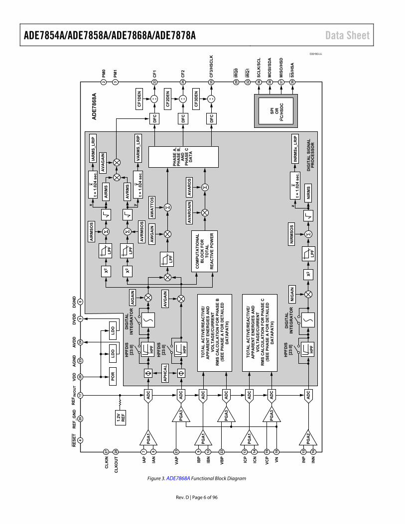
ADE7854AADE7858AADE7868AADE7878A Data Sheet
Rev D | Page 6 of 96
PG
A1
PG
A1
PG
A1
PG
A3
PG
A3
PG
A3
12V
RE
F
TO
TA
L A
CT
IVE
RE
AC
TIV
E
AP
PA
RE
NT
EN
ER
GIE
S A
ND
VO
LT
AG
EC
UR
RE
NT
RM
S C
AL
CU
LA
TIO
N F
OR
PH
AS
E B
(SE
E P
HA
SE
A F
OR
DE
TA
ILE
DD
AT
AP
AT
H)
TO
TA
L A
CT
IVE
RE
AC
TIV
E
AP
PA
RE
NT
EN
ER
GIE
S A
ND
VO
LT
AG
EC
UR
RE
NT
RM
S C
AL
CU
LA
TIO
N F
OR
PH
AS
E C
(SE
E P
HA
SE
A F
OR
DE
TA
ILE
DD
AT
AP
AT
H)
DIG
ITA
L S
IGN
AL
PR
OC
ES
SO
R
CO
MP
UT
AT
ION
AL
BL
OC
K F
OR
TO
TA
LR
EA
CT
IVE
PO
WE
R
AP
HC
AL
HP
FD
IS[2
30]
HP
F
HP
FD
IS[2
30]
HP
F
HP
FD
IS[2
30]
DIG
ITA
LIN
TE
GR
AT
OR
HP
F
DIG
ITA
LIN
TE
GR
AT
OR
PO
RL
DO
LD
O
X2
AIR
MS
LP
F
AIR
MS
OS
X2
X2
AV
RM
SL
PF
LP
F
AV
RM
SO
S
AV
AG
AIN
LP
F
AW
GA
IN
NIR
MS
NIR
MS
OS
AW
AT
TO
S
AV
AR
GA
INA
VA
RO
S
DF
C
CF
1DE
N
DF
C
CF
2DE
N
DF
C
CF
3DE
N
524
2625
174
7 8 9 2212 13 14 19 18
3937383632293534333227 28 23
6
RE
SE
TR
EF
INO
UT
VD
DA
GN
DA
VD
DD
VD
DD
GN
D
CL
KIN
CL
KO
UT
IAP
IAN
VA
P
IBP
IBN
VB
P
ICP
ICN
VC
P
VN
PM
0
PM
1
CF
1
CF
2
CF
3H
SC
LK
IRQ
0
IRQ
1
SC
LK
SC
L
MO
SI
SD
A
MIS
OH
SD
SS
HS
A
AD
E7
86
8A
AD
C
AD
C
AD
C
AD
C
AD
C
AD
C
PG
A2
15 16
INP
INN
AD
C
PH
AS
E A
P
HA
SE
B
AN
DP
HA
SE
CD
AT
A
SP
IO
RI2
CH
SD
C
NIG
AIN
AIG
AIN
AV
GA
IN
11136-003
20
RE
F_G
ND
yt
= 1
024
sec
IAR
MS
_LR
IP
VA
RM
S_L
RIP
yxx
t =
10
24 s
ec
INR
MS
x_L
RIP
zz
t =
10
24 s
ec
Figure 3 ADE7868A Functional Block Diagram
Data Sheet ADE7854AADE7858AADE7868AADE7878A
Rev D | Page 7 of 96
PG
A1
PG
A1
PG
A1
PG
A3
PG
A3
PG
A3
12V
RE
F
TO
TA
LF
UN
DA
ME
NT
AL
AC
TIV
E
RE
AC
TIV
E E
NE
RG
IES
A
PP
AR
EN
TE
NE
RG
Y A
ND
VO
LT
AG
EC
UR
RE
NT
RM
S C
AL
CU
LA
TIO
N F
OR
PH
AS
E B
(SE
E P
HA
SE
A F
OR
DE
TA
ILE
DD
AT
AP
AT
H)
TO
TA
LF
UN
DA
ME
NT
AL
AC
TIV
E
RE
AC
TIV
E E
NE
RG
IES
A
PP
AR
EN
TE
NE
RG
Y A
ND
VO
LT
AG
EC
UR
RE
NT
RM
S C
AL
CU
LA
TIO
N F
OR
PH
AS
E C
(SE
E P
HA
SE
A F
OR
DE
TA
ILE
DD
AT
AP
AT
H)
CO
MP
UT
AT
ION
AL
BL
OC
K F
OR
TO
TA
LR
EA
CT
IVE
PO
WE
R
AP
HC
AL
HP
FD
IS[2
30]
HP
F
HP
FD
IS[2
30]
HP
F
HP
FD
IS[2
30]
DIG
ITA
LIN
TE
GR
AT
OR
HP
F
DIG
ITA
LIN
TE
GR
AT
OR
PO
RL
DO
LD
O
X2
AIR
MS
LP
F
AIR
MS
OS
X2
X2
AV
RM
SL
PF
LP
F
AV
RM
SO
S
AV
AG
AIN
LP
F
CO
MP
UT
AT
ION
AL
BL
OC
K F
OR
FU
ND
AM
EN
TA
LA
CT
IVE
AN
DR
EA
CT
IVE
PO
WE
R
AW
GA
IN
NIR
MS
NIR
MS
OS
AW
AT
TO
S
AV
AR
GA
INA
VA
RO
S
AF
WG
AIN
AF
WA
TT
OS
AF
VA
RG
AIN
AF
VA
RO
S
PH
AS
E A
P
HA
SE
B
AN
DP
HA
SE
CD
AT
A
DF
C
CF
1DE
N
DF
C
CF
2DE
N
DF
C
CF
3DE
N
524
26
2517
4
7 8 9 2212 13 14 19 18
3937383632293534333227 28 23
6
RE
SE
TR
EF
INO
UT
VD
DA
GN
DA
VD
DD
VD
DD
GN
D
CL
KIN
CL
KO
UT
IAP
IAN
VA
P
IBP
IBN
VB
P
ICP
ICN
VC
P
VN
PM
0
PM
1
CF
1
CF
2
CF
3H
SC
LK
IRQ
0
IRQ
1
SC
LK
SC
L
MO
SI
SD
A
MIS
OH
SD
SS
HS
A
AD
E7
87
8A
AD
C
AD
C
AD
C
AD
C
AD
C
AD
C
PG
A2
15 16
INP
INN
AD
C
SP
IO
RI2
CH
SD
C
AV
GA
IN
NIG
AIN
AIG
AIN
11136-004
20
RE
F_G
ND
yt
= 1
024
sec
IAR
MS
_LR
IP
VA
RM
S_L
RIP
yxx
t =
10
24 s
ec D
IGIT
AL
SIG
NA
LP
RO
CE
SS
OR
INR
MS
x_L
RIP
zz
t =
10
24 s
ec
Figure 4 ADE7878A Functional Block Diagram
ADE7854AADE7858AADE7868AADE7878A Data Sheet
Rev D | Page 8 of 96
SPECIFICATIONS VDD = 33 V plusmn 10 AGND = DGND = 0 V on-chip reference CLKIN = 16384 MHz TMIN to TMAX = minus40degC to +85degC TTYP = 25degC unless otherwise noted
Table 2 Parameter1 2 3 Min Typ Max Unit Test ConditionsComments ACTIVE ENERGY MEASUREMENT (PSM0 MODE)
Active Energy Measurement Error (Per Phase) Total Active Energy 01 Over a dynamic range of 1000 to 1
PGA = 1 2 4 integrator off 02 Over a dynamic range of 3000 to 1
PGA = 1 2 4 integrator off 01 Over a dynamic range of 500 to 1
PGA = 8 16 integrator on Fundamental Active Energy ADE7878A only 01 Over a dynamic range of 1000 to 1
PGA = 1 2 4 integrator off 02 Over a dynamic range of 3000 to 1
PGA = 1 2 4 integrator off 01 Over a dynamic range of 500 to 1
PGA = 8 16 integrator on AC Power Supply Rejection VDD = 33 V + 120 mV rms at 120 Hz100 Hz
IxP = VxP = plusmn100 mV rms Output Frequency Variation 001
DC Power Supply Rejection VDD = 33 V plusmn 330 mV dc IxP = VxP = plusmn100 mV rms
Output Frequency Variation 001 Total Active Energy Measurement Bandwidth 2 kHz
REACTIVE ENERGY MEASUREMENT (PSM0 MODE) ADE7858A ADE7868A and ADE7878A Reactive Energy Measurement Error (Per Phase)
Total Reactive Energy 01 Over a dynamic range of 1000 to 1 PGA = 1 2 4 integrator off
02 Over a dynamic range of 3000 to 1 PGA = 1 2 4 integrator off
01 Over a dynamic range of 500 to 1 PGA = 8 16 integrator on
Fundamental Reactive Energy ADE7878A only 01 Over a dynamic range of 1000 to 1
PGA = 1 2 4 integrator off 02 Over a dynamic range of 3000 to 1
PGA = 1 2 4 integrator off 01 Over a dynamic range of 500 to 1
PGA = 8 16 integrator on AC Power Supply Rejection VDD = 33 V + 120 mV rms at 120 Hz100 Hz
IxP = VxP = plusmn100 mV rms Output Frequency Variation 001
DC Power Supply Rejection VDD = 33 V plusmn 330 mV dc IxP = VxP = plusmn100 mV rms
Output Frequency Variation 001 Total Reactive Energy Measurement Bandwidth 2 kHz
RMS MEASUREMENTS (PSM0 MODE) Current (I) RMS and Voltage (V) RMS
Measurement Bandwidth 2 kHz
I RMS and V RMS Measurement Error 01 Over a dynamic range of 1000 to 1 PGA = 1
MEAN ABSOLUTE VALUE (MAV) MEASUREMENT (PSM1 Mode)
ADE7868A and ADE7878A
I MAV Measurement Bandwidth 260 Hz I MAV Measurement Error 05 Over a dynamic range of 100 to 1 PGA = 1 2
4 8
Data Sheet ADE7854AADE7858AADE7868AADE7878A
Rev D | Page 9 of 96
Parameter1 2 3 Min Typ Max Unit Test ConditionsComments ANALOG INPUTS
Maximum Signal Levels plusmn500 mV peak PGA = 1 differential or single-ended inputs between the following pins IAP and IAN IBP and IBN ICP and ICN INP and INN single-ended inputs between the following pins VAP and VN VBP and VN VCP and VN
Input Impedance (DC) IAP IAN IBP IBN ICP ICN INP INN VAP
VBP and VCP Pins 400 kΩ
VN Pin 130 kΩ ADC Offset minus34 mV PGA = 1 see the Terminology section Gain Error plusmn4 External 12 V reference
WAVEFORM SAMPLING Sampling CLKIN2048 16384 MHz2048 = 8 kSPS
Current and Voltage Channels See the Waveform Sampling Mode section Signal-to-Noise Ratio SNR 74 dB PGA = 1 fundamental frequency = 45 Hz to
65 Hz see the Terminology section Signal-to-Noise-and-Distortion (SINAD)
Ratio 74 dB PGA = 1 fundamental frequency = 45 Hz to
65 Hz see the Terminology section Bandwidth (minus3 dB) 2 kHz
TIME INTERVAL BETWEEN PHASES Measurement Error 03 Degrees Line frequency = 45 Hz to 65 Hz HPF on
CF1 CF2 CF3 PULSE OUTPUTS Maximum Output Frequency 8 kHz WTHR = VARTHR = VATHR = PMAX =
33516139 Duty Cycle 50 CF1 CF2 or CF3 frequency gt 625 Hz CFDEN
is even and gt 1 (1 + 1CFDEN)
times 50 CF1 CF2 or CF3 frequency gt 625 Hz CFDEN
is odd and gt 1 Active Low Pulse Width 80 ms CF1 CF2 or CF3 frequency lt 625 Hz Jitter 004 CF1 CF2 or CF3 frequency = 1 Hz nominal
phase currents larger than 10 of full scale
REFERENCE INPUT REFINOUT Input Voltage Range 11 13 V Minimum = 12 V minus 8 maximum = 12 V + 8 Input Capacitance 10 pF
ON-CHIP REFERENCE PSM0 AND PSM1 MODES Nominal 12 V at the REFINOUT pin at TA = 25degC Temperature Coefficient minus32 plusmn5 +32 ppmdegC Drift across the entire temperature range of
minus40degC to +85degC is calculated with reference to 25degC see the Reference Circuit section
CLKIN CLKIN = 16384 MHz see the Crystal Circuit section
Input Clock Frequency 1622 16384 1655 MHz
LOGIC INPUTSmdashMOSISDA SCLKSCL SSHSA RESET PM0 AND PM1
Input High Voltage VINH 20 V VDD = 33 V plusmn 10 Input Low Voltage VINL 08 V VDD = 33 V plusmn 10 Input Current IIN minus87 μA Input = 0 V VDD = 33 V
3 μA Input = VDD = 33 V Input Capacitance CIN 10 pF
LOGIC OUTPUTS IRQ0 IRQ1 MISOHSD
Output High Voltage VOH 24 V VDD = 33 V plusmn 10 ISOURCE 800 μA
Output Low Voltage VOL 04 V VDD = 33 V plusmn 10 ISINK 2 mA
ADE7854AADE7858AADE7868AADE7878A Data Sheet
Rev D | Page 10 of 96
Parameter1 2 3 Min Typ Max Unit Test ConditionsComments CF1 CF2 CF3HSCLK
Output High Voltage VOH 24 V VDD = 33 V plusmn 10 ISOURCE 500 μA
Output Low Voltage VOL 04 V VDD = 33 V plusmn 10 ISINK 8 mA
POWER SUPPLY For specified performance PSM0 Mode
VDD Pin 297 363 V Minimum = 33 V minus 10 maximum = 33 V + 10
IDD 20 23 mA PSM1 and PSM2 Modes ADE7868A and ADE7878A
VDD Pin 28 37 V IDD
PSM1 Mode 45 mA PSM2 Mode 02 mA
PSM3 Mode VDD Pin 28 37 V IDD 17 μA
1 See the Typical Performance Characteristics section 2 See the Terminology section for a definition of the parameters 3 Note that dual function pin names are referenced by the relevant function only (see the Pin Configuration and Function Descriptions section for full pin mnemonics
and descriptions)
Data Sheet ADE7854AADE7858AADE7868AADE7878A
Rev D | Page 11 of 96
TIMING CHARACTERISTICS VDD = 33 V plusmn 10 AGND = DGND = 0 V on-chip reference CLKIN = 16384 MHz TMIN to TMAX = minus40degC to +85degC Note that within the timing tables and diagrams dual function pin names are referenced by the relevant function only (see the Pin Configuration and Function Descriptions section for full pin mnemonics and descriptions)
I2C Interface Timing
Table 3 Standard Mode Fast Mode Parameter Symbol Min Max Min Max Unit SCL Clock Frequency fSCL 0 100 0 400 kHz Hold Time for Start and Repeated Start Conditions tHDSTA 40 06 μs Low Period of SCL Clock tLOW 47 13 μs High Period of SCL Clock tHIGH 40 06 μs Setup Time for Repeated Start Condition tSUSTA 47 06 μs Data Hold Time tHDDAT 0 345 0 09 μs Data Setup Time tSUDAT 250 100 ns Rise Time of SDA and SCL Signals tR 1000 20 300 ns Fall Time of SDA and SCL Signals tF 300 20 300 ns Setup Time for Stop Condition tSUSTO 40 06 μs Bus Free Time Between a Stop and Start Condition tBUF 47 13 μs Pulse Width of Suppressed Spikes tSP NA1 50 ns 1 NA means not applicable
tF
tR
tHDDAT
tHDSTA
tHIGHtSUSTA
tSUDAT
tF
tHDSTA tSP
tSUSTO
tRtBUF
tLOW
SDA
SCL
STARTCONDITION
REPEATED STARTCONDITION
STOPCONDITION
STARTCONDITION 11
13
6-0
05
Figure 5 I2C Interface Timing
ADE7854AADE7858AADE7868AADE7878A Data Sheet
Rev D | Page 12 of 96
SPI Interface Timing
Table 4 Parameter Symbol Min Max Unit SS to SCLK Edge tSS 50 ns
SCLK Period 04 40001 μs SCLK Low Pulse Width tSL 175 ns SCLK High Pulse Width tSH 175 ns Data Output Valid After SCLK Edge tDAV 100 ns Data Input Setup Time Before SCLK Edge tDSU 100 ns Data Input Hold Time After SCLK Edge tDHD 5 ns Data Output Fall Time tDF 20 ns Data Output Rise Time tDR 20 ns SCLK Rise Time tSR 20 ns SCLK Fall Time tSF 20 ns MISO Disable After SS Rising Edge tDIS 200 ns
SS High After SCLK Edge tSFS 0 ns 1 Guaranteed by design
MSB LSB
LSB IN
INTERMEDIATE BITS
INTERMEDIATE BITS
tSFS
tDIS
tSS
tSL
tDF
tSH
tDHD
tDAV
tDSU
tSRtSF
tDR
MSB INMOSI
MISO
SCLK
SS
111
36-
00
6
Figure 6 SPI Interface Timing
Data Sheet ADE7854AADE7858AADE7868AADE7878A
Rev D | Page 13 of 96
HSDC Interface Timing
Table 5 Parameter Symbol Min Max Unit HSA to HSCLK Edge tSS 0 ns HSCLK Period 125 ns HSCLK Low Pulse Width tSL 50 ns HSCLK High Pulse Width tSH 50 ns Data Output Valid After HSCLK Edge tDAV 40 ns Data Output Fall Time tDF 20 ns Data Output Rise Time tDR 20 ns HSCLK Rise Time tSR 10 ns HSCLK Fall Time tSF 10 ns HSD Disable After HSA Rising Edge tDIS 5 ns HSA High After HSCLK Edge tSFS 0 ns
MSB LSBINTERMEDIATE BITS
tSFS
tDIS
tSS
tSL
tDF
tSHtDAVtSRtSF
tDR
HSD
HSCLK
HSA
111
36-0
07
Figure 7 HSDC Interface Timing
Load Circuit for Timing Specifications
2mA IOL
800microA IOH
16VTO OUTPUTPIN
CL50pF
111
36
-00
8
Figure 8 Load Circuit for Timing Specifications
ADE7854AADE7858AADE7868AADE7878A Data Sheet
Rev D | Page 14 of 96
ABSOLUTE MAXIMUM RATINGS TA = 25degC unless otherwise noted
Table 6 Parameter Rating VDD to AGND minus03 V to +37 V VDD to DGND minus03 V to +37 V Analog Input Voltage to AGND IAP IAN
IBP IBN ICP ICN VAP VBP VCP VN minus2 V to +2 V
Analog Input Voltage to INP and INN minus2 V to +2 V Reference Input Voltage to AGND minus03 V to VDD + 03 V Digital Input Voltage to DGND minus03 V to VDD + 03 V Digital Output Voltage to DGND minus03 V to VDD + 03 V Operating Temperature
Industrial Range minus40degC to +85degC Storage Temperature Range minus65degC to +150degC
Lead Temperature (Soldering 10 sec) 300degC
Stresses at or above those listed under Absolute Maximum Ratings may cause permanent damage to the product This is a stress rating only functional operation of the product at these or any other conditions above those indicated in the operational section of this specification is not implied Operation beyond the maximum operating conditions for extended periods may affect product reliability
THERMAL RESISTANCE θJA is specified at 293degCW θJC is specified at 18degCW
Table 7 Thermal Resistance Package Type θJA θJC Unit 40-Lead LFCSP 293 18 degCW
ESD CAUTION
Data Sheet ADE7854AADE7858AADE7868AADE7878A
Rev D | Page 15 of 96
PIN CONFIGURATION AND FUNCTION DESCRIPTIONS
NOTES1 NC = NO CONNECT THESE PINS ARE NOT CONNECTED INTERNALLY IT IS RECOMMENDED THAT THESE PINS BE GROUNDED
2 CREATE A SIMILAR PAD ON THE PCB UNDER THE EXPOSED PAD SOLDER THE EXPOSED PAD TO THE PAD ON THE PCB TO CONFER MECHANICAL STRENGTH TO THE PACKAGE CONNECT THE PADS TO AGND AND DGND
11N
C12
IBN
13IC
P
15IN
P
17R
EF
INO
UT
16IN
N
18V
N19
VC
P20
RE
F_G
ND
14IC
N
NCPM0PM1
RESETDVDDDGND
IAPIANIBPNC
VAPAVDDAGNDVDDCLKINCLKOUTIRQ0NC
VBPNC
33C
F1
CF
235 34
CF
3H
SC
LK
36S
CL
KS
CL
37M
ISO
HS
D38
MO
SI
SD
A39
SS
HS
A40
NC
32IR
Q1
31N
C
123456789
10
2324252627282930
2221
ADE7854AADE7858AADE7868AADE7878A
TOP VIEW(Not to Scale)
111
36-
00
9
Figure 9 Pin Configuration
Table 8 Pin Function Descriptions Pin No Mnemonic Description 1 10 11 21 30 31 40
NC No Connect These pins are not connected internally It is recommended that these pins be grounded
2 PM0 Power Mode Pin 0 The PM0 and PM1 pins together specify the power mode of the ADE7854A ADE7858A ADE7868A and ADE7878A (see Table 9)
3 PM1 Power Mode Pin 1 The PM1 and PM0 pins together specify the power mode of the ADE7854A ADE7858A ADE7868A and ADE7878A (see Table 9)
4 RESET Reset Input Active Low In PSM0 mode this pin must stay low for at least 10 μs to trigger a hardware reset
5 DVDD 25 V Output of the Digital Low Dropout (LDO) Regulator Decouple this pin with a 47 μF capacitor in parallel with a ceramic 220 nF capacitor Do not connect external active circuitry to this pin
6 DGND Ground Reference for the Digital Circuitry 7 8 IAP IAN Analog Inputs Current Channel A Current Channel A is used with the current transducers The IAP (positive)
and IAN (negative) inputs are fully differential voltage inputs with a maximum differential level of plusmn05 V peak Channel A also has an internal PGA which is set to the same value as the PGAs used by Channel B and Channel C
9 12 IBP IBN Analog Inputs Current Channel B Current Channel B is used with the current transducers The IBP (positive) and IBN (negative) inputs are fully differential voltage inputs with a maximum differential level of plusmn05 V peak Channel B also has an internal PGA which is set to the same value as the PGAs used by Channel A and Channel C
13 14 ICP ICN Analog Inputs Current Channel C Current Channel C is used with the current transducers The ICP (positive) and ICN (negative) inputs are fully differential voltage inputs with a maximum differential level of plusmn05 V peak Channel C also has an internal PGA which is set to the same value as the PGAs used by Channel A and Channel B
15 16 INP INN Analog Inputs Neutral Current Channel N Current Channel N is used with the current transducers The INP (positive) and INN (negative) inputs are fully differential voltage inputs with a maximum differential level of plusmn05 V peak Channel N also has an internal PGA which is separate from the PGA used by Channel A Channel B and Channel C The neutral current channel is available in the ADE7868A and ADE7878A only In the ADE7854A and ADE7858A connect the INP and INN pins to AGND
17 REFINOUT The REFINOUT pin provides access to the on-chip voltage reference The on-chip reference has a nominal value of 12 V An external reference source with 12 V plusmn 8 can also be connected at this pin In either case decouple REFINOUT to AGND with a 47 μF capacitor in parallel with a ceramic 100 nF capacitor After a reset the on-chip reference is enabled
ADE7854AADE7858AADE7868AADE7878A Data Sheet
Rev D | Page 16 of 96
Pin No Mnemonic Description 18 19 22 23 VN VCP VBP
VAP Analog Inputs Voltage Channels These channels are used with the voltage transducer The VN VCP VBP and VAP inputs are single-ended voltage inputs with a maximum signal level of plusmn05 V peak with respect to VN for specified operation Each voltage channel also has an internal PGA
20 REF_GND Ground Reference Internal Voltage Reference Connect REF_GND to the analog ground plane 24 AVDD 25 V Output of the Analog Low Dropout (LDO) Regulator Decouple this pin with a 47 μF capacitor in
parallel with a ceramic 220 nF capacitor Do not connect external active circuitry to this pin 25 AGND Ground Reference for the Analog Circuitry Tie AGND to the analog ground plane or to the quietest ground
reference in the system Use this quiet ground reference for all analog circuitry for example antialiasing filters current transducers and voltage transducers
26 VDD Supply Voltage The VDD pin provides the supply voltage In PSM0 (normal power) mode maintain the supply voltage at 33 V plusmn 10 for specified operation In PSM1 (reduced power) mode PSM2 (low power) mode and PSM3 (sleep) mode when the ADE7868A or ADE7878A is supplied from a battery maintain the supply voltage from 28 V to 37 V Decouple VDD to AGND with a 10 μF capacitor in parallel with a ceramic 100 nF capacitor The only power modes available on the ADE7858A and ADE7854A are the PSM0 and PSM3 modes
27 CLKIN Master Clock An external clock can be provided at this logic input Alternatively a crystal can be connected across the CLKIN and CLKOUT pins to provide a clock source for the ADE7854A ADE7858A ADE7868A or ADE7878A The clock frequency for specified operation is 16384 MHz For information about choosing a suitable crystal see the Crystal Circuit section
28 CLKOUT Crystal Output A crystal can be connected across the CLKIN and CLKOUT pins to provide a clock source for the ADE7854A ADE7858A ADE7868A or ADE7878A The clock frequency for specified operation is 16384 MHz For information about choosing a suitable crystal see the Crystal Circuit section
29 32 IRQ0 IRQ1 Interrupt Request Outputs These pins are active low logic outputs For information about events that trigger interrupts see the Interrupts section
33 34 35 CF1 CF2 CF3HSCLK
Calibration Frequency Logic OutputsSerial Clock Output of the HSDC Port The CF1 CF2 and CF3HSCLK outputs provide power information based on the CF1SEL[20] CF2SEL[20] and CF3SEL[20] bits in the CFMODE register Use these outputs for operational and calibration purposes Scale the full-scale output frequency by writing to the CF1DEN CF2DEN and CF3DEN registers (see the Energy to Frequency Conversion section) CF3 is multiplexed with HSCLK
36 SCLKSCL Serial Clock Input for the SPI PortSerial Clock Input for the I2C Port All serial data transfers synchronize to this clock (see the Serial Interfaces section) The SCLKSCL pin has a Schmitt trigger input for use with a clock source that has a slow edge transition time for example opto-isolator outputs
37 MISOHSD Data Output for the SPI PortData Output for the HSDC Port 38 MOSISDA Data Input for the SPI PortData Input and Output for the I2C Port 39 SSHSA Slave Select for the SPI PortHSDC Port Active
EP Exposed Pad Create a similar pad on the printed circuit board (PCB) under the exposed pad Solder the exposed pad to the pad on the PCB to confer mechanical strength to the package Connect the pads to AGND and DGND
Data Sheet ADE7854AADE7858AADE7868AADE7878A
Rev D | Page 17 of 96
TYPICAL PERFORMANCE CHARACTERISTICS
001 01 1 10 100
ER
RO
R (
)
PERCENTAGE OF FULL-SCALE CURRENT ()
ndash40degC+25degC+85degC
111
36-1
10
VDD = 33V
ndash06
ndash05
ndash04
ndash03
ndash02
ndash01
0
01
02
03
04
05
06
Figure 10 Total Active Energy Error as a Percentage of Reading (Gain = +1 Power Factor = 1) vs Percentage of Full-Scale Current over Temperature with Internal
Reference and Integrator Off
ndash015
ndash012
ndash009
ndash006
ndash003
0
003
006
009
012
015
ER
RO
R (
)
LINE FREQUENCY (Hz) 111
36-
111
40 45 50 55 60 65 70
PF = 1PF = 05PF = ndash05
Figure 11 Total Active Energy Error as a Percentage of Reading (Gain = +1) vs Line Frequency over Power Factor with Internal Reference and Integrator Off
1113
6-1
12001 01 1 10 100
ER
RO
R (
)
PERCENTAGE OF FULL-SCALE CURRENT ()
ndash06
ndash05
ndash04
ndash03
ndash02
ndash01
0
01
02
03
04
05
06297V330V363V
TA = 25degC
Figure 12 Total Active Energy Error as a Percentage of Reading (Gain = +1 Power Factor = 1) vs Percentage of Full-Scale Current over Power Supply with Internal
Reference and Integrator Off
01 1 10 100
PERCENTAGE OF FULL-SCALE CURRENT ()
ndash40degC+25degC+85degC
111
36
-11
3
VDD = 33V
ER
RO
R (
)
ndash06
ndash05
ndash04
ndash03
ndash02
ndash01
0
01
02
03
04
05
06
Figure 13 Total Active Energy Error as a Percentage of Reading (Gain = +16 Power Factor = 1) vs Percentage of Full-Scale Current over Temperature with
Internal Reference and Integrator On
ER
RO
R (
)
ndash06
ndash05
ndash04
ndash03
ndash02
ndash01
0
01
02
03
04
05
06
01 1 10 100
PERCENTAGE OF FULL-SCALE CURRENT ()
ndash40degC+25degC+85degC
111
36-
114
VDD = 33V
Figure 14 Total Reactive Energy Error as a Percentage of Reading (Gain = +1 Power Factor = 0) vs Percentage of Full-Scale Current over Temperature with
Internal Reference and Integrator Off
LINE FREQUENCY (Hz)
PF ndash0866PF 0PF 0866
1113
6-1
15ndash015
ndash012
ndash009
ndash006
ndash003
003
0
006
009
012
015
ER
RO
R (
)
40 45 50 55 60 65 70
Figure 15 Total Reactive Energy Error as a Percentage of Reading (Gain = +1) vs Line Frequency over Power Factor with Internal Reference and
Integrator Off
ADE7854AADE7858AADE7868AADE7878A Data Sheet
Rev D | Page 18 of 96
001 01 1 10 100
PERCENTAGE OF FULL-SCALE CURRENT ()
297V330V363V
TA = 25degC
111
36-
116
ER
RO
R (
)
ndash06
ndash05
ndash04
ndash03
ndash02
ndash01
0
01
02
03
04
05
06
Figure 16 Total Reactive Energy Error as a Percentage of Reading (Gain = +1 Power Factor = 0) vs Percentage of Full-Scale Current over Power Supply with
Internal Reference and Integrator Off
ER
RO
R (
)
ndash06
ndash05
ndash04
ndash03
ndash02
ndash01
0
01
02
03
04
05
06
01 1 10 100
PERCENTAGE OF FULL-SCALE CURRENT ()
ndash40degC+25degC+85degC
111
36-1
17
VDD = 33V
Figure 17 Total Reactive Energy Error as a Percentage of Reading (Gain = +16 Power Factor = 0) vs Percentage of Full-Scale Current over Temperature with
Internal Reference and Integrator On
111
36-1
18ndash015
ndash012
ndash009
ndash006
ndash003
0
003
006
009
012
015
40 45 50 55 60 65 70
ER
RO
R (
)
LINE FREQUENCY (Hz)
PF = 1PF = 05PF = ndash05
Figure 18 Fundamental Active Energy Error as a Percentage of Reading (Gain = +1) vs Line Frequency over Power Factor over Frequency with Internal
Reference and Integrator Off
01 1 10 100
ER
RO
R (
)
PERCENTAGE OF FULL-SCALE CURRENT ()
ndash40degC+25degC+85degC
111
36-1
19
VDD = 33V
ndash06
ndash05
ndash04
ndash03
ndash02
ndash01
0
01
02
03
04
05
06
Figure 19 Fundamental Active Energy Error as a Percentage of Reading (Gain = +16) vs Percentage of Full-Scale Current over Temperature with
Internal Reference and Integrator On
LINE FREQUENCY (Hz)
PF ndash0866PF 0PF 0866
111
36
-12
0ndash015
ndash012
ndash009
ndash006
ndash003
003
0
006
009
012
015
ER
RO
R (
)
40 45 50 55 60 65 70
Figure 20 Fundamental Reactive Energy Error as a Percentage of Reading (Gain = +1) vs Line Frequency over Power Factor with Internal Reference and
Integrator Off
ER
RO
R (
)
ndash06
ndash05
ndash04
ndash03
ndash02
ndash01
0
01
02
03
04
05
06
01 1 10 100
PERCENTAGE OF FULL-SCALE CURRENT ()
ndash40degC+25degC+85degC
111
36-1
21
VDD = 33V
Figure 21 Fundamental Reactive Energy Error as a Percentage of Reading (Gain = +16) vs Percentage of Full-Scale Current over Temperature with
Internal Reference and Integrator On
Data Sheet ADE7854AADE7858AADE7868AADE7878A
Rev D | Page 19 of 96
ER
RO
R (
)
ndash06
ndash05
ndash04
ndash03
ndash02
ndash01
0
01
02
03
04
05
06
01 1 10 100
PERCENTAGE OF FULL-SCALE CURRENT ()
ndash40degC+25degC+85degC
111
36-2
02
VDD = 33V
Figure 22 I RMS Error as a Percentage of Reading (Gain = +1 Power Factor = 1) vs Percentage of Full-Scale Current over Temperature with Internal Reference
and Integrator Off
ADE7854AADE7858AADE7868AADE7878A Data Sheet
Rev D | Page 20 of 96
TEST CIRCUIT In Figure 23 the PM1 and PM0 pins are pulled up internally to VDD Select the mode of operation by using a microcontroller to programmatically change the pin values (see the Power Management section)
SAME ASCF2
PM0
022microF47microF
MOSISDA
MISOHSD
SCLKSCL
CF3HSCLK
CF2
CF1
REFINOUT
CLKOUT
CLKIN
PM1
RESET
IAP
IAN
IBP
IBN
ICP
ICN
VN
VCP
VBP
VAP
2
23
3
4
7
8
9
12
13
14
18
19
22
39
38
37
36
35
34
33
32
29
17
28
27
ADE78xxA
24 26 5
AV
DD
VD
D
DV
DD
6
DG
ND
25
AG
ND
1
NC
10
NC
11
NC
21
NC
30
NC
31
NC
40
NC
EP
EP
AD
20
RE
F_G
ND
022microF47microF
01microF47microF+
+ +
01microF10microF+
CL2
CL1
16384MHz
SAME ASVCP
SAME ASVCP
SAME ASIAP IAN
SAME ASIAP IAN
22nF1kΩ
1kΩ
1kΩ10kΩ 15kΩ
1kΩ 22nF
33V
33V
33V
1microF
22nF
22nF
SSHSA
IRQ1
IRQ0
1113
6-0
15
Figure 23 Test Circuit
Data Sheet ADE7854AADE7858AADE7868AADE7878A
Rev D | Page 21 of 96
TERMINOLOGY Measurement Error The error associated with the energy measurement made by the ADE7854AADE7858AADE7868AADE7878A is defined as follows
Measurement Error =
100
EnergyTrueEnergyTrue DevicebyRegisteredEnergy
(1)
where Device represents the ADE7854A ADE7858A ADE7868A or ADE7878A
Power Supply Rejection (PSR) PSR quantifies the ADE7854AADE7858AADE7868A ADE7878A measurement error as a percentage of reading when the power supplies are varied For the ac PSR measurement a reading at nominal supplies (33 V) is taken A second reading is obtained with the same input signal levels when an ac signal (120 mV rms at twice the fundamental frequency) is introduced onto the supplies Any error introduced by this ac signal is expressed as a percentage of reading
For the dc PSR measurement a reading at nominal supplies (33 V) is taken A second reading is obtained with the same input signal levels when the power supplies are varied by plusmn10 Any error introduced is expressed as a percentage of the reading
ADC Offset ADC offset refers to the dc offset associated with the analog inputs to the ADCs It means that with the analog inputs connected to AGND the ADCs still see a dc analog input signal The magnitude of the offset depends on the gain and input range selection The high-pass filter (HPF) removes the offset from the current and voltage channels therefore the power calculation remains unaffected by this offset
Gain Error The gain error in the ADCs of the ADE7854AADE7858A ADE7868AADE7878A is defined as the difference between the measured ADC output code (minus the offset) and the ideal output code (see the Current Channel ADC and Voltage Channel ADC sections) The difference is expressed as a percentage of the ideal code
CF Jitter The period of pulses at one of the CF1 CF2 or CF3HSCLK pins is continuously measured The maximum minimum and average values of four consecutive pulses are computed as follows
Maximum = max(Period0 Period1 Period2 Period3)
Minimum = min(Period0 Period1 Period2 Period3)
Average = 4
3210 PeriodPeriodPeriodPeriod
The CF jitter is then computed as follows
100
Average
MinimumMaximumCFJITTER (2)
Signal-to-Noise Ratio (SNR) SNR is the ratio of the rms value of the actual input signal to the rms sum of all other spectral components below 2 kHz excluding harmonics and dc The input signal contains only the fundamental component The spectral components are calculated over a 2 sec window The value for SNR is expressed in decibels
Signal-to-Noise-and-Distortion (SINAD) Ratio SINAD is the ratio of the rms value of the actual input signal to the rms sum of all other spectral components below 2 kHz including harmonics but excluding dc The input signal contains only the fundamental component The spectral components are calculated over a 2 sec window The value for SINAD is expressed in decibels
ADE7854AADE7858AADE7868AADE7878A Data Sheet
Rev D | Page 22 of 96
POWER MANAGEMENT The ADE7868AADE7878A have four modes of operation and the ADE7854AADE7858A have two modes of operation the modes of operation are determined by the state of the PM0 and PM1 pins (see Table 9)
Table 9 Power Supply Modes Power Supply Mode PM1 Pin PM0 Pin PSM0 Normal Power Mode 0 1 PSM1 Reduced Power Mode1 0 0 PSM2 Low Power Mode1 1 0 PSM3 Sleep Mode 1 1 1 Available in the ADE7868A and ADE7878A only
The PM1 and PM0 pins control the operation of the ADE7854A ADE7858AADE7868AADE7878A These pins are easily con-nected to an external microprocessor inputoutput The PM1 and PM0 pins include internal pull-up resistors therefore the ADE7854AADE7858AADE7868AADE7878A are in sleep mode by default For recommended actions to take before and after setting a new power mode see Table 11 and Table 12
PSM0 NORMAL POWER MODE (ALL DEVICES) In PSM0 normal power mode (PSM0 mode) the ADE7854A ADE7858AADE7868AADE7878A are fully functional To enter PSM0 mode the PM1 pin is set low and the PM0 pin is set high When a device is in PSM1 PSM2 or PSM3 mode and switches to PSM0 mode all control registers revert to their default values except for the threshold register LPOILVL (which is used in PSM2 mode) and the CONFIG2 register These registers maintain their programmed values
The ADE7854AADE7858AADE7868AADE7878A signal the completion of the power-up procedure by driving the IRQ1 interrupt pin low and setting Bit 15 (RSTDONE) in the STATUS1 register to 1 Bit 15 is cleared to 0 during the power-up sequence and is set to 1 when the chip enters PSM0 mode Writing to the STATUS1 register with the RSTDONE bit set to 1 clears the status bit and returns the IRQ1 pin high
The RSTDONE interrupt cannot be masked because Bit 15 (RSTDONE) in the interrupt mask register has no functionality
PSM1 REDUCED POWER MODE (ADE7868A AND ADE7878A ONLY) The PSM1 reduced power mode (PSM1 mode) is available on the ADE7868A and ADE7878A only In PSM1 mode the ADE7868AADE7878A measure the mean absolute values (MAV) of the 3-phase currents and store the results in the 20-bit AIMAV BIMAV and CIMAV registers PSM1 mode is useful in missing neutral cases where an external battery provides the voltage supply for the ADE7868A or ADE7878A
The I2C or SPI serial port is enabled in PSM1 mode and can be used to read the AIMAV BIMAV and CIMAV registers Do not read any other registers because their values are not guaranteed in PSM1 mode Similarly a write operation in PSM1 mode is ignored by the ADE7868AADE7878A In PSM1 mode do not access any registers other than AIMAV BIMAV and CIMAV For more information about the xIMAV registers see the Current Mean Absolute Value CalculationmdashADE7868A and ADE7878A Only section
The circuit that measures the estimates of rms values is also active during PSM0 mode therefore the calibration of this circuit can be done in either PSM0 mode or PSM1 mode Note that the ADE7868A and ADE7878A do not provide registers to store or process the corrections resulting from the calibration process The external microprocessor stores the gain values from these measurements and uses them during PSM1 mode
The 20-bit mean absolute value measurements that are completed in PSM1 mode are available in PSM0 mode However the MAV values are different from the rms measurements of phase currents and voltages that are executed only in PSM0 mode and stored in the xIRMS and xVRMS 24-bit registers For more information see the Current Mean Absolute Value CalculationmdashADE7868A and ADE7878A Only section
If the ADE7868AADE7878A are set to PSM1 mode while configured for PSM0 mode the devices immediately begin the mean absolute value calculations The xIMAV registers are accessible at any time however if the ADE7878A or ADE7868A is set to PSM1 mode while configured for PSM2 or PSM3 mode the ADE7868AADE7878A signal the start of the mean absolute value computations by driving the IRQ1 pin low The xIMAV registers can be accessed only after the IRQ1 pin is low
PSM2 LOW POWER MODE (ADE7868A AND ADE7878A ONLY) The PSM2 low power mode (PSM2 mode) is available on the ADE7868A and ADE7878A only PSM2 mode reduces the power consumption required to monitor the currents when there is no voltage input and an external battery provides the voltage supply for the ADE7868AADE7878A
PSM2 mode detects a missing neutral tamper condition by monitoring all phase currents and comparing them with a programmable threshold If any phase current rises above the programmable threshold for a programmable period the device assumes that a tamper attack has occurred If all currents remain below the programmable threshold no tamper attack has taken place instead a simple power outage has occurred
When a missing neutral tamper condition occurs the external microprocessor sets the ADE7868AADE7878A to PSM1 mode measures the mean absolute values of the phase currents and integrates the energy based on these values and the nominal voltage The I2C or SPI port is not functional during this mode
Data Sheet ADE7854AADE7858AADE7868AADE7878A
Rev D | Page 23 of 96
It is best practice to use the ADE7868AADE7878A in PSM2 mode when the PGA1 gain is 1 or 2 PGA1 represents the gain in the current channel datapath Do not use the ADE7868A or ADE7878A in PSM2 mode when the PGA1 gain is 4 8 or 16
Two PSM2 modes of operation are available PSM2 interrupt mode and PSM2 IRQ1 only mode The PSM2 interrupt mode is the default mode If the use of an external timer is possible use the PSM2 IRQ1 only mode
The PSM2 level threshold comparison is based on a peak detection methodology The peak detection circuit makes the comparison based on the positive terminal current channel input IAP IBP and ICP (see Figure 24) If differential inputs are applied to the current channels Figure 24 shows the differential antiphase signals at each current input terminal IxP and IxN and the net differential current IxP minus IxN
VREF
IxP
IxN
TAMPERINDICATION
+V p-p
ndashV p-p
ndashV p-p2
ndashV p-p2
+V p-p2
+V p-p2
PEAK DETECT CIRCUIT
IxP ndash IxN
IxP
(a)
(b) 111
36-2
03
Figure 24 PSM2 Low Power Mode Peak Detection
PSM2 Interrupt Mode (Default)
In PSM2 interrupt mode the ADE7868AADE7878A compare all phase currents against the programmable threshold for the programmable period of time During this time if one phase current exceeds the threshold a counter is incremented If a single phase counter is greater than or equal to LPLINE[40] + 1 at the end of the measurement period the IRQ1 pin is pulled low If every phase counter remains below LPLINE[40] + 1 at the end of the measurement period the IRQ0 pin is pulled low
In this way a combination of the IRQ0 and IRQ1 pins is used to determine the outcome of the measurement as follows
IRQ0 pulled low no tamper detected When the IRQ0 pin is pulled low at the end of a measurement period it indicates that all phase currents are below the defined threshold and therefore no current is flowing through the system In this case the device does not detect a tamper condition The external microprocessor sets the ADE7868AADE7878A to PSM3 sleep mode
IRQ1 pulled low missing neutral tamper condition detected When the IRQ1 pin is pulled low at the end of the measure-ment period it indicates that at least one current input is above the defined threshold and current is flowing through the system although no voltage is present at the ADE7868A ADE7878A pins This condition indicates the occurrence of a missing neutral tamper condition At this point the external microprocessor sets the ADE7868AADE7878A to PSM1 mode measures the mean absolute values of the phase currents and integrates the energy based on these values and the nominal voltage
Setting the Measurement Period
The measurement period is defined by Bits[73] (LPLINE[40]) of the LPOILVL register (Address 0xEC00) The measurement period is independent of the line frequency and is defined as
Measurement Period (sec) = 002 times (LPLINE[40] + 10)
Setting the Threshold
The threshold is defined by Bits[20] (LPOIL[20]) of the LPOILVL register (see Table 10) The threshold level is for signal levels with the PGA set to 1 When LPOIL[20] = 111 the absolute value of the threshold typically varies by up to plusmn30
Table 10 LPOILVL Register Bits Bit Name Value Description [20] LPOIL[20] Input signal levels that correspond
to the following thresholds 000 71 mV rms 001 Reserved 010 Reserved 011 1 mV rms 100 Reserved 101 Reserved 110 Reserved 111 0471 mV rms
[73] LPLINE[40] Default value is 00000 Measurement period in PSM2 interrupt mode is
002 times (LPLINE[40] + 10) sec Measurement period in PSM2 IRQ1 only mode is
002 times (LPLINE[40] + 1) sec
Figure 25 shows the typical variation around each threshold level the gray regions in Figure 25 indicate where the feature may not yield expected and uniform results The current levels outside this gray range help detect a tamper condition For example setting the threshold to 0471 mV rms provides dependable tamper detection results for current levels above 0707 mV rms and below 0353 mV rms
ADE7854AADE7858AADE7868AADE7878A Data Sheet
Rev D | Page 24 of 96
71mV rms79mV rms
RATIO TOFULL SCALE
64mV rms
1mV rms LPOIL[20] = 011
LPOIL[20] = 000
LPOIL[20] = 111
118mV rms
088mV rms
0471mV rms
0707mV rms
0353mV rms
111
36
-12
4
DETECTSTAMPERCONDITIONSABOVETHIS LEVEL
DETECTS NONTAMPERCONDITIONS
BELOWTHIS LEVEL
Figure 25 Variation Around Each Threshold Setting
Figure 26 shows the behavior of the ADE7868AADE7878A PSM2 mode when LPLINE[40] = 2 The test period is 12 cycles at 50 Hz (240 ms) the Phase A current rises above the LPOIL[20] threshold five times Because the counter value is above the internal counter requirement of LPLINE[40] + 1 the IRQ1 pin is pulled low at the end of the test period This result suggests that a missing neutral tamper condition has occurred
PSM2 IRQ1 Only Mode
The PSM2 IRQ1 only mode uses only the IRQ1 pin to indicate a tamper event If no tamper event has occurred no signal is provided by the ADE7868A or ADE7878A
To disable the IRQ0 pin and thus enable the PSM2 IRQ1 only mode set Bit 2 (IRQ0_DIS) in the CONFIG2 register (Address 0xEC01) to 1 Selecting this mode defines the recommended measurement period using the following formula
Recommended Measurement Period (sec) = 002 times (LPLINE[40] + 1)
Because a wait is required during this measurement period use an external timer before checking the status of the IRQ1 interrupt The measurement period can be longer than the recommended period because the internal phase counter continues to increment for the entire time that the device is in PSM2 mode Switching to PSM3 mode and then back to PSM2 mode causes the device to enter the PSM2 interrupt mode (the default PSM2 mode)
PSM3 SLEEP MODE (ALL DEVICES) PSM3 sleep mode is available on all devices ADE7854A ADE7858A ADE7868A and ADE7878A In sleep mode most of the internal circuits in the devices are turned off and the current consumption is at its lowest level When configuring the device for sleep mode set the RESET SCLKSCL MOSISDA and SSHSA pins high
In PSM3 sleep mode the I2C HSDC and SPI ports are not functional
LPLINE[40] = 2
MEASUREMENT PERIOD = 12 CYCLES (50Hz)
LPOIL[20]THRESHOLD
IA CURRENT
PH
AS
EC
OU
NT
ER
= 1
PH
AS
EC
OU
NT
ER
= 2
PH
AS
EC
OU
NT
ER
= 3
PH
AS
EC
OU
NT
ER
= 4
PH
AS
EC
OU
NT
ER
= 5
IRQ1
AS PHASE COUNTER gt LPLINE[40] +1 IRQ1 IS TRIGGERED
111
36-
016
Figure 26 PSM2 Interrupt Mode Triggering IRQ1 Pin for LPLINE[40] = 2 (50 Hz Systems)
Data Sheet ADE7854AADE7858AADE7868AADE7878A
Rev D | Page 25 of 96
Table 11 Power Modes and Related Characteristics
Power Mode LPOILVL and CONFIG2 Registers All Other Registers1 I2CSPI Port Functionality
PSM0 After Hardware Reset Set to default values Set to default values I2C port enabled All circuits are active and DSP is in
idle mode After Software Reset Unchanged Set to default values If the lock-in procedure was
previously executed the active serial port is unchanged
All circuits are active and DSP is in idle mode
PSM1 (ADE7868A and ADE7878A Only)
Values set during PSM0 mode are unchanged
Not available I2C or SPI port enabled but with limited functionality
Current mean absolute values are computed and the results are stored in the AIMAV BIMAV and CIMAV registers
PSM2 (ADE7868A and ADE7878A Only)
Values set during PSM0 mode are unchanged
Not available Serial port disabled Compares phase currents against the threshold set in the LPOILVL register and triggers the IRQ0 or IRQ1 pin accordingly
PSM3 Values set during PSM0 mode are unchanged
Not available Serial port disabled Internal circuits are shut down
1 Setting for all registers except the LPOILVL and CONFIG2 registers
Table 12 Recommended Actions When Changing Power Modes
Initial Power Mode
Recommended Actions Before Setting Next Power Mode
Next Power Mode
PSM0 PSM1 PSM2 PSM3 PSM0 Stop the DSP by setting
the run register to 0x0000
Current mean absolute values (MAV) computed immediately
Wait until the IRQ0 or IRQ1 pin is pulled low
No action necessary
Disable HSDC by clearing Bit 6 (HSDCEN) to 0 in the CONFIG register
xIMAV registers immediately accessible
Mask interrupts by setting MASK0 and MASK1 registers to 0x0
Erase interrupt status flags in the STATUS0 and STATUS1 registers
PSM1 (ADE7868A and ADE7878A Only)
No action necessary Wait until the IRQ1 pin is pulled low
Wait until the IRQ0 or IRQ1 pin is pulled low
No action necessary
Poll the STATUS1 register until Bit 15 (RSTDONE) is set to 1
PSM2 (ADE7868A and ADE7878A Only)
No action necessary Wait until the IRQ1 pin is pulled low
Wait until the IRQ1 pin is pulled low
No action necessary
Poll the STATUS1 register until Bit 15 (RSTDONE) is set to 1
Current mean absolute values computed after IRQ1 pin is pulled low
xIMAV registers accessible after IRQ1 pin is pulled low
PSM3 No action necessary Wait until the IRQ1 pin is pulled low
Wait until the IRQ1 pin is pulled low
Wait until the IRQ0 or IRQ1 pin is pulled low
Poll the STATUS1 register until Bit 15 (RSTDONE) is set to 1
Current mean absolute values computed after IRQ1 pin is pulled low
xIMAV registers accessible after IRQ1 pin is pulled low
ADE7854AADE7858AADE7868AADE7878A Data Sheet
Rev D | Page 26 of 96
POWER-UP PROCEDURE
POR TIMERTURNED ON
ADE78xxAFULLY
POWERED UP
MICROPROCESSORMAKES THECHOICE BETWEENI2C AND SPI
MICROPROCESSORSETS PM1 PIN TO 0APPLY VDD TO IC
RSTDONEINTERRUPTTRIGGERED
~40ms~26ms
0V
VD
D
33V ndash 10
25V plusmn 10 ADE78xxAPSM0 READY
111
36-
01
7
Figure 27 Power-Up Procedure
The ADE7854AADE7858AADE7868AADE7878A contain an on-chip power supply monitor that supervises the power supply (VDD) At power-up the device is inactive until VDD reaches 25 V plusmn 10 When VDD crosses this threshold the power supply monitor keeps the device in the inactive state for an additional 26 ms to allow VDD to rise to 33 V minus 10 the minimum recommended supply voltage
The PM0 and PM1 pins have internal pull-up resistors but it is necessary to set the PM1 pin to Logic 0 either through a microcontroller or by grounding the PM1 pin externally before powering up the chip The PM0 pin can remain open as it is held high due to the internal pull-up resistor This ensures that ADE7854AADE7858AADE7868AADE7878A always power up in PSM0 (normal) mode The time taken from the chip being powered up completely to the state where all functionality is enabled is about 40 ms (see Figure 27) It is necessary to ensure that the RESET pin is held high during the entire power-up procedure
If PSM0 mode is the only desired power mode the PM1 pin can be tied to ground externally When the ADE7854AADE7858A ADE7868AADE7878A enter PSM0 mode the I2C port is the active serial port To use the SPI port toggle the SSHSA pin three times from high to low
To lock I2C as the active serial port set Bit 1 (I2C_LOCK) of the CONFIG2 register to 1 From this moment the device ignores spurious toggling of the SSHSA pin and a switch to the SPI port is no longer possible
If SPI is the active serial port any write to the CONFIG2 register locks the port and a switch to the I2C port is no longer possible To use the I2C port the ADE7854AADE7858AADE7868A ADE7878A must be powered down or the device must be reset by setting the RESET pin low After the serial port is locked the serial port selection is maintained when the device changes from one PSMx power mode to another
Immediately after entering PSM0 mode all registers in the ADE7854AADE7858AADE7868AADE7878A are set to their default values including the CONFIG2 and LPOILVL registers
The ADE7854AADE7858AADE7868AADE7878A signal the end of the transition period by pulling the IRQ1 interrupt pin low and setting Bit 15 (RSTDONE) in the STATUS1 register to 1 This bit is cleared to 0 during the transition period and is set to 1 when the transition ends Writing the STATUS1 register with the RSTDONE bit set to 1 clears the status bit and returns the IRQ1 pin high Because RSTDONE is an unmaskable interrupt Bit 15 (RSTDONE) in the STATUS1 register must be cancelled for the IRQ1 pin to return high Wait until the IRQ1 pin goes low before accessing the STATUS1 register to test the state of the RSTDONE bit At this point as a good programming practice cancel all other status flags in the STATUS1 and STATUS0 registers by writing the corresponding bits with 1
Initially the DSP is in idle mode and therefore does not execute any instructions This is the moment to initialize all registers in the ADE7854A ADE7858A ADE7868A or ADE7878A See the Digital Signal Processor section for the proper procedure to initialize all registers and start the metering
If the supply voltage VDD falls lower than 25 V plusmn 10 the ADE7854AADE7858AADE7868AADE7878A enter an inactive state which means that no measurements or computations are executed
HARDWARE RESET The ADE7854A ADE7858A ADE7868A and ADE7878A have a RESET pin When the ADE7854A ADE7858A ADE7868A or ADE7878A is in PSM0 mode and the RESET pin is set low the device enters the hardware reset state The device must be in PSM0 mode to execute a hardware reset Setting the RESET pin low while the device is in PSM1 PSM2 or PSM3 mode has no effect on the device
Data Sheet ADE7854AADE7858AADE7868AADE7878A
Rev D | Page 27 of 96
When the ADE7854A ADE7858A ADE7868A or ADE7878A is in PSM0 mode and the RESET pin is toggled from high to low and then back to high after at least 10 μs all registers are reset to their default values including the CONFIG2 and LPOILVL registers
The device signals the end of the transition period by pulling the IRQ1 interrupt pin low and setting Bit 15 (RSTDONE) in the STATUS1 register to 1 This bit is cleared to 0 during the transition period and is reset to 1 when the transition ends Writing to the STATUS1 register with the RSTDONE bit set to 1 clears the status bit and returns the IRQ1 pin high
After a hardware reset the DSP is in idle mode and therefore does not execute any instructions
Because the I2C port is the default serial port of the ADE7854A ADE7858AADE7868AADE7878A it becomes active after a reset If the SPI is the port used by the external microprocessor the procedure to enable it must be repeated immediately after the RESET pin is toggled back to high (for more information see the Serial Interface Selection section)
After a hardware reset initialize all registers of the ADE7854A ADE7858AADE7868AADE7878A registers enable data memory RAM protection and then write 0x0001 to the run register to start the DSP For more information about data memory RAM protection and the run register see the Digital Signal Processor section
SOFTWARE RESET Bit 7 (SWRST) in the CONFIG register manages the software reset functionality in PSM0 mode The default value of this bit is 0 Setting Bit 7 to 1 causes the ADE7854AADE7858A ADE7868AADE7878A to enter the software reset state In this state all internal registers except for CONFIG2 and LPOILVL are reset to their default values The selected serial port I2C or SPI remains unchanged if the lock-in procedure was executed (see the Serial Interface Selection section)
When the software reset ends Bit 7 (SWRST) in the CONFIG register is cleared to 0 the IRQ1 interrupt pin is set low and Bit 15 (RSTDONE) in the STATUS1 register is set to 1 The RSTDONE bit is cleared to 0 during the transition period and is reset to 1 when the transition ends Writing to the STATUS1 register with the RSTDONE bit set to 1 clears the status bit and resets the IRQ1 pin high
After software reset the DSP is in idle mode and therefore does not execute any instructions Take the following steps to restart the DSP
1 Initialize all ADE7854AADE7858AADE7868A ADE7878A registers
2 Enable the data memory RAM protection 3 Write 0x0001 to the run register to start the DSP For more
information about data memory RAM protection and the run register see the Digital Signal Processor section
The software reset functionality is not available in PSM1 PSM2 or PSM3 mode
ADE7854AADE7858AADE7868AADE7878A Data Sheet
Rev D | Page 28 of 96
THEORY OF OPERATION ANALOG INPUTS The ADE7868AADE7878A have seven analog inputs forming current and voltage channels The ADE7854AADE7858A have six analog inputs but the neutral current is removed from these devices
The current channels consist of four pairs of fully differential voltage inputs IAP and IAN IBP and IBN ICP and ICN and INP and INN These voltage input pairs have a maximum differential signal of plusmn05 V peak In addition the maximum signal level on analog inputs for each IxPIxN pair is plusmn05 V peak with respect to AGND The maximum common-mode signal allowed on the inputs is plusmn25 mV Figure 28 shows a schematic of the input for the current channels and their relationship to the maximum common-mode voltage
IAP IBPICP OR INP
IAN IBNICN OR INN
V1
V2
+500mV
VCM
V1 + V2
DIFFERENTIAL INPUTV1 + V2 = 500mV MAX PEAK
COMMON MODEVCM = plusmn25mV MAX
ndash500mV VCM
111
36-
02
1
Figure 28 Maximum Input Level Current Channels Gain = +1
All inputs have a programmable gain amplifier (PGA) with a possible gain selection of 1 2 4 8 or 16 The gain of the IAx IBx and ICx inputs is set in Bits[20] (PGA1[20]) of the gain register For the ADE7868A and ADE7878A only the gain of the INx channel input is set in Bits[53] (PGA2[20]) of the gain register thus a different gain from the IAx IBx or ICx inputs is possible See Table 42 for information about the gain register The voltage channel has three single-ended voltage inputs VAP VBP and VCP These single-ended voltage inputs have a maximum input voltage of plusmn05 V with respect to VN In addition the maximum signal level on analog inputs for VxP and VN is plusmn05 V with respect to AGND The maximum common-mode signal allowed on the inputs is plusmn25 mV See Figure 29 for a schematic of the voltage channel inputs and their relationship to the maximum common-mode voltage
VAP VBPOR VCP
VNVCM
V1
+500mV
VCM
V1
SINGLE-ENDED INPUTV1 = 500mV MAX PEAK
COMMON MODEVCM = plusmn25mV MAX
ndash500mV
111
36
-01
8
Figure 29 Maximum Input Level Voltage Channels Gain = +1
All inputs have a programmable gain with a possible gain selection of 1 2 4 8 or 16 To set the gain use Bits[86] (PGA3[20]) in the gain register (see Table 42)
Figure 30 shows how the gain selection from the gain register works in both the current and voltage channels
K times VIN
GAINSELECTION
IxN VN
IxP VyP
VIN
NOTES1 x = A B C N y = A B C 11
136
-02
0
Figure 30 PGA in Current and Voltage Channels
ANALOG-TO-DIGITAL CONVERSION The ADE7868AADE7878A have seven Σ-Δ analog-to-digital converters (ADCs) and the ADE7854A ADE7858A have six Σ-Δ ADCs
In PSM0 mode all ADCs are active In PSM1 mode only the ADCs that measure the Phase A
Phase B and Phase C currents are active The ADCs that measure the neutral current and the A B and C phase voltages are turned off
In PSM2 and PSM3 modes the ADCs are powered down to minimize power consumption
For simplicity the block diagram in Figure 31 shows a first-order Σ-Δ ADC The converter is composed of the Σ-Δ modulator and the digital low-pass filter
24
DIGITALLOW-PASS
FILTERR
C
+
ndash
CLKIN16
INTEGRATOR
VREF
1-BIT DAC
LATCHEDCOMPARATOR
ANALOGLOW-PASS FILTER
10100101
+ndash
111
36
-01
9
Figure 31 First-Order -∆ ADC
The Σ-Δ modulator converts the input signal into a continuous serial stream of 1s and 0s at a rate determined by the sampling clock In the ADE7854AADE7858AADE7868AADE7878A the sampling clock is equal to 1024 MHz (CLKIN16)
The 1-bit DAC in the feedback loop is driven by the serial data stream The DAC output is subtracted from the input signal When the loop gain is high enough the average value of the DAC output (and therefore the bit stream) can approach that of the input signal level For any given input value in a single sampling interval the data from the 1-bit ADC is virtually meaningless Only when a large number of samples are averaged is a meaningful result obtained This averaging occurs in the second part of the ADC (the digital low-pass filter) By averaging a large number of bits from the modulator the low-pass filter can produce 24-bit data-words that are proportional to the input signal level
Data Sheet ADE7854AADE7858AADE7868AADE7878A
Rev D | Page 29 of 96
The Σ-Δ ADC uses two techniques to achieve high resolution from what is essentially a 1-bit conversion technique The first technique is oversampling Oversampling means that the signal is sampled at a rate (frequency) that is many times higher than the bandwidth of interest For example the sampling rate in the ADE7854AADE7858AADE7868AADE7878A is 1024 MHz and the bandwidth of interest is 40 Hz to 2 kHz
Oversampling has the effect of spreading the quantization noise (noise due to sampling) over a wider bandwidth With the noise spread more thinly over a wider bandwidth the quantization noise in the band of interest lowers as shown in Figure 32 However oversampling alone is not efficient enough to improve the signal-to-noise ratio (SNR) in the band of interest For example an oversampling factor of 4 is required just to increase the SNR by a mere 6 dB (one bit) To keep the oversampling ratio at a reasonable level it is possible to shape the quantization noise so that the majority of the noise lies at the higher frequencies
In the Σ-Δ modulator the noise is shaped by the integrator which has a high-pass-type response for the quantization noise This is the second technique used to achieve high resolution The result is that most of the noise is at the higher frequencies where the digital low-pass filter removes it This noise shaping is shown in Figure 32
NOISE
SIGNAL
NOISE
SIGNAL
0 2 4 512FREQUENCY (kHz)
HIGH RESOLUTIONOUTPUT FROMDIGITAL LPF
1024
0 2 4 512FREQUENCY (kHz)
1024
DIGITAL FILTERSHAPED NOISE
ANTIALIAS FILTER(RC)
SAMPLINGFREQUENCY
1113
6-0
22
Figure 32 Noise Reduction Due to Oversampling and
Noise Shaping in the Analog Modulator
Antialiasing Filter
Figure 31 shows an analog low-pass filter (RC) on the input to the ADC This filter is placed outside the ADE7854AADE7858A ADE7868AADE7878A its role is to prevent aliasing Aliasing is an artifact of all sampled systems as shown in Figure 33 Aliasing means that frequency components in the input signal to the ADC which are higher than half the sampling rate of the ADC appear in the sampled signal at a frequency below half the sampling rate Frequency components above half the sampling frequency (also known as the Nyquist frequency that is 512 kHz) are imaged or folded back down below 512 kHz This happens with all ADCs regardless of the architecture In the example shown only frequen-cies near the sampling frequency that is 1024 MHz move into
the band of interest for metering that is 40 Hz to 2 kHz To attenuate the high frequency noise (near 1024 MHz) and prevent the distortion of the band of interest a low-pass filter (LPF) must be introduced
For conventional current sensors use one RC filter with a corner frequency of 5 kHz to achieve sufficiently high attenuation at the sampling frequency of 1024 MHz The 20 dB per decade attenuation of this filter is usually sufficient to eliminate the effects of aliasing for conventional current sensors However for a didt sensor such as a Rogowski coil the sensor has a 20 dB per decade gain This neutralizes the 20 dB per decade attenuation produced by the LPF Therefore when using a didt sensor take care to offset the 20 dB per decade gain One simple approach is to cascade one additional RC filter thereby producing a minus40 dB per decade attenuation
ALIASING EFFECTSSAMPLING
FREQUENCY
IMAGEFREQUENCIES
0 2 4 512
FREQUENCY (kHz)
1024
111
36
-02
3
Figure 33 Aliasing Effects
ADC Transfer Function
All ADCs in the ADE7854AADE7858AADE7868A ADE7878A are designed to produce the same 24-bit signed output code for the same input signal level With a full-scale input signal of 05 V and an internal reference of 12 V the ADC output code is nominally 5928256 (0x5A7540) The code from the ADC can vary between 0x800000 (minus8388608) and 0x7FFFFF (+8388607) this is equivalent to an input signal level of plusmn0707 V However for specified performance do not exceed the nominal range of plusmn05 V peak ADC performance is guaranteed only for input signals lower than plusmn05 V peak
CURRENT CHANNEL ADC Figure 35 shows the ADC and signal processing path for the IA current channel It is the same for the IB and IC current channels The ADC outputs are signed twos complement 24-bit data-words and are available at a rate of 8 kSPS (thousand samples per second) With the specified full-scale analog input signal of plusmn05 V peak the ADC produces its maximum output code value the ADC output swings between minus5928256 (0xA58AC0) and +5928256 (0x5A7540) Figure 35 shows a full-scale voltage signal applied to the differential inputs (IAP and IAN) The IN current channel corresponds to the neutral current of a 3-phase system (available in the ADE7868A and ADE7878A only) If no neutral line is present connect this input to AGND The datapath of the neutral current is similar to the path of the phase currents (see Figure 36)
ADE7854AADE7858AADE7868AADE7878A Data Sheet
Rev D | Page 30 of 96
Current Waveform Gain Registers
There is a multiplier in the signal path of each phase and neutral current The current waveform can be changed by plusmn100 by writing a corresponding twos complement number to the 24-bit signed current waveform gain registers (AIGAIN BIGAIN CIGAIN and NIGAIN) For example writing 0x400000 to the xIGAIN registers scales up the ADC output by 50 To scale the input by minus50 write 0xC00000 to these registers Equation 3 describes mathematically the function of the current waveform gain registers
Current Waveform =
232
1RegisterGainCurrentofContents
OutputADC (3)
Changing the content of the AIGAIN BIGAIN CIGAIN or NIGAIN register affects all calculations based on the current of
each of these registers that is it affects the corresponding phase activereactiveapparent energy and current rms calculation In addition waveform samples scale accordingly
Note that the serial ports of the ADE7854A ADE7858A ADE7868A and ADE7878A work on 32- 16- or 8-bit words and the DSP works on 28 bits The 24-bit AIGAIN BIGAIN CIGAIN and NIGAIN registers are accessed as 32-bit registers with the four most significant bits (MSBs) padded with 0s and sign extended to 28 bits (see Figure 34)
31 28 27 24 23 0
24-BIT NUMBER0000
BITS[2724] AREEQUAL TO BIT 23
BIT 23 IS A SIGN BIT
111
36
-02
6
Figure 34 24-Bit xIGAIN Registers Transmitted as 32-Bit Words
AIGAIN[230]
DSP
REFERENCE HPFDIS[230] DIGITAL
INTEGRATOR
INTEN BITCONFIG[0]
TOTALFUNDAMENTALACTIVE AND REACTIVEPOWER CALCULATION
CURRENT PEAKOVERCURRENTDETECT
IAWV WAVEFORMSAMPLE REGISTER
CURRENT RMS (IRMS)CALCULATION
HPFADCPGA1
IAP
ZX DETECTION
PGA1 BITSGAIN[20]
times1 times2 times4 times8 times16
VIN
VIN
IAN
ANALOG INPUT RANGE ADC OUTPUT RANGE
0x5A7540 =+5928256
ZX SIGNALDATA RANGE
0V
0xA58AC0 =ndash5928256
0x5A7540 =+5928256
CURRENT CHANNELDATA RANGE AFTER
INTEGRATION
0V
0xA58AC0 =ndash5928256
0x5A7540 =+5928256
CURRENT CHANNELDATA RANGE
0V
0xA58AC0 =ndash5928256
+05VGAIN
ndash05VGAIN
0V
LPF1
111
36-
02
4
Figure 35 Phase Current Signal Path
NIGAIN[230]
DSP
REFERENCE
DIGITALINTEGRATOR
INTEN BITCONFIG[0]
INWV WAVEFORMSAMPLE REGISTER
CURRENT RMS (IRMS)CALCULATION
HPFADCPGA2
INP
PGA2 BITSGAIN[53]
times1 times2 times4 times8 times16
VIN
INN
HPFDIS[230]
1113
6-0
25
Figure 36 Neutral Current Signal Path (ADE7868A and ADE7878A Only)
Data Sheet ADE7854AADE7858AADE7868AADE7878A
Rev D | Page 31 of 96
Current Channel High-Pass Filter
The ADC outputs can contain a dc offset This offset may create errors in power and rms calculations High-pass filters (HPFs) are placed in the signal path of the phase and neutral currents and of the phase voltages When enabled the HPF eliminates any dc offset on the current channel All filters are implemented in the DSP and by default they are all enabled the 24-bit HPFDIS register is cleared to 0x000000 Disable all filters by setting HPFDIS to any nonzero value
As stated in the Current Waveform Gain Registers section the serial ports of the ADE7854A ADE7858A ADE7868A and ADE7878A work on 32- 16- or 8-bit words The HPFDIS register is accessed as a 32-bit register with eight MSBs padded with 0s (see Figure 37)
31 24 23 0
24-BIT NUMBER0000 000011
13
6-0
27
Figure 37 24-Bit HPFDIS Register Transmitted as a 32-Bit Word
Current Channel Sampling
The waveform samples of the current channel are taken at the output of the HPF at a rate of 8 kSPS and stored in the 24-bit signed registers IAWV IBWV ICWV and INWV (ADE7868A and ADE7878A only) All power and rms calculations remain uninterrupted during this process Bit 17 (DREADY) in the STATUS0 register is set when the IAWV IBWV ICWV and INWV registers are available to be read using the I2C or SPI serial port Setting Bit 17 (DREADY) in the MASK0 register enables an interrupt to be set when the DREADY flag is set See the Digital Signal Processor section for more information about the DREADY bit
As stated in the Current Waveform Gain Registers section the serial ports of the ADE7854AADE7858AADE7868A ADE7878A work on 32- 16- or 8-bit words When the IAWV IBWV ICWV and INWV 24-bit signed registers are read from the device (INWV is available on ADE7868AADE7878A only) they are transmitted sign extended to 32 bits (see Figure 38)
31 24 23 22 0
24-BIT SIGNED NUMBER
BITS[3124] AREEQUAL TO BIT 23
BIT 23 IS A SIGN BIT
111
36
-02
8
Figure 38 24-Bit IxWV Registers Transmitted as 32-Bit Signed Words
The ADE7854AADE7858AADE7868AADE7878A contain a high speed data capture (HSDC) port that is specially designed to provide fast access to the waveform sample registers For more information see the HSDC Interface section
didt CURRENT SENSOR AND DIGITAL INTEGRATOR The didt sensor detects changes in the magnetic field caused by the ac current Figure 39 shows the principle of a didt current sensor
MAGNETIC FIELD CREATED BY CURRENT(DIRECTLY PROPORTIONAL TO CURRENT)
+ EMF (ELECTROMOTIVE FORCE)
ndash INDUCED BY CHANGES INMAGNETIC FLUX DENSITY (didt)
111
36
-02
9
Figure 39 Principle of a didt Current Sensor
The flux density of a magnetic field induced by a current is directly proportional to the magnitude of the current The changes in the magnetic flux density passing through a conductor loop generate an electromotive force (EMF) between the two ends of the loop The EMF is a voltage signal that is propor-tional to the didt of the current The mutual inductance between the current carrying conductor and the didt sensor determine the voltage output from the didt current sensor
The didt sensor requires filtering of the current signal before using it for power measurement On each phase and neutral current datapath there is a built-in digital integrator to recover the current signal from the didt sensor The digital integrator is disabled by default when the ADE7854AADE7858A ADE7868AADE7878A are powered up and after a reset Setting Bit 0 (INTEN) of the CONFIG register turns on the integrator Figure 40 and Figure 41 show the magnitude and phase response of the digital integrator
Note that the integrator has a minus20 dBdec attenuation and an approximately minus90deg phase shift When combined with a didt sensor the resulting magnitude and phase response should be a flat gain over the frequency band of interest However the didt sensor has a 20 dBdec gain associated with it and it generates significant high frequency noise An antialiasing filter of at least the second order is required to avoid noise aliasing back in the band of interest when the ADC is sampling (see the Antialiasing Filter section)
50
0
ndash50
ndash100
ndash50
0
MA
GN
ITU
DE
(d
B)
PH
AS
E (
Deg
rees
)
0 500 1000 1500 2000 2500 3000 3500 4000FREQUENCY (Hz)
001 01 1 10 100 1000FREQUENCY (Hz)
111
36
-03
0
Figure 40 Combined Gain and Phase Response of the Digital Integrator
ADE7854AADE7858AADE7868AADE7878A Data Sheet
Rev D | Page 32 of 96
The digital integrator algorithm uses the DICOEFF 24-bit signed register At power-up or after a reset its value is 0x000000 Before turning on the integrator it is necessary to initialize this register with 0xFFF8000 When the integrator is turned off DICOEFF is not used and can remain at 0x000000
ndash30
ndash15
ndash20
ndash25
ndash8996
ndash8997
ndash8998
ndash8999
MA
GN
ITU
DE
(d
B)
PH
AS
E (
Deg
rees
)
30 35 40 45 50 55 60 65 70
FREQUENCY (Hz)
30 35 40 45 50 55 60 65 70
FREQUENCY (Hz)
1113
6-0
31
Figure 41 Combined Gain and Phase Response of the
Digital Integrator (40 Hz to 70 Hz)
As stated in the Current Waveform Gain Registers section the serial ports of the device work on 32- 16- or 8-bit words Similar to the registers shown in Figure 34 the DICOEFF 24-bit signed regis-ter is accessed as a 32-bit register with four MSBs padded with 0s thus the 24-bit word is sign extended to 28 bits meaning that it is practically transmitted equal to 0xFFF8000
When the digital integrator is switched off the ADE7854A ADE7858AADE7868AADE7878A can be used directly with a conventional current sensor such as a current transformer (CT)
VOLTAGE CHANNEL ADC Figure 42 shows the ADC and signal processing chain for the VA voltage channel The VB and VC voltage channels have similar processing chains The ADC outputs are signed twos complement 24-bit words and are available at a rate of 8 kSPS With the specified full-scale analog input signal of plusmn05 V peak the ADC produces its maximum output code value Figure 42 shows a full-scale voltage signal applied to the differential inputs (VAx and VN) the ADC output swings between minus5928256 (0xA58AC0) and +5928256 (0x5A7540)
Voltage Waveform Gain Registers
There is a multiplier in the signal path of each phase voltage To change the voltage waveform by plusmn100 write a corresponding twos complement number to the 24-bit signed voltage waveform gain registers (AVGAIN BVGAIN and CVGAIN) For example writing 0x400000 to those registers scales up the ADC output by 50 To scale the input by minus50 write 0xC00000 to the registers Equation 4 describes the function of the current waveform gain registers
Voltage Waveform =
232
1RegisterGainVoltageofContents
OutputADC (4)
Changing the content of the AVGAIN BVGAIN and CVGAIN registers affects all calculations based on its voltage that is it affects the corresponding phase activereactiveapparent energy and volt-age rms calculation and waveform samples are scaled accordingly
As stated in the Current Waveform Gain Registers section the serial ports of the device work on 32- 16- or 8-bit words and the DSP works on 28 bits As shown in Figure 34 the AVGAIN BVGAIN and CVGAIN registers are accessed as 32-bit registers with four MSBs padded with 0s and sign extended to 28 bits
AVGAIN[230]REFERENCE HPFDIS
[230]
DSP
TOTALFUNDAMENTALACTIVE AND REACTIVEPOWER CALCULATION
VOLTAGE PEAKOVERVOLTAGESAG DETECT
VAWV WAVEFORMSAMPLE REGISTER
CURRENT RMS (VRMS)CALCULATION
HPFADCPGA3
VAP
ZX DETECTION
PGA3 BITSGAIN[86]
times1 times2 times4 times8 times16
VIN
VIN
VN
ANALOG INPUT RANGE ANALOG OUTPUT RANGE
0x5A7540 =+5928256
ZX SIGNALDATA RANGE
0V
0xA58AC0 =ndash5928256
0x5A7540 =+5928256
VOLTAGE CHANNELDATA RANGE
0V
0xA58AC0 =ndash5928256
+05VGAIN
ndash05VGAIN
0V
LPF1
111
36-0
32
Figure 42 Voltage Channel Datapath
Data Sheet ADE7854AADE7858AADE7868AADE7878A
Rev D | Page 33 of 96
Voltage Channel HPF
As explained in the Current Channel High-Pass section the ADC outputs can contain a dc offset that can create errors in power and rms calculations HPFs are placed in the signal path of the phase voltages similar to the ones in the current channels The HPFDIS register enables or disables the filters See the Current Channel High-Pass section for more information
Voltage Channel Sampling
The waveform samples of the voltage channel are taken at the output of the HPF at a rate of 8 kSPS and stored into VAWV VBWV and VCWV 24-bit signed registers All power and rms calculations remain uninterrupted during this process Bit 17 (DREADY) in the STATUS0 register is set when the VAWV VBWV and VCWV registers are available to be read using the I2C or SPI serial port Setting Bit 17 (DREADY) in the MASK0 register enables an interrupt to be set when the DREADY flag is set For more information about the DREADY bit see the Digital Signal Processor section
As stated in the Current Waveform Gain Registers section the serial ports of the ADE7854AADE7858AADE7868A ADE7878A work on 32- 16- or 8-bit words Similar to the registers shown in Figure 38 the VAWV VBWV and VCWV 24-bit signed registers are transmitted sign extended to 32 bits
The ADE7854AADE7858AADE7868AADE7878A each contain an HSDC port especially designed to provide fast access to the waveform sample registers See the HSDC Interface section for more information
CHANGING THE PHASE VOLTAGE DATAPATH The ADE7854AADE7858AADE7868AADE7878A can direct one phase voltage input to the computational datapath of another phase For example Phase A voltage can be introduced in the Phase B computational datapath which means all powers computed by the ADE7854AADE7858AADE7868AADE7878A in Phase B are based on Phase A voltage and Phase B current
Bits[98] (VTOIA[10]) of the CONFIG register manage what phase voltage is directed to Phase A computational data path If VTOIA[10] = 00 (default value) the Phase A voltage is directed to the Phase A computational data path If VTOIA[10] = 01 the Phase B voltage is directed to the Phase A computational data path If VTOIA[10] = 10 the Phase C voltage is directed to the Phase A computational data path If VTOIA[10] = 11 the ADE7854AADE7858AADE7868AADE7878A behave as if VTOIA[10] = 00
Bits[1110] (VTOIB[10]) of the CONFIG register manage what phase voltage is directed to the Phase B computational data path If VTOIB[10] = 00 (default value) the Phase B voltage is directed to the Phase B computational data path If VTOIB[10] = 01 the Phase C voltage is directed to the Phase B computational data path If VTOIB[10] = 10 the Phase A voltage is directed to the Phase B computational data path If
VTOIB[10] = 11 the ADE7854AADE7858AADE7868A ADE7878A behave as if VTOIB[10] = 00
Bits[1312] (VTOIC[10]) of the CONFIG register manage what phase voltage is directed to the Phase C computational data path If VTOIC[10] = 00 (default value) the Phase C voltage is directed to Phase C computational data path if VTOIC[10] = 01 the Phase A voltage is directed to the Phase C computational data path If VTOIC[10] = 10 the Phase B voltage is directed to the Phase C computational data path If VTOIC[10] = 11 the ADE7854AADE7858AADE7868AADE7878A behave as if VTOIC[10] = 00
111
36-0
33
IA
VA
IB
VB
IC
VC
PHASE ACOMPUTATIONAL
DATAPATH
PHASE BCOMPUTATIONAL
DATAPATH
PHASE CCOMPUTATIONAL
DATAPATH
VTOIB[10] = 10PHASE A VOLTAGE
DIRECTEDTO PHASE B
VTOIC[10] = 10PHASE B VOLTAGE
DIRECTEDTO PHASE C
VTOIA[10] = 10PHASE C VOLTAGE
DIRECTEDTO PHASE A
CPHCAL
BPHCAL
APHCAL
Figure 43 Phase Voltages Used in Different Datapaths
Figure 43 presents the case in which Phase A voltage is used in the Phase B datapath phase B voltage is used in the Phase C datapath and phase C voltage is used in the phase A datapath
POWER QUALITY MEASUREMENTS Zero-Crossing Detection
The ADE7854AADE7858AADE7868AADE7878A have a zero-crossing (ZX) detection circuit on the phase current and voltage channels The neutral current datapath does not contain a zero-crossing detection circuit Zero-crossing events serve as a time base for various power quality measurements and in the calibration process
The output of LPF1 generates zero-crossing events The low-pass filter eliminates all harmonics of 50 Hz and 60 Hz systems and helps identify the zero-crossing events on the fundamental com-ponents of both current and voltage channels
The digital filter has a pole at 80 Hz and is clocked at 256 kHz As a result there is a phase lag between the analog input signal (one of each pair of IA IB IC VA VB and VC signals) and the output of LPF1 The error in ZX detection is 00703deg for 50 Hz systems (00843deg for 60 Hz systems) The phase lag response of LPF1 results in a time delay of approximately 314deg or 174 ms (at 50 Hz) between its input and output The overall delay between the zero crossing on the analog inputs and ZX detection obtained after LPF1 is about 396deg or 22 ms (at 50 Hz) The ADC and HPF introduce the additional delay To assure good
ADE7854AADE7858AADE7868AADE7878A Data Sheet
Rev D | Page 34 of 96
resolution of the ZX detection the LPF1 cannot be disabled Figure 45 shows how the zero-crossing signal is detected
To provide further protection from noise input signals to the voltage channel with amplitude lower than 10 of full scale do not generate zero-crossing events at all The Current Channel ZX detection circuit is active for all input signals independent of their amplitudes
The ADE7854AADE7858AADE7868AADE7878A contain six zero-crossing detection circuits one for each phase voltage and current channel Each circuit drives one flag in the STATUS1 register If a circuit placed in the Phase A voltage channel detects one zero-crossing event Bit 9 (ZXVA) in the STATUS1 register is set to 1
Similarly the Phase B voltage circuit drives Bit 10 (ZXVB) the Phase C voltage circuit drives Bit 11 (ZXVC) and circuits placed in the current channel drive Bit 12 (ZXIA) Bit 13 (ZXIB) and Bit 14 (ZXIC) in the STATUS1 register If a ZX detection bit is set in the MASK1 register the IRQ1 interrupt pin is driven low and the corresponding status flag is set to 1 The status bit is cleared and the IRQ1 pin is set to high by writing to the STATUS1 register with the status bit set to 1
Zero-Crossing Timeout
Every zero-crossing detection circuit has an associated timeout register This register is loaded with the value written into the 16-bit ZXTOUT register and is decremented (1 LSB) every 625 μs (16 kHz clock) Every time a zero crossing is detected the register resets to the ZXTOUT value The default value of this register is 0xFFFF If the timeout register decrements to 0 before a zero crossing is detected one of Bits[83] of the STATUS1 register is set to 1 Bit 3 (ZXTOVA) Bit 4 (ZXTOVB) and Bit 5 (ZXTOVC) in the STATUS1 register refer to Phase A Phase B and Phase C of the voltage channel Bit 6 (ZXTOIA)
Bit 7 (ZXTOIB) and Bit 8 (ZXTOIC) in the STATUS1 register refer to Phase A Phase B and Phase C of the current channel
Setting a ZXTOIx or ZXTOVx bit in the MASK1 register drives the IRQ1 interrupt pin low when the corresponding status bit is set to 1 Writing to the STATUS1 register with the status bit set to 1 clears the status bit and returns the IRQ1 pin to high
The resolution of the ZXTOUT register is 625 μs (16 kHz clock) per LSB Thus the maximum timeout period for an interrupt is 4096 sec 21616 kHz
Figure 44 shows the mechanism of the zero-crossing timeout detection when the voltage or the current signal stays at a fixed dc level for more than 625 μs times ZXTOUT μs
16-BIT INTERNALREGISTER VALUE
ZXTOUT
VOLTAGEOR
CURRENTSIGNAL
IRQ1 INTERRUPT PIN
ZXTOxy FLAG INSTATUS1[310] x = V I
y = A B C
0V
111
36-0
35
Figure 44 Zero-Crossing Timeout Detection
xIGAIN[230] ORxVGAIN[230]
REFERENCE HPFDIS[230]
DSP
HPFPGA ADC
IA IB ICOR
VA VB VCZXDETECTION
LPF1
IA IB ICOR VA VB VC
396deg OR 22ms 50Hz1
0855
0VZX ZX
ZXZX
LPF1 OUTPUT
111
36-0
34
Figure 45 Zero-Crossing Detection on Voltage and Current Channels
Data Sheet ADE7854AADE7858AADE7868AADE7878A
Rev D | Page 35 of 96
Phase Sequence Detection
The ADE7854AADE7858AADE7868AADE7878A have on-chip phase sequence error detection circuits This detection works on phase voltages and considers only the zero crossings determined by their negative to positive transitions
The regular succession of these zero-crossing events is Phase A followed by Phase B followed by Phase C (see Figure 47) If the sequence of zero-crossing events is instead Phase A followed by Phase C followed by Phase B then Bit 19 (SEQERR) in the STATUS1 register is set
Setting Bit 19 (SEQERR) in the MASK1 register to 1 and triggering a phase sequence error event drives the IRQ1 interrupt pin low Writing to the STATUS1 register with Bit 19 (SEQERR) set to 1 clears the status bit and sets the IRQ1 pin to high
The phase sequence error detection circuit is functional only when the device is connected in a 3-phase 4-wire three-voltage sensor configuration (Bits[54] CONSEL[10] in the ACCMODE register set to 00) In all other configurations only two voltage sensors are used therefore do not use the detection circuit in these cases Instead use the time intervals between phase voltages to analyze the phase sequence (see the Time Interval Between Phases section)
Figure 46 presents the case in which Phase A voltage is not followed by Phase B voltage rather Phase A voltage is followed by Phase C voltage Each time a negative to positive zero crossing occurs Bit 19 (SEQERR) in the STATUS1 register is set to 1 because zero crossings on Phase C Phase B or Phase A cannot follow zero crossings from Phase A Phase C or Phase B respectively
ZX BZX C
PHASE C PHASE BPHASE A
A B C PHASEVOLTAGES AFTER
LPF1
BIT 19 (SEQERR) INSTATUS1 REGISTER
IRQ1
ZX A
STATUS1[19] SET TO 1 STATUS1[19] CANCELLEDBY A WRITE TO THE
STATUS1 REGISTER WITHSEQERR BIT SET 11
136
-03
6
Figure 46 SEQERR Bit Set to 1 When Phase A Voltage Is Followed by
Phase C Voltage
When a phase sequence error is detected the time measurement between various phase voltages (see the Time Interval Between Phases section) can help to identify which phase voltage is to be considered with another phase current in the computational datapath Use Bits[98] (VTOIA[10]) Bits[1110] (VTOIB[10]) and Bits[1312] (VTOIC[10]) in the CONFIG register to direct one phase voltage to the datapath of another phase See the
Changing the Phase Voltage Datapath section for more information
Time Interval Between Phases
The ADE7854AADE7858AADE7868AADE7878A are capable of measuring the time delay between phase voltages between phase currents or between voltages and currents of the same phase The negative to positive transitions identified by the zero-crossing detection circuit serve as start and stop measuring points Only one set of such measurements is available at one time based on Bits[109] (ANGLESEL[10]) in the COMPMODE register
ZX CZX B
PHASE B PHASE CPHASE A
ZX A
111
36
-03
7
Figure 47 Regular Succession of Phase A Phase B and Phase C
Delays Between Voltages and Currents
To measure the delays between voltages and currents on the same phase set the ANGLESEL[10] bits to 00 the default value The delay between Phase A voltage and Phase A current is stored in the 16-bit unsigned ANGLE0 register (see Figure 48) In a similar way the delays between voltages and currents on Phase B and Phase C are stored in the ANGLE1 and ANGLE2 registers respectively
PHASE ACURRENT
ANGLE0
PHASE AVOLTAGE
111
36
-03
8
Figure 48 Delay Between Phase A Voltage and Phase A Current Is
Stored in the ANGLE0 Register
Delays Between Phase Voltages
To measure the delays between phase voltages set the ANGLESEL[10] bits to 01 The delay between the Phase A voltage and the Phase C voltage is stored in the ANGLE0 register The delay between Phase B voltage and Phase C voltage is stored in the ANGLE1 register and the delay between Phase A voltage and Phase B voltage is stored in the ANGLE2 register (see Figure 49)
ADE7854AADE7858AADE7868AADE7878A Data Sheet
Rev D | Page 36 of 96
PHASE B PHASE CPHASE A
ANGLE2
ANGLE0
ANGLE1
111
36
-03
9
Figure 49 Delays Between Phase Voltages (Currents)
Delays Between Phase Currents
To measure the delays between phase currents set the ANGLE-SEL[10] bits to 10 Similar to delays between phase voltages the delay between Phase A and Phase C currents is stored into the ANGLE0 register the delay between Phase B and Phase C currents is stored in the ANGLE1 register and the delay between Phase A and Phase B currents is stored into the ANGLE2 register (see Figure 49)
Power Factor
The ANGLE0 ANGLE1 and ANGLE2 registers are 16-bit unsigned registers with 1 LSB corresponding to 390625 μs (256 kHz clock) which means a resolution of 00703deg (360deg times 50 Hz256 kHz) for 50 Hz systems and 00843deg (360deg times 60 Hz 256 kHz) for 60 Hz systems The delays between phase voltages or phase currents characterize the balance of the load The delays between phase voltages and currents are used to compute the power factor on each phase as shown in Equation 5
cosφx = cos
kHz256360 LINEf
ANGLEx
(5)
where fLINE = 50 Hz or 60 Hz
Period Measurement
The ADE7854AADE7858AADE7868AADE7878A provide the period measurement of the line in the voltage channel Bits[10] (PERSEL[10]) in the MMODE register select the phase voltage that is used for this measurement The period register is a 16-bit unsigned register that updates every line period Because of the LPF1 filter (see Figure 45) a settling time of 30 ms to 40 ms is associated with this filter before the measurement is stable
The period measurement has a resolution of 390625 μsLSB (256 kHz clock) which represents 00195 (50 Hz256 kHz) when the line frequency is 50 Hz and 00234 (60 Hz256 kHz) when the line frequency is 60 Hz The value of the period register for 50 Hz networks is approximately 5120 (256 kHz50 Hz) and for 60 Hz networks is approximately 4267 (256 kHz60 Hz) The length of the register enables the measurement of line frequencies as low as 39 Hz (256 kHz216) The period register is stable at plusmn1 LSB when the line is established and the measurement does not change
The following expressions can be used to compute the line period and frequency using the period register
sec10 256
13
0]PERIOD[15TL (6)
]Hz[1
10256 3
0]PERIOD[15
fL (7)
Phase Voltage Sag Detection
The ADE7854AADE7858AADE7868AADE7878A can be programmed to detect when the absolute value of any phase voltage drops below a certain peak value for a number of half line cycles
The phase where this event takes place is identified in Bits[1412] (VSPHASE[x]) of the PHSTATUS register See Figure 50 for an example of this condition
Figure 50 shows Phase A voltage falling below a threshold that is set in the sag level register (SAGLVL) for four half line cycles (SAGCYC = 4) When Bit 16 (sag) in the STATUS1 register is set to 1 to indicate the condition Bit VSPHASE[0] in the PHSTATUS register is also set to 1 because the event happened on Phase A All Bits[1412] (VSPHASE[2] VSPHASE[1] and VSPHASE[0]) of the PHSTATUS register (not just the VSPHASE[0] bit) are erased by writing to the STATUS1 register with the sag bit set to 1
PHASE A VOLTAGE
BIT 16 (SAG) INSTATUS1[310]
VSPHASE[0] =PHSTATUS[12]
IRQ1 PIN
FULL SCALE
SAGLVL[230]
FULL SCALE
SAGLVL[230]
SAGCYC[70] = 0x4
PHASE B VOLTAGE
VSPHASE[1] =PHSTATUS[13]
STATUS1[16] ANDPHSTATUS[13]SET TO 1
STATUS1[16] ANDPHSTATUS[12]CANCELLED BY AWRITE TOSTATUS1[310]WITH SAG BIT SETSAGCYC[70] = 0x4
111
36-0
40
Figure 50 Sag Detection
Data Sheet ADE7854AADE7858AADE7868AADE7878A
Rev D | Page 37 of 96
The SAGCYC register represents the number of half line cycles that the phase voltage must remain below the level indicated in the SAGLVL register to trigger a sag condition 0 is not a valid number for SAGCYC For example when the sag cycle (SAGCYC[70]) contains 0x07 the sag flag in the STATUS1 register is set at the end of the seventh half line cycle for which the line voltage falls below the threshold If Bit 16 (sag) in MASK1 is set the IRQ1 interrupt pin is driven low during a sag event at the same moment Status Bit 16 (sag) in the STATUS1 register is set to 1 Writing to the STATUS1 register with the status bit set to 1 clears the sag status bit in the STATUS1 register clears Bits[1412] (VSPHASE[2] VSPHASE[1] and VSPHASE[0]) of the PHSTATUS register and returns the IRQ1 pin to high
When the Phase B voltage falls below the indicated threshold in the SAGLVL register for two line cycles Bit VSPHASE[1] in the PHSTATUS register is set to 1 and Bit VSPHASE[0] clears to 0 Simultaneously Bit 16 (sag) in the STATUS1 register is set to 1 to indicate the condition
Note that the internal zero-crossing counter is always active By setting the SAGLVL register the first sag detection result does not execute across a full SAGCYC period Initializing the SAGLVL prior to writing to the SAGCYC register resets the zero-crossing counter thus ensuring that the first sag detection result is obtained across a full SAGCYC period
To manage sag events follow these steps
1 Enable sag interrupts in the MASK1 register by setting Bit 16 (sag) to 1
2 When a sag event happens and the IRQ1 interrupt pin goes low Bit 16 (sag) in the STATUS1 register is set to 1
3 Read the STATUS1 register with Bit 16 (sag) set to 1 4 Read the PHSTATUS register to identify on which phase or
phases a sag event happened 5 Write the STATUS1 register with Bit 16 (sag) set to 1 to
immediately erase the sag bit and Bits[1412] (VSPHASE[2] VSPHASE[1] and VSPHASE[0]) of the PHSTATUS register
Sag Level Set
The content of the SAGLVL[230] sag level register is compared to the absolute value of the output from the HPF Writing 5928256 (0x5A7540) to the SAGLVL register sets the sag detection level at full scale (see the Voltage Channel ADC section) thus the sag event triggers continuously Writing 0x00 or 0x01 sets the sag detection level to 0 consequently the sag event never triggers
The serial ports of the ADE7854AADE7858AADE7868A ADE7878A work on 32- 16- or 8-bit words (see the Current Waveform Gain Registers section) Similar to the register shown in Figure 37 the SAGLVL register is accessed as a 32-bit register with eight MSBs padded with 0s
Peak Detection
The ADE7854AADE7858AADE7868AADE7878A record the maximum absolute values reached by the voltage and current channels over a certain number of half line cycles and store them into the least significant 24 bits of the VPEAK and IPEAK 32-bit registers
The PEAKCYC register contains the number of half line cycles used as a time base for the measurement The circuit uses the zero-crossing points identified by the zero-crossing detection circuit Bits[42] (PEAKSEL[20]) in the MMODE register select the phases upon which the peak measurement is performed Bit 2 selects Phase A Bit 3 selects Phase B and Bit 4 selects Phase C Selecting more than one phase to monitor the peak values pro-portionally decreases the measurement period indicated in the PEAKCYC register because zero crossings from more phases are involved in the process
When a new peak value is determined one of the Bits[2624] (IPPHASE[20] or VPPHASE[20]) in the IPEAK and VPEAK registers is set to 1 identifying the phase that triggered the peak detection event For example if a peak value is identified on Phase A current Bit 24 (IPPHASE[0]) in the IPEAK register is set to 1 If the next time a new peak value is measured on Phase B Bit 24 (IPPHASE[0]) of the IPEAK register is cleared to 0 and Bit 25 (IPPHASE[1]) of the IPEAK register is set to 1 Figure 51 shows the composition of the IPEAK and VPEAK registers
PEAK DETECTEDON PHASE C
00000
31 27 26 25 24 23 0
24 BIT UNSIGNED NUMBER
PEAK DETECTEDON PHASE A
IPPHASEVPPHASE BITS
PEAK DETECTEDON PHASE B 11
13
6-0
41
Figure 51 Composition of IPEAK[310] and VPEAK[310] Registers
Figure 52 shows how the ADE7854A ADE7858A ADE7868A and ADE7878A record the peak value on the current channel when measurements on Phase A and Phase B are enabled (the PEAKSEL[20] bits in the MMODE register are 011) The PEAKCYC register is set to 16 meaning that the peak measurement cycle is four line periods
The maximum absolute value of Phase A is the greatest during the first four line periods (PEAKCYC = 16) therefore the maximum absolute value is written into the least significant 24 bits of the IPEAK register and Bit 24 (IPPHASE[0]) of the IPEAK register is set to 1 at the end of the period This bit remains at 1 for the duration of the second PEAKCYC period of four line cycles
The maximum absolute value of Phase B is the greatest during the second PEAKCYC period therefore the maximum absolute value is written into the least significant 24 bits of the IPEAK register and Bit 25 (IPPHASE[1]) in the IPEAK register is set to 1 at the end of the period
ADE7854AADE7858AADE7868AADE7878A Data Sheet
Rev D | Page 38 of 96
At the end of the peak detection period in the current channel Bit 23 (PKI) in the STATUS1 register is set to 1 If Bit 23 (PKI) in the MASK1 register is set the IRQ1 interrupt pin is driven low at the end of PEAKCYC period and Status Bit 23 (PKI) in the STATUS1 register is set to 1 In a similar way at the end of the peak detection period in the voltage channel Bit 24 (PKV) in the STATUS1 register is set to 1 If Bit 24 (PKV) in the MASK1 register is set the IRQ1 interrupt pin is driven low at the end of PEAKCYC period and Status Bit 24 (PKV) in the STATUS1 register is set to 1 To find the phase that triggered the interrupt one of either the IPEAK or VPEAK registers is read immediately after reading the STATUS1 register Next the status bits are cleared and the IRQ1 pin is set to high by writing to the STATUS1 register with the status bit set to 1
Note that the internal zero-crossing counter is always active By setting Bits[42] (PEAKSEL[20]) in the MMODE register the first peak detection result is not executed across a full PEAKCYC period Writing to the PEAKCYC register when the PEAKSEL[20] bits are set resets the zero-crossing counter thereby ensuring that the first peak detection result is obtained across a full PEAKCYC period
PHASE ACURRENT
PHASE BCURRENT
BIT 24OF IPEAK
BIT 25OF IPEAK
PEAK VALUE WRITTEN INTOIPEAK AT THE END OF FIRSTPEAKCYC PERIOD
END OF FIRSTPEAKCYC = 16 PERIOD
BIT 24 OF IPEAKCLEARED TO 0 ATTHE END OF SECONDPEAKCYC PERIOD
BIT 25 OF IPEAKSET TO 1 AT THEEND OF SECONDPEAKCYC PERIOD
END OF SECONDPEAKCYC = 16 PERIOD
PEAK VALUE WRITTEN INTOIPEAK AT THE END OF SECONDPEAKCYC PERIOD
111
36
-04
2
Figure 52 Peak Level Detection
Overvoltage and Overcurrent Detection
The ADE7854AADE7858AADE7868AADE7878A detect when the instantaneous absolute value measured on the voltage and current channels becomes greater than the thresholds set in the OVLVL and OILVL 24-bit unsigned registers
Setting Bit 18 (OV) in the MASK1 register drives the IRQ1 interrupt pin low during an overvoltage event There are two status flags set when the IRQ1 interrupt pin is driven low The first flag is set by Bit 18 (OV) in the STATUS1 register and the second flag is set by one of the Bits[119] (OVPHASE[20]) in
the PHSTATUS register to identify the phase that generated the overvoltage
Next Bit 18 (OV) in the STATUS1 register and all Bits[119] (OVPHASE[20]) in the PHSTATUS register are cleared Set the IRQ1 pin to high by writing to the STATUS1 register with the status bit set to 1 See Figure 53 for overvoltage detection in Phase A voltage
OVLVL[230]
BIT 18 (OV) OFSTATUS1
BIT 9 (OVPHASE)OF PHSTATUS
PHASE AVOLTAGE CHANNEL
OVERVOLTAGEDETECTED
STATUS1[18] ANDPHSTATUS[9]CANCELLED BY AWRITE OF STATUS1WITH OV BIT SET
111
36
-04
3
Figure 53 Overvoltage Detection Phase A
When the absolute instantaneous value of the voltage rises above the threshold from the OVLVL register Bit 18 (OV) in the STATUS1 register and Bit 9 (OVPHASE[0]) in the PHSTATUS register are set to 1 Writing the STATUS1 register with Bit 18 (OV) set to 1 cancels Bit 18 (OV) of the STATUS1 register and Bit 9 (OVPHASE[0]) in the PHSTATUS register The procedure to manage overvoltage events is as follows
1 Enable OV interrupts in the MASK1 register by setting Bit 18 (OV) to 1
2 When an overvoltage event happens the IRQ1 interrupt pin goes low
3 The STATUS1 register is read with Bit 18 (OV) set to 1 4 The PHSTATUS register is read identifying on which
phase or phases an overvoltage event happened 5 The STATUS1 register is written with Bit 18 (OV) set to 1
immediately erasing Bit OV and Bits[119] (OVPHASE[20]) of the PHSTATUS register
In case of an overcurrent event if Bit 17 (OI) in the MASK1 register is set the IRQ1 interrupt pin is driven low Immediately thereafter Bit 17 (OI) in the STATUS1 register is set and one of the Bits[53] (OIPHASE[20]) in the PHSTATUS register is also set which internally identifies the phase that generated the interrupt
Data Sheet ADE7854AADE7858AADE7868AADE7878A
Rev D | Page 39 of 96
To find the phase that triggered the interrupt
1 Read the STATUS1 register and then immediately read the PHSTATUS register
2 Clear Status Bit 17 (OI) in the STATUS1 register and clear Bits[53] (OIPHASE[20]) in the PHSTATUS register
3 Set the IRQ1 pin to high by writing to the STATUS1 register with the status bit set to 1
Note that overvoltage detection uses a similar process
Overvoltage and Overcurrent Level Set
The content of the overvoltage (OVLVL) and overcurrent (OILVL) 24-bit unsigned registers is compared to the absolute value of the voltage and current channels The maximum value of these registers is the maximum value of the HPF outputs that is 5928256 (0x5A7540) an overvoltage or overcurrent condition is never detected when either the OVLVL or OILVL register is equal to this value Writing 0x0 to these registers signifies continuous detection for overvoltage and overcurrent conditions permanently triggering the corresponding interrupts
As stated in the Current Waveform Gain Registers section the serial ports of the device work on 32- 16- or 8-bit words Similar to the register presented in Figure 37 the OILVL and OVLVL registers are accessed as 32-bit registers with the eight MSBs padded with 0s
Neutral Current MismatchmdashADE7868A and ADE7878A
Neutral current mismatch is available in the ADE7868A and ADE7878A only In 3-phase systems the neutral current is equal to the algebraic sum of the phase currents
IN(t) = IA(t) + IB(t) + IC(t) (8)
A mismatch between these two quantities indicates that a tamper situation may have occurred in the system
The ADE7868AADE7878A compute the sum of the phase currents by adding the content of the IAWV IBWV and ICWV registers and storing the result into the ISUM 28-bit signed register as follows
ISUM(t) = IA(t) + IB(t) + IC(t) (9)
ISUM is computed every 125 μs (8 kHz frequency) the rate at which the current samples are available Bit 17 (DREADY) in the STATUS0 register signals when the ISUM register can be read For more information about the DREADY bit see the Digital Signal Processor section
To recover the ISUM(t) value from the ISUM register use the following expression
FSMAX
SUM IADC
ISUM[270]tI )( (10)
where ADCMAX = 5928256 the ADC output when the input is at full scale IFS is the full-scale ADC phase current
Note that the ADE7868AADE7878A also compute the rms of ISUM and store it in the NIRMS register when Bit 0 in the CONFIG_A register (INSEL) is set to 1 (see the Current RMS Calculation section for more information)
The ADE7868AADE7878A compute the difference between the absolute values of ISUM and the neutral current from the INWV register taking the absolute value and comparing it against the ISUMLVL threshold (see Table 25)
If ISUMLVLINWVISUM (11)
it is assumed that the neutral current is equal to the sum of the phase currents and the system functions correctly
If ISUMLVLINWVISUM (12)
a tamper situation may have occurred and Bit 20 (MISMTCH) in the STATUS1 register is set to 1
An interrupt attached to the flag can be enabled by setting Bit 20 (MISMTCH) in the MASK1 register When enabled the IRQ1 pin is set to low when the Status Bit MISMTCH is set to 1 Writing to the STATUS1 register with Bit 20 (MISMTCH) set to 1 clears the status bit and returns the IRQ1 pin to high
If ISUMLVLINWVISUM the MISMTCH bit = 0
If ISUMLVLINWVISUM the MISMTCH bit = 1
ISUMLVL the positive threshold used in Equation 11 and Equation 12 is a 24-bit signed register Because it is used in a comparison with an absolute value always set ISUMLVL to a positive number from 0x00000 to 0x7FFFFF ISUMLVL uses the same scale as the outputs of the current ADC therefore writing 5928256 (0x5A7540) to the ISUMLVL register sets the mismatch detection level to full scale (see the Current Channel ADC section)
Writing 0x000000 (the default value) or a negative value to the ISUMLVL register signifies that the MISMTCH event is always triggered To avoid continuously triggering MISMTCH events write the appropriate value for the application to the ISUMLVL register after power-up or after a hardware or software reset
The serial ports of the ADE7868AADE7878A work with 32- 16- or 8-bit words whereas the DSP works with 28-bit words The 28-bit signed ISUM register is transmitted as a 32-bit register with the four MSBs padded with 0s (see Figure 54)
31 28 27
BIT 27 IS A SIGN BIT
0
28-BIT SIGNED NUMBER0000
1113
6-0
44
Figure 54 ISUM[270] Register Transmitted as a 32-Bit Word
Like the xIGAIN registers shown in Figure 34 the ISUMLVL register is sign extended to 28 bits and padded with four 0s for transmission as a 32-bit register
ADE7854AADE7858AADE7868AADE7878A Data Sheet
Rev D | Page 40 of 96
PGA17
8
9
12
13
14
ADC
ADC
ADC
IAP
IAN
APHCAL
HPF
HPF LPF
HPF
AIGAIN
HPFDIS[230]
DIGITALINTEGRATOR
PGA1
IBP
IBN
BPHCAL
BIGAIN
ISUMX2
HPFDIS[230]
DIGITALINTEGRATOR
PGA1
ICP
ICN
CPHCAL
CIGAIN
HPFDIS[230]
DIGITALINTEGRATOR
NIRMS
111
36-
15
1
Figure 55 Sum of the Phase Currents Stored in the NIRMS Register
Data Sheet ADE7854AADE7858AADE7868AADE7878A
Rev D | Page 41 of 96
PHASE COMPENSATION As described in the Current Channel ADC and Voltage Channel ADC sections the datapath for both current and voltages is the same The phase error between current and voltage signals intro-duced by the ADE7854AADE7858AADE7868AADE7878A is negligible However the ADE7854AADE7858AADE7868A ADE7878A must work with transducers that may have inherent phase errors For example a current transformer (CT) with a phase error of 01deg to 3deg is common These phase errors can vary from device to device and they must be corrected to perform accurate power calculations
The errors associated with phase mismatch are particularly noticeable at low power factors The phase calibration registers digitally calibrate these small phase errors To compensate for the small phase errors a small time delay or time advance is introduced into the signal processing chain of the device
The phase calibration registers (APHCAL BPHCAL and CPHCAL) are 10-bit registers that can vary the time advance in the voltage channel signal path from minus3740 μs to +615 μs Negative values written to the xPHCAL registers represent a time advance whereas positive values represent a time delay One LSB is equivalent to 0976 μs of time delay or time advance (at a clock rate of 1024 MHz) At a line frequency of 60 Hz this gives a phase resolution of 00211deg (360deg times 60 Hz1024 MHz) at the fundamental This corresponds to a total correction range of minus8079deg to +1329deg at 60 Hz At 50 Hz the correction range is minus6732deg to +1107deg and the resolution is 00176deg (360deg times 50 Hz 1024 MHz)
Given a phase error of x degrees measured using the phase voltage as the reference the corresponding LSBs are computed by dividing x by the phase resolution (00211degLSB for 60 Hz and 00176degLSB for 50 Hz) Results between minus383 and +63 are the only acceptable values numbers outside this range are not accepted When the current leads the voltage the result is negative and the absolute value is written into the xPHCAL registers When the current lags the voltage the result is positive and 512 is added to the result before writing it into xPHCAL
APHCAL BPHCAL or CHPCAL = (13)
0512_
0_
xRESOLUTIONPHASE
x
xRESOLUTIONPHASE
x
Figure 57 shows the use of phase compensation to remove an x = minus1deg phase lead in the IA current channel from the external current transducer (equivalent of 555 μs for 50 Hz systems) To cancel the lead (1deg) in the current channel of Phase A introduce a phase lead into the corresponding voltage channel Using Equation 13 APHCAL is 57 LSBs rounded up from 568 To achieve the phase lead introduce a time delay of 5573 μs into the Phase A current
The serial ports of the device work with 32- 16- or 8-bit words whereas the DSP works with 28-bit words As shown in Figure 56 the 10-bit APHCAL BPHCAL and CPHCAL registers are accessed as 16-bit registers with the six MSBs padded with 0s
0000 00
15 10 9 0
xPHCAL
111
36
-04
5
Figure 56 xPHCAL Registers Transmitted as 16-Bit Registers
PHASECALIBRATIONAPHCAL = 57
ADCPGA3
VAP
VA
VN
ADCPGA1
IAP
IA
IAN
PHASE COMPENSATIONACHIEVED DELAYINGIA BY 56micros
50Hz
1deg
VA
IA
VA
IA
111
36-
04
6
Figure 57 Phase Calibration on Voltage Channels
ADE7854AADE7858AADE7868AADE7878A Data Sheet
Rev D | Page 42 of 96
REFERENCE CIRCUIT The nominal reference voltage at the REFINOUT pin is 12 V This is the reference voltage for the ADCs in the ADE7854A ADE7858AADE7868AADE7878A Use a typical external reference voltage of 12 V to overdrive the REFINOUT pin The temperature coefficient of the internal voltage reference is calculated based on the endpoint method To calculate the drift over temperature the values of the voltage reference at endpoints (minus40degC and +85degC) are measured and compared to the reference value at 25degC which in turn provides the slope of the temperature coefficient curve Figure 58 is a typical representation of the drift over temperature It contains two curves Curve X and Curve Y which are typical representations of two possible curvatures that are observed over the entire specified temperature range
111
36
-15
5
+85degC
+25degC
ndash40degC
CURVE Y
CURVE X
+85degCndash40degC
CA
RE
FE
RE
NC
E V
OL
TA
GE
TEMPERATURE (degC)
A
B
C
Figure 58 Internal Voltage Reference Temperature Drift
Figure 58 shows that independent consideration of two regions is necessary for accurate analysis of the drift over temperature as follows
Considering the region between Point A and Point B in Curve X the reference value increases with an increase in temperature thus the curve has a positive slope from A to B This results in a positive temperature coefficient in this region
Considering the region between Point B and Point C in Curve X the slope of the curve is negative because the voltage reference decreases with an increase in tempera-ture thus this region of the curve has a negative temperature coefficient
Based on similar logic Curve Y has a negative temperature coefficient between Point Aʹ and Point B and a positive temperature coefficient between Point B and Point Cʹ
The drift curve on any particular IC can be matched with either of these sample curves The general relationship between the absolute value of the voltage reference at a particular endpoint temperature and the temperature coefficient for that region of the curve is explained by the following two equations
VREF (minus40degC) = VREF (+25degC) times
610
C25C401 c
VREF (85degC) = VREF (25degC) times
610
C25C851 h
where αc and αh are cold and hot temperature coefficients respectively calculated by
C25C40
C)25(
C)25(C)40(
REF
REFREF
c
V
VV
α times 106 ppmdegC
C25C85
C)(25
C)(25C)85(
REF
REFREF
h
V
VV
α times 106 ppmdegC
As the sign of cold and hot temperature coefficients can vary from one IC to another the typical drift is specified for the whole range with a plus or minus sign (plusmn) To find the typical minimum and maximum temperature coefficients as listed in the Specifications section data based on the endpoint method is collected on ICs spread across different lots The minimum and maximum temperature coefficients denote that the drift of any particular IC is within those limits over the specified temperature range with reference to 25degC See Figure 59 and Figure 60 for the device to device variation of the drift
111
36
-20
0ndash50 50ndash40 40ndash30 30ndash20 20ndash10 100
NU
MB
ER
OF
DE
VIC
ES
COLD TEMPERATURE COEFFICIENT (ppmdegC) Figure 59 Histogram of the Reference Drift from minus40degC to +25degC
Data Sheet ADE7854AADE7858AADE7868AADE7878A
Rev D | Page 43 of 96
111
36-2
01ndash50 50ndash40 40ndash30 30ndash20 20ndash10 100
NU
MB
ER
OF
DE
VIC
ES
HOT TEMPERATURE COEFFICIENT (ppmdegC) Figure 60 Histogram of the Reference Drift from 25degC to 85degC
Because the reference is used for all ADCs any x drift in the reference results in a 2x deviation of the meter accuracy The reference drift resulting from temperature changes is usually very small and typically much smaller than the drift of other components on a meter
The ADE7854AADE7858AADE7868AADE7878A use the internal voltage reference when Bit 0 (EXTREFEN) in the CONFIG2 register is cleared to 0 (the default value) the external voltage reference is used when the bit is set to 1 Set the CONFIG2 register during the PSM0 mode its value is maintained during the PSM1 PSM2 and PSM3 power modes
DIGITAL SIGNAL PROCESSOR The ADE7854AADE7858AADE7868AADE7878A contain a fixed function digital signal processor (DSP) that computes all power and rms values It contains program memory ROM and data memory RAM
The program used for the power and rms computations is stored in the program memory ROM and the processor executes it every 8 kHz The end of the computations is signaled by setting Bit 17 (DREADY) to 1 in the STATUS0 register To enable an interrupt attached to this flag set Bit 17 (DREADY) in the MASK0 register When enabled the IRQ0 pin is set low and the Status Bit DREADY is set to 1 at the end of the computations Writing to the STATUS0 register with Bit 17 (DREADY) set to 1 clears the status bit and sets the IRQ0 pin to high
The registers used by the DSP are located in the data memory RAM at addresses between 0x4380 and 0x43BE The width of this memory is 28 bits Within the DSP core the DSP contains a two-stage pipeline This means that when a single register must be initialized two more writes are required to ensure that the value has been written into RAM If two or more registers must be initialized the last register must be written two more times to ensure that the value has been written into RAM
As explained in the Power-Up Procedure section at power-up or after a hardware or software reset the DSP is in idle mode and executes no instruction All the registers located in the data memory RAM are initialized at 0 their default values and they
can be readwritten without any restriction The run register used to start and stop the DSP is cleared to 0x0000 write 0x0001 to the run register to start DSP code execution
To protect the integrity of the data stored in the data memory RAM of the DSP (addresses between 0x4380 and 0x43BE) a write protection mechanism is available By default the protec-tion is disabled and registers placed between 0x4380 and 0x43BE can be written without restriction When the protection is enabled no writes to these registers are allowed Registers can always be read without restriction independent of the write protection state
To enable the protection write 0xAD to an internal 8-bit register located at Address 0xE7FE followed by a write of 0x80 to an internal 8-bit register located at Address 0xE7E3
Enable the write protection only after initializing the registers If any data memory RAM-based register must be changed disable the protection change the value and then reenable the protec-tion There is no need to stop the DSP to change these registers
To disable the protection write 0xAD to an internal 8-bit register located at Address 0xE7FE followed by a write of 0x00 to an internal 8-bit register located at Address 0xE7E3
Use the following procedure to initialize the ADE7854A ADE7858AADE7868AADE7878A registers at power-up
1 Initialize the AIGAIN BIGAIN CIGAIN and NIGAIN registers
2 Initialize all the other data memory RAM registers Write the last register in the queue three times to ensure that its value was written into the RAM
3 Initialize all of the other ADE7854A ADE7858A ADE7868A or ADE7878A registers with the exception of the CFMODE register
4 Enable the write protection by writing 0xAD to an internal 8-bit register located at Address 0xE7FE followed by a write of 0x80 to an internal 8-bit register located at Address 0xE7E3
5 Read back all data memory RAM registers to ensure that they initialized with the desired values
6 In the unlikely case that one or more registers did not initia-lized correctly disable the protection by writing 0xAD to an internal 8-bit register located at Address 0xE7FE followed by a write of 0x00 to an internal 8-bit register located at Address 0xE7E3 a Reinitialize the registers Write the last register in the
queue three times b Enable the write protection by writing 0xAD to an
internal 8-bit register located at Address 0xE7FE followed by a write of 0x80 to an internal 8-bit register located at Address 0xE7E3
7 Start the DSP by setting run = 1 8 Read the energy registers (xWATTHR xFWATTHR
xVARHR xFVARHR and xVAHR) to erase their content and start energy accumulation from a known state
9 Clear Bit 9 (CF1DIS) Bit 10 (CF2DIS) and Bit 11 (CF3DIS) in the CFMODE register to enable pulses at
ADE7854AADE7858AADE7868AADE7878A Data Sheet
Rev D | Page 44 of 96
the CF1 CF2 and CF3HSCLK pins Do this initialization last so that no spurious pulses are generated while the ADE7854AADE7858AADE7868AADE7878A are initialized
There is no obvious reason to stop the DSP when maintaining the device in PSM0 normal mode All ADE7854A ADE7858A ADE7868A and ADE7878A registers including ones located in the data memory RAM can be modified without stopping the DSP However to stop the DSP write 0x0000 into the run register
To restart the DSP select one of the following procedures
If the ADE7854AADE7858AADE7868AADE7878A registers located in the data memory RAM have not been modified write 0x0001 into the run register to start the DSP
If the ADE7854AADE7858AADE7868AADE7878A registers located in the data memory RAM must be modified first execute a software or hardware reset and then follow the recommended procedure to initialize the registers at power-up
As mentioned in the Power Management section when the ADE7854AADE7858AADE7868AADE7878A exit PSM0 power mode it is recommended to stop the DSP by writing 0x0000 to the run register (see Table 11 and Table 12 for the recommended actions when changing power modes)
ROOT MEAN SQUARE MEASUREMENT Root mean square (rms) is a measurement of the magnitude of an ac signal Its definition can be both practical and mathematical Defined practically the rms value assigned to an ac signal is the amount of dc required to produce an equivalent amount of power in the load is defined as
dttft
rmsF t
021
(14)
where F rms is the mathematical rms value of a continuous signal f(t)
For time sampling signals rms calculation involves squaring the signal taking the average and obtaining the square root
N
N
nfN
rmsF1
21 (15)
Equation 15 implies that for signals containing harmonics the rms calculation contains the contribution of all harmonics not only the fundamental The device uses two different methods to calculate rms values The first method is very accurate and is active only in PSM0 mode The second method is less accurate and uses the estimation of the mean absolute value (MAV) measurement this method is active in PSM0 and PSM1 modes and is available for the ADE7868A and ADE7878A only
The first method is to filter the square of the input signal using a low-pass filter (LPF) and take the square root of the result (see Figure 61)
kk
k γtωkFtf
sin2)(
1 (16)
The square of f(t) is
mkmk
mkmk
kkk
kk
tmtkFF
tkFFtf
1
1
2
1
22
sinsin22
)22cos()(
(17)
After the LPF and the execution of the square root the rms value of f(t) is obtained by
1
2
kkFF (18)
All seven analog input channels simultaneously process the rms calculation based on this method Each result is available in the following 24-bit registers AIRMS BIRMS CIRMS AVRMS BVRMS CVRMS and NIRMS (NIRMS is available on the ADE7868A and ADE7878A only) An average of 1024 sec of these readings is also available (see the Low Ripple Current RMS and Low Ripple Voltage sections for more information)
The second method computes the absolute value of the input signal and then filters it to extract its dc component This method computes the absolute mean value of the input When the input signal in Equation 17 has a fundamental component only its average value is
T
T1
T
1dc dttFdttFT
F
2
2
0)sin(2)sin(21
1dc FF 22
(19)
The calculation based on this method is simultaneously processed on the three phase currents only Each result is available in the following 20-bit registers AIMAV BIMAV and CIMAV (available on the ADE7868A and ADE7878A only) Note that the proportionality between the MAV and rms values is maintained for the fundamental components only If harmonics are present in the current channel the mean absolute value is no longer proportional to rms
Current RMS Calculation
This section presents the first approach to compute the rms values of all phase and neutral currents The ADE7868A and ADE7878A also compute the rms of the sum of the instantaneous values of the phase currents when Bit 0 (INSEL) in the CONFIG_A register is set to 1 The result is stored in the NIRMS register Note that the instantaneous value of the sum is stored into the ISUM register (see the Neutral Current MismatchmdashADE7868A and ADE7878A section) In 3-phase 4-wire systems that require sensing the phase currents only these values provide a measure of the neutral current
Data Sheet ADE7854AADE7858AADE7868AADE7878A
Rev D | Page 45 of 96
Figure 61 shows the signal processing chain for the rms calculation on one of the phases of the current channel The current channel rms value is processed from the samples used in the current channel The current rms values are signed 24-bit values and they are stored in the AIRMS BIRMS CIRMS and NIRMS (ADE7868AADE7878A only) registers The update rate of the current rms measurement is 8 kHz
With the specified full-scale analog input signal of 05 V the ADC produces an output code that is approximately plusmn5928256 The equivalent rms value of a full-scale sinusoidal signal is 4191910 (0x3FF6A6) independent of the line frequency Enabling the integrator by setting Bit 0 (INTEN) in the CONFIG register to 1 produces an equivalent rms value of a full-scale sinusoidal signal of 4191910 (0x3FF6A6) at 50 Hz and 3493258 (0x354D8A) at 60 Hz
The accuracy of the current rms is typically 01 error from the full-scale input down to 11000 of the full-scale input when PGA = 1 Additionally this measurement has a bandwidth of 2 kHz To ensure stability read the rms registers synchronous to the voltage zero crossings Use the IRQ1 interrupt to indicate when a zero crossing has occurred (see the Interrupts section)
Table 13 shows the settling time for the I rms measurement which is the time it takes for the rms register to reflect the value at the input to the current channel when starting from 0 to full scale However during the chip power-up and DSP reset cases
it typically takes about 12 seconds for an FS1000 signal to be settled
Table 13 Settling Time for I RMS Measurement Integrator Status 50 Hz Input Signals 60 Hz Input Signals Integrator Off 440 ms 440 ms Integrator On 550 ms 500 ms
As stated in the Current Waveform Gain Registers section the serial ports of the ADE7854A ADE7858A ADE7868A and ADE7878A work on 32- 16- or 8-bit words Similar to the register shown in Figure 37 the AIRMS BIRMS CIRMS and NIRMS (ADE7868AADE7878A only) 24-bit signed registers are accessed as 32-bit registers with the eight MSBs padded with 0s
Low Ripple Current RMS
The ADE7854A ADE7858A ADE7868A and ADE7878A provide an average of 1024 sec of current rms data The averaged current rms values are signed 24-bit values that are stored in the IARMS_LRIP IBRMS_LRIP ICRMS_LRIP and INRMS_LRIP registers (ADE7868A and ADE7878A only) The low ripple registers remove the need for external averaging and provide a stable reading These average rms registers are updated every 1024 sec and contain an average of the previous 8192 rms samples The IxRMS_LRIP register readings settle to within 99 after 2048 sec
0xA58AC0 =ndash5928256
0x5A7540 =5928256
0V
CURRENT SIGNAL FROMHPF OR INTEGRATOR
(IF ENABLED) LPFx2 radic
27
xIRMSOS[230]
xIRMS[230]
111
36-0
47
Figure 61 Current RMS Signal Processing
ADE7854AADE7858AADE7868AADE7878A Data Sheet
Rev D | Page 46 of 96
Current RMS Offset Compensation
The ADE7854AADE7858AADE7868AADE7878A incor-porate a current rms offset compensation register for each phase AIRMSOS BIRMSOS CIRMSOS the NIRMSOS register is provided in the ADE7878A and ADE7868A only These 24-bit signed registers remove offsets in the current rms calculations An offset can exist in the rms calculation caused by input noises that are integrated in the dc component of i2(t) The current rms offset register is multiplied by 128 and added to the squared current rms before the square root is executed Assuming that the maximum value from the current rms calculation is 4191910 with full-scale ac inputs (50 Hz) one LSB of the current rms offset represents the following value of the rms measurement at 60 dB down from full scale
000037 = 10014191
12841912
Conduct offset calibration at low current avoid using currents equal to zero for calibration purposes
IRMSOSrmsIrmsI 12820 (20)
where I rms0 is the rms measurement without offset correction
The serial ports of the ADE7854A ADE7858A ADE7868A and ADE7878A work with 32- 16- or 8-bit words whereas the DSP works with 28-bit words Like the xIGAIN registers shown in Figure 34 the 24-bit AIRMSOS BIRMSOS CIRMSOS and NIRMSOS (ADE7868AADE7878A only) registers are sign extended to 28 bits and padded with four 0s for transmission as 32-bit registers
Current Mean Absolute Value CalculationmdashADE7868A and ADE7878A Only
This section describes the second approach to estimate the rms values of all phase currents using the mean absolute value (MAV) method This approach is used in PSM1 mode which is available to the ADE7868A and ADE7878A only to allow energy accumulation based on current rms values when the missing neutral case is identified as a tamper attack This datapath is also active in PSM0 mode to allow for its gain calibration The external microprocessor uses the gain during PSM1 mode The MAV value of the neutral current is not computed using this method Figure 62 shows the signal processing chain for the MAV calculation on one phase of the current channel
111
36
-04
8CURRENT SIGNALCOMING FROM ADC
xIMAV[230]HPF LPF
|X|
Figure 62 Current MAV Signal Processing for PSM1 Mode
The current channel MAV value is processed from the samples used in the current channel waveform sampling mode The samples pass through a high-pass filter to eliminate the eventual dc offsets introduced by the ADCs and the absolute values are computed
Next to obtain the average outputs of this block are filtered The current MAV values are unsigned 20-bit values and are stored in the AIMAV BIMAV and CIMAV registers The update rate of this MAV measurement is 8 kHz
The MAV values of full-scale sinusoidal signals of 50 Hz and 60 Hz are 209686 and 210921 respectively There is a 125 variation between the MAV estimate at 45 Hz and the one at 65 Hz for full-scale sinusoidal inputs (see Figure 63)
207000
207500
208000
208500
209000
209500
210000
210500
211000
211500
212000
45 50 55
FREQUENCY (Hz)
LS
B
60 65
111
36
-04
9
Figure 63 xIMAV Register Values at Full Scale 45 Hz to 65 Hz Line
Frequencies
The accuracy of the current MAV is typically 05 error from the full-scale input down to 1100 of the full-scale input Additionally this measurement has a bandwidth of 2 kHz The settling time for the current MAV measurement that is the time it takes for the MAV register to reflect the value at the input to the current channel within 05 error is 500 ms
As stated in the Current Waveform Gain Registers section the serial ports of the ADE7868AADE7878A work on 32- 16- or 8-bit words As shown in Figure 64 the AIMAV BIMAV and CIMAV 20-bit unsigned registers are accessed as 32-bit registers with the 12 MSBs padded with 0s
31 20 19 0
20-BIT UNSIGNED NUMBER0000 0000 000011
13
6-0
50
Figure 64 xIMAV Registers Transmitted as 32-Bit Registers
Current MAV Gain and Offset Compensation
The current rms values stored in the AIMAV BIMAV and CIMAV registers can be calibrated using gain and offset coefficients corre-sponding to each phase Calculate the gains in PSM0 mode by supplying the ADE7868AADE7878A with nominal currents Estimate the offsets by supplying the ADE7868AADE7878A with low currents usually equal to the minimum value at which the accuracy is required Every time the external microcontroller reads the AIMAV BIMAV and CIMAV registers it uses these coefficients stored in its memory to correct them
Data Sheet ADE7854AADE7858AADE7868AADE7878A
Rev D | Page 47 of 96
Voltage RMS Calculation
Figure 65 shows the detail of the signal processing chain for the rms calculation on one phase of the voltage channel The voltage channel rms value is processed from the samples used in the voltage channel The voltage rms values are signed 24-bit values and they are stored into the AVRMS BVRMS and CVRMS registers The update rate of the current rms measurement is 8 kHz
With the specified full-scale analog input signal of 05 V the ADC produces an output code that is approximately plusmn5928256 The equivalent rms value of a full-scale sinusoidal signal is 4191910 (0x3FF6A6) independent of the line frequency
The accuracy of the voltage rms is typically 01 error from the full-scale input down to 11000 of the full-scale input Additionally this measurement has a bandwidth of 2 kHz Read the rms registers synchronous to the voltage zero crossings to ensure stability Use the IRQ1 interrupt to indicate when a zero crossing has occurred (see the Interrupts section)
The settling time for the voltage rms measurement is 440 ms for both 50 Hz and 60 Hz input signals The V rms measurement settling time is the time it takes for the rms register to reflect the value at the input to the voltage channel when starting from 0
As stated in the Current Waveform Gain Registers section the serial ports of the ADE7854A ADE7858A ADE7868A and ADE7878A work on 32- 16- or 8-bit words Similar to the register in Figure 37 the AVRMS BVRMS and CVRMS 24-bit signed registers are accessed as 32-bit registers with the eight MSBs padded with 0s
Low Ripple Voltage RMS
The ADE7854A ADE7858A ADE7868A and ADE7878A also provide the average of 1024 sec of voltage rms data The averaged voltage rms values are signed 24-bit values that are stored into the VARMS_LRIP VBRMS_LRIP and VCRMS_LRIP registers The low ripple registers remove the need for external averaging and provide a stable reading These average rms registers are updated every 1024 sec and contain an average of the previous 8192 rms samples The VxRMS_LRIP register readings settle to within 99 after 2048 sec
0xA58AC0 =ndash5928256
0x5A7540 =5928256
0V
VOLTAGE SIGNALFROM HPF LPF
x2 radic
27
xVRMSOS[230]
xVRMS[230]
111
36-0
51
Figure 65 Voltage RMS Signal Processing
ADE7854AADE7858AADE7868AADE7878A Data Sheet
Rev D | Page 48 of 96
Voltage RMS Offset Compensation
The ADE7854A ADE7858A ADE7868A and ADE7878A incorporate voltage rms offset compensation registers for each phase AVRMSOS BVRMSOS and CVRMSOS These 24-bit signed registers remove offsets in the voltage rms calculations An offset can exist in the rms calculation due to input noises that are integrated in the dc component of V2(t) The voltage rms offset register is multiplied by 128 and added to the squared voltage rms before the square root is executed Assuming that the maximum value from the voltage rms calculation is 4191910 with full-scale ac inputs (50 Hz) one LSB of the voltage rms offset represents the following value of the rms measurement at 60 dB down from full scale
000037 = 10014191
12841912
Conduct offset calibration at low voltage avoid using voltages equal to zero for calibration purposes
VRMSOSrmsVrmsV 12820 (21)
where V rms0 is the rms measurement without offset correction
The serial ports of the ADE7854A ADE7858A ADE7868A and ADE7878A work with 32- 16- or 8-bit words whereas the DSP works with 28-bit words Like the xIGAIN registers shown in Figure 34 the 24-bit AVRMSOS BVRMSOS and CVRMSOS registers are sign extended to 28 bits and padded with four 0s for transmission as 32-bit registers
Voltage RMS in 3-Phase 3-Wire Delta Configurations
In 3-phase 3-wire delta configurations Phase B is considered the ground of the system and Phase A and Phase C voltages are measured relative to it Select this configuration using the CONSEL bits equal to 01 in the ACCMODE register (see Table 16 for all configurations where the ADE7854A ADE7858A ADE7868A and ADE7878A can be used) In this situation all Phase B active reactive and apparent powers are 0
In this configuration the ADE7854A ADE7858A ADE7868A and ADE7878A compute the rms value of the line voltage between Phase A and Phase C and store the result in the BVRMS regis-ter BVGAIN and BVRMSOS registers can be used to calibrate the BVRMS register computed in this configuration
ACTIVE POWER CALCULATION The ADE7854AADE7858AADE7868AADE7878A compute the total active power on every phase Total active power considers in its calculation all fundamental and harmonic components of the voltages and currents In addition the ADE7878A computes the fundamental active power the power determined only by the fundamental components of the voltages and currents
Total Active Power Calculation
Electrical power is defined as the rate of energy flow from source to load and it is given by the product of the voltage and current waveforms The resulting waveform is the instantaneous power signal and it is equal to the rate of energy flow at every instant of time The unit of power is the watt or joulessec If an ac system is supplied by a voltage v(t) and consumes the current i(t) and each of them contains harmonics then
sin2)(1
k
kVtv (kωt + φk) (22)
kk
k γtωkIti
sin2)(
1
where Vk Ik are the rms voltage and current respectively of each harmonic φk γk are the phase delays of each harmonic
The instantaneous power in an ac system is
p(t) = v(t) times i(t) =
1kkk IV cos(φk minus γk) minus
1kkk IV cos(2kωt + φk + γk) +
mkmk
mk IV1
cos[(k minus m)ωt +
φk minus γm] minus cos[(k + m)ωt + φk + γm] (23)
The average power over an integral number of line cycles (n) is given by the expression in Equation 24
P =
10
1k
kk
nT
IVdttpnT
cos(φk minus γk) (24)
where T is the line cycle period P is the total active or total real power Note that the total active power is equal to the dc component of the instantaneous power signal p(t) in Equation 23 that is
1kkk IV cos(φk minus γk)
Use this expression to calculate the total active power in the device for each phase The expression of fundamental active power is obtained from Equation 24 with k = 1 as follows
FP = V1I1 cos(φ1 minus γ1) (25)
Figure 66 shows how the device computes the total active power on each phase First it multiplies the current and voltage signals in each phase Next it extracts the dc component of the instanta-neous power signal in each phase (A B and C) using LPF2 the low-pass filter
Data Sheet ADE7854AADE7858AADE7868AADE7878A
Rev D | Page 49 of 96
HPFDIS[230]
HPF
LPF2
HPFDIS[230]
DIGITALINTEGRATOR
HPF
VA
IA AWGAIN AWATTOS
AWATT
24
APHCALINSTANTANEOUSPHASE A ACTIVE
POWER
DIGITAL SIGNAL PROCESSOR
AVGAIN
AIGAIN
111
36-0
52
Figure 66 Total Active Power Datapath
If the phase currents and voltages contain only the fundamental component are in phase (that is φ1 = γ1 = 0) and they correspond to full-scale ADC inputs multiplying them results in an instantaneous power signal that has a dc component V1 times I1 and a sinusoidal component V1 times I1 cos(2ωt) Figure 67 shows the corresponding waveforms
INSTANTANEOUSPOWER SIGNAL
INSTANTANEOUSACTIVE POWERSIGNAL V rms times I rms
p(t)= V rms times I rms ndash V rms times I rms times cos(2ωt)
0x3FED4D667032278
V rms times I rms0x1FF6A6B =
33516139
0x000 0000
i(t) = radic2 times I rms times sin(ωt)
v(t) = radic2 times V rms times sin(ωt)
111
36
-053
Figure 67 Active Power Calculation
Because LPF2 does not have an ideal brick wall frequency response (see Figure 68) the active power signal has some ripple caused by the instantaneous power signal This ripple is sinusoidal and has a frequency equal to twice the line frequency Because the ripple is sinusoidal in nature it is removed when the active power signal is integrated over time to calculate the energy
Bit 1 (LPFSEL) of the CONFIG_A register selects LPF2 strength Setting LPFSEL to 0 (default) the settling time is 650 ms and the ripple attenuation is 65 dB Setting LPFSEL to 1 the settling time is 1300 ms and the ripple attenuation is 128 dB Figure 68 shows the frequency response of the LPF2 when the LPFSEL bit is set to 0 and Figure 69 shows the frequency response on the LPF2 when the LPFSEL bit is set to 1
0
ndash5
ndash10
ndash15
ndash20
ndash2501 1 3 10
FREQUENCY (Hz)
MA
GN
ITU
DE
(d
B)
111
36
-054
Figure 68 Frequency Response of the LPF2 Used to Filter Instantaneous
Power in Each Phase LPFSEL Bit of CONFIG_A Register Set to 0
0
ndash5
ndash10
ndash15
ndash20
ndash2501 1 3 10
FREQUENCY (Hz)
MA
GN
ITU
DE
(d
B)
111
36
-055
Figure 69 Frequency Response of the LPF2 Used to Filter Instantaneous
Power in Each Phase LPFSEL Bit of CONFIG_A Register Set to 1
The ADE7854AADE7858AADE7868AADE7878A store the instantaneous total phase active powers in the AWATT BWATT and CWATT registers The expression for the registers is
1k FS
k
FS
k
II
VV
xWATT cos(φk minus γk) times PMAX times 42
1 (26)
where VFS IFS are the rms values of the phase voltage and current when the ADC inputs are at full scale
ADE7854AADE7858AADE7868AADE7878A Data Sheet
Rev D | Page 50 of 96
PMAX = 33516139 which is the instantaneous power computed when the ADC inputs are at full scale and in phase
Access the xWATT[230] waveform registers using various serial ports (see the Waveform Sampling Mode section)
Fundamental Active Power CalculationmdashADE7878A Only
The ADE7878A computes the fundamental active power using a proprietary algorithm that requires some initialization function of the frequency of the network and its nominal voltage measured in the voltage channel Bit 14 (SELFREQ) in the COMPMODE register must be set according to the frequency of the network to which ADE7878A is connected Clear Bit 14 (SELFREQ) to 0 (the default value) when the network frequency is 50 Hz Set SELFREQ to 1 when the network frequency is 60 Hz In addition initialize the VLEVEL 24-bit signed register with a positive value based on the following expression
520491n
FS
VV
VLEVEL (27)
where VFS is the rms value of the phase voltages when the ADC inputs are at full scale Vn is the rms nominal value of the phase voltage
As stated in the Current Waveform Gain Registers section the serial ports of the ADE7878A work on 32- 16- or 8-bit words and the DSP works on 28 bits Similar to the registers in Figure 34 the VLEVEL 24-bit signed register is accessed as a 32-bit register with the four MSBs padded with 0s and sign extended to 28 bits
Table 14 lists the settling time for the fundamental active power measurement
Table 14 Settling Times for Fundamental Active Power 63 Full-Scale Input Signals 100 Full-Scale Input Signals 375 ms 875 ms
Active Power Gain Calibration
Note that the average active power result from the LPF2 output in each phase can be scaled by plusmn100 by writing to the 24-bit phase watt gain register (AWGAIN BWGAIN CWGAIN AFWGAIN BFWGAIN or CFWGAIN)
By writing to the phase watt gain 24-bit register (AWGAIN BWGAIN CWGAIN AFWGAIN BFWGAIN or CFWGAIN) the average active power result from the PDF2 output in each phase is scaled by plusmn100
The xWGAIN registers are placed in each phase of the total active power datapath and the xFWGAIN (available for the ADE7878A only) registers are placed in each phase of the fundamental active power datapath The watt gain registers are twos complement signed registers and have a resolution of 2minus23LSB Equation 28 describes mathematically the function of the watt gain registers
23212
gisterReGainWattOutputLPF
DataPowerAverage (28)
The output is scaled by minus50 by writing 0xC00000 to the watt gain registers and it increases by +50 by writing 0x400000 to them These registers calibrate the active power (or energy) calculation in the ADE7854AADE7858AADE7868A ADE7878A for each phase
As stated in the Current Waveform Gain Registers section the serial ports of the ADE7854AADE7858AADE7868A ADE7878A work on 32- 16- or 8-bit words and the DSP works on 28 bits Similar to registers presented in Figure 34 the AWGAIN BWGAIN CWGAIN AFWGAIN BFWGAIN and CFWGAIN 24-bit signed registers are accessed as 32-bit registers with the four MSBs padded with 0s and sign extended to 28 bits
Active Power Offset Calibration
The ADE7854AADE7858AADE7868AADE7878A incorporate a watt offset 24-bit register on each phase and on each active power The AWATTOS BWATTOS and CWATTOS registers compensate the offsets in the total active power cal-culations and the AFWATTOS BFWATTOS and CFWATTOS registers compensate offsets in the fundamental active power calculations These are signed twos complement 24-bit registers that remove offsets in the active power calculations
An offset can exist in the power calculation caused by crosstalk between channels on the PCB or in the chip itself One LSB in the active power offset register is equivalent to 1 LSB in the active power multiplier output At full-scale current and voltage inputs the LPF2 output is PMAX = 33516139 At minus80 dB down from the full scale (active power scaled down 104 times) one LSB of the active power offset register represents 00298 of PMAX
As stated in the Current Waveform Gain Registers section the serial ports of the ADE7854AADE7858AADE7868A ADE7878A work on 32- 16- or 8-bit words and the DSP works on 28 bits Similar to the registers shown in Figure 34 the AWATTOS BWATTOS CWATTOS AFWATTOS BFWATTOS and CFWATTOS 24-bit signed registers are accessed as 32-bit registers with the four MSBs padded with 0s and sign extended to 28 bits
Sign of Active Power Calculation
The average active power is a signed calculation When the phase difference between the current and voltage waveform is more than 90deg the average power becomes negative Negative power indicates that energy is being injected back on the grid The ADE7854AADE7858AADE7868AADE7878A have sign detection circuitry for active power calculations and can monitor the total active powers or the fundamental active powers As described in the Active Energy Calculation section the active energy accumulation occurs in two stages Every time a sign change is detected in the energy accumulation at the end of the
Data Sheet ADE7854AADE7858AADE7868AADE7878A
Rev D | Page 51 of 96
first stage that is after the energy accumulated into the internal accumulator reaches the WTHR register threshold it triggers a dedicated interrupt Read the sign of each phase active power using the PHSIGN register
Bit 6 (REVAPSEL) in the ACCMODE register sets the type of active power being monitored Setting REVAPSEL to 0 the default value monitors the total active power Setting REVAPSEL to 1 monitors the fundamental active power
Bits[86] (REVAPC REVAPB and REVAPA respectively) in the STATUS0 register are set when a sign change occurs in the power selected by Bit 6 (REVAPSEL) in the ACCMODE register
Bits[20] (CWSIGN BWSIGN and AWSIGN respectively) in the PHSIGN register are set simultaneously with the REVAPC REVAPB and REVAPA bits these bits indicate the sign of the power When these bits are set to 0 the corresponding power is positive when they are set to 1 the corresponding power is negative
Bit REVAPx in the STATUS0 register and Bit xWSIGN in the PHSIGN register refer to the total active power of Phase x the power type that is selected by Bit 6 (REVAPSEL) in the ACCMODE register
Interrupts attached to Bits[86] (REVAPC REVAPB and REVAPA respectively) in the STATUS0 register are enabled by setting Bits[86] in the MASK0 register When enabled the IRQ0 pin is set low and the status bit is set to 1 when a change of sign occurs To find the phase that triggered the interrupt after reading the STATUS0 register immediately read the PHSIGN register Next writing to the STATUS0 register with the corresponding bit set to 1 clears the status bit and returns the IRQ0 pin to high
Active Energy Calculation
As previously stated power is defined as the rate of energy flow This relationship is expressed mathematically as
dtdEnergy
Power (29)
Conversely energy is the integral of power expressed as follows
Energy = dt p(t) (30)
Total and fundamental active energy accumulations are always signed operations Negative energy is subtracted from the active energy contents The ADE7854AADE7858AADE7868A ADE7878A achieve the integration of the active power signal in two stages (see Figure 71) The process is identical for both total and fundamental active powers The first stage is accomplished inside the DSP every 125 μs (8 kHz frequency) the instantaneous phase total or fundamental active power accumulates into an internal register Upon reaching a threshold a pulse is generated at the processor port and the threshold is subtracted from the internal register The sign of the energy in this moment is considered the sign of the active power (see the Sign of Active Power Calculation section) The second stage occurs outside the DSP and consists of accumulating the pulses generated by the processor into internal 32-bit accumulation registers When these registers are accessed the content of these registers transfers to the watt-hour registers xWATTHR and xFWATTHR (see Figure 70)
WTHR[470]
1 DSP PULSE = 1LSB OF WATTHR[310]
ACTIVE POWERACCUMULATION
IN DSP
DSPGENERATED
PULSES
111
36-0
57
Figure 70 Active Power Accumulation Inside the DSP
HPFDIS[230]
HPF
HPFDIS[230]
DIGITALINTEGRATOR
REVAPA BIT INSTATUS0[310]
HPF
VA
IA
AWGAIN AWATTOS
APHCALACCUMULATOR
24
WTHR[470]
AWATT
AWATTHR[310]
32-BITREGISTER
LPF2
DIGITAL SIGNAL PROCESSOR
AVGAIN
AIGAIN
111
36
-056
Figure 71 Total Active Energy Accumulation
ADE7854AADE7858AADE7868AADE7878A Data Sheet
Rev D | Page 52 of 96
The WTHR 48-bit signed register contains the threshold introduced by the user and it is common for all phase total and fundamental active powers Its value depends on the amount of energy assigned to 1 LSB of watt-hour registers
When a derivative of active energy (wh) of [10n wh] where n is an integer is desired as 1 LSB of the xWATTHR register the xWATTHR register can be computed using the following equation
FSFS
nS
IV
fPMAXxWTHR
103600
(31)
where PMAX = 33516139 = 0x1FF6A6B the instantaneous power computed when the ADC inputs are at full scale fS = 8 kHz the frequency with which the DSP computes the instantaneous power VFS IFS are the rms values of phase voltages and currents when the ADC inputs are at full scale
The maximum value that can be written to WTHR is 247 minus 1 The minimum value is 0x0 but it is recommended to write a number equal to or greater than PMAX Never use negative numbers
WTHR is a 48-bit register As stated in the Current Waveform Gain Registers section the serial ports of the ADE7854A ADE7858AADE7868AADE7878A work on 32- 16- or 8-bit words As shown in Figure 72 the WTHR register is accessed as two 32-bit registers (WTHR1 and WTHR0) each having eight MSBs padded with 0s
WTHR[470]
47 24
31 24 23 0 31 24 23 0
23 0
WTHR1[310] WTHR0[310]
0000 0000 24 BIT SIGNED NUMBER 0000 0000 24 BIT SIGNED NUMBER
111
36-
058
Figure 72 WTHR[470] Transmitted as Two 32-Bit Registers
This discrete time accumulation or summation is equivalent to integration in continuous time per Equation 32
00TLim
nTnTpdttpEnergy (32)
where n is the discrete time sample number T is the sample period
In the ADE7854AADE7858AADE7868AADE7878A the total phase active powers accumulate in the AWATTHR BWATTHR and CWATTHR 32-bit signed registers and the fundamental phase active powers accumulate in the AFWATTHR BFWATTHR and CFWATTHR 32-bit signed registers When the active power is positive the active energy register content rolls over to full-scale negative (0x80000000) and continues to increase in value Conversely when the active power is negative the energy register underflows to full-scale positive (0x7FFFFFFF) and continues to decrease in value
Bit 0 (AEHF) in the STATUS0 register is set when Bit 30 of one of the xWATTHR registers changes signifying that one of these registers is half full If the active power is positive the watt-hour register becomes half full when it increments from 0x3FFFFFFF to 0x40000000 If the active power is negative the watt-hour register becomes half full when it decrements from 0xC0000000 to 0xBFFFFFFF Similarly Bit 1 (FAEHF) in the STATUS0 register is set when Bit 30 of one of the xFWATTHR registers changes signifying that one of these registers is half full
Setting Bits[10] in the MASK0 register enable the FAEHF and AEHF interrupts respectively If enabled the IRQ0 pin is set low and the status bit is set to 1 whenever one of the energy registers xWATTHR (for the AEHF interrupt) or xFWATTHR (for the FAEHF interrupt) become half full Writing to the STATUS0 register with the corresponding bit set to 1 clears the status bit and sets the IRQ0 pin to logic high
Setting Bit 6 (RSTREAD) of the LCYCMODE register enables a read-with-reset for all watt-hour accumulation registers that is the registers are reset to 0 after a read operation
Integration Time Under Steady Load
The discrete time sample period (t) for the accumulation register is 125 μs (8 kHz frequency) With full-scale sinusoidal signals on the analog inputs and the watt gain registers set to 0x00000 the average word value from each LPF2 is PMAX = 33516139 = 0x1FF6A6B Setting the WTHR register threshold at the PMAX level generates a DSP pulse added every 125 μs to the watt-hour registers
The maximum value that can be stored in the watt-hour accumu-lation register before it overflows is 231 minus 1 or 0x7FFFFFFF Calculate the integration time as
Time = 0x7FFFFFFF times 125 μs = 74 hr 33 min 55 sec (33)
Energy Accumulation Modes
The active power accumulated in each 32-bit watt-hour accumulation register (AWATTHR BWATTHR CWATTHR AFWATTHR BFWATTHR and CFWATTHR) depends on the configuration of Bit 5 and Bit 4 (CONSEL bits) in the ACCMODE register (see Table 15)
Data Sheet ADE7854AADE7858AADE7868AADE7878A
Rev D | Page 53 of 96
Table 15 Inputs to Watt-Hour Accumulation Registers CONSEL AWATTHR BWATTHR CWATTHR 00 VA times IA VB times IB VC times IC 01 VA times IA VB times IB VC times IC
VB = VA minus VC1 10 VA times IA VB times IB VC times IC VB = minusVA minus VC 11 VA times IA VB times IB VC times IC VB = minusVA
1 In a 3-phase 3-wire case (CONSEL[10] = 01) the device computes the rms value of the line voltage between Phase A and Phase C and stores the result in the BVRMS register (see the Voltage RMS in 3-Phase 3-Wire Delta Configurations section) Consequently the device computes powers associated with Phase B that do not have physical meaning To avoid any errors in the frequency output pins (CF1 CF2 or CF3HSCLK) related to the powers associated with Phase B disable the contribution of Phase B to the energy-to-frequency converters by setting Bit TERMSEL1[1] Bit TERMSEL2[1] or Bit TERMSEL3[1] to 0 in the COMPMODE register (see the Energy to Frequency Conversion section)
Depending on the polyphase meter service choose the appro-priate formula to calculate the active energy The American ANSI C1210 standard defines the different configurations of the meter Table 16 lists which mode to choose in these various configurations
Table 16 Meter Form Configuration ANSI Meter Form Configuration CONSEL[10] 5S13S 3-wire delta 01 6S14S 4-wire wye 10 8S15S 4-wire delta 11 9S16S 4-wire wye 00
Bits[10] (WATTACC[10]) in the ACCMODE register determines how the CF frequency output can be generated as a function of the total and fundamental active powers Whereas the watt-hour accumulation registers accumulate the active power in a signed format the frequency output can be generated in either signed mode or absolute mode as a function of the WATTACC[10] bits See the Energy to Frequency Conversion section for more information
Line Cycle Active Energy Accumulation Mode
In line cycle active energy accumulation mode the energy accumulation synchronizes to the voltage channel zero crossings such that active energy accumulates over an integral number of half line cycles The advantage of summing the active energy over an integer number of line cycles is that the sinusoidal component in the active energy is reduced to 0 This eliminates any ripple in the energy calculation and allows the energy to accumulate accurately over a shorter time Using the line cycle energy accumulation mode greatly simplifies energy calibration and significantly reduces meter calibration time
In line cycle energy accumulation mode the ADE7854A ADE7858AADE7868AADE7878A transfer the active energy accumulated in the 32-bit internal accumulation registers into the xWATTHR or xFWATTHR registers after an integral number of
line cycles as shown in Figure 73 The LINECYC register specifies the number of half line cycles
ZERO-CROSSINGDETECTION(PHASE A)
ZERO-CROSSINGDETECTION(PHASE B)
CALIBRATIONCONTROL
ZERO-CROSSINGDETECTION(PHASE C)
LINECYC[150]
AWATTHR[310]
ZXSEL[0] INLCYCMODE[70]
ZXSEL[1] INLCYCMODE[70]
ZXSEL[2] INLCYCMODE[70]
OUTPUTFROM LPF2
AWGAIN
AWATTOS
ACCUMULATOR
WTHR[470]
32-BITREGISTER
1113
6-0
59
Figure 73 Line Cycle Active Energy Accumulation Mode
Setting Bit 0 (LWATT) in the LCYCMODE register activates the line cycle active energy accumulation mode After LINECYC detects the number of half line cycles the energy accumulation over an integer number of half line cycles is written to the watt-hour accumulation registers When using the line cycle accumulation mode set Bit 6 (RSTREAD) of the LCYCMODE to Logic 0 because the read with reset of watt-hour registers is not available in this mode
Phase A Phase B and Phase C zero crossings are included when counting the number of half line cycles by setting Bits[53] (ZXSEL[x]) in the LCYCMODE register Any combination of the zero crossings from all three phases can be used for counting the zero crossing Select only one phase at a time for inclusion in the zero-crossing count during calibration
The LINECYC 16-bit unsigned register specifies the number of zero crossings The ADE7854AADE7858AADE7868A ADE7878A can accumulate active power for up to 65535 combined zero crossings Note that the internal zero-crossing counter is always active By setting Bit 0 (LWATT) in the LCYCMODE register the first energy accumulation result is therefore incorrect Writing to the LINECYC register when the LWATT bit is set resets the zero-crossing counter thus ensuring that the first energy accumulation result is accurate
At the end of an energy calibration cycle Bit 5 (LENERGY) in the STATUS0 register is set If the corresponding mask bit in the MASK0 interrupt mask register is enabled the IRQ0 pin goes active low Writing to the STATUS0 register with the corresponding bit set to 1 clears the status bit and resets the IRQ0 pin to high Because the active power is integrated on an integer number of half line cycles in this mode the sinusoidal
ADE7854AADE7858AADE7868AADE7878A Data Sheet
Rev D | Page 54 of 96
components are reduced to 0 eliminating any ripple in the energy calculation Therefore total energy accumulated using the line cycle accumulation mode is
1k
kk
nTt
t
IVnTdttpe cos(φk minus γk) (34)
where nT is the accumulation time
Note that line cycle active energy accumulation uses the same signal path as the active energy accumulation The LSB size of these two methods is equivalent
REACTIVE POWER CALCULATIONmdashADE7858A ADE7868A ADE7878A ONLY The ADE7858AADE7868AADE7878A can compute the total reactive power on every phase Total reactive power integrates all fundamental and harmonic components of the voltages and currents The ADE7878A also computes the fundamental reactive power the power determined only by the fundamental components of the voltages and currents
A load that contains a reactive element (inductor or capacitor) produces a phase difference between the applied ac voltage and the resulting current VAR is the unit for the power associated with reactive elements (the reactive power) Reactive power is defined as the product of the voltage and current waveforms when all harmonic components of one of these signals are phase shifted by 90deg
Equation 38 is the expression for the instantaneous reactive power signal in an ac system when the phase of the current channel is shifted by 90deg
12)(
kkVtv sin(kωt + φk) (35)
kk
k γtωkIti
sin2)(
1 (36)
2sin2)(
1
kk
k tkIti (37)
where iʹ(t) is the current waveform with all harmonic components phase shifted by 90deg
Next the instantaneous reactive power q(t) can be expressed as
q(t) = v(t) times iʹ(t)
12)(
kkk IVtq sin(kωt + φk) times sin(kωt + γk +
2π ) +
mkmk
mk IV1
times 2sin(kωt + φk) times sin(mωt + γm + 2π ) (38)
Note that q(t) can be rewritten as
22cos
2cos)(
1
kkkkk
kk tkIVtq
mkmk
mkIV1
2cos kk γωtmk
2cos kk γωtmk (39)
Equation 40 expresses the average total reactive power over an integral number of line cycles (n)
nT
kkk IVdttq
nTQ
0 1
1cos(φk minus γk minus
2π ) (40)
1kkk IVQ sin(φk minus γk)
where T is the period of the line cycle Q is the total reactive power
Note that the total reactive power is equal to the dc component of the instantaneous reactive power signal q(t) in Equation 39 that is
1kkk IV sin(φk minus γk)
This is the relationship used to calculate the total reactive power in the ADE7858AADE7868AADE7878A for each phase The instantaneous reactive power signal q(t) is generated by multiply-ing each harmonic of the voltage signals by the 90deg phase shifted corresponding harmonic of the current in each phase
The ADE7858AADE7868AADE7878A store the instantaneous total phase reactive powers in the AVAR BVAR and CVAR registers Their expression is
1k FS
k
FS
k
II
VV
xVAR sin(φk minus γk) times PMAX times 421 (41)
where VFS IFS are the rms values of the phase voltage and current when the ADC inputs are at full scale PMAX = 33516139 which is the instantaneous power computed when the ADC inputs are at full scale and in phase
The xVAR waveform registers can be accessed using various serial ports For more information see the Waveform Sampling Mode section
As described in the Active Power Calculation section use the LPFSEL bit in the CONFIG_A register to increase the filtering on the power measurement The LPFSEL bit is 0 by default and when set to 1 the strength of the power filtering increases (see Figure 68 and Figure 69) This filtering affects both the total active and the total reactive power measurements
The expression of fundamental reactive power is obtained from Equation 40 with k = 1 as follows
FQ = V1I1 sin(φ1 minus γ1) (42)
Data Sheet ADE7854AADE7858AADE7868AADE7878A
Rev D | Page 55 of 96
The ADE7878A computes the fundamental reactive power using a proprietary algorithm that requires some initialization function of the frequency of the network and its nominal voltage measured in the voltage channel These initializations are common for both fundamental active and reactive powers (see the Active Power Calculation section)
Table 17 presents the settling time for the fundamental reactive power measurement which is the time it takes the power to reflect the value at the input of the ADE7878A
Table 17 Settling Times for Fundamental Reactive Power 63 Full-Scale Input Signals 100 Full-Scale Input Signals 375 ms 875 ms
Reactive Power Gain Calibration
Scale the average reactive power in each phase by plusmn100 by writing to one of the VAR gain 24-bit registers (AVARGAIN BVARGAIN CVARGAIN AFVARGAIN BFVARGAIN or CFVARGAIN) of the phase The xVARGAIN registers are placed in each phase of the total reactive power datapath and the xFVARGAIN registers are placed in each phase of the fundamental reactive power datapath The xVARGAIN registers are twos complement signed registers and have a resolution of 2minus23LSB The function of the xVARGAIN registers is expressed by
23212
gisterRexVARGAINOutputLPF
PowerReactiveAverage (43)
The output is scaled by minus50 by writing 0xC00000 to the xVARGAIN registers and increased by +50 by writing 0x400000 to them Use these registers to calibrate the reactive power (or energy) gain in the device for each phase
As stated in the Current Waveform Gain Registers section the serial ports of the ADE7858AADE7868AADE7878A work on 32- 16- or 8-bit words and the DSP works on 28 bits Similar to registers shown in Figure 34 the AVARGAIN BVARGAIN CVARGAIN AFVARGAIN BFVARGAIN and CFVARGAIN 24-bit signed registers are accessed as 32-bit registers with the four MSBs padded with 0s and sign extended to 28 bits
Reactive Power Offset Calibration
The ADE7858AADE7868AADE7878A provide a reactive power offset register on each phase and on each reactive power The AVAROS BVAROS and CVAROS registers compensate the offsets in the total reactive power calculations whereas the AFVAROS BFVAROS and CFVAROS registers compensate offsets in the fundamental reactive power calculations These signed twos complement 24-bit registers remove offsets in the reactive power calculations An offset can exist in the power calculation due to crosstalk between channels on the PCB or in the chip itself The offset resolution of the registers is the same as that of the active power offset registers (see the Active Power Offset Calibration section)
As stated in the Current Waveform Gain Registers section the serial ports of the ADE7858AADE7868AADE7878A work on
32- 16- or 8-bit words and the DSP works on 28 bits Similar to the registers shown in Figure 34 the AVAROS BVAROS CVAROS AFVAROS BFVAROS and CFVAROS 24-bit signed registers are accessed as 32-bit registers with the four MSBs padded with 0s and sign extended to 28 bits
Sign of Reactive Power Calculation
Note that the reactive power is a signed calculation Table 18 summarizes the relationship between the phase difference between the voltage and the current and the sign of the resulting reactive power calculation
Table 18 Sign of Reactive Power Calculation Φ1 (Degrees) Integrator Sign of Reactive Power Between 0 to +180 Off Positive Between minus180 to 0 Off Negative Between 0 to +180 On Positive Between minus180 to 0 On Negative
1 Φ is defined as the phase angle of the voltage signal minus the current signal that is Φ is positive when the load is inductive and negative when the load is capacitive
The ADE7858AADE7868AADE7878A have sign detection circuitry for reactive power calculations that monitor the total reactive powers or the fundamental reactive powers As described in the Reactive Energy Calculation section the reactive energy accumulation executes in two stages Every time a sign change is detected in the energy accumulation at the end of the first stage that is after the energy accumulated into the internal accumulator reaches the VARTHR register threshold a dedicated interrupt is triggered Read the sign of each phase reactive power in the PHSIGN register Bit 7 (REVRPSEL) in the ACCMODE register sets the type of reactive power to be monitored Setting REVRPSEL to 0 (the default value) monitors the total reactive power whereas setting REVRPSEL to 1 monitors the fundamental reactive power
A sign change occurring in the power selected by Bit 7 (REVRPSEL) in the ACCMODE register sets Bits[1210] (REVRPC REVRPB and REVRPA respectively) in the STATUS0 register
Bits[64] (CVARSIGN BVARSIGN and AVARSIGN respectively) in the PHSIGN register set simultaneously with the REVRPC REVRPB and REVRPA bits They indicate the sign of the reactive power When these bits are set to 0 the reactive power is positive When these bits are set to 1 the reactive power is negative
Bit REVRPx of the STATUS0 register and Bit xVARSIGN in the PHSIGN register refer to the reactive power of Phase x the power type selected by Bit REVRPSEL in the ACCMODE register
Setting Bits[1210] in the MASK0 register enables the REVRPC REVRPB and REVRPA interrupts respectively When enabled the IRQ0 pin is set low and the status bit is set to 1 whenever a change of sign occurs To find the phase that triggered the interrupt read the PHSIGN register immediately after reading the STATUS0 register Next write to the STATUS0 register with
ADE7854AADE7858AADE7868AADE7878A Data Sheet
Rev D | Page 56 of 96
the corresponding bit set to 1 to clear the status bit and to set the IRQ0 pin to high
Reactive Energy Calculation
Reactive energy is defined as the integral of reactive power
Reactive Energy = intq(t)dt (44)
Both total and fundamental reactive energy accumulations are always a signed operation Negative energy is subtracted from the reactive energy contents
Similar to active power the ADE7858AADE7868AADE7878A achieve the integration of the reactive power signal in two stages (see Figure 74) The process is identical for both total and fundamental reactive powers
The first stage is conducted inside the DSP every 125 μs (8 kHz frequency) the instantaneous phase total reactive or fundamental power is accumulated into an internal register When a threshold is reached a pulse is generated at the processor port and the threshold is subtracted from the internal register The sign of the energy in this moment is considered the sign of the reactive power (for more information see the Sign of Reactive Power Calculation section)
The second stage is performed outside the DSP and consists of accumulating the pulses generated by the processor into internal 32-bit accumulation registers The content of these registers is transferred to the VAR-hour registers (xVARHR and xFVARHR) when these registers are accessed AVARHR BVARHR CVARHR AFWATTHR BFWATTHR and CFWATTHR represent phase fundamental reactive powers
Figure 70 in the Active Energy Calculation section explains this process The VARTHR combined 48-bit signed register contains the threshold introduced by the user it is common for both total and fundamental phase reactive powers Its value depends on how much energy is assigned to one LSB of var-hour registers
When a derivative of reactive energy (varh) of [10n varh] where n is an integer is desired as one LSB of the xVARHR register then the VARTHR register can be computed using the following equation
FSFS
ns
IVfPMAX
VARTHR
103600
(45)
where PMAX = 33516139 = 0x1FF6A6B which is the instantaneous power computed when the ADC inputs are at full scale fS = 8 kHz the frequency with which the DSP computes the instantaneous power VFS IFS are the rms values of phase voltages and currents when the ADC inputs are at full scale
The maximum value that may be written on the VARTHR register is 247 minus 1 The minimum value is 0x0 however it is best to write a number equal to or greater than PMAX Never use negative numbers
Similar to the WTHR register (see Figure 72) VARTHR a 48-bit register is accessed as two 32-bit registers (VARTHR1 and VARTHR0) each having eight MSBs padded with 0s As previously stated in the Voltage Waveform Gain Registers section the serial ports of the ADE7858AADE7868AADE7878A work on 32- 16- or 8-bit words
This discrete time accumulation or summation is equivalent to integration in continuous time as shown in Equation 46
Reactive Energy =
00Lim
nTTq(nT)q(t)dt (46)
where n is the discrete time sample number T is the sample period
On the ADE7858AADE7868AADE7878A the total phase reactive powers accumulate in the AVARHR BVARHR and CVARHR 32-bit signed registers The fundamental phase reactive powers accumulate in the AFVARHR BFVARHR and CFVARHR 32-bit signed registers The reactive energy register content can roll over to full-scale negative (0x80000000) and continue increasing in value when the reactive power is positive Conversely when the reactive power is negative the energy register underflows to full-scale positive (0x7FFFFFFF) and continues to decrease in value
Bit 2 (REHF) in the STATUS0 register is set when Bit 30 of one of the xVARHR registers changes signifying one of these registers is half full When the reactive power is positive the var-hour register becomes half full when it increments from 0x3FFFFFFF to 0x40000000 When the reactive power is negative the var-hour register becomes half full when it decre-ments from 0xC0000000 to 0xBFFFFFFF Analogously Bit 3 (FREHF) in the STATUS0 register is set when Bit 30 of one of the xFVARHR registers changes signifying that one of these registers is half full
Setting Bits[32] in the MASK0 register enable the FREHF and REHF interrupts respectively When enabled the IRQ0 pin is set low and the status bit is set to 1 whenever one of the energy registers xVARHR (for REHF interrupt) or xFVARHR (for FREHF interrupt) becomes half full Writing to the STATUS0 register with the corresponding bit set to 1 clears the status bit and sets the IRQ0 pin to high
Setting Bit 6 (RSTREAD) of the LCYCMODE register enables a read with reset for all var-hour accumulation registers that is the registers are reset to 0 after a read operation
Data Sheet ADE7854AADE7858AADE7868AADE7878A
Rev D | Page 57 of 96
AVGAIN
HPFDIS[230]
HPF
AIGAIN
HPFDIS[230]
DIGITALINTEGRATOR
REVRPA BIT INSTATUS0[310]
HPF
VA
IA
AVARGAIN
AVAROS
APHCALACCUMULATOR
VARTHR[470]
AVARHR[310]
32-BITREGISTER
TOTALREACTIVE
POWERALGORITHM
DIGITAL SIGNAL PROCESSOR 24
AVAR
111
36
-06
0
Figure 74 Total Reactive Energy Accumulation
Integration Time Under Steady Load
The discrete time sample period (T) for the accumulation register is 125 μs (8 kHz frequency) With full-scale pure sinusoidal signals on the analog inputs and a 90deg phase difference between the voltage and the current signal (the largest possible reactive power) the average word value representing the reactive power is PMAX = 33516139 = 0x1FF6A6B Setting the VARTHR threshold at the PMAX level means that the DSP generates a pulse that is added at the var-hour registers every 125 μs
The maximum value that can be stored in the var-hour accu-mulation register before it overflows is 231 minus 1 or 0x7FFFFFFF The integration time is calculated as
Time = 0x7FFFFFFF times 125 μs = 74 hr 33 min 55 sec (47)
Energy Accumulation Modes
The reactive power accumulated in each var-hour accumulation 32-bit register (AVARHR BVARHR CVARHR AFVARHR BFVARHR and CFVARHR) depends on the configuration of Bits[54] (CONSEL[10]) in the ACCMODE register in correlation with the watt-hour registers The different configurations are listed in Table 19 Note that IAʹIBʹICʹ are the phase shifted current waveforms
Table 19 Inputs to Var-Hour Accumulation Registers
CONSEL[10] AVARHR AFVARHR
BVARHR BFVARHR
CVARHR CFVARHR
00 VA times IArsquo VB times IBrsquo VC times ICrsquo 01 VA times IArsquo VB times IBrsquo VC times ICrsquo VB = VA minus VC1 10 VA times IArsquo VB times IBrsquo VC times ICrsquo VB = minusVA minus VC 11 VA times IArsquo VB times IBrsquo VC times ICrsquo VB = minusVA
1 In a 3-phase 3-wire case (CONSEL[10] = 01) the device computes the rms value of the line voltage between Phase A and Phase C and stores the result into BVRMS register (see the Voltage RMS in 3-Phase 3-Wire Delta Configurations section) Consequently the device computes powers associated with Phase B that do not have physical meaning To avoid any errors in the frequency output pins (CF1 CF2 or CF3HSCLK) related to the powers associated with Phase B disable the contribution of Phase B to the energy to frequency converters by setting Bit TERMSEL1[1] Bit TERMSEL2[1] or Bit TERMSEL3[1] to 0 in the COMPMODE register (see the Energy to Frequency Conversion section)
Bits[32] (VARACC[10]) in the ACCMODE register determine how the CFx frequency output can be a generated function of the total and fundamental reactive powers Whereas the var-hour accumulation registers accumulate the reactive power in a signed format the frequency output can be generated in either the signed mode the sign adjusted mode or the absolute mode by setting the appropriate bits in VARACC[10] See the Energy to Frequency Conversion section for more information
Line Cycle Reactive Energy Accumulation Mode
In line cycle energy accumulation mode (see the Line Cycle Active Energy Accumulation Mode section) the energy accu-mulation can be synchronized to the voltage channel zero crossings to accumulate reactive energy over an integral number of half line cycles
In this mode the ADE7858AADE7868AADE7878A transfer the reactive energy accumulated in the 32-bit internal accumula-tion registers into the xVARHR or xFVARHR registers after an integral number of line cycles as shown in Figure 75 The LINECYC register specifies the number of half line cycles
Setting Bit 1 (LVAR) in the LCYCMODE register activates the line cycle reactive energy accumulation mode The total reactive energy accumulated over an integer number of half line cycles or zero crossings is available in the var-hour accumulation registers after the number of zero crossings specified in the LINECYC register is detected When using the line cycle accumulation mode set Bit 6 (RSTREAD) of the LCYCMODE register to Logic 0 because a read with a reset of var-hour registers is not available in this mode
ADE7854AADE7858AADE7868AADE7878A Data Sheet
Rev D | Page 58 of 96
ZERO-CROSSINGDETECTION(PHASE A)
ZERO-CROSSINGDETECTION(PHASE B)
CALIBRATIONCONTROL
ZERO-CROSSINGDETECTION(PHASE C)
LINECYC[150]
AVARHR[310]
ZXSEL[0] INLCYCMODE[70]
ZXSEL[1] INLCYCMODE[70]
ZXSEL[2] INLCYCMODE[70]
OUTPUTFROMTOTAL
REACTIVEPOWER
ALGORITHM
AVARGAIN
AVAROS
ACCUMULATOR
VARTHR[470]
32-BITREGISTER
1113
6-0
61
Figure 75 Line Cycle Total Reactive Energy Accumulation Mode
Phase A Phase B and Phase C zero crossings are included when counting the number of half line cycles by setting Bits[53] (ZXSEL[x]) in the LCYCMODE register Any combination of the zero crossings from all three phases can be used for counting the zero crossing Select only one phase at a time for inclusion in the zero-crossings count during calibration
For more information about setting the LINECYC register and Bit 5 (LENERGY) in the MASK0 interrupt mask register associ-ated with the line cycle accumulation mode see the Line Cycle Active Energy Accumulation Mode section
APPARENT POWER CALCULATION Apparent power is defined as the maximum power that can be delivered to a load One way to obtain the apparent power is by multiplying the voltage rms value by the current rms value (the arithmetic apparent power)
S = V rms times I rms (48)
where S is the apparent power V rms and I rms are the rms voltage and current respectively
The ADE7854AADE7858AADE7868AADE7878A compute the arithmetic apparent power on each phase Figure 76 illustrates the signal processing in each phase for the calculation of the apparent power in the ADE7854AADE7858AADE7868A ADE7878A Because V rms and I rms contain all harmonic information the apparent power computed by the device is total apparent power Note that the ADE7878A does not compute fundamental apparent power because it does not measure the rms values of the fundamental voltages and currents
The ADE7854AADE7858AADE7868AADE7878A store the instantaneous phase apparent powers in the AVA BVA and CVA registers expressed as
421
PMAXII
VVxVA
FSFS (49)
where V I are the rms values of the phase voltage and current respectively VFS IFS are the rms values of the phase voltage and current when the ADC inputs are at full scale PMAX = 33516139 which is the instantaneous power computed when the ADC inputs are at full scale and in phase
Note that the xVA[230] waveform registers are accessible through various serial ports (see the Waveform Sampling Mode section)
The ADE7854AADE7858AADE7868AADE7878A can compute the apparent power in an alternative way by multiplying the phase rms current by an rms voltage introduced externally (see the Apparent Power Calculation Using VNOM section)
Apparent Power Gain Calibration
The average apparent power result in each phase can be scaled by plusmn100 by writing to the respective xVAGAIN 24-bit register (AVAGAIN BVAGAIN or CVAGAIN)
The xVAGAIN registers are twos complement signed registers and have a resolution of 2minus23LSB The function of the xVAGAIN registers is expressed mathematically as
2321
RegisterxVAGAINrmsIrmsV
PowerApparentAverage (50)
where x represents the A B or C phase
The output is scaled by minus50 by writing 0xC00000 to the xVAGAIN registers and it is increased by +50 by writing 0x400000 to them These registers calibrate the apparent power (or energy) calculation in the ADE7854AADE7858A ADE7868AADE7878A for each phase
As previously stated in the Current Waveform Gain Registers section the serial ports of the ADE7854AADE7858A ADE7868AADE7878A work on 32- 16- or 8-bit words and the DSP works on 28 bits Similar to the registers shown in Figure 34 the AVAGAIN BVAGAIN and CVAGAIN 24-bit registers are accessed as 32-bit registers with the four MSBs padded with 0s and sign extended to 28 bits
Apparent Power Offset Calibration
Each rms measurement includes an offset compensation register to calibrate and eliminate the dc component in the rms value (see the Root Mean Square Measurement section) The voltage and current rms values are multiplied together in the apparent power signal processing Because no additional offsets are created in the multiplication of the rms values there is no specific offset compensation in the apparent power signal processing The offset compensation of the apparent power measurement in each phase is accomplished by calibrating each individual rms measurement
Data Sheet ADE7854AADE7858AADE7868AADE7878A
Rev D | Page 59 of 96
Apparent Power Calculation Using VNOM
The ADE7854AADE7858AADE7868AADE7878A can compute the apparent power by multiplying the phase rms current by an rms voltage introduced externally in the VNOM 24-bit signed register When one of Bits[1311] (VNOMCEN VNOMBEN or VNOMAEN) in the COMPMODE register is set to 1 the apparent power in the corresponding phase (Phase x for VNOMxEN) is computed in this way Clearing the VNOMxEN bits to 0 (the default value) computes the arithmetic apparent power
The VNOM register contains a number determined by V the desired rms voltage and VFS the rms value of the phase voltage when the ADC inputs are at full scale
9101914FSV
VVNOM (51)
where V is the desired nominal phase rms voltage
As stated in the Current Waveform Gain Registers section the serial ports of the ADE7854AADE7858AADE7868A ADE7878A work on 32- 16- or 8-bit words Similar to the register shown in Figure 37 the VNOM 24-bit signed register is accessed as a 32-bit register with the eight MSBs padded with 0s
Apparent Energy Calculation
Apparent energy is defined as the integral of apparent power
Apparent Energy = dt s(t) (52)
Similar to active and reactive powers the ADE7854AADE7858A ADE7868AADE7878A achieve the integration of the apparent power signal in two stages (see Figure 76)
The first stage is conducted inside the DSP every 125 μs (8 kHz frequency) the instantaneous phase apparent power accumulates into an internal register When a threshold is reached a pulse is generated at the processor port and the threshold is subtracted from the internal register
The second stage is conducted outside the DSP and consists of accumulating the pulses generated by the processor into internal 32-bit accumulation registers When these registers are accessed the contents of these registers transfer to the VA-hour
registers xVAHR (see Figure 71 from the Active Energy Calculation section)
The VATHR 48-bit register contains the threshold Its value depends on how much energy is assigned to 1 LSB of the VA-hour registers When a derivative of apparent energy (VAh) of [10n VAh] where n is an integer is desired as 1 LSB of the xVAHR register compute the VATHR register using the following equation
FSFS
ns
IVfPMAX
VATHR
103600 (53)
where PMAX = 33516139 = 0x1FF6A6B the instantaneous power computed when the ADC inputs are at full scale fS = 8 kHz the frequency with which the DSP computes the instantaneous power VFS IFS are the rms values of phase voltages and currents when the ADC inputs are at full scale
VATHR is a 48-bit register As previously stated in the Current Waveform Gain Registers section the serial ports of the ADE7854AADE7858AADE7868AADE7878A work on 32- 16- or 8-bit words Similar to the WTHR register as shown in Figure 72 the VATHR register is accessed as two 32-bit registers (VATHR1 and VATHR0) each having eight MSBs padded with 0s
This discrete time accumulation or summation is equivalent to integration in continuous time as shown in Equation 54
Apparent Energy =
00Lim
nTTs(nT)s(t)dt (54)
where n is the discrete time sample number T is the sample period
In the ADE7854AADE7858AADE7868AADE7878A the phase apparent powers are accumulated in the AVAHR BVAHR and CVAHR 32-bit signed registers When the apparent power is positive the apparent energy register content can roll over to full-scale negative (0x80000000) and continue increasing in value
AVAHR[310]AVAGAIN
DIGITAL SIGNAL PROCESSOR
AIRMS
ACCUMULATOR
AVRMSVATHR[470]AVA
24
32-BIT REGISTER
111
36
-06
2
Figure 76 Apparent Power Data Flow and Apparent Energy Accumulation
ADE7854AADE7858AADE7868AADE7878A Data Sheet
Rev D | Page 60 of 96
Bit 4 (VAEHF) in the STATUS0 register is set when Bit 30 of one of the xVAHR registers changes signifying one of these registers is half full Because the apparent power is always positive and the xVAHR registers are signed the VA-hour registers become half full when they increment from 0x3FFFFFFF to 0x40000000 Enable interrupts that are attached to Bit VAEHF in the STATUS0 register by setting Bit 4 in the MASK0 register Enabling sets the IRQ0 pin to low and sets the status bit to 1 whenever one of the Energy Registers xVAHR becomes half full Writing to the STATUS0 register with the corresponding bit set to 1 clears the status bit and sets the IRQ0 pin to high
Setting Bit 6 (RSTREAD) of the LCYCMODE register enables a read-with-reset for all xVAHR accumulation registers that is the registers are reset to 0 after a read operation
Integration Time Under Steady Load
The discrete time sample period for the accumulation register is 125 μs (8 kHz frequency) With full-scale pure sinusoidal signals on the analog inputs the average word value representing the apparent power is PMAX Setting the VATHR threshold register at the PMAX level means that the DSP generates a pulse that is added at the xVAHR registers every 125 μs
The maximum value that can be stored in the xVAHR accumu-lation register before it overflows is 231 minus 1 or 0x7FFFFFFF Calculate the integration time as
Time = 0x7FFFFFFF times 125 μs = 74 hr 33 min 55 sec (55)
Energy Accumulation Mode
The amount of apparent power that accumulates in each accumulation register depends on the configuration of Bits[54] (CONSEL[10]) in the ACCMODE register See Table 20 for the various configurations of inputs to the VA-hour accumulation registers
Table 20 Inputs to VA-Hour Accumulation Registers CONSEL[10] AVAHR BVAHR CVAHR 00 VA rms times IA rms VB rms times IB rms VC rms times IC rms 01 VA rms times IA rms VB rms times IB rms VC rms times IC rms VB = VA minus VC1 10 VA rms times IA rms VB rms times IB rms VC rms times IC rms VB = minusVA minus VC 11 VA rms times IA rms VB rms times IB rms VC rms times IC rms VB = minus VA
1 In a 3-phase 3-wire case (CONSEL[10] = 01) the device computes the rms value of the line voltage between Phase A and Phase C and stores the result in the BVRMS register (see the Voltage RMS in 3-Phase 3-Wire Delta Configurations section) Consequently the device computes powers associated with Phase B that do not have physical meaning To avoid any errors in the frequency output pins (CF1 CF2 or CF3HSCLK) related to the powers associated with Phase B disable the contribution of Phase B to the energy to frequency converters by setting Bit TERMSEL1[1] Bit TERMSEL2[1] or Bit TERMSEL3[1] to 0 in the COMPMODE register (see the Energy to Frequency Conversion section)
Line Cycle Apparent Energy Accumulation Mode
In line cycle energy accumulation mode it is possible to synchronize the energy accumulation to the voltage channel zero crossings allowing apparent energy to be accumulated over an integral number of half line cycles (see the Line Cycle Active Energy Accumulation Mode section) In this mode the ADE7854AADE7858AADE7868AADE7878A transfer the apparent energy accumulated in the 32-bit internal accumula-tion registers into the xVAHR registers after an integral number of line cycles as shown in Figure 77 The LINECYC register specifies the number of half line cycles
ZERO-CROSSINGDETECTION(PHASE A)
ZERO-CROSSINGDETECTION(PHASE B)
CALIBRATIONCONTROL
ZERO-CROSSINGDETECTION(PHASE C)
LINECYC[150]
AVAHR[310]
ZXSEL[0] INLCYCMODE[70]
ZXSEL[1] INLCYCMODE[70]
ZXSEL[2] INLCYCMODE[70]
AVAGAINAIRMS
AVRMS
ACCUMULATOR
VAHR[470]
32-BITREGISTER
111
36
-17
5
Figure 77 Line Cycle Apparent Energy Accumulation Mode
The line cycle apparent energy accumulation mode is activated by setting Bit 2 (LVA) in the LCYCMODE register The apparent energy accumulated over an integer number of zero crossings is written to the xVAHR accumulation registers after the number of zero crossings specified in LINECYC register is detected When using the line cycle accumulation mode set Bit 6 (RSTREAD) of the LCYCMODE register to Logic 0 because a read with the reset of xVAHR registers is not available in this mode
Phase A Phase B and Phase C zero crossings are respectively included when counting the number of half line cycles by setting Bits[53] (ZXSEL[x]) in the LCYCMODE register Any combi-nation of the zero crossings from all three phases can be used for counting the zero crossing Select only one phase at a time for inclusion in the zero-crossings count during calibration
For more information about setting the LINECYC register and Bit 5 (LENERGY) in the MASK0 interrupt mask register associated with the line cycle accumulation mode see the Line Cycle Active Energy Accumulation Mode section
Data Sheet ADE7854AADE7858AADE7868AADE7878A
Rev D | Page 61 of 96
WAVEFORM SAMPLING MODE The waveform samples of the current and voltage waveform the active reactive and apparent power outputs are stored every 125 μs (8 kHz rate) into 24-bit signed registers that can be accessed through various serial ports of the ADE7854A ADE7858AADE7868AADE7878A Table 21 provides a list of registers and their descriptions
Table 21 Waveform Registers List Register Description IAWV Phase A current VAWV Phase A voltage IBWV Phase B current VBWV Phase B voltage ICWV Phase C current VCWV Phase C voltage INWV Neutral current available in the ADE7868A
and ADE7878A only AVA Phase A apparent power BVA Phase B apparent power CVA Phase C apparent power AWATT Phase A total active power BWATT Phase B total active power CWATT Phase C total active power AVAR Phase A total reactive power BVAR Phase B total reactive power CVAR Phase C total reactive power
Bit 17 (DREADY) in the STATUS0 register can be used to signal when the registers listed in Table 21 can be read using I2C or SPI serial ports An interrupt attached to the flag can be enabled by setting Bit 17 (DREADY) in the MASK0 register For more information about the DREADY bit see the Digital Signal Processor section
The ADE7854AADE7858AADE7868AADE7878A contain a high speed data capture (HSDC) port that is specially designed to provide fast access to the waveform sample registers (see the HSDC Interface section) There is also an SPI burst mode available to access all waveform registers with one command (see the SPI Burst Read Operation section)
As stated in the Current Waveform Gain Registers section the serial ports of the ADE7854AADE7858AADE7868A ADE7878A work on 32- 16- or 8-bit words All registers listed in Table 21 are transmitted sign-extended from 24 bits to 32 bits (see Figure 38)
ENERGY TO FREQUENCY CONVERSION The ADE7854AADE7858AADE7868AADE7878A provide three frequency output pins CF1 CF2 and CF3HSCLK The CF3 output is multiplexed with the serial clock output of the HSDC interface When HSDC is enabled the CF3 functionality is
disabled at the pin The CF1 and CF2 pins are always available Note that throughout this section the CF3HSCLK dual function pin name is referenced by the relevant calibration frequency output function only CF3 (see the Pin Configuration and Function Descriptions section for full pin mnemonics and descriptions)
After initial calibration at manufacturing the manufacturer or end user verifies the energy meter calibration One convenient way to verify the meter calibration is to provide an output frequency proportional to the active reactive or apparent powers under steady load conditions This output frequency can provide a simple single-wire optically isolated interface to external calibration equipment Figure 78 illustrates the energy to frequency conversion in the ADE7854AADE7858A ADE7868AADE7878A
The DSP computes the instantaneous values of all phase powers total active fundamental active total reactive fundamental reactive and apparent The process in which the energy is sign accumulated in various xWATTHR xVARHR and xVAHR registers is described in the energy calculation sections Active Energy Calculation Reactive Energy Calculation and Apparent Energy Calculation In the energy to frequency conversion process the instantaneous powers generate signals at the frequency output pins (CF1 CF2 and CF3HSCLK) One digital-to-frequency converter is used for every CFx pin Every converter sums certain phase powers and generates a signal that is proportional to the sum Two sets of bits determine which powers are converted
First Bits[20] (TERMSEL1[20]) Bits[53] (TERMSEL2[20]) and Bits[86] (TERMSEL3[20]) of the COMPMODE register determine which phases or which combination of phases are added
The TERMSEL1 bits refer to the CF1 pin the TERMSEL2 bits refer to the CF2 pin and the TERMSEL3 bits refer to the CF3HSCLK pin The TERMSELx[0] bits manage Phase A When set to 1 Phase A power is included in the sum of powers at the CFx converter When cleared to 0 Phase A power is not included The TERMSELx[1] bits manage Phase B and the TERMSELx[2] bits manage Phase C Setting all TERMSELx bits to 1 means that all 3-phase powers are added at the CFx converter Clearing all TERMSELx bits to 0 means no phase power is added and no CF pulse is generated
Second Bits[20] (CF1SEL[20]) Bits[53] (CF2SEL[20]) and Bits[86] (CF3SEL[20]) in the CFMODE register decide what type of power is used at the inputs of the CF1 CF2 and CF3 converters respectively Table 22 shows the values that CFxSEL can have total active total reactive (available in the ADE7858A ADE7868A and ADE7878A only) apparent fundamental active (available in the ADE7878A only) or fundamental reactive (available in the ADE7878A only) powers
ADE7854AADE7858AADE7868AADE7878A Data Sheet
Rev D | Page 62 of 96
Table 22 Description of the CFxSEL[20] Bits in the CFMODE Register CFxSEL[20] CFx Signal Proportional to the Sum of Registers Latched When CFxLATCH = 1 000 Total phase active powers AWATTHR BWATTHR CWATTHR 001 Total phase reactive powers (ADE7858A ADE7868A
and ADE7878A) AVARHR BVARHR CVARHR
010 Phase apparent powers AVAHR BVAHR CVAHR 011 Fundamental phase active powers (ADE7878A only) AFWATTHR BFWATTHR CFWATTHR 100 Fundamental phase reactive powers (ADE7878A only) AFVARHR BFVARHR CFVARHR 101 to 111 Reserved
DIGITAL SIGNALPROCESSOR
INSTANTANEOUSPHASE A ACTIVE
POWER
INSTANTANEOUSPHASE B ACTIVE
POWER
INSTANTANEOUSPHASE C ACTIVE
POWER
TERMSELx BITS INCOMPMODE
WTHR[470]
FREQUENCYDIVIDER
27
27
VA
VAR
FWATT1
FVAR1
WATT
CFxSEL BITSIN CFMODE
REVPSUMx BIT OFSTATUS0[310]
CFxDEN
ACCUMULATOR
CFx PULSEOUTPUT
1FWATT AND FVAR FOR ADE7878A ONLY 1113
6-0
63
Figure 78 Energy to Frequency Conversion
By default the TERMSELx bits are all 1 and the CF1SEL bits are 000 the CF2SEL bits are 001 and the CF3SEL bits are 010 This means that by default the CF1 digital to frequency converter produces signals proportional to the sum of all 3-phase total active powers CF2 produces signals proportional to total reactive powers and CF3 produces signals proportional to apparent powers
Similar to the energy accumulation process the energy-to-frequency conversion is accomplished in two stages In the first stage the instantaneous phase powers obtained from the DSP at the 8 kHz rate are shifted left by seven bits and then accumulate into an internal register at a 1 MHz rate When a threshold is reached a pulse is generated and the threshold is subtracted from the internal register The sign of the energy in this moment is considered the sign of the sum of phase powers (see the Sign of Sum-of-Phase Powers in the CFx Datapath section for more information) The threshold is the same threshold used in various active reactive and apparent energy accumulators in the DSP such as the WTHR VARTHR or VATHR registers except for being shifted left by seven bits The advantage of accumulating the instantaneous powers at the 1 MHz rate is that the ripple at the CFx pins is greatly diminished
The second stage consists of the frequency divider by the CFxDEN 16-bit unsigned registers The values of CFxDEN depend on the meter constant (MC) measured in impulseskWh and how much energy is assigned to one LSB of various energy registers xWATTHR xVARHR and so forth Supposing a deri-vative of wh [10n wh] where n is a positive or negative integer desired as one LSB of the xWATTHR register CFxDEN is
nMCCFxDEN
10]impkwh[103
(56)
The derivative of wh must be chosen in such a way to obtain a CFxDEN register content greater than 1 If CFxDEN = 1 then the CFx pin stays active low for only 1 μs therefore avoid this number The frequency converter cannot accommodate fractional results the result of the division must be rounded to the nearest integer If CFxDEN is set equal to 0 then the device considers it to be equal to 1
The pulse output for all digital to frequency converters stays low for 80 ms if the pulse period is larger than 160 ms (625 Hz) When the pulse period is smaller than 160 ms and CFxDEN is an even number the duty cycle of the pulse output is exactly 50 When the pulse period is smaller than 160 ms and CFxDEN is an odd number the duty cycle of the pulse output is
(1+1CFxDEN) times 50
The pulse output is active low and preferably connected to an LED (see Figure 79)
CFx PIN
VDD
111
36
-17
6
Figure 79 CFx Pin Recommended Connection
Use Bits[119] (CF3DIS CF2DIS and CF1DIS) of the CFMODE register to determine if the frequency converter output is generated at the CF3HSCLK CF2 or CF1 pin Setting Bit CFxDIS to 1 (the default value) disables the CFx pin and the pin stays high Clearing Bit CFxDIS to 0 generates an active low signal on the output of the corresponding CFx pin
Bits[1614] (CF3 CF2 CF1) in the interrupt mask register MASK0 manage the CF3 CF2 and CF1 related interrupts When the
Data Sheet ADE7854AADE7858AADE7868AADE7878A
Rev D | Page 63 of 96
CFx bits are set whenever a high-to-low transition at the corres-ponding frequency converter output occurs an interrupt IRQ0 is triggered and a status bit in the STATUS0 register is set to 1 The interrupt is available even if the CFx output is not enabled by the CFxDIS bits in the CFMODE register
Synchronizing Energy Registers with the CFx Outputs
The ADE7854AADE7858AADE7868AADE7878A contain a feature that allows synchronizing the content of phase energy accumulation registers with the generation of a CFx pulse When a high to low transition at one frequency converter output occurs the content of all internal phase energy registers that relate to the power being output at CFx pin is latched into hour registers and then resets to 0 See Table 22 for the list of registers that are latched based on the CFxSEL[20] bits in the CFMODE register All 3-phase registers are latched independent of the TERMSELx bits of the COMPMODE register The process is shown in Figure 80 for CF1SEL[20] = 010 (apparent powers contribute at the CF1 pin) and CFCYC = 2
CFCYC = 2
AVAHR BVAHRCVAHR LATCHED
ENERGY REGISTERSRESET
AVAHR BVAHRCVAHR LATCHED
ENERGY REGISTERSRESET
CF1 PULSEBASED ON
PHASE A ANDPHASE B
APPARENTPOWERS
111
36
-06
6
Figure 80 Synchronizing AVAHR and BVAHR with CF1
The CFCYC 8-bit unsigned register contains the number of high to low transitions at the frequency converter output between two consecutive latches Avoid writing a new value into the CFCYC register during a high to low transition at any CFx pin
Bits[1412] (CF3LATCH CF2LATCH and CF1LATCH) of the CFMODE register enable this process when set to 1 When cleared to 0 the default state no latch occurs The process is available even when the CFx output is not enabled by the CFxDIS bits in the CFMODE register
CFx Outputs for Various Accumulation Modes
Bits[10] (WATTACC[10]) in the ACCMODE register deter-mine the accumulation modes of the total and fundamental active powers when signals proportional to the active powers are chosen at the CFx pins (the CFxSEL[20] bits in the CFMODE register equal 000 or 011) When WATTACC[10] = 00 (the default value) the active powers are sign accumulated before entering the energy to frequency converter Figure 81 shows how signed active power accumulation functions In this mode the CFx pulses synchronize perfectly with the active energy accumulated in xWATTHR regis-ters because the powers are sign accumulated in both datapaths
NEGPOSPOSAPNOLOADSIGN = POSITIVE
NEG
NO LOADTHRESHOLD
ACTIVE POWER
NO LOADTHRESHOLD
ACTIVE ENERGY
REVAPx BITIN STATUS0
xWSIGN BITIN PHSIGN
1113
6-0
67
Figure 81 Active Power Signed Accumulation Mode
When WATTACC[10] = 11 the active powers accumulate in absolute mode When the powers are negative they change sign and accumulate together with the positive power Figure 82 shows how absolute active power accumulation functions Note that in this mode the xWATTHR registers continue to accumulate active powers in signed mode even when the CFx pulses are generated based on the absolute accumulation mode
WATTACC[10] settings of 01 and 10 are reserved The ADE7854AADE7858AADE7868AADE7878A behave identically to WATTACC[10] = 00
Bits[32] (VARACC[10]) in the ACCMODE register determine the accumulation modes of the total and fundamental reactive powers when signals proportional to the reactive powers are chosen at the CFx pins (the CFxSEL[20] bits in the CFMODE register equal 001 or 100) When VARACC[10] = 00 the default value the reactive powers are sign accumulated before entering the energy to frequency converter Figure 83 shows how signed reactive power accumulation functions In this mode the CFx pulses synchronize perfectly with the reactive energy accumulated in the xVARHR registers because the powers are sign accumulated in both datapaths
ADE7854AADE7858AADE7868AADE7878A Data Sheet
Rev D | Page 64 of 96
NEGPOSPOSAPNOLOADSIGN = POSITIVE
NEG
NO LOADTHRESHOLD
ACTIVE POWER
NO LOADTHRESHOLD
ACTIVE ENERGY
REVAPx BITIN STATUS0
xWSIGN BITIN PHSIGN
1113
6-0
68
Figure 82 Active Power Absolute Accumulation Mode
NEGPOSPOSVARNOLOADSIGN = POSITIVE
NEG
NO LOADTHRESHOLD
REACTIVEPOWER
NO LOADTHRESHOLD
REACTIVEENERGY
REVRPx BITIN STATUS0
xVARSIGN BITIN PHSIGN
111
36-
06
9
Figure 83 Reactive Power Signed Accumulation Mode
When VARACC[10] = 10 the reactive powers are accumulated depending on the sign of the corresponding active power If the active power is positive the reactive power is accumulated as it is (without any changes) If the active power is negative the sign of the reactive power is changed for accumulation Figure 84 shows how the sign adjusted reactive power accumulation mode func-tions In this mode the xVARHR registers continue to accumulate reactive powers in signed mode even if the CFx pulses are generated based on the sign adjusted accumulation mode
POSPOSVARNOLOADSIGN = POSITIVE
NEG
NO LOADTHRESHOLD
NO LOADTHRESHOLD
NO LOADTHRESHOLD
REACTIVEPOWER
ACTIVEPOWER
REACTIVEENERGY
REVRPx BITIN STATUS0
xVARSIGN BITIN PHSIGN
111
36
-07
0
Figure 84 Reactive Power Accumulation in Sign Adjusted Mode
When VARACC[10] = 11 the reactive powers are accumulated in an absolute mode When the powers are negative they change sign and accumulate together with the positive power Figure 85 shows how the absolute accumulation mode of reactive power functions In this mode the xVARHR registers continue to accumulate reactive powers in signed mode even when the CFx pulses are generated based on the absolute accumulation mode
The VARACC[10] setting of 01 is reserved If set to 01 the ADE7854AADE7858AADE7868AADE7878A behave identically to VARACC[10] = 00
POSPOSVARNOLOADSIGN = POSITIVE
NEG
NO LOADTHRESHOLD
NO LOADTHRESHOLD
REACTIVEPOWER
REACTIVEENERGY
REVRPx BITIN STATUS0
xVARSIGN BITIN PHSIGN
111
36-0
71
Figure 85 Reactive Power Absolute Accumulation Mode
Sign of Sum-of-Phase Powers in the CFx Datapath
The ADE7854AADE7858AADE7868AADE7878A have sign detection circuitry for the sum of phase powers that are used in the CFx datapath The energy accumulation in the CFx datapath is executed in two stages (see the Energy to Frequency Conversion section) Every time a sign change is detected in the energy accumulation at the end of the first stage that is after the energy accumulated into the accumulator reaches one of the
Data Sheet ADE7854AADE7858AADE7868AADE7878A
Rev D | Page 65 of 96
WTHR VARTHR or VATHR thresholds a dedicated interrupt can be triggered synchronously with the corresponding CFx pulse The sign of each sum can be read in the PHSIGN register
Bit 18 Bit 13 and Bit 9 (REVPSUM3 REVPSUM2 and REVPSUM1 respectively) of the STATUS0 register are set to 1 when a sign change of the sum of powers in CF3 CF2 or CF1 datapaths occurs To correlate these events with the pulses generated at the CFx pins after a sign change occurs Bit REVPSUM3 Bit REVPSUM2 and Bit REVPSUM1 are set in the same moment in which a high to low transition at the CF3HSCLK CF2 and CF1 pin respectively occurs
Bit 8 Bit 7 and Bit 3 (SUM3SIGN SUM2SIGN and SUM1SIGN respectively) of the PHSIGN register are set in the same moment with Bit REVPSUM3 Bit REVPSUM2 and Bit REVPSUM1 and indicate the sign of the sum of phase powers When cleared to 0 the sum is positive When set to 1 the sum is negative
Interrupts attached to Bit 18 Bit 13 and Bit 9 (REVPSUM3 REVPSUM2 and REVPSUM1 respectively) in the STATUS0 register are enabled by setting Bit 18 Bit 13 and Bit 9 in the MASK0 register to 1 When enabled the IRQ0 pin is set low and the status bit is set to 1 whenever a change of sign occurs To find the phase that triggered the interrupt the PHSIGN register is read immediately after reading the STATUS0 register Next writing to the STATUS0 register with the corresponding bit set to 1 clears the status bit and resets the IRQ0 pin to high
NO LOAD CONDITION The no load condition is defined in metering equipment standards as occurring when the voltage is applied to the meter and no current flows in the current circuit To eliminate any creep effects in the meter the ADE7854AADE7858A ADE7868AADE7878A contain three separate no load detection circuits one related to the total active and reactive powers (ADE7858AADE7868AADE7878A only) one related to the fundamental active and reactive powers (ADE7878A only) and one related to the apparent powers (all devices)
No Load Detection Based on Total Active and Reactive Powers
This no load condition is triggered when the absolute values of both phase total active and reactive powers are less than or equal to positive thresholds indicated in the respective APNOLOAD and VARNOLOAD signed 24-bit registers In this case the total active and reactive energies of that phase are not accumulated and no CFx pulses are generated based on these energies The APNOLOAD register represents the positive no load level of active power relative to PMAX the maximum active power obtained when full-scale voltages and currents are provided at ADC inputs The VARNOLOAD register represents the positive no load level of reactive power relative to PMAX The expres-sion used to compute the APNOLOAD signed 24-bit value is
PMAXI
IVV
APNOLOADFS
NOLOAD
FS
n (57)
where Vn is the nominal rms value of phase voltage VFS IFS are the rms values of phase voltages and currents when the ADC inputs are at full scale INOLOAD is the minimum rms value of phase current the meter starts measuring PMAX = 33516139 = 0x1FF6A6B which is the instantaneous power computed when the ADC inputs are at full scale
The VARNOLOAD register usually contains the same value as the APNOLOAD register When APNOLOAD and VARNOLOAD are set to negative values the no load detection circuit is disabled
Note that the ADE7854A measures only the total active powers To ensure good functionality of the ADE7854A no load circuit set the VARNOLOAD register at 0x800000
As previously stated in the Current Waveform Gain Registers section the serial ports of the device work on 32- 16- or 8-bit words and the DSP works on 28 bits APNOLOAD and VARNOLOAD 24-bit signed registers are accessed as 32-bit registers with the four MSBs padded with 0s and sign extended to 28 bits (see Figure 34)
Bit 0 (NLOAD) in the STATUS1 register is set when this no load condition in one of the three phases is triggered Bits[20] (NLPHASE[20]) in the PHNOLOAD register indicate the state of all phases relative to a no load condition and are set simulta-neously with Bit NLOAD in the STATUS1 register
NLPHASE[0] indicates the state of Phase A NLPHASE[1] indicates the state of Phase B NLPHASE[2] indicates the state of Phase C
When Bit NLPHASE[x] is cleared to 0 it means that the phase is out of a no load condition When set to 1 it means that the phase is in a no load condition
Setting Bit 0 in the MASK1 register to 1 enables an interrupt attached to Bit 0 (NLOAD) in the STATUS1 register When enabled the IRQ1 pin is set to low and the status bit is set to 1 whenever one of three phases enters or exits this no load condition To find the phase that triggered the interrupt the PHNOLOAD register is read immediately after reading the STATUS1 register Next writing to the STATUS1 register with the corresponding bit set to 1 clears the status bit and sets the IRQ1 pin to high
No Load Detection Based on Fundamental Active and Reactive PowersmdashADE7878A Only
This no load condition (available on the ADE7878A only) is triggered when the absolute values of both phase fundamental active and reactive powers are less than or equal to the respective APNOLOAD and VARNOLOAD positive thresholds In this case the fundamental active and reactive energies of that phase are not accumulated and no CFx pulses are generated based on these energies APNOLOAD and VARNOLOAD are the same
ADE7854AADE7858AADE7868AADE7878A Data Sheet
Rev D | Page 66 of 96
no load thresholds set for the total active and reactive powers When APNOLOAD and VARNOLOAD are set to negative values this no load detection circuit is disabled
Bit 1 (FNLOAD) in the STATUS1 register is set when this no load condition in one of the three phases is triggered Bits[53] (FNLPHASE[20]) in the PHNOLOAD register indicate the state of all phases relative to a no load condition and are set simultaneously with Bit FNLOAD in the STATUS1 register FNLPHASE[0] indicates the state of Phase A FNLPHASE[1] indicates the state of Phase B and FNLPHASE[2] indicates the state of Phase C When Bit FNLPHASE[x] is cleared to 0 it means the phase is out of the no load condition When set to 1 it means the phase is in a no load condition
Setting Bit 1 in the MASK1 register enables an interrupt attached to the Bit 1 (FNLOAD) in the STATUS1 register When enabled the IRQ1 pin is set low and the status bit is set to 1 whenever one of three phases enters or exits this no load condition To find the phase that triggered the interrupt the PHNOLOAD register is read immediately after reading the STATUS1 register Next writing to the STATUS1 register with the corresponding bit set to 1 clears the status bit and resets the IRQ1 pin to high
No Load Detection Based on Apparent Power
This no load condition is triggered when the absolute value of phase apparent power is less than or equal to the threshold indicated in the VANOLOAD 24-bit signed register In this case the apparent energy of that phase is not accumulated and no CFx pulses are generated based on this energy The VANOLOAD register represents the positive no load level of apparent power relative to PMAX the maximum apparent power obtained when full-scale voltages and currents are provided at the ADC inputs The expression used to compute the VANOLOAD signed 24-bit value is
PMAXI
IVV
VANOLOADFS
NOLOAD
FS
n (58)
where Vn is the nominal rms value of phase voltage VFS IFS are the rms values of phase voltages and currents when the ADC inputs are at full scale INOLOAD is the minimum rms value of phase current the meter starts measuring PMAX = 33516139 = 0x1FF6A6B which is the instantaneous apparent power computed when the ADC inputs are at full scale
Setting the VANOLOAD register to negative values disables the no load detection circuit
As stated in the Current Waveform Gain Registers section the serial ports of the ADE7854AADE7858AADE7868A ADE7878A work on 32- 16- or 8-bit words and the DSP works on 28 bits Similar to the registers presented in Figure 34 the
VANOLOAD 24-bit signed register is accessed as a 32-bit register with the four MSBs padded with 0s and sign extended to 28 bits
Bit 2 (VANLOAD) in the STATUS1 register is set when this no load condition in one of the three phases is triggered Bits[86] (VANLPHASE[20]) in the PHNOLOAD register indicate the state of all phases relative to a no load condition and they are set simultaneously with Bit VANLOAD in the STATUS1 register
Bit VANLPHASE[0] indicates the state of Phase A Bit VANLPHASE[1] indicates the state of Phase B Bit VANLPHASE[2] indicates the state of Phase C
When Bit VANLPHASE[x] is cleared to 0 it means that the phase is out of no load condition When set to 1 it means that the phase is in no load condition
An interrupt attached to Bit 2 (VANLOAD) in the STATUS1 register is enabled by setting Bit 2 in the MASK1 register If enabled the IRQ1 pin is set low and the status bit is set to 1 when one of three phases enters or exits this no load condition To find the phase that triggered the interrupt the PHNOLOAD register is read immediately after reading the STATUS1 register Next writing to the STATUS1 register with the corresponding bit set to 1 clears the status bit and sets the IRQ1 pin to high
CHECKSUM REGISTER The ADE7854AADE7858AADE7868AADE7878A have a 32-bit checksum register checksum that ensures that certain very important configuration registers maintain their desired value during normal power mode PSM0
The registers covered by this checksum register are MASK0 MASK1 COMPMODE gain CFMODE CF1DEN CF2DEN CF3DEN CONFIG APHCAL BPHCAL CPHCAL a 16-bit internal register MMODE ACCMODE LCYCMODE HSDC_CFG CONFIG_A six 8-bit reserved internal registers that always have default values and all DSP data memory RAM registers from the Address 0x4380 to Address 0x43BE The device computes the cyclic redundancy check (CRC) based on the IEEE 8023 standard The registers are introduced one by one into a linear feedback shift register (LFSR) generator starting with the least significant bit (see Figure 86) The 32-bit result is written in the checksum register After power-up or a hardwaresoft-ware reset the CRC is computed on the default values of the registers giving the results listed in Table 23
Table 23 Default Values of Checksum Register and CRC of Internal Registers
Part No Default Value of Checksum CRC of Internal Registers
ADE7854A 0x6A9775D9 0x391FBDDD ADE7858A 0xE908F4D0 0x3E7D0FC1 ADE7868A 0xEEF4CB9A 0x23F7C7B1 ADE7878A 0XED0AD43F 0x2D32A389
Data Sheet ADE7854AADE7858AADE7868AADE7878A
Rev D | Page 67 of 96
Figure 87 shows how the LFSR functions The MASK0 MASK1 COMPMODE gain CFMODE CF1DEN CF2DEN CF3DEN CONFIG APHCAL BPHCAL CPHCAL a 16-bit internal regis-ter MMODE ACCMODE LCYCMODE and HSDC_CFG and CONFIG_A registers the six 8-bit reserved internal registers and all DSP data memory RAM registers from Address Location 0x4380 to Address Location 0x43BE form the [a2343 a2342hellip a0] bits used by the LFSR Bit a0 is the least significant bit of the first internal register to enter the LFSR Bit a255 is the most significant bit of the MASK0 register the last register to enter the LFSR The formulae that govern LFSR are as follows
bi(0) = 1 i = 0 1 2 hellip 31 the initial state of the bits that form the CRC Bit b0 is the least significant bit and Bit b31 is the most significant
gi i = 0 1 2 hellip 31 are the coefficients of the generating polynomial defined by the IEEE8023 standard as follows
G(x) = x32 + x26 + x23 + x22 + x16 + x12 + x11 + x10 + x8 + x7 + x5 + x4 + x2 + x + 1 (59)
g0 = g1 = g2 = g4 = g5 = g7 = 1 g8 = g10 = g11 = g12 = g16 = g22 = g23 = g26 = 1 (60)
All of the other gi coefficients are equal to 0
FB(j) = aj minus 1 XOR b31(j minus 1) (61)
b0(j) = FB(j) AND g0 (62)
bi(j) = FB(j) AND gi XOR bi minus 1(j minus 1) i = 1 2 3 31 (63)
Equation 61 Equation 62 and Equation 63 must be repeated for j = 1 2 hellip 2344 The value written into the checksum register contains Bit bi(2344) i = 0 1 hellip 31 The value of the CRC after the bits from the reserved internal register have passed through the LFSR is obtained at Step j = 48 and is listed in Table 23
Two different approaches can be followed in using the checksum register One is to compute the CRC based on the relations (Equation 59 to Equation 63) and then compare the value against the CHECKSUM register Another is to periodically read the CHECKSUM register If two consecutive readings differ it can be assumed that one of the registers has changed value and therefore the ADE7854A ADE7858A ADE7868A or ADE7878A has changed configuration A CRC interrupt is made available for this purpose The corresponding status bit (Bit 25 of the STATUS1 register) is set when the value of the checksum register changes The recommended response is to initiate a
hardwaresoftware reset that sets the values of all registers to the default including the reserved ones and then reinitializes the configuration registers
0
0
47
47
INTERNALREGISTERS
0
48
279
327
CONFIGURATIONREGISTERS
0
328
2063
2343
DSP DATA MEMORY RAMREGISTERS
LFSRGENERATOR
111
36
-07
2
Figure 86 Checksum Register Calculation
INTERRUPTS The ADE7854AADE7858AADE7868AADE7878A have two interrupt pins IRQ0 and IRQ1 each of these pins is managed by a 32-bit interrupt mask register MASK0 and MASK1 respectively To enable an interrupt a bit in the MASKx register must be set to 1 To disable it the bit must be cleared to 0 Two 32-bit status registers STATUS0 and STATUS1 are associated with the interrupts
When an interrupt event occurs in the ADE7854AADE7858A ADE7868AADE7878A the corresponding flag in the interrupt status register is set to Logic 1 (see Table 35 and Table 36) If the mask bit for this interrupt in the interrupt mask register is Logic 1 the IRQx logic output goes active low The flag bits in the interrupt status register are set irrespective of the state of the mask bits To determine the source of the interrupt the microcontroller unit (MCU) performs a read of the corresponding STATUSx register and identifies which bit is set to 1
To erase the flag in the status register write back to the STATUSx register with the flag set to 1 After an interrupt pin goes low the status register is read and the source of the interrupt is identified Then the status register is written back without any change to clear the status flag to 0 The IRQx pin remains low until the status flag is cancelled
By default all interrupts are disabled However the RSTDONE interrupt is an exception This interrupt can never be masked (disabled) and therefore Bit 15 (RSTDONE) in the MASK1 register does not have any functionality The IRQ1 pin always goes low and Bit 15 (RSTDONE) in the STATUS1 register is set to 1 whenever a power-up or a hardwaresoftware reset process ends To cancel the status flag the STATUS1 register must be written with Bit 15 (RSTDONE) set to 1
b0
LFSR
FB
g0 g1 g2 g31
b1
g3
b2 b31
a2343 a2342 a2 a1 a0 111
36
-073
Figure 87 LFSR Generator Used in Checksum Register Calculation
ADE7854AADE7858AADE7868AADE7878A Data Sheet
Rev D | Page 68 of 96
Certain interrupts are used in conjunction with other status registers The following bits in the MASK1 register work in conjunction with the status bits in the PHNOLOAD register
Bit 0 (NLOAD) Bit 1 (FNLOAD) available in the ADE7878A only Bit 2 (VANLOAD)
The following bits in the MASK1 register work with the status bits in the PHSTATUS register
Bit 16 (sag) Bit 17 (OI) Bit 18 (OV)
The following bits in the MASK1 register work with the status bits in the IPEAK and VPEAK registers respectively
Bit 23 (PKI) Bit 24 (PKV)
The following bits in the MASK0 register work with the status bits in the PHSIGN register
Bits[68] (REVAPx) Bits[1012] (REVRPx) available in the ADE7858A
ADE7868A and ADE7878A only Bit 9 Bit 13 and Bit 18 (REVPSUMx)
When the STATUSx register is read and one of these bits is set to 1 the status register associated with the bit is immediately read to identify the phase that triggered the interrupt only at that time can the STATUSx register be written back with the bit set to 1
Using the Interrupts with an MCU
Figure 88 shows a timing diagram of a suggested implementation of the ADE7854AADE7858AADE7868AADE7878A interrupt management using an MCU At Time t1 the IRQx pin goes active low indicating that one or more interrupt events have occurred in the device at which point the following steps are required
1 Tie the IRQx pin to a negative-edge-triggered external interrupt on the MCU
2 On detection of the negative edge configure the MCU to start executing its interrupt service routine (ISR)
3 On entering the ISR disable all interrupts using the global interrupt mask bit At this point clear the MCU external interrupt flag to capture interrupt events that occur during the current ISR
4 When the MCU interrupt flag is cleared a read from STATUSx (the interrupt status register) is performed The interrupt status register content determines the source of the interrupt(s) and therefore determines the appropriate action to be taken
5 The same STATUSx content is written back into the device to clear the status flag(s) and reset the IRQx line to logic high (t2)
If a subsequent interrupt event occurs during the ISR (t3) that event is recorded by the MCU external interrupt flag being set again
On returning from the ISR the global interrupt mask bit is cleared maintaining this same instruction cycle and the external interrupt flag uses the MCU to jump to its ISR once again This ensures that the MCU does not miss any external interrupts
Figure 89 shows a recommended timing diagram when the status bits in the STATUSx registers work in conjunction with bits in other registers Note that PHx in Figure 89 denotes one of the PHSTATUS IPEAK VPEAK or PHSIGN registers
When the IRQx pin goes active low the STATUSx register is read If one of these bits is set to 1 a second status register is read immediately to identify the phase that triggered the interrupt Next the STATUSx register is written back with the corresponding bit(s) set to 1 which clears the status flags
JUMPTO ISR
GLOBALINTERRUPT
MASK
CLEAR MCUINTERRUPT
FLAG
READSTATUSx
JUMPTO ISR
WRITEBACK
STATUSx
ISR ACTION(BASED ON STATUSx CONTENTS)
ISR RETURNGLOBAL INTERRUPT
MASK RESET
MCUINTERRUPTFLAG SET
PROGRAMSEQUENCE
t1 t2 t3
IRQx
111
36
-07
4
Figure 88 Interrupt Management
JUMPTO ISR
GLOBALINTERRUPT
MASK
CLEAR MCUINTERRUPT
FLAG
READSTATUSx
READPHx
JUMPTO ISR
WRITEBACK
STATUSx
ISR ACTION(BASED ON STATUSx CONTENTS)
ISR RETURNGLOBAL INTERRUPT
MASK RESET
MCUINTERRUPTFLAG SET
PROGRAMSEQUENCE
t1 t2 t3
IRQx
111
36
-07
5
Figure 89 Interrupt Management with PHSTATUS IPEAK VPEAK or PHSIGN Register
Data Sheet ADE7854AADE7858AADE7868AADE7878A
Rev D | Page 69 of 96
APPLICATIONS INFORMATION Note that dual function pin names are referenced by the relevant function only for example CF3 for the calibration frequency output function of the CF3HSCLK pin (see the Pin Configuration and Function Descriptions section for full pin mnemonics and descriptions)
QUICK SETUP OF DEVICES AS ENERGY METERS An energy meter is usually characterized by the nominal current (In) nominal voltage (Vn) nominal frequency (fn) and the meter constant (MC)
To quickly set up the ADE7854AADE7858AADE7868A ADE7878A execute the following steps
1 Select the PGA gains in the phase currents voltages and neutral current channels Bits[20] (PGA1[20]) Bits[53] (PGA2[20]) and Bits[86] (PGA3[20]) in the gain register
2 If Rogowski coils are used enable the digital integrators in the phase and neutral currents Bit 0 (INTEN) set to 1 in the CONFIG register
3 If fn = 60 Hz set Bit 14 (SELFREQ) in the COMPMODE register (ADE7878A only) to 1
4 Initialize WTHR1 and WTHR0 registers based on Equation 31 Make VARTHR1 (ADE7858A ADE7868A and ADE7878A only) and VATHR1 equal to WTHR1 and VARTHR0 (ADE7858A ADE7868A and ADE7878A only) and VATHR0 equal to WTHR0
5 Initialize CF1DEN CF2DEN and CF3DEN based on Equation 56
6 Initialize VLEVEL (ADE7878A only) and VNOM registers based on Equation 27 and Equation 51
7 Enable the data memory RAM protection by writing 0xAD to an internal 8-bit register located at Address 0xE7FE followed by a write of 0x80 to an internal 8-bit register located at Address 0xE7E3
8 Start the DSP by setting run = 1 9 Read the energy registers xWATTHR xVARHR
(ADE7858A ADE7868A and ADE7878A only) xVAHR xFWATTHR and xFVARHR (ADE7878A only) to erase their contents and start energy accumulation from a known state
10 Enable the CF1 CF2 and CF3 frequency converter outputs by clearing Bit 9 (CF1DIS) Bit 10 (CF2DIS) and Bit 11 (CF3DIS) to 0 in CFMODE register
CRYSTAL CIRCUIT A digital clock signal of 16384 MHz can be provided at the CLKIN pin of the ADE7854AADE7858AADE7868A ADE7878A Alternatively attach a crystal of the specified frequency as shown in Figure 90 CL1 and CL2 denote the capacitances of the ceramic capacitors attached to the crystal pins whereas CP1 and CP2 denote the parasitic capacitances on those pins
The recommended typical value of total capacitance at each clock pin CLKIN and CLKOUT is 36 pF which means that
Total Capacitance = CP1 + CL1 = CP2 + CL2 = 36 pF
Crystal manufacturer data sheets specify the load capacitance value A total capacitance of 36 pF per clock pin is recommended therefore select a crystal with a 18 pF load capacitance In addition when selecting the ceramic capacitors CL1 and CL2 the parasitic capacitances CP1 and CP2 on the crystal pins of the IC must be taken into account Thus the values of CL1 and CL2 must be based on the following expression
CL1 = CL2 = 2 times Crystal Load Capacitance minus CP1
where CP1 = CP2
For example if a 18 pF crystal is chosen and the parasitic capacitances on the clock pins are CP1 = CP2 = 2 pF the ceramic capacitors that must be used in the crystal circuit are CL1 = CL2 = 34 pF
The EVAL-ADE7878AEBZ evaluation board uses the crystal ECS-1638-18-4XEN It is recommended that the same crystal or a crystal with similar specifications be selected Lower values of ESR and load capacitance and higher values of drive level capability of the crystal are preferable
CLKOUT
CLKIN
CL2
CP1
GND
GND
CL1
CP2
16384MHz CRYSTALADE78xxA IC
111
36-
12
3
Figure 90 Crystal Circuit
ADE7854AADE7858AADE7868AADE7878A Data Sheet
Rev D | Page 70 of 96
LAYOUT GUIDELINES Figure 91 shows a basic schematic of the ADE7878A together with its surrounding circuitry decoupling capacitors at the VDD AVDD DVDD and REFINOUT pins as well as the 16384 MHz crystal and its load capacitors The remaining pins are dependent on the specific application and are not shown in Figure 91 The ADE7854A ADE7858A and ADE7868A use an identical approach to their decoupling capacitors crystal and load capacitors
111
36-0
86
C147microF
C2022microF
C347microF
C4022microF
C501microF
C610microF
U1
C701microF
17234789
121314151618232219273638
PM0PM1RESETIAPIANIBPIBNICPICNINPINNVNVAPVBPVCPCLKINSCLKSCLMOSISDA
28
24 265
29
32
37
110 11 2021
NC
ADE7878AACPZ
30 31 40 25E
PA
D 6A
GN
D
RE
F_G
ND
EP
AD
DG
ND
39
3433
35
C1047microF
C834pF
Y1
163
84M
Hz
2
1C934pF
AV
DD
DV
DD
VD
D
REFINOUT
CLKOUT
IRQ0
IRQ1
CF1CF2
CF3HSCLK
MISOHSD
SSHSA
Figure 91 ADE7878A Crystal and Capacitor Connections
Figure 92 and Figure 93 illustrate a proposed layout of a PCB with two layers in this layout the components are placed on the top layer of the PCB only
111
36
-08
7
Figure 92 ADE7878A PCB Top Layer
111
36-0
88
Figure 93 ADE7878A PCB Bottom Layer
Each of the VDD AVDD DVDD and REFINOUT pins have two decoupling capacitors one capacitor must be of the microfarad order and the other must be a ceramic capacitor of 220 nF or 100 nF The ceramic capacitor must be placed closest to the pins of the ADE7878A to decouple high frequency noises place the microfarad capacitor in close proximity to the device
The crystal can be placed close to the device but it is important that the crystal load capacitors be placed closer to the device than the crystal
Solder the exposed pad of the ADE7878A to an equivalent pad on the PCB Then route the AGND and DGND traces of the ADE7878A directly into the PCB pad
The bottom layer is composed mainly of a ground plane that surrounds the crystal traces as much as possible
ADE7878A EVALUATION BOARD An evaluation board built upon the ADE7878A configuration supports the evaluation of all features for the ADE7854A ADE7858A ADE7868A and ADE7878A devices For more information about the evaluation board visit wwwanalogcom
DIE VERSION The version register identifies the version of the die This 8-bit read only register is located at Address 0xE707
Data Sheet ADE7854AADE7858AADE7868AADE7878A
Rev D | Page 71 of 96
SILICON ANOMALY This anomaly list describes the known issues with the ADE7854A ADE7858A ADE7868A and ADE7878A silicon identified by the version register (Address 0xE707) being equal to 2
Analog Devices Inc is committed through future silicon revisions to continuously improve silicon functionality Analog Devices tries to ensure that these future silicon revisions remain compatible with your present softwaresystems by implementing the recommended workarounds outlined here
ADE7854AADE7858AADE7868AADE7878A FUNCTIONALITY ISSUES Silicon Revision Identifier Chip Marking Silicon Status Anomaly Sheet No of Reported Issues Version = 2 ADE7854AACPZ Released Rev A 1 (er001) ADE7858AACPZ ADE7868AACPZ ADE7878AACPZ
FUNCTIONALITY ISSUES
Table 24 LAST_ADDR and LAST_RWDATA_x Registers Show Wrong Value in Burst SPI Mode [er001 Version = 2 Silicon] Background When any ADE7854AADE7858AADE7868AADE7878A register is read using SPI or I2C communication the address is
stored in the LAST_ADDR register and the data is stored in the respective LAST_RWDATA_x register Issue When the waveform registers located between Address 0xE50C and Address 0xE51B are read using burst SPI mode
the LAST_ADDR register contains the address of the register incremented by 1 and the LAST_RWDATA_x register contains the data corresponding to the faulty address in the LAST_ADDR register The issue is not present if the I2C communication is used
Workaround After accessing the waveform registers in burst SPI mode perform another readwrite operation elsewhere before using the communication verification registers
Related Issues None
Table 25 Neutral Current Mismatch Triggers Randomly [er002 Version = 2 Silicon] Background The ADE7868AADE7878A have a neutral current mismatch feature where the ISUM waveform is compared to the
INWV waveform and if the difference is greater than ISUMLVL a mismatch interrupt triggers with the MISMTCH bit in STATUS1
Issue The mismatch interrupt triggers sporadically even when the mismatch equation is not satisfied Workaround Read the ISUM and INWV registers and perform the comparison according to the mismatch equation as follows
||ISUM| minus |INWV|| gt ISUMLVL Related Issues None
Section 1 ADE7854AADE7858AADE7868AADE7878A Functionality Issues Reference Number Description Status er001 LAST_ADDR and LAST_RWDATA_x registers show wrong value in burst SPI mode Identified er002 Neutral current mismatch triggers randomly Identified
This completes the Silicon Anomaly section
ADE7854AADE7858AADE7868AADE7878A Data Sheet
Rev D | Page 72 of 96
SERIAL INTERFACES The ADE7854AADE7858AADE7868AADE7878A have three serial port interfaces one I2C interface one serial peripheral interface (SPI) and one high speed data capture (HSDC) port Because the SPI pins are multiplexed with pins for the I2C and HSDC ports the device accepts two configurations one using the SPI port only and one using the I2C port in conjunction with the HSDC port
Note that within this section and diagrams dual function pin names are referenced by the relevant function only (see the Pin Configuration and Function Descriptions section for full pin mnemonics and descriptions)
SERIAL INTERFACE SELECTION After a reset of the ADE7854AADE7858AADE7868A ADE7878A the HSDC port is always disabled After power-up or after a hardware reset select the I2C or SPI port by manipulating the SSHSA pin (Pin 39)
If the SSHSA pin is pulled high the ADE7854A ADE7858AADE7868AADE7878A use the I2C port until another hardware reset is executed
If the SSHSA pin is toggled high to low three times the ADE7854AADE7858AADE7868AADE7878A use the SPI port until another hardware reset is executed
The manipulation of the SSHSA pin can be accomplished in two ways
Use the SS pin of the master device (that is the micro-controller) as a regular IO pin and toggle it three times
Execute three SPI write operations to a location in the address space that is not allocated to a specific ADE7854A ADE7858AADE7868AADE7878A register (for example Address 0xEBFF where writes to 8-bit registers can be executed) These writes cause the SSHSA pin to toggle three times For more information about the write protocol involved see the SPI Write Operation section
After the serial port selection is completed the serial port selection must be locked In this way the active port remains in use until a hardware reset is executed in PSM0 normal mode or until a power-down occurs If I2C is the active serial port Bit 1 (I2C_LOCK) of the CONFIG2 register must be set to 1 to lock it After the write to this bit is done the ADE7854AADE7858A ADE7868AADE7878A ignore spurious toggling of the SSHSA pin and a switch to the SPI port is no longer possible If the active serial port is the SPI any write to the CONFIG2 register locks the port After this write a switch to the I2C port is no longer possible
After the serial port selection is locked the serial port selection is maintained when the device changes PSMx power mode
The functionality of the device is accessible via several on-chip registers Update or read the contents of these registers using either the I2C or SPI interface The HSDC port provides the
state of up to 16 registers representing instantaneous values of phase voltages and neutral currents as well as active reactive and apparent powers
COMMUNICATION VERIFICATION The ADE7854AADE7858AADE7868AADE7878A include a set of three registers that allow any communication via I2C or SPI to be verified The LAST_OP (Address 0xE7FD) LAST_ADDR (Address 0xE6FE) and LAST_RWDATA_x registers record the nature address and data of the last successful communication respectively The LAST_RWDATA_x registers each with a separate address depending on the length of the successful communication (see Table 26)
Table 26 LAST_RWDATA_x Register Locations Communication Type Address 8-Bit ReadWrite 0xE7FC 16-Bit ReadWrite 0xE6FF 32-Bit ReadWrite 0xE5FF
After each successful communication with the ADE7854A ADE7858AADE7868AADE7878A the address of the register that was last accessed is stored in the 16-bit LAST_ADDR register (Address 0xE6FE) This read-only register stores the value until the next successful read or write is completed
The LAST_OP register (Address 0xE7FD) stores the nature of the operation that is it indicates whether a read or a write was performed If the last operation was a write the LAST_OP register stores the value 0xCA If the last operation was a read the LAST_OP register stores the value 0x35 The LAST_ RWDATA_x register stores the data that was written to or read from the register Any unsuccessful read or write operation is not reflected in these registers
When the LAST_OP LAST_ADDR and LAST_RWDATA_x registers are read their values remain unchanged
I2C-COMPATIBLE INTERFACE The ADE7854AADE7858AADE7868AADE7878A support a I2C interface The I2C interface is implemented as a full hard-ware slave The maximum serial clock frequency supported by the I2C interface is 400 kHz
SDA is the data IO and SCL is the serial clock These two functions are multiplexed with the MOSI and SCLK functions of the on-chip SPI interface as MOSISDA and SCLSCLK The SDA and SCL pins are configured in a wire-AND format that allows arbitration in a multimaster system
The transfer sequence of an I2C system consists of a master device initiating a transfer by generating a start condition while the bus is idle The master transmits the address of the slave device and the direction of the data transfer in the initial address transfer If the slave acknowledges the master the data transfer is initiated Data transfer continues until the master issues a stop condition and the bus becomes idle
Data Sheet ADE7854AADE7858AADE7868AADE7878A
Rev D | Page 73 of 96
I2C Write Operation
A write operation using the I2C interface of the ADE7854A ADE7858AADE7868AADE7878A is initiated when the master generates a start condition which consists of one byte repre-senting the slave address of the device followed by the 16-bit address of the target register and the value of that register (see Figure 94) The addresses and the register contents are sent with the most significant bit first
The most significant seven bits of the address byte contain the address of the ADE7854A ADE7858A ADE7868A or ADE7878A which is equal to 0111000 Bit 0 of the address byte is the readwrite bit For a write operation Bit 0 must be cleared to 0 therefore the first byte of the write operation is 0x70 After each byte is received the device (ADE7854A ADE7858A ADE7868A or ADE7878A) generates an acknowledge Registers can have eight 16 or 32 bits after the last bit of the register is trans-mitted and the device acknowledges the transfer the master generates a stop condition
I2C Read Operation
A read operation using the I2C interface of the ADE7854A ADE7858AADE7868AADE7878A is accomplished in two stages The first stage sets the pointer to the address of the register The second stage reads the contents of the register
As shown in Figure 95 the first stage begins when the master generates a start condition which consists of one byte repre-senting the slave address of the ADE7854AADE7858A ADE7868AADE7878A followed by the 16-bit address of the target register The device acknowledges each byte received The address byte is similar to the address byte for a write operation and is equal to 0x70 (see the I2C Write Operation section)
After the last byte of the register address is sent and acknowledged by the ADE7854AADE7858AADE7868AADE7878A the second stage begins with the master generating a new start condition followed by an address byte The most significant seven bits of this address byte contain the address of the device which is equal to 0111000 For a read operation Bit 0 must be set to 1 therefore the first byte of the read operation is 0x71 After this byte is received the device generates an acknowledge The device then sends the value of the register and the master generates an acknowledge after each byte is received All the bytes are sent MSB first Registers can have 8 16 or 32 bits after the last bit of the register is received the master does not acknowledge the transfer but instead generates a stop condition
ACKNOWLEDGEGENERATED BY
ADE78xxA
ST
AR
T
ST
OP
S
ACK
ACK
ACK
ACK
ACK
ACK
ACK
S0
15
SLAVE ADDRESS
MSB 8 BITS OFREGISTER ADDRESS
LSB 8 BITS OFREGISTER ADDRESS
BYTE 3 (MSB)OF REGISTER BYTE 2 OF REGISTER BYTE 1 OF REGISTER
BYTE 0 (LSB) OFREGISTER
8 7 0 31 24 23 16 15 8 07
1 1 1 0 0 0 0
111
36
-07
6
Figure 94 I2C Write Operation of a 32-Bit Register
ACKNOWLEDGEGENERATED BY
ADE78xxA
ACKNOWLEDGEGENERATED BY
MASTER
ST
AR
T
S
ACK
ACK
ACK
0
15
SLAVE ADDRESS MSB 8 BITS OFREGISTER ADDRESS
LSB 8 BITS OFREGISTER ADDRESS
8 7 0
1 1 1 0 0 0 0
ST
AR
T
ST
OP
S
ACK
ACK
ACK
ACK
S0
SLAVE ADDRESSBYTE 3 (MSB)OF REGISTER
BYTE 2 OFREGISTER
BYTE 1 OFREGISTER
BYTE 0 (LSB)OF REGISTER
31 24 23 16 15 8 07
1 1 1 0 0 0 1
ACKNOWLEDGE GENERATED BY
ADE78xxA
NOACK
111
36
-07
7
Figure 95 I2C Read Operation of a 32-Bit Register
ADE7854AADE7858AADE7868AADE7878A Data Sheet
Rev D | Page 74 of 96
SPI-COMPATIBLE INTERFACE The SPI of the ADE7854AADE7858AADE7868AADE7878A is always a slave in the communication and consists of four pins (with dual functions) SCLKSCL MOSISDA MISOHSD and SSHSA The functions used in the SPI-compatible interface are SCLK MOSI MISO and SS
The serial clock for a data transfer is applied at the SCLK logic input All data transfer operations synchronize to the serial clock The maximum serial clock frequency supported by this interface is 25 MHz
Data shifts into the device at the MOSI logic input on the falling edge of SCLK and the device samples it on the rising edge of SCLK Data shifts out of the ADE7854AADE7858AADE7868A ADE7878A at the MISO logic output on the falling edge of SCLK and is sampled by the master device on the rising edge of SCLK The most significant bit of the word is shifted in and out first MISO stays in high impedance when no data is transmitted from the ADE7854AADE7858AADE7868AADE7878A
Figure 96 shows the connection between the ADE7854A ADE7858AADE7868AADE7878A SPI and a master device that contains a SPI interface
MOSISDA
MISOHSD
SCLKSCL
ADE78xxAMOSI
MISO
SCK
SPI DEVICE
SSHSA SS
111
36
-07
8
Figure 96 Connecting the ADE78xxA SPI to an SPI Device
The SS logic input is the chip select input This input is used when multiple devices share the serial bus Drive the SS input low for the entire data transfer operation Bringing SS high during a data transfer operation aborts the transfer and places the serial bus in a high impedance state A new transfer can be initiated by returning the SS logic input low However aborting a data transfer before completion leaves the accessed register in a state that cannot be guaranteed Every time a register is written verify its value by reading it back The protocol is similar to the protocol used in the I2C interface
SPI Write Operation
A write operation using the SPI interface of the ADE7854A ADE7858AADE7868AADE7878A is initiated when the master
sets the SS pin low and begins sending one byte representing the slave address of the device on the MOSI line (see Figure 97) The master sends data on the MOSI line starting with the first high to low transition of SCLK The SPI of the ADE7854A ADE7858AADE7868AADE7878A samples the data on the low to high transitions of SCLK
The most significant seven bits of the address byte can have any value but as a good programming practice set these bits to a value other than 0111000 which is the 7-bit address used in the I2C protocol Bit 0 of the address byte is the readwrite bit For a write operation Bit 0 must be cleared to 0 The master then sends the 16-bit address of the register that is to be written followed by the 32- 16- or 8-bit value of that register without losing an SCLK cycle After the last bit is transmitted the master sets the SS and SCLK lines high at the end of the SCLK cycle and the communication ends The data lines MOSI and MISO enter a high impedance state
SPI Read Operation
A read operation using the SPI interface of the ADE7854A ADE7858AADE7868AADE7878A is initiated when the master sets the SS pin low and begins sending one byte representing the address of the ADE7854A ADE7858A ADE7868A or ADE7878A on the MOSI line (see Figure 95) The master sends data on the MOSI line starting with the first high to low trans-ition of SCLK The SPI of the ADE7854AADE7858A ADE7868AADE7878A samples the data on the low to high transitions of SCLK
The most significant seven bits of the address byte can have any value but as a good programming practice set these bits to a value other than 0111000 which is the 7-bit address used in the I2C protocol Bit 0 of the address byte is the readwrite bit For a read operation Bit 0 must be set to 1 The master then sends the 16-bit address of the register that is to be read After the ADE7854AADE7858AADE7868AADE7878A receive the last bit of the register address on a low to high transition of SCLK it begins to transmit the register contents on the MISO line when the next SCLK high to low transition occurs the master samples the data on a low to high SCLK transition
After the master receives the last bit it sets the SS and SCLK lines high and the communication ends The data lines MOSI and MISO enter a high impedance state
0
15 14
SCLK
MOSI
1 0 31 30 1 0
00 0 0 0 0 0REGISTER ADDRESS REGISTER VALUE
SS
111
36
-08
1
Figure 97 SPI Write Operation of a 32-Bit Register
Data Sheet ADE7854AADE7858AADE7868AADE7878A
Rev D | Page 75 of 96
SPI Burst Read Operation
The registers containing the instantaneous current and voltage active power reactive power and apparent power can be read using the SPI burst mode This mode allows multiple registers with successive addresses to be accessed with one command The registers that can be accessed using the SPI burst mode are located at Address 0xE50C through Address 0xE51B These registers are all 32 bits wide
Burst mode is initiated when the master sets the SS pin low and begins sending one byte representing the address of the ADE7854AADE7858AADE7868AADE7878A on the MOSI line (see Figure 99) The address is the same address byte used for reading a single register The master sends data on the MOSI line starting with the first high to low transition of SCLK The
SPI of the ADE7854AADE7858AADE7868AADE7878A samples data on the low to high transitions of SCLK
The master then sends the 16-bit address of the first register that is to be read After the ADE7854AADE7858AADE7868A ADE7878A receive the last bit of the register address on a low to high transition of SCLK the device begins to transmit the register contents on the MISO line when the next SCLK high to low trans-ition occurs the master samples the data on a low to high SCLK transition After the master receives the last bit of the first register the ADE7854AADE7858AADE7868AADE7878A send the contents of the next register This process is repeated until the master sets the SS and SCLK lines high and the communication ends The data lines MOSI and MISO enter a high impedance state
10
15 14
SCLK
MOSI
MISO
1 0
31 30 1 0
00 0 0 0 0
REGISTER VALUE
REGISTER ADDRESS
SS
111
36-0
79
Figure 98 SPI Read Operation of a 32-Bit Register
0
SCLK
MOSI
MISO
00 0 0 0 0 1
SS
REGISTERADDRESS
REGISTER 0VALUE
31 0
REGISTER nVALUE
31 0
111
36
-08
0
Figure 99 SPI Burst Read Operation
ADE7854AADE7858AADE7868AADE7878A Data Sheet
Rev D | Page 76 of 96
HSDC INTERFACE The high speed data capture (HSDC) interface is disabled by default It can be used only if the ADE7854AADE7858A ADE7868AADE7878A are configured for the I2C interface The SPI interface of the ADE7854AADE7858AADE7868A ADE7878A cannot be used simultaneously with the HSDC interface
When Bit 6 (HSDCEN) is set to 1 in the CONFIG register the HSDC interface is enabled If the HSDCEN bit is cleared to 0 (the default value) the HSDC interface is disabled Setting this bit to 1 when the SPI interface is in use has no effect on the part
The HSDC interface is used to send data to an external device (usually a microprocessor or a DSP) this data can consist of up to sixteen 32-bit words The words represent the instantaneous values of the phase currents and voltages neutral current and active reactive and apparent powers The registers transmitted are IAWV VAWV IBWV VBWV ICWV VCWV INWV AVA BVA CVA AWATT BWATT CWATT AVAR BVAR and CVAR These 24-bit registers are sign extended to 32 bits (see Figure 38) In the case of the ADE7854A and ADE7858A the INWV register is not available instead the HSDC interface transmits one 32-bit word that is always equal to 0 In addition the AVAR BVAR and CVAR registers are not available in the ADE7854A instead the HSDC transmits three 32-bit words that are always equal to 0
HSDC can be interfaced with SPI or similar interfaces HSDC is always a master of the communication and consists of three pins HSA HSD and HSCLK
HSA represents the select signal It stays active low or high when a word is transmitted and it is usually connected to the select pin of the slave
HSD sends data to the slave and is usually connected to the data input pin of the slave
HSCLK is the serial clock line that is generated by the ADE7854AADE7858AADE7868AADE7878A HSCLK is usually connected to the serial clock input of the slave
Figure 100 shows the connections between the ADE7854A ADE7858AADE7868AADE7878A HSDC interface and a slave device containing an SPI interface
MISOHSD
CF3HSCLK
ADE78xxA
MISO
SCK
SPI DEVICE
SSHSA SS
111
36
-08
2
Figure 100 Connecting the ADE7854AADE7858AADE7868AADE7878A
HSDC Interface to an SPI Slave
HSDC communication is managed by the HSDC_CFG register (see Table 52) It is recommended that the HSDC_CFG register be set to the desired value before the HSDC port is enabled using Bit 6 (HSDCEN) in the CONFIG register In this way the state of various pins belonging to the HSDC port do not accept levels
inconsistent with the desired HSDC behavior After a hardware reset or after power-up the HSD and HSA pins are set high
Bit 0 (HCLK) in the HSDC_CFG register determines the serial clock frequency of the HSDC communication When the HCLK bit is set to 0 (the default value) the clock frequency is 8 MHz When the HCLK bit is set to 1 the clock frequency is 4 MHz A bit of data is transmitted at every HSCLK high to low transition The slave device that receives data from the HSDC interface samples the HSD line on the low to high transition of HSCLK
The words can be transmitted as 32-bit packages or as 8-bit packages When Bit 1 (HSIZE) in the HSDC_CFG register is set to 0 (the default value) the words are transmitted as 32-bit packages When the HSIZE bit is set to 1 the registers are transmitted as 8-bit packages The HSDC interface transmits the words MSB first
When set to 1 Bit 2 (HGAP) introduces a gap of seven HSCLK cycles between packages When the HGAP bit is cleared to 0 (the default value) no gap is introduced between packages yielding the shortest communication time When HGAP is set to 0 the HSIZE bit has no effect on the communication and a data bit is placed on the HSD line at every HSCLK high to low transition
Bits[43] (HXFER[10]) specify how many words are transmitted When HXFER[10] is set to 00 (the default value) all 16 words are transmitted When HXFER[10] is set to 01 only the words representing the instantaneous values of phase and neutral currents and phase voltages are transmitted in the following order IAWV VAWV IBWV VBWV ICWV VCWV and one 32-bit word that is always equal to INWV When HXFER[10] is set to 10 only the instantaneous values of phase powers are transmitted in the following order AVA BVA CVA AWATT BWATT CWATT AVAR BVAR and CVAR The value 11 for HXFER[10] is reserved and writing it is equivalent to writing 00 the default value See Table 52 for more information about the bit settings for each device
Bit 5 (HSAPOL) specifies the polarity of the HSA function on the HSA pin during communication When the HSAPOL bit is set to 0 (the default value) the HSA pin is active low during the communication that is HSA stays high when no communication is in progress When a communication is executed HSA is low when the 32-bit or 8-bit packages are transferred and high during the gaps When the HSAPOL bit is set to 1 the HSA pin is active high during the communication that is HSA stays low when no communication is in progress When a communication is executed HSA is high when the 32-bit or 8-bit packages are transferred and is low during the gaps
Bits[76] of the HSDC_CFG register are reserved Any value written into these bits has no effect on HSDC behavior
Figure 101 shows the HSDC transfer protocol for HGAP = 0 HXFER[10] = 00 and HSAPOL = 0 Note that the HSDC inter-face sets a data bit on the HSD line every HSCLK high to low transition the value of the HSIZE bit is irrelevant
Data Sheet ADE7854AADE7858AADE7868AADE7878A
Rev D | Page 77 of 96
Figure 102 shows the HSDC transfer protocol for HSIZE = 0 HGAP = 1 HXFER[10] = 00 and HSAPOL = 0 Note that the HSDC interface introduces a seven-cycle HSCLK gap between every 32-bit word
Figure 103 shows the HSDC transfer protocol for HSIZE = 1 HGAP = 1 HXFER[10] = 00 and HSAPOL = 0 Note that the HSDC interface introduces a seven-cycle HSCLK gap between every 8-bit word
Table 52 describes the HCLK HSIZE HGAP HXFER[10] and HSAPOL bits in the HSDC_CFG register Table 27 lists the time it takes to execute an HSDC data transfer for all HSDC_CFG register settings For some settings the transfer time is less than 125 μs (8 kHz) which is the update rate of the waveform sample registers this means that the HSDC port transmits data with every sampling cycle For settings in which the transfer time is greater than 125 μs the HSDC port transmits data only in the first of two consecutive 8 kHz sampling cycles that is the port transmits registers at an effective rate of 4 kHz
Table 27 Communication Times for Various HSDC Settings
HXFER[10] HGAP HSIZE1 HCLK Communication Time (μs)
00 0 NA 0 64 00 0 NA 1 128 00 1 0 0 77125 00 1 0 1 15425 00 1 1 0 11925 00 1 1 1 23825 01 0 NA 0 28 01 0 NA 1 56 01 1 0 0 3325 01 1 0 1 665 01 1 1 0 51625 01 1 1 1 10325 10 0 NA 0 36 10 0 NA 1 72 10 1 0 0 43 10 1 0 1 86 10 1 1 0 66625 10 1 1 1 13325 1 NA means not applicable
HSCLK
HSD
HSA
031 031 031 031
IAVW (32 BITS) VAWV (32 BITS) IBWV (32 BITS) CVAR (32 BITS)
111
36
-08
3
Figure 101 HSDC Communication for HGAP = 0 HXFER[10] = 00 and HSAPOL = 0 HSIZE Is Irrelevant
HSCLK
HSD
HSA
031 031 031
IAVW (32-BIT)
7 HCLK CYCLES
VAWV (32-BIT) IBWV (32-BIT)
7 HCLK CYCLES
031
CVAR (32-BIT)11
136
-08
4
Figure 102 HSDC Communication for HSIZE = 0 HGAP = 1 HXFER[10] = 00 and HSAPOL = 0
HSCLK
HSD
HSA
2431 1623 815 07
IAVW (BYTE 3)
7 HCLK CYCLES
IAWV (BYTE 2) IAWV (BYTE 1) CVAR (BYTE 0)
7 HCLK CYCLES
111
36
-08
5
Figure 103 HSDC Communication for HSIZE = 1 HGAP = 1 HXFER[10] = 00 and HSAPOL = 0
ADE7854AADE7858AADE7868AADE7878A Data Sheet
Rev D | Page 78 of 96
REGISTER LIST Note that dual function pin names are referenced by the relevant function only for example CF3 for the calibration frequency output function of the CF3HSCLK pin (see the Pin Configuration and Function Descriptions section for full pin mnemonics and descriptions)
Table 28 Register List Located in DSP Data Memory RAM
Address Register Name RW1
Bit Length
Bit Length During Communication2 Type3
Default Value Description
0x4380 AIGAIN RW 24 32 ZPSE S 0x000000 Phase A current gain adjust 0x4381 AVGAIN RW 24 32 ZPSE S 0x000000 Phase A voltage gain adjust 0x4382 BIGAIN RW 24 32 ZPSE S 0x000000 Phase B current gain adjust 0x4383 BVGAIN RW 24 32 ZPSE S 0x000000 Phase B voltage gain adjust 0x4384 CIGAIN RW 24 32 ZPSE S 0x000000 Phase C current gain adjust 0x4385 CVGAIN RW 24 32 ZPSE S 0x000000 Phase C voltage gain adjust 0x4386 NIGAIN RW 24 32 ZPSE S 0x000000 Neutral current gain adjust (ADE7868A and
ADE7878A only) 0x4387 AIRMSOS RW 24 32 ZPSE S 0x000000 Phase A current rms offset 0x4388 AVRMSOS RW 24 32 ZPSE S 0x000000 Phase A voltage rms offset 0x4389 BIRMSOS RW 24 32 ZPSE S 0x000000 Phase B current rms offset 0x438A BVRMSOS RW 24 32 ZPSE S 0x000000 Phase B voltage rms offset 0x438B CIRMSOS RW 24 32 ZPSE S 0x000000 Phase C current rms offset 0x438C CVRMSOS RW 24 32 ZPSE S 0x000000 Phase C voltage rms offset 0x438D NIRMSOS RW 24 32 ZPSE S 0x000000 Neutral current rms offset (ADE7868A and
ADE7878A only) 0x438E AVAGAIN RW 24 32 ZPSE S 0x000000 Phase A apparent power gain adjust 0x438F BVAGAIN RW 24 32 ZPSE S 0x000000 Phase B apparent power gain adjust 0x4390 CVAGAIN RW 24 32 ZPSE S 0x000000 Phase C apparent power gain adjust 0x4391 AWGAIN RW 24 32 ZPSE S 0x000000 Phase A total active power gain adjust 0x4392 AWATTOS RW 24 32 ZPSE S 0x000000 Phase A total active power offset adjust 0x4393 BWGAIN RW 24 32 ZPSE S 0x000000 Phase B total active power gain adjust 0x4394 BWATTOS RW 24 32 ZPSE S 0x000000 Phase B total active power offset adjust 0x4395 CWGAIN RW 24 32 ZPSE S 0x000000 Phase C total active power gain adjust 0x4396 CWATTOS RW 24 32 ZPSE S 0x000000 Phase C total active power offset adjust 0x4397 AVARGAIN RW 24 32 ZPSE S 0x000000 Phase A total reactive power gain adjust
(ADE7858A ADE7868A ADE7878A only) 0x4398 AVAROS RW 24 32 ZPSE S 0x000000 Phase A total reactive power offset adjust
(ADE7858A ADE7868A ADE7878A only) 0x4399 BVARGAIN RW 24 32 ZPSE S 0x000000 Phase B total reactive power gain adjust
(ADE7858A ADE7868A ADE7878A only) 0x439A BVAROS RW 24 32 ZPSE S 0x000000 Phase B total reactive power offset adjust
(ADE7858A ADE7868A ADE7878A only) 0x439B CVARGAIN RW 24 32 ZPSE S 0x000000 Phase C total reactive power gain adjust
(ADE7858A ADE7868A ADE7878A only) 0x439C CVAROS RW 24 32 ZPSE S 0x000000 Phase C total reactive power offset adjust
(ADE7858A ADE7868A ADE7878A only) 0x439D AFWGAIN RW 24 32 ZPSE S 0x000000 Phase A fundamental active power gain
adjust Location reserved for the ADE7854A ADE7858A and ADE7868A
0x439E AFWATTOS RW 24 32 ZPSE S 0x000000 Phase A fundamental active power offset adjust Location reserved for the ADE7854A ADE7858A and ADE7878A
0x439F BFWGAIN RW 24 32 ZPSE S 0x000000 Phase B fundamental active power gain adjust (ADE7878A only)
0x43A0 BFWATTOS RW 24 32 ZPSE S 0x000000 Phase B fundamental active power offset adjust (ADE7878A only)
0x43A1 CFWGAIN RW 24 32 ZPSE S 0x000000 Phase C fundamental active power gain adjust (ADE7878A only)
Data Sheet ADE7854AADE7858AADE7868AADE7878A
Rev D | Page 79 of 96
Address Register Name RW1
Bit Length
Bit Length During Communication2 Type3
Default Value Description
0x43A2 CFWATTOS RW 24 32 ZPSE S 0x000000 Phase C fundamental active power offset adjust (ADE7878A only)
0x43A3 AFVARGAIN RW 24 32 ZPSE S 0x000000 Phase A fundamental reactive power gain adjust (ADE7878A only)
0x43A4 AFVAROS RW 24 32 ZPSE S 0x000000 Phase A fundamental reactive power offset adjust (ADE7878A only)
0x43A5 BFVARGAIN RW 24 32 ZPSE S 0x000000 Phase B fundamental reactive power gain adjust (ADE7878A only)
0x43A6 BFVAROS RW 24 32 ZPSE S 0x000000 Phase B fundamental reactive power offset adjust (ADE7878A only)
0x43A7 CFVARGAIN RW 24 32 ZPSE S 0x000000 Phase C fundamental reactive power gain adjust (ADE7878A only)
0x43A8 CFVAROS RW 24 32 ZPSE S 0x000000 Phase C fundamental reactive power offset adjust (ADE7878A only)
0x43A9 VATHR1 RW 24 32 ZP U 0x000000 Most significant 24 bits of VATHR[470] threshold used in phase apparent power datapath
0x43AA VATHR0 RW 24 32 ZP U 0x000000 Least significant 24 bits of VATHR[470] threshold used in phase apparent power datapath
0x43AB WTHR1 RW 24 32 ZP U 0x000000 Most significant 24 bits of WTHR[470] threshold used in phase totalfundamental active power datapath
0x43AC WTHR0 RW 24 32 ZP U 0x000000 Least significant 24 bits of WTHR[470] threshold used in phase totalfundamental active power datapath
0x43AD VARTHR1 RW 24 32 ZP U 0x000000 Most significant 24 bits of VARTHR[470] threshold used in phase totalfundamental reactive power datapath (ADE7858A ADE7868A ADE7878A only)
0x43AE VARTHR0 RW 24 32 ZP U 0x000000 Least significant 24 bits of VARTHR[470] threshold used in phase totalfundamental reactive power datapath (ADE7858A ADE7868A ADE7878A only)
0x43AF Reserved NA4 NA4 NA4 NA4 0x000000 Keep this memory location at 0x000000 for proper operation
0x43B0 VANOLOAD RW 24 32 ZPSE S 0x0000000 No load threshold in the apparent power datapath
0x43B1 APNOLOAD RW 24 32 ZPSE S 0x0000000 No load threshold in the totalfundamental active power datapath
0x43B2 VARNOLOAD RW 24 32 ZPSE S 0x0000000 No load threshold in the totalfundamental reactive power datapath Location reserved for the ADE7854A
0x43B3 VLEVEL RW 24 32 ZPSE S 0x000000 Register used in the algorithm that computes the fundamental active and reactive powers (ADE7878A only)
0x43B4 Reserved NA4 NA4 NA4 NA4 0x000000 Do not write to this location 0x43B5 DICOEFF RW 24 32 ZPSE S 0x000000 Register used in the digital integrator
algorithm If the integrator is turned on the DICOEFF register must be set at 0xFF8000 In practice it is transmitted as 0xFFF8000
0x43B6 HPFDIS RW 24 32 ZP U 0x000000 Disablesenables the HPF in the current datapath See Table 32
0x43B7 Reserved NA4 NA4 NA4 NA4 0x000000 Keep this memory location at 0x000000 for proper operation
0x43B8 ISUMLVL RW 24 32 ZPSE S 0x000000 Threshold used in comparison between the sum of phase currents and the neutral current (ADE7868A and ADE7878A only)
ADE7854AADE7858AADE7868AADE7878A Data Sheet
Rev D | Page 80 of 96
Address Register Name RW1
Bit Length
Bit Length During Communication2 Type3
Default Value Description
0x43B9 to 0x43BE
Reserved NA4 NA4 NA4 NA4 0x000000 Keep these memory locations at 0x000000 for proper operation
0x43BF ISUM R 28 32 ZP S NA4 Sum of IAWV IBWV and ICWV registers (ADE7868A and ADE7878A only)
0x43C0 AIRMS R 24 32 ZP S NA4 Phase A current rms value 0x43C1 AVRMS R 24 32 ZP S NA4 Phase A voltage rms value 0x43C2 BIRMS R 24 32 ZP S NA4 Phase B current rms value 0x43C3 BVRMS R 24 32 ZP S NA4 Phase B voltage rms value 0x43C4 CIRMS R 24 32 ZP S NA4 Phase C current rms value 0x43C5 CVRMS R 24 32 ZP S NA4 Phase C voltage rms value 0x43C6 NIRMS R 24 32 ZP S NA4 Neutral current rms value (ADE7868A and
ADE7878A only) 0x43C7 to 0x43FF
Reserved NA4 NA4 NA4 NA4 NA4 For proper operation do not write to these memory locations
1 R = read only RW = read and write 2 32 ZPSE = 24-bit signed register that is transmitted as a 32-bit word with four MSBs padded with 0s and sign extended to 28 bits 32 ZP = 28- or 24-bit signed or
unsigned register that is transmitted as a 32-bit word with four MSBs or eight MSBs respectively padded with 0s 3 U = unsigned register S = signed register in twos complement format 4 NA = not applicable
Table 29 Internal DSP Memory RAM Registers
Address Register Name RW1
Bit Length Type2
Default Value Description
0xE203 Reserved RW 16 U 0x0000 For proper operation do not write to this memory location 0xE228 Run RW 16 U 0x0000 The run register starts and stops the DSP (see the Digital Signal
Processor section) 1 RW = read and write 2 U = unsigned register
Table 30 Billable Registers
Address Register Name RW1
Bit Length Type2
Default Value Description
0xE400 AWATTHR R 32 S 0x00000000 Phase A total active energy accumulation 0xE401 BWATTHR R 32 S 0x00000000 Phase B total active energy accumulation 0xE402 CWATTHR R 32 S 0x00000000 Phase C total active energy accumulation 0xE403 AFWATTHR R 32 S 0x00000000 Phase A fundamental active energy accumulation (ADE7878A only) 0xE404 BFWATTHR R 32 S 0x00000000 Phase B fundamental active energy accumulation (ADE7878A only) 0xE405 CFWATTHR R 32 S 0x00000000 Phase C fundamental active energy accumulation (ADE7878A only) 0xE406 AVARHR R 32 S 0x00000000 Phase A total reactive energy accumulation (ADE7858A ADE7868A
and ADE7878A only) 0xE407 BVARHR R 32 S 0x00000000 Phase B total reactive energy accumulation (ADE7858A ADE7868A
and ADE7878A only) 0xE408 CVARHR R 32 S 0x00000000 Phase C total reactive energy accumulation (ADE7858A ADE7868A
and ADE7878A only) 0xE409 AFVARHR R 32 S 0x00000000 Phase A fundamental reactive energy accumulation (ADE7878A
only) 0xE40A BFVARHR R 32 S 0x00000000 Phase B fundamental reactive energy accumulation (ADE7878A
only) 0xE40B CFVARHR R 32 S 0x00000000 Phase C fundamental reactive energy accumulation (ADE7878A
only) 0xE40C AVAHR R 32 S 0x00000000 Phase A apparent energy accumulation 0xE40D BVAHR R 32 S 0x00000000 Phase B apparent energy accumulation 0xE40E CVAHR R 32 S 0x00000000 Phase C apparent energy accumulation 1 R = read only 2 S = signed register in twos complement format
Data Sheet ADE7854AADE7858AADE7868AADE7878A
Rev D | Page 81 of 96
Table 31 Configuration and Power Quality Registers
Address Register Name RW1 2
Bit Length2
Bit Length During Communication2 3 Type2 4
Default Value2 Description
0xE500 IPEAK R 32 32 U NA Current peak register For more information see Figure 51 and Table 33
0xE501 VPEAK R 32 32 U NA Voltage peak register For more informa-tion see Figure 51 and Table 34
0xE502 STATUS0 RW 32 32 U NA Interrupt Status Register 0 See Table 35 0xE503 STATUS1 RW 32 32 U NA Interrupt Status Register 1 See Table 36 0xE504 AIMAV R 20 32 ZP U NA Phase A current mean absolute value
computed during PSM0 and PSM1 modes (ADE7868A and ADE7878A only)
0xE505 BIMAV R 20 32 ZP U NA Phase B current mean absolute value computed during PSM0 and PSM1 modes (ADE7868A and ADE7878A only)
0xE506 CIMAV R 20 32 ZP U NA Phase C current mean absolute value computed during PSM0 and PSM1 modes (ADE7868A and ADE7878A only)
0xE507 OILVL RW 24 32 ZP U 0xFFFFFF Overcurrent threshold 0xE508 OVLVL RW 24 32 ZP U 0xFFFFFF Overvoltage threshold 0xE509 SAGLVL RW 24 32 ZP U 0x000000 Voltage sag level threshold 0xE50A MASK0 RW 32 32 U 0x00000000 Interrupt Enable Register 0 See Table 37 0xE50B MASK1 RW 32 32 U 0x00000000 Interrupt Enable Register 1 See Table 38 0xE50C IAWV R 24 32 SE S NA Instantaneous value of Phase A current 0xE50D IBWV R 24 32 SE S NA Instantaneous value of Phase B current 0xE50E ICWV R 24 32 SE S NA Instantaneous value of Phase C current 0xE50F INWV R 24 32 SE S NA Instantaneous value of neutral current
(ADE7868A and ADE7878A only) 0xE510 VAWV R 24 32 SE S NA Instantaneous value of Phase A voltage 0xE511 VBWV R 24 32 SE S NA Instantaneous value of Phase B voltage 0xE512 VCWV R 24 32 SE S NA Instantaneous value of Phase C voltage 0xE513 AWATT R 24 32 SE S NA Instantaneous value of Phase A total
active power 0xE514 BWATT R 24 32 SE S NA Instantaneous value of Phase B total active
power 0xE515 CWATT R 24 32 SE S NA Instantaneous value of Phase C total active
power 0xE516 AVAR R 24 32 SE S NA Instantaneous value of Phase A total reactive
power (ADE7858A ADE7868A and ADE7878A only)
0xE517 BVAR R 24 32 SE S NA Instantaneous value of Phase B total reactive power (ADE7858A ADE7868A and ADE7878A only)
0xE518 CVAR R 24 32 SE S NA Instantaneous value of Phase C total reactive power (ADE7858A ADE7868A and ADE7878A only)
0xE519 AVA R 24 32 SE S NA Instantaneous value of Phase A apparent power
0xE51A BVA R 24 32 SE S NA Instantaneous value of Phase B apparent power
0xE51B CVA R 24 32 SE S NA Instantaneous value of Phase C apparent power
0xE51C to 0xE51E
Reserved NA NA NA NA NA For proper operation do not write to these memory locations
0xE51F CHECKSUM R 32 32 U NA Checksum verification See the Checksum Register section for more information
ADE7854AADE7858AADE7868AADE7878A Data Sheet
Rev D | Page 82 of 96
Address Register Name RW1 2
Bit Length2
Bit Length During Communication2 3 Type2 4
Default Value2 Description
0xE520 VNOM RW 24 32 ZP S 0x000000 Nominal phase voltage rms used in the alternative computation of the apparent power When the VNOMxEN bit is set the applied voltage input in the correspond-ing phase is ignored and all corresponding rms voltage instances are replaced by the value in the VNOM register
0xE521 to 0xE52F
Reserved NA NA NA NA NA For proper operation do not write to these memory locations
0xE530 IARMS_LRIP R 24 32 ZP S NA 1024 sec average of Phase A current rms 0xE531 VARMS_LRIP R 24 32 ZP S NA 1024 sec average of Phase A voltage rms 0xE532 IBRMS_LRIP R 24 32 ZP S NA 1024 sec average of Phase B current rms 0xE533 VBRMS_LRIP R 24 32 ZP S NA 1024 sec average of Phase B voltage rms 0xE534 ICRMS_LRIP R 24 32 ZP S NA 1024 sec average of Phase C current rms 0xE535 VCRMS_LRIP R 24 32 ZP S NA 1024 sec average of Phase C voltage rms 0xE536 INRMS_LRIP R 24 32 ZP S NA 1024 sec average of the neutral current
rms 0xE537 to 0xE5FE
Reserved NA NA NA NA NA For proper operation do not write to these memory locations
0xE5FF LAST_ RWDATA_32
R 32 32 U NA Contains the data from the last successful 32-bit register communication
0xE600 PHSTATUS R 16 16 U NA Phase peak register See Table 39 0xE601 ANGLE0 R 16 16 U NA Time Delay 0 See the Time Interval Between
Phases section for more information 0xE602 ANGLE1 R 16 16 U NA Time Delay 1 See the Time Interval Between
Phases section for more information 0xE603 ANGLE2 R 16 16 U NA Time Delay 2 See the Time Interval Between
Phases section for more information 0xE604 to 0xE606
Reserved NA NA NA NA NA For proper operation do not write to these memory locations
0xE607 Period R 16 16 U NA Network line period 0xE608 PHNOLOAD R 16 16 U NA Phase no load register See Table 40 0xE609 to 0xE60B
Reserved NA NA NA NA NA For proper operation do not write to these memory locations
0xE60C LINECYC RW 16 16 U 0xFFFF Line cycle accumulation mode count 0xE60D ZXTOUT RW 16 16 U 0xFFFF Zero-crossing timeout count 0xE60E COMPMODE RW 16 16 U 0x01FF Computation-mode register See Table 41 0xE60F Gain RW 16 16 U 0x0000 PGA gains at ADC inputs See Table 42 0xE610 CFMODE RW 16 16 U 0x0E88 CFx configuration register See Table 43 0xE611 CF1DEN RW 16 16 U 0x0000 CF1 denominator 0xE612 CF2DEN RW 16 16 U 0x0000 CF2 denominator 0xE613 CF3DEN RW 16 16 U 0x0000 CF3 denominator 0xE614 APHCAL RW 10 16 ZP S 0x0000 Phase calibration of Phase A See Table 44 0xE615 BPHCAL RW 10 16 ZP S 0x0000 Phase calibration of Phase B See Table 44 0xE616 CPHCAL RW 10 16 ZP S 0x0000 Phase calibration of Phase C See Table 44 0xE617 PHSIGN R 16 16 U NA Power sign register See Table 45 0xE618 CONFIG RW 16 16 U 0x0000 ADE7878A configuration register See
Table 46 0xE619 to 0xE6FD
Reserved NA NA NA NA NA For proper operation do not write to these memory locations
0xE6FE LAST_ADDR R 16 16 U NA The address of the register successfully accessed during the last readwrite operation
0xE6FF LAST_ RWDATA_16
R 16 16 U NA Contains the data from the last successful 16-bit register communication
0xE700 MMODE RW 8 8 U 0x1C Measurement mode register See Table 48
Data Sheet ADE7854AADE7858AADE7868AADE7878A
Rev D | Page 83 of 96
Address Register Name RW1 2
Bit Length2
Bit Length During Communication2 3 Type2 4
Default Value2 Description
0xE701 ACCMODE RW 8 8 U 0x00 Accumulation mode register See Table 49 0xE702 LCYCMODE RW 8 8 U 0x78 Line accumulation mode behavior See
Table 51 0xE703 PEAKCYC RW 8 8 U 0x00 Peak detection half line cycles 0xE704 SAGCYC RW 8 8 U 0x00 Sag detection half line cycles 0xE705 CFCYC RW 8 8 U 0x01 Number of CF pulses between two consecu-
tive energy latches See the Synchronizing Energy Registers with the CFx Outputs section
0xE706 HSDC_CFG RW 8 8 U 0x00 HSDC configuration register See Table 52 0xE707 Version R 8 8 U Version of the die 0xE708 to 0xE73F
Reserved NA NA NA NA NA For proper operation do not write to these memory locations
0xE740 CONFIG_A RW 8 8 U 0x00 Configuration registers for the power filtering
0xE741 to 0xE7FB
Reserved NA NA NA NA NA For proper operation do not write to these memory locations
0xE7FC LAST_ RWDATA_8
R 8 8 U NA Contains the data from the last successful 8-bit register communication
0xE7FD LAST_OP R 8 8 U NA Indicates the type read or write of the last successful readwrite operation
0xEBFF Reserved 8 8 When SPI is chosen as the active port use this address to manipulate the SSHSA pin See the Serial Interfaces section
0xEC00 LPOILVL RW 8 8 U 0x07 Overcurrent threshold used during PSM2 mode (ADE7868A and ADE7878A only) See Table 53
0xEC01 CONFIG2 RW 8 8 U 0x00 Configuration register used during PSM1 mode See Table 54
1 R = read only RW = read and write 2 NA = not applicable 3 32 ZP = 24- or 20-bit signed or unsigned register that is transmitted as a 32-bit word with 8 or 12 MSBs respectively padded with 0s 32 SE = 24-bit signed register that
is transmitted as a 32-bit word sign extended to 32 bits 16 ZP = 10-bit unsigned register that is transmitted as a 16-bit word with six MSBs padded with 0s 4 U = unsigned register S = signed register in twos complement format
Table 32 HPFDIS Register (Address 0x43B6) Bits Default Value Description [230] 000000 HPFDIS = 0x00000000 enables all high-pass filters in voltage and current channels Setting the register to any
nonzero value disables all high-pass filters
Table 33 IPEAK Register (Address 0xE500) Bits Bit Name Default Value Description [230] IPEAKVAL[230] 0 These bits contain the peak value determined in the current channel 24 IPPHASE[0] 0 When this bit is set to 1 the Phase A current generates the IPEAKVAL[230] value 25 IPPHASE[1] 0 When this bit is set to 1 the Phase B current generates the IPEAKVAL[230] value 26 IPPHASE[2] 0 When this bit is set to 1 the Phase C current generates the IPEAKVAL[230] value [3127] 00000 These bits are always set to 00000
Table 34 VPEAK Register (Address 0xE501) Bits Bit Name Default Value Description [230] VPEAKVAL[230] 0 These bits contain the peak value determined in the voltage channel 24 VPPHASE[0] 0 When this bit is set to 1 the Phase A voltage generates the VPEAKVAL[230] value 25 VPPHASE[1] 0 When this bit is set to 1 the Phase B voltage generates the VPEAKVAL[230] value 26 VPPHASE[2] 0 When this bit is set to 1 the Phase C voltage generates the VPEAKVAL[230] value [3127] 00000 These bits are always set to 00000
ADE7854AADE7858AADE7868AADE7878A Data Sheet
Rev D | Page 84 of 96
Table 35 STATUS0 Register (Address 0xE502) Bits Bit Name Default Value Description 0 AEHF 0 When this bit is set to 1 it indicates that Bit 30 in one of the total active energy registers
(AWATTHR BWATTHR or CWATTHR) has changed 1 FAEHF 0 When this bit is set to 1 it indicates that Bit 30 in one of the fundamental active energy registers
(FWATTHR BFWATTHR or CFWATTHR) has changed This bit is always set to 0 for the ADE7854A ADE7858A and ADE7868A
2 REHF 0 When this bit is set to 1 it indicates that Bit 30 in one of the total reactive energy registers (AVARHR BVARHR or CVARHR) has changed This bit is always set to 0 for the ADE7854A
3 FREHF 0 When this bit is set to 1 it indicates that Bit 30 in one of the fundamental reactive energy registers (AFVARHR BFVARHR or CFVARHR) has changed This bit is always set to 0 for the ADE7854A ADE7858A and ADE7868A
4 VAEHF 0 When this bit is set to 1 it indicates that Bit 30 in one of the apparent energy registers (AVAHR BVAHR or CVAHR) has changed
5 LENERGY 0 When this bit is set to 1 in line energy accumulation mode it indicates the end of an integration over an integer number of half line cycles set in the LINECYC register
6 REVAPA 0 When this bit is set to 1 it indicates that the Phase A active power identified by Bit 6 (REVAPSEL) in the ACCMODE register (total or fundamental) has changed sign The sign itself is indicated in Bit 0 (AWSIGN) of the PHSIGN register (see Table 45)
7 REVAPB 0 When this bit is set to 1 it indicates that the Phase B active power identified by Bit 6 (REVAPSEL) in the ACCMODE register (total or fundamental) has changed sign The sign itself is indicated in Bit 1 (BWSIGN) of the PHSIGN register (see Table 45)
8 REVAPC 0 When this bit is set to 1 it indicates that the Phase C active power identified by Bit 6 (REVAPSEL) in the ACCMODE register (total or fundamental) has changed sign The sign itself is indicated in Bit 2 (CWSIGN) of the PHSIGN register (see Table 45)
9 REVPSUM1 0 When this bit is set to 1 it indicates that the sum of all phase powers in the CF1 datapath has changed sign The sign itself is indicated in Bit 3 (SUM1SIGN) of the PHSIGN register (see Table 45)
10 REVRPA 0 When this bit is set to 1 it indicates that the Phase A reactive power identified by Bit 7 (REVRPSEL) in the ACCMODE register (total or fundamental) has changed sign The sign itself is indicated in Bit 4 (AVARSIGN) of the PHSIGN register (see Table 45) This bit is always set to 0 for the ADE7854A
11 REVRPB 0 When this bit is set to 1 it indicates that the Phase B reactive power identified by Bit 7 (REVRPSEL) in the ACCMODE register (total or fundamental) has changed sign The sign itself is indicated in Bit 5 (BVARSIGN) of the PHSIGN register (see Table 45) This bit is always set to 0 for the ADE7854A
12 REVRPC 0 When this bit is set to 1 it indicates that the Phase C reactive power identified by Bit 7 (REVRPSEL) in the ACCMODE register (total or fundamental) has changed sign The sign itself is indicated in Bit 6 (CVARSIGN) of the PHSIGN register (see Table 45) This bit is always set to 0 for the ADE7854A
13 REVPSUM2 0 When this bit is set to 1 it indicates that the sum of all phase powers in the CF2 datapath has changed sign The sign itself is indicated in Bit 7 (SUM2SIGN) of the PHSIGN register (see Table 45)
14 CF1 When this bit is set to 1 it indicates that a high-to-low transition has occurred at the CF1 pin that is an active low pulse has been generated The bit is set even if the CF1 output is disabled by setting Bit 9 (CF1DIS) to 1 in the CFMODE register The type of power used at the CF1 pin is determined by Bits[20] (CF1SEL[20]) in the CFMODE register (see Table 43)
15 CF2 When this bit is set to 1 it indicates a high-to-low transition has occurred at the CF2 pin that is an active low pulse has been generated The bit is set even if the CF2 output is disabled by setting Bit 10 (CF2DIS) to 1 in the CFMODE register The type of power used at the CF2 pin is determined by Bits[53] (CF2SEL[20]) in the CFMODE register (see Table 43)
16 CF3 When this bit is set to 1 it indicates a high to low transition has occurred at the CF3 pin that is an active low pulse has been generated The bit is set even if the CF3 output is disabled by setting Bit 11 (CF3DIS) to 1 in the CFMODE register The type of power used at the CF3 pin is determined by Bits[86] (CF3SEL[20]) in the CFMODE register (see Table 43)
17 DREADY 0 When this bit is set to 1 it indicates that all periodical (at 8 kHz rate) DSP computations have finished
18 REVPSUM3 0 When this bit is set to 1 it indicates that the sum of all phase powers in the CF3 datapath has changed sign The sign itself is indicated in Bit 8 (SUM3SIGN) of the PHSIGN register (see Table 45)
[3119] Reserved 0000000000000 Reserved These bits are always set to 0
Data Sheet ADE7854AADE7858AADE7868AADE7878A
Rev D | Page 85 of 96
Table 36 STATUS1 Register (Address 0xE503) Bits Bit Name Default Value Description 0 NLOAD 0 When this bit is set to 1 it indicates that at least one phase entered a no load condition
based on total active and reactive powers The phase is indicated in Bits[20] (NLPHASE[x]) in the PHNOLOAD register (see Table 40)
1 FNLOAD 0 When this bit is set to 1 it indicates that at least one phase entered a no load condition based on fundamental active and reactive powers The phase is indicated in Bits[53] (FNLPHASE[x]) in the PHNOLOAD register (see Table 40) This bit is always set to 0 for the ADE7854A ADE7858A and ADE7868A
2 VANLOAD 0 When this bit is set to 1 it indicates that at least one phase entered a no load condition based on apparent power The phase is indicated in Bits[86] (VANLPHASE[x]) in the PHNOLOAD register (see Table 40)
3 ZXTOVA 0 When this bit is set to 1 it indicates a missing zero crossing on the Phase A voltage 4 ZXTOVB 0 When this bit is set to 1 it indicates a missing zero crossing on the Phase B voltage 5 ZXTOVC 0 When this bit is set to 1 it indicates a missing zero crossing on the Phase C voltage 6 ZXTOIA 0 When this bit is set to 1 it indicates a missing zero crossing on the Phase A current 7 ZXTOIB 0 When this bit is set to 1 it indicates a missing zero crossing on the Phase B current 8 ZXTOIC 0 When this bit is set to 1 it indicates a missing zero crossing on the Phase C current 9 ZXVA 0 When this bit is set to 1 it indicates the detection of a zero crossing on the Phase A voltage 10 ZXVB 0 When this bit is set to 1 it indicates the detection of a zero crossing on the Phase B voltage 11 ZXVC 0 When this bit is set to 1 it indicates the detection of a zero crossing on the Phase C voltage 12 ZXIA 0 When this bit is set to 1 it indicates the detection of a zero crossing on the Phase A current 13 ZXIB 0 When this bit is set to 1 it indicates the detection of a zero crossing on the Phase B current 14 ZXIC 0 When this bit is set to 1 it indicates the detection of a zero crossing on the Phase C current 15 RSTDONE 1 In the case of a software reset command Bit 7 (SWRST) is set to 1 in the CONFIG register for
a transition from PSM1 PSM2 or PSM3 to PSM0 or for a hardware reset this bit is set to 1 at the end of the transition process after all registers have changed their values to default The IRQ1 pin goes low to signal this moment because this interrupt cannot be disabled
16 Sag 0 When this bit is set to 1 it indicates a sag event has occurred on one of the phases indicated by Bits[1412] (VSPHASE[x]) in the PHSTATUS register (see Table 39)
17 OI 0 When this bit is set to 1 it indicates an overcurrent event has occurred on one of the phases indicated by Bits[53] (OIPHASE[x]) in the PHSTATUS register (see Table 39)
18 OV 0 When this bit is set to 1 it indicates an overvoltage event has occurred on one of the phases indicated by Bits[119] (OVPHASE[x]) in the PHSTATUS register (see Table 39)
19 SEQERR 0 When this bit is set to 1 it indicates that a negative to positive zero crossing on Phase A voltage was not followed by a negative to positive zero crossing on Phase B voltage instead the zero crossing occurred on the Phase C voltage
20 MISMTCH 0 When this bit is set to 1 it indicates ||ISUM| minus |INWV|| gt ISUMLVL where ISUMLVL is indicated in the ISUMLVL register This bit is always set to 0 for the
ADE7854A and ADE7858A 21 Reserved 1 Reserved This bit is always set to 1 22 Reserved 0 Reserved This bit is always set to 0 23 PKI 0 When this bit is set to 1 it indicates that the period used to detect the peak value in the
current channel has ended The IPEAK register contains the peak value and the phase where the peak has been detected (see Table 33)
24 PKV 0 When this bit is set to 1 it indicates that the period used to detect the peak value in the voltage channel has ended VPEAK register contains the peak value and the phase where the peak has been detected (see Table 34)
25 CRC 0 When this bit is set to 1 it indicates that the value of the checksum register has changed [3126] Reserved 000000 Reserved These bits are always set to 0
ADE7854AADE7858AADE7868AADE7878A Data Sheet
Rev D | Page 86 of 96
Table 37 MASK0 Register (Address 0xE50A) Bits Bit Name Default Value Description 0 AEHF 0 When this bit is set to 1 it enables an interrupt when Bit 30 in one of the total active energy
registers (AWATTHR BWATTHR or CWATTHR) changes 1 FAEHF 0 When this bit is set to 1 it enables an interrupt when Bit 30 in one of the fundamental
active energy registers (AFWATTHR BFWATTHR or CFWATTHR) changes Setting this bit to 1 does not have any consequence for the ADE7854A ADE7858A or ADE7868A
2 REHF 0 When this bit is set to 1 it enables an interrupt when Bit 30 in one of the total reactive energy registers (AVARHR BVARHR CVARHR) changes Setting this bit to 1 does not have any consequence for the ADE7854A
3 FREHF 0 When this bit is set to 1 it enables an interrupt when Bit 30 in one of the fundamental reactive energy registers (AFVARHR BFVARHR or CFVARHR) changes Setting this bit to 1 does not have any consequence for the ADE7854A ADE7858A and ADE7868A
4 VAEHF 0 When this bit is set to 1 it enables an interrupt when Bit 30 in one of the apparent energy registers (AVAHR BVAHR or CVAHR) changes
5 LENERGY 0 When this bit is set to 1 in line energy accumulation mode it enables an interrupt at the end of an integration over an integer number of half line cycles set in the LINECYC register
6 REVAPA 0 When this bit is set to 1 it enables an interrupt when the Phase A active power identified by Bit 6 (REVAPSEL) in the ACCMODE register (total or fundamental) changes sign
7 REVAPB 0 When this bit is set to 1 it enables an interrupt when the Phase B active power identified by Bit 6 (REVAPSEL) in the ACCMODE register (total or fundamental) changes sign
8 REVAPC 0 When this bit is set to 1 it enables an interrupt when the Phase C active power identified by Bit 6 (REVAPSEL) in the ACCMODE register (total or fundamental) changes sign
9 REVPSUM1 0 When this bit is set to 1 it enables an interrupt when the sum of all phase powers in the CF1 datapath changes sign
10 REVRPA 0 When this bit is set to 1 it enables an interrupt when the Phase A reactive power identified by Bit 7 (REVRPSEL) in the ACCMODE register (total or fundamental) changes sign Setting this bit to 1 does not have any consequence for the ADE7854A
11 REVRPB 0 When this bit is set to 1 it enables an interrupt when the Phase B reactive power identified by Bit 7 (REVRPSEL) in the ACCMODE register (total or fundamental) changes sign Setting this bit to 1 does not have any consequence for the ADE7854A
12 REVRPC 0 When this bit is set to 1 it enables an interrupt when the Phase C reactive power identified by Bit 7 (REVRPSEL) in the ACCMODE register (total or fundamental) changes sign Setting this bit to 1 does not have any consequence for the ADE7854A
13 REVPSUM2 0 When this bit is set to 1 it enables an interrupt when the sum of all phase powers in the CF2 datapath changes sign
14 CF1 When this bit is set to 1 it enables an interrupt when a high-to-low transition occurs at the CF1 pin that is an active low pulse is generated The interrupt can be enabled even when the CF1 output is disabled by setting Bit 9 (CF1DIS) to 1 in the CFMODE register The type of power used at the CF1 pin is determined by Bits[20] (CF1SEL[20]) in the CFMODE register (see Table 43)
15 CF2 When this bit is set to 1 it enables an interrupt when a high to low transition occurs at the CF2 pin that is an active low pulse is generated The interrupt can be enabled even when the CF2 output is disabled by setting Bit 10 (CF2DIS) to 1 in the CFMODE register The type of power used at the CF2 pin is determined by Bits[53] (CF2SEL[20]) in the CFMODE register (see Table 43)
16 CF3 When this bit is set to 1 it enables an interrupt when a high to low transition occurs at the CF3 pin that is an active low pulse is generated The interrupt can be enabled even when the CF3 output is disabled by setting Bit 11 (CF3DIS) to 1 in the CFMODE register The type of power used at the CF3 pin is determined by Bits[86] (CF3SEL[20]) in the CFMODE register (see Table 43)
17 DREADY 0 When this bit is set to 1 it enables an interrupt when all periodical DSP computations (at an 8 kHz rate) finish
18 REVPSUM3 0 When this bit is set to 1 it enables an interrupt when the sum of all phase powers in the CF3 datapath changes sign
[3119] Reserved 0000000000000 Reserved These bits do not manage any functionality
Data Sheet ADE7854AADE7858AADE7868AADE7878A
Rev D | Page 87 of 96
Table 38 MASK1 Register (Address 0xE50B) Bits Bit Name Default Value Description 0 NLOAD 0 When this bit is set to 1 it enables an interrupt when at least one phase enters a no load
condition based on the total active and reactive powers 1 FNLOAD 0 When this bit is set to 1 it enables an interrupt when at least one phase enters a no load
condition based on the fundamental active and reactive powers Setting this bit to 1 does not have any consequence for the ADE7854A ADE7858A or ADE7868A
2 VANLOAD 0 When this bit is set to 1 it enables an interrupt when at least one phase enters a no load condition based on apparent power
3 ZXTOVA 0 When this bit is set to 1 it enables an interrupt when a zero crossing on Phase A voltage is missing
4 ZXTOVB 0 When this bit is set to 1 it enables an interrupt when a zero crossing on Phase B voltage is missing
5 ZXTOVC 0 When this bit is set to 1 it enables an interrupt when a zero crossing on Phase C voltage is missing
6 ZXTOIA 0 When this bit is set to 1 it enables an interrupt when a zero crossing on Phase A current is missing
7 ZXTOIB 0 When this bit is set to 1 it enables an interrupt when a zero crossing on Phase B current is missing
8 ZXTOIC 0 When this bit is set to 1 it enables an interrupt when a zero crossing on Phase C current is missing
9 ZXVA 0 When this bit is set to 1 it enables an interrupt when a zero crossing is detected on Phase A voltage
10 ZXVB 0 When this bit is set to 1 it enables an interrupt when a zero crossing is detected on Phase B voltage
11 ZXVC 0 When this bit is set to 1 it enables an interrupt when a zero crossing is detected on Phase C voltage
12 ZXIA 0 When this bit is set to 1 it enables an interrupt when a zero crossing is detected on Phase A current
13 ZXIB 0 When this bit is set to 1 it enables an interrupt when a zero crossing is detected on Phase B current
14 ZXIC 0 When this bit is set to 1 it enables an interrupt when a zero crossing is detected on Phase C current
15 RSTDONE 0 Because the RSTDONE interrupt cannot be disabled this bit has no functionality It can be set to 1 or cleared to 0 without having any effect
16 Sag 0 When this bit is set to 1 it enables an interrupt when a sag event occurs on one of the phases indicated by Bits[1412] (VSPHASE[x]) in the PHSTATUS register (see Table 39)
17 OI 0 When this bit is set to 1 it enables an interrupt when an overcurrent event occurs on one of the phases indicated by Bits[53] (OIPHASE[x]) in the PHSTATUS register (see Table 39)
18 OV 0 When this bit is set to 1 it enables an interrupt when an overvoltage event occurs on one of the phases indicated by Bits[119] (OVPHASE[x]) in the PHSTATUS register (see Table 39)
19 SEQERR 0 When this bit is set to 1 it enables an interrupt when a negative-to-positive zero crossing on Phase A voltage is not followed by a negative to positive zero crossing on Phase B voltage instead the zero crossing occurred on the Phase C voltage
20 MISMTCH 0 When this bit is set to 1 it enables an interrupt when ||ISUM| minus |INWV|| gt ISUMLVL is greater than the value indicated in the ISUMLVL register Setting this bit to 1 does not have any consequence for the ADE7854A or ADE7858A
2221 Reserved 00 Reserved These bits do not manage any functionality 23 PKI 0 When this bit is set to 1 it enables an interrupt when the period used to detect the peak
value in the current channel has ended 24 PKV 0 When this bit is set to 1 it enables an interrupt when the period used to detect the peak
value in the voltage channel has ended 25 CRC 0 When this bit is set to 1 it enables an interrupt when the value of the CHECKSUM register
has changed [3126] Reserved 000000 Reserved These bits do not manage any functionality
ADE7854AADE7858AADE7868AADE7878A Data Sheet
Rev D | Page 88 of 96
Table 39 PHSTATUS Register (Address 0xE600) Bits Bit Name Default Value Description [20] Reserved 000 Reserved These bits are always set to 0 3 OIPHASE[0] 0 When this bit is set to 1 Phase A current generates Bit 17 (OI) in the STATUS1 register 4 OIPHASE[1] 0 When this bit is set to 1 Phase B current generates Bit 17 (OI) in the STATUS1 register 5 OIPHASE[2] 0 When this bit is set to 1 Phase C current generates Bit 17 (OI) in the STATUS1 register [86] Reserved 000 Reserved These bits are always set to 0 9 OVPHASE[0] 0 When this bit is set to 1 Phase A voltage generates Bit 18 (OV) in the STATUS1 register 10 OVPHASE[1] 0 When this bit is set to 1 Phase B voltage generates Bit 18 (OV) in the STATUS1 register 11 OVPHASE[2] 0 When this bit is set to 1 Phase C voltage generates Bit 18 (OV) in the STATUS1 register 12 VSPHASE[0] 0 When this bit is set to 1 Phase A voltage generates Bit 16 (sag) in the STATUS1 register 13 VSPHASE[1] 0 When this bit is set to 1 Phase B voltage generates Bit 16 (sag) in the STATUS1 register 14 VSPHASE[2] 0 When this bit is set to 1 Phase C voltage generates Bit 16 (sag) in the STATUS1 register 15 Reserved 0 Reserved This bit is always set to 0
Table 40 PHNOLOAD Register (Address 0xE608) Bits Bit Name Default Value Description 0 NLPHASE[0] 0 0 Phase A is out of no load condition based on total activereactive powers 1 Phase A is in no load condition based on total activereactive powers The NLPHASE[0] bit
is set together with Bit 0 (NLOAD) in the STATUS1 register The ADE7854A no load condition is based on the total active powers only 1 NLPHASE[1] 0 0 Phase B is out of no load condition based on total activereactive powers 1 Phase B is in no load condition based on total activereactive powers The NLPHASE[1] bit
is set together with Bit 0 (NLOAD) in the STATUS1 register The ADE7854A no load condition is based only on the total active powers 2 NLPHASE[2] 0 0 Phase C is out of no load condition based on total activereactive powers 1 Phase C is in no load condition based on total activereactive powers The NLPHASE[1] bit
is set together with Bit 0 (NLOAD) in the STATUS1 register The ADE7854A no load condition is based only on the total active powers 3 FNLPHASE[0] 0 0 Phase A is out of no load condition based on fundamental activereactive powers The
FNLPHASE[0] bit is always set to 0 for the ADE7854A ADE7858A and ADE7868A 1 Phase A is in no load condition based on fundamental activereactive powers The
FNLPHASE[0] bit is set together with Bit 1 (FNLOAD) in STATUS1 4 FNLPHASE[1] 0 0 Phase B is out of no load condition based on fundamental activereactive powers The
FNLPHASE[2] bit is always set to 0 for the ADE7854A ADE7858A and ADE7868A 1 Phase B is in no load condition based on fundamental activereactive powers The
FNLPHASE[1] bit is set together with Bit 1 (FNLOAD) in STATUS1 5 FNLPHASE[2] 0 0 Phase C is out of no load condition based on fundamental activereactive powers The
FNLPHASE[2] bit is always set to 0 for the ADE7854A ADE7858A and ADE7868A 1 Phase C is in no load condition based on fundamental activereactive powers The
FNLPHASE[2] bit is set together with Bit 1 (FNLOAD) in the STATUS1 register 6 VANLPHASE[0] 0 0 Phase A is out of no load condition based on apparent power 1 Phase A is in no load condition based on apparent power The VANLPHASE[0] bit is set
together with Bit 2 (VANLOAD) in the STATUS1 register 7 VANLPHASE[1] 0 0 Phase B is out of no load condition based on apparent power 1 Phase B is in no load condition based on apparent power The VANLPHASE[1] bit is set
together with Bit 2 (VANLOAD) in the STATUS1 register 8 VANLPHASE[2] 0 0 Phase C is out of no load condition based on apparent power 1 Phase C is in no load condition based on apparent power The VANLPHASE[2] bit is set
together with Bit 2 (VANLOAD) in the STATUS1 register [159] Reserved 0000000 Reserved These bits are always set to 0
Data Sheet ADE7854AADE7858AADE7868AADE7878A
Rev D | Page 89 of 96
Table 41 COMPMODE Register (Address 0xE60E) Bits Bit Name Default Value Description 0 TERMSEL1[0] 1 Setting all TERMSEL1[20] bits to 1 signifies that the sum of all three phases is included in
the CF1 output Phase A is included in the CF1 output calculations 1 TERMSEL1[1] 1 Phase B is included in the CF1 output calculations 2 TERMSEL1[2] 1 Phase C is included in the CF1 output calculations 3 TERMSEL2[0] 1 Setting all TERMSEL2[20] bits to 1 signifies that the sum of all three phases is included in
the CF2 output Phase A is included in the CF2 output calculations 4 TERMSEL2[1] 1 Phase B is included in the CF2 output calculations 5 TERMSEL2[2] 1 Phase C is included in the CF2 output calculations 6 TERMSEL3[0] 1 Setting all TERMSEL3[20] bits to 1 signifies that the sum of all three phases is included in
the CF3 output Phase A is included in the CF3 output calculations 7 TERMSEL3[1] 1 Phase B is included in the CF3 output calculations 8 TERMSEL3[2] 1 Phase C is included in the CF3 output calculations [109] ANGLESEL[10] 00 00 the angles between phase voltages and phase currents are measured 01 the angles between phase voltages are measured 10 the angles between phase currents are measured 11 no angles are measured 11 VNOMAEN 0 When this bit is 0 the apparent power on Phase A is computed in a normal manner When this bit is 1 the apparent power on Phase A is computed using VNOM register instead
of regular measured rms phase voltage The applied Phase A voltage input is ignored and all Phase A rms voltage instances are replaced by the value in the VNOM register
12 VNOMBEN 0 When this bit is 0 the apparent power on Phase B is computed in a normal manner When this bit is 1 the apparent power on Phase B is computed using VNOM register instead
of regular measured rms phase voltage The applied Phase B voltage input is ignored and all Phase B rms voltage instances are replaced by the value in the VNOM register
13 VNOMCEN 0 When this bit is 0 the apparent power on Phase C is computed in a normal manner When this bit is 1 the apparent power on Phase C is computed using VNOM register instead
of regular measured rms phase voltage The applied Phase C voltage input is ignored and all Phase C rms voltage instances are replaced by the value in the VNOM register
14 SELFREQ 0 When the ADE7878A is connected to 50 Hz networks clear this bit to 0 (default value) When the ADE7878A is connected to 60 Hz networks set this bit to 1 This bit does not have any consequence for the ADE7854A ADE7858A or ADE7868A
15 Reserved 0 This bit is 0 by default and it does not manage any functionality
Table 42 Gain Register (Address 0xE60F) Bits Bit Name Default Value Description [20] PGA1[20] 000 Phase currents gain selection
000 gain = 1 001 gain = 2 010 gain = 4 011 gain = 8 100 gain = 16 101 110 111 reserved When set the ADE7854AADE7858AADE7868AADE7878A behave like PGA1[20] = 000
[53] PGA2[20] 000 Neutral current gain selection 000 gain = 1 These bits are always set to 000 for the ADE7854A and ADE7858A 001 gain = 2 010 gain = 4 011 gain = 8 100 gain = 16 101 110 111 reserved When set the ADE7868A and ADE7878A behave like PGA2[20] = 000
ADE7854AADE7858AADE7868AADE7878A Data Sheet
Rev D | Page 90 of 96
Bits Bit Name Default Value Description [86] PGA3[20] 000 Phase voltages gain selection
000 gain = 1 001 gain = 2 010 gain = 4 011 gain = 8 100 gain = 16 101 110 111 reserved When set the ADE7854AADE7858AADE7868AADE7878A behave like PGA3[20] = 000
[159] Reserved 0000000 Reserved These bits do not manage any functionality
Table 43 CFMODE Register (Address 0xE610) Bits Bit Name Default Value Description [20] CF1SEL[20] 000 000 the CF1 frequency is proportional to the sum of total active powers on each phase
identified by Bits[20] (TERMSEL1[x]) in the COMPMODE register 001 the CF1 frequency is proportional to the sum of total reactive powers on each phase identified by Bits[20] (TERMSEL1[x]) in the COMPMODE register This condition does not have any consequence for the ADE7854A 010 the CF1 frequency is proportional to the sum of apparent powers on each phase identified by Bits[20] (TERMSEL1[x]) in the COMPMODE register 011 the CF1 frequency is proportional to the sum of fundamental active powers on each phase identified by Bits[20] (TERMSEL1[x]) in the COMPMODE register This condition does not have any consequence for the ADE7854A ADE7858A and ADE7868A 100 the CF1 frequency is proportional to the sum of fundamental reactive powers on each phase identified by Bits[20] (TERMSEL1[x]) in the COMPMODE register This condition does not have any consequence for the ADE7854A ADE7858A and ADE7868A 101 110 111 reserved When set the CF1 signal is not generated
[53] CF2SEL[20] 001 000 the CF2 frequency is proportional to the sum of total active powers on each phase identified by Bits[53] (TERMSEL2[x]) in the COMPMODE register 001 the CF2 frequency is proportional to the sum of total reactive powers on each phase identified by Bits[53] (TERMSEL2[x]) in the COMPMODE register This condition does not have any consequence for the ADE7854A 010 the CF2 frequency is proportional to the sum of apparent powers on each phase identified by Bits[53] (TERMSEL2[x]) in the COMPMODE register 011 the CF2 frequency is proportional to the sum of fundamental active powers on each phase identified by Bits[53] (TERMSEL2[x]) in the COMPMODE register This condition does not have any consequence for the ADE7854A ADE7858A or ADE7868A 100 the CF2 frequency is proportional to the sum of fundamental reactive powers on each phase identified by Bits[53] (TERMSEL2[x]) in the COMPMODE register This condition does not have any consequence for the ADE7854A ADE7858A or ADE7868A 101110111 reserved When set the CF2 signal is not generated
[86] CF3SEL[20] 010 000 the CF3 frequency is proportional to the sum of total active powers on each phase identified by Bits[86] (TERMSEL3[x]) in the COMPMODE register 001 the CF3 frequency is proportional to the sum of total reactive powers on each phase identified by Bits[86] (TERMSEL3[x]) in the COMPMODE register This condition does not have any consequence for the ADE7854A 010 the CF3 frequency is proportional to the sum of apparent powers on each phase identified by Bits[86] (TERMSEL3[x]) in the COMPMODE register 011 CF3 frequency is proportional to the sum of fundamental active powers on each phase identified by Bits[86] (TERMSEL3[x]) in the COMPMODE register This condition does not have any consequence for the ADE7854A ADE7858A or ADE7868A 100 CF3 frequency is proportional to the sum of fundamental reactive powers on each phase identified by Bits[86] (TERMSEL3[x]) in the COMPMODE register This condition does not have any consequence for the ADE7854A ADE7858A or ADE7868A 101110111 reserved When set the CF3 signal is not generated
9 CF1DIS 1 Setting this bit to 1 disables the CF1 output The respective digital to frequency converter remains enabled even when CF1DIS = 1
Setting this bit to 0 enables the CF1 output
Data Sheet ADE7854AADE7858AADE7868AADE7878A
Rev D | Page 91 of 96
Bits Bit Name Default Value Description 10 CF2DIS 1 Setting this bit to 1 disables the CF2 output The respective digital to frequency converter
remains enabled even when CF2DIS = 1 Setting this bit to 0 enables the CF2 output 11 CF3DIS 1 Setting this bit to 1 disables the CF3 output The respective digital to frequency converter
remains enabled even when CF3DIS = 1 Setting this bit to 0 enables the CF3 output 12 CF1LATCH 0 When this bit is set to 1 the content of the corresponding energy registers is latched when a
CF1 pulse is generated See the Synchronizing Energy Registers with the CFx Outputs section 13 CF2LATCH 0 When this bit is set to 1 the content of the corresponding energy registers is latched when a
CF2 pulse is generated See the Synchronizing Energy Registers with the CFx Outputs section 14 CF3LATCH 0 When this bit is set to 1 the content of the corresponding energy registers is latched when a
CF3 pulse is generated See the Synchronizing Energy Registers with the CFx Outputs section 15 Reserved 0 Reserved This bit does not manage any functionality
Table 44 APHCAL BPHCAL CPHCAL Registers (Address 0xE614 Address 0xE615 Address 0xE616) Bits Bit Name Default Value Description [90] PHCALVAL 0000000000 When the current leads the voltage these bits can vary between 0 and 383 only
When the current lags the voltage these bits can vary between 512 and 575 only
When the PHCALVAL bits are set with numbers between 384 and 511 the compensation behaves similar to PHCALVAL set between 256 and 383 When the PHCALVAL bits are set with numbers between 576 and 1023 the compensation behaves similar to PHCALVAL bits set between 384 and 511
[1510] Reserved 000000 Reserved These bits do not manage any functionality
Table 45 PHSIGN Register (Address 0xE617) Bits Bit Name Default Value Description 0 AWSIGN 0 0 if the active power identified by Bit 6 (REVAPSEL) in the ACCMODE register (total of
fundamental) on Phase A is positive 1 if the active power identified by Bit 6 (REVAPSEL) in the ACCMODE register (total of fundamental) on Phase A is negative
1 BWSIGN 0 0 if the active power identified by Bit 6 (REVAPSEL) in the ACCMODE register (total of fundamental) on Phase B is positive
1 if the active power identified by Bit 6 (REVAPSEL) in the ACCMODE register (total of fundamental) on Phase B is negative
2 CWSIGN 0 0 if the active power identified by Bit 6 (REVAPSEL) in the ACCMODE register (total of fundamental) on Phase C is positive
1 if the active power identified by Bit 6 (REVAPSEL) in the ACCMODE register (total of fundamental) on Phase C is negative
3 SUM1SIGN 0 0 if the sum of all phase powers in the CF1 datapath is positive 1 if the sum of all phase powers in the CF1 datapath is negative Phase powers in the CF1
datapath are identified by Bits[20] (TERMSEL1[x]) of the COMPMODE register and by Bits[20] (CF1SEL[x]) of the CFMODE register
4 AVARSIGN 0 0 when the reactive power identified by Bit 7 (REVRPSEL) in the ACCMODE register (total of fundamental) on Phase A is positive This bit is always set to 0 for the ADE7854A
1 when the reactive power identified by Bit 7 (REVRPSEL) in the ACCMODE register (total of fundamental) on Phase A is negative
5 BVARSIGN 0 0 when the reactive power identified by Bit 7 (REVRPSEL) in the ACCMODE register (total of fundamental) on Phase B is positive This bit is always set to 0 for the ADE7854A
1 when the reactive power identified by Bit 7 (REVRPSEL) in the ACCMODE register (total of fundamental) on Phase B is negative
6 CVARSIGN 0 0 if the reactive power identified by Bit 7 (REVRPSEL) in the ACCMODE register (total of fundamental) on Phase C is positive This bit is always set to 0 for the ADE7854A
1 if the reactive power identified by Bit 7 (REVRPSEL) in the ACCMODE register (total of fundamental) on Phase C is negative
ADE7854AADE7858AADE7868AADE7878A Data Sheet
Rev D | Page 92 of 96
Bits Bit Name Default Value Description 7 SUM2SIGN 0 0 if the sum of all phase powers in the CF2 datapath is positive 1 if the sum of all phase powers in the CF2 datapath is negative Phase powers in the CF2
datapath are identified by Bits[53] (TERMSEL2[x]) of the COMPMODE register and by Bits[53] (CF2SEL[x]) of the CFMODE register
8 SUM3SIGN 0 0 if the sum of all phase powers in the CF3 datapath is positive 1 if the sum of all phase powers in the CF3 datapath is negative Phase powers in the CF3
datapath are identified by Bits[86] (TERMSEL3[x]) of the COMPMODE register and by Bits[86] (CF3SEL[x]) of the CFMODE register
[159] Reserved 0000000 Reserved These bits are always set to 0
Table 46 CONFIG Register (Address 0xE618) Bits Bit Name Default Value Description 0 INTEN 0 Integrator enable When this bit is set to 1 INTEN enables the internal digital integrator for
use in meters employing Rogowski coils on all 3-phase and neutral current inputs When this bit is cleared to 0 the internal digital integrator is disabled [21] Reserved 00 Reserved These bits do not manage any functionality 3 SWAP 0 Setting this bit to 1 swaps the voltage channel outputs with the current channel outputs
Thus the current channel information is present in the voltage channel registers and vice versa
4 MOD1SHORT 0 When this bit is set to 1 the voltage channel ADCs behave as if the voltage channel inputs were grounded
5 MOD2SHORT 0 When this bit is set to 1 the current channel ADCs behave as if the current channel inputs were grounded
6 HSDCEN 0 Setting this bit to 1 enables the HSDC serial port and the HSCLK functionality is chosen at the CF3HSCLK pin
Clearing this bit to 0 disables HSDC and the CF3 functionality is chosen at CF3HSCLK pin 7 SWRST 0 Setting this bit to 1 initiates a software reset [98] VTOIA[10] 00 These bits determine the phase voltage together with Phase A current in the power path
00 Phase A voltage 01 Phase B voltage 10 Phase C voltage 11 reserved When set the ADE7854AADE7858AADE7868AADE7878A mimic the behavior of VTOIA[10] = 00
[1110 VTOIB[10] 00 These bits determine the phase voltage together with Phase B current in the power path 00 Phase B voltage 01 Phase C voltage 10 Phase A voltage 11 reserved When set the ADE7854AADE7858AADE7868AADE7878A mimic the behavior of VTOIB[10] = 00
[1312] VTOIC[10] 00 These bits determine the phase voltage together with Phase C current in the power path 00 Phase C voltage 01 Phase A voltage 10 Phase B voltage 11 reserved When set the ADE7854AADE7858AADE7868AADE7878A mimic the behavior of VTOIC[10] = 00
[1514] Reserved 0 Reserved These bits do not manage any functionality
Table 47 CONFIG_A Register (Address 0xE740) Bits Bit Name Default Value Description 0 INSEL 0 When INSEL[0] = 0 the NIRMS register contains the rms value of the neutral current When INSEL[0] = 1 the NIRMS register contains the rms value of ISUM the instantaneous
value of the sum of all 3-phase currents IA IB and IC 1 LPFSEL 0 Setting this bit to 1 subjects the total active and reactive power measurement to increased
filtering [27] Reserved 0 Reserved These bits do not manage any functionality
Data Sheet ADE7854AADE7858AADE7868AADE7878A
Rev D | Page 93 of 96
Table 48 MMODE Register (Address 0xE700) Bits Bit Name Default Value Description [10] PERSEL[10] 00 00 Phase A selected as the source of the voltage line period measurement
01 Phase B selected as the source of the voltage line period measurement 10 Phase C selected as the source of the voltage line period measurement 11 reserved When set the ADE7854AADE7858AADE7868AADE7878A mimic the behavior of PERSEL[10] = 00
2 PEAKSEL[0] 1 PEAKSEL[20] bits can all be set to 1 simultaneously to allow peak detection on all three phases simultaneously If more than one PEAKSEL[20] bit is set to 1 the peak measurement period indicated in the PEAKCYC register decreases accordingly because zero crossings are detected on more than one phase
Setting this bit to 1 selects Phase A for the voltage and current peak registers 3 PEAKSEL[1] 1 Setting this bit to 1 selects Phase B for the voltage and current peak registers 4 PEAKSEL[2] 1 Setting this bit to 1 selects Phase C for the voltage and current peak registers [75] Reserved 000 Reserved These bits do not manage any functionality
Table 49 ACCMODE Register (Address 0xE701)
Bits Bit Name Default Value Description
[10] WATTACC[10] 00 00 signed accumulation mode of the total and fundamental active powers Fundamental active powers are available in the ADE7878A only 01 reserved When set the device mimics the behavior of WATTACC[10] = 00 10 reserved When set the device mimics the behavior of WATTACC[10] = 00 11 absolute accumulation mode of the total and fundamental active powers Fundamental active powers are available in the ADE7878A only This mode is observed only in the CFx output The accumulation in the registers continues to be a signed accumulation as in the case of WATTACC[10] being set to 00
[32] VARACC[10] 00 00 signed accumulation of the total and fundamental reactive powers Total reactive powers are available in the ADE7858A ADE7868A and ADE7878A Fundamental reactive powers are available in the ADE7878A only These bits are always set to 00 for the ADE7854A 01 reserved When set the device mimics the behavior of VARACC[10] = 00 10 the total and fundamental reactive powers are accumulated depending on the sign of the total and fundamental active power When the active power is positive the reactive power accumulates as it is when the active power is negative the reactive power accumulates with the reversed sign This mode is observed only in the CFx output The accumulation in the registers continues to be a signed accumulation as in the case of VARACC[10] being set to 00 11 absolute accumulation mode of the total and fundamental reactive powers Total reactive powers are available in the ADE7858A ADE7868A and ADE7878A Fundamental reactive powers are available in the ADE7878A only This mode is observed only in the CFx output The accumulation in the registers continues to be a signed accumulation as in the case of VARACC[10] being set to 00
[54] CONSEL[10] 00 These bits select the inputs to the energy accumulation registers IArsquo IBrsquo and ICrsquo are IA IB and IC shifted respectively by minus90deg See Table 50 00 3-phase 4-wire wye with three voltage sensors 01 3-phase 3-wire delta connection 10 3-phase 4-wire wye with two voltage sensors 11 3-phase 4-wire delta connection
6 REVAPSEL 0 0 the total active power on each phase is used to trigger a bit in the STATUS0 register as follows on Phase A triggers Bit 6 (REVAPA) on Phase B triggers Bit 7 (REVAPB) and on Phase C triggers Bit 8 (REVAPC) This bit is always set to 0 for the ADE7854A ADE7858A and ADE7868A
1 the fundamental active power on each phase is used to trigger a bit in the STATUS0 register as follows on Phase A triggers Bit 6 (REVAPA) on Phase B triggers Bit 7 (REVAPB) and on Phase C triggers Bit 8 (REVAPC)
7 REVRPSEL 0 0 the total reactive power on each phase is used to trigger a bit in the STATUS0 register as follows on Phase A triggers Bit 10 (REVRPA) on Phase B triggers Bit 11 (REVRPB) and on Phase C triggers Bit 12 (REVRPC) This bit is always set to 0 for the ADE7854A ADE7858A and ADE7868A
1 the fundamental reactive power on each phase is used to trigger a bit in the STATUS0 register as follows on Phase A triggers Bit 10 (REVRPA) on Phase B triggers Bit 11 (REVRPB) and on Phase C triggers Bit 12 (REVRPC)
ADE7854AADE7858AADE7868AADE7878A Data Sheet
Rev D | Page 94 of 96
Table 50 CONSEL[10] Bits in Energy Registers Energy Registers CONSEL[10] = 00 CONSEL[10] = 01 CONSEL[10] = 10 CONSEL[10] = 11 AWATTHR AFWATTHR VA times IA VA times IA VA times IA VA times IA BWATTHR BFWATTHR VB times IB VB = VA minus VC1 VB = minusVA minus VC VB = minusVA VB times IB VB times IB VB times IB CWATTHR CFWATTHR VC times IC VC times IC VC times IC VC times IC AVARHR AFVARHR VA times IArsquo VA times IArsquo VA times IArsquo VA times IArsquo BVARHR BFVARHR VB times IBrsquo VB = VA minus VC1 VB = minusVA minus VC VB = minusVA VB1 times IB VB times IBrsquo VB times IBrsquo CVARHR CFVARHR VC times ICrsquo VC times ICrsquo VC times ICrsquo VC times ICrsquo AVAHR VA rms times IA rms VA rms times IA rms VA rms times IA rms VA rms times IA rms BVAHR VB rms times IB rms VB rms times IB rms VB rms times IB rms VB rms times IB rms VB = VA minus VC1 VB = minusVA minus VC VB = minusVA CVAHR VC rms times IC rms VC rms times IC rms VC rms times IC rms VC rms times IC rms
1 In a 3-phase 3-wire case (CONSEL[10] = 01) the device computes the rms value of the line voltage between Phase A and Phase C and stores the result into the BVRMS register (see the Voltage RMS in 3-Phase 3-Wire Delta Configurations section) Consequently the device computes powers associated with Phase B that do not have physical meaning To avoid any errors in the frequency output pins (CF1 CF2 or CF3) related to the powers associated with Phase B disable the contribution of Phase B to the energy to frequency converters by setting Bit TERMSEL1[1] Bit TERMSEL2[1] or Bit TERMSEL3[1] to 0 in the COMPMODE register (see the Energy to Frequency Conversion section)
Table 51 LCYCMODE Register (Address 0xE702) Bits Bit Name Default Value Description 0 LWATT 0 0 places the watt-hour accumulation registers (AWATTHR BWATTHR CWATTHR AFWATTHR
BFWATTHR and CFWATTHR) into regular accumulation mode 1 places the watt-hour accumulation registers (AWATTHR BWATTHR CWATTHR AFWATTHR
BFWATTHR and CFWATTHR) into line cycle accumulation mode 1 LVAR 0 0 places the var-hour accumulation registers (AVARHR BVARHR and CVARHR) into regular
accumulation mode This bit is always set to 0 for the ADE7854A 1 places the var-hour accumulation registers (AVARHR BVARHR and CVARHR) into line cycle
accumulation mode 2 LVA 0 0 places the VA-hour accumulation registers (AVAHR BVAHR and CVAHR) into regular
accumulation mode 1 places the VA-hour accumulation registers (AVAHR BVAHR and CVAHR) into line cycle
accumulation mode 3 ZXSEL[0] 1 0 Phase A is not selected for zero-crossing counts in the line cycle accumulation mode 1 Phase A is selected for zero-crossing counts in the line cycle accumulation mode The
accumulation time is shortened accordingly when more than one phase is selected for zero-crossing detection
4 ZXSEL[1] 1 0 Phase B is not selected for zero-crossing counts in the line cycle accumulation mode 1 Phase B is selected for zero-crossing counts in the line cycle accumulation mode 5 ZXSEL[2] 1 0 Phase C is not selected for zero-crossing counts in the line cycle accumulation mode 1 Phase C is selected for zero-crossing counts in the line cycle accumulation mode 6 RSTREAD 1 0 disables read with reset of all energy registers Clear this bit to 0 when Bits[20] (LWATT
LVAR and LVA) are set to 1 1 enables read with reset of all xWATTHR xVARHR xVAHR xFWATTHR and xFVARHR
registers This means that a read of those registers resets them to 0 7 Reserved 0 Reserved This bit does not manage any functionality
Data Sheet ADE7854AADE7858AADE7868AADE7878A
Rev D | Page 95 of 96
Table 52 HSDC_CFG Register (Address 0xE706) Bits Bit Name Default Value Description 0 HCLK 0 0 HSCLK is 8 MHz 1 HSCLK is 4 MHz 1 HSIZE 0 0 HSDC transmits the 32-bit registers in 32-bit packages MSB first 1 HSDC transmits the 32-bit registers in 8-bit packages MSB first 2 HGAP 0 0 no gap is introduced between packages 1 introduces a gap of seven HCLK cycles between packages [43] HXFER[10] 00 00 = for the ADE7854A HSDC transmits sixteen 32-bit words in the following order IAWV
VAWV IBWV VBWV ICWV and VCWV one 32-bit word equal to 0 AVA BVA CVA AWATT BWATT and CWATT and three 32-bit words equal to 0 For the ADE7858A HSDC transmits sixteen 32-bit words in the following order IAWV VAWV IBWV VBWV ICWV and VCWV and one 32-bit word equal to 0 AVA BVA CVA AWATT BWATT CWATT AVAR BVAR and CVAR For the ADE7868A and ADE7878A HSDC transmits sixteen 32-bit words in the following order IAWV VAWV IBWV VBWV ICWV VCWV INWV AVA BVA CVA AWATT BWATT CWATT AVAR BVAR and CVAR
01 = for the ADE7854A and ADE7858A HSDC transmits six instantaneous values of currents and voltages in the following order IAWV VAWV IBWV VBWV ICWV and VCWV and one 32-bit word equal to 0 For the ADE7868A and ADE7878A HSDC transmits seven instantaneous values of currents and voltages in the following order IAWV VAWV IBWV VBWV ICWV VCWV and INWV
10 = for the ADE7854A HSDC transmits six instantaneous values of phase powers in the following order AVA BVA CVA AWATT BWATT and CWATT and three 32-bit words equal to 0 For the ADE7858A ADE7868A and ADE7878A HSDC transmits nine instantaneous values of phase powers in the following order AVA BVA CVA AWATT BWATT CWATT AVAR BVAR and CVAR
11 = reserved If set the ADE7854A ADE7858A ADE7868A and ADE7878A behave as if HXFER[10] = 00
5 HSAPOL 0 0 SSHSA output pin is active low
1 SSHSA output pin is active high
[76] Reserved 00 Reserved These bits do not manage any functionality
Table 53 LPOILVL Register (Address 0xEC00)1 Bits Bit Name Default Value Description [20] LPOIL[20] 000 PSM2 threshold selection see Table 10 [73] LPLINE[40] 00000 For PSM2 interrupt mode the measurement period is 002 times (LPLINE + 10) seconds
For PSM2 IRQ1 only mode the measurement period is 002 times (LPLINE + 1 use an external timer to wait for this period
1 The LPOILVL register is available for the ADE7868A and ADE7878A only it is reserved for the ADE7854A and ADE7858A
Table 54 CONFIG2 Register (Address 0xEC01) Bits Bit Name Default Value Description 0 EXTREFEN 0 Setting this bit to 0 signifies that the internal voltage reference is used in the ADCs Setting this bit is set to 1 connects an external reference to Pin 17 REFINOUT 1 I2C_LOCK 0 Setting this bit is set to 0 allows the SSHSA pin to be toggled three times to activate the SPI
port When I2C is the active serial port this bit must be set to 1 to lock it in From this moment on spurious toggling of the SSHSA pin and an eventual switch to using the SPI port is no longer possible When SPI is the active serial port any write to the CONFIG2 register locks the port From this moment on switching to the I2C port is no longer possible Once locked the serial port choice is maintained when the PSMx power modes of the ADE7854A ADE7858A ADE7868A and ADE7878A change
2 IRQ0_DIS 0 When set to 1 the IRQ0 pin is disabled in PSM2 mode
[73] Reserved 0 Reserved These bits do not manage any functionality
ADE7854AADE7858AADE7868AADE7878A Data Sheet
Rev D | Page 96 of 96
OUTLINE DIMENSIONS
10-0
8-2
018
-A
050BSC
BOTTOM VIEWTOP VIEW
SIDE VIEW005 MAX002 NOM
020 REF
COPLANARITY008
030023018
610600 SQ590
080075070
FOR PROPER CONNECTION OFTHE EXPOSED PAD REFER TOTHE PIN CONFIGURATION ANDFUNCTION DESCRIPTIONSSECTION OF THIS DATA SHEET
045040035
020 MIN
445430 SQ425
COMPLIANT TO JEDEC STANDARDS MO-220-WJJD-5
40
1
1120
21
30
31
10
PK
G-0
03
43
8
P IN 1IND ICATO R AR E A OP TIO N S(SEE DETAIL A)
DETAIL A(JEDEC 95)
EXPOSEDPAD
SEATINGPLANE
PIN 1INDICATOR
AREA
Figure 104 40-Lead Lead Frame Chip Scale Package [LFCSP]
6 mm times 6 mm Body and 075 mm Package Height (CP-40-10)
Dimensions shown in millimeters
ORDERING GUIDE Model1 2 Temperature Range Package Description Package Option ADE7854AACPZ minus40degC to +85degC 40-Lead Lead Frame Chip Scale Package [LFCSP] CP-40-10 ADE7854AACPZ-RL minus40degC to +85degC 40-Lead Lead Frame Chip Scale Package [LFCSP] 13rdquo Tape and Reel CP-40-10 ADE7858AACPZ minus40degC to +85degC 40-Lead Lead Frame Chip Scale Package [LFCSP] CP-40-10 ADE7858AACPZ-RL minus40degC to +85degC 40-Lead Lead Frame Chip Scale Package [LFCSP] 13rdquo Tape and Reel CP-40-10 ADE7868AACPZ minus40degC to +85degC 40-Lead Lead Frame Chip Scale Package [LFCSP] CP-40-10 ADE7868AACPZ-RL minus40degC to +85degC 40-Lead Lead Frame Chip Scale Package [LFCSP] 13rdquo Tape and Reel CP-40-10 ADE7878AACPZ minus40degC to +85degC 40-Lead Lead Frame Chip Scale Package [LFCSP] CP-40-10 ADE7878AACPZ-RL minus40degC to +85degC 40-Lead Lead Frame Chip Scale Package [LFCSP] 13rdquo Tape and Reel CP-40-10 EVAL-ADE7878AEBZ Evaluation Board 1 Z = RoHS Compliant Part 2 The EVAL-ADE7878AEBZ an evaluation board built upon the ADE7878A configuration supports the evaluation of all features for the ADE7854A ADE7858A
ADE7868A and ADE7878A devices
I2C refers to a communications protocol originally developed by Philips Semiconductors (now NXP Semiconductors)
copy2020ndash2021 Analog Devices Inc All rights reserved Trademarks and registered trademarks are the property of their respective owners D11136-321(D)
- Features
- General Description
- Revision History
- Functional Block Diagrams
- Specifications
-
- Timing Characteristics
-
- I2C Interface Timing
- SPI Interface Timing
- HSDC Interface Timing
- Load Circuit for Timing Specifications
-
- Absolute Maximum Ratings
-
- Thermal Resistance
- ESD Caution
-
- Pin Configuration and Function Descriptions
- Typical Performance Characteristics
- Test Circuit
- Terminology
- Power Management
-
- PSM0 Normal Power Mode (All Devices)
- PSM1 Reduced Power Mode (ADE7868A and ADE7878A Only)
- PSM2 Low Power Mode (ADE7868A and ADE7878A Only)
-
- PSM2 Interrupt Mode (Default)
-
- Setting the Measurement Period
- Setting the Threshold
-
- PSM2 Only Mode
-
- PSM3 Sleep Mode (All Devices)
- Power-Up Procedure
- Hardware Reset
- Software Reset
-
- Theory of Operation
-
- Analog Inputs
- Analog-to-Digital Conversion
-
- Antialiasing Filter
- ADC Transfer Function
-
- Current Channel ADC
-
- Current Waveform Gain Registers
- Current Channel High-Pass Filter
- Current Channel Sampling
-
- didt Current Sensor and Digital Integrator
- Voltage Channel ADC
-
- Voltage Waveform Gain Registers
- Voltage Channel HPF
- Voltage Channel Sampling
-
- Changing the Phase Voltage Datapath
- Power Quality Measurements
-
- Zero-Crossing Detection
- Zero-Crossing Timeout
- Phase Sequence Detection
- Time Interval Between Phases
-
- Delays Between Voltages and Currents
- Delays Between Phase Voltages
- Delays Between Phase Currents
- Power Factor
-
- Period Measurement
- Phase Voltage Sag Detection
-
- Sag Level Set
-
- Peak Detection
- Overvoltage and Overcurrent Detection
-
- Overvoltage and Overcurrent Level Set
-
- Neutral Current MismatchmdashADE7868A and ADE7878A
-
- Phase Compensation
- Reference Circuit
- Digital Signal Processor
- Root Mean Square Measurement
-
- Current RMS Calculation
-
- Low Ripple Current RMS
- Current RMS Offset Compensation
-
- Current Mean Absolute Value CalculationmdashADE7868A and ADE7878A Only
-
- Current MAV Gain and Offset Compensation
-
- Voltage RMS Calculation
-
- Low Ripple Voltage RMS
- Voltage RMS Offset Compensation
-
- Voltage RMS in 3-Phase 3-Wire Delta Configurations
-
- Active Power Calculation
-
- Total Active Power Calculation
- Fundamental Active Power CalculationmdashADE7878A Only
- Active Power Gain Calibration
- Active Power Offset Calibration
- Sign of Active Power Calculation
- Active Energy Calculation
- Integration Time Under Steady Load
- Energy Accumulation Modes
- Line Cycle Active Energy Accumulation Mode
-
- Reactive Power CalculationmdashADE7858A ADE7868A ADE7878A Only
-
- Reactive Power Gain Calibration
- Reactive Power Offset Calibration
- Sign of Reactive Power Calculation
- Reactive Energy Calculation
- Integration Time Under Steady Load
- Energy Accumulation Modes
- Line Cycle Reactive Energy Accumulation Mode
-
- Apparent Power Calculation
-
- Apparent Power Gain Calibration
- Apparent Power Offset Calibration
- Apparent Power Calculation Using VNOM
- Apparent Energy Calculation
- Integration Time Under Steady Load
- Energy Accumulation Mode
- Line Cycle Apparent Energy Accumulation Mode
-
- Waveform Sampling Mode
- Energy to Frequency Conversion
-
- Synchronizing Energy Registers with the CFx Outputs
- CFx Outputs for Various Accumulation Modes
- Sign of Sum-of-Phase Powers in the CFx Datapath
-
- No Load Condition
-
- No Load Detection Based on Total Active and Reactive Powers
- No Load Detection Based on Fundamental Active and Reactive PowersmdashADE7878A Only
- No Load Detection Based on Apparent Power
-
- Checksum Register
- Interrupts
-
- Using the Interrupts with an MCU
-
- Applications Information
-
- Quick Setup of Devices as Energy Meters
- Crystal Circuit
- Layout Guidelines
- ADE7878A Evaluation Board
- Die Version
-
- Silicon Anomaly
-
- ADE7854AADE7858AADE7868AADE7878A Functionality Issues
- Functionality Issues
-
- Serial Interfaces
-
- Serial Interface Selection
- Communication Verification
- I2C-Compatible Interface
-
- I2C Write Operation
- I2C Read Operation
-
- SPI-Compatible Interface
-
- SPI Write Operation
- SPI Read Operation
- SPI Burst Read Operation
-
- HSDC Interface
-
- Register List
- Outline Dimensions
-
- Ordering Guide
-