
Polymer Stencils
7
Polymer Stencils for Fine Pitch Applications Nils Heininger LPKF Laser & Electronics AG, D-30827 Garbsen, Germany ABSTRACT The experts are unanimous: laser technologies are increasingly gaining in importance for future production processes in the electronic industry. A key role is layed by laser systems in the miniaturisation of electronic components in particular. The putting into practice of innovative concepts or installation and connection technology (packaging) would be either not possible or only incomplete without the applicat ion of laser technology. In numerous fields of microelectronics and micro material processing, especially UV-lasers have proved to be useful tools. More and more application fields are opened-up. UV- lasers for via drilling, for laser direct imaging and flex routing are on the cutting edge of technology [1,2,3,4]. State-of-the-art polymer stencils for fine pitch applications are a new application field for the use of UV-lasers. Wafer bump stencils for the Flip Chip on Board (FCOB) assembly are a prime examples of where this new technology can be applied. Following are the advantages of this technology in combination with the use of laser-cut polymer stencils are shown. INTRODUCTION 2000 was the most successful year ever for the electronic industry. The total volume of the world's largest market exceeded US $ 1,000 billion for the first time [5]. This figure marks the latest milestone in a success story going back more than twenty years. This development is also associated with much stricter production conditions. This involves two trends in particular which have to be tackled by manufacturers and designers: increasing miniaturisation and considerably faster development speeds. Because of the increasing competition, the life cycles of electronic products in recent years have been dramatically shortened. Because more and more functions have to be integrated in smaller and smaller spaces, conventional methods soon reach their limits when it comes to printed circuit board production and packaging. The need to turn to new technologies appears to be unavoidable. In many electronic devices for communication technology, medical technology or automotive engineering the realization of mobile, high functional systems is only possible by packaging technology providing a very high degree of miniaturization. The use of advanced IC packaging will become mainstream in upcoming PC B assembly technology. Most of these future area-array packages are based on direct contact between the die pads and the PCB. Ther e are slight ly diverge nt forecas ts about mid-term packaging development, but nevertheless it is sure that Flip Chip (FC), Flip Chip on Board (FCOB), Ball Grid Array (BGA) and Chip Scale Packaging (CSP) will play a major role in the transition to the next IC package generation. An example: The use of Flip Chip Packages will increase with an annual growth rate between 200% and 400% in the next few years [6]. Figure 1. Prospects for the worldwide use of Flip Chip packages (Tech Search International). Besides a smaller form factor, the main advantages of an advanced package are a greater I/O and functional density with more pads, which leads to a decreasing pin/pad pitch. This trend requires higher efforts from the interconnection technology. The first successfully applied advanced packaging method connects the bond pads of the flipped chip (die) to the substrate by evaporated solder bumps. IBM and Delco used this so-called C4 technology (controlled collapsed chip connect) as a first direct interconnection between IC and substrate [7]. Today most of the flipped chip based packages depend on a bumping technique. Contact from the bond pad to the substrate is realized by a solder sphere – the so-called bump – that compensates the tension due to mechanical and thermal stress. General requirements for a bumping technology are: • compatibility to existing wafer technologies • high yield • high process stability • low cost These goals can be reached for example by an electroless nicke l-under-bump meta lliz ation (Ni UBM) followed by stencil printed solder application. The principle structure of such a bump is shown in figure 2. A layer of Ni covered by a thin gold (Au) coating is chemically deposited on the aluminum (Al) bond pads. The Ni UBM serves as an adhesion layer and a diffusion barrier between Al and solder. The Au is required to protect Ni from oxidation FCIP 27% FCOB 73% FCIP 3% FCOB 97% FCIP 12% FCOB 88% 2004 2004 2000 2000 1997 1997 Flip Chip On Board (FCOB) & Flip Chip In Package (FCIP) 0 500 1000 1500 2000 2500 M i l l i o n o f U n i t s 1997 2000 2004 Year S o u r c e : T e c h S e a r c h I n t e r n a t i o n a l
Transcript of Polymer Stencils
8/6/2019 Polymer Stencils
http://slidepdf.com/reader/full/polymer-stencils 1/7
Polymer Stencils for Fine Pitch Applications
Nils Heininger LPKF Laser & Electronics AG, D-30827 Garbsen, Germany
ABSTRACT
The experts are unanimous: laser technologies areincreasingly gaining in importance for future production
processes in the electronic industry. A key role is layed bylaser systems in the miniaturisation of electroniccomponents in particular. The putting into practice of innovative concepts or installation and connectiontechnology (packaging) would be either not possible or onlyincomplete without the application of laser technology. Innumerous fields of microelectronics and micro material
processing, especially UV-lasers have proved to be usefultools. More and more application fields are opened-up. UV-lasers for via drilling, for laser direct imaging and flexrouting are on the cutting edge of technology [1,2,3,4].
State-of-the-art polymer stencils for fine pitch applicationsare a new application field for the use of UV-lasers. Wafer
bump stencils for the Flip Chip on Board (FCOB) assemblyare a prime examples of where this new technology can beapplied. Following are the advantages of this technology incombination with the use of laser-cut polymer stencils areshown.
INTRODUCTION
2000 was the most successful year ever for the electronicindustry. The total volume of the world's largest marketexceeded US $ 1,000 billion for the first time [5]. Thisfigure marks the latest milestone in a success story going
back more than twenty years. This development is alsoassociated with much stricter production conditions. Thisinvolves two trends in particular which have to be tackled
by manufacturers and designers: increasing miniaturisationand considerably faster development speeds. Because of theincreasing competition, the life cycles of electronic productsin recent years have been dramatically shortened. Becausemore and more functions have to be integrated in smaller and smaller spaces, conventional methods soon reach their limits when it comes to printed circuit board production and
packaging. The need to turn to new technologies appears to be unavoidable.In many electronic devices for communication technology,medical technology or automotive engineering therealization of mobile, high functional systems is only
possible by packaging technology providing a very highdegree of miniaturization. The use of advanced IC
packaging will become mainstream in upcoming PCBassembly technology. Most of these future area-array
packages are based on direct contact between the die padsand the PCB. There are slightly divergent forecasts aboutmid-term packaging development, but nevertheless it is surethat Flip Chip (FC), Flip Chip on Board (FCOB), Ball GridArray (BGA) and Chip Scale Packaging (CSP) will play a
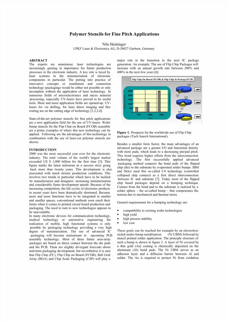
major role in the transition to the next IC packagegeneration. An example: The use of Flip Chip Packages willincrease with an annual growth rate between 200% and400% in the next few years [6].
Figure 1. Prospects for the worldwide use of Flip Chip packages (Tech Search International).
Besides a smaller form factor, the main advantages of anadvanced package are a greater I/O and functional densitywith more pads, which leads to a decreasing pin/pad pitch.This trend requires higher efforts from the interconnectiontechnology. The first successfully applied advanced
packaging method connects the bond pads of the flippedchip (die) to the substrate by evaporated solder bumps. IBMand Delco used this so-called C4 technology (controlledcollapsed chip connect) as a first direct interconnection
between IC and substrate [7]. Today most of the flippedchip based packages depend on a bumping technique.Contact from the bond pad to the substrate is realized by asolder sphere – the so-called bump – that compensates thetension due to mechanical and thermal stress.
General requirements for a bumping technology are:
• compatibility to existing wafer technologies• high yield• high process stability• low cost
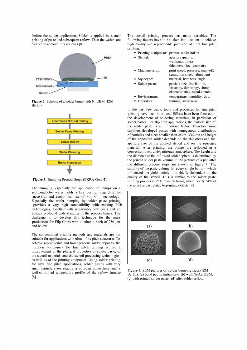
These goals can be reached for example by an electrolessnickel-under-bump metallization (Ni UBM) followed bystencil printed solder application. The principle structure of such a bump is shown in figure 2. A layer of Ni covered bya thin gold (Au) coating is chemically deposited on thealuminum (Al) bond pads. The Ni UBM serves as anadhesion layer and a diffusion barrier between Al andsolder. The Au is required to protect Ni from oxidation
FCIP
27%
FCOB
73%
FCIP
3%
FCOB
97%
FCIP
12%
FCOB
88%
20042004
20002000
19971997
Flip Chip On Board (FCOB) & Flip Chip In Package (FCIP)
0
500
1000
1500
2000
2500
M i l l i o n
o f U n i t s
1997 2000 2004
Year
S o u r c e : T e c h S e a r c h
I n t e r n a t i o n a l
8/6/2019 Polymer Stencils
http://slidepdf.com/reader/full/polymer-stencils 2/7
before the solder application. Solder is applied by stencil printing of paste and subsequent reflow. Then the wafers arecleaned to remove flux residues [8].
Figure 2. Scheme of a solder bump with Ni UBM (IZMBerlin).
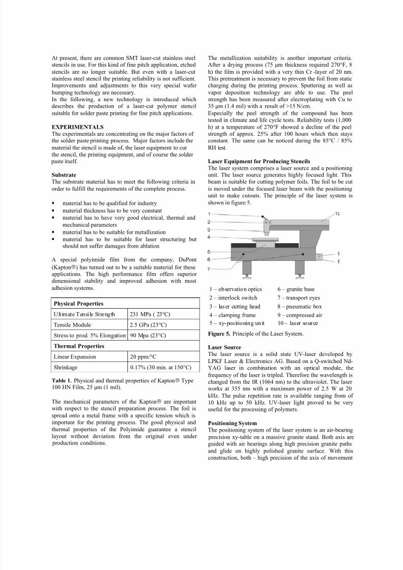
Figure 3. Bumping Process Steps (EKRA GmbH).
The bumping, especially the application of bumps on asemiconductor wafer holds a key position regarding thesuccessful and economical use of Flip Chip technology.Especially the wafer bumping by solder paste printing
provides a very high compatibility with existing PCBtechnologies, together with remarkably low costs and analready profound understanding of the process basics. Thechallenge is to develop this technique for the mass
production for Flip Chips with a suitable pitch of 250 µmand below.
The conventional printing methods and materials are notsuitable for applications with ultra fine pitch structures. Toachieve reproducible and homogeneous solder deposits, the
process techniques for fine pitch printing require animprovement of the physical properties of solder paste, of the stencil materials and the stencil processing technologiesas well as of the printing equipment. Using solder printingfor ultra fine pitch applications, solder pastes with verysmall particle sizes require a nitrogen atmosphere and awell-controlled temperature profile of the reflow furnace[8].
The stencil printing process has many variables. Thefollowing factors have to be taken into account to achievehigh quality and reproducible precision of ultra fine pitch
printing:• Printing equipment: printer, wafer holder • Stencil: aperture quality,
wall smoothness,thickness, size, geometry
• Machine setup: print speed, pressure, snap-off,separation speed, alignment
• Squeegee: material, hardness, angle• Solder paste: particle size, distribution,
viscosity, thixotropy, slumpcharacteristics, metal content
• Environment: temperature, humidity, dust• Operators: training, awareness
In the past few years, tools and processes for fine pitch printing have been improved. Efforts have been focused onthe development of soldering materials, in particular of
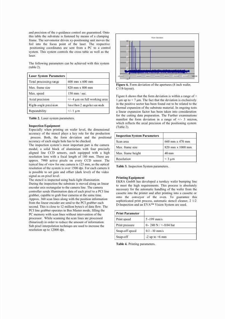
solder pastes. For flip chip applications, the particle size of the solder paste is an important factor. Therefore somesuppliers developed pastes with homogenous distributionsof particles and sizes smaller than 25µm. Volume and heightof the deposited solder depends on the thickness and theaperture size of the applied stencil and on the squeegeematerial. After printing, the bumps are reflowed in aconvection oven under nitrogen atmosphere. The height andthe diameter of the reflowed solder sphere is determined bythe printed solder paste volume. SEM pictures of a pad after the different process steps are shown in figure 4. Thestability of the paste volume for every single bump – whichinfluenced the yield mainly – is chiefly dependent on thequality of the stencil. This is similar to the solder paste
printing process at PCB manufacturing where nearly 64% of the reject rate is related to printing defects [9].
Figure 4. SEM pictures of solder bumping steps (IZMBerlin): (a) bond pad in initial state (b) with Ni/Au UBM,(c) with printed solder paste, (d) after solder reflow.
(b)(a)
(d)(c)
8/6/2019 Polymer Stencils
http://slidepdf.com/reader/full/polymer-stencils 3/7
At present, there are common SMT laser-cut stainless steelstencils in use. For this kind of fine pitch application, etchedstencils are no longer suitable. But even with a laser-cutstainless steel stencil the printing reliability is not sufficient.Improvements and adjustments to this very special wafer
bumping technology are necessary.
In the following, a new technology is introduced whichdescribes the production of a laser-cut polymer stencilsuitable for solder paste printing for fine pitch applications.
EXPERIMENTALS
The experimentals are concentrating on the major factors of the solder paste printing process. Major factors include thematerial the stencil is made of, the laser equipment to cutthe stencil, the printing equipment, and of course the solder
paste itself.
Substrate
The substrate material has to meet the following criteria inorder to fulfill the requirements of the complete process.
• material has to be qualified for industry• material thickness has to be very constant• material has to have very good electrical, thermal and
mechanical parameters• material has to be suitable for metallization• material has to be suitable for laser structuring but
should not suffer damages from ablation
A special polyimide film from the company, DuPont(Kapton) has turned out to be a suitable material for theseapplications. The high performance film offers superior dimensional stability and improved adhesion with mostadhesion systems.
Physical Properties
Ultimate Tensile Strength 231 MPa ( 23°C)
Tensile Module 2.5 GPa (23°C)
Stress to prod. 5% Elongation 90 Mpa (23°C)
Thermal Properties
Linear Expansion 20 ppm/°C
Shrinkage 0.17% (30 min. at 150°C)
Table 1. Physical and thermal properties of Kapton Type100 HN Film, 25 µm (1 mil).
The mechanical parameters of the Kapton are importantwith respect to the stencil preparation process. The foil isspread onto a metal frame with a specific tension which isimportant for the printing process. The good physical andthermal properties of the Polyimide guarantee a stencillayout without deviation from the original even under
production conditions.
The metallization suitability is another important criteria.After a drying process (75 µm thickness required 270°F, 8h) the film is provided with a very thin Cr -layer of 20 nm.This pretreatment is necessary to prevent the foil from staticcharging during the printing process. Sputtering as well asvapor deposition technology are able to use. The peel
strength has been measured after electroplating with Cu to35 µm (1.4 mil) with a result of >15 N/cm.Especially the peel strength of the compound has beentested in climate and life cycle tests. Reliability tests (1,000h) at a temperature of 270°F showed a decline of the peelstrength of approx. 25% after 100 hours which then staysconstant. The same can be noticed during the 85°C / 85%RH test.
Laser Equipment for Producing Stencils
The laser system comprises a laser source and a positioningunit. The laser source generates highly focused light. This
beam is suitable for cutting polymer foils. The foil to be cutis moved under the focused laser beam with the positioningunit to make cutouts. The principle of the laser system isshown in figure 5.
Figure 5. Principle of the Laser System.
Laser Source
The laser source is a solid state UV-laser developed byLPKF Laser & Electronics AG. Based on a Q-switched Nd-YAG laser in combination with an optical module, thefrequency of the laser is tripled. Therefore the wavelength ischanged from the IR (1064 nm) to the ultraviolet. The laser works at 355 nm with a maximum power of 2.5 W at 20kHz. The pulse repetition rate is available ranging from of 10 kHz up to 50 kHz. UV-laser light proved to be veryuseful for the processing of polymers.
Positioning System
The positioning system of the laser system is an air-bearing precision xy-table on a massive granite stand. Both axis areguided with air bearings along high precision granite pathsand glide on highly polished granite surface. With thisconstruction, both – high precision of the axis of movement
1 – observation optics 6 – granite base
2 – interlock switch 7 – transport eyes3 – laser cutting head 8 – pneumatic box
4 – clamping frame 9 – compressed air
5 – xy-positioning unit 10 – laser source
8/6/2019 Polymer Stencils
http://slidepdf.com/reader/full/polymer-stencils 4/7
and precision of the z-guidance control are guaranteed. Ontothis table the substrate is fastened by means of a clampingframe. The servomotor driven xy-positioning unit moves thefoil into the focus point of the laser. The respective
positioning coordinates are sent from a PC to a controlsystem. This system controls the cross table as well as the
laser.
The following parameters can be achieved with this system(table 2).
Laser System Parameters
Total processing range 600 mm x 600 mm
Max. frame size 820 mm x 800 mm
Max. speed 150 mm / sec.
Axial precision +/- 4 µm on full working area
Right-angle precision less than 2 angular seconds
Repeatability +/- 1 µ m
Table 2. Laser system parameters.
Inspection Equipment
Especially when printing on wafer level, the dimensionalaccuracy of the stencil plays a key role for the production
process. Both, the form deviation and the positionalaccuracy of each single hole has to be checked.The inspection system’s most important part is the cameramodul, a solid block of aluminium with four preciselyaligned line CCD sensors, each equipped with a highresolution lens with a focal length of 180 mm. There areapprox. 7900 active pixels on every CCD sensor. Thetypical line of view for one camera is 125 mm, so the optical
resolution of the system is over 1500 dpi. For each camera itis possible to set gain and offset (dark level) of the videosignal as on pixel level.The stencil is inspected using back-light illumination.During the inspection the substrate is moved along an linear encoder axis rectangular to the camera line. The cameracontroller sends illumination data of each pixel to a PCI linegrabber, capable to grab four cameras at the same time.Approx. 360 scan lines along with the position informationfrom the linear encoder are send to the PCI grabber eachsecond. This is close to 12 million bytes/s of data flow. ThePCI line grabber operates in Bus Master mode, filling thePC memory with scan lines without intervention of the
processor. While scanning the scan lines are processed
(binarized) in order to reduce the amount of information.Sub pixel interpolation techniqes are used to increase theresolution up to 12000 dpi.
Figure 6. Form deviation of the apertures (8 inch wafer,C118-layout).
Figure 6 shows that the form deviation is within a range of +1 µm up to + 7 µm. The fact that the deviation is exclusivelyin the positive sector has been found out to be related to thethermal expansion of the substrate material. In ongoing tests
a linear expansion factor has been taken into considerationfor the cutting data preparation. The Further examinationsmanifest the form deviation in a range of +/- 3 micron,which reflects the axial precision of the positioning system(Table 2).
Inspection System Parameters
Scan area 660 mm x 470 mm
Max. frame size 820 mm x 1000 mm
Max. frame height 40 mm
Resolution < 3 µm
Table 3. Inspection System parameters.
Printing Equipment
EKRA GmbH has developed a turnkey wafer bumping lineto meet the high requirements. This process is absolutelynecessary for the automatic handling of the wafer from thecassette into the printer and after printing into a cassette or onto the conveyor of the oven. To guarantee thissophisticated print process, automatic stencil cleaner, 2 1/2D-Inspection and an EVA™ Vision System are used.
Print Parameter
Print speed 5 -199 mm/s
Print pressure 0 - 240 N / +- 0.04 bar
Snap-off speed 0.1 - 10 mm/s
Snap-off -2 up to +6 mm
Table 4. Printing parameters.
Form Deviation
-10
0
10
20
30
40
50
60
-20000 0 20000 40000 60000 80000 100000 120000 140000
8/6/2019 Polymer Stencils
http://slidepdf.com/reader/full/polymer-stencils 5/7
Solder Paste
The solder paste DSC 09-419 from Heraeus was developedfor printing ultra fine pitches. The paste contains anextremely fine powder (Sn63Pb37, type 6). Typical valuesare 10% below 7 µm, 50% below 11 µm and 90% below 16µ m. The values were determined by laser granulometry.
RESULTS AND DISCUSSION
The tests have been performed on 8 inch wafers with benchmark layouts. The final application is an 8 inch wafer with more than 20,000 I/Os. There are two different types of ICs on the wafer. One layout with a 250 µm pitch whichrequires a bump height of 125 µm and one layout with a 200µ m pitch which requires a bump height of 100 µm. Thethickness of the stencil is 75 µm. The apertures in the stencilare 250 µm x 170 µm and 180 µm x 130 µm.
The laser ablation of the polymer material has been opticallyevaluated during the tests. It showed that extensive tests for the determination of an optimum choice of power,frequency and cutting speed are necessary. All three
parameters have an influence on the energy density on thesubstrate. If the power density is too low, the ablation willnot be sufficient to cut through the complete material. Toohigh power densities (>500 mJ/cm²) result in a damage of the substrate material. An optimum combination of
parameters to cut a polyimide film of 75 µm thickness isgiven in table 5.
Laser power 2 W – 3 W
Laser frequency 20 kHz – 30 kHz
Cutting speed 15 mm/s – 25 mm/s
Table 5. Optimum laser cutting parameters, 75 µ m polyimide film.
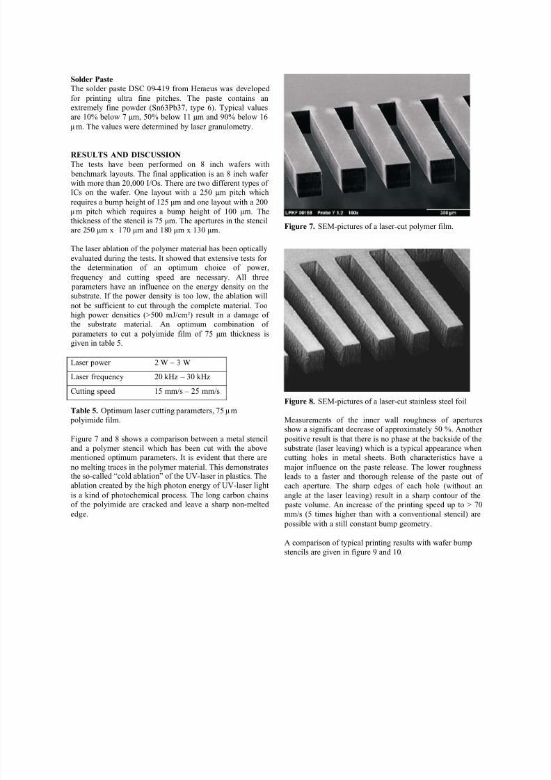
Figure 7 and 8 shows a comparison between a metal stenciland a polymer stencil which has been cut with the abovementioned optimum parameters. It is evident that there areno melting traces in the polymer material. This demonstratesthe so-called “cold ablation” of the UV-laser in plastics. Theablation created by the high photon energy of UV-laser lightis a kind of photochemical process. The long carbon chainsof the polyimide are cracked and leave a sharp non-meltededge.
Figure 7. SEM-pictures of a laser-cut polymer film.
Figure 8. SEM-pictures of a laser-cut stainless steel foil
Measurements of the inner wall roughness of aperturesshow a significant decrease of approximately 50 %. Another
positive result is that there is no phase at the backside of thesubstrate (laser leaving) which is a typical appearance whencutting holes in metal sheets. Both characteristics have amajor influence on the paste release. The lower roughnessleads to a faster and thorough release of the paste out of each aperture. The sharp edges of each hole (without anangle at the laser leaving) result in a sharp contour of the
paste volume. An increase of the printing speed up to > 70mm/s (5 times higher than with a conventional stencil) are
possible with a still constant bump geometry.
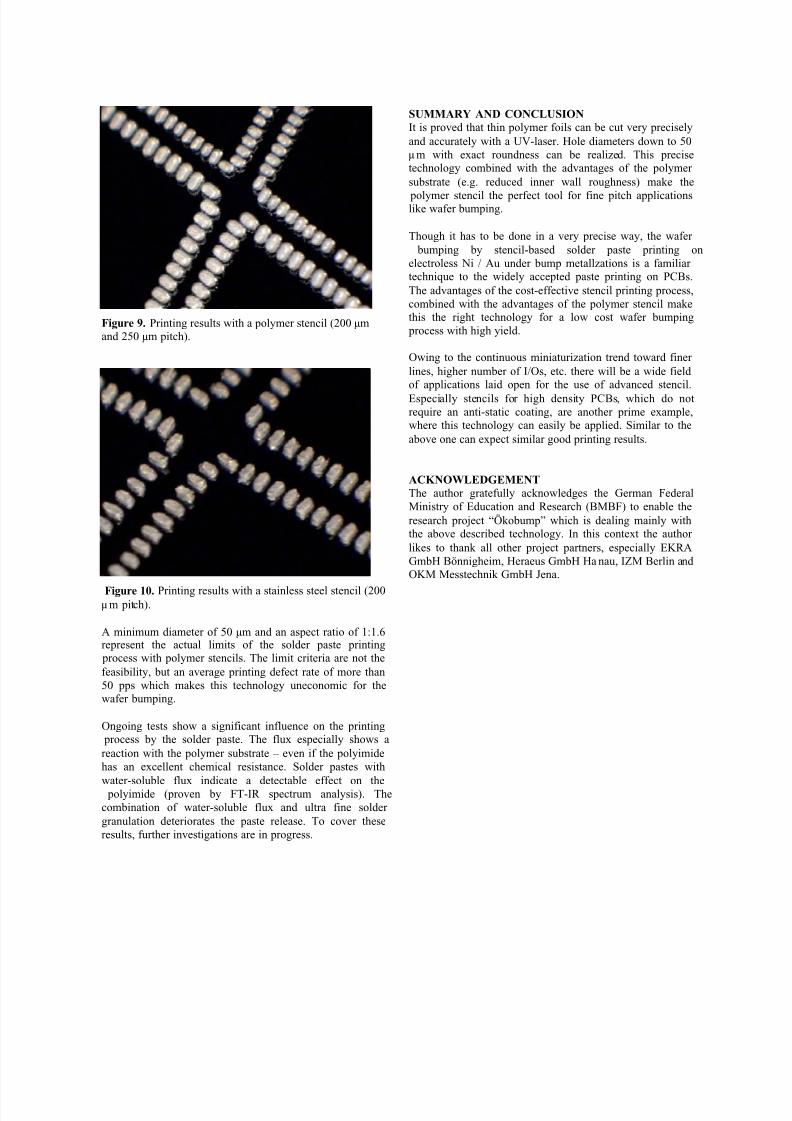
A comparison of typical printing results with wafer bumpstencils are given in figure 9 and 10.
8/6/2019 Polymer Stencils
http://slidepdf.com/reader/full/polymer-stencils 6/7
Figure 9. Printing results with a polymer stencil (200 µmand 250 µm pitch).
Figure 10. Printing results with a stainless steel stencil (200µ m pitch).
A minimum diameter of 50 µm and an aspect ratio of 1:1.6represent the actual limits of the solder paste printing
process with polymer stencils. The limit criteria are not thefeasibility, but an average printing defect rate of more than50 pps which makes this technology uneconomic for thewafer bumping.
Ongoing tests show a significant influence on the printing process by the solder paste. The flux especially shows areaction with the polymer substrate – even if the polyimidehas an excellent chemical resistance. Solder pastes with
water-soluble flux indicate a detectable effect on the polyimide (proven by FT-IR spectrum analysis). Thecombination of water-soluble flux and ultra fine solder granulation deteriorates the paste release. To cover theseresults, further investigations are in progress.
SUMMARY AND CONCLUSION
It is proved that thin polymer foils can be cut very preciselyand accurately with a UV-laser. Hole diameters down to 50µ m with exact roundness can be realized. This precisetechnology combined with the advantages of the polymer substrate (e.g. reduced inner wall roughness) make the
polymer stencil the perfect tool for fine pitch applicationslike wafer bumping.
Though it has to be done in a very precise way, the wafer bumping by stencil-based solder paste printing onelectroless Ni / Au under bump metallzations is a familiar technique to the widely accepted paste printing on PCBs.The advantages of the cost-effective stencil printing process,combined with the advantages of the polymer stencil makethis the right technology for a low cost wafer bumping
process with high yield.
Owing to the continuous miniaturization trend toward finer lines, higher number of I/Os, etc. there will be a wide fieldof applications laid open for the use of advanced stencil.Especially stencils for high density PCBs, which do notrequire an anti-static coating, are another prime example,where this technology can easily be applied. Similar to theabove one can expect similar good printing results.
ACKNOWLEDGEMENT
The author gratefully acknowledges the German FederalMinistry of Education and Research (BMBF) to enable theresearch project “Ökobump” which is dealing mainly withthe above described technology. In this context the author likes to thank all other project partners, especially EKRAGmbH Bönnigheim, Heraeus GmbH Ha nau, IZM Berlin andOKM Messtechnik GmbH Jena.

8/6/2019 Polymer Stencils
http://slidepdf.com/reader/full/polymer-stencils 7/7
REFERENCES
[1] “Mechanical and Laser Via Formation”, by MichaelKauf, Lee Ekblad, Henry Martinez,The Board authority,July 2000, pp. 61
[2] “The wonderful word of LDI and how to realize it”, byMats J. Eklin, The Board Authority, Oktober 2000, p. 51
[3] “Laser Processing of Flex”, by Sri Venkat, PC FABPrinted Circuit Fabrication, February 2001, pp. 28
[4] “Laser Cutting of Flex Circuits”, by Jens Baensch, TheBoard Authority, March 2001, pp. 51
[5] VDMA-Market Information Productronic/ EconomicReport, September 2000
[6] “Advanced IC Packaging Markets and Trends”,Electronic Trend Publications, San Jose, California, 1999
[7] “Flip Chip Packaging for the Year 2000”, by RonaldKuracina, IBM Microelectronics Endicott, New York, 2000
[8] “Quality and Yield of Ultra Fine Pitch Stencil Printing
for Flip Chip Assembly”, by Katrin Heinricht, JoachimKloeser, Liane Lauter, Andreas Ostmann, Andreas Wolter and Herbert Reichl, Eupac 1998, Germany
[9] “Mikroschneiden von SMD-Schablonen für denLotpastendruck”, by Jörg Kickelhain, LEF 2000, Germany