Piezoelectric Spectroscopy of the Defects States on the Surfaces of Semiconducting Samples M....
21
Piezoelectric Spectroscopy of the Defects States on the Surfaces of Semiconducting Samples M. Maliński 1 , J. Zakrzewski 2 , K. Strzałkowski 2 , F. Firszt 2 1 Department of Electronics and Computer Science, Technical University of Koszalin, 2 Śniadeckich St, 75–328 Koszalin, Poland 2 Instytut Fizyki, Uniwersytet Mikołaja Kopernika, ul.Grudziadzka 5/7, 87–100 Torun,
-
Upload
harvey-nicholas-stewart -
Category
Documents
-
view
214 -
download
0
Transcript of Piezoelectric Spectroscopy of the Defects States on the Surfaces of Semiconducting Samples M....

Piezoelectric Spectroscopy of the Defects States on the Surfaces of
Semiconducting Samples
M. Maliński1, J. Zakrzewski2, K. Strzałkowski2, F. Firszt2
1 Department of Electronics and Computer Science, Technical
University of Koszalin,
2 Śniadeckich St, 75–328 Koszalin, Poland
2 Instytut Fizyki, Uniwersytet Mikołaja Kopernika, ul.Grudziadzka 5/7,
87–100 Torun, Poland

ABSTRACT
This presentation shows both theoretical and experimental aspects connected with piezoelectric detection of defects’ states located on surfaces of semiconducting samples. This kind of states can provide absorption bands visible in the energy gap region of semiconductors. Theoretical considerations presented in this paper comprise computations of the piezoelectric spectra for defects’ states located on different surfaces. Experimental part of the paper comprises numerical analysis of several experimental amplitude and phase piezoelectric spectra of a group of Zn1-x-yBeyMnxSe mixed crystals for different x, y compositional parameters i.e. y=0.05, x=0.05, 0.10, 0.15, 0.20 after different surface treatment.

SAMPLE PREPARATION & THE MEASURING METHOD
Zn1-x-yBexMnySe (x=0.05, y= 0.05, 0.10, 0.15 and 0.20) samples were grown
from the high purity powder with the high pressure Bridgman method. The crystal rod was cut into about 1mm thick samples which were first grinded, then polished with diamond paste and finally chemically etched. Solution of H2SO4 (96%), K2Cr2O7 and water was used for etching the samples. After
etching, the samples were rinsed in distilled water and then put for a few seconds in boiling NaOH. Then the samples were rinsed again in cold and next in boiling distilled water and finally in ethyl alcohol.
In the piezoelectric photothermal experiment samples were illuminated with the intensity modulated beam of light of a xenon lamp after passing through the prism monochromator. The piezoelectric signal was detected with a lock-in phase selective amplifier. The characteristics were measured at room temperature in the rear experimental configurations.

INTRODUCTION
Typical optical transmission measurements do not bring information on the spatial locations of the defects responsible for the absorption bands. Another basic problem of this type of measurements is the lack of the possibility of identification of the type of the optical absorption i.e. a bulk or surface one.
Piezoelectric phase measurements bring information on the spatial location of the absorbing centers!
Numerical analysis of the PZE spectra can also bring information on the type of absorption: a volume or a surface one.
THEORY
Let’s consider the surface type optical absorption coefficient spectra connected with the presence of surface defects in the form of the Gaussian distribution
2
2/1
2/1exp2/1)(2/1
EEAE
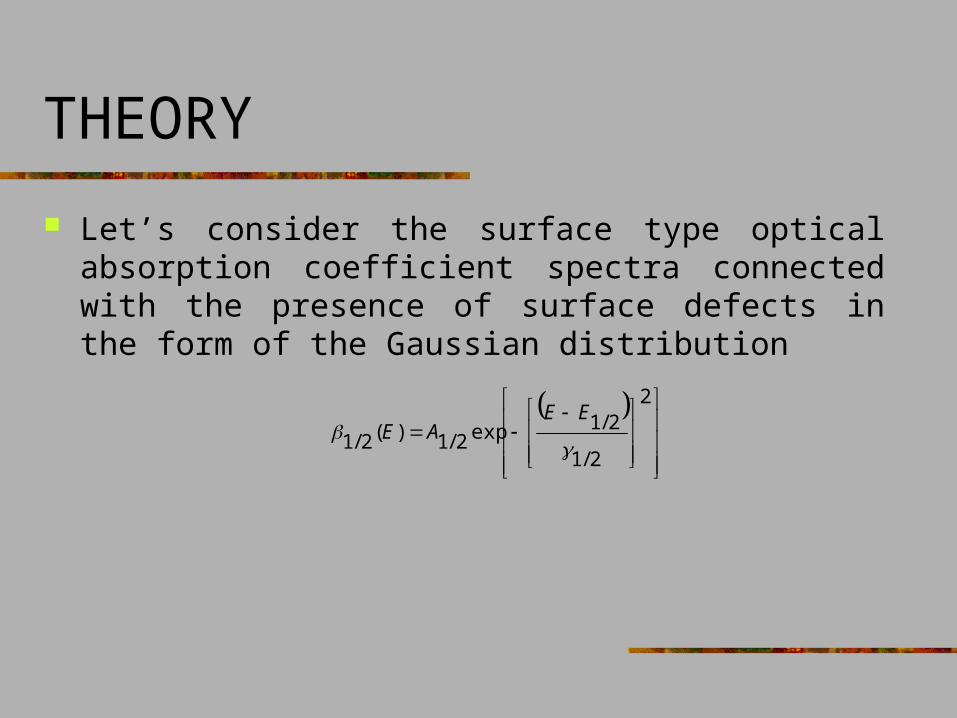
THEORY
The bulk type optical absorption coefficient spectra in the Urbach edge energy region, below the energy gap value, and in the band to band absorption region, above the energy gap value, are given by the formulae:
025.03exp3)(3
gEEAE
)(34)(4 EggEEAE

PIEZOELECTRIC SIGNAL
Piezoelectric signal S is computed according to Jackson& Amer formula.
T(x) is the temperature distribution in the sample
l ldxxTx
l
ldxxT
lS
0 0)(
226
)(1
),(),(),()( 32211 xTxTxTxT

DIAGRAM OF A SAMPLE
0 l
I 0
S 1 S 2
d d
I 0
T 1 (x,)
))))
T 2 (x,)
)

TEMPERATURE DISTRIBUTIONSSURFACE & VOLUME ABSORPTION
)2exp(1
)2exp()exp()1exp(10),(1 l
xlxdsIxT
)2exp(1
)(2exp())(exp()2exp(10),(2 l
xllxldsIxT
l
xNxMIxT
2exp12
,,0),(
lxlxllxlxlxxxM
exp2expexp2expexpexp,
llxxlxxlxlxxN
expexpexp2exp2expexp,

THEORY-surface absorption
Parameters of the surface absorption band: Eg=2.81 eV,
A3=80 cm-1,=1, E1=2.18 eV, 1=0.13 eV, A1=290 cm-1.
1.5 2 2.5 30
500
1000
ENERGY [eV]
OP
TIC
AL
AB
S.
CO
EF
F
[cm
-1]

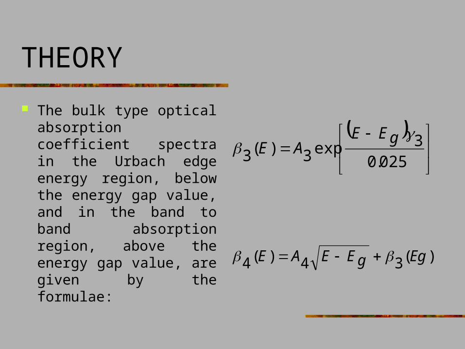
THEORY- PZE SPECTRA
Piezoelectric amplitude and phase spectra computed for the parameters: =0.03 cm2/s, f=36 Hz and l=0.1 cm & the rear experimental configuration.
The defect located on the illuminated side of the sample
2 2.5 30
5 104
0.001
0.0015
0.002
0.0025
ENERGY [eV]
AM
PL
ITU
DE
[a.
u]
2 2.5 3100
50
0
50
100
ENERGY [eV]
PH
AS
E [
degs
]

THEORY- PZE SPECTRA
The defect located on the dark side of the sample. Parameters: =0.03 cm2/s, f=36 Hz and l=0.1 cm
2 2.5 30
5 104
0.001
0.0015
0.002
0.0025
ENERGY [eV]
AM
PL
ITU
DE
[a.
u]
2 2.5 3100
50
0
50
100
ENERGY [eV]
PH
AS
E [
degs
]
THEORY- PZE SPECTRA
The defect located on the illuminated and dark side of the sample.
Parameters: =0.03 cm2/s, f=36 Hz and l=0.1 cm
2 2.5 30
5 104
0.001
0.0015
0.002
0.0025
ENERGY [eV]
AM
PL
ITU
DE
[a.
u]
2 2.5 3100
50
0
50
100
ENERGY [eV]
PH
AS
E [
degs
]

THEORY- PZE SPECTRA
Piezoelectric spectra - under the assumption of the volume absorption type connected with the defect center at E=2.18 eV .
Parameters: =0.03 cm2/s, f=36 Hz and l=0.1 cm
2 2.5 30
5 104
0.001
0.0015
0.002
0.0025
ENERGY [eV]
AM
PL
ITU
DE
[a.
u]
2 2.5 3100
50
0
50
100
ENERGY [eV]
PH
AS
E [
degs
]

EXPERIMENTAL RESULTS
Piezoelectric amplitude a) and phase b) spectra of the Zn0.75Be0.05Mn0.20Se sample at f=126 Hz in the rear configuration.
Circles are experimental points, solid lines are theoretical curves.
.
2 2.5 30
0.5
1
1.5
ENERGY [eV]
AM
PL
ITU
DE
[a.
u]
2 2.5 3100
50
0
50
100
150
ENERGY [eV]
PH
AS
E [
deg]

EXPERIMENTAL RESULTS
Optical parameters of the center determined: A1=290 cm-1, 1=0.13 eV, E1=2.18 eV, Eg=2.81 eV, 3=1. The center is located on the illuminated side of the sample.
1.5 2 2.5 30
500
1000
ENERGY [eV]
OP
TIC
AL
AB
S.
CO
EF
F
[cm
-1]
EXPERIMENTAL RESULTS
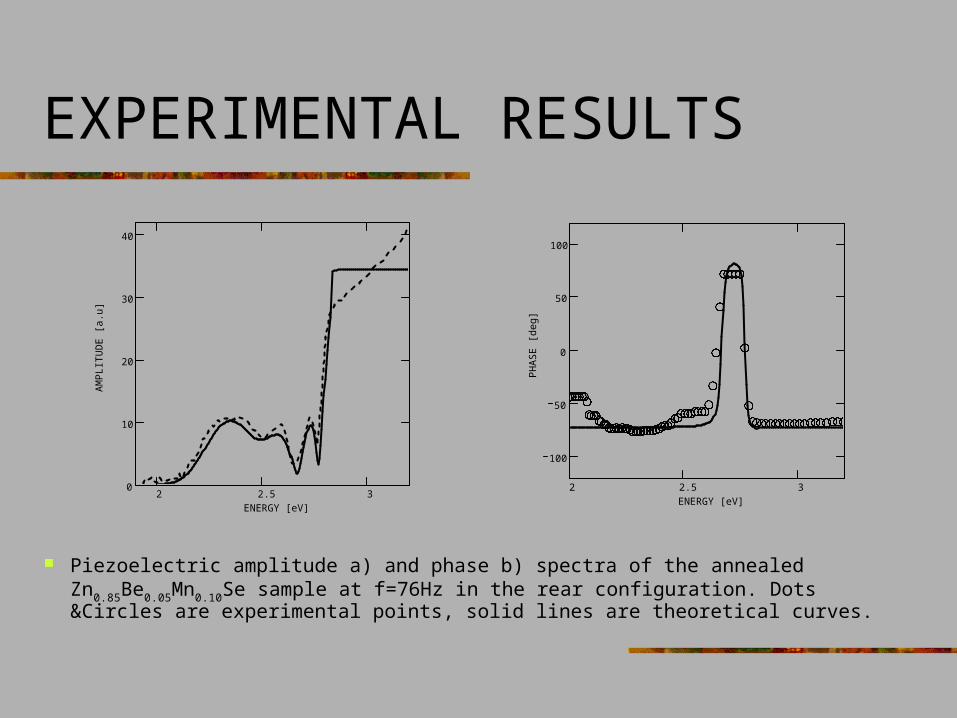
Piezoelectric amplitude a) and phase b) spectra of the annealed Zn0.85Be0.05Mn0.10Se sample at f=76Hz in the rear configuration. Dots &Circles are experimental points, solid lines are theoretical curves.
.
2 2.5 30
10
20
30
40
ENERGY [eV]
AM
PL
ITU
DE
[a.
u]
2 2.5 3
100
50
0
50
100
ENERGY [eV]
PH
AS
E [
deg]

OPTICAL ABS. COEFF. SPECTRUM
Parameters of these surface absorption bands determined: A1 = 350 cm-1, A2 = 260 cm-1, E1 = 2.35 eV, E2 = 2.60 eV, 1 = 0.15 eV, 2 =
0.15 eV. Both defects are located on the same, illuminated, side of the sample.
2 2.2 2.4 2.6 2.8 3 3.20
200
400
600
800
1000
ENERGY [eV]
OP
TIC
AL
AB
S.
CO
EF
F
[cm
-1]

EXPERIMENTAL RESULTS
Experimental and theoretical PZE amplitude a) and phase b) spectra of Zn0.75Be0.05Mn0.20Se sample measured at f=76 Hz
Circles-exp. results, lines- theoretical curves
2 2.5 3 0
10
20
30
ENERGY [eV]
AM
PLIT
UD
E [
a.u]
2 2.5 3200
100
0
100
200
300
ENERGY [eV]P
HA
SE
[de
g]

CONCLUSIONS
Theoretical considerations, presented in the paper, indicate that it is possible to determine the location of the surface defects, visible in the amplitude piezoelectric spectra, on one of the surfaces of the sample from the numerical analysis of the piezoelectric phase spectra.
Theoretical and experimental results analysed in the paper also proved the possibility of distinguishing between the bulk and surface absorption.

THANK YOU FOR YOUR ATTENTION