PhysRevstab 17.013501 - Physical Review Journals
11
Investigating crystal microstructure of niobium materials by an x-ray diffraction reciprocal space mapping technique Qiguang Yang, 1 Frances Williams, 1 Xin Zhao, 2,* Charles Reece, 2 and Mahadevan Krishnan 3 1 Center for Materials Research, Norfolk State University, Norfolk, Virginia 23504, USA 2 Thomas Jefferson National Accelerator Facility, Newport News, Virginia 23606, USA 3 Alameda Applied Sciences Corporation (AASC), San Leandro, California 94577, USA (Received 20 August 2013; published 10 January 2014) An x-ray diffraction reciprocal spacing mapping (RSM) technique was applied to investigate crystal quality of Nb films and bulk materials, relevant to superconducting radio frequency applications. The RSM study used different x-ray penetration depths to study material processes after two different surface treatments: mechanical polishing or energetic condensation (a plasma process). The study revealed the material’ s microstructure evolution for the two different processes. The RSM plots revealed crystal quality of the materials at different thickness. The novel, differential-depth RSM technique presented in this study substantiated the following facts: (1) For a heteroepitaxial Nb film Nbð100Þ=MgOð100Þ, a film thickening process, via a cathodic arc-discharge Nb ion deposition (energetic condensation), created a near-perfect single crystal Nb on the surface top layer. (2) For a fine mechanically polished single-crystal bulk Nb material, the microstructure on the top surface layer is more disordered than that at a greater depth. DOI: 10.1103/PhysRevSTAB.17.013501 PACS numbers: 81.15.Fg, 68.55.J- I. INTRODUCTION Superconducting radio frequency (SRF) accelerating cavities for particle accelerators that are made of a bulk niobium (Nb) material or with a Nb thin film coated on Cu or other substrates, are used in state-of-the-art facilities for exploring frontier physics, such as the Continuous Electron-Beam Accelerator Facility at the Thomas Jefferson National Accelerator Facility (Jefferson Lab), the European X-ray Free Electron Laser, the Facility for Rare Isotope Beams, the Spallation Neutron Source, and the proposed International Linear Collider. Nb film coated copper cavities had earlier successfully served the Large Electron Positron Collider project at CERN in the 1990s. Next-generation SRF particle accelerators call for revolutionary new materials or new surface treatment proc- esses, in order to be more energy efficient and be more materials-cost frugal. To design and develop an optimal SRF material process, it is necessary to adopt new analytic techniques to nondes- tructively characterize the SRF functional layer less than 200 nm into the surface. One is interested in understanding the crystal quality of the superconductor within this depth. The definition and measurement of crystal quality in this text is based on crystallographic long-range order (coher- ence) of atoms, but not on chemical impurities. As was pointed out by Cullity et al. [1,2], the quality of so-called “single crystals” or grains, varies from one case to another. At one extreme, a grain might have gone through plastic deformation, such that some portions (subgrains) of the grain are misoriented from the others, thus the dislocation density is high; at the other extreme, some precisely grown crystals have ultralow density of dislocations, line or planar imperfections (stacking faults), and their crystal planes in that single grain are flat to less than 10 -4 ° over a distance of centimeters. Essentially, a motivation of this study is to quantify the density of intragrain defects in Nb materials by diffraction techniques. In recent years, our research found that energetic conden- sation is a practical way to create high quality Nb film materials [3–7]. Energetic condensation has been accom- plished by a cathodic-arc-discharge [7] or an electron cyclotron resonant Nb plasma ion source [8]. To understand the structural evolution of SRF Nb films grown via ener- getic condensation is an important and challenging task. To characterize SRF materials, one convenient choice in the SRF community is the electron backscattering diffrac- tion (EBSD) technique. EBSD has been widely used [9] to investigate the microstructure of Nb materials (thin film or bulk). The probing depth of EBSD is ∼50 nm, which is comparable to the SRF London penetration depth. Therefore, EBSD measurements have provided useful insights into SRF materials in many studies [10,11]. A popular choice of the EBSD tool, is commercial soft- ware of the EDAX/TSL company. The program is called OIM Data Collections and Analysis. The OIM stands for crystallographic “orientation indexing mapping” of crys- tals, which is the core value of a commercially available EBSD toolbox. It is to be noted that a plurality of grains are surveyed in a conventional EBSD study. * [email protected] Published by the American Physical Society under the terms of the Creative Commons Attribution 3.0 License. Further distribu- tion of this work must maintain attribution to the author(s) and the published articles title, journal citation, and DOI. PHYSICAL REVIEW SPECIAL TOPICS - ACCELERATORS AND BEAMS 17, 013501 (2014) 1098-4402=14=17(1)=013501(11) 013501-1 Published by the American Physical Society
Transcript of PhysRevstab 17.013501 - Physical Review Journals

Investigating crystal microstructure of niobium materials by an x-raydiffraction reciprocal space mapping technique
Qiguang Yang1 Frances Williams1 Xin Zhao2 Charles Reece2 and Mahadevan Krishnan31Center for Materials Research Norfolk State University Norfolk Virginia 23504 USA2Thomas Jefferson National Accelerator Facility Newport News Virginia 23606 USA3Alameda Applied Sciences Corporation (AASC) San Leandro California 94577 USA
(Received 20 August 2013 published 10 January 2014)
An x-ray diffraction reciprocal spacing mapping (RSM) technique was applied to investigate crystalquality of Nb films and bulk materials relevant to superconducting radio frequency applications TheRSM study used different x-ray penetration depths to study material processes after two different surfacetreatments mechanical polishing or energetic condensation (a plasma process) The study revealed thematerialrsquos microstructure evolution for the two different processes The RSM plots revealed crystal qualityof the materials at different thickness The novel differential-depth RSM technique presented in this studysubstantiated the following facts (1) For a heteroepitaxial Nb film Nbeth100THORN=MgOeth100THORN a film thickeningprocess via a cathodic arc-discharge Nb ion deposition (energetic condensation) created a near-perfectsingle crystal Nb on the surface top layer (2) For a fine mechanically polished single-crystal bulk Nbmaterial the microstructure on the top surface layer is more disordered than that at a greater depth
DOI 101103PhysRevSTAB17013501 PACS numbers 8115Fg 6855J-
I INTRODUCTION
Superconducting radio frequency (SRF) acceleratingcavities for particle accelerators that are made of a bulkniobium (Nb) material or with a Nb thin film coated onCu or other substrates are used in state-of-the-art facilitiesfor exploring frontier physics such as the ContinuousElectron-Beam Accelerator Facility at the ThomasJefferson National Accelerator Facility (Jefferson Lab)the European X-ray Free Electron Laser the Facility forRare Isotope Beams the Spallation Neutron Source andthe proposed International Linear Collider Nb film coatedcopper cavities had earlier successfully served the LargeElectron Positron Collider project at CERN in the 1990sNext-generation SRF particle accelerators call for
revolutionary new materials or new surface treatment proc-esses in order to be more energy efficient and be morematerials-cost frugalTo design and develop an optimal SRF material process
it is necessary to adopt new analytic techniques to nondes-tructively characterize the SRF functional layer less than200 nm into the surface One is interested in understandingthe crystal quality of the superconductor within this depthThe definition and measurement of crystal quality in this
text is based on crystallographic long-range order (coher-ence) of atoms but not on chemical impurities As waspointed out by Cullity et al [12] the quality of so-called
ldquosingle crystalsrdquo or grains varies from one case to anotherAt one extreme a grain might have gone through plasticdeformation such that some portions (subgrains) of thegrain are misoriented from the others thus the dislocationdensity is high at the other extreme some precisely growncrystals have ultralow density of dislocations line or planarimperfections (stacking faults) and their crystal planes inthat single grain are flat to less than 10minus4deg over a distance ofcentimeters Essentially a motivation of this study is toquantify the density of intragrain defects in Nb materialsby diffraction techniquesIn recent years our research found that energetic conden-
sation is a practical way to create high quality Nb filmmaterials [3ndash7] Energetic condensation has been accom-plished by a cathodic-arc-discharge [7] or an electroncyclotron resonant Nb plasma ion source [8] To understandthe structural evolution of SRF Nb films grown via ener-getic condensation is an important and challenging taskTo characterize SRF materials one convenient choice in
the SRF community is the electron backscattering diffrac-tion (EBSD) technique EBSD has been widely used [9] toinvestigate the microstructure of Nb materials (thin film orbulk) The probing depth of EBSD is sim50 nm which iscomparable to the SRF London penetration depthTherefore EBSD measurements have provided usefulinsights into SRF materials in many studies [1011]A popular choice of the EBSD tool is commercial soft-
ware of the EDAXTSL company The program is calledOIM Data Collections and Analysis The OIM stands forcrystallographic ldquoorientation indexing mappingrdquo of crys-tals which is the core value of a commercially availableEBSD toolbox It is to be noted that a plurality of grainsare surveyed in a conventional EBSD study
xinzhaojlaborg
Published by the American Physical Society under the terms ofthe Creative Commons Attribution 30 License Further distribu-tion of this work must maintain attribution to the author(s) andthe published articles title journal citation and DOI
PHYSICAL REVIEW SPECIAL TOPICS - ACCELERATORS AND BEAMS 17 013501 (2014)
1098-4402=14=17(1)=013501(11) 013501-1 Published by the American Physical Society
The limit of the EBSD technique is that the state-of-artEBSD instrument is mainly applied to visualize orientationof multiple crystals or grains (intergrainsrsquo characteristicsgrain boundaries angles grain size etc) A single crystalrsquosquality or intragrainrsquos density of structural defects isbeyond the primary scope of the OIM technique Only afew indirect parameters in the EBSD OIM software suchas crystal-orientation indexing confidence index (CI) orKikuchi pattern imaging quality (IQ) extracted from theEBSD imaging data set might shed qualitative light onintragrain crystal quality To relate our measurements toconventional EBSD mapping techniques we have pre-sented the measured CI and IQ values as benchmarksThus the EBSD technique has its limitation as a tool forcharacterizing the individual grains or crystalsResearch on crystal quality is sensitive to subtle
deviation of crystal planes (eg bending twisting polygo-nization) or plane distance (dhkl which is proportional tothe lattice constant) Outside the SRF community inscientific research of semiconductors [12ndash16] macromo-lecular crystal proteins [2] and optic electronics [17]the x-ray diffraction reciprocal space mapping technique(XRD RSM) has been widely utilized for example to mea-sure the structural properties of epitaxial films or to revealfilm composition layer tilting lattice relaxation and crys-tal quality Such RSM plots could demonstrate the strainrelaxation and misorientation of a thin film on a substrateThe detection area of an x-ray machine could be a fewsquare centimeters In a RSM plot both Δθhkl (latticeconstant deviation) and Δω (crystal planes misorientation)are observable Different structural properties may berevealed in one graphHere we describe a novel RSM technique using x-ray
penetration of a sample (film or bulk) to different depthsThe depth variation is accomplished by varying the incidentangle of the x-rays Thus this new technique allows non-destructive investigation of a materialrsquos structural characterat different depths It can reveal structural evolution of aSRF material after different processes such as film coatingpolishing or heating
II EXPERIMENTAL METHOD
To validate the use of RSM for Nb materials study threetypes of representative coupon samples were selected Theywent through different materials processes It is expectedthat these representatives have distinct microstructurecharacter in surface and in the bulk layer For this studythe surface thickness of interest is less than 100 nmbecause only this depth is relevant to the RF London pen-etration depth in a SRF applicationFilm samples dubbed CED-34 CED-38 and CED-47
are Nb films that were coated on single crystalMgO (100) substrates using energetic condensation [5]The bulk sample Nb-SC-01 is a single crystal Nb couponSample Nb-PC-01 is a polycrystalline bulk Nb coupon
The deposition method of making film samples has beendescribed elsewhere [518] The energetic condensationwas conducted via a cathodic arc-discharge Nb ion depo-sition Such a Nb plasma ion uses a low voltage (30 V) arcdischarge to generate highly ionized plasma The energyspectrum of ions from coaxial energetic deposition(CED) ranges from 20 eV up to 170 eV The CED facilitywas run in a pulse mode and the pulse lasts 1 ms duringwhich sim05 nm of Nb is deposited on the substrateThe instantaneous deposition rate is as high as560 nm=s The estimated (instantaneous) ion flux is1018Nb ions=cm2 minus sThe repetition rate (frequency) ofthe arc or pulse is 05 Hz limited by silicon controlled rec-tifier switches but may be increased by using insulated gatebipolar transistor switches to more rapidly turn off the arcbetween pulses By considering the dead time and fre-quency of the arcs the nominal deposition rate issim3 Aring=s or roughly one atomic monolayer per secondThis nominal deposition rate is similar to a conventionalphysical vapor deposition method such as a magnetronsputtering source (167 nm=s) or the electron cyclotron res-onant Nb plasma source at Jefferson Lab (225 nm=s)The bulk Nb coupons Nb-SC-01 and Nb-PC-01
(10 times 10 times 3 mm) were chemically mechanically polished(CMPrsquoed process) at the WahChang company The CMP isa ldquomirror-finishingrdquo process to obtain an ultraflat surfaceAfter CMP the samples were lightly chemically etched fora few μm to remove the ldquodamage layerrdquo that is caused bythe mechanical polish The etch used was the typicalldquobuffered chemical polishrdquo (BCP) applied to niobiumAfter the BCP process most of the impurity residuals orcrystallographic defects were removed The surfaceappeared very shiny and morphologically flat under thescanning electron microscope The samplesrsquo surface rough-ness (RRMS) measured by atomic force microscopy aresim40 nm on a 50 times 50 μm survey areaThe residual resistance radio (RRR) values of the Nb
film samples were measured at the vertical cryogenic test-ing area of Jefferson Lab The testing methods have beenreported elsewhere [518] As a measurement of direct cur-rent electrical properties this value embodies the density ofstructural defects of a conductive sample (usually a metal)In this study the RRR value is defined as the ratio of resis-tivity at 300 K to that at 10 K Noticeably because ourmeasurement obtains a RRR value across the entire filmthickness about a fewμm this bulk property (RRR) is dif-ferent [5] from a local zone RRR (such as the surfacelayerrsquos RRR) In this research only the RRR of film sam-ples (not bulk ones) were tested and reportedPole figure and reciprocal space mapping measurements
were performed at Norfolk State University using a highresolution four-circle PANalytical XrsquoPert Pro Materialsresearch diffracto meter The system was especiallydesigned for thin film analysis and operated with a CuKα x-ray source at a wavelength of 154 AringUnless specified
YANG et al Phys Rev ST Accel Beams 17 013501 (2014)
013501-2
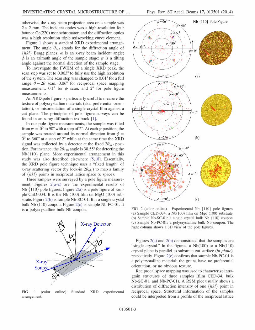
otherwise the x-ray beam projection area on a sample was2 times 2 mm The incident optics was a high-resolution fourbounce Ge(220) monochromator and the diffraction opticswas a high resolution triple axisrocking curve elementFigure 1 shows a standard XRD experimental arrange-
ment The angle θhkl stands for the diffraction angle offhklg Bragg planes ω is an x-ray beam incident angleϕ is an azimuth angle of the sample stage ψ is a tiltingangle against the normal direction of the sample stageTo investigate the FWHM of a single XRD peak the
scan step was set to 0003deg to fully use the high resolutionof the system The scan step was changed to 001deg for a fullrange θ minus 2θ scan 006deg for reciprocal space mappingmeasurement 01deg for ϕ scan and 2deg for pole figuremeasurementsAn XRD pole figure is particularly useful to measure the
texture of polycrystalline materials (aka preferential orien-tation) or misorientation of a single crystal film against acut plane The principles of pole figure surveys can befound in an x-ray diffraction textbook [1]In our pole figure measurements the sample was tilted
from ψ frac14 00 to 90deg with a step of 2deg At each ψ position thesample was rotated around its normal direction from ϕ frac1400 to 360deg at a step of 2deg while at the same time the XRDsignal was collected by a detector at the fixed 2θhkl posi-tion For instance the 2θ110 angle is 3855deg for detecting theNbf110g plane More experimental arrangement in thisstudy was also described elsewhere [518] Essentiallythe XRD pole figure technique uses a ldquofixed lengthrdquo ofx-ray scattering vector (by lock-in 2θhkl) to map a familyof fhklg points in reciprocal lattice space (k space)Three samples were surveyed by a pole figure measure-
ment Figures 2(andashc) are the experimental results ofNb f110g pole figures Figure 2(a) is a pole figure of sam-ple CED-034 It is the Nb (100) film on MgO (100) sub-strate Figure 2(b) is sample Nb-SC-01 It is a single crystalbulk Nb (110) coupon Figure 2(c) is sample Nb-PC-01 Itis a polycrystalline bulk Nb coupon
Figures 2(a) and 2(b) demonstrated that the samples areldquosingle crystalrdquo In the figures a Nb(100) or a Nb(110)crystal plane is parallel to substrate cut surface (in plane)respectively Figure 2(c) confirms that sample Nb-PC-01 isa polycrystalline material the grains have no preferentialorientation or no obvious textureReciprocal space mapping was used to characterize intra-
grain structures of three samples (film CED-34 bulkNb-SC-01 and Nb-PC-01) A RSM plot usually shows adistribution of diffraction intensity of one fhklg point inreciprocal space Structural information of the samplescould be interpreted from a profile of the reciprocal lattice
FIG 1 (color online) Standard XRD experimentalarrangement
FIG 2 (color online) Experimental Nb f110g pole figures(a) Sample CED-034 a Nb(100) film on Mgo (100) substrate(b) Sample Nb-SC-01 a single crystal bulk Nb (110) coupon(c) Sample Nb-PC-01 a polycrystalline bulk Nb coupon Theright column shows a 3D view of the pole figures
INVESTIGATING CRYSTAL MICROSTRUCTURE OF hellip Phys Rev ST Accel Beams 17 013501 (2014)
013501-3
point Experimental RSM data is presented in a two-dimensional ldquoω vsω=2θrdquo plot The ω=2θ means themachine running under a coupled ω=2θ scan mode alsoknown as a θ=2θ (Bragg-Brentano) scan mode Its xcoordinate represents variable θBy Braggrsquos law 2dhkltimes sin ethθhklTHORN frac14 λCuKα Δθhkl is pro-
portional to the distortion of lattice space (Δdhkl) A broad-ening effect along the θhkl coordinate indicates variation indhkl (spacing of crystal planes fhklg) dhkl is proportionalto the lattice constant (a) of Nb which is a body-centeredcubic structure and
dhkl frac14 a=ffiffiffiffiffiffiffiffiffiffiffiffiffiffiffiffiffiffiffiffiffiffiffiffi
h2 thorn k2 thorn l2p
thus the Nb lattice distortion Δa=aethTHORN can be derivedfrom ΔθhklA broadening in the ω direction (or Δω) embodies a
misorientation spread of a fhklg crystal plane whichimplies structural imperfection in the sample (grain) dueto ldquomosaic spreadrdquo (evidence of subgrains) dislocationspopulation bending or polygonization of a latticeBefore each RSM survey an fhklg Bragg plane (or θhkl)
an x-ray incident angle (ω0) an azimuth angle (ϕ) and asample stage tilting angle (ψ) were selected in order toprobe a specific penetration depth in a particular sampleThen the XRD machine scans in a ω=2θ mode at differentω offset Scan step of ω or 2θ is 006degTo calculate penetration depth (t) of an x-ray beam this
equation from Cullityrsquos book [1] is applied
t frac14 sin α=μ
Here α is an incident angle μ frac14 1259 it is the absorptioncoefficient of Nb at λCuKα frac14 154 AringBy controlling the penetration depth we could either
investigate the RSM of a surface layer which is a few hun-dred nanometers or probe that of a thicker (includes inte-gration over the surface) layer By comparison of RSMplots of a thinner layer to that of a thicker layer onemay discriminate the microstructure at different depthsThis may reveal the structure evolution of the Nb sampleafter a coating or polishingFor a shallow and a thick penetration survey although
different reciprocal points in k space were observed viaRSM it is still reasonable and meaningful to compare pro-files of the points This is because (1) in the same samplemeasurement the observed reciprocal points belong to the
same fhklg crystal plane family and (2) A Nb crystal lat-tice is a cubic structure whose symmetry determines that adeviation of one fhklg shall lead to a proportional deviationof the other fhklg points since the volume of a cubic ldquoboxrdquolattice shall be conservativeIt is also worth noting that such a comparison is only
qualitative in order to give a hint of crystallographic dis-order Because a strain of the lattice is always three dimen-sional while the state-of-art RSM is a two-dimensional plotof such incoherence lattices it is unrealistic to apply a 2Dgraph to depict a 3D lattice This is not a problem particularto our RSM study but a conventional challenge to visualize3D space structure by XRDThe EBSD system being utilized in this study being
made by the EDAXTSL company is installed on anAmray scanning electron microscope at Jefferson LabThe EBSD arrangement is equipped with EDAXTSL com-panyrsquos OIMtrade software to acquire and index the crystallo-graphic orientationsIn this study two parameters related to crystal quality
were recorded for parallel comparison The abbreviationof ldquoAvg CIrdquo means the average confidence index whileldquoAvg IQrdquo means the average image quality of theKikuchi imaging pattern (an electron backscattering dif-fraction pattern) Higher CI means the TSL crystal orien-tation indexing software has a higher confidence to indexthe crystal zone and orientation under that e-beam scanspot Higher IQ means the Kikuchi imaging pattern (beingoriginated at a single e-beam scan spot) is sharper For astrained zone then a spot with a high density of crystallo-graphic defects has a Kikuchi image quality worse than thatof a perfect crystal zone
III RESULTS AND DISCUSSION
A Crystal quality evolution via film thickening
1 Investigation of a Nb epitaxy film at differentpenetration depths by RSM
In our previous studies [518] a trend became obviousthat by coating a thicker Nb film average crystal qualityof a single crystal Nb film is advanced as representedby the RRR value a bulk electrical propertyIt was suspected that the crystal quality of a filmrsquos top
layer has been progressively improved as the grains werebeing continuously thickened (in other words the graingrows up) To confirm our speculation we selected two
TABLE I Two RSM experimental arrangements to measure f123g reciprocal points at different x-ray penetration depths Samplelabel is CED-34 It is a Nb film on MgO (100) substrate
Arrangement Omega ωethdegTHORN 2Theta 2θethdegTHORN Psi ψethdegTHORN PhiϕethdegTHORNX-ray penetration
depthSpread of ω atFWHMΔωethdegTHORN
Spread of θ atFWHMΔθethdegTHORN
11 31 12182 061 2845 Shallow sim430 nm 01 0112 273 12187 5832 2765 Thick sim365 um 06 02
YANG et al Phys Rev ST Accel Beams 17 013501 (2014)
013501-4
material analysis techniques (RSM and EBSD) to probe thecrystal quality of sample Nb filmsInitially Nb film sample CED-34 was surveyed by RSM
This film sample was coated by a typical Alameda Applied
Sciences Corporation CED deposition [5] method Beforecoating the magnesium oxide crystal substrate withMgO(100) in plane was annealed at 700 degC for 12 hThe substrate temperature was set at 500 degC during
(a)
(b)
-04 -03 -02 -01 -00 01 02 03 04
-04
-03
-02
-01
-00
01
02
03
04
-04 -03 -02 -01 -00 01 02 03 04 -05
-04
-03
-02
-01
-00
01
02
03
04
05
FIG 3 (color online) RSM experimental plot of Nb film sample CED-034 which shows f123g reciprocal points at different x-raypenetration depth (a) shallow penetration (b) deep penetration
INVESTIGATING CRYSTAL MICROSTRUCTURE OF hellip Phys Rev ST Accel Beams 17 013501 (2014)
013501-5
deposition The Nb film thickness was about 16 μm TheRRR value of the sample is 277 the superconducting tran-sition temperature 921ndash925 KThrough a pole figure measurement of Nb f110g and
two ϕ scans of Nb f110g and Mg110g at orbitalψ frac14 600 respectively the epitaxial relationship betweenthe Nb film and MgO substrate is revealed It isNbeth001THORN==MgOeth001THORN with Nbeth110THORN==Mgeth010THORN which
was called the type Op epitaxial relationship in theHutchinsonrsquos study [1920]Table I shows two RSM experimental setups (11
and 12) on surveying sample CED-34 Both arrangementsprobed f123g reciprocal points (by fixing 2θ123 frac14 1218deg)but at different k space positions They have differentprobing depthsFor arrangement 11 the RSM survey probes a shallow
surface layer (with penetration depth about 430 nm)Figure 3 is the experimental RSM graph of sampleCED-034 as described in Table IFor the arrangement 12 (high incident angleω) theoreti-
cally the x-ray beam could probe a thicker layer (sim36 μmif all mass are Nb) Because thickness of the Nb filmCED-34 is only 16 μm literally the x-ray beam hadsampled the entire through-thickness of the filmThe deviation of lattice constant (a) on the top surface
versus that of the entire layer is
Δaethtop-layerTHORN=Δaethentire filmTHORNsim frac14 01=02 frac14 1=2
The crystal misorientation on the top surface versus thatof the entire layer is
Δω ethtop-layerTHORN=Δω ethentire filmTHORNsim frac14 01=06 frac14 1=6
Figure 3(a) for arrangement 11 shows a reciprocal pointf123g whose profile is an oval near-circular shapeSampling depth of arrangement 11 is shallow about430 nm The spread of ω and 2θ123 at FWHM Δω ethdegTHORNand Δ2θethdegTHORN are both small (sim01deg) The shape of arrange-ment 11 is similar to a singularity k-space point whichsuggests that the surface structure of the film is close toa perfect crystal if being compared to Fig 2(b)Figure 3(b) for set 12 shows a reciprocal pole f123g
whose profile is an asymmetrically elongated bar shapeSampling depth of arrangement 12 is deep the full12 μm The image obviously deviates from a k-space sin-gularity point It suggests that the entire film structuremight be ldquobentrdquo or gradually misoriented (spread of ω atFWHM Δω frac14 sim06deg)By comparing the RSM figure of 3(a) to 3(b) it demon-
strated that the crystal structure of the top layer of Nb filmCED-34 is superior to that of the average ones regardingthe entire film
FIG 4 (color online) Schematic illustration of Nb filmsCED-47 and CED-38 Their surface crystal quality was measuredby EBSD It indicates the Nb film crystal quality progressivelyevolves by thickening They are the EBSD inversed pole figuresof Nb film sample CED-47 and CED-38 EBSD survey area is250 times 250 μm scan step 10 μm IPF grayscales are renderedby IQ values rendering scale is frac12minmax frac14 frac12500 2100
TABLE II Crystal quality being measured by EBSD It showscrystal quality progressively evolves by thickening a Nb film
Sample label CED-47 CED-38
Thickness (nm) sim60 sim800RRR 46 136Tc (K) 895 920Average CI 067 090Average IQ 1121 2101Average misorientation angle 018deg 015deg
TABLE III Two RSM experimental arrangements to measure f110g reciprocal points at different x-ray penetration depths Samplelabel is Nb-SC-01 It is a single crystal bulk Nb (100) coupon sample
Arrangement Omega ω ethdegTHORN 2Theta 2θ110ethdegTHORN Psi ψ ethdegTHORN Phi ϕ ethdegTHORNX-ray penetration
depthSpread of ω
at FWHM ΔωethdegTHORNSpread of θ
at FWHM ΔθethdegTHORN22 1928 38551 832 6934 Shallow sim310 nm 06b 0221 2053 38551 minus812a 0 Thick sim275 μm 01 01
aMinus sign means tilting directionbSpread of multiple subpeaks
YANG et al Phys Rev ST Accel Beams 17 013501 (2014)
013501-6
2 Investigation of two Nb epitaxy filmsof different thickness by EBSD
To verify whether crystal quality does advance through afilm thickening process the EBSD technique was also
applied to measure the crystal quality of two films of differ-ent deposition thicknessThe films (CED-47 and CED-38) were created by the
same CED deposition conditions as that of CED-34
(a)
(b)
-04 -03 -02 -01 -00 01 02 03 04-05
-04
-03
-02
-01
-00
01
02
03
04
05
-04 -03 -02 -01 -00 01 02 03 04
-04
-03
-02
-01
-00
01
02
03
04
FIG 5 (color online) Experimental RSM graph of bulk sample Nb-SC-01 as described in Table III (a) Shallow penetration (b) deeppenetration
INVESTIGATING CRYSTAL MICROSTRUCTURE OF hellip Phys Rev ST Accel Beams 17 013501 (2014)
013501-7
aforementioned in the Experimental Section and Sec 311except their thicknesses are 60 and 800 nm respectivelyFigure 4 shows the samplesrsquo EBSD inversed pole figures
(IPF) The figures also illustrate thickness difference of thesamples The EBSD survey area is 250 times 250 μm scanstep 10 μm The IPF graphsrsquo grayscale are rendered byIQ values whose rendering scale is frac12minmax frac14frac12500 2100 Bright red color means the scanning zonehas a higher crystal quality Dark red zones are low crystalquality onesTable II lists some measurable parameters given by TSL
OIM software (being extracted out of the raw data ofFig 4) The table shows the RRR values an averaged figureof merit to evaluate electrical conductivity or the electron-mean free path in the state of normal conductivityincreased up from 46 to 136 (sim3 times) The superconduct-ing transition temperature (Tc) of the Nb films increasedfrom 895 to 92 K which also suggested the average crys-tallographic defect density of Nb film being suppressed viaa film thickeningThe table indicates the average confidence index changes
from 067 to 09 while the average image quality has amore obvious change which is from 1121 to 2101 (about2 times increment) The average misorientation angle of thescanning area (250 times 250 μm) is smaller than that of thethicker film But such change (018 vs 015) is not obviousIt shows the EBSD technique is not efficient at revealingsmall misorientationSince the probing thickness of EBSD is only about
50 nm and all the EBSD parameters relevant to crystalquality indicated a trend of progression it substantiated thatcrystal quality gradually improved as the film thickeningprogressed Both RSM and EBSD experiments demon-strated the top layers crystal quality has less crystallo-graphic defect density than that on the interface of theNb film or MgO substrate
B Investigation of a single crystal bulk Nb couponsample at different penetration depths by RSM
Table III shows two RSM experimental setups (21 and22) which have different probing depths on bulk sampleNb-SC-01 Both arrangements were probing f110g recip-rocal poles (by fixing 2θ110 frac14 385deg) at different k-spacepointsFigure 5 shows the experimental RSM graphs of bulk
sample Nb-SC-01 For arrangement 21 it probes a shallowsurface (with penetration depth about 310 nm Figure 5(a)
shows multiple peaks at a reciprocal point f110g whoseprofile is an asymmetrical widespread and multicenteredcontour This RSM plot is far from that of perfect crystalSuch a multiple-peak image might be explained by forma-tion of subgrains on the surface with each one having aslightly different orientation (misorientation anglessim01deg) As is known in metallurgy a subgrain is a portionof a crystal or grain slightly different in orientation fromneighboring portions of the same crystal Usually neigh-boring subgrains are separated by low-angle boundariesThe imagersquos obvious deviation from a k-space singular-
ity point suggests that the adopted CMP process plus a lightBCP process still produced a damaged surface structure(strain or subgrains) The subgrains may be graduallymisoriented (spread of ω at FWHM ΔωethdegTHORN frac14 sim 06deg)The setup 22 (high incident angle) probes a thicker layer
(276 μm if all mass is Nb) Figure 5(b) shows one peak ofreciprocal pole f110g whose profile is in quasicircularshape Its max peak is similar to a singularity k-space pointThe spread ofω and 2θ110 at FWHMΔω ethdegTHORN andΔ2θethdegTHORN
are both small (sim01deg) Its shape is similar to a singularityk-space point which suggests that bulk structure is close toa perfect crystal if being compared to Fig 5(a)The deviation of lattice constant (a) on a top surface
versus that of an entire layer is
Δaethtop-layerTHORN=Δaethentire filmTHORNsim frac14 02=01 frac14 2=1
The crystal misorientation on the top surface layer versusthat of entire layer is
Δω ethtop-layerTHORN=Δω ethentire filmTHORNsim frac14 06=01 frac14 6=1
Thus the RSM Figs 5(a) vs 5(b) demonstrated that thetop layerrsquos crystal structure of the mirror-finished bulk Nbis crystallographically disordered and the top layer crystalstructure is inferior to that of the deep layer regarding theintragrain crystal quality
C Investigation of a polycrystalline bulk Nb couponsample at different penetration depth by RSM
Table IV shows two RSM experimental setups (31 and32) which have different probing depth on bulk sampleNb-PC-01 Both arrangements were probing f110g recip-rocal points (by fixing 2θ110 frac14 385deg) but at differentk-space points Because it is a polycrystalline (with poly-grains) material it does not matter how to set ψ or φ angles
TABLE IV Two RSM experimental arrangements to measure f110g reciprocal points at different x-ray penetration depth Samplelabel is Nb-PC-01 It is a polycrystalline bulk Nb sample
Arrangement Omega ω ethdegTHORN 2Theta 2θ110ethdegTHORN Psi ψ ethdegTHORN Phi ϕ ethdegTHORN X-ray penetration depth
31 15000 38551 0 0 Shallow 208 nm32 192755 38551 0 0 Thick 262 μm
YANG et al Phys Rev ST Accel Beams 17 013501 (2014)
013501-8
(a)
(b)
-08 -06 -04 -02 -00 02 04 06 08-10
-08
-06
-04
-02
-00
02
04
06
08
10
-08 -06 -04 -02 -00 02 04 06 08 -10
-08
-06
-04
-02
-00
02
04
06
08
10
FIG 6 (color online) Experimental RSM graphs of bulk polycrystalline sample Nb-PC-01 as described in Table IV (a) Shallowpenetration (b) deep penetration
INVESTIGATING CRYSTAL MICROSTRUCTURE OF hellip Phys Rev ST Accel Beams 17 013501 (2014)
013501-9
For arrangement 31 the x-ray beam probes a shallowsurface (with penetration depth about 208 nm) Thex-ray beam sampled the top surface damage layerFigure 6 presents the experimental RSM graphs asdescribed in Table IV For the setup 32 (highincident angle) the x-ray beam probes a thickerlayer (262 μm)Figures 6(a) and 6(b) show similar ldquostripesrdquo in k
space which is a typical sign of polygrain materialsfor the grains are misoriented gradually along the ωcoordinate The appearance of (a) and (b) are similaralthough the stripe (a) is quite significantly broader inthe ω direction and wider in the spread of θ110 (inthe ω=2θ coordinate) than that of (b) As mentioned pre-viously a broadening effect of θ110 implies a larger lat-tice constant deviation Intuitively the plot (a-b) impliesthat the average crystal quality of deep-layer Nb is betterthan that of the surface layer which might still have adamaged area even after being polished It is hard todescribe the difference quantitatively Nevertheless suchobservation of the spread of the stripe is consistent withresidual surface damageAlso note the averagedFWHMwidth of θ110 (in theω=2θ
coordinate) of Fig 6(b) is similar to that of Fig 5(b) Thissuggests that in a deep layer far from the surface the averagecrystal quality of polycrystallineNb-PC-01 is comparable tothat of the single grain Nb-SC-01
IV CONCLUSION
We have shown that an XRD RSM measurement is auseful nondestructive technique to measure intragraincrystal quality of Nb surfaces By using different x-raypenetration depths crystal quality at different thicknesscan be discerned This technique is efficient and usefulto probe SRF materials such as Nb films or bulk singlecrystal small samplesThis study confirmed that during a Nb film coating proc-
ess the film thickening process via energetic depositioncan advance the crystal quality of a filmrsquos topmost surfacelayer which is of greatest interest for many applicationsFor an ultrathin film (say ≪ 50 nm) the microstructural
disorder is largely influenced by the interface by deposit-ing a much thicker film (say gt 1 μm) the topmost layer of50 nm may obtain a well-ordered structure Such a phe-nomenon suggests a micron thick film coating shall be suit-able for SRF cavitiesThe RSM study also confirmed that a mechanical mirror
polishing introduces substantial microstructure disordersinto the bulk Nb materialrsquos topmost layer Chemical polish-ing or etching is a way to remove the surface damage layerThe particular CMP process plus BCP process used onsamples here still left a slightly damaged surfaceProcess development feedback from the RSM techniquedescribed here may guide optimization of optimal surfaceprocessing of bulk materials in addition to thin film
materials A very recent study on high temperature treat-ment of a large grain SRF Nb cavity has successfullyadopted the RSM and pole figure techniques to revealthe surface structure-properties relationship [21]
ACKNOWLEDGMENTS
This research is supported at AASC by DOE via GrantsNo DE-FG02-08ER85162 and No DE-SC0004994 TheJLab effort was provided by Jefferson ScienceAssociates LLC under US DOE ContractNo DEAC05-06OR23177 including supplemental fund-ing provided by the American Recovery andReinvestment Act
[1] B D Cullity and S R Stock Elements of X-Ray Diffrac-tion (Prentice Hall New Jersey 2001) p 347
[2] E H Snell D B Henry and E O B Gloria and H SnellMethods Enzymol 368 268 (2003)
[3] L P X Zhao C E Reece K Seo M Krishnan and EValderrama J Appl Phys 112 016102 (2012)
[4] X Zhao L Phillips C E Reece K Seo M Krishnanand E Valderrama Jpn J Appl Phys 110 033523(2011)
[5] M Krishnan E Valderrama B Bures K Wilson-ElliottX Zhao L Phillips A-M Valente-Feliciano J SpradlinC Reece and K Seo Supercond Sci Technol 24 115002(2011)
[6] X Zhao A-M Valente-Feliciano C Xu R L Geng LPhillips C E Reece K Seo R Crooks M Krishnan AGerhan B Bures K W Elliott and J Wright J Vac SciTechnol A27 620 (2009)
[7] M Krishnan B Bures K Wilson Elliott S LeandroX Zhao A-M Valente-Feliciano L Phillips B XiaoC Reece and K Seo in Proceedings of the 14thInternational Conference on RF Superconductivity(SRF-2009) Berlin Germany 2009 (unpublished)
[8] G Wu L Phillips R Sundelin and A-M Valente inProceedings of the 2003 Particle Accelerator ConferencePortland OR (IEEE New York 2003)
[9] V Randle in Electron Backscatter Diffraction in MaterialsScience edited by A J Schwartz M Kumar and B LAdams (Springer New York 2000)
[10] X Zhao G Ciovati and T R Bieler Phys Rev STAccelBeams 13 124701 (2010)
[11] T Bieler Phys Rev ST Accel Beams 13 031002 (2010)[12] H Yoshida K Inaba and N Sato Appl Phys Lett 90
181930 (2007)[13] A Tersigni X R Qin C-Y Kim R A Gordon and D T
Jiang Phys Rev B 84 035303 (2011)[14] J F W a A Kharchenko (unpublished)[15] D-M Smilgies D R Blasini S Hottac and H Yanagi
J Synchrotron Radiat 12 807 (2005)[16] P F Fewster in Newsletter No 24 December 2000
Commission on Powder Diffraction International Unionof Crystallography (2000)
[17] E Koppensteiner G Bauer H Kibbel and e KasperJ Appl Phys 76 3489 (1994)
YANG et al Phys Rev ST Accel Beams 17 013501 (2014)
013501-10
[18] M Krishnan E Valderrama C James X ZhaoJ Spradlin A-M Valente Feliciano L PhillipsC E Reece K Seo and Z H Sung Phys Rev STAccelBeams 15 032001 (2012)
[19] T E Hutchinson and K H Olsen J Appl Phys 38 4933(1967)
[20] Hutchinson J Appl Phys 36 270 (1965)[21] G C P Dhakal G R Myneni K E Gray N Groll
P Maheshwari D M McRae R Pike T Proslier FStevie R P Walsh Q Yang and J Zasadzinzki PhysRev ST Accel Beams 16 13 (2013)
INVESTIGATING CRYSTAL MICROSTRUCTURE OF hellip Phys Rev ST Accel Beams 17 013501 (2014)
013501-11

The limit of the EBSD technique is that the state-of-artEBSD instrument is mainly applied to visualize orientationof multiple crystals or grains (intergrainsrsquo characteristicsgrain boundaries angles grain size etc) A single crystalrsquosquality or intragrainrsquos density of structural defects isbeyond the primary scope of the OIM technique Only afew indirect parameters in the EBSD OIM software suchas crystal-orientation indexing confidence index (CI) orKikuchi pattern imaging quality (IQ) extracted from theEBSD imaging data set might shed qualitative light onintragrain crystal quality To relate our measurements toconventional EBSD mapping techniques we have pre-sented the measured CI and IQ values as benchmarksThus the EBSD technique has its limitation as a tool forcharacterizing the individual grains or crystalsResearch on crystal quality is sensitive to subtle
deviation of crystal planes (eg bending twisting polygo-nization) or plane distance (dhkl which is proportional tothe lattice constant) Outside the SRF community inscientific research of semiconductors [12ndash16] macromo-lecular crystal proteins [2] and optic electronics [17]the x-ray diffraction reciprocal space mapping technique(XRD RSM) has been widely utilized for example to mea-sure the structural properties of epitaxial films or to revealfilm composition layer tilting lattice relaxation and crys-tal quality Such RSM plots could demonstrate the strainrelaxation and misorientation of a thin film on a substrateThe detection area of an x-ray machine could be a fewsquare centimeters In a RSM plot both Δθhkl (latticeconstant deviation) and Δω (crystal planes misorientation)are observable Different structural properties may berevealed in one graphHere we describe a novel RSM technique using x-ray
penetration of a sample (film or bulk) to different depthsThe depth variation is accomplished by varying the incidentangle of the x-rays Thus this new technique allows non-destructive investigation of a materialrsquos structural characterat different depths It can reveal structural evolution of aSRF material after different processes such as film coatingpolishing or heating
II EXPERIMENTAL METHOD
To validate the use of RSM for Nb materials study threetypes of representative coupon samples were selected Theywent through different materials processes It is expectedthat these representatives have distinct microstructurecharacter in surface and in the bulk layer For this studythe surface thickness of interest is less than 100 nmbecause only this depth is relevant to the RF London pen-etration depth in a SRF applicationFilm samples dubbed CED-34 CED-38 and CED-47
are Nb films that were coated on single crystalMgO (100) substrates using energetic condensation [5]The bulk sample Nb-SC-01 is a single crystal Nb couponSample Nb-PC-01 is a polycrystalline bulk Nb coupon
The deposition method of making film samples has beendescribed elsewhere [518] The energetic condensationwas conducted via a cathodic arc-discharge Nb ion depo-sition Such a Nb plasma ion uses a low voltage (30 V) arcdischarge to generate highly ionized plasma The energyspectrum of ions from coaxial energetic deposition(CED) ranges from 20 eV up to 170 eV The CED facilitywas run in a pulse mode and the pulse lasts 1 ms duringwhich sim05 nm of Nb is deposited on the substrateThe instantaneous deposition rate is as high as560 nm=s The estimated (instantaneous) ion flux is1018Nb ions=cm2 minus sThe repetition rate (frequency) ofthe arc or pulse is 05 Hz limited by silicon controlled rec-tifier switches but may be increased by using insulated gatebipolar transistor switches to more rapidly turn off the arcbetween pulses By considering the dead time and fre-quency of the arcs the nominal deposition rate issim3 Aring=s or roughly one atomic monolayer per secondThis nominal deposition rate is similar to a conventionalphysical vapor deposition method such as a magnetronsputtering source (167 nm=s) or the electron cyclotron res-onant Nb plasma source at Jefferson Lab (225 nm=s)The bulk Nb coupons Nb-SC-01 and Nb-PC-01
(10 times 10 times 3 mm) were chemically mechanically polished(CMPrsquoed process) at the WahChang company The CMP isa ldquomirror-finishingrdquo process to obtain an ultraflat surfaceAfter CMP the samples were lightly chemically etched fora few μm to remove the ldquodamage layerrdquo that is caused bythe mechanical polish The etch used was the typicalldquobuffered chemical polishrdquo (BCP) applied to niobiumAfter the BCP process most of the impurity residuals orcrystallographic defects were removed The surfaceappeared very shiny and morphologically flat under thescanning electron microscope The samplesrsquo surface rough-ness (RRMS) measured by atomic force microscopy aresim40 nm on a 50 times 50 μm survey areaThe residual resistance radio (RRR) values of the Nb
film samples were measured at the vertical cryogenic test-ing area of Jefferson Lab The testing methods have beenreported elsewhere [518] As a measurement of direct cur-rent electrical properties this value embodies the density ofstructural defects of a conductive sample (usually a metal)In this study the RRR value is defined as the ratio of resis-tivity at 300 K to that at 10 K Noticeably because ourmeasurement obtains a RRR value across the entire filmthickness about a fewμm this bulk property (RRR) is dif-ferent [5] from a local zone RRR (such as the surfacelayerrsquos RRR) In this research only the RRR of film sam-ples (not bulk ones) were tested and reportedPole figure and reciprocal space mapping measurements
were performed at Norfolk State University using a highresolution four-circle PANalytical XrsquoPert Pro Materialsresearch diffracto meter The system was especiallydesigned for thin film analysis and operated with a CuKα x-ray source at a wavelength of 154 AringUnless specified
YANG et al Phys Rev ST Accel Beams 17 013501 (2014)
013501-2
otherwise the x-ray beam projection area on a sample was2 times 2 mm The incident optics was a high-resolution fourbounce Ge(220) monochromator and the diffraction opticswas a high resolution triple axisrocking curve elementFigure 1 shows a standard XRD experimental arrange-
ment The angle θhkl stands for the diffraction angle offhklg Bragg planes ω is an x-ray beam incident angleϕ is an azimuth angle of the sample stage ψ is a tiltingangle against the normal direction of the sample stageTo investigate the FWHM of a single XRD peak the
scan step was set to 0003deg to fully use the high resolutionof the system The scan step was changed to 001deg for a fullrange θ minus 2θ scan 006deg for reciprocal space mappingmeasurement 01deg for ϕ scan and 2deg for pole figuremeasurementsAn XRD pole figure is particularly useful to measure the
texture of polycrystalline materials (aka preferential orien-tation) or misorientation of a single crystal film against acut plane The principles of pole figure surveys can befound in an x-ray diffraction textbook [1]In our pole figure measurements the sample was tilted
from ψ frac14 00 to 90deg with a step of 2deg At each ψ position thesample was rotated around its normal direction from ϕ frac1400 to 360deg at a step of 2deg while at the same time the XRDsignal was collected by a detector at the fixed 2θhkl posi-tion For instance the 2θ110 angle is 3855deg for detecting theNbf110g plane More experimental arrangement in thisstudy was also described elsewhere [518] Essentiallythe XRD pole figure technique uses a ldquofixed lengthrdquo ofx-ray scattering vector (by lock-in 2θhkl) to map a familyof fhklg points in reciprocal lattice space (k space)Three samples were surveyed by a pole figure measure-
ment Figures 2(andashc) are the experimental results ofNb f110g pole figures Figure 2(a) is a pole figure of sam-ple CED-034 It is the Nb (100) film on MgO (100) sub-strate Figure 2(b) is sample Nb-SC-01 It is a single crystalbulk Nb (110) coupon Figure 2(c) is sample Nb-PC-01 Itis a polycrystalline bulk Nb coupon
Figures 2(a) and 2(b) demonstrated that the samples areldquosingle crystalrdquo In the figures a Nb(100) or a Nb(110)crystal plane is parallel to substrate cut surface (in plane)respectively Figure 2(c) confirms that sample Nb-PC-01 isa polycrystalline material the grains have no preferentialorientation or no obvious textureReciprocal space mapping was used to characterize intra-
grain structures of three samples (film CED-34 bulkNb-SC-01 and Nb-PC-01) A RSM plot usually shows adistribution of diffraction intensity of one fhklg point inreciprocal space Structural information of the samplescould be interpreted from a profile of the reciprocal lattice
FIG 1 (color online) Standard XRD experimentalarrangement
FIG 2 (color online) Experimental Nb f110g pole figures(a) Sample CED-034 a Nb(100) film on Mgo (100) substrate(b) Sample Nb-SC-01 a single crystal bulk Nb (110) coupon(c) Sample Nb-PC-01 a polycrystalline bulk Nb coupon Theright column shows a 3D view of the pole figures
INVESTIGATING CRYSTAL MICROSTRUCTURE OF hellip Phys Rev ST Accel Beams 17 013501 (2014)
013501-3
point Experimental RSM data is presented in a two-dimensional ldquoω vsω=2θrdquo plot The ω=2θ means themachine running under a coupled ω=2θ scan mode alsoknown as a θ=2θ (Bragg-Brentano) scan mode Its xcoordinate represents variable θBy Braggrsquos law 2dhkltimes sin ethθhklTHORN frac14 λCuKα Δθhkl is pro-
portional to the distortion of lattice space (Δdhkl) A broad-ening effect along the θhkl coordinate indicates variation indhkl (spacing of crystal planes fhklg) dhkl is proportionalto the lattice constant (a) of Nb which is a body-centeredcubic structure and
dhkl frac14 a=ffiffiffiffiffiffiffiffiffiffiffiffiffiffiffiffiffiffiffiffiffiffiffiffi
h2 thorn k2 thorn l2p
thus the Nb lattice distortion Δa=aethTHORN can be derivedfrom ΔθhklA broadening in the ω direction (or Δω) embodies a
misorientation spread of a fhklg crystal plane whichimplies structural imperfection in the sample (grain) dueto ldquomosaic spreadrdquo (evidence of subgrains) dislocationspopulation bending or polygonization of a latticeBefore each RSM survey an fhklg Bragg plane (or θhkl)
an x-ray incident angle (ω0) an azimuth angle (ϕ) and asample stage tilting angle (ψ) were selected in order toprobe a specific penetration depth in a particular sampleThen the XRD machine scans in a ω=2θ mode at differentω offset Scan step of ω or 2θ is 006degTo calculate penetration depth (t) of an x-ray beam this
equation from Cullityrsquos book [1] is applied
t frac14 sin α=μ
Here α is an incident angle μ frac14 1259 it is the absorptioncoefficient of Nb at λCuKα frac14 154 AringBy controlling the penetration depth we could either
investigate the RSM of a surface layer which is a few hun-dred nanometers or probe that of a thicker (includes inte-gration over the surface) layer By comparison of RSMplots of a thinner layer to that of a thicker layer onemay discriminate the microstructure at different depthsThis may reveal the structure evolution of the Nb sampleafter a coating or polishingFor a shallow and a thick penetration survey although
different reciprocal points in k space were observed viaRSM it is still reasonable and meaningful to compare pro-files of the points This is because (1) in the same samplemeasurement the observed reciprocal points belong to the
same fhklg crystal plane family and (2) A Nb crystal lat-tice is a cubic structure whose symmetry determines that adeviation of one fhklg shall lead to a proportional deviationof the other fhklg points since the volume of a cubic ldquoboxrdquolattice shall be conservativeIt is also worth noting that such a comparison is only
qualitative in order to give a hint of crystallographic dis-order Because a strain of the lattice is always three dimen-sional while the state-of-art RSM is a two-dimensional plotof such incoherence lattices it is unrealistic to apply a 2Dgraph to depict a 3D lattice This is not a problem particularto our RSM study but a conventional challenge to visualize3D space structure by XRDThe EBSD system being utilized in this study being
made by the EDAXTSL company is installed on anAmray scanning electron microscope at Jefferson LabThe EBSD arrangement is equipped with EDAXTSL com-panyrsquos OIMtrade software to acquire and index the crystallo-graphic orientationsIn this study two parameters related to crystal quality
were recorded for parallel comparison The abbreviationof ldquoAvg CIrdquo means the average confidence index whileldquoAvg IQrdquo means the average image quality of theKikuchi imaging pattern (an electron backscattering dif-fraction pattern) Higher CI means the TSL crystal orien-tation indexing software has a higher confidence to indexthe crystal zone and orientation under that e-beam scanspot Higher IQ means the Kikuchi imaging pattern (beingoriginated at a single e-beam scan spot) is sharper For astrained zone then a spot with a high density of crystallo-graphic defects has a Kikuchi image quality worse than thatof a perfect crystal zone
III RESULTS AND DISCUSSION
A Crystal quality evolution via film thickening
1 Investigation of a Nb epitaxy film at differentpenetration depths by RSM
In our previous studies [518] a trend became obviousthat by coating a thicker Nb film average crystal qualityof a single crystal Nb film is advanced as representedby the RRR value a bulk electrical propertyIt was suspected that the crystal quality of a filmrsquos top
layer has been progressively improved as the grains werebeing continuously thickened (in other words the graingrows up) To confirm our speculation we selected two
TABLE I Two RSM experimental arrangements to measure f123g reciprocal points at different x-ray penetration depths Samplelabel is CED-34 It is a Nb film on MgO (100) substrate
Arrangement Omega ωethdegTHORN 2Theta 2θethdegTHORN Psi ψethdegTHORN PhiϕethdegTHORNX-ray penetration
depthSpread of ω atFWHMΔωethdegTHORN
Spread of θ atFWHMΔθethdegTHORN
11 31 12182 061 2845 Shallow sim430 nm 01 0112 273 12187 5832 2765 Thick sim365 um 06 02
YANG et al Phys Rev ST Accel Beams 17 013501 (2014)
013501-4
material analysis techniques (RSM and EBSD) to probe thecrystal quality of sample Nb filmsInitially Nb film sample CED-34 was surveyed by RSM
This film sample was coated by a typical Alameda Applied
Sciences Corporation CED deposition [5] method Beforecoating the magnesium oxide crystal substrate withMgO(100) in plane was annealed at 700 degC for 12 hThe substrate temperature was set at 500 degC during
(a)
(b)
-04 -03 -02 -01 -00 01 02 03 04
-04
-03
-02
-01
-00
01
02
03
04
-04 -03 -02 -01 -00 01 02 03 04 -05
-04
-03
-02
-01
-00
01
02
03
04
05
FIG 3 (color online) RSM experimental plot of Nb film sample CED-034 which shows f123g reciprocal points at different x-raypenetration depth (a) shallow penetration (b) deep penetration
INVESTIGATING CRYSTAL MICROSTRUCTURE OF hellip Phys Rev ST Accel Beams 17 013501 (2014)
013501-5
deposition The Nb film thickness was about 16 μm TheRRR value of the sample is 277 the superconducting tran-sition temperature 921ndash925 KThrough a pole figure measurement of Nb f110g and
two ϕ scans of Nb f110g and Mg110g at orbitalψ frac14 600 respectively the epitaxial relationship betweenthe Nb film and MgO substrate is revealed It isNbeth001THORN==MgOeth001THORN with Nbeth110THORN==Mgeth010THORN which
was called the type Op epitaxial relationship in theHutchinsonrsquos study [1920]Table I shows two RSM experimental setups (11
and 12) on surveying sample CED-34 Both arrangementsprobed f123g reciprocal points (by fixing 2θ123 frac14 1218deg)but at different k space positions They have differentprobing depthsFor arrangement 11 the RSM survey probes a shallow
surface layer (with penetration depth about 430 nm)Figure 3 is the experimental RSM graph of sampleCED-034 as described in Table IFor the arrangement 12 (high incident angleω) theoreti-
cally the x-ray beam could probe a thicker layer (sim36 μmif all mass are Nb) Because thickness of the Nb filmCED-34 is only 16 μm literally the x-ray beam hadsampled the entire through-thickness of the filmThe deviation of lattice constant (a) on the top surface
versus that of the entire layer is
Δaethtop-layerTHORN=Δaethentire filmTHORNsim frac14 01=02 frac14 1=2
The crystal misorientation on the top surface versus thatof the entire layer is
Δω ethtop-layerTHORN=Δω ethentire filmTHORNsim frac14 01=06 frac14 1=6
Figure 3(a) for arrangement 11 shows a reciprocal pointf123g whose profile is an oval near-circular shapeSampling depth of arrangement 11 is shallow about430 nm The spread of ω and 2θ123 at FWHM Δω ethdegTHORNand Δ2θethdegTHORN are both small (sim01deg) The shape of arrange-ment 11 is similar to a singularity k-space point whichsuggests that the surface structure of the film is close toa perfect crystal if being compared to Fig 2(b)Figure 3(b) for set 12 shows a reciprocal pole f123g
whose profile is an asymmetrically elongated bar shapeSampling depth of arrangement 12 is deep the full12 μm The image obviously deviates from a k-space sin-gularity point It suggests that the entire film structuremight be ldquobentrdquo or gradually misoriented (spread of ω atFWHM Δω frac14 sim06deg)By comparing the RSM figure of 3(a) to 3(b) it demon-
strated that the crystal structure of the top layer of Nb filmCED-34 is superior to that of the average ones regardingthe entire film
FIG 4 (color online) Schematic illustration of Nb filmsCED-47 and CED-38 Their surface crystal quality was measuredby EBSD It indicates the Nb film crystal quality progressivelyevolves by thickening They are the EBSD inversed pole figuresof Nb film sample CED-47 and CED-38 EBSD survey area is250 times 250 μm scan step 10 μm IPF grayscales are renderedby IQ values rendering scale is frac12minmax frac14 frac12500 2100
TABLE II Crystal quality being measured by EBSD It showscrystal quality progressively evolves by thickening a Nb film
Sample label CED-47 CED-38
Thickness (nm) sim60 sim800RRR 46 136Tc (K) 895 920Average CI 067 090Average IQ 1121 2101Average misorientation angle 018deg 015deg
TABLE III Two RSM experimental arrangements to measure f110g reciprocal points at different x-ray penetration depths Samplelabel is Nb-SC-01 It is a single crystal bulk Nb (100) coupon sample
Arrangement Omega ω ethdegTHORN 2Theta 2θ110ethdegTHORN Psi ψ ethdegTHORN Phi ϕ ethdegTHORNX-ray penetration
depthSpread of ω
at FWHM ΔωethdegTHORNSpread of θ
at FWHM ΔθethdegTHORN22 1928 38551 832 6934 Shallow sim310 nm 06b 0221 2053 38551 minus812a 0 Thick sim275 μm 01 01
aMinus sign means tilting directionbSpread of multiple subpeaks
YANG et al Phys Rev ST Accel Beams 17 013501 (2014)
013501-6
2 Investigation of two Nb epitaxy filmsof different thickness by EBSD
To verify whether crystal quality does advance through afilm thickening process the EBSD technique was also
applied to measure the crystal quality of two films of differ-ent deposition thicknessThe films (CED-47 and CED-38) were created by the
same CED deposition conditions as that of CED-34
(a)
(b)
-04 -03 -02 -01 -00 01 02 03 04-05
-04
-03
-02
-01
-00
01
02
03
04
05
-04 -03 -02 -01 -00 01 02 03 04
-04
-03
-02
-01
-00
01
02
03
04
FIG 5 (color online) Experimental RSM graph of bulk sample Nb-SC-01 as described in Table III (a) Shallow penetration (b) deeppenetration
INVESTIGATING CRYSTAL MICROSTRUCTURE OF hellip Phys Rev ST Accel Beams 17 013501 (2014)
013501-7
aforementioned in the Experimental Section and Sec 311except their thicknesses are 60 and 800 nm respectivelyFigure 4 shows the samplesrsquo EBSD inversed pole figures
(IPF) The figures also illustrate thickness difference of thesamples The EBSD survey area is 250 times 250 μm scanstep 10 μm The IPF graphsrsquo grayscale are rendered byIQ values whose rendering scale is frac12minmax frac14frac12500 2100 Bright red color means the scanning zonehas a higher crystal quality Dark red zones are low crystalquality onesTable II lists some measurable parameters given by TSL
OIM software (being extracted out of the raw data ofFig 4) The table shows the RRR values an averaged figureof merit to evaluate electrical conductivity or the electron-mean free path in the state of normal conductivityincreased up from 46 to 136 (sim3 times) The superconduct-ing transition temperature (Tc) of the Nb films increasedfrom 895 to 92 K which also suggested the average crys-tallographic defect density of Nb film being suppressed viaa film thickeningThe table indicates the average confidence index changes
from 067 to 09 while the average image quality has amore obvious change which is from 1121 to 2101 (about2 times increment) The average misorientation angle of thescanning area (250 times 250 μm) is smaller than that of thethicker film But such change (018 vs 015) is not obviousIt shows the EBSD technique is not efficient at revealingsmall misorientationSince the probing thickness of EBSD is only about
50 nm and all the EBSD parameters relevant to crystalquality indicated a trend of progression it substantiated thatcrystal quality gradually improved as the film thickeningprogressed Both RSM and EBSD experiments demon-strated the top layers crystal quality has less crystallo-graphic defect density than that on the interface of theNb film or MgO substrate
B Investigation of a single crystal bulk Nb couponsample at different penetration depths by RSM
Table III shows two RSM experimental setups (21 and22) which have different probing depths on bulk sampleNb-SC-01 Both arrangements were probing f110g recip-rocal poles (by fixing 2θ110 frac14 385deg) at different k-spacepointsFigure 5 shows the experimental RSM graphs of bulk
sample Nb-SC-01 For arrangement 21 it probes a shallowsurface (with penetration depth about 310 nm Figure 5(a)
shows multiple peaks at a reciprocal point f110g whoseprofile is an asymmetrical widespread and multicenteredcontour This RSM plot is far from that of perfect crystalSuch a multiple-peak image might be explained by forma-tion of subgrains on the surface with each one having aslightly different orientation (misorientation anglessim01deg) As is known in metallurgy a subgrain is a portionof a crystal or grain slightly different in orientation fromneighboring portions of the same crystal Usually neigh-boring subgrains are separated by low-angle boundariesThe imagersquos obvious deviation from a k-space singular-
ity point suggests that the adopted CMP process plus a lightBCP process still produced a damaged surface structure(strain or subgrains) The subgrains may be graduallymisoriented (spread of ω at FWHM ΔωethdegTHORN frac14 sim 06deg)The setup 22 (high incident angle) probes a thicker layer
(276 μm if all mass is Nb) Figure 5(b) shows one peak ofreciprocal pole f110g whose profile is in quasicircularshape Its max peak is similar to a singularity k-space pointThe spread ofω and 2θ110 at FWHMΔω ethdegTHORN andΔ2θethdegTHORN
are both small (sim01deg) Its shape is similar to a singularityk-space point which suggests that bulk structure is close toa perfect crystal if being compared to Fig 5(a)The deviation of lattice constant (a) on a top surface
versus that of an entire layer is
Δaethtop-layerTHORN=Δaethentire filmTHORNsim frac14 02=01 frac14 2=1
The crystal misorientation on the top surface layer versusthat of entire layer is
Δω ethtop-layerTHORN=Δω ethentire filmTHORNsim frac14 06=01 frac14 6=1
Thus the RSM Figs 5(a) vs 5(b) demonstrated that thetop layerrsquos crystal structure of the mirror-finished bulk Nbis crystallographically disordered and the top layer crystalstructure is inferior to that of the deep layer regarding theintragrain crystal quality
C Investigation of a polycrystalline bulk Nb couponsample at different penetration depth by RSM
Table IV shows two RSM experimental setups (31 and32) which have different probing depth on bulk sampleNb-PC-01 Both arrangements were probing f110g recip-rocal points (by fixing 2θ110 frac14 385deg) but at differentk-space points Because it is a polycrystalline (with poly-grains) material it does not matter how to set ψ or φ angles
TABLE IV Two RSM experimental arrangements to measure f110g reciprocal points at different x-ray penetration depth Samplelabel is Nb-PC-01 It is a polycrystalline bulk Nb sample
Arrangement Omega ω ethdegTHORN 2Theta 2θ110ethdegTHORN Psi ψ ethdegTHORN Phi ϕ ethdegTHORN X-ray penetration depth
31 15000 38551 0 0 Shallow 208 nm32 192755 38551 0 0 Thick 262 μm
YANG et al Phys Rev ST Accel Beams 17 013501 (2014)
013501-8
(a)
(b)
-08 -06 -04 -02 -00 02 04 06 08-10
-08
-06
-04
-02
-00
02
04
06
08
10
-08 -06 -04 -02 -00 02 04 06 08 -10
-08
-06
-04
-02
-00
02
04
06
08
10
FIG 6 (color online) Experimental RSM graphs of bulk polycrystalline sample Nb-PC-01 as described in Table IV (a) Shallowpenetration (b) deep penetration
INVESTIGATING CRYSTAL MICROSTRUCTURE OF hellip Phys Rev ST Accel Beams 17 013501 (2014)
013501-9
For arrangement 31 the x-ray beam probes a shallowsurface (with penetration depth about 208 nm) Thex-ray beam sampled the top surface damage layerFigure 6 presents the experimental RSM graphs asdescribed in Table IV For the setup 32 (highincident angle) the x-ray beam probes a thickerlayer (262 μm)Figures 6(a) and 6(b) show similar ldquostripesrdquo in k
space which is a typical sign of polygrain materialsfor the grains are misoriented gradually along the ωcoordinate The appearance of (a) and (b) are similaralthough the stripe (a) is quite significantly broader inthe ω direction and wider in the spread of θ110 (inthe ω=2θ coordinate) than that of (b) As mentioned pre-viously a broadening effect of θ110 implies a larger lat-tice constant deviation Intuitively the plot (a-b) impliesthat the average crystal quality of deep-layer Nb is betterthan that of the surface layer which might still have adamaged area even after being polished It is hard todescribe the difference quantitatively Nevertheless suchobservation of the spread of the stripe is consistent withresidual surface damageAlso note the averagedFWHMwidth of θ110 (in theω=2θ
coordinate) of Fig 6(b) is similar to that of Fig 5(b) Thissuggests that in a deep layer far from the surface the averagecrystal quality of polycrystallineNb-PC-01 is comparable tothat of the single grain Nb-SC-01
IV CONCLUSION
We have shown that an XRD RSM measurement is auseful nondestructive technique to measure intragraincrystal quality of Nb surfaces By using different x-raypenetration depths crystal quality at different thicknesscan be discerned This technique is efficient and usefulto probe SRF materials such as Nb films or bulk singlecrystal small samplesThis study confirmed that during a Nb film coating proc-
ess the film thickening process via energetic depositioncan advance the crystal quality of a filmrsquos topmost surfacelayer which is of greatest interest for many applicationsFor an ultrathin film (say ≪ 50 nm) the microstructural
disorder is largely influenced by the interface by deposit-ing a much thicker film (say gt 1 μm) the topmost layer of50 nm may obtain a well-ordered structure Such a phe-nomenon suggests a micron thick film coating shall be suit-able for SRF cavitiesThe RSM study also confirmed that a mechanical mirror
polishing introduces substantial microstructure disordersinto the bulk Nb materialrsquos topmost layer Chemical polish-ing or etching is a way to remove the surface damage layerThe particular CMP process plus BCP process used onsamples here still left a slightly damaged surfaceProcess development feedback from the RSM techniquedescribed here may guide optimization of optimal surfaceprocessing of bulk materials in addition to thin film
materials A very recent study on high temperature treat-ment of a large grain SRF Nb cavity has successfullyadopted the RSM and pole figure techniques to revealthe surface structure-properties relationship [21]
ACKNOWLEDGMENTS
This research is supported at AASC by DOE via GrantsNo DE-FG02-08ER85162 and No DE-SC0004994 TheJLab effort was provided by Jefferson ScienceAssociates LLC under US DOE ContractNo DEAC05-06OR23177 including supplemental fund-ing provided by the American Recovery andReinvestment Act
[1] B D Cullity and S R Stock Elements of X-Ray Diffrac-tion (Prentice Hall New Jersey 2001) p 347
[2] E H Snell D B Henry and E O B Gloria and H SnellMethods Enzymol 368 268 (2003)
[3] L P X Zhao C E Reece K Seo M Krishnan and EValderrama J Appl Phys 112 016102 (2012)
[4] X Zhao L Phillips C E Reece K Seo M Krishnanand E Valderrama Jpn J Appl Phys 110 033523(2011)
[5] M Krishnan E Valderrama B Bures K Wilson-ElliottX Zhao L Phillips A-M Valente-Feliciano J SpradlinC Reece and K Seo Supercond Sci Technol 24 115002(2011)
[6] X Zhao A-M Valente-Feliciano C Xu R L Geng LPhillips C E Reece K Seo R Crooks M Krishnan AGerhan B Bures K W Elliott and J Wright J Vac SciTechnol A27 620 (2009)
[7] M Krishnan B Bures K Wilson Elliott S LeandroX Zhao A-M Valente-Feliciano L Phillips B XiaoC Reece and K Seo in Proceedings of the 14thInternational Conference on RF Superconductivity(SRF-2009) Berlin Germany 2009 (unpublished)
[8] G Wu L Phillips R Sundelin and A-M Valente inProceedings of the 2003 Particle Accelerator ConferencePortland OR (IEEE New York 2003)
[9] V Randle in Electron Backscatter Diffraction in MaterialsScience edited by A J Schwartz M Kumar and B LAdams (Springer New York 2000)
[10] X Zhao G Ciovati and T R Bieler Phys Rev STAccelBeams 13 124701 (2010)
[11] T Bieler Phys Rev ST Accel Beams 13 031002 (2010)[12] H Yoshida K Inaba and N Sato Appl Phys Lett 90
181930 (2007)[13] A Tersigni X R Qin C-Y Kim R A Gordon and D T
Jiang Phys Rev B 84 035303 (2011)[14] J F W a A Kharchenko (unpublished)[15] D-M Smilgies D R Blasini S Hottac and H Yanagi
J Synchrotron Radiat 12 807 (2005)[16] P F Fewster in Newsletter No 24 December 2000
Commission on Powder Diffraction International Unionof Crystallography (2000)
[17] E Koppensteiner G Bauer H Kibbel and e KasperJ Appl Phys 76 3489 (1994)
YANG et al Phys Rev ST Accel Beams 17 013501 (2014)
013501-10
[18] M Krishnan E Valderrama C James X ZhaoJ Spradlin A-M Valente Feliciano L PhillipsC E Reece K Seo and Z H Sung Phys Rev STAccelBeams 15 032001 (2012)
[19] T E Hutchinson and K H Olsen J Appl Phys 38 4933(1967)
[20] Hutchinson J Appl Phys 36 270 (1965)[21] G C P Dhakal G R Myneni K E Gray N Groll
P Maheshwari D M McRae R Pike T Proslier FStevie R P Walsh Q Yang and J Zasadzinzki PhysRev ST Accel Beams 16 13 (2013)
INVESTIGATING CRYSTAL MICROSTRUCTURE OF hellip Phys Rev ST Accel Beams 17 013501 (2014)
013501-11
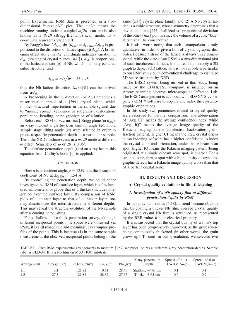
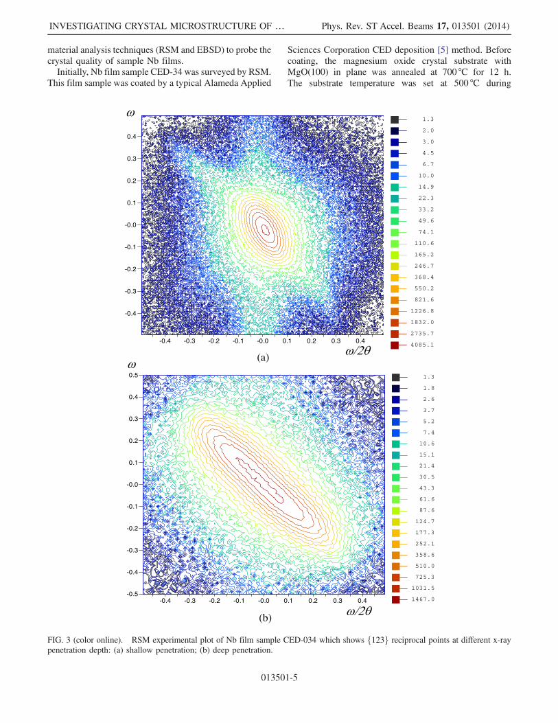
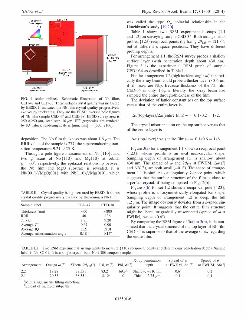
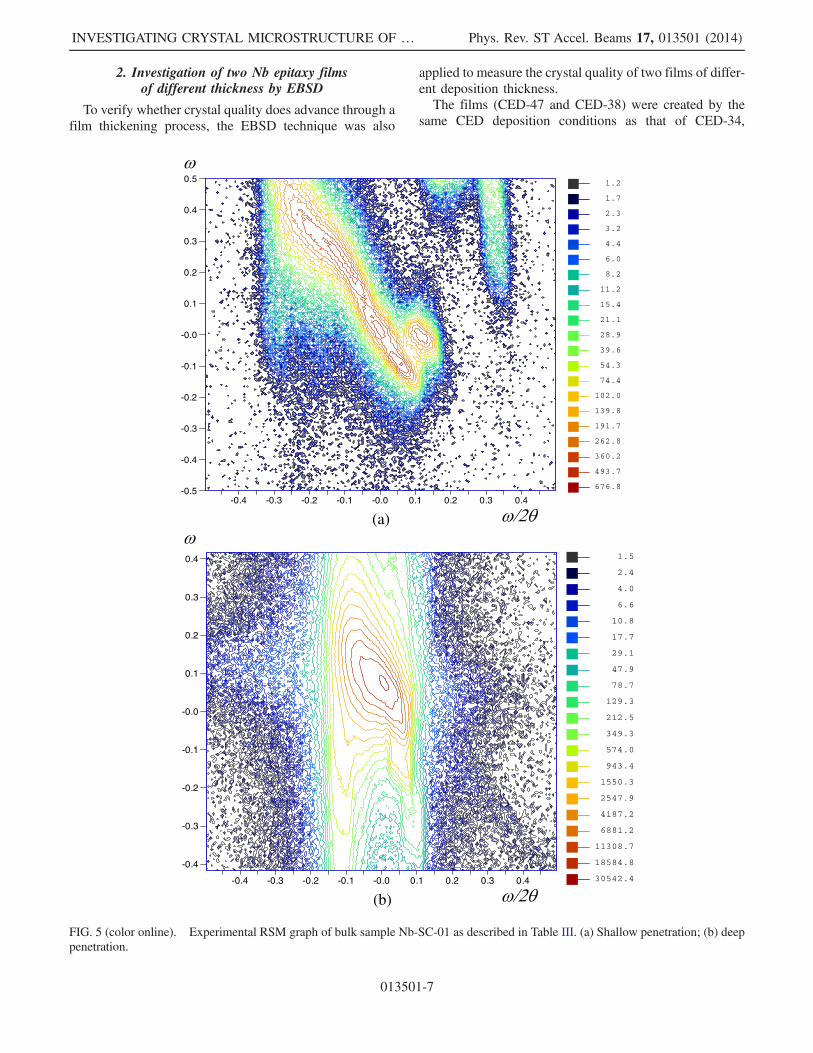