Physics of Materials: Introductiontiiciiitm.com › profanurag › Physics-Class ›...
17
Crystal Physics ABV- IIITM-Gwalior (MP) India Physics of Materials: Introduction It is evident that many years of research by a great many people, both before and after the discovery of the transistor effect, has been required to bring our knowledge of semiconductors to its present development. We were fortunate to be involved at a particularly opportune time and to add another small step in the control of Nature for the benefit of mankind. - John Bardeen, 1956 Nobel lecture
Transcript of Physics of Materials: Introductiontiiciiitm.com › profanurag › Physics-Class ›...

Crystal Physics ABV- IIITM-Gwalior (MP) India
Physics of Materials:
Introduction
It is evident that many years of research by a great many people, both before and
after the discovery of the transistor effect, has been required to bring our
knowledge of semiconductors to its present development. We were fortunate to be
involved at a particularly opportune time and to add another small step in the
control of Nature for the benefit of mankind.
- John Bardeen, 1956 Nobel lecture

Crystal Physics
Dr. Anurag SrivastavaAtal Bihari Vajpayee
Indian Institute of Information Technology and
Management, Gwalior
ABV- IIITM-Gwalior (MP) IndiaCrystal Physics
A presentation of eSyst.org
Electronic Materials
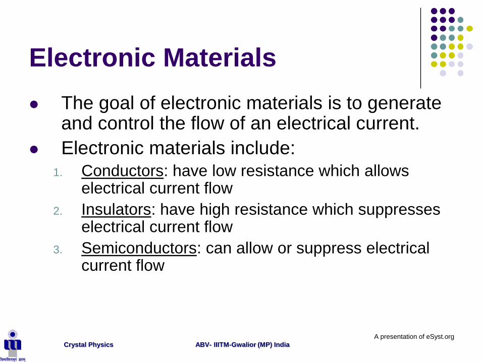
The goal of electronic materials is to generate and control the flow of an electrical current.
Electronic materials include:1. Conductors: have low resistance which allows
electrical current flow
2. Insulators: have high resistance which suppresses electrical current flow
3. Semiconductors: can allow or suppress electrical current flow
ABV- IIITM-Gwalior (MP) IndiaCrystal Physics
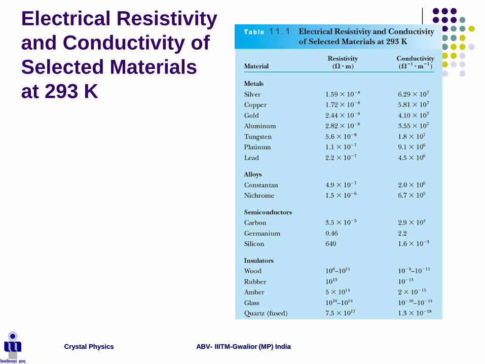
Electrical Resistivity
and Conductivity of
Selected Materials
at 293 K

ABV- IIITM-Gwalior (MP) IndiaCrystal Physics
Reviewing the previous table
reveals that: The electrical conductivity at room temperature is
quite different for each of these three kinds of solids
Metals and alloys have the highest conductivities
followed by semiconductors
and then by insulators
ABV- IIITM-Gwalior (MP) IndiaCrystal Physics

ABV- IIITM-Gwalior (MP) IndiaCrystal Physics
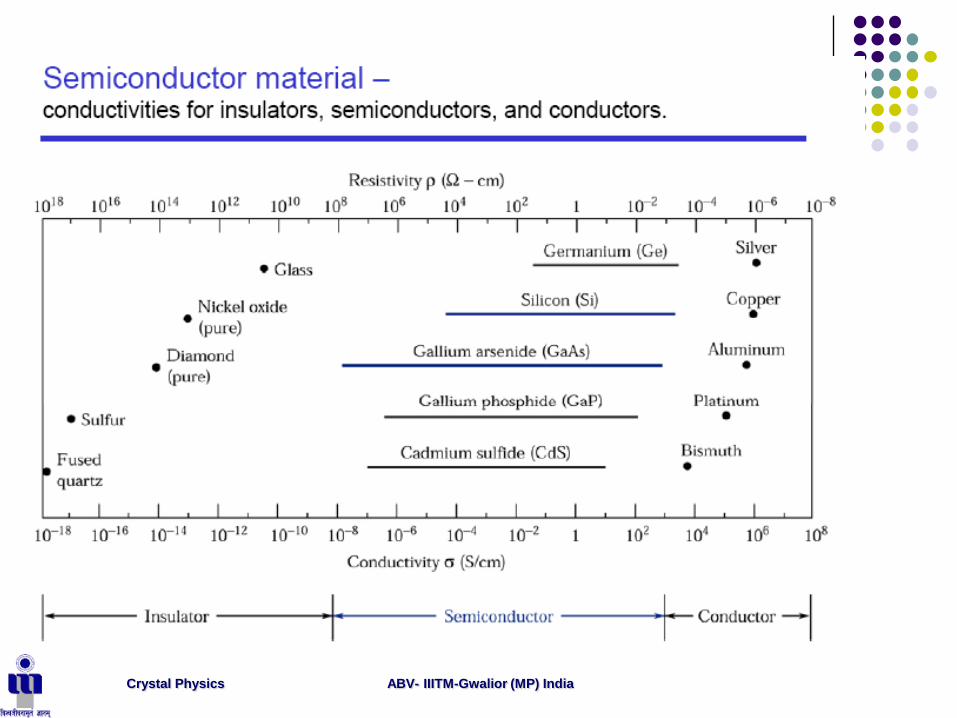
Semiconductor Conduction The free-electron model from Physics does not apply
to semiconductors and insulators, since these
materials simply lack enough free electrons to conduct
in a free-electron mode.
There is a different conduction mechanism for
semiconductors than for normal conductors.
ABV- IIITM-Gwalior (MP) IndiaCrystal Physics
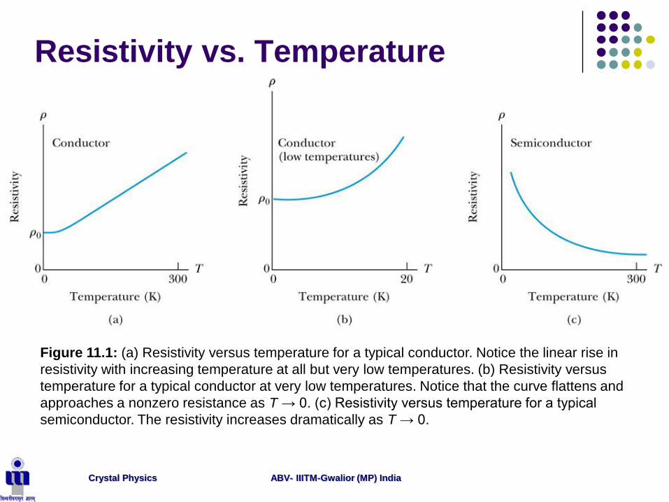
Resistivity vs. Temperature
Figure 11.1: (a) Resistivity versus temperature for a typical conductor. Notice the linear rise in
resistivity with increasing temperature at all but very low temperatures. (b) Resistivity versus
temperature for a typical conductor at very low temperatures. Notice that the curve flattens and
approaches a nonzero resistance as T → 0. (c) Resistivity versus temperature for a typical
semiconductor. The resistivity increases dramatically as T → 0.

ABV- IIITM-Gwalior (MP) IndiaCrystal Physics
Resistance Effects of Doping
If you use lots of arsenic atoms for doping, there will be lots of extra electrons so the resistance of the material will be low and current will flow freely.
If you use only a few boron atoms, there will be fewer free electrons so the resistance will be high and less current will flow.
By controlling the doping amount, virtually any resistance can be achieved.
ABV- IIITM-Gwalior (MP) IndiaCrystal Physics
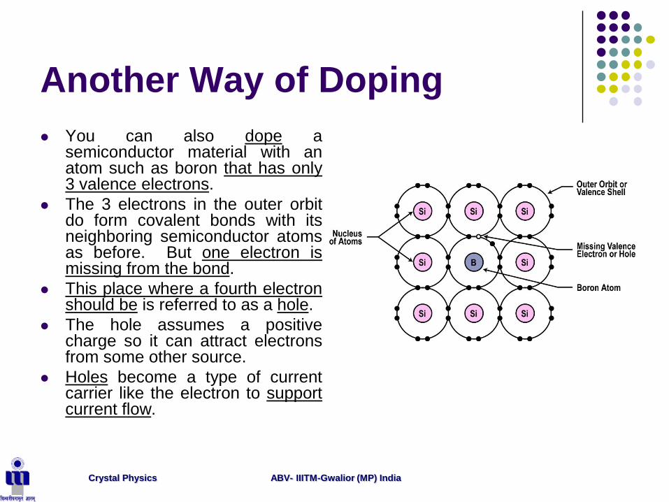
Another Way of Doping
You can also dope asemiconductor material with anatom such as boron that has only3 valence electrons.
The 3 electrons in the outer orbitdo form covalent bonds with itsneighboring semiconductor atomsas before. But one electron ismissing from the bond.
This place where a fourth electronshould be is referred to as a hole.
The hole assumes a positivecharge so it can attract electronsfrom some other source.
Holes become a type of currentcarrier like the electron to supportcurrent flow.

ABV- IIITM-Gwalior (MP) IndiaCrystal Physics

ABV- IIITM-Gwalior (MP) IndiaCrystal Physics
ABV- IIITM-Gwalior (MP) IndiaCrystal Physics

ABV- IIITM-Gwalior (MP) IndiaCrystal Physics
ABV- IIITM-Gwalior (MP) IndiaCrystal Physics
ABV- IIITM-Gwalior (MP) IndiaCrystal Physics
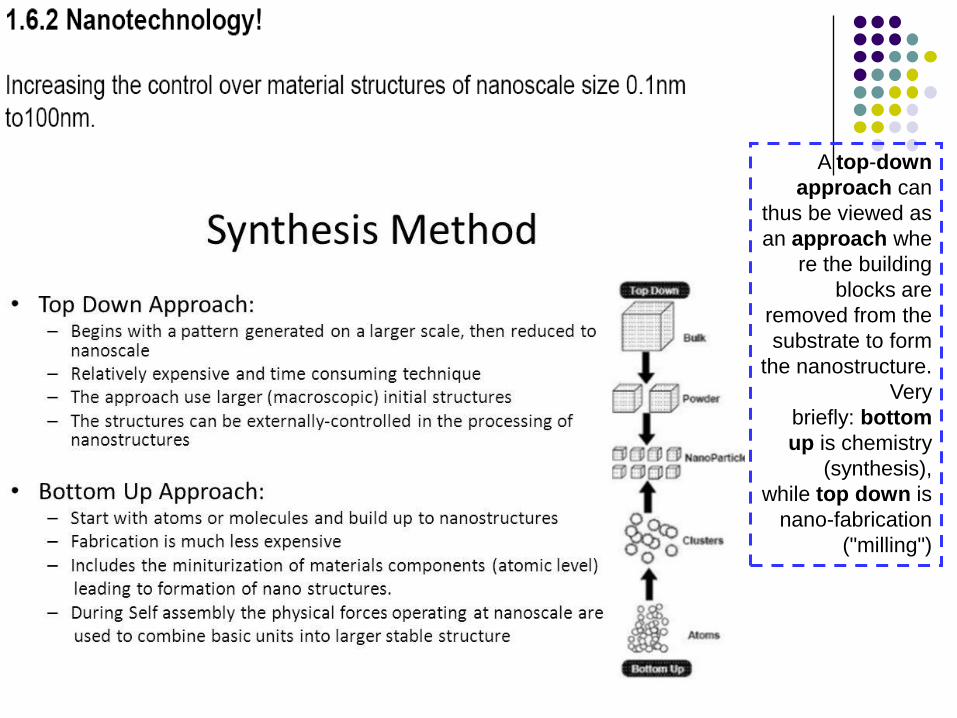
A top-down
approach can
thus be viewed as
an approach whe
re the building
blocks are
removed from the
substrate to form
the nanostructure.
Very
briefly: bottom
up is chemistry
(synthesis),
while top down is
nano-fabrication
("milling")

ABV- IIITM-Gwalior (MP) IndiaCrystal Physics