Photoemission study of the electronic Na Ti Sb
6
Photoemission study of the electronic structure and charge density waves of Na 2 Ti 2 Sb 2 O S. Y. Tan 1,2 , J. Jiang 2,3 , Z. R. Ye 2 , X. H. Niu 2,3 , Y. Song 4 , C. L. Zhang 4,5 , P. C. Dai 4 , B. P. Xie 2,3 , X. C. Lai 1 & D. L. Feng 2,3 1 Science and Technology on Surface Physics and Chemistry Laboratory, Mianyang 621907, China, 2 Physics Department, Applied Surface Physics State Key Laboratory, and Advanced Materials Laboratory, Fudan University, Shanghai 200433, China, 3 Collaborative Innovation Center of Advanced Microstructures, Nanjing University, Nanjing 210093, China, 4 Department of Physics and Astronomy, Rice University, Houston, Texas 77005, USA, 5 Department of Physics and Astronomy, The University of Tennessee, Knoxville, Tennessee 37996-1200, USA. The electronic structure of Na 2 Ti 2 Sb 2 O single crystal is studied by photon energy and polarization dependent angle-resolved photoemission spectroscopy (ARPES). The obtained band structure and Fermi surface agree well with the band structure calculation of Na 2 Ti 2 Sb 2 O in the non-magnetic state, which indicates that there is no magnetic order in Na 2 Ti 2 Sb 2 O and the electronic correlation is weak. Polarization dependent ARPES results suggest the multi-band and multi-orbital nature of Na 2 Ti 2 Sb 2 O. Photon energy dependent ARPES results suggest that the electronic structure of Na 2 Ti 2 Sb 2 O is rather two-dimensional. Moreover, we find a density wave energy gap forms below the transition temperature and reaches 65 meV at 7 K, indicating that Na 2 Ti 2 Sb 2 O is likely a weakly correlated CDW material in the strong electron-phonon interaction regime. L ayered compounds of transition-metal elements always show interesting and novel electric and magnetic properties and have been studied extensively. The discovery of basic superconducting layers, such as the CuO 2 plane 1 in cuprates and Fe 2 An 2 (An 5 P, As, S, Se, Te) layers 2 in iron based superconductors, have opened new fields in physics and chemistry of layered superconductors. Recently another class of layered compounds built from alternatively stacking of special conducting octahedral layers Ti 2 Pn 2 O (Pn5Sb, As) and certain charge reservoir layers [e.g., Na 2 , Ba, (SrF) 2 , (SmO) 2 ] have attracted much attention 3–17 . Most notably, these compounds exhibit competing phases just like in cuprates and iron based superconductors. Both experi- ments and band calculations show that the ground states of Na Ti Sb O (Refs. 6, 9, 18 2 2 2 2 2 12, 13, 20, 21) are possible spin-density wave (SDW) or charge-density wave (CDW) phases, and the Na 1 substitution of Ba 21 in Na x Ba 1-x Ti 2 Sb 2 O suppresses the CDW/SDW, and leads to superconductivity, whose critical temperature (Tc) can be as high as 5.5 K for x50.15 (Refs. 13). These layered compounds provide a new platform to study unconventional superconductivity. Na 2 Ti 2 Sb 2 O is a sister compound to BaTi 2 Sb 2 O, which shows a phase transition at Ts,115 K as characterized by a sharp jump in resistivity and a drop in spin susceptibility 3 . The microscopic mechanism for this phase transition has not been determined, but it has been suggested to arise from the SDW or CDW instability driven by the strongly nested electron and hole Fermi surfaces (Refs. 18–23). However, the nature of the phase transition and its correlation with the superconductivity are still unknown. A recent DFT calculation 23 predicted possible SDW instabilities in Na 2 Ti 2 Pn 2 O (Pn5As, Sb), and more specifically that the ground states of Na 2 Ti 2 Sb 2 O and Na 2 Ti 2 As 2 O are bi-collinear antiferromagnetic semimetal and novel blocked checkerboard antiferromagnetic semiconductor, respectively. An optical study 24 reveals a significant spectral change across the phase transition and the formation of a density-wave-like energy gap. However, one cannot distinguish whether the ordered state is CDW or SDW since both states have the same coherent factor. To date, the experimental electronic structure of Na 2 Ti 2 Sb 2 O has not been reported, which is critical for understanding the nature of the density waves in these compounds. In this article, we investigate the electronic structure of Na 2 Ti 2 Sb 2 O with angle-resolved photoemission spectroscopy (ARPES). Our polarization and photon energy dependent studies reveal the multi-orbital and weak three-dimensional nature of this material. The obtained band structure and Fermi surface agree well with the OPEN SUBJECT AREAS: SUPERCONDUCTING PROPERTIES AND MATERIALS SURFACES, INTERFACES AND THIN FILMS Received 13 December 2014 Accepted 2 March 2015 Published Correspondence and requests for materials should be addressed to D.L.F. (dlfeng@fudan. edu.cn) SCIENTIFIC REPORTS | 5 : 9515 | DOI: 10.1038/srep09515 1 30 April 2015 ,19) and BaTi Sb O (Refs.
Transcript of Photoemission study of the electronic Na Ti Sb

Photoemission study of the electronicstructure and charge density waves ofNa2Ti2Sb2OS. Y. Tan1,2, J. Jiang2,3, Z. R. Ye2, X. H. Niu2,3, Y. Song4, C. L. Zhang4,5, P. C. Dai4, B. P. Xie2,3, X. C. Lai1
& D. L. Feng2,3
1Science and Technology on Surface Physics and Chemistry Laboratory, Mianyang 621907, China, 2Physics Department, AppliedSurface Physics State Key Laboratory, and Advanced Materials Laboratory, Fudan University, Shanghai 200433, China,3Collaborative Innovation Center of Advanced Microstructures, Nanjing University, Nanjing 210093, China, 4Department ofPhysics and Astronomy, Rice University, Houston, Texas 77005, USA, 5Department of Physics and Astronomy, The University ofTennessee, Knoxville, Tennessee 37996-1200, USA.
The electronic structure of Na2Ti2Sb2O single crystal is studied by photon energy and polarizationdependent angle-resolved photoemission spectroscopy (ARPES). The obtained band structure and Fermisurface agree well with the band structure calculation of Na2Ti2Sb2O in the non-magnetic state, whichindicates that there is no magnetic order in Na2Ti2Sb2O and the electronic correlation is weak. Polarizationdependent ARPES results suggest the multi-band and multi-orbital nature of Na2Ti2Sb2O. Photon energydependent ARPES results suggest that the electronic structure of Na2Ti2Sb2O is rather two-dimensional.Moreover, we find a density wave energy gap forms below the transition temperature and reaches 65 meV at7 K, indicating that Na2Ti2Sb2O is likely a weakly correlated CDWmaterial in the strong electron-phononinteraction regime.
L ayered compounds of transition-metal elements always show interesting and novel electric and magneticproperties and have been studied extensively. The discovery of basic superconducting layers, such as theCuO2 plane1 in cuprates and Fe2An2 (An 5 P, As, S, Se, Te) layers2 in iron based superconductors, have
opened new fields in physics and chemistry of layered superconductors. Recently another class of layeredcompounds built from alternatively stacking of special conducting octahedral layers Ti2Pn2O (Pn5Sb, As)and certain charge reservoir layers [e.g., Na2, Ba, (SrF)2, (SmO)2] have attractedmuch attention3–17. Most notably,these compounds exhibit competing phases just like in cuprates and iron based superconductors. Both experi-ments and band calculations show that the ground states of Na Ti Sb O (Refs. 6, 9, 182 2 2 2 2
12, 13, 20, 21) are possible spin-density wave (SDW) or charge-density wave (CDW) phases, and the Na1
substitution of Ba21 in NaxBa1-xTi2Sb2O suppresses the CDW/SDW, and leads to superconductivity, whosecritical temperature (Tc) can be as high as 5.5 K for x50.15 (Refs. 13). These layered compounds provide anew platform to study unconventional superconductivity.
Na2Ti2Sb2O is a sister compound to BaTi2Sb2O, which shows a phase transition at Ts,115 K as characterizedby a sharp jump in resistivity and a drop in spin susceptibility3. The microscopic mechanism for this phasetransition has not been determined, but it has been suggested to arise from the SDWorCDW instability driven bythe strongly nested electron and hole Fermi surfaces (Refs. 18–23). However, the nature of the phase transitionand its correlation with the superconductivity are still unknown. A recent DFT calculation23 predicted possibleSDW instabilities in Na2Ti2Pn2O (Pn5As, Sb), and more specifically that the ground states of Na2Ti2Sb2O andNa2Ti2As2O are bi-collinear antiferromagnetic semimetal and novel blocked checkerboard antiferromagneticsemiconductor, respectively. An optical study24 reveals a significant spectral change across the phase transitionand the formation of a density-wave-like energy gap. However, one cannot distinguish whether the ordered stateis CDWor SDW since both states have the same coherent factor. To date, the experimental electronic structure ofNa2Ti2Sb2O has not been reported, which is critical for understanding the nature of the density waves in thesecompounds.
In this article, we investigate the electronic structure of Na2Ti2Sb2O with angle-resolved photoemissionspectroscopy (ARPES). Our polarization and photon energy dependent studies reveal the multi-orbital and weakthree-dimensional nature of this material. The obtained band structure and Fermi surface agree well with the
OPEN
SUBJECT AREAS:
SUPERCONDUCTINGPROPERTIES AND
MATERIALS
SURFACES, INTERFACES ANDTHIN FILMS
Received13 December 2014
Accepted2 March 2015
Published
Correspondence andrequests for materials
should be addressed toD.L.F. (dlfeng@fudan.
edu.cn)
SCIENTIFIC REPORTS | 5 : 9515 | DOI: 10.1038/srep09515 1
30 April 2015
,19) and BaTi Sb O (Refs.

band structure calculation of Na2Ti2Sb2O in the non-magnetic state,which indicates that there is no magnetic order in Na2Ti2Sb2O andthe electronic correlation is weak. Temperature dependent ARPESresults reveal that a density wave energy gap forms below the trans-ition temperature and reaches 65 meV at 7 K, indicating thatNa2Ti2Sb2O is likely a weakly correlated CDWmaterial in the strongelectron-phonon interaction regime.
ResultsBand Structure. The electronic structure of Na2Ti2Sb2O at 15 K ispresented in Fig. 1. Photoemission intensitymaps are integrated overa [EF - 10 meV, EF1 10 meV] window around the Fermi energy (EF)as shown in Figs. 1(a) and 1(b). The azimuth angle of the sample inFig. 1(b) was rotated by 45u compared with in Fig. 1(a), there is subtlespectrum weight difference in the two obtained Fermi surface maps
due to thematrix element effect. The observed Fermi surface consistsof four square-shaped hole pockets (a) centered at X and four similarelectron pockets (c) centered atM. The electronic structure aroundCis more complicated, mainly consists of a diamond-shaped (b) and afour-leaf clover like (b9) electron pockets. The extracted Fermisurface from photoemission intensity map and the theoreticpredicted Fermi surface are shown in Figs. 1(c) and 1(d), whichagree well with each other. The calculated Fermi surface ofNa2Ti2Sb2O in the non-magnetic state was taken from Ref. 23. TheFermi pockets centered at X and M show multiple parallel sections,providing possible Fermi surface nesting condition for density waveinstabilities, as suggested in previous first principle calculations23.The valence band structures of Na2Ti2Sb2O along C-M and C-X
are present in Figs. 1(e1) and 1(f1). The valence band structures agreequalitatively well with the calculations23 in non-magnetic state
ΓX M
Γα β
γ
β′
(a) (b) (c) (d)
-1.5
-1.0
-0.5
0.0
0.5
1.0
-1.0 -0.5 0.0 0.5 1.0
Γ
X
M
kx (Å-1)
-1.0
-0.5
0.0
0.5
1.0
-1.0 -0.5 0.0 0.5 1.0
Γ
M
X
kx (Å-1)
k y (Å
-1)
-4
-3
-2
-1
0
1.51.00.50.0-0.5-4
-3
-2
-1
0
1.00.50.0-0.5-1.0
Γ M Γ X
-0.6
-0.4
-0.2
0.0
1.00.50.0-0.5-1.0-0.6
-0.4
-0.2
0.0
1.51.00.50.0-0.5k// (Å
-1)1.00.50.0-0.5-1.0
αβΓX
k// (Å-1)k// (Å
-1)1.51.00.50.0-0.5
γββ′Γ M
k// (Å-1)
(h1) (h2)(g1) (g2)
δ
(e1) (e2) (f1) (f2)
δ
η
k// (Å-1)
E-E
F(eV
)E
-EF(
eV)
k// (Å-1)
E-E
F(eV
)E
-EF(
eV)
δ
η
-4
-3
-2
-1
0
Γ M Γ X
-4
-3
-2
-1
0
100 eV 100 eV
114 eV
100 eV 100 eV
114 eV
HighLow
High
Low
High
Low
High
Low
High
Low
High
Low
High
Low
HighLow
Figure 1 | The electronic structure of Na2Ti2Sb2O at 15 K. (a) and (b), Photoemission intensity map at EF integrated over a window [EF - 10 meV, EF1
10 meV], data were measured with 100 eV photons energy. (c), The Fermi surface topology extract from (a) and (b). (d), The theoretic predicted
Fermi surface of Na2Ti2Sb2O. (e1–e2), The experiment and theoretic23 valence band structure along C-M direction. (f1–f2), The experiment and
theoretic23 valence band structure along C-X direction. Data were measured with 100 eV photons energy in (e) and (f). (g1–g2), The photoemission
intensity and its second derivative of the intensity plot with respect to energy along C-M direction. (h1–h2), The photoemission intensity and its second
derivative of the intensity plot with respect to energy along C-X direction, data were measured with 114 eV photons energy.
www.nature.com/scientificreports
SCIENTIFIC REPORTS | 5 : 9515 | DOI: 10.1038/srep09515 2

(Figs. 1(e2) and 1(f2)). Taking two distinct bands d and g as exam-ples, the renormalization factors are very close to 1 for both bands,suggesting the weak correlation character of Na2Ti2Sb2O. Figs. 1(g)and (h) show the low energy electronic structure along the C-M andC-X directions together with their second derivative spectrum. Theband structure as indicated by the dashed curves in Figs. 1(g2) and(h2) are resolved by tracking the local minimum locus in the secondderivative of the ARPES intensity plot with respect to energy. A weakbut dispersive electron band can be resolved around M point, itsband bottom locate at the top of a hole-like band d. Two nearlycoincident electron-like bands (b and b9) can be resolved aroundC point at certain photon energy along the C-M direction, whilethere is only one electron-like band b across EF near C along theC-X direction. A hole-like band a crosses EF and forms the square-shaped pockets around X. The overall measured electronic structureof Na2Ti2Sb2O agrees well with the calculations, and the near-unityrenormalization factor suggests that the ground state of Na2Ti2Sb2Ois nonmagnetic and the correlation is weak.
Polarization Dependence. The electronic structure of Na2Ti2Sb2Onear EF is mainly contributed by Ti 3d orbitals, which is similar to thecase of iron based superconductors. We conducted the polarizationdependent photoemission spectroscopy measurement to resolve thepossible multi-orbital nature of Na2Ti2Sb2O. The experimental setupfor polarization-dependent ARPES is shown in Fig. 2(a). Theincident beam and the sample surface normal define a mirrorplane. For the s (or p) experimental geometries, the electric field ofthe incident photons is out of (or in) the mirror plane. The matrixelement for the photoemission process could be described as:
Mkf ,i! Yk
f e:rj jYk
i
D E������
Since the final stateYkf of photoelectrons could be approximated by a
plane wave with its wave vector in the mirror plane, is always evenwith respect to themirror plane in our experimental geometry. In thes (or p) geometry, e:r is odd (or even) with respect to themirror plane.Thus considering the spatial symmetry of the Ti 3d orbitals, when
the analyzer slit is along the high-symmetry directions, thephotoemission intensity of specific even (or odd) component of aband is only detectable with the p (or s) polarized light. For example,with respect to the mirror plane (the xz plane), the even orbitals (dxz,dzz , and dxz{yz ) and the odd orbitals (dxy and dyz) could be onlyobserved in the p and s geometries, respectively.The photoemission intensity plots of Na2Ti2Sb2O along the C-M
and C-X high symmetry directions are shown in Fig. 2. The incidentC1 light is amixture of both the p and s polarizations, so all the bandswith specific orbital can be seen with the C1 incident light. The bband at C is absent in the s polarization along the C-M direction,visible in both polarizations along the C-X direction, which may beattributed to the Ti dxz orbital. The electron band c only shows up onthe s polarization at the M point, exhibiting its odd nature withrespect to the mirror plane, which may be attributed to the dyzand/or dxy orbital. The hole-like band at X point is not as pure, itis visible in the p polarization along the C-X direction, hardly seen inthe s polarization, which may be a mixture of different Ti 3d orbitals.In general, Na2Ti2Sb2O exhibits obvious polarization dependence,which resembles the multi-band and multi-orbital nature of bandstructure of iron pnictide superconductors25.
Kz Dependence. The calculated electronic structure of Na2Ti2Sb2Oshows typical two dimensional character by the nearly kz-independent Fermi surface sheets around the X and M points,while the electronic structure exhibit significant kz dispersion at Cpoint22,23. To study the three-dimensional character of the electronicstructure in Na2Ti2Sb2O, we have conducted the photon energydependent experiment with circularly polarized photons. Themeasured band structures along the two high-symmetry directions(C-M and C-X) with different photon energies are present in Fig. 3.Figs. 3(a) and (d) show the band dispersion and Fermi crossing alongthe C-X direction, where an electron-like band marked as b and ahole-like band marked as a cross the Fermi energy. The Fermicrossings of bands are determined by tracking the peak positionsin the MDCs taken at various photon energies. The Fermicrossings of a and b bands both show weak kz dispersion with a
-0.6
-0.4
-0.2
0.0
1.00.0 1.00.0 1.00.0
-1.0-0.8-0.6-0.4-0.20.0
1.00.0-1.0 1.00.0-1.0 1.00.0-1.0
-0.6
-0.4
-0.2
0.0
αβ β
γβ γΓ M Γ M Γ M
Γ X Γ X Γ X
k// (Å-1)
k// (Å-1)
(c1) (c2) (c3)
(e1) (e2) (e3)
1.00.0-1.0 1.00.0-1.0 1.00.0-1.0k// (Å
-1)
-1.0-0.8-0.6-0.4-0.20.0
(d1) (d2) (d3)
(f1) (f2) (f3)
1.00.0 1.00.0 1.00.0k// (Å
-1)
C+ p s
C+
p s
p s
(a)
p s
(b)
C+
C+
High
Low
High
Low
High
Low
High
Low
#1
#2
XY
Z
E-E
F(eV
)E
-EF(
eV)
E-E
F(eV
)E
-EF(
eV)
XM
Γ #2
#1
Figure 2 | Polarization dependent photoemission data of Na2Ti2Sb2O at 15 K. (a), Experimental setup for polarization-dependent ARPES. (b), The
Brillouin zone of Na2Ti2Sb2O and locations of the momentum cuts. (c1–c3) and (d1–d3), The photoemission intensity and its second derivative of
the intensity plot with respect to energy alongC-M taken withC1, p and s polarized light, respectively. (e1–e3) and (f1–f3), The photoemission intensity
and its second derivative of the intensity plot with respect to energy along C-X taken with C1, p and s polarized light, respectively, data were
measured with 100 eV photons energy.
www.nature.com/scientificreports
SCIENTIFIC REPORTS | 5 : 9515 | DOI: 10.1038/srep09515 3

typical cycle of each 14 eV photon energy. The Fermi momentum ofb reaches its minimum at 90 eV photon energy, then increases withincreasing photon energy, and reaches its maximum at 104 eV. Onthe contrary, the Fermi momentum of a band reaches its maximumand minimum at 90 eV and 104 eV, respectively.Consistent with the measured Fermi surface, there is only one
electron band near C along the C-X direction (labeled as b), whilewe can clearly observe two electron bands along the C-M direction(labeled as b and b9). The Fermi crossings of b and b9 show negligiblephoton energy dependence alongC-M, while the relative intensity ofb and b9 change with photon energy. For instance at 104 eV, the b9intensity is high, while the b intensity is low.With increasing photonenergy, the intensity of b9 decreases while that of b increases, reach-ing their minimum and maximum at 118 eV, respectively. The rela-tive intensity instead of Fermi crossing shows distinct photon energydependence for b and b9. For the c band near the M point, its Fermimomentum shows weak kz dispersion, with the minimum and max-imum at 104 eV and 118 eV, respectively.The theoretic predicted Fermi surface of Na2Ti2Sb2O shows cylin-
der Fermi sheets near M and X and strong kz dependent Fermi sheetnear C22,23, our photoemission data confirmed the two dimensionalcharacter of the electronic structure at X and M. The weak photonenergy dependence of the electronic structure at C is not consistentwith the theoretic calculation, and this discrepancymay be due to thepoor kz resolution of our ARPES experiment in the vacuum ultra-violet photon energy range. It is known that the poor kz resolutionwould largely smear out the dispersive information along kz for afast-dispersive band, as likely observed here.
Formation of the Density Wave Energy Gap. In the conventionalpicture of density wave transition, the formation of electron-holepairs with a nesting wave vector connecting different regions ofFSs would lead to the opening of an energy gap. In charge-densitywave systems such as 2H-TaS2, strong electron–photon interactionscould cause incoherent polaronic spectral lineshape, and large Fermipatches instead of a clear-cut Fermi surface26. Anomaloustemperature dependent spectral weight redistribution and broadlineshape with incoherent character was reported in BaTi2As2O
(Ref. 27), an iso-structural compound of Na2Ti2Sb2O. It was foundthat partial energy gap opens at the Fermi patches, instead of Fermisurface nesting, is responsible for the CDW in BaTi2As2O.The detailed temperature dependence of the low energy electronic
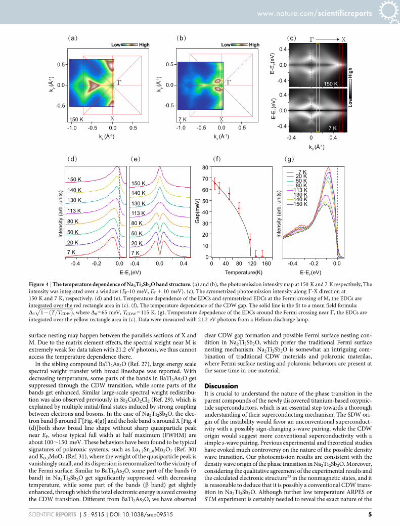
structure of Na2Ti2Sb2O is presented in Fig. 4. The Fermi surfacetopologies of Na2Ti2Sb2O at 150 K and 7 K are rather similar, but adramatic spectra weight change can be observed around the X point.At 150 K, which is above the phase transition temperature 115 K, thespectra weight around X is quite strong compared with those aroundthe C point. At 7 K, which is well below the transition, the spectralweight near X is obviously suppressed, while it was slightly enhancednear C. Fig. 4(c) shows the symmetrized spectrum along C-X. Theband dispersion shows much alike at both temperatures, but anenergy gap opens at X point when it comes into the CDW/SDW stateat 7 K.We tracked the EDCs at the Fermi crossing of a band to revealthe CDW/SDW gap opening behavior more precisely. The densityof states near EF is obviously suppressed with decreasing temperature[Fig. 4(d)]; an energy gap opens at 113 K below the phase transitiontemperature of 115 K for Na2Ti2Sb2O[Fig. 4(e)]. The gap sizeincreased with decreasing temperature, following the typical BCSformula[Fig. 4(f)]. The gap size get saturated at low temperatureand the largest gap size is about 65 meV at 7 K, which give a largeratio of 2D/kBTs,13. The optical study24 revealed 2D/kBTs ,14, inconsistent with our findings. Such a large ratio indicates that thisdensity wave system is in the strong electron–photon couplingregime27.Intriguingly, the photoemission spectrum of the electron band b
around C shows a broad line shape without a sharp quasiparticlepeak near EF, and the spectral weight increases slightly with deceas-ing temperature [Fig. 4(g)]. Furthermore, the peak position movesslightly upward to EF with deceasing temperature. The spectralweight enhancement for b band shows a gradual change behaviorwith decreasing temperature, indicating that it is not relevant to thedensity wave transition around 115 K. Compared with the obviousgap opening behavior at X, it is safe to conclude that the gap does notopen near C. In consideration of the theoretic prediction that X andM show multiple parallel sections, it is nature to deduce that Fermi
Figure 3 | Photon energy dependence of the band structure of Na2Ti2Sb2O at 15 K. (a), Photoemission intensity alongC-X taken with 114 eV photons
[cut #1 in (c)]. (b), Photoemission intensity along C-M with 114 eV photon [cut #2 in (c)]. (c), The Brillouin zone of Na2Ti2Sb2O and the experimental
momentum cuts. (d), Photon energy dependence of the MDCs along C-X. (e), Photon energy dependence of the MDCs along C-M.
www.nature.com/scientificreports
SCIENTIFIC REPORTS | 5 : 9515 | DOI: 10.1038/srep09515 4
surface nesting may happen between the parallels sections of X andM. Due to the matrix element effects, the spectral weight near M isextremely weak for data taken with 21.2 eV photons, we thus cannotaccess the temperature dependence there.In the sibling compound BaTi2As2O (Ref. 27), large energy scale
spectral weight transfer with broad lineshape was reported. Withdecreasing temperature, some parts of the bands in BaTi2As2O getsuppressed through the CDW transition, while some parts of thebands get enhanced. Similar large-scale spectral weight redistribu-tion was also observed previously in Sr2CuO2Cl2 (Ref. 29), which isexplained by multiple initial/final states induced by strong couplingbetween electrons and bosons. In the case of Na2Ti2Sb2O, the elec-tron band b aroundC[Fig. 4(g)] and the hole band a around X [Fig. 4(d)]both show broad line shape without sharp quasiparticle peaknear EF, whose typical full width at half maximum (FWHM) areabout 100,150 meV. These behaviors have been found to be typicalsignatures of polaronic systems, such as La1.2Sr1.8Mn2O7 (Ref. 30)and K0.3MoO3 (Ref. 31), where the weight of the quasiparticle peak isvanishingly small, and its dispersion is renormalized to the vicinity ofthe Fermi surface. Similar to BaTi2As2O, some part of the bands (aband) in Na2Ti2Sb2O get significantly suppressed with decreasingtemperature, while some part of the bands (b band) get slightlyenhanced, throughwhich the total electronic energy is saved crossingthe CDW transition. Different from BaTi2As2O, we have observed
clear CDW gap formation and possible Fermi surface nesting con-dition in Na2Ti2Sb2O, which prefer the traditional Fermi surfacenesting mechanism. Na2Ti2Sb2O is somewhat an intriguing com-bination of traditional CDW materials and polaronic materilas,where Fermi surface nesting and polaronic behaviors are present atthe same time in one material.
DiscussionIt is crucial to understand the nature of the phase transition in theparent compounds of the newly discovered titanium-based oxypnic-tide superconductors, which is an essential step towards a thoroughunderstanding of their superconducting mechanism. The SDW ori-gin of the instability would favor an unconventional superconduct-ivity with a possibly sign-changing s-wave pairing, while the CDWorigin would suggest more conventional superconductivity with asimple s-wave pairing. Previous experimental and theoretical studieshave evoked much controversy on the nature of the possible densitywave transition. Our photoemission results are consistent with thedensity wave origin of the phase transition inNa2Ti2Sb2O.Moreover,considering the qualitative agreement of the experimental results andthe calculated electronic structure23 in the nonmagnetic states, and itis reasonable to deduce that it is possibly a conventional CDW trans-ition in Na2Ti2Sb2O. Although further low temperature ARPES orSTM experiment is certainly needed to reveal the exact nature of the
Figure 4 | The temperature dependence of Na2Ti2Sb2O band structure. (a) and (b), the photoemission intensity map at 150 K and 7 K respectively, The
intensity was integrated over a window (EF-10 meV, EF 1 10 meV). (c), The symmetrized photoemission intensity along C-X direction at
150 K and 7 K, respectively. (d) and (e), Temperature dependence of the EDCs and symmetrized EDCs at the Fermi crossing of M, the EDCs are
integrated over the red rectangle area in (c). (f), The temperature dependence of the CDW gap. The solid line is the fit to a mean field formula:
D0
ffiffiffiffiffiffiffiffiffiffiffiffiffiffiffiffiffiffiffiffiffiffiffiffiffiffiffiffi1{ T=TCDWð Þ
p, where D0565 meV, TCDW5115 K. (g), Temperature dependence of the EDCs around the Fermi crossing near C, the EDCs are
integrated over the yellow rectangle area in (c). Data were measured with 21.2 eV photons from a Helium discharge lamp.
www.nature.com/scientificreports
SCIENTIFIC REPORTS | 5 : 9515 | DOI: 10.1038/srep09515 5

superconducting samples, one can speculate that the superconduct-ivity in NaxBa1-xTi2Sb2O (Ref. 13) is likely due to electron phononinteractions, just like in NbSe2 (Ref. 28).In summary, our experimental band structure agrees qualitatively
well with the calculation23 in the nonmagnetic state, excluding theexistence of possible magnetic order in Na2Ti2Sb2O. Na2Ti2Sb2Oshows obvious multi-band and multi orbital nature, which resemblethe iron-based superconductors. The electron band atM and the holeband at X show weak kz dispersion, consistent with its layered crystalstructure. We observe a large density wave gap of 65 meV whichforms near the X point at 7 K, indicating that Na2Ti2Sb2O is likelya CDW material. The weak renormalization of the overall bandstructure indicates weak electron-electron correlation, while thebroad lineshape and large energy gap and spectral weight transfersuggest the system is likely in the strong electron-phonon interactionregime.
MethodsSample synthesis. Single crystals of Na2Ti2Sb2O were synthesized by the self-fluxmethod. Amixture of Na, Sb, Ti and Ti2O3 withmolar ratio of 185185154 is preparedand put into an aluminum oxide crucible sealed inside a Ta tube. The mixture isgradually heated to 800uC and quenched to room temperature. Afterwards themixture is heated at 1100uC for 2 hours and cooled to 500uC at 5uC/hour beforequenched to room temperature.
ARPES measurement. The polarization and photon energy dependent ARPES datawere taken at the surface and interface spectroscopy beamline of the Swiss LightSource (SLS). The temperature dependent ARPES data were taken with an in-housesetup at Fudan University. All data were collected with Scienta R4000 electronanalyzers. The overall energy resolutionwas 15 meV or better, and the typical angularresolution was 0.3u. The samples were cleaved in-situ and measured under ultrahighvacuum better than 3 3 10211 mbar.
1. Bednorz, J. G. & Muller, K. A. Possible high Tc superconductivity in the Ba-La-Cu-O system. Z. Phys. B. 64, 189–193 (1986).
2. Kamihara, Y. et al. Iron-Based Layered Superconductor La(O1-xFx) FeAs(x50.0520.12) with Tc 5 26 K. J. Am. Chem. Soc. 130, 3296–3297 (2008).
3. Adam, A. & Schuster, H.-U. Darstellung und Kristallstruktur der PnictidoxideNa2Ti2As2O und Na2Ti2Sb2O. Z. Anorg. Allg. Chem. 584, 150–158 (1990).
4. Axtell, E. A. et al. Phase Transition and Spin-gap Behavior in a Layered TetragonalPnictide Oxide. J. Solid State Chem. 134, 423–426 (1997).
5. Ozawa, T. C. et al. Powder Neutron Diffraction Studies of Na2Ti2Sb2O and ItsStructure–Property Relationships. J. Solid State Chem. 153, 275–281 (2000).
6. Ozawa, T. et al. Possible Charge-Density-Wave/Spin-Density-Wave in theLayered Pnictide2Oxides: Na2Ti2Pn2O (Pn 5 As, Sb). Chem. Mat. 13,1804–1810 (2001).
7. Ozawa, T. C. & Kauzlarich, S. M. Single crystal growth and characterization of alayered transition metal pnictide oxide: Na2Ti2Sb2O. J. Cryst. Growth. 265,571–576 (2004).
8. Ozawa, T. C. &Kauzlarich, S.M. Chemistry of layeredd-metal pnictide oxides andtheir potential as candidates for new superconductors. Sci. Technol. Adv.Mater. 9,033003 (2008).
9. Liu, R. H. et al. Physical properties of the layered pnictide oxides Na2Ti2P2O(P5As, Sb). Phys. Rev. B 80, 144516 (2009).
10. Wang, X. F. et al. Structure and physical properties for a new layered pnictide-oxide: BaTi2As2O. J. Phys. Condens. Matter. 22, 075702 (2010).
11. Liu, R. H. et al. Structure and Physical Properties of the Layered Pnictide-Oxides:(SrF)2Ti2Pn2O (Pn 5 As, Sb) and (SmO)2Ti2Sb2O. Chem. Mat. 22, 1503–1508(2010).
12. Yajima, T. et al. Superconductivity in BaTi2Sb2O with a d1 Square Lattice. J. Phys.Soc. Jpn. 81, 103706 (2012).
13. Doan, P. et al. Ba1-xNaxTi2Sb2O (0.0 # x # 0.33): A Layered Titanium-BasedPnictide Oxide Superconductor. J. Am. Chem. Soc. 134, 16520–16523 (2012).
14. Gooch, M. et al. Weak coupling BCS-like superconductivity in the pnictide oxideBa12xNaxTi2Sb2O (x50 and 0.15). Phys. Rev. B 88, 064510 (2013).
15. Litvinchuk, A. P. et al. Lattice dynamics of Ti-based pnictide superconductorsBa12xNaxTi2Sb2O. Phys. Rev. B 87, 064505 (2013).
16. Von Rohr, F. et al. Conventional superconductivity and charge-density-waveordering in Ba12xNaxTi2Sb2O. Phys. Rev. B 88, 140501 (2013).
17. Zhai, H.-F. et al. Superconductivity, charge- or spin-density wave, and metal-nonmetal transition in BaTi2(Sb12xBix)2O. Phys. Rev. B. 87, 100502 (2013).
18. Biani, F. F. D. et al. Concerning the Resistivity Anomaly in the Layered PnictideOxide Na2Ti2Sb2O. Inorg. Chem. 37, 5807–5810 (1998).
19. Pickett, W. E. Electronic instability in inverse-K2NiF4-structure Na2Ti2Sb2O.Phys. Rev. B 58, 4335–4340 (1998).
20. Singh, D. J. Electronic structure, disconnected Fermi surfaces andantiferromagnetism in the layered pnictide superconductor NaxBa12xTi2Sb2O.New J. Phys. 14, 123003 (2012).
21. Subedi, A. Electron-phonon superconductivity and charge density waveinstability in the layered titanium-based pnictide BaTi2Sb2O. Phys. Rev. B 87,054506 (2013).
22. Suetin, D. V. & Ivanovskii, A. L. Structural, electronic properties, and chemicalbonding in quaternary layered titanium pnictide-oxides Na2Ti2Pn2O andBaTi2Pn2O (Pn5As, Sb) from FLAPW–GGA calculations. J. Alloy. Compd. 564,117–124 (2013).
23. Yan, X.-W. & Lu, Z.-Y. Layered pnictide-oxide Na2Ti2Pn2O (Pn5As, Sb): acandidate for spin density waves. J. Phys-Condens. Mat. 25, 365501 (2013).
24. Huang, Y. et al. Formation of the density wave energy gap in Na2Ti2Sb2O: Anoptical spectroscopy study. Phys. Rev. B 87, 100507 (2013).
25. Zhang, Y. et al. Orbital characters of bands in the iron-based superconductorBaFe1.85Co0.15As2. Phys. Rev. B 83, 054510 (2011).
26. Shen, D. W. et al. Novel Mechanism of a Charge Density Wave in a TransitionMetal Dichalcogenide. Phys. Rev. Lett. 99, 216404 (2007).
27. Xu, H. C. et al. Electronic structure of the BaTi2As2O parent compound of thetitanium-based oxypnictide superconductor. Phys. Rev. B 89, 155108 (2014).
28. Shen, D. W. et al. Primary Role of the Barely Occupied States in the ChargeDensity Wave Formation of NbSe2. Phys. Rev. Lett. 101, 226406 (2008).
29. Kim, C. et al. Anomalous temperature dependence in the photoemission spectralfunction of cuprates. Phys. Rev. B 65, 174516 (2002).
30.Mannella, N. et al. Nodal quasiparticle in pseudogapped colossal magnetoresistivemanganites. Nature 438, 474–478 (2005).
31. Mozos, J. L. et al. First-principles study of the blue bronze K0.3MoO3. Phys. Rev. B65, 233105 (2002).
AcknowledgmentsWe thankDr.M. Shi for the experimental support at Swiss Light Source (SLS).We gratefullyacknowledge helpful discussions with Prof. N. L. Wang. This work is supported in part bythe National Science Foundation of China and the National Basic Research Program ofChina (973 Program) under Grants No. 2012CB921400, No. 2011CB921802,No.2011CBA00112, No. 2011CB309703, andNo. 91026016. The single crystal growth workat the University of Tennessee was supported by the U.S. DOE, BES, through Contract No.DE-FG02-05ER46202.
Author contributionsS.Y.T., J.J., Z.R.Y., X.H.N. and B.P.X. performed the ARPESmeasurements. Y.S., C.L.Z. andP.C.D. provided the single crystal samples. S.Y.T. and D.L.F. analyzed the ARPES data, S.Y.T. and D.L.F. wrote the paper. D.L.F. and X.C.L. are responsible for the infrastrure,projection and planning. All authors reviewed the manuscript.
Additional informationCompeting financial interests: The authors declare no competing financial interests.
How to cite this article: Tan, S.Y. et al. Photoemission study of the electronic structure andcharge density waves of Na2Ti2Sb2O. Sci. Rep. 5, 9515; DOI:10.1038/srep09515 (2015).
This work is licensed under a Creative Commons Attribution 4.0 InternationalLicense. The images or other third party material in this article are included in thearticle’s Creative Commons license, unless indicated otherwise in the credit line; ifthe material is not included under the Creative Commons license, users will needto obtain permission from the license holder in order to reproduce thematerial. Toview a copy of this license, visit http://creativecommons.org/licenses/by/4.0/
www.nature.com/scientificreports
SCIENTIFIC REPORTS | 5 : 9515 | DOI: 10.1038/srep09515 6


![Preparation and Characterization of Ti/SnO2-Sb …cathode for different purposes [15, 19-23]. For Ti/SnO 2-Sb electrodes, platinum has been used as an interlayer or as a doping agent](https://static.fdocuments.us/doc/165x107/5f8a871b1a75284b706152f6/preparation-and-characterization-of-tisno2-sb-cathode-for-different-purposes-15.jpg)