Phase Domain Signal Processing - Carleton University
20
Phase Domain Signal Processing Tad Kwasniewski and Dianyong Chen July 28, 2006
Transcript of Phase Domain Signal Processing - Carleton University

Phase Domain Signal Processing
Tad Kwasniewskiand
Dianyong Chen
July 28, 2006

Phase Domain Signal Processing Tad Kwasniewski and Dianyong Chen#2
Outline
■ Some characteristics of deep sub-micrometer CMOS technologies
■ Advantages of phase domain signal processing■ Examples Phase domain circuits:
– Phase domain all digital phase locked loop (ADPLL)– Self oscillating power amplifier (SOPA)– Oversampling analog-to-digital converter (OSADC)
■ Example of a phase domain signal processing – Edge equalization
■ Conclusion■ Acknowledgement■ Reference
Phase Domain Signal Processing Tad Kwasniewski and Dianyong Chen#3
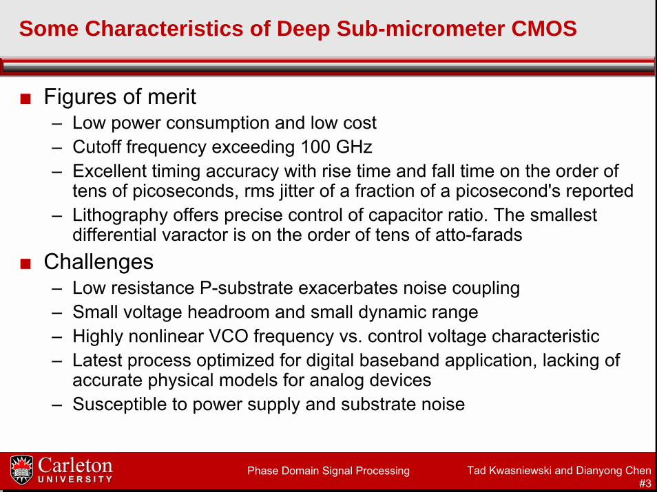
Some Characteristics of Deep Sub-micrometer CMOS
■ Figures of merit– Low power consumption and low cost– Cutoff frequency exceeding 100 GHz– Excellent timing accuracy with rise time and fall time on the order of
tens of picoseconds, rms jitter of a fraction of a picosecond's reported– Lithography offers precise control of capacitor ratio. The smallest
differential varactor is on the order of tens of atto-farads■ Challenges
– Low resistance P-substrate exacerbates noise coupling– Small voltage headroom and small dynamic range – Highly nonlinear VCO frequency vs. control voltage characteristic– Latest process optimized for digital baseband application, lacking of
accurate physical models for analog devices– Susceptible to power supply and substrate noise

Phase Domain Signal Processing Tad Kwasniewski and Dianyong Chen#4
Advantages of Phase Domain Signal Processing
■ Based on new paradigm of design– In deep sub-micrometer CMOS, time resolution is much better than
voltage resolution– Alternative architectures should be able to
• leverage the advantages, and minimize the disadvantages
■ Phase Definition– For periodic signals phase is defined as a deviation of a threshold
crossing point from a position defined by the waveform ideal period– Definition involves two waveforms and a voltage threshold
■ In the following examples phase representation is used to contain amplitude information (through oversampling: delta-sigma ADC, power amplifier) or as a replacement of amplitude domain processing (digital PLL and edge equalization)

Phase Domain Signal Processing Tad Kwasniewski and Dianyong Chen#5
Charge Pump Based PLL
Analog Voltage
■ Linear region of varactor capacitance vs. voltage is smaller in deep sub-micrometer CMOS– High gain (KVCO) leads to susceptibility to noise and operating point
shift
■ Charge pump based PLL relies on analog voltage
[1][1]
Phase Domain Signal Processing Tad Kwasniewski and Dianyong Chen#6
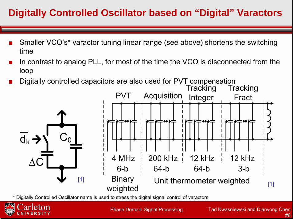
Digitally Controlled Oscillator based on “Digital” Varactors
dk C0
ΔC
■ Smaller VCO’s* varactor tuning linear range (see above) shortens the switching time
■ In contrast to analog PLL, for most of the time the VCO is disconnected from the loop
■ Digitally controlled capacitors are also used for PVT compensation
[1][1]
* Digitally Controlled Oscillator name is used to stress the dig* Digitally Controlled Oscillator name is used to stress the digital signal control of ital signal control of varactorsvaractors
[1][1]
Phase Domain Signal Processing Tad Kwasniewski and Dianyong Chen#7
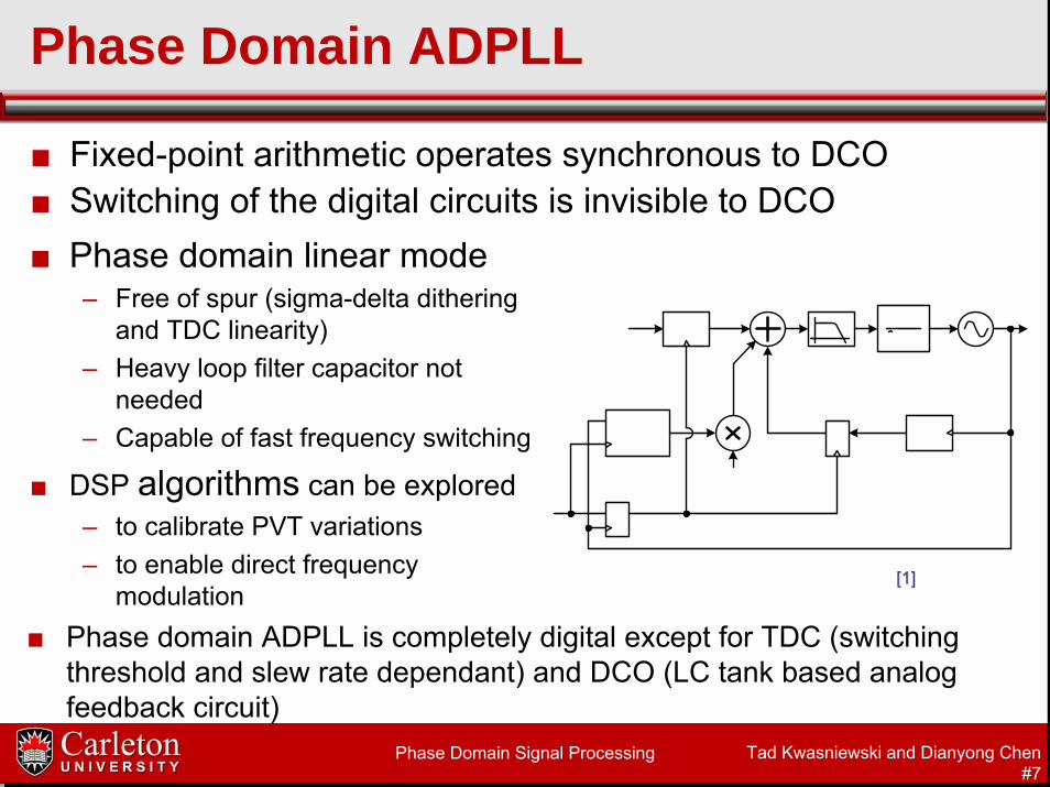
Phase Domain ADPLL
■ Fixed-point arithmetic operates synchronous to DCO ■ Switching of the digital circuits is invisible to DCO■ Phase domain linear mode
– Free of spur (sigma-delta dithering and TDC linearity)
– Heavy loop filter capacitor not needed
– Capable of fast frequency switching
■ DSP algorithms can be explored– to calibrate PVT variations– to enable direct frequency
modulation■ Phase domain ADPLL is completely digital except for TDC (switching
threshold and slew rate dependant) and DCO (LC tank based analogfeedback circuit)
[1][1]

Phase Domain Signal Processing Tad Kwasniewski and Dianyong Chen#8
■ Large tuning range– Tuning range of 500 MHz at 2.4 GHz has been reported
■ Small phase noise– 167 dBc/Hz at 20 MHz offset from 915 MHz has been reported
■ Short settling time– 10 μs settling time for GSM transceiver has been reported
■ Excellent frequency resolution– Frequency resolution of 39 Hz at 2 GHz has been reported
■ Enables RF transceivers be implemented with deep sub-micrometer CMOS technologies optimized for digital baseband applications– Bluetooth, GPRS, and GSM/EDGE Transceivers have been reported
Performance of Phase Domain ADPLL
[1][1]
[3][3]
[4][4]
[5][5]
[6][6]

Phase Domain Signal Processing Tad Kwasniewski and Dianyong Chen#9
Operation of Self-Oscillating Power Amplifier
■ ADSL line driver must meet low-voltage, high linearity, and high power efficiency requirements
[7][7]
Phase Domain Signal Processing Tad Kwasniewski and Dianyong Chen#10
Noise Shaping Technique in SOPA
■ Loop is unstable■ Input signal carried by the phase of limit cycle
oscillation waveform– The limit cycle oscillation creates a binary signal; pulse
density (as in delta-sigma ADC) represents the analog voltage
■ Noise shaping suppresses harmonic distortion and noise
■ SOPA can be viewed as a class D power amplifier with high efficiency
■ Dithering can further improve linearity■ Differential (cross coupling) signal techniques can
be used to reduce harmonics

Phase Domain Signal Processing Tad Kwasniewski and Dianyong Chen#11
Performance of Phase Domain SOPA
■ A 0.35 μm CMOS Implementation [8] yields– Crest factor: >5– Bandwidth: 8.6
MHz– MTPR: 56 dB– Power supply: 3.3
V– Total Efficiency:
>47%– Area: 6.76 mm2
– Output power: 21.1 dBm
[8][8] INPUT OUTPUTINPUT OUTPUT
Simulation results obtained by authorsSimulation results obtained by authors

Phase Domain Signal Processing Tad Kwasniewski and Dianyong Chen#12
Oversampling ADC
■ Oversampling ADC shares the design rationale with SOPA– Input signal is converted into phase domain (binary output
– signal represented by pulse density)– Noise shaping pushes quantization noise and harmonic
distortion components outside of the signal band ■ Oversampling ADC is a clocked phase domain
signal processing system– Able to exploit more sophisticated DSP algorithms

Phase Domain Signal Processing Tad Kwasniewski and Dianyong Chen#13
Channel Properties of High-speed Serial Link
■ Transmission over a multi-gigahertz backplane channel suffers from loss and dispersion
■ Conventional center equalization results in incomplete canceling of ISI induced zero crossing jitter

Phase Domain Signal Processing Tad Kwasniewski and Dianyong Chen#14
Edge Equalization
■ Error free data recovery relies on– Eliminated or minimized inter-symbol-interference (ISI)– Correct sampling phase
■ In high-speed serial link– Eye opening becomes narrower due to jitter caused by ISI
■ Edge equalization aims to eliminate ISI to the sampling phase– Leaves controlled amplitude ISI at sampling point
Center equalized NRZ eye pattern
Edge equalized NRZ eye pattern

Phase Domain Signal Processing Tad Kwasniewski and Dianyong Chen#15
Edge Equalization in Multi-Gigabit Serial Links
■ Target Response is aimed to eliminate clock (sampling phase) ISI■ Edge equalization needs less frequency bandwidth and less boost than
center equalization
[9][9]
[9][9]
TxTx EqualizerEqualizer
RxRx

Phase Domain Signal Processing Tad Kwasniewski and Dianyong Chen#16
Bit Detection for Edge Equalized Signal
■ The edge equalized NRZ signal can be sampled at three points
Edge Equalized NRZ Eye PatternEdge Equalized NRZ Eye Pattern
Possible sampling pointsPossible sampling points

Phase Domain Signal Processing Tad Kwasniewski and Dianyong Chen#17
12 Gb/s x2 Oversampling Multi-phase Edge Equalization
■ Sampled transition-edge value used for equalizer adaptation■ 2 bit transition for clock recovery■ 3 GHz, 8-phase oversampling
[10][10]

Phase Domain Signal Processing Tad Kwasniewski and Dianyong Chen#18
Conclusions
■ Phase domain signal processing fits the new design paradigm of deep sub-micrometer CMOS techniques very well– Phase domain signals do not rely on fine analog voltage resolution– Phase domain signals do not suffer from voltage headroom– 100+ GHz bandwidth of CMOS devices ensures fast switching, allows
oversampling■ Edge Equalized NRZ Tx signal requires less bandwidth than center
equalized signal■ Reviewed examples utilizing phase domain signal processing show
– Reduced cost• RF SoC using latest CMOS technologies possible
– Low power consumption– Improved system performance– Ability to exploit the power of sophisticated DSP algorithms

Phase Domain Signal Processing Tad Kwasniewski and Dianyong Chen#19
Acknowledgements
Inspiration from Robert B. Staszewski (TI) and Kumar Lakshmikumar (Conexant) is acknowledged.
Support from NSERC, CITO, CMC and AlteraCorporation is gratefully acknowledged.

Phase Domain Signal Processing Tad Kwasniewski and Dianyong Chen#20
Reference1. R.B.Staszewski, “A First Multigigahertz Digitally Controlled Oscillator for Wireless Applications,” IEEE
Transactions on Microwave Theory and Techniques, Vol.51, NO.11, November 2003, pp2154-2164.2. R.B.Staszewski and P.T.Balsara, "Phase-Domain All-Digital Phase-Locked Loop," IEEE Transactions
on Circuits and Systems—II: Express Briefs, Vol. 52, NO. 3, MARCH 2005, pp 159-163.3. C.M.Hung and et al, “A First RF Digitally-Controlled Oscillator for SAW-less TX in Cellular Systems,”
2005 IEEE Symposium on VLSI Circuits Digest of Technical Papers, pp.402-405.4. R.B.Staszewski and et al, “ All-Digital PLL and Transmitter for Mobile Phones”, IEEE JOURNAL OF
SOLID-STATE CIRCUITS, VOL. 40, NO. 12, DECEMBER 2005, pp.2469-2482 5. R.B.Staszewski, C.M.Hung, N.Barton, M.C.Lee, and D.Leipold, "A First RF Digitally-Controlled
Oscillator for Mobile Phones.” IEEE Radio Frequency Integrated Circuits Symposium, 20056. R.B.Staszewski and et al, "All-Digital TX Frequency Synthesizer and Discrete-Time Receiver for
Bluetooth Radio in 130-nm CMOS," IEEE Journal of Solid-State Circuits, Vol. 39, NO. 12, December 2004, pp.2278-2291.
7. Tim Piessens and Michel S. J. Steyaert, “Behavioral Analysis of Self-Oscillating Class D Line Drivers,” IEEE Transactions on Circuits and Systems—I: Regular Papers, Vol. 52, NO. 4, APRIL 2005, pp.706-714.
8. Tim Piessens and Michiel Steyaert, “Highly Efficient xDSL Line Drivers in 0.35 μm CMOS Using a Self-Oscillating Power Amplifier,” IEEE JOURNAL OF SOLID-STATE CIRCUITS, VOL. 38, NO. 1, JANUARY 2003, pp22-29.
9. Brian Brunn and Setve Anderson, "Edge-Equalization Extends Performance in Multi-Gigabit Serial Links." DesignCon 2005.
10. Kouichi Yamaguchi and et al,"12 Gb/s Duobinary Signaling with x2 Oversampling Edge Equalization." ISSCC 2005.