Perpendicular magnetic anisotropy in the Heusler alloy ... · Perpendicular magnetic anisotropy in...
9
Perpendicular magnetic anisotropy in the Heusler alloy Co2TiSi/GaAs(001) hybrid structure M. T. Dau, B. Jenichen, and J. Herfort Citation: AIP Advances 5, 057130 (2015); doi: 10.1063/1.4921237 View online: http://dx.doi.org/10.1063/1.4921237 View Table of Contents: http://scitation.aip.org/content/aip/journal/adva/5/5?ver=pdfcov Published by the AIP Publishing Articles you may be interested in Highly (001) oriented L10-CoPt/TiN multilayer films on glass substrates with perpendicular magnetic anisotropy J. Vac. Sci. Technol. A 33, 021512 (2015); 10.1116/1.4905847 Full-Heusler Co2FeSi alloy thin films with perpendicular magnetic anisotropy induced by MgO-interfaces J. Appl. Phys. 115, 17C732 (2014); 10.1063/1.4865971 Nonlinear strain dependence of magnetic anisotropy in CoFe2O4 films on MgO(001) substrates J. Appl. Phys. 115, 17C101 (2014); 10.1063/1.4853235 Interface effects in highly oriented films of the Heusler alloy Co 2 MnSi on GaAs(001) J. Appl. Phys. 99, 013904 (2006); 10.1063/1.2161417 Perpendicular magnetic anisotropy of Co–TiN composite film with nano-fiber structure J. Appl. Phys. 93, 6273 (2003); 10.1063/1.1567032 All article content, except where otherwise noted, is licensed under a Creative Commons Attribution 3.0 Unported license. See: http://creativecommons.org/licenses/by/3.0/ Downloaded to IP: 62.141.165.1 On: Wed, 13 May 2015 13:56:01
Transcript of Perpendicular magnetic anisotropy in the Heusler alloy ... · Perpendicular magnetic anisotropy in...
Perpendicular magnetic anisotropy in the Heusler alloy Co2TiSi/GaAs(001) hybridstructureM. T. Dau, B. Jenichen, and J. Herfort Citation: AIP Advances 5, 057130 (2015); doi: 10.1063/1.4921237 View online: http://dx.doi.org/10.1063/1.4921237 View Table of Contents: http://scitation.aip.org/content/aip/journal/adva/5/5?ver=pdfcov Published by the AIP Publishing Articles you may be interested in Highly (001) oriented L10-CoPt/TiN multilayer films on glass substrates with perpendicular magneticanisotropy J. Vac. Sci. Technol. A 33, 021512 (2015); 10.1116/1.4905847 Full-Heusler Co2FeSi alloy thin films with perpendicular magnetic anisotropy induced by MgO-interfaces J. Appl. Phys. 115, 17C732 (2014); 10.1063/1.4865971 Nonlinear strain dependence of magnetic anisotropy in CoFe2O4 films on MgO(001) substrates J. Appl. Phys. 115, 17C101 (2014); 10.1063/1.4853235 Interface effects in highly oriented films of the Heusler alloy Co 2 MnSi on GaAs(001) J. Appl. Phys. 99, 013904 (2006); 10.1063/1.2161417 Perpendicular magnetic anisotropy of Co–TiN composite film with nano-fiber structure J. Appl. Phys. 93, 6273 (2003); 10.1063/1.1567032
All article content, except where otherwise noted, is licensed under a Creative Commons Attribution 3.0 Unported license. See:
http://creativecommons.org/licenses/by/3.0/ Downloaded to IP: 62.141.165.1 On: Wed, 13 May 2015 13:56:01
AIP ADVANCES 5, 057130 (2015)
Perpendicular magnetic anisotropy in the Heusler alloyCo2TiSi/ GaAs(001) hybrid structure
M. T. Dau,a B. Jenichen, and J. HerfortPaul-Drude-Institut für Festkörperelektronik, Hausvogteiplatz 5-7, D-10117 Berlin, Germany
(Received 13 March 2015; accepted 5 May 2015; published online 13 May 2015)
Investigation of the thickness dependence of the magnetic anisotropy in B2-typeCo2TiSi films on GaAs(001), shows a pronounced perpendicular magnetic anisotropyat 10 K for thicknesses up to 13.5 nm. We have evidenced that the interfacialanisotropy induced by interface clusters has a strong influence on the perpendicularmagnetic anisotropy of this hybrid structure, especially at temperatures lower thanthe blocking temperature of the clusters (28 K). However, as this influence can beruled out at higher temperatures, the perpendicular magnetic anisotropy which isfound to persist up to room-temperature can be ascribed to the magnetic propertiesof the Co2TiSi films. For thicknesses larger than 15.0 nm, we observe an alignmentof the magnetic easy axis parallel to the sample surface, which is most likely dueto the shape anisotropy and the film structure. C 2015 Author(s). All article content,except where otherwise noted, is licensed under a Creative Commons Attribution 3.0Unported License. [http://dx.doi.org/10.1063/1.4921237]
INTRODUCTION
Perpendicular magnetic anisotropy (PMA) in ferromagnetic films where the easy axis ofmagnetization is oriented out-of-plane, is of great interest for realizing perpendicular magnetictunnel junctions. Such junctions are used in devices with high processing speed and high-densitynon-volatile memory.1–3 In addition, the implementation of perpendicularly magnetized thin films insemiconductor-based spintronic devices, for example, in a spin-light emitting diode (spin-LED) hasbeen recently demonstrated as a potential approach to achieve an efficient transfer of spin-polarizedcurrent into semiconducting channels.4,5 However, those devices suffer from the requirement of alarge applied magnetic field to turn the magnetic moment out of the sample surface.
Ferromagnetic films with PMA are not commonly observed due to the long-range dipolarinteractions or the shape effect. The well-known PMA materials are magnetic alloys containingrare-earth, noble or transition metals. For instance, granular films as well as amorphous filmsbased on CoPt, FePt, CoCr, TbFe exhibit a pronounced PMA.6–9 Nevertheless, potential applica-tions of such materials are limited because of their low crystalline quality. Another widespreadPMA material class is metallic stacking layers that are also based on transition, noble metals andrare-earth magnets.10,11 The PMA of these structures has an interfacial origin for which the orbitalhybridization and/or the intermixing at the interface promotes the perpendicular spin coupling.12,13
Since metallic layers should be thin enough for triggering the PMA, the fabrication process of suchmultilayers and the related devices would be more complicated than a simple layer.
In the last decade, the growth and characterization of full Heusler alloy (FHA) films havebeen intensely investigated because many of them have been theoretically predicted to have afully spin-polarized conduction band.14–17 The intrinsic magnetic anisotropy of the well-knownFHA films has been found to be dominated by the in-plane anisotropy.16–18 Very recently, theinterface-induced PMA was discovered in a Co-based FHA (Co2FeAl) in contact with a MgO oxidelayer.19,20 The proposed explanation for the PMA is similar to that of CoFeB or Fe/MgO systems forwhich interfacial anisotropy induced by hybridization of Fe-, Co-3d and O-2p orbitals causes the
aElectronic email: [email protected]
2158-3226/2015/5(5)/057130/8 5, 057130-1 ©Author(s) 2015
All article content, except where otherwise noted, is licensed under a Creative Commons Attribution 3.0 Unported license. See:
http://creativecommons.org/licenses/by/3.0/ Downloaded to IP: 62.141.165.1 On: Wed, 13 May 2015 13:56:01
057130-2 Dau, Jenichen, and Herfort AIP Advances 5, 057130 (2015)
PMA.3,21 For a hybrid structure based on a very thin FHA film (on the order of a few angstroms)coupled with a MgO barrier, a question is whether chemical interactions will alter the electronicband structure of the FHA, (i. e, its spin polarization). Furthermore, film oxidation arising fromexcess oxygen makes the control of such an interface relatively difficult. Therefore, it is desired toacquire a PMA FHA film with easy-to-adjust thickness in order to maintain its intrinsic high spinpolarization and perpendicular magnetization properties. In this study, we report on the observationof PMA in FHA Co2TiSi/GaAs hybrid structures for thicknesses up to 13.5 nm, which is one orderof magnitude higher than that previously reported for of PMA ultra-thin films.3,19,21 For higherthicknesses, the in-plane magnetic anisotropy dominates and the easy axis of magnetization is thusfound to be in-plane.
EXPERIMENTAL
All the Co2TiSi films were grown on semi-insulating (001)-oriented GaAs substrates. A 400-nm-thick GaAs buffer layer was grown in a III-V semiconductor growth chamber to ensure asingle-crystal surface free of contaminants and defects. The Co2TiSi films were subsequentlysynthesized in an As-free chamber for metal growth after a transfer under ultra-high vacuum. Thefilms were grown at 360 ◦C, which is within the optimum range of the growth temperature aspreviously reported.22 Accordingly, the film grown at 360 ◦C crystallizes predominantly in B2 order,the Curie temperature is around room-temperature (RT) with an average magnetic saturation of 0.8µB. A detailed description of the film properties as well as the film stoichiometry determination canbe found in Ref. 22. For this study, in-situ reflection high energy electrons diffraction (RHEED)was used for monitoring the film surface during the growth (not shown here). The in-plane epitaxialrelationship with respect to the cubic symmetry of the GaAs surface was found to be unchanged forall the films ([110]Co2TiSi // [110]GaAs). For film thicknesses below 15.0 nm, streaky RHEED pat-terns are observed. The surfaces are also reconstructed with the occurrence of one-half streaks alongthe [100] azimuth. These reconstructed streaks, corresponding to the (2x1) Co2TiSi surface, persistthroughout the deposition. As the thickness is increased, the RHEED patterns become spottier anda strong diffused background is observed. This clearly indicates a degradation of the thick-filmsurfaces. The cross-sectional interface film/substrate was characterized by high resolution transmis-sion electron microscopy (HRTEM) using a JEOL 3010 system operating at an accelerated voltageof 200 kV. Magnetic measurements were carried out with a Quantum Design superconductingquantum interference device (SQUID).
RESULTS AND DISCUSSION
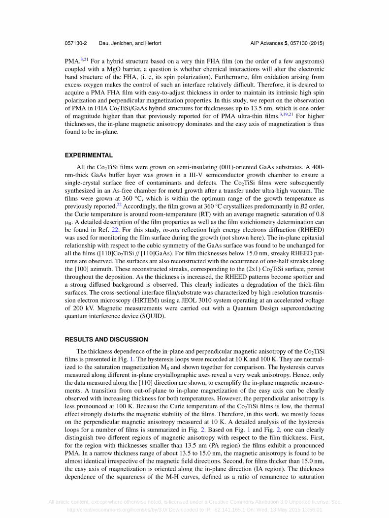
The thickness dependence of the in-plane and perpendicular magnetic anisotropy of the Co2TiSifilms is presented in Fig. 1. The hysteresis loops were recorded at 10 K and 100 K. They are normal-ized to the saturation magnetization MS and shown together for comparison. The hysteresis curvesmeasured along different in-plane crystallographic axes reveal a very weak anisotropy. Hence, onlythe data measured along the [110] direction are shown, to exemplify the in-plane magnetic measure-ments. A transition from out-of-plane to in-plane magnetization of the easy axis can be clearlyobserved with increasing thickness for both temperatures. However, the perpendicular anisotropy isless pronounced at 100 K. Because the Curie temperature of the Co2TiSi films is low, the thermaleffect strongly disturbs the magnetic stability of the films. Therefore, in this work, we mostly focuson the perpendicular magnetic anisotropy measured at 10 K. A detailed analysis of the hysteresisloops for a number of films is summarized in Fig. 2. Based on Fig. 1 and Fig. 2, one can clearlydistinguish two different regions of magnetic anisotropy with respect to the film thickness. First,for the region with thicknesses smaller than 13.5 nm (PA region) the films exhibit a pronouncedPMA. In a narrow thickness range of about 13.5 to 15.0 nm, the magnetic anisotropy is found to bealmost identical irrespective of the magnetic field directions. Second, for films thicker than 15.0 nm,the easy axis of magnetization is oriented along the in-plane direction (IA region). The thicknessdependence of the squareness of the M-H curves, defined as a ratio of remanence to saturation
All article content, except where otherwise noted, is licensed under a Creative Commons Attribution 3.0 Unported license. See:
http://creativecommons.org/licenses/by/3.0/ Downloaded to IP: 62.141.165.1 On: Wed, 13 May 2015 13:56:01
057130-3 Dau, Jenichen, and Herfort AIP Advances 5, 057130 (2015)
FIG. 1. M-H loops of the Co2TiSi films with different thicknesses taken at 10 K and 100 K along directions perpendicular[001] and parallel [110] to the sample surface. The diamagnetic contribution of the GaAs substrate was subtracted.
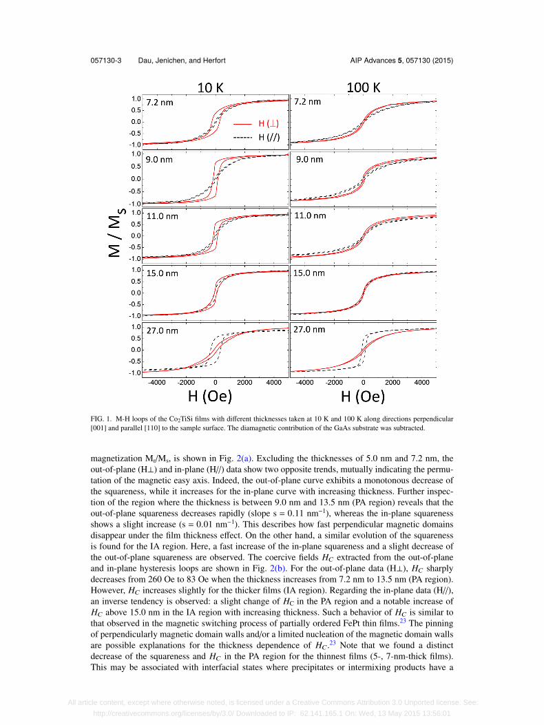
magnetization Mr/Ms, is shown in Fig. 2(a). Excluding the thicknesses of 5.0 nm and 7.2 nm, theout-of-plane (H⊥) and in-plane (H//) data show two opposite trends, mutually indicating the permu-tation of the magnetic easy axis. Indeed, the out-of-plane curve exhibits a monotonous decrease ofthe squareness, while it increases for the in-plane curve with increasing thickness. Further inspec-tion of the region where the thickness is between 9.0 nm and 13.5 nm (PA region) reveals that theout-of-plane squareness decreases rapidly (slope s = 0.11 nm−1), whereas the in-plane squarenessshows a slight increase (s = 0.01 nm−1). This describes how fast perpendicular magnetic domainsdisappear under the film thickness effect. On the other hand, a similar evolution of the squarenessis found for the IA region. Here, a fast increase of the in-plane squareness and a slight decrease ofthe out-of-plane squareness are observed. The coercive fields HC extracted from the out-of-planeand in-plane hysteresis loops are shown in Fig. 2(b). For the out-of-plane data (H⊥), HC sharplydecreases from 260 Oe to 83 Oe when the thickness increases from 7.2 nm to 13.5 nm (PA region).However, HC increases slightly for the thicker films (IA region). Regarding the in-plane data (H//),an inverse tendency is observed: a slight change of HC in the PA region and a notable increase ofHC above 15.0 nm in the IA region with increasing thickness. Such a behavior of HC is similar tothat observed in the magnetic switching process of partially ordered FePt thin films.23 The pinningof perpendicularly magnetic domain walls and/or a limited nucleation of the magnetic domain wallsare possible explanations for the thickness dependence of HC.23 Note that we found a distinctdecrease of the squareness and HC in the PA region for the thinnest films (5-, 7-nm-thick films).This may be associated with interfacial states where precipitates or intermixing products have a
All article content, except where otherwise noted, is licensed under a Creative Commons Attribution 3.0 Unported license. See:
http://creativecommons.org/licenses/by/3.0/ Downloaded to IP: 62.141.165.1 On: Wed, 13 May 2015 13:56:01
057130-4 Dau, Jenichen, and Herfort AIP Advances 5, 057130 (2015)
FIG. 2. (a) Squareness Mr/Ms, (b) Hc and (c) Saturation magnetization Ms obtained from the in-plane and out-of-planehysteresis loops at 10 K and plotted as a function of the film thickness. PA and IA regions correspond to PMA films andin-plane magnetic anisotropy films, respectively. The solid line in figure (c) is to guide the eyes.
significant contribution to the magnetic properties. The interfacial state, which will be discussed inthe following section, may also affect the saturation magnetizations of the thinnest films (Fig. 2(c))since they are remarkably low and anisotropic for the in-plane and out-of-plane measurements.However, the interfacial contribution to the saturation magnetization becomes negligible when thethickness is above 15.0 nm.
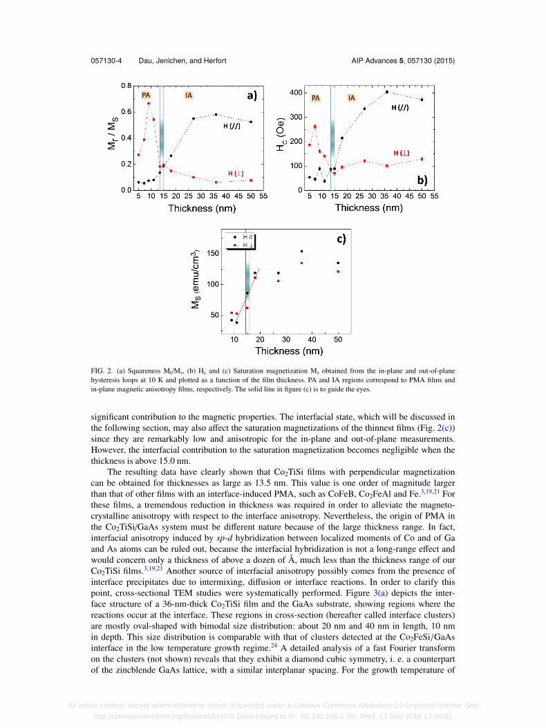
The resulting data have clearly shown that Co2TiSi films with perpendicular magnetizationcan be obtained for thicknesses as large as 13.5 nm. This value is one order of magnitude largerthan that of other films with an interface-induced PMA, such as CoFeB, Co2FeAl and Fe.3,19,21 Forthese films, a tremendous reduction in thickness was required in order to alleviate the magneto-crystalline anisotropy with respect to the interface anisotropy. Nevertheless, the origin of PMA inthe Co2TiSi/GaAs system must be different nature because of the large thickness range. In fact,interfacial anisotropy induced by sp-d hybridization between localized moments of Co and of Gaand As atoms can be ruled out, because the interfacial hybridization is not a long-range effect andwould concern only a thickness of above a dozen of Å, much less than the thickness range of ourCo2TiSi films.3,19,21 Another source of interfacial anisotropy possibly comes from the presence ofinterface precipitates due to intermixing, diffusion or interface reactions. In order to clarify thispoint, cross-sectional TEM studies were systematically performed. Figure 3(a) depicts the inter-face structure of a 36-nm-thick Co2TiSi film and the GaAs substrate, showing regions where thereactions occur at the interface. These regions in cross-section (hereafter called interface clusters)are mostly oval-shaped with bimodal size distribution: about 20 nm and 40 nm in length, 10 nmin depth. This size distribution is comparable with that of clusters detected at the Co2FeSi/GaAsinterface in the low temperature growth regime.24 A detailed analysis of a fast Fourier transformon the clusters (not shown) reveals that they exhibit a diamond cubic symmetry, i. e. a counterpartof the zincblende GaAs lattice, with a similar interplanar spacing. For the growth temperature of
All article content, except where otherwise noted, is licensed under a Creative Commons Attribution 3.0 Unported license. See:
http://creativecommons.org/licenses/by/3.0/ Downloaded to IP: 62.141.165.1 On: Wed, 13 May 2015 13:56:01
057130-5 Dau, Jenichen, and Herfort AIP Advances 5, 057130 (2015)
FIG. 3. (a) Cross-sectional TEM micrographs of the interface Co2TiSi/GaAs with a typical interfacial cluster (indicated bythe arrow). The scale bars correspond to 5 nm. (b) SAED of the Co2TiSi film taken with the zone axis [110]. (c) Kineticsimulation of diffraction peaks of the Co2TiSi lattice obtained with the zone axis [110].
360 ◦C, it is known that metallic elements from the Co2TiSi films may chemically react with theGaAs substrates giving rise to interfacial products. Co-based or Ti-based phases such as Co2GaAs,CoAs, TiAs, Ti1−xGax might be formed in this condition.24,26 However, these have either an ortho-rhombic or hexagonal structure with a different lattice constant from that of GaAs.25,26 We note thatthe x-ray diffraction scans did not show any additional peaks besides those of Co2TiSi and GaAs.Therefore, these findings strongly suggest that interface clusters originate from the in-diffusion ofthe Co2TiSi film into the substrate rather than from chemical reactions. An inspection by electronenergy loss spectroscopy (EELS) (not shown) also evidenced the incorporation of Co and Ti in theseclusters, resulting in dilute Co and Ti clusters. The selected area electron diffraction (SAED) patternof the film in the vicinity of the interface area, and the simulated pattern, are shown in the Fig.3(b) and 3(c), respectively. The diffraction peaks of the SAED pattern are identical to those of thesimulated pattern, confirming the typical cubic lattice of Co2TiSi with long-range crystallinity andorder. Apart from the clusters and the film quality in the interface area, we observe polycrystallineand amorphous regions which are mostly located in the upper part of the film (about 20 nm from theinterface). This is actually consistent with the degradation of the RHEED patterns with increasingfilm thickness. We emphasize that the interesting information obtained from the TEM investigationis the presence of clusters at the interface which can be apparently expected for the whole range ofthickness studied.
An obvious question is how the clusters affect the magnetic properties of the films. Indeed,these clusters, which contain magnetic Co ions, may be considered as diluted magnetic clusters.27
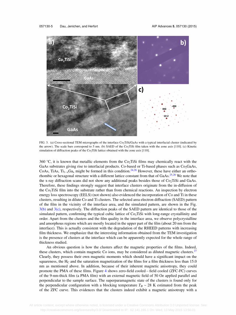
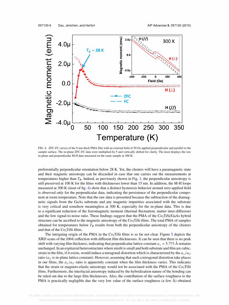
Clearly, they possess their own magnetic moments which should have a significant impact on thesquareness, the HC and the saturation magnetization of the films for a film thickness less than 15.0nm as mentioned above. In addition, because of their inherent magnetic anisotropy, they couldpromote the PMA of these films. Figure 4 shows zero-field cooled – field cooled (ZFC-FC) curvesof the 9-nm-thick film (a PMA film) with an external magnetic field of 50 Oe applied parallel andperpendicular to the sample surface. The superparamagnetic state of the clusters is found only forthe perpendicular configuration with a blocking temperature TB ∼ 28 K estimated from the peakof the ZFC curve. This evidences that the clusters indeed exhibit a magnetic anisotropy with a
All article content, except where otherwise noted, is licensed under a Creative Commons Attribution 3.0 Unported license. See:
http://creativecommons.org/licenses/by/3.0/ Downloaded to IP: 62.141.165.1 On: Wed, 13 May 2015 13:56:01
057130-6 Dau, Jenichen, and Herfort AIP Advances 5, 057130 (2015)
FIG. 4. ZFC-FC curves of the 9-nm-thick PMA film with an external field of 50 Oe applied perpendicular and parallel to thesample surface. The in-plane ZFC-FC data were multiplied by 5 and vertically shifted for clarity. The inset displays the rawin-plane and perpendicular M-H data measured on the same sample at 300 K.
preferentially perpendicular orientation below 28 K. Yet, the clusters will have a paramagnetic stateand their magnetic anisotropy can be discarded in case that one carries out the measurements attemperatures higher than TB. Indeed, as previously shown in Fig. 1, the perpendicular anisotropy isstill preserved at 100 K for the films with thicknesses lower than 15 nm. In addition, the M-H loopsmeasured at 300 K (inset of fig. 4) show that a distinct hysteresis behavior around zero-applied fieldis observed only for the perpendicular data, indicating the persistence of the perpendicular compo-nent at room temperature. Note that the raw data is presented because the subtraction of the diamag-netic signals from the GaAs substrate and any magnetic impurities associated with the substrateis very critical and somehow meaningless at 300 K, especially for the in-plane data. This is dueto a significant reduction of the ferromagnetic moment (thermal fluctuation, matter inter-diffusion)and the low signal-to-noise ratio. These findings suggest that the PMA of the Co2TiSi/GaAs hybridstructure can be ascribed to the magnetic anisotropy of the Co2TiSi films. The total PMA of samplesobtained for temperatures below TB results from both the perpendicular anisotropy of the clustersand that of the Co2TiSi films.
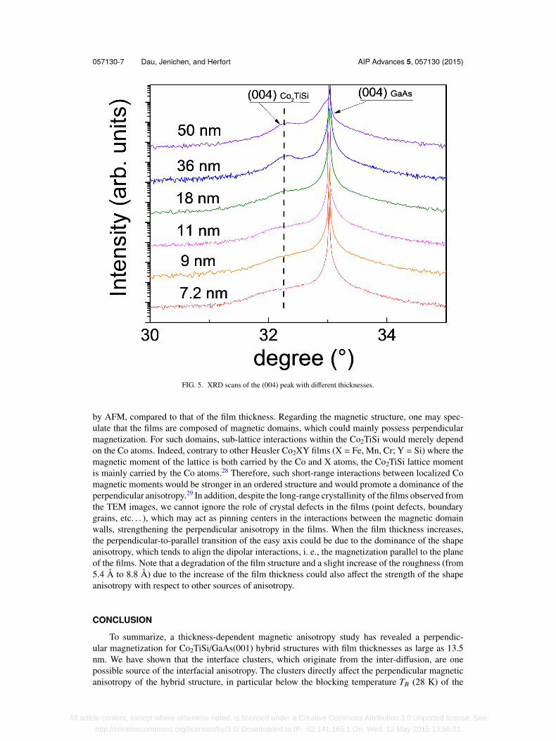
The intriguing origin of the PMA in the Co2TiSi films is so far not clear. Figure 5 depicts theXRD scans of the (004) reflection with different film thicknesses. It can be seen that there is no peakshift with varying film thickness, indicating that perpendicular lattice constant a⊥ = 5.773 Å remainsunchanged. In an expitaxial heterostructure where misfit is small and both substrate and film are cubic,strain in the film, if it exists, would induce a tetragonal distortion which is characterized by the a⊥/a//
ratio (a// is in-plane lattice constant). However, assuming that such a tetragonal distortion take placesin our films, the a⊥/a// ratio is apparently constant when the film thickness varies. This indicatesthat the strain or magneto-elastic anisotropy would not be associated with the PMA of the Co2TiSifilms. Furthermore, the interfacial anisotropy induced by the hybridization nature of the bonding canbe ruled out due to the large film thicknesses. Also, the contribution of the surface roughness to thePMA is practically negligible due the very low value of the surface roughness (a few Å) obtained
All article content, except where otherwise noted, is licensed under a Creative Commons Attribution 3.0 Unported license. See:
http://creativecommons.org/licenses/by/3.0/ Downloaded to IP: 62.141.165.1 On: Wed, 13 May 2015 13:56:01
057130-7 Dau, Jenichen, and Herfort AIP Advances 5, 057130 (2015)
FIG. 5. XRD scans of the (004) peak with different thicknesses.
by AFM, compared to that of the film thickness. Regarding the magnetic structure, one may spec-ulate that the films are composed of magnetic domains, which could mainly possess perpendicularmagnetization. For such domains, sub-lattice interactions within the Co2TiSi would merely dependon the Co atoms. Indeed, contrary to other Heusler Co2XY films (X = Fe, Mn, Cr; Y = Si) where themagnetic moment of the lattice is both carried by the Co and X atoms, the Co2TiSi lattice momentis mainly carried by the Co atoms.28 Therefore, such short-range interactions between localized Comagnetic moments would be stronger in an ordered structure and would promote a dominance of theperpendicular anisotropy.29 In addition, despite the long-range crystallinity of the films observed fromthe TEM images, we cannot ignore the role of crystal defects in the films (point defects, boundarygrains, etc. . . ), which may act as pinning centers in the interactions between the magnetic domainwalls, strengthening the perpendicular anisotropy in the films. When the film thickness increases,the perpendicular-to-parallel transition of the easy axis could be due to the dominance of the shapeanisotropy, which tends to align the dipolar interactions, i. e., the magnetization parallel to the planeof the films. Note that a degradation of the film structure and a slight increase of the roughness (from5.4 Å to 8.8 Å) due to the increase of the film thickness could also affect the strength of the shapeanisotropy with respect to other sources of anisotropy.
CONCLUSION
To summarize, a thickness-dependent magnetic anisotropy study has revealed a perpendic-ular magnetization for Co2TiSi/GaAs(001) hybrid structures with film thicknesses as large as 13.5nm. We have shown that the interface clusters, which originate from the inter-diffusion, are onepossible source of the interfacial anisotropy. The clusters directly affect the perpendicular magneticanisotropy of the hybrid structure, in particular below the blocking temperature TB (28 K) of the
All article content, except where otherwise noted, is licensed under a Creative Commons Attribution 3.0 Unported license. See:
http://creativecommons.org/licenses/by/3.0/ Downloaded to IP: 62.141.165.1 On: Wed, 13 May 2015 13:56:01
057130-8 Dau, Jenichen, and Herfort AIP Advances 5, 057130 (2015)
clusters. However, as the perpendicular component persists up to room temperature, well above TB,the anisotropy contribution from the clusters can be separated and we can attribute the perpendic-ular anisotropy to the magnetic properties of the Co2TiSi films. These results open up promisingperspectives of the Co2TiSi/GaAs hybrid structures not only for spin transport in semiconductordevices at remanence, but also for oxide-based magnetic tunnel junctions with perpendicularlymagnetized electrodes.
ACKNOWLEDGEMENTS
The authors would like to thank Claudia Hermann for MBE assistance, Doreen Steffen forsample preparation and Xiang Kong for EELS measurements. The authors gratefully acknowledgethe critical reading of Yukihiko Takagaki. This work was supported by the German DFG within thepriority program SPP 1538.1 M. Albrecht, C. T. Rettner, A. Moser, M. E. Best, and B. D. Terris, Appl. Phys. Lett. 81, 2875 (2002).2 A. D. Kent, B. Özyilmaz, and E. Del Barco, Appl. Phys. Lett. 84, 3897 (2004).3 S. Ikeda, K. Miura, H. Yamamoto, K. Mizunuma, H. D. Gan, M. Endo, S. Kanai, J. Hayakawa, F. Matsukura, and H. Ohno,
Nat. Mat. 9, 721 (2010).4 M. Ramsteiner, O. Brandt, T. Flissikowski, H. T. Grahn, M. Hashimoto, J. Herfort, and H. Kostial, Phys. Rev. B 78, 121303
(2008).5 R. Farshchi, M. Ramsteiner, J. Herfort, A. Tahraoui, and H. T. Grahn, Appl. Phys. Lett. 98, 162508 (2011).6 S. Jeong, Y.-N. Hsu, D. E. Laughlin, and M. E. McHenry, IEEE Trans. Magn. 36, 2336 (2000).7 T. Shima, K. Takanashi, Y. K. Takahashi, and K. Hono, Appl. Phys. Lett. 85, 2571 (2004).8 H. Van Kranenburg, J. C. Udder, Y. Maeda, L. Toth, and Th. J. A. Popma, IEEE Trans. Magn. 26, 1620 (1990).9 V. G. Harris and T. Pokhil, Phys. Rev. Lett. 87, 067207 (2001).
10 F. Richomme, J. Teillet, A. Fnidiki, and W. Keune, Phys. Rev. B 64, 094415 (2001).11 M. Gottwald, K. Lee, J. J. Kan, B. Ocker, J. Wrona, S. Tibus, J. Langer, S. H. Kang, and E. E. Fullerton, Appl. Phys. Lett.
102, 052405 (2013).12 M. T. Johnson, P. J. H. Bloemen, F. J. A. den Broeder, and J. J. de Vries, Rep. Prog. Phys. 59, 1409 (1996).13 N. Nakajima, T. Koide, T. Shidara, H. Miyauchi, H. Fukutani, A. Fujimori, K. Iio, and T. Katayama, Phys. Rev. Lett. 81,
5229 (1998).14 S. J. Hashemifar, P. Kratzer, and M. Scheffler, Phys. Rev. Lett. 94, 096402 (2005).15 V. Koa, G. Hana, and Y.P. Feng, J. Magn. Magn. Mater. 322, 2989 (2010).16 T. Ambrose, J. J. Krebs, and G. A. Prinz, Appl. Phys. Lett. 76, 3280 (2000).17 M. Hashimoto, J. Herfort, H.-P. Schonherr, and K. H. Ploog, Appl. Phys. Lett. 87, 102506 (2005).18 M. Belmeguenai, F. Zighem, D. Faurie, H. Tuzcuoglu, S.-M. Chérif, P. Moch, K. Westerholt, and W. Seiler, Phys. Status
Solidi A 209, 1328 (2012).19 Z. Wen, H. Sukegawa, S. Mitani, and K. Inomata, Appl. Phys. Lett. 98, 242507 (2011).20 Y. Cui, B. Khodadadi, S. Schäfer, T. Mewes, J. Lu, and S. A. Wolf, Appl. Phys. Lett. 102, 162403 (2013).21 J. W. Koo, S. Mitani, T. T. Sasaki, H. Sukegawa, Z. C. Wen, T. Ohkubo, T. Niizeki, K. Inomata, and K. Hono, Appl. Phys.
Lett. 103, 192401 (2013).22 M. T. Dau and J. Herfort, J. Phys. D: Appl. Phys. 48, 025003 (2015).23 V. Gehanno, R. Homann, Y. Samson, A. Marty, and S. Auret, Eur. Phys. J. B 10, 457 (1999).24 M. Hashimoto, J. Herfort, A. Trampert, H-P Schönherr, and K. H. Ploog, J. Phys. D: Appl. Phys. 40, 1631 (2007).25 C. J. Palmström, C. C. Chang, A. Yu, G. J. Galvin, and J. W. Mayer, J. Appl. Phys. 62, 3755 (1987).26 K. B. Kim, M. Kniffin, R. Sinclair, and C. R. Helms, J. Vac. Sci. Technol. A 6, 1473 (1988).27 H. Ohno, A. Shen, F. Matsukura, A. Oiwa, A. Endo, S. Katsumoto, and Y. Iye, Appl. Phys. Lett. 69, 363 (1996).28 X. Q. Chen, R. Podloucky, and P. Rogl, J. Appl. Phys. 100, 113901 (2006).29 G. Suran, K. Ounadjela, and F. Machizaud, J. Appl. Phys. 61, 3658 (1987).
All article content, except where otherwise noted, is licensed under a Creative Commons Attribution 3.0 Unported license. See:
http://creativecommons.org/licenses/by/3.0/ Downloaded to IP: 62.141.165.1 On: Wed, 13 May 2015 13:56:01