PCI-Proto Lab/PLX-M · 5 2.2. JTAG Support The PCI bus has connections which may be used for...
28
PCI-Proto Lab/PLX-M Technical Manual HK Meßsysteme GmbH Straße am Heizhaus 1 10318 Berlin / Germany January 2015
Transcript of PCI-Proto Lab/PLX-M · 5 2.2. JTAG Support The PCI bus has connections which may be used for...

PCI-Proto Lab/PLX-M
Technical Manual
HK Meßsysteme GmbH
Straße am Heizhaus 1
10318 Berlin / Germany
January 2015
2
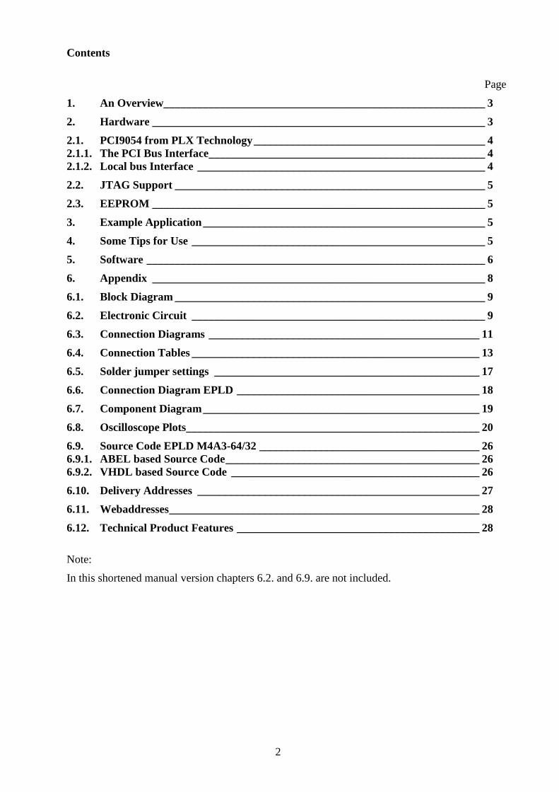
Contents
Page
1. An Overview_________________________________________________________ 3
2. Hardware ___________________________________________________________ 3
2.1. PCI9054 from PLX Technology _________________________________________ 4
2.1.1. The PCI Bus Interface_________________________________________________ 4
2.1.2. Local bus Interface ___________________________________________________ 4
2.2. JTAG Support _______________________________________________________ 5
2.3. EEPROM ___________________________________________________________ 5
3. Example Application __________________________________________________ 5
4. Some Tips for Use ____________________________________________________ 5
5. Software ____________________________________________________________ 6
6. Appendix ___________________________________________________________ 8
6.1. Block Diagram _______________________________________________________ 9
6.2. Electronic Circuit ____________________________________________________ 9
6.3. Connection Diagrams ________________________________________________ 11
6.4. Connection Tables ___________________________________________________ 13
6.5. Solder jumper settings _______________________________________________ 17
6.6. Connection Diagram EPLD ___________________________________________ 18
6.7. Component Diagram _________________________________________________ 19
6.8. Oscilloscope Plots____________________________________________________ 20
6.9. Source Code EPLD M4A3-64/32 _______________________________________ 26
6.9.1. ABEL based Source Code _____________________________________________ 26
6.9.2. VHDL based Source Code ____________________________________________ 26
6.10. Delivery Addresses __________________________________________________ 27
6.11. Webaddresses _______________________________________________________ 28
6.12. Technical Product Features ___________________________________________ 28
Note:
In this shortened manual version chapters 6.2. and 6.9. are not included.

3
1. An Overview
PCI-Proto LAB/PLX-M is an efficient aid for developing add -on boards for personal
computers and other computer systems which are equipped with a PCI bus.
This board makes a quick and uncomplicated test of newly developed electronic circuits on the
PCI bus possible.
PCI-Proto LAB/PLX-M works with the PCI9054 from PLX Technology, Inc., which controls
all typical PCI operation modes and complies with the PCI Local Bus Specification Revision 2.2.
The board is assembled, tested and ready for immediate operation. The system designer can
mount his own hardware directly on the user area and start with the tests. This means that you
can minimize dealing with the signal plays and the technical properties (timing etc.) of the PCI
bus system.
PCI-Proto LAB/PLX-M is a long PCI board manufactured in four layers.
It can be transformed into a short board when cutting it off at the marked place.
PCI-Proto LAB/PLX-M is designed as a universal board that supports either 3.3V or 5V PCI
bus operation.
It's operating voltage for all electronic circuits is 3.3V. PCI-Proto LAB/PLX-M will work at
older PCI slots with 5V if is a Low Drop voltage regulator for 3.3V main supply is mounted at
the board. The user can set /reset (depending on the board) special solder jumpers to archive his
board supply from 5V or 3.3V main supply at the used PCI slot.
The connection for 3.3V and ground is made through each of its own layers. For the 5V supply
there is a grid structure on the component side.
PCI-Proto LAB/PLX-M is delivered with premounted bracket. The user may retro -equip it with
a 15-pin sub-D connector and a BNC connector.
We have added to PCI-Proto LAB/PLX-M's hardware documentation electronic schemes,
component and connection diagrams, EPLD source texts and oscillograms.
2. Hardware
As an introductory description, we will consider the block diagram (Appendix 6.1).
Functionally, the hardware is broken down into three parts:
- PCI controller,
- serial EEPROM,
- Example application with 32 bit latches and EPLD.
4
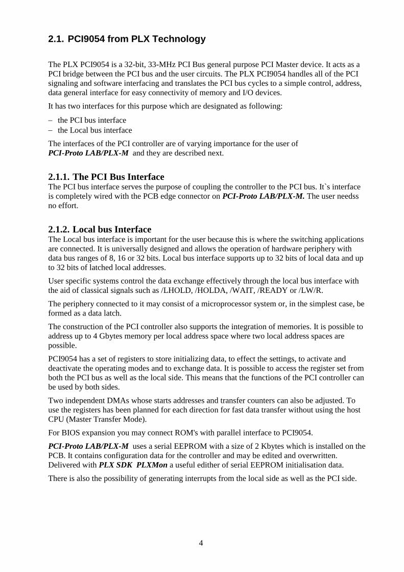
2.1. PCI9054 from PLX Technology
The PLX PCI9054 is a 32-bit, 33-MHz PCI Bus general purpose PCI Master device. It acts as a
PCI bridge between the PCI bus and the user circuits. The PLX PCI9054 handles all of the PCI
signaling and software interfacing and translates the PCI bus cycles to a simple control, address,
data general interface for easy connectivity of memory and I/O devices.
It has two interfaces for this purpose which are designated as following:
the PCI bus interface
the Local bus interface
The interfaces of the PCI controller are of varying importance for the user of
PCI-Proto LAB/PLX-M and they are described next.
2.1.1. The PCI Bus Interface The PCI bus interface serves the purpose of coupling the controller to the PCI bus. It`s interface
is completely wired with the PCB edge connector on PCI-Proto LAB/PLX-M. The user needss
no effort.
2.1.2. Local bus Interface The Local bus interface is important for the user because this is where the switching applications
are connected. It is universally designed and allows the operation of hardware periphery with
data bus ranges of 8, 16 or 32 bits. Local bus interface supports up to 32 bits of local data and up
to 32 bits of latched local addresses.
User specific systems control the data exchange effectively through the local bus interface with
the aid of classical signals such as /LHOLD, /HOLDA, /WAIT, /READY or /LW/R.
The periphery connected to it may consist of a microprocessor system or, in the simplest case, be
formed as a data latch.
The construction of the PCI controller also supports the integration of memories. It is possible to
address up to 4 Gbytes memory per local address space where two local address spaces are
possible.
PCI9054 has a set of registers to store initializing data, to effect the settings, to activate and
deactivate the operating modes and to exchange data. It is possible to access the register set from
both the PCI bus as well as the local side. This means that the functions of the PCI controller can
be used by both sides.
Two independent DMAs whose starts addresses and transfer counters can also be adjusted. To
use the registers has been planned for each direction for fast data transfer without using the host
CPU (Master Transfer Mode).
For BIOS expansion you may connect ROM's with parallel interface to PCI9054.
PCI-Proto LAB/PLX-M uses a serial EEPROM with a size of 2 Kbytes which is installed on the
PCB. It contains configuration data for the controller and may be edited and overwritten.
Delivered with PLX SDK PLXMon a useful edither of serial EEPROM initialisation data.
There is also the possibility of generating interrupts from the local side as well as the PCI side.
5
2.2. JTAG Support
The PCI bus has connections which may be used for `boundary scan` test processes.
PCI-Proto LAB/PLX-M also designated as `JTAG pins`, makes these lines available to the user
on a pin header.
2.3. EEPROM
The serial EEPROM is used in the initializing phase (when booting the host computer). It
contains obligatory configuration data which initialize the PCI controller specifically for the
PCI-Proto LAB/PLX-M application. It is possible to read in, edit and write down the EEPROM
content with the aid of software program PlxMon witch is delivered with PLX SDK.
3. Example Application
PCI-Proto LAB/PLX-M has an example application which has the purpose of showing the user
how various hardware requirements (I/O and memory access, high - and low -active signal plays)
can be adjusted. The application example makes it possible to write and read data long words (32
bit data) without greater hardware expenditures. For this purpose, an simple control signal
decoder has been created which provides control signals for writing and reading data.
PCI-Proto LAB/PLX-M is equipped with latches for intermediate storage of 32 bit data input or
output. The additionally required logic is placed in a EPLDdevice, which also reserves space for
user -specific modifications. It can be programmed 'in system' with a simple connection cable
over the computer parallel port. The source texts for EPLD are a component of this
documentation. Software for EPLD programming is available from your local Lattice sales office
normally without additional costs.
4. Some Tips for Use
In order to successfully design PCI hardware development with PCI-Proto LAB/PLX-M, it is
absolutely necessary to study this documentation and the technical manual on the PCI controller.
If it is not enclosed in the PCI-Proto LAB/PLX-M product, you can request it at no cost from
PLX Technology/USA or Scantec - Topas/Germany. You will find the addresses and telephone
numbers of the companies mentioned in the appendix to this documentation.
You will also find information and tips, how to work with the PCI controller on the Internet. A
technical manual on the PCI9054 is available as a PDF file. It can be downloaded at PLX's web
sides and you will also find some web addresses are also in the appendix

6
The following informations are supposed to help avoid errors and make work with
PCI-Proto LAB/PLX-M easier. We will list them here without putting them any specific order.
PCI-Proto LAB/PLX-M is initialized in such a fashion that there are four I/O and memory
address regions. They make the following accesses possible:
PCI region 0 mem mapped, used for host access to Local/Runtime/DMA registers
PCI region 1 I/O mapped, used for host access to Local/Runtime/DMA registers
PCI region 2 I/O mapped, address range 16 bytes, corresponds with local
address space 0
PCI region 3 mem mapped, address range 16 bytes, corresponds with local
address space 1
The bus range of both local spaces (0 and 1) is initialized to 32 bit. It is possible to access the
latches installed as an example application with 32 bit, 16 bit and 8 bit read- or write
commands. You can access to the latches with I/O (use base address of PCI-Region 2) or
memory based commands (use base address of PCI region 3).
If you read and write 32 bit data use the address offset 0 only, if you read and write 16 bit data
use the address offsets 0 or 2 and if you read and write 8 bit data you might use the address
offsets 0, 1, 2 or 3.
PCI-Proto LAB/PLX-M has its own vendor ID , device ID, Sub vendor ID and Sub system
ID. The vendor ID (10B5h) and device ID (9054h) is given by the PCI-SIG to PLX
Technology and should not be changed. The sub device ID (9054h) was issued from PLX
Technology for the used type of PCI controller and should also not be changed. The sub
system ID (2263h) was issued specifically for the product PCI-Proto LAB/PLX-M. The user
may apply for his own device ID from PLX Technology for his application. Ask your local
PLX dealer for futher informations.
5. Software
Matching Product Software is optionally available with PCI-Proto LAB/PLX-M.
PLX SDK (original manufacturer: PLX Technology), includes Host API Libraries (Application
Programming Interface) for the PCI controller, WindowsXP /2000 /NT /98/Linux drivers and
some source codes examples.
PLX SDK version comes with a useful monitor program PlxMon. This program makes it
possible to read and write data in BYTE, LWORD and DWORD formats over I/O or memory
accesses. The on board installed Example Application hardware is accessible with the PlxMon
program too. PlxMon makes it easy to change PCI controller configurations and initialisations,
allows the user to read and write the contents of the serial configuration EEPROM and much
more.

7
There are two different variations to get access to the data latches:
- I/O commands (use PCI address region 2, corresponds with local address space 0) or
- Memory commands (use PCI address region 3, corresponds with local address space 1).
The following address offsets are defined for the Example Application:
for 32bit data access:
offset 0h data bits 0 -31, lane 0, 1, 2, 3
for 16bit data access:
offset 0h data bits 0 -15, lane 0, 1
offset 2h data bits 15 -31, lane 2, 3
for 8bit data access:
offset 0h data bits 0 -7, lane 0
offset 1h data bits 8 -15, lane 1
offset 2h data bits 16 -23, lane 2
offset 3h data bits 24 -31, lane 3
The user finds further information about handling and use of the PLX SDK and the
accompanying software on the disk containing manuals and documentation.
The PLX SDK software package is not accompanying part of the PCI-Proto LAB/PLX-M
product.
The PLX SDK software come from firma PLX Technology as a free - download from this WEB
presentation.

8
6. Appendix

9
6.1. Block Diagram
6.2. Electronic Circuit
In this shortened manual version this chapter is not included.

10
11
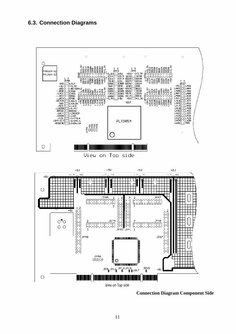
6.3. Connection Diagrams
Connection Diagram Component Side
12
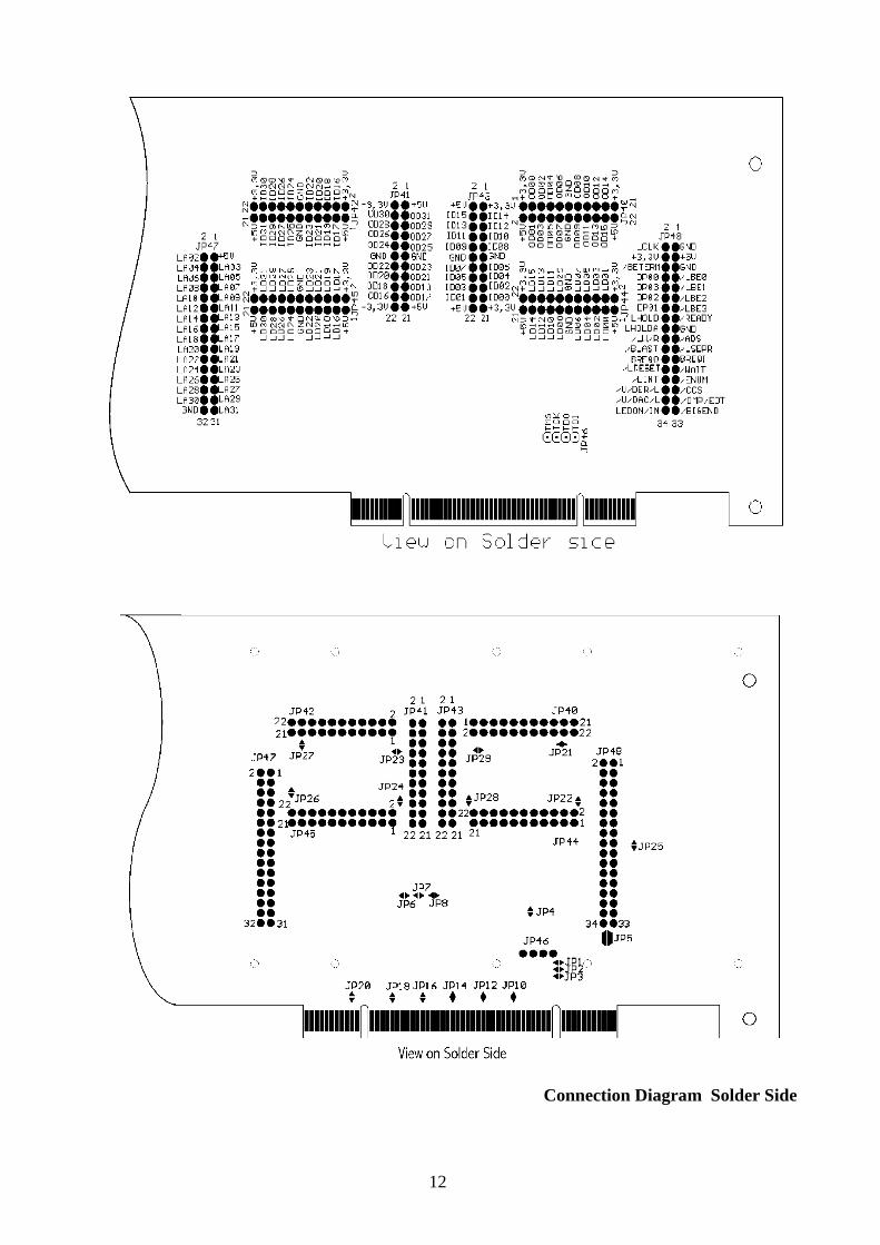
Connection Diagram Solder Side

13
6.4. Connection Tables
Connection Table Pin Header J40, J41
Pin Name Pin Name
01 +3,3V 02 +5V
03 out_data 00 04 out_data 01
05 out_data 02 06 out_data 03
07 out_data 04 08 out_data 05
09 out_data 06 10 out_data 07
11 GND 12 GND
13 out_data 08 14 out_data 09
15 out_data 10 16 out_data 11
17 out_data 12 18 out_data 13
19 out_data 14 20 out_data 15
21 +3,3V 22 +5V
Connection Table Pin Header J40 (User bus/ data output 0 - 15)
Pin Name Pin Name
01 +5V 02 +3,3V
03 out_data 31 04 out_data 30
05 out_data 29 06 out_data 28
07 out_data 27 08 out_data 26
09 out_data 25 10 out_data 24
11 GND 12 GND
13 out_data 23 14 out_data 22
15 out_data 21 16 out_data 20
17 out_data 19 18 out_data 18
19 out_data 17 20 out_data 16
21 +5V 22 +3,3V
Connection Table Pin Header J41 (User bus/ data output 16 - 31)

14
Connection Table Pin Header J42, J43
Pin Name Pin Name
01 +5V 02 +3,3V
03 in_data 17 04 in_data 16
05 in_data 19 06 in_data 18
07 in_data 21 08 in_data 20
09 in_data 23 10 in_data 22
11 GND 12 GND
13 in_data 25 14 in_data 24
15 in_data 27 16 in_data 26
17 in_data 29 18 in_data 28
19 in_data 31 20 in_data 30
21 +5V 22 +3,3V
Connection Table Pin Header J42 (User bus/ data input 16 - 31)
Pin Name Pin Name
01 +3,3V 02 +5V
03 in_data 14 04 in_data 15
05 in_data 12 06 in_data 13
07 in_data 10 08 in_data 11
09 in_data 08 10 in_data 09
11 GND 12 GND
13 in_data 06 14 in_data 07
15 in_data 04 16 in_data 05
17 in_data 02 18 in_data 03
19 in_data 00 20 in_data 01
21 +3,3V 22 +5V
Connection Table Pin Header J43 (User bus/ data input 0 - 15)
15
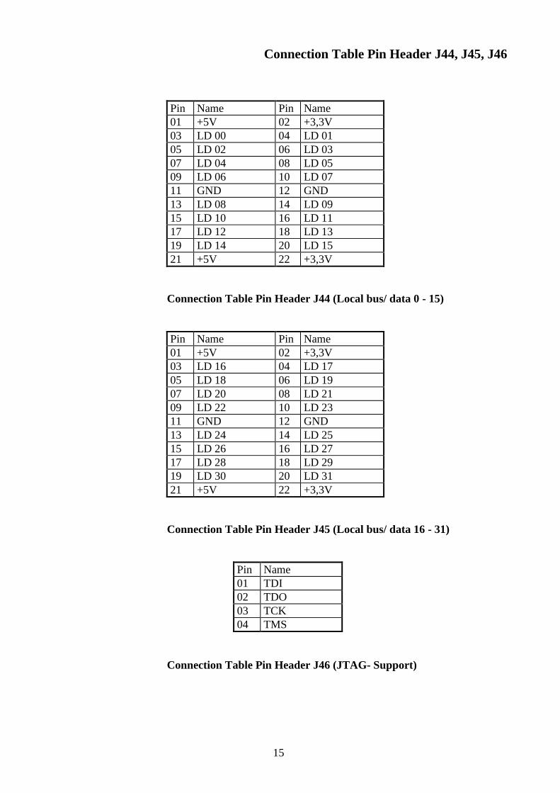
Connection Table Pin Header J44, J45, J46
Pin Name Pin Name
01 +5V 02 +3,3V
03 LD 00 04 LD 01
05 LD 02 06 LD 03
07 LD 04 08 LD 05
09 LD 06 10 LD 07
11 GND 12 GND
13 LD 08 14 LD 09
15 LD 10 16 LD 11
17 LD 12 18 LD 13
19 LD 14 20 LD 15
21 +5V 22 +3,3V
Connection Table Pin Header J44 (Local bus/ data 0 - 15)
Pin Name Pin Name
01 +5V 02 +3,3V
03 LD 16 04 LD 17
05 LD 18 06 LD 19
07 LD 20 08 LD 21
09 LD 22 10 LD 23
11 GND 12 GND
13 LD 24 14 LD 25
15 LD 26 16 LD 27
17 LD 28 18 LD 29
19 LD 30 20 LD 31
21 +5V 22 +3,3V
Connection Table Pin Header J45 (Local bus/ data 16 - 31)
Pin Name
01 TDI
02 TDO
03 TCK
04 TMS
Connection Table Pin Header J46 (JTAG- Support)
16
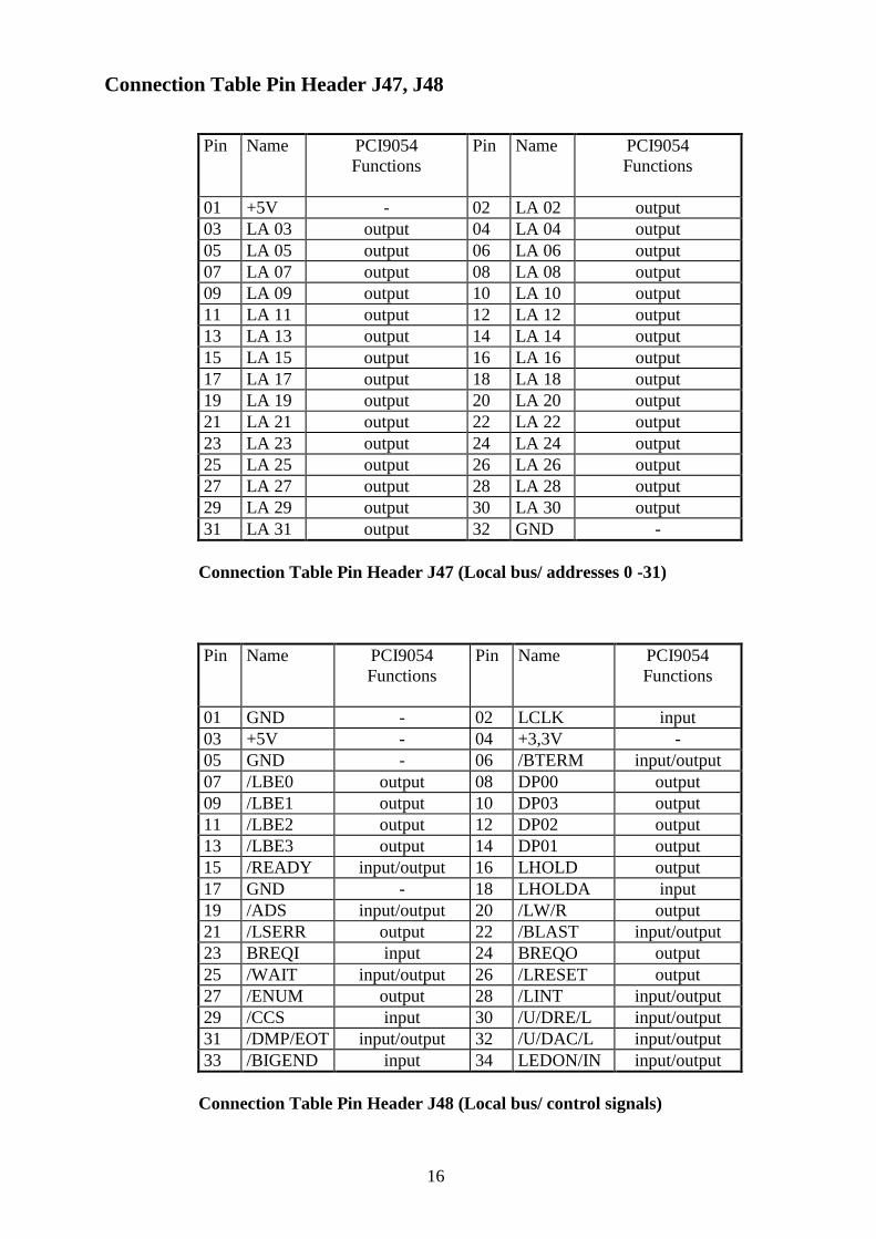
Connection Table Pin Header J47, J48
Pin Name PCI9054
Functions
Pin Name PCI9054
Functions
01 +5V - 02 LA 02 output
03 LA 03 output 04 LA 04 output
05 LA 05 output 06 LA 06 output
07 LA 07 output 08 LA 08 output
09 LA 09 output 10 LA 10 output
11 LA 11 output 12 LA 12 output
13 LA 13 output 14 LA 14 output
15 LA 15 output 16 LA 16 output
17 LA 17 output 18 LA 18 output
19 LA 19 output 20 LA 20 output
21 LA 21 output 22 LA 22 output
23 LA 23 output 24 LA 24 output
25 LA 25 output 26 LA 26 output
27 LA 27 output 28 LA 28 output
29 LA 29 output 30 LA 30 output
31 LA 31 output 32 GND -
Connection Table Pin Header J47 (Local bus/ addresses 0 -31)
Pin Name PCI9054
Functions
Pin Name PCI9054
Functions
01 GND - 02 LCLK input
03 +5V - 04 +3,3V -
05 GND - 06 /BTERM input/output
07 /LBE0 output 08 DP00 output
09 /LBE1 output 10 DP03 output
11 /LBE2 output 12 DP02 output
13 /LBE3 output 14 DP01 output
15 /READY input/output 16 LHOLD output
17 GND - 18 LHOLDA input
19 /ADS input/output 20 /LW/R output
21 /LSERR output 22 /BLAST input/output
23 BREQI input 24 BREQO output
25 /WAIT input/output 26 /LRESET output
27 /ENUM output 28 /LINT input/output
29 /CCS input 30 /U/DRE/L input/output
31 /DMP/EOT input/output 32 /U/DAC/L input/output
33 /BIGEND input 34 LEDON/IN input/output
Connection Table Pin Header J48 (Local bus/ control signals)

17
6.5. Solder jumper settings
Jumper default
setting
Function
open closed
1 closed motherboard JTAG chain broken Motherboard JTAG chain closed
2 closed Card Power Requirement Indication
PRSNT1# is open (high)
Card Power Requirement Indication
PRSNT1# is low
3 open Card Power Requirement Indication
PRSNT2# is open (high)
Card Power Requirement Indication
PRSNT2# is low
4 open blank or programmed serial
EEPROM present on board 1)
no serial EEPROM
present on board 1)
5 closed +3.3V Main Supply active 2)
+5V Main Supply active 2)
6 open TEST input pin (PCI9054) is low TEST input pin (PCI9054) is high
7 open MODE0 input pin (PCI9054) is low MODE0 input pin (PCI9054) is high
8 open MODE1 input pin (PCI9054) is low MODE1 input pin (PCI9054) is high
9 open +5V Main Supply active 2)
+3.3V Main Supply active 2)
10 open +5V Main Supply active 2)
+3.3V Main Supply active 2)
11 open +5V Main Supply active 2)
+3.3V Main Supply active 2)
12 open +5V Main Supply active 2)
+3.3V Main Supply active 2)
13 open +5V Main Supply active 2)
+3.3V Main Supply active 2)
14 open +5V Main Supply active 2)
+3.3V Main Supply active 2)
15 open +5V Main Supply active 2)
+3.3V Main Supply active 2)
16 open +5V Main Supply active 2)
+3.3V Main Supply active 2)
17 open +5V Main Supply active 2)
+3.3V Main Supply active 2)
18 open +5V Main Supply active 2)
+3.3V Main Supply active 2)
19 open +5V Main Supply active 2)
+3.3V Main Supply active 2)
20 open +5V Main Supply active 2)
+3.3V Main Supply active 2)
21 closed Output latch 'Data 8- 15' at tristate Output latch 'Data 8- 15' active 3)
22 closed Output latch 'Data 0- 7' at tristate Output latch 'Data 0- 7' active 3)
23 closed Output latch 'Data 24- 31' at tristate Output latch 'Data 24- 31' active 3)
24 closed Output latch 'Data 16- 23' at tristate Output latch 'Data 16- 23' active 3)
25 open /LHOLD and /LHOLDA are
disconnected
/LHOLD and /LHOLDA are
connected
26 closed Input latch 'Data 16- 23' locked Input latch 'Data 16-23' transparent 3)
27 closed Input latch 'Data 24- 31' locked Input latch 'Data 24-31' transparent 3)
28 closed Input latch 'Data 0- 7' locked Input latch 'Data 0- 7'transparent 3)
29 closed Input latch 'Data 8- 15' locked Input latch 'Data 8- 15'transparent 3)
1) Close J4 for a boot process with absent serial EEPROM ( boot with default values).
2) Close J5 and let J9 - J20 open for +5V main supply, close J9 - J20 and let J5 open for +3.3V main supply.
To prevent electric damages never close J5 and J9-J20 at the same time. Presence of +3.3V supply at the
used slot connector is signalized by Indicator LED D1 (yellow LED).
3) Open J21- 24 and J26- 29 for access to the /OE- and LE- signals from additional electrical circuits.

18
6.6. Connection Diagram EPLD
Socket Diagram M4A3-64/32 Solder Side
Pin Name M4A3-64/32
Functions
Pin Name M4A3-64/32
Functions
1 GND - 23 GND -
2 LHOLD input 24 OLE2 Output
3 /BTERM input (inactive) 25 BREQI output (inactive)
4 not used I/O 2 26 Not used I/O 18
5 /BLAST output (inactive) 27 /U/DAC/L input (inactive)
6 /LW/R input 28 OLE3 Output
7 LA2 input 29 /LBE3 Input
8 /ADS input (inactive) 30 /U/DRE/L output (inactive)
9 LA3 input 31 /LBE2 Input
10 TDI TDI 32 TDS TDS
11 not used CLK0/I0 33 LCLK CLK1
12 GND - 34 GND -
13 TCLK TCLK 35 TDO TDO
14 /IOE3 output 36 /LBE1 Input
15 /IOE2 output 37 /LBE0 Input
16 /IOE1 output 38 /WAIT output (inactive)
17 /IOE0 output 39 /LRESET Input
18 OLE0 output 40 not used I/O 28
19 not used I/O 13 41 not used I/O 29
20 OLE1 output 42 /READY output
21 BREQO input (inactive) 43 LHOLDA output
22 +3,3V - 44 +3,3V -
19
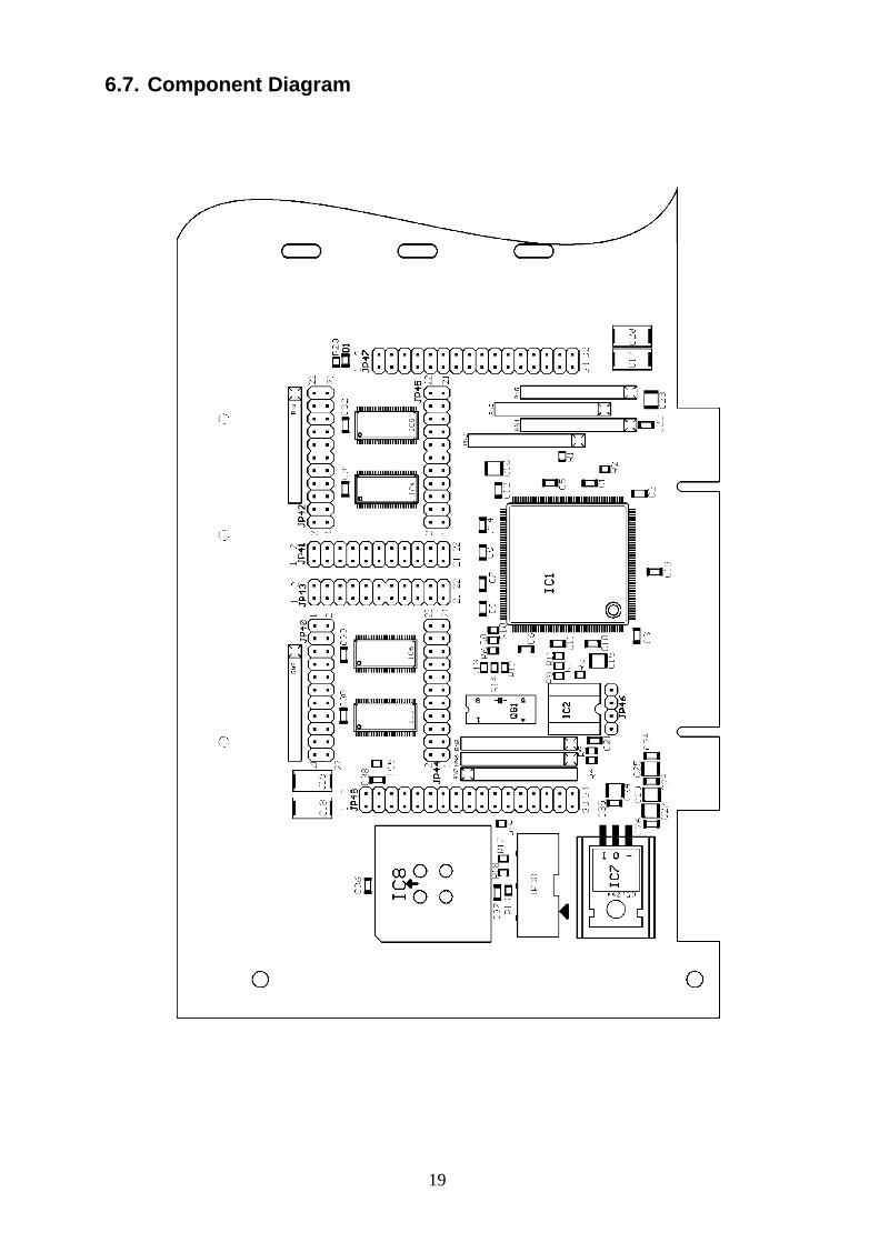
6.7. Component Diagram

20
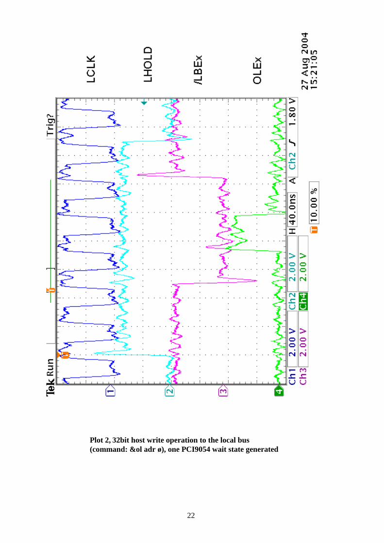
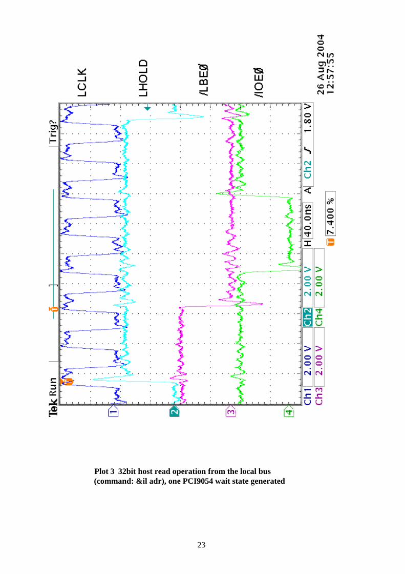
6.8. Oscilloscope Plots

21
Plot 1, host accesses to the example application at the local bus,
one PCI9054 wait state generated
22
Plot 2, 32bit host write operation to the local bus
(command: &ol adr ø), one PCI9054 wait state generated
23
Plot 3 32bit host read operation from the local bus
(command: &il adr), one PCI9054 wait state generated

24
Plot 4, 32bit host write operation to the local bus with
view to a data line LDx (command: &ol adr Ø), one PCI9054 wait
state generated

25
Plot 5, 32bit host read operation from the local bus with view to a data line LDx
(command: &il adr), one PCI9054 wait state generated
26
6.9. Source Code EPLD M4A3-64/32
6.9.1. ABEL based Source Code
6.9.2. VHDL based Source Code
In this shortened manual version this chapters are not included.

27
6.10. Delivery Addresses
Our Hotline:
HK Meßsysteme GmbH Phone: ++49/30/633 75 114
Straße am Heizhaus 1 Fax: ++49/30/633 75 116
D-10318 Berlin/Germany E-Mail: [email protected]
Contact Person: Mathias Kurzweg Web: http://www.pci-tools.com
http://www.pci-tools.de
for our foreign customers in
North America: Japan:
HKM USA Tateno-Dennou Inc.
80 Lancaster Dr. ASO bldg., 5-955 Baigo
Tewksbury, MA 01876 Oume-city, Tokyo, 198-0063 Japan
Fax:++1-978-863-0069 Phone: ++81-428-77-7000
Fax: ++81-428-77-7010
Contact Person: Ilse Seichter Contact Person: Takao Fujii
Email: [email protected] Email: [email protected]
Taiwan Spain
Bentech Computer & Systems Corp. Gerhard Kassner
7F-3, No.23 Lane 169, Kang-Ning Str. Servicios de comunicación
His Chih Chen, Taipei Hsien, Paseo Vergara, 9, 4-4M
Taiwan, R.O.C. 28250 Torrelodones (Madrid)/Spain
Phone: 886-2-2695-8906 Phone/Fax: ++34-91-8590 797
Fax: 886-2-2695-8911 Contact Person: Gerhard Kassner
Contact Person: Benjamin Chu Email: [email protected]
Email: [email protected]
Korea
Dong AH Trade Corporation
371-7 Hwagok 7-Dong,
Kangso-Gu. 157-017,
Seoul, Korea
Phone: 82-2-2065-3311, 82-2-2608-8161
Fax: 82-2-2608-8160
Contact Person: H.J. Lee
Email: [email protected]

28
Manufacturer for PLX PCI9054:
PLX Technology, Inc. Phone: ++1-800-759-3735
390 Potrero Ave. Fax: ++1-408-774-2169
Sunnyvale, CA 94086 Web: http://www.plxtech.com
6.11. Webaddresses
http://www.plxtech.com
http://www.pcisig.com
http://www.pci-tools.de
6.12. Technical Product Features
Features
Bus interface: PCI, in compliance to Local Bus Specification, Revision 2.2
PCI controller: PCI9054, PLX Technology, Inc. (USA)
Size: 12.28 inches x 4.17 inches, (6.85 inches x 4.17 inches after mechanical
cutback)
32 Bit/33 MHz PCI Board, universal card 3.3V/ 5V
Bread board space: 25.1 square inches
Supply: +3.3V, +5V, ±12V, total power requirement class adjustable by solder
Jumpers