PCF8563 Real time clock/calendar - Ethernut · Real time clock/calendar 7.2 Timer The 8-bit...
32
1. General description The PCF8563 is a CMOS real time clock/calendar optimized for low power consumption. A programmable clock output, interrupt output and voltage-low detector are also provided. All address and data are transferred serially via a two-line bidirectional I 2 C-bus. Maximum bus speed is 400 kbit/s. The built-in word address register is incremented automatically after each written or read data byte. 2. Features ■ Provides year, month, day, weekday, hours, minutes and seconds based on 32.768 kHz quartz crystal ■ Century flag ■ Clock operating voltage: 1.8 V to 5.5 V ■ Low backup current; typical 0.25 μA at V DD = 3.0 V and T amb = 25 °C ■ 400 kHz two-wire I 2 C-bus interface (at V DD = 1.8 V to 5.5 V) ■ Programmable clock output for peripheral devices (32.768 kHz, 1024 Hz, 32 Hz and 1 Hz) ■ Alarm and timer functions ■ Integrated oscillator capacitor ■ Internal power-on reset ■ I 2 C-bus slave address: read A3h and write A2h ■ Open-drain interrupt pin ■ ElectroStatic Discharge (ESD) protection exceeds 2000 V Human Body Model (HBM) per JESD22-A114, 200 V Machine Model (MM) per JESD22-A115 and 2 000 V Charged Device Model (CDM) per JESD22-C101 ■ Latch-up testing is done to JEDEC standard JESD78 which exceeds 100 mA 3. Applications ■ Mobile telephones ■ Portable instruments ■ Electronic metering ■ Battery powered products PCF8563 Real time clock/calendar Rev. 05 — 17 July 2007 Product data sheet
Transcript of PCF8563 Real time clock/calendar - Ethernut · Real time clock/calendar 7.2 Timer The 8-bit...
1. General description
The PCF8563 is a CMOS real time clock/calendar optimized for low power consumption.A programmable clock output, interrupt output and voltage-low detector are also provided.All address and data are transferred serially via a two-line bidirectional I2C-bus. Maximumbus speed is 400 kbit/s. The built-in word address register is incremented automaticallyafter each written or read data byte.
2. Features
n Provides year, month, day, weekday, hours, minutes and seconds based on32.768 kHz quartz crystal
n Century flag
n Clock operating voltage: 1.8 V to 5.5 V
n Low backup current; typical 0.25 µA at VDD = 3.0 V and Tamb = 25 °Cn 400 kHz two-wire I2C-bus interface (at VDD = 1.8 V to 5.5 V)
n Programmable clock output for peripheral devices (32.768 kHz, 1024 Hz, 32 Hz and1 Hz)
n Alarm and timer functions
n Integrated oscillator capacitor
n Internal power-on reset
n I2C-bus slave address: read A3h and write A2h
n Open-drain interrupt pin
n ElectroStatic Discharge (ESD) protection exceeds 2000 V Human Body Model (HBM)per JESD22-A114, 200 V Machine Model (MM) per JESD22-A115 and 2000 VCharged Device Model (CDM) per JESD22-C101
n Latch-up testing is done to JEDEC standard JESD78 which exceeds 100 mA
3. Applications
n Mobile telephones
n Portable instruments
n Electronic metering
n Battery powered products
PCF8563Real time clock/calendarRev. 05 — 17 July 2007 Product data sheet
NXP Semiconductors PCF8563Real time clock/calendar
4. Ordering information
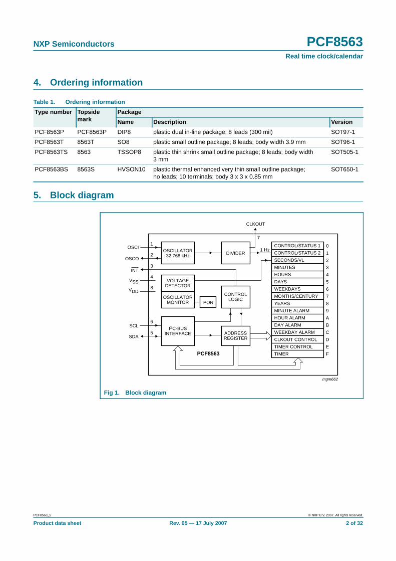
5. Block diagram
Table 1. Ordering information
Type number Topsidemark
Package
Name Description Version
PCF8563P PCF8563P DIP8 plastic dual in-line package; 8 leads (300 mil) SOT97-1
PCF8563T 8563T SO8 plastic small outline package; 8 leads; body width 3.9 mm SOT96-1
PCF8563TS 8563 TSSOP8 plastic thin shrink small outline package; 8 leads; body width3 mm
SOT505-1
PCF8563BS 8563S HVSON10 plastic thermal enhanced very thin small outline package;no leads; 10 terminals; body 3 x 3 x 0.85 mm
SOT650-1
Fig 1. Block diagram
mgm662
0CONTROL/STATUS 1OSCILLATOR
32.768 kHz 1CONTROL/STATUS 2
2SECONDS/VL
3MINUTES
4HOURS
5DAYS
6WEEKDAYS
7MONTHS/CENTURY
8YEARS
9MINUTE ALARM
AHOUR ALARM
BDAY ALARM
CWEEKDAY ALARM
D
E
CLKOUT CONTROL
F
TIMER CONTROL
TIMER
OSCILLATORMONITOR
VOLTAGEDETECTOR
I2C-BUSINTERFACE
DIVIDER
CONTROLLOGIC
ADDRESSREGISTER
POR
PCF8563
VDD
CLKOUT
1 Hz
OSCO
SCL
SDA
VSS
INT
OSCI1
2
3
4
8
6
5
7
PCF8563_5 © NXP B.V. 2007. All rights reserved.
Product data sheet Rev. 05 — 17 July 2007 2 of 32
NXP Semiconductors PCF8563Real time clock/calendar
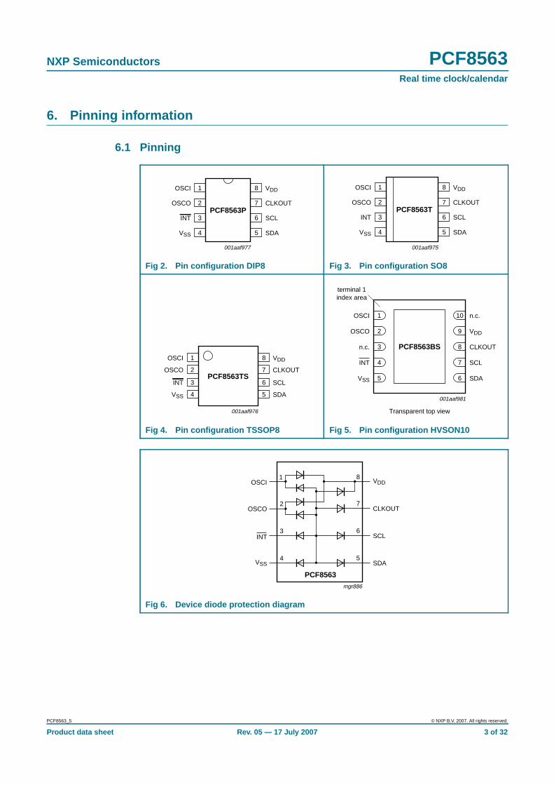
6. Pinning information
6.1 Pinning
Fig 2. Pin configuration DIP8 Fig 3. Pin configuration SO8
Fig 4. Pin configuration TSSOP8 Fig 5. Pin configuration HVSON10
Fig 6. Device diode protection diagram
PCF8563P
OSCI VDD
OSCO CLKOUT
INT SCL
VSS SDA
001aaf977
1
2
3
4
6
5
8
7PCF8563T
OSCI VDD
OSCO CLKOUT
INT SCL
VSS SDA
001aaf975
1
2
3
4
6
5
8
7
PCF8563TS
OSCI VDD
OSCO CLKOUT
INT SCL
VSS SDA
001aaf976
1
2
3
4
6
5
8
7
001aaf981
PCF8563BS
SDA
INT
VSS
SCL
n.c. CLKOUT
OSCO VDD
OSCI n.c.
Transparent top view
5 6
4 7
3 8
2 9
1 10
terminal 1index area
mgr886
SDA4 5
VSS
SCL3 6
INT
CLKOUT2 7
OSCO
VDD1 8
OSCI
PCF8563
PCF8563_5 © NXP B.V. 2007. All rights reserved.
Product data sheet Rev. 05 — 17 July 2007 3 of 32

NXP Semiconductors PCF8563Real time clock/calendar
6.2 Pin description
7. Functional description
The PCF8563 contains sixteen 8-bit registers with an auto-incrementing address register,an on-chip 32.768 kHz oscillator with one integrated capacitor, a frequency divider whichprovides the source clock for the Real Time Clock/calender (RTC), a programmable clockoutput, a timer, an alarm, a voltage-low detector and a 400 kHz I2C-bus interface.
All 16 registers are designed as addressable 8-bit parallel registers although not all bitsare implemented. The first two registers (memory address 00h and 01h) are used ascontrol and/or status registers. The memory addresses 02h through 08h are used ascounters for the clock function (seconds up to years counters). Address locations 09hthrough 0Ch contain alarm registers which define the conditions for an alarm.Address 0Dh controls the CLKOUT output frequency. 0Eh and 0Fh are the timer controland timer registers, respectively.
The seconds, minutes, hours, days, weekdays, months, years as well as the minute alarm,hour alarm, day alarm and weekday alarm registers are all coded in Binary CodedDecimal (BCD) format.
When one of the RTC registers is read the contents of all counters are frozen. Therefore,faulty reading of the clock/calendar during a carry condition is prevented.
7.1 Alarm function modesBy clearing the MSB of one or more of the alarm registers (bit AE = alarm enable), thecorresponding alarm condition(s) will be active. In this way an alarm can be generatedfrom once per minute up to once per week. The alarm condition sets the Alarm Flag (AF).The asserted AF can be used to generate an interrupt (INT). The AF can only be clearedby software.
Table 2. Pin description
Symbol Pin Description
DIP8, SO8,TSSOP8
HVSON10
OSCI 1 1 oscillator input
OSCO 2 2 oscillator output
n.c - 3 not connected
INT 3 4 interrupt output (open-drain; active LOW)
VSS 4 5 ground
SDA 5 6 serial data input and output
SCL 6 7 serial clock input
CLKOUT 7 8 clock output, open-drain
VDD 8 9 positive supply voltage
n.c - 10 not connected
PCF8563_5 © NXP B.V. 2007. All rights reserved.
Product data sheet Rev. 05 — 17 July 2007 4 of 32

NXP Semiconductors PCF8563Real time clock/calendar
7.2 TimerThe 8-bit countdown timer at address 0Fh is controlled by the timer control register ataddress 0Eh. The timer control register determines one of 4 source clock frequencies forthe timer (4096 Hz, 64 Hz, 1 Hz, or 1⁄60 Hz), and enables or disables the timer. The timercounts down from a software-loaded 8-bit binary value. At the end of every countdown,the timer sets the Timer Flag (TF). The TF may only be cleared by software. Theasserted TF can be used to generate an interrupt (INT). The interrupt may be generatedas a pulsed signal every countdown period or as a permanently active signal whichfollows the condition of TF. Bit TI/TP is used to control this mode selection. When readingthe timer, the current countdown value is returned.
7.3 Clock outputA programmable square wave is available at pin CLKOUT. Operation is controlled by theCLKOUT control register at address 0Dh. Frequencies of 32.768 kHz (default), 1024 Hz,32 Hz and 1 Hz can be generated for use as a system clock, microcontroller clock, input toa charge pump, or for calibration of the oscillator. CLKOUT is an open-drain output andenabled at power-on. If disabled it becomes high-impedance.
7.4 ResetThe PCF8563 includes an internal reset circuit which is active whenever the oscillator isstopped. In the reset state the I2C-bus logic is initialized and all registers are resetaccording to Table 25.
7.5 Voltage-low detectorThe PCF8563 has an on-chip voltage-low detector (see Figure 7). When VDD drops belowVlow, bit VL in the seconds register is set to indicate that the integrity of the clockinformation is no longer guaranteed. The VL flag can only be cleared by software.
Bit VL is intended to detect the situation when VDD is decreasing slowly, for example underbattery operation. Should VDD reach Vlow before power is re-asserted then bit VL is set.This will indicate that the time may be corrupted.
Fig 7. Voltage-low detection
VL set
normal poweroperation
period of batteryoperation
t
VDD
Vlow
mgr887
PCF8563_5 © NXP B.V. 2007. All rights reserved.
Product data sheet Rev. 05 — 17 July 2007 5 of 32

NXP Semiconductors PCF8563Real time clock/calendar
7.6 Register organization
7.6.1 Control/status 1 register
7.6.2 Control/status 2 register
Bits TF and AF: When an alarm occurs, AF is set to logic 1. Similarly, at the end of a timercountdown, TF is set to logic 1. These bits maintain their value until overwritten bysoftware. If both timer and alarm interrupts are required in the application, the source ofthe interrupt can be determined by reading these bits. To prevent one flag beingoverwritten while clearing another a logic AND is performed during a write access.
Table 3. Formatted registers overviewBit positions labelled as x are not implemented. Bit positions labelled with 0 should always be written with logic 0; if read theycould be either logic 0 or logic 1.
Address Register name Bit 7 Bit 6 Bit 5 Bit 4 Bit 3 Bit 2 Bit 1 Bit 0
00h control/status 1 TEST1 0 STOP 0 TESTC 0 0 0
01h control/status 2 0 0 0 TI/TP AF TF AIE TIE
02h seconds VL <seconds 00 to 59 coded in BCD>
03h minutes x <minutes 00 to 59 coded in BCD>
04h hours x x <hours 00 to 23 coded in BCD>
05h days x x <days 01 to 31 coded in BCD>
06h weekdays x x x x x <weekdays 0 to 6>
07h months/century C x x <months 01 to 12 coded in BCD>
08h years <years 00 to 99 coded in BCD>
09h minute alarm AE <minute alarm 00 to 59 coded in BCD>
0Ah hour alarm AE x <hour alarm 00 to 23 coded in BCD>
0Bh day alarm AE x <day alarm 01 to 31 coded in BCD>
0Ch weekday alarm AE x x x x <weekday alarm 0 to 6>
0Dh CLKOUT control FE x x x x x FD1 FD0
0Eh timer control AT x x x x x TD1 TD0
0Fh timer <timer countdown value>
Table 4. Control/status 1 (address 00h) bits description
Bit Symbol Value Description
7 TEST1 0 normal mode
1 EXT_CLK test mode
6 0 default value is logic 0
5 STOP 0 RTC source clock runs
1 all RTC divider chain flip-flops are asynchronously set to logic 0;the RTC clock is stopped (CLKOUT at 32.768 kHz is stillavailable)
4 0 default value is logic 0
3 TESTC 0 Power-on reset override facility is disabled; set to logic 0 fornormal operation
1 Power-on reset override may be enabled
2 to 0 0 default value is logic 0
PCF8563_5 © NXP B.V. 2007. All rights reserved.
Product data sheet Rev. 05 — 17 July 2007 6 of 32

NXP Semiconductors PCF8563Real time clock/calendar
Bits TIE and AIE: These bits activate or deactivate the generation of an interrupt whenTF or AF is asserted, respectively. The interrupt is the logical OR of these two conditionswhen both AIE and TIE are set.
[1] TF and INT become active simultaneously.
[2] n = loaded countdown value. Timer stopped when n = 0.
7.6.3 Time and date registers
Table 5. Control/status 2 (address 01h) bits description
Bit Symbol Value Description
7 to 5 0 default value is logic 0
4 TI/TP 0 INT is active when TF is active (subject to the status of TIE)
1 INT pulses active according to Table 6 (subject to the status ofTIE); note that if AF and AIE are active then INT will bepermanently active
3 AF 0 (read) alarm flag inactive
1 (read) alarm flag active
0 (write) alarm flag is cleared
1 (write) alarm flag remains unchanged
2 TF 0 (read) timer flag inactive
1 (read) timer flag active
0 (write) timer flag is cleared
1 (write) timer flag remains unchanged
1 AIE 0 alarm interrupt disabled
1 alarm interrupt enabled
0 TIE 0 timer interrupt disabled
1 timer interrupt enabled
Table 6. INT operation (bit TI/TP = 1)
Source clock (Hz) INT period (s) [1]
n = 1[2] n > 1
4096 1⁄8192 1⁄4096
64 1⁄128 1⁄64
1 1⁄64 1⁄64
1⁄60 1⁄64 1⁄64
Table 7. Seconds/VL (address 02h) bits description
Bit Symbol Value Description
7 VL 0 clock integrity is guaranteed
1 integrity of the clock information is no longer guaranteed
6 to 0 SECONDS 00 to 59 this register holds the current seconds coded in BCD format;example: seconds register contains x101 1001 = 59 seconds
Table 8. Minutes (address 03h) bits description
Bit Symbol Value Description
6 to 0 MINUTES 00 to 59 this register holds the current minutes coded in BCD format
PCF8563_5 © NXP B.V. 2007. All rights reserved.
Product data sheet Rev. 05 — 17 July 2007 7 of 32

NXP Semiconductors PCF8563Real time clock/calendar
[1] The PCF8563 compensates for leap years by adding a 29th day to February if the year counter contains avalue which is exactly divisible by 4, including the year 00.
[1] These bits may be re-assigned by the user.
[1] These bits may be re-assigned by the user.
Table 9. Hours (address 04h) bits description
Bit Symbol Value Description
5 to 0 HOURS 00 to 23 this register holds the current hours coded in BCD format
Table 10. Days (address 05h) bits description
Bit Symbol Value Description
5 to 0 DAYS 01 to 31 [1] this register holds the current day coded in BCD format
Table 11. Weekdays (address 06h) bits description
Bit Symbol Value Description
2 to 0 WEEKDAYS 0 to 6 [1] this register holds the current weekday coded in BCDformat, see Table 12
Table 12. Weekday assignments
Day Bit 7 Bit 6 Bit 5 Bit 4 Bit 3 Bit 2 Bit 1 Bit 0
Sunday x x x x x 0 0 0
Monday x x x x x 0 0 1
Tuesday x x x x x 0 1 0
Wednesday x x x x x 0 1 1
Thursday x x x x x 1 0 0
Friday x x x x x 1 0 1
Saturday x x x x x 1 1 0
Table 13. Months/century (address 07h) bits description
Bit Symbol Value Description
7 CENTURY [1] this bit is toggled when the years register overflows from99 to 00
0 indicates the century is 20xx
1 indicates the century is 19xx
4 to 0 MONTH 01 to 12 this register holds the current month coded in BCD format,see Table 14
Table 14. Month assignments
Month Bit 7 Bit 6 Bit 5 Bit 4 Bit 3 Bit 2 Bit 1 Bit 0
January C x x 0 0 0 0 1
February C x x 0 0 0 1 0
March C x x 0 0 0 1 1
April C x x 0 0 1 0 0
May C x x 0 0 1 0 1
June C x x 0 0 1 1 0
PCF8563_5 © NXP B.V. 2007. All rights reserved.
Product data sheet Rev. 05 — 17 July 2007 8 of 32

NXP Semiconductors PCF8563Real time clock/calendar
7.6.4 Alarm registers
When one or more of these registers are loaded with a valid minute, hour, day or weekdayand its corresponding bit Alarm Enable (AE) is logic 0, then that information will becompared with the current minute, hour, day and weekday. When all enabled comparisonsfirst match, the Alarm Flag (AF) is set. AF will remain set until cleared by software.Once AF has been cleared it will only be set again when the time increments to match thealarm condition once more. Alarm registers which have their bit AE at logic 1 will beignored.
July C x x 0 0 1 1 1
August C x x 0 1 0 0 0
September C x x 0 1 0 0 1
October C x x 1 0 0 0 0
November C x x 1 0 0 0 1
December C x x 1 0 0 1 0
Table 15. Years (address 08h) bits description
Bit Symbol Value Description
7 to 0 YEARS 00 to 99 this register holds the current year coded in BCD format
Table 14. Month assignments …continued
Month Bit 7 Bit 6 Bit 5 Bit 4 Bit 3 Bit 2 Bit 1 Bit 0
Table 16. Minute alarm (address 09h) bits description
Bit Symbol Value Description
7 AE 0 minute alarm is enabled
1 minute alarm is disabled
6 to 0 ALARM_MINUTES
00 to 59 this register holds the minute alarm information coded in BCDformat
Table 17. Hour alarm (address 0Ah) bits description
Bit Symbol Value Description
7 AE 0 hour alarm is enabled
1 hour alarm is disabled
5 to 0 ALARM_HOURS
00 to 23 this register holds the hour alarm information coded in BCDformat
Table 18. Day alarm (address 0Bh) bits description
Bit Symbol Value Description
7 AE 0 day alarm is enabled
1 day alarm is disabled
5 to 0 ALARM_DAYS
01 to 31 this register holds the day alarm information coded in BCD format
PCF8563_5 © NXP B.V. 2007. All rights reserved.
Product data sheet Rev. 05 — 17 July 2007 9 of 32
NXP Semiconductors PCF8563Real time clock/calendar
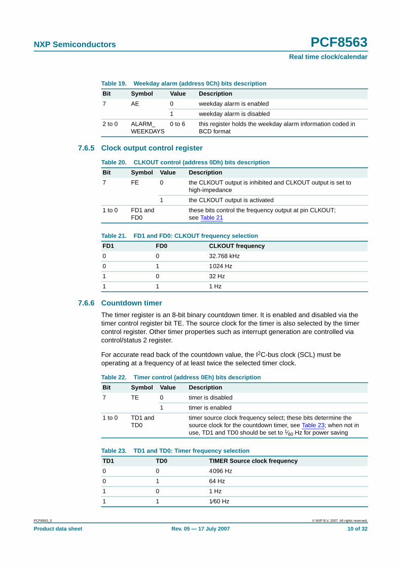
7.6.5 Clock output control register
7.6.6 Countdown timer
The timer register is an 8-bit binary countdown timer. It is enabled and disabled via thetimer control register bit TE. The source clock for the timer is also selected by the timercontrol register. Other timer properties such as interrupt generation are controlled viacontrol/status 2 register.
For accurate read back of the countdown value, the I2C-bus clock (SCL) must beoperating at a frequency of at least twice the selected timer clock.
Table 19. Weekday alarm (address 0Ch) bits description
Bit Symbol Value Description
7 AE 0 weekday alarm is enabled
1 weekday alarm is disabled
2 to 0 ALARM_WEEKDAYS
0 to 6 this register holds the weekday alarm information coded inBCD format
Table 20. CLKOUT control (address 0Dh) bits description
Bit Symbol Value Description
7 FE 0 the CLKOUT output is inhibited and CLKOUT output is set tohigh-impedance
1 the CLKOUT output is activated
1 to 0 FD1 andFD0
these bits control the frequency output at pin CLKOUT;see Table 21
Table 21. FD1 and FD0: CLKOUT frequency selection
FD1 FD0 CLKOUT frequency
0 0 32.768 kHz
0 1 1024 Hz
1 0 32 Hz
1 1 1 Hz
Table 22. Timer control (address 0Eh) bits description
Bit Symbol Value Description
7 TE 0 timer is disabled
1 timer is enabled
1 to 0 TD1 andTD0
timer source clock frequency select; these bits determine thesource clock for the countdown timer, see Table 23; when not inuse, TD1 and TD0 should be set to 1⁄60 Hz for power saving
Table 23. TD1 and TD0: Timer frequency selection
TD1 TD0 TIMER Source clock frequency
0 0 4096 Hz
0 1 64 Hz
1 0 1 Hz
1 1 1⁄60 Hz
PCF8563_5 © NXP B.V. 2007. All rights reserved.
Product data sheet Rev. 05 — 17 July 2007 10 of 32

NXP Semiconductors PCF8563Real time clock/calendar
7.7 EXT_CLK test modeA test mode is available which allows for on-board testing. In such a mode it is possible toset up test conditions and control the operation of the RTC.
The test mode is entered by setting bit TEST1 in control/status1 register. Thenpin CLKOUT becomes an input. The test mode replaces the internal 64 Hz signal with thesignal applied to pin CLKOUT. Every 64 positive edges applied to pin CLKOUT will thengenerate an increment of one second.
The signal applied to pin CLKOUT should have a minimum pulse width of 300 ns and aminimum period of 1000 ns. The internal 64 Hz clock, now sourced from CLKOUT, isdivided down to 1 Hz by a 26 divide chain called a pre-scaler. The pre-scaler can be setinto a known state by using bit STOP. When bit STOP is set, the pre-scaler is reset to 0(STOP must be cleared before the pre-scaler can operate again).
From a STOP condition, the first 1 second increment will take place after 32 positiveedges on CLKOUT. Thereafter, every 64 positive edges will cause a 1 second increment.
Remark: Entry into EXT_CLK test mode is not synchronized to the internal 64 Hz clock.When entering the test mode, no assumption as to the state of the pre-scaler can bemade.
Operation example:
1. Set EXT_CLK test mode (control/status 1, bit TEST1 = 1)
2. Set STOP (control/status 1, bit STOP = 1)
3. Clear STOP (control/status 1, bit STOP = 0)
4. Set time registers to desired value
5. Apply 32 clock pulses to CLKOUT
6. Read time registers to see the first change
7. Apply 64 clock pulses to CLKOUT
8. Read time registers to see the second change
Repeat 7 and 8 for additional increments.
7.8 Power-On Reset (POR) overrideThe POR duration is directly related to the crystal oscillator start-up time. Due to the longstart-up times experienced by these types of circuits, a mechanism has been built in todisable the POR and hence speed up on-board test of the device. The setting of this moderequires that the I2C-bus pins, SDA and SCL, be toggled in a specific order as shown inFigure 8. All timings are required minimums.
Table 24. Timer (address 0Fh) bits description
Bit Symbol Value Description
7 to 0 TIMER 00h to FFh countdown value = n;
CountdownPeriodn
SourceClockFrequency---------------------------------------------------------------=
PCF8563_5 © NXP B.V. 2007. All rights reserved.
Product data sheet Rev. 05 — 17 July 2007 11 of 32

NXP Semiconductors PCF8563Real time clock/calendar
Once the override mode has been entered, the device immediately stops being reset andnormal operation may commence i.e. entry into the EXT_CLK test mode via I2C-busaccess. The override mode may be cleared by writing a logic 0 to TESTC. TESTC must beset to logic 1 before re-entry into the override mode is possible. Setting TESTC to logic 0during normal operation has no effect except to prevent entry into the POR override mode.
Table 25 shows the register reset values.
[1] registers marked ‘x’ are undefined at power-up and unchanged by subsequent resets.
8. Characteristics of the I 2C-bus
The I2C-bus is for bidirectional, two-line communication between different ICs or modules.The two lines are a serial data line (SDA) and a serial clock line (SCL). Both lines must beconnected to a positive supply via a pull-up resistor. Data transfer may be initiated onlywhen the bus is not busy.
Fig 8. POR override sequence
mgm664
SCL
500 ns 2000 ns
SDA
8 ms
override activepower up
Table 25: Register reset value [1]
Address Register name Bit 7 Bit 6 Bit 5 Bit 4 Bit 3 Bit 2 Bit 1 Bit 0
00h control/status 1 0 0 0 0 1 0 0 0
01h control/status 2 x x 0 0 0 0 0 0
02h seconds 1 x x x x x x x
03h minutes 1 x x x x x x x
04h hours x x x x x x x x
05h days x x x x x x x x
06h weekdays x x x x x x x x
07h months/century x x x x x x x x
08h years x x x x x x x x
09h minute alarm 1 x x x x x x x
0Ah hour alarm 1 x x x x x x x
0Bh day alarm 1 x x x x x x x
0Ch weekday alarm 1 x x x x x x x
0Dh CLKOUT control 1 x x x x x 0 0
0Eh timer control 0 x x x x x 1 1
0Fh timer x x x x x x x x
PCF8563_5 © NXP B.V. 2007. All rights reserved.
Product data sheet Rev. 05 — 17 July 2007 12 of 32

NXP Semiconductors PCF8563Real time clock/calendar
8.1 Bit transferOne data bit is transferred during each clock pulse. The data on the SDA line must remainstable during the HIGH period of the clock pulse as changes in the data line at this timewill be interpreted as a control signal (see Figure 9).
8.2 Start and stop conditionsBoth data and clock lines remain HIGH when the bus is not busy. A HIGH-to-LOWtransition of the data line, while the clock is HIGH is defined as the START condition (S). ALOW-to-HIGH transition of the data line while the clock is HIGH is defined as the STOPcondition (P); see Figure 10.
8.3 System configurationA device generating a message is a transmitter, a device receiving a message is thereceiver. The device that controls the message is the master and the devices which arecontrolled by the master are the slaves (see Figure 11).
Fig 9. Bit transfer
mbc621
data linestable;
data valid
changeof dataallowed
SDA
SCL
Fig 10. Definition of start and stop conditions
mbc622
SDA
SCLP
STOP condition
SDA
SCLS
START condition
Fig 11. System configuration
mba605
MASTERTRANSMITTER /
RECEIVER
SLAVERECEIVER
SLAVETRANSMITTER /
RECEIVER
MASTERTRANSMITTER
MASTERTRANSMITTER /
RECEIVER
SDA
SCL
PCF8563_5 © NXP B.V. 2007. All rights reserved.
Product data sheet Rev. 05 — 17 July 2007 13 of 32

NXP Semiconductors PCF8563Real time clock/calendar
8.4 AcknowledgeThe number of data bytes transferred between the START and STOP conditions fromtransmitter to receiver is unlimited. Each byte of eight bits is followed by an acknowledgebit. The acknowledge bit is a HIGH-level signal put on the bus by the transmitter duringwhich time the master generates an extra acknowledge related clock pulse. A slavereceiver which is addressed must generate an acknowledge after the reception of eachbyte. Also a master receiver must generate an acknowledge after the reception of eachbyte that has been clocked out of the slave transmitter (see Figure 12).
The device that acknowledges must pull down the SDA line during the acknowledge clockpulse, so that the SDA line is stable LOW during the HIGH period of the acknowledgerelated clock pulse (set-up and hold times must be taken into consideration). A masterreceiver must signal an end of data to the transmitter by not generating an acknowledgeon the last byte that has been clocked out of the slave. In this event the transmitter mustleave the data line HIGH to enable the master to generate a stop condition.
8.5 I2C-bus protocol
8.5.1 Addressing
Before any data is transmitted on the I2C-bus, the device which should respond isaddressed first. The addressing is always carried out with the first byte transmitted afterthe start procedure.
The PCF8563 acts as a slave receiver or slave transmitter. Therefore the clock signal SCLis only an input signal, but the data signal SDA is a bidirectional line.
The PCF8563 slave address is shown in Figure 13.
Fig 12. Acknowledgement on the I 2C-bus
mbc602
S
STARTcondition
9821
clock pulse foracknowledgement
not acknowledge
acknowledge
data outputby transmitter
data outputby receiver
SCL frommaster
Fig 13. Slave address
mce189
1 0 1 0 0 0 1 R/W
group 1 group 2
PCF8563_5 © NXP B.V. 2007. All rights reserved.
Product data sheet Rev. 05 — 17 July 2007 14 of 32

NXP Semiconductors PCF8563Real time clock/calendar
8.5.2 Clock/calendar read/write cycles
The I2C-bus configuration for the different PCF8563 read and write cycles is shown inFigure 14, Figure 15 and Figure 16. The word address is a 4-bit value that defines whichregister is to be accessed next. The upper four bits of the word address are not used.
Fig 14. Master transmits to slave receiver (write mode)
S 0 ASLAVE ADDRESS WORD ADDRESS A ADATA P
acknowledgementfrom slave
acknowledgementfrom slave
acknowledgementfrom slave
R/W
auto incrementmemory word address
mbd822
n bytes
Fig 15. Master reads after setting word address (write word address; read data)
S 0 ASLAVE ADDRESS WORD ADDRESS A ASLAVE ADDRESS
acknowledgementfrom slave
acknowledgementfrom slave
acknowledgementfrom slave
R/W
acknowledgementfrom master
ADATA
auto incrementmemory word address
001aag133
P
no acknowledgementfrom master
1DATA
auto incrementmemory word address
last byte
R/W
S 1
n bytesat this moment master transmitter
becomes master receiver andPCA8563 slave receiver
becomes slave transmitter
Fig 16. Master reads slave immediately after first byte (read mode)
S 1 ASLAVE ADDRESS DATA A 1DATA
acknowledgementfrom slave
acknowledgementfrom master
no acknowledgementfrom master
R/W
auto incrementword address
mgl665
auto incrementword address
n bytes last byte
P
PCF8563_5 © NXP B.V. 2007. All rights reserved.
Product data sheet Rev. 05 — 17 July 2007 15 of 32

NXP Semiconductors PCF8563Real time clock/calendar
9. Limiting values
10. Static characteristics
Table 26. Limiting valuesIn accordance with the Absolute Maximum Rating System (IEC 60134)
Symbol Parameter Min Max Unit
VDD supply voltage −0.5 +6.5 V
IDD supply current −50 +50 mA
VI input voltage on pins SCL and SDA −0.5 +6.5 V
input voltage on pin OSCI −0.5 VDD + 0.5 V
VO output voltage on pins CLOCKOUTand INT
−0.5 +6.5 V
II DC input current at any input −10 +10 mA
IO DC output current at any output −10 +10 mA
Ptot total power dissipation - 300 mW
Tamb ambient temperature −40 +85 °C
Tstg storage temperature −65 +150 °C
Table 27. Static characteristicsVDD = 1.8 V to 5.5 V; VSS = 0 V; Tamb = −40 °C to +85 °C; fosc = 32.768 kHz; quartz Rs = 40 kΩ; CL = 8 pF; unless otherwisespecified.
Symbol Parameter Conditions Min Typ Max Unit
Supplies
VDD supply voltage interface inactive; fSCL = 0 Hz;Tamb = 25 °C; see Figure 20
[1] 1.0 - 5.5 V
interface active;fSCL = 400 kHz; see Figure 20
[1] 1.8 - 5.5 V
clock data integrity;Tamb = 25 °C
Vlow - 5.5 V
IDD1 supply current 1 interface active; see Figure 19
fSCL = 400 kHz - - 800 µA
fSCL = 100 kHz - - 200 µA
IDD2 supply current 2 interface inactive (fSCL = 0 Hz);CLKOUT disabled;Tamb = 25 °C; see Figure 17
[2]
VDD = 5.0 V - 275 550 nA
VDD = 3.0 V - 250 500 nA
VDD = 2.0 V - 225 450 nA
interface inactive (fSCL = 0 Hz);CLKOUT disabled;Tamb = −40 °C to +85 °C;see Figure 17
[2]
VDD = 5.0 V - 500 750 nA
VDD = 3.0 V - 400 650 nA
VDD = 2.0 V - 400 600 nA
PCF8563_5 © NXP B.V. 2007. All rights reserved.
Product data sheet Rev. 05 — 17 July 2007 16 of 32

NXP Semiconductors PCF8563Real time clock/calendar
[1] For reliable oscillator start-up at power-up: VDD(min)power-up = VDD(min) + 0.3 V.
[2] Timer source clock = 1⁄60 Hz, level of pins SCL and SDA is VDD or VSS.
[3] Tested on sample basis.
[4] See Figure 7.
IDD3 supply current 3 interface inactive (fSCL = 0 Hz);CLKOUT enabled at 32 kHz;Tamb = 25 °C; see Figure 18
[2]
VDD = 5.0 V - 825 1600 nA
VDD = 3.0 V - 550 1000 nA
VDD = 2.0 V - 425 800 nA
interface inactive (fSCL = 0 Hz);CLKOUT enabled at 32 kHz;Tamb = −40 °C to +85 °C;see Figure 18
[2]
VDD = 5.0 V - 950 1700 nA
VDD = 3.0 V - 650 1100 nA
VDD = 2.0 V - 500 900 nA
Inputs
VIL LOW-level input voltage VSS - 0.3VDD V
VIH HIGH-level input voltage 0.7VDD - VDD V
ILI input leakage current VI = VDD or VSS −1 0 +1 µA
Ci input capacitance [3] - - 7 pF
Outputs
IOL(SDA) SDA LOW-level outputcurrent
VOL = 0.4 V; VDD = 5 V −3 - - mA
IOL(INT) INT LOW-level outputcurrent
VOL = 0.4 V; VDD = 5 V −1 - - mA
IOL(CLKOUT) CLKOUT LOW-leveloutput current
VOL = 0.4 V; VDD = 5 V −1 - - mA
IOH(CLKOUT) CLKOUT HIGH-leveloutput current
VOH = 4.6 V; VDD = 5 V 1 - - mA
ILO output leakage current VO = VDD or VSS −1 0 +1 µA
Voltage detector
Vlow low voltage detection Tamb = 25 °C; VL set voltage [4] - 0.9 1.0 V
Table 27. Static characteristics …continuedVDD = 1.8 V to 5.5 V; VSS = 0 V; Tamb = −40 °C to +85 °C; fosc = 32.768 kHz; quartz Rs = 40 kΩ; CL = 8 pF; unless otherwisespecified.
Symbol Parameter Conditions Min Typ Max Unit
PCF8563_5 © NXP B.V. 2007. All rights reserved.
Product data sheet Rev. 05 — 17 July 2007 17 of 32

NXP Semiconductors PCF8563Real time clock/calendar
Tamb = 25 °C; Timer = 1 minute. Tamb = 25 °C; Timer = 1 minute.
Fig 17. IDD as a function of V DD; CLKOUT disabled Fig 18. I DD as a function of V DD; CLKOUT = 32 kHz
VDD = 3 V; Timer = 1 minute. Tamb = 25 °C; normalized to VDD = 3 V.
Fig 19. IDD as a function of T; CLKOUT = 32 kHz Fig 20. Frequency deviation as a function of V DD
0 2 6
mgr888
4 VDD (V)
1
0
0.4
0.2
0.8
0.6
IDD(mA)
0 2 6
mgr889
4 VDD (V)
1
0
0.4
0.2
0.8
0.6
IDD(mA)
−40 0 40 120
mgr890
80 T (°C)
1
0
0.4
0.2
0.8
0.6
IDD(mA)
0 2 6
4
2
−4
−2
0
mgr891
4 VDD (V)
frequencydeviation
(ppm)
PCF8563_5 © NXP B.V. 2007. All rights reserved.
Product data sheet Rev. 05 — 17 July 2007 18 of 32
NXP Semiconductors PCF8563Real time clock/calendar
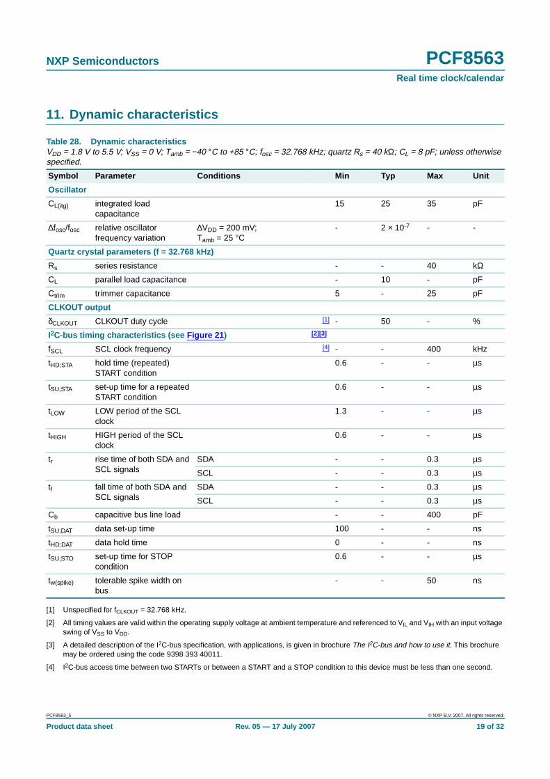
11. Dynamic characteristics
[1] Unspecified for fCLKOUT = 32.768 kHz.
[2] All timing values are valid within the operating supply voltage at ambient temperature and referenced to VIL and VIH with an input voltageswing of VSS to VDD.
[3] A detailed description of the I2C-bus specification, with applications, is given in brochure The I2C-bus and how to use it. This brochuremay be ordered using the code 9398 393 40011.
[4] I2C-bus access time between two STARTs or between a START and a STOP condition to this device must be less than one second.
Table 28. Dynamic characteristicsVDD = 1.8 V to 5.5 V; VSS = 0 V; Tamb = −40 °C to +85 °C; fosc = 32.768 kHz; quartz Rs = 40 kΩ; CL = 8 pF; unless otherwisespecified.
Symbol Parameter Conditions Min Typ Max Unit
Oscillator
CL(itg) integrated loadcapacitance
15 25 35 pF
∆fosc/fosc relative oscillatorfrequency variation
∆VDD = 200 mV;Tamb = 25 °C
- 2 × 10⁻⁷ - -
Quartz crystal parameters (f = 32.768 kHz)
Rs series resistance - - 40 kΩ
CL parallel load capacitance - 10 - pF
Ctrim trimmer capacitance 5 - 25 pF
CLKOUT output
δCLKOUT CLKOUT duty cycle [1] - 50 - %
I2C-bus timing characteristics (see Figure 21) [2] [3]
fSCL SCL clock frequency [4] - - 400 kHz
tHD;STA hold time (repeated)START condition
0.6 - - µs
tSU;STA set-up time for a repeatedSTART condition
0.6 - - µs
tLOW LOW period of the SCLclock
1.3 - - µs
tHIGH HIGH period of the SCLclock
0.6 - - µs
tr rise time of both SDA andSCL signals
SDA - - 0.3 µs
SCL - - 0.3 µs
tf fall time of both SDA andSCL signals
SDA - - 0.3 µs
SCL - - 0.3 µs
Cb capacitive bus line load - - 400 pF
tSU;DAT data set-up time 100 - - ns
tHD;DAT data hold time 0 - - ns
tSU;STO set-up time for STOPcondition
0.6 - - µs
tw(spike) tolerable spike width onbus
- - 50 ns
PCF8563_5 © NXP B.V. 2007. All rights reserved.
Product data sheet Rev. 05 — 17 July 2007 19 of 32

NXP Semiconductors PCF8563Real time clock/calendar
12. Application information
Fig 21. I2C-bus timing waveforms
SDA
mga728
SDA
SCL
tSU;STAtSU;STO
tHD;STA
tBUF tLOW
tHD;DAT tHIGHtr
tf
tSU;DAT
Fig 22. Application diagram
mgm665
SCL
SDAVSS
OSCI
OSCO
CLOCK CALENDAR
PCF8563
SDA
SCL
MASTERTRANSMITTER/
RECEIVER
VDD
VDD
SDA SCL
R R
VDD
(I2C-bus)
R: pull-up resistor
R =
1 F
trCb
PCF8563_5 © NXP B.V. 2007. All rights reserved.
Product data sheet Rev. 05 — 17 July 2007 20 of 32

NXP Semiconductors PCF8563Real time clock/calendar
12.1 Quartz frequency adjustment
12.1.1 Method 1: fixed OSCI capacitor
By evaluating the average capacitance necessary for the application layout, a fixedcapacitor can be used. The frequency is best measured via the 32.768 kHz signalavailable after power-on at pin CLKOUT. The frequency tolerance depends on the quartzcrystal tolerance, the capacitor tolerance and the device-to-device tolerance (on average±5 × 10⁻⁶). Average deviations of ±5 minutes per year can be easily achieved.
12.1.2 Method 2: OSCI trimmer
Using the 32.768 kHz signal available after power-on at pin CLKOUT, fast setting of atrimmer is possible.
12.1.3 Method 3: OSCO output
Direct measurement of OSCO out (accounting for test probe capacitance).
PCF8563_5 © NXP B.V. 2007. All rights reserved.
Product data sheet Rev. 05 — 17 July 2007 21 of 32

NXP Semiconductors PCF8563Real time clock/calendar
13. Package outline
Fig 23. Package outline SOT97-1
REFERENCESOUTLINEVERSION
EUROPEANPROJECTION ISSUE DATE
IEC JEDEC JEITA
SOT97-199-12-2703-02-13
UNIT Amax.
1 2 b1(1) (1) (1)
b2 c D E e M ZHL
mm
DIMENSIONS (inch dimensions are derived from the original mm dimensions)
A min.
A max. b
max.wMEe1
1.731.14
0.530.38
0.360.23
9.89.2
6.486.20
3.603.05
0.2542.54 7.628.257.80
10.08.3
1.154.2 0.51 3.2
inches 0.0680.045
0.0210.015
0.0140.009
1.070.89
0.0420.035
0.390.36
0.260.24
0.140.12
0.010.1 0.30.320.31
0.390.33
0.0450.17 0.02 0.13
b2
050G01 MO-001 SC-504-8
MH
c
(e )1
ME
A
L
seat
ing
plan
e
A1
w Mb1
e
D
A2
Z
8
1
5
4
b
E
0 5 10 mm
scale
Note
1. Plastic or metal protrusions of 0.25 mm (0.01 inch) maximum per side are not included.
pin 1 index
DIP8: plastic dual in-line package; 8 leads (300 mil) SOT97-1
PCF8563_5 © NXP B.V. 2007. All rights reserved.
Product data sheet Rev. 05 — 17 July 2007 22 of 32

NXP Semiconductors PCF8563Real time clock/calendar
Fig 24. Package outline SOT96-1
UNITA
max. A1 A2 A3 bp c D(1) E(2) (1)e HE L L p Q Zywv θ
REFERENCESOUTLINEVERSION
EUROPEANPROJECTION ISSUE DATE
IEC JEDEC JEITA
mm
inches
1.750.250.10
1.451.25
0.250.490.36
0.250.19
5.04.8
4.03.8
1.276.25.8
1.050.70.6
0.70.3 8
0
o
o
0.25 0.10.25
DIMENSIONS (inch dimensions are derived from the original mm dimensions)
Notes
1. Plastic or metal protrusions of 0.15 mm (0.006 inch) maximum per side are not included.
2. Plastic or metal protrusions of 0.25 mm (0.01 inch) maximum per side are not included.
1.00.4
SOT96-1
X
w M
θ
AA1
A2
bp
D
HE
Lp
Q
detail X
E
Z
e
c
L
v M A
(A )3
A
4
5
pin 1 index
1
8
y
076E03 MS-012
0.0690.0100.004
0.0570.049
0.010.0190.014
0.01000.0075
0.200.19
0.160.15
0.050.2440.228
0.0280.024
0.0280.012
0.010.010.041 0.0040.0390.016
0 2.5 5 mm
scale
SO8: plastic small outline package; 8 leads; body width 3.9 mm SOT96-1
99-12-2703-02-18
PCF8563_5 © NXP B.V. 2007. All rights reserved.
Product data sheet Rev. 05 — 17 July 2007 23 of 32

NXP Semiconductors PCF8563Real time clock/calendar
Fig 25. Package outline SOT505-1
UNIT A1A
max.A2 A3 bp LHE Lp w yvc eD(1) E(2) Z(1) θ
REFERENCESOUTLINEVERSION
EUROPEANPROJECTION ISSUE DATE
IEC JEDEC JEITA
mm 0.150.05
0.950.80
0.450.25
0.280.15
3.12.9
3.12.9
0.655.14.7
0.700.35
6°0°
0.1 0.10.10.94
DIMENSIONS (mm are the original dimensions)
Notes
1. Plastic or metal protrusions of 0.15 mm maximum per side are not included.
2. Plastic or metal protrusions of 0.25 mm maximum per side are not included.
0.70.4
SOT505-1 99-04-0903-02-18
w Mbp
D
Z
e
0.25
1 4
8 5
θ
AA2A1
Lp
(A3)
detail X
L
HE
E
c
v M A
XA
y
2.5 5 mm0
scale
TSSOP8: plastic thin shrink small outline package; 8 leads; body width 3 mm SOT505-1
1.1
pin 1 index
PCF8563_5 © NXP B.V. 2007. All rights reserved.
Product data sheet Rev. 05 — 17 July 2007 24 of 32

NXP Semiconductors PCF8563Real time clock/calendar
Fig 26. Package outline SOT650-1
0.50.210.050.00
A1 EhbUNIT D(1) ye
2
e1
REFERENCESOUTLINEVERSION
EUROPEANPROJECTION ISSUE DATE
IEC JEDEC JEITA
mm 3.12.9
c Dh
1.751.45
y1
3.12.9
2.552.15
0.300.18
0.05 0.1
DIMENSIONS (mm are the original dimensions)
SOT650-1 MO-229 - - -- - -
E(1)
0.550.30
L
0.1
v
0.05
w
0 2 mm1
scale
SOT650-1HVSON10: plastic thermal enhanced very thin small outline package; no leads;10 terminals; body 3 x 3 x 0.85 mm
A(1)
max.
AA1
c
detail X
y
Dh
Eh
e
L
10
51
6
D
E
y1 C
C
B A
01-01-2202-02-08
terminal 1index area
terminal 1index area
X
e1
b ACC
Bv M
w M
Note
1. Plastic or metal protrusions of 0.075 mm maximum per side are not included.
PCF8563_5 © NXP B.V. 2007. All rights reserved.
Product data sheet Rev. 05 — 17 July 2007 25 of 32

NXP Semiconductors PCF8563Real time clock/calendar
14. Handling information
Inputs and outputs are protected against electrostatic discharge in normal handling.However, to be completely safe you must take normal precautions appropriate to handlingMOS devices; see JESD625-A and/or IEC61340-5.
15. Soldering
This text provides a very brief insight into a complex technology. A more in-depth accountof soldering ICs can be found in Application Note AN10365 “Surface mount reflowsoldering description”.
15.1 Introduction to solderingSoldering is one of the most common methods through which packages are attached toPrinted Circuit Boards (PCBs), to form electrical circuits. The soldered joint provides boththe mechanical and the electrical connection. There is no single soldering method that isideal for all IC packages. Wave soldering is often preferred when through-hole andSurface Mount Devices (SMDs) are mixed on one printed wiring board; however, it is notsuitable for fine pitch SMDs. Reflow soldering is ideal for the small pitches and highdensities that come with increased miniaturization.
15.2 Wave and reflow solderingWave soldering is a joining technology in which the joints are made by solder coming froma standing wave of liquid solder. The wave soldering process is suitable for the following:
• Through-hole components
• Leaded or leadless SMDs, which are glued to the surface of the printed circuit board
Not all SMDs can be wave soldered. Packages with solder balls, and some leadlesspackages which have solder lands underneath the body, cannot be wave soldered. Also,leaded SMDs with leads having a pitch smaller than ~0.6 mm cannot be wave soldered,due to an increased probability of bridging.
The reflow soldering process involves applying solder paste to a board, followed bycomponent placement and exposure to a temperature profile. Leaded packages,packages with solder balls, and leadless packages are all reflow solderable.
Key characteristics in both wave and reflow soldering are:
• Board specifications, including the board finish, solder masks and vias
• Package footprints, including solder thieves and orientation
• The moisture sensitivity level of the packages
• Package placement
• Inspection and repair
• Lead-free soldering versus PbSn soldering
15.3 Wave solderingKey characteristics in wave soldering are:
PCF8563_5 © NXP B.V. 2007. All rights reserved.
Product data sheet Rev. 05 — 17 July 2007 26 of 32

NXP Semiconductors PCF8563Real time clock/calendar
• Process issues, such as application of adhesive and flux, clinching of leads, boardtransport, the solder wave parameters, and the time during which components areexposed to the wave
• Solder bath specifications, including temperature and impurities
15.4 Reflow solderingKey characteristics in reflow soldering are:
• Lead-free versus SnPb soldering; note that a lead-free reflow process usually leads tohigher minimum peak temperatures (see Figure 27) than a PbSn process, thusreducing the process window
• Solder paste printing issues including smearing, release, and adjusting the processwindow for a mix of large and small components on one board
• Reflow temperature profile; this profile includes preheat, reflow (in which the board isheated to the peak temperature) and cooling down. It is imperative that the peaktemperature is high enough for the solder to make reliable solder joints (a solder pastecharacteristic). In addition, the peak temperature must be low enough that thepackages and/or boards are not damaged. The peak temperature of the packagedepends on package thickness and volume and is classified in accordance withTable 29 and 30
Moisture sensitivity precautions, as indicated on the packing, must be respected at alltimes.
Studies have shown that small packages reach higher temperatures during reflowsoldering, see Figure 27.
Table 29. SnPb eutectic process (from J-STD-020C)
Package thickness (mm) Package reflow temperature ( °C)
Volume (mm 3)
< 350 ≥ 350
< 2.5 235 220
≥ 2.5 220 220
Table 30. Lead-free process (from J-STD-020C)
Package thickness (mm) Package reflow temperature ( °C)
Volume (mm 3)
< 350 350 to 2000 > 2000
< 1.6 260 260 260
1.6 to 2.5 260 250 245
> 2.5 250 245 245
PCF8563_5 © NXP B.V. 2007. All rights reserved.
Product data sheet Rev. 05 — 17 July 2007 27 of 32

NXP Semiconductors PCF8563Real time clock/calendar
For further information on temperature profiles, refer to Application Note AN10365“Surface mount reflow soldering description”.
MSL: Moisture Sensitivity Level
Fig 27. Temperature profiles for large and small components
001aac844
temperature
time
minimum peak temperature= minimum soldering temperature
maximum peak temperature= MSL limit, damage level
peak temperature
PCF8563_5 © NXP B.V. 2007. All rights reserved.
Product data sheet Rev. 05 — 17 July 2007 28 of 32
NXP Semiconductors PCF8563Real time clock/calendar
16. Revision history
Table 31. Revision history
Document ID Release date Data sheet status Change notice Supersedes
PCF8563_5 20070717 Product data sheet - PCF8563-04
Modifications: • The format of this data sheet has been redesigned to comply with the new identity guidelinesof NXP Semiconductors.
• Legal texts have been adapted to the new company name where appropriate.
• Quick reference data table removed to comply with guidelines.
• Table 3: Table 3 and Table 4 combined in one table.
• Section 4: added topside mark.
• Section 4: added HVSO10 package.
PCF8563-04(9397 750 12999)
20040312 Product data - PCF8563-03
Modifications: • Section 4: Corrections in the unit column of Table 1
PCF8563-03(9397 750 11158)
20030414 Product data - PCF8563-02
PCF8563-02(9397 750 04855)
19990416 Product data - PCF8563_N_1
PCF8563_N_1(9397 750 03282)
19980325 Objective specification - -
PCF8563_5 © NXP B.V. 2007. All rights reserved.
Product data sheet Rev. 05 — 17 July 2007 29 of 32
NXP Semiconductors PCF8563Real time clock/calendar
17. Legal information
17.1 Data sheet status
[1] Please consult the most recently issued document before initiating or completing a design.
[2] The term ‘short data sheet’ is explained in section “Definitions”.
[3] The product status of device(s) described in this document may have changed since this document was published and may differ in case of multiple devices. The latest product statusinformation is available on the Internet at URL http://www.nxp.com.
17.2 Definitions
Draft — The document is a draft version only. The content is still underinternal review and subject to formal approval, which may result inmodifications or additions. NXP Semiconductors does not give anyrepresentations or warranties as to the accuracy or completeness ofinformation included herein and shall have no liability for the consequences ofuse of such information.
Short data sheet — A short data sheet is an extract from a full data sheetwith the same product type number(s) and title. A short data sheet is intendedfor quick reference only and should not be relied upon to contain detailed andfull information. For detailed and full information see the relevant full datasheet, which is available on request via the local NXP Semiconductors salesoffice. In case of any inconsistency or conflict with the short data sheet, thefull data sheet shall prevail.
17.3 Disclaimers
General — Information in this document is believed to be accurate andreliable. However, NXP Semiconductors does not give any representations orwarranties, expressed or implied, as to the accuracy or completeness of suchinformation and shall have no liability for the consequences of use of suchinformation.
Right to make changes — NXP Semiconductors reserves the right to makechanges to information published in this document, including withoutlimitation specifications and product descriptions, at any time and withoutnotice. This document supersedes and replaces all information supplied priorto the publication hereof.
Suitability for use — NXP Semiconductors products are not designed,authorized or warranted to be suitable for use in medical, military, aircraft,space or life support equipment, nor in applications where failure ormalfunction of a NXP Semiconductors product can reasonably be expected to
result in personal injury, death or severe property or environmental damage.NXP Semiconductors accepts no liability for inclusion and/or use of NXPSemiconductors products in such equipment or applications and thereforesuch inclusion and/or use is at the customer’s own risk.
Applications — Applications that are described herein for any of theseproducts are for illustrative purposes only. NXP Semiconductors makes norepresentation or warranty that such applications will be suitable for thespecified use without further testing or modification.
Limiting values — Stress above one or more limiting values (as defined inthe Absolute Maximum Ratings System of IEC 60134) may cause permanentdamage to the device. Limiting values are stress ratings only and operation ofthe device at these or any other conditions above those given in theCharacteristics sections of this document is not implied. Exposure to limitingvalues for extended periods may affect device reliability.
Terms and conditions of sale — NXP Semiconductors products are soldsubject to the general terms and conditions of commercial sale, as publishedat http://www.nxp.com/profile/terms, including those pertaining to warranty,intellectual property rights infringement and limitation of liability, unlessexplicitly otherwise agreed to in writing by NXP Semiconductors. In case ofany inconsistency or conflict between information in this document and suchterms and conditions, the latter will prevail.
No offer to sell or license — Nothing in this document may be interpretedor construed as an offer to sell products that is open for acceptance or thegrant, conveyance or implication of any license under any copyrights, patentsor other industrial or intellectual property rights.
17.4 TrademarksNotice: All referenced brands, product names, service names and trademarksare the property of their respective owners.
I2C-bus — logo is a trademark of NXP B.V.
18. Contact information
For additional information, please visit: http://www .nxp.com
For sales office addresses, send an email to: salesad [email protected]
Document status [1] [2] Product status [3] Definition
Objective [short] data sheet Development This document contains data from the objective specification for product development.
Preliminary [short] data sheet Qualification This document contains data from the preliminary specification.
Product [short] data sheet Production This document contains the product specification.
PCF8563_5 © NXP B.V. 2007. All rights reserved.
Product data sheet Rev. 05 — 17 July 2007 30 of 32

NXP Semiconductors PCF8563Real time clock/calendar
Notes
PCF8563_5 © NXP B.V. 2007. All rights reserved.
Product data sheet Rev. 05 — 17 July 2007 31 of 32

NXP Semiconductors PCF8563Real time clock/calendar
19. Contents
1 General description . . . . . . . . . . . . . . . . . . . . . . 12 Features . . . . . . . . . . . . . . . . . . . . . . . . . . . . . . . 13 Applications . . . . . . . . . . . . . . . . . . . . . . . . . . . . 14 Ordering information . . . . . . . . . . . . . . . . . . . . . 25 Block diagram . . . . . . . . . . . . . . . . . . . . . . . . . . 26 Pinning information . . . . . . . . . . . . . . . . . . . . . . 36.1 Pinning . . . . . . . . . . . . . . . . . . . . . . . . . . . . . . . 36.2 Pin description . . . . . . . . . . . . . . . . . . . . . . . . . 47 Functional description . . . . . . . . . . . . . . . . . . . 47.1 Alarm function modes. . . . . . . . . . . . . . . . . . . . 47.2 Timer. . . . . . . . . . . . . . . . . . . . . . . . . . . . . . . . . 57.3 Clock output . . . . . . . . . . . . . . . . . . . . . . . . . . . 57.4 Reset . . . . . . . . . . . . . . . . . . . . . . . . . . . . . . . . 57.5 Voltage-low detector . . . . . . . . . . . . . . . . . . . . . 57.6 Register organization . . . . . . . . . . . . . . . . . . . . 67.6.1 Control/status 1 register . . . . . . . . . . . . . . . . . . 67.6.2 Control/status 2 register . . . . . . . . . . . . . . . . . . 67.6.3 Time and date registers . . . . . . . . . . . . . . . . . . 77.6.4 Alarm registers . . . . . . . . . . . . . . . . . . . . . . . . . 97.6.5 Clock output control register . . . . . . . . . . . . . . 107.6.6 Countdown timer. . . . . . . . . . . . . . . . . . . . . . . 107.7 EXT_CLK test mode. . . . . . . . . . . . . . . . . . . . 117.8 Power-On Reset (POR) override . . . . . . . . . . 118 Characteristics of the I 2C-bus. . . . . . . . . . . . . 128.1 Bit transfer . . . . . . . . . . . . . . . . . . . . . . . . . . . 138.2 Start and stop conditions . . . . . . . . . . . . . . . . 138.3 System configuration . . . . . . . . . . . . . . . . . . . 138.4 Acknowledge . . . . . . . . . . . . . . . . . . . . . . . . . 148.5 I2C-bus protocol . . . . . . . . . . . . . . . . . . . . . . . 148.5.1 Addressing . . . . . . . . . . . . . . . . . . . . . . . . . . . 148.5.2 Clock/calendar read/write cycles . . . . . . . . . . 159 Limiting values. . . . . . . . . . . . . . . . . . . . . . . . . 1610 Static characteristics. . . . . . . . . . . . . . . . . . . . 1611 Dynamic characteristics . . . . . . . . . . . . . . . . . 1912 Application information. . . . . . . . . . . . . . . . . . 2012.1 Quartz frequency adjustment . . . . . . . . . . . . . 2112.1.1 Method 1: fixed OSCI capacitor . . . . . . . . . . . 2112.1.2 Method 2: OSCI trimmer. . . . . . . . . . . . . . . . . 2112.1.3 Method 3: OSCO output . . . . . . . . . . . . . . . . . 2113 Package outline . . . . . . . . . . . . . . . . . . . . . . . . 2214 Handling information. . . . . . . . . . . . . . . . . . . . 2615 Soldering . . . . . . . . . . . . . . . . . . . . . . . . . . . . . 2615.1 Introduction to soldering . . . . . . . . . . . . . . . . . 2615.2 Wave and reflow soldering . . . . . . . . . . . . . . . 2615.3 Wave soldering . . . . . . . . . . . . . . . . . . . . . . . . 26
15.4 Reflow soldering. . . . . . . . . . . . . . . . . . . . . . . 2716 Revision history . . . . . . . . . . . . . . . . . . . . . . . 2917 Legal information . . . . . . . . . . . . . . . . . . . . . . 3017.1 Data sheet status . . . . . . . . . . . . . . . . . . . . . . 3017.2 Definitions . . . . . . . . . . . . . . . . . . . . . . . . . . . 3017.3 Disclaimers. . . . . . . . . . . . . . . . . . . . . . . . . . . 3017.4 Trademarks . . . . . . . . . . . . . . . . . . . . . . . . . . 3018 Contact information . . . . . . . . . . . . . . . . . . . . 3019 Contents. . . . . . . . . . . . . . . . . . . . . . . . . . . . . . 32
© NXP B.V. 2007. All rights reserved.For more information, please visit: http://www.nxp.comFor sales office addresses, please send an email to: [email protected]
Date of release: 17 July 2007
Document identifier: PCF8563_5
Please be aware that important notices concerning this document and the product(s)described herein, have been included in section ‘Legal information’.