
PCB Mounting Guidelines for Surface Mount...
19
Atmel-8826B-SEEPROM-PCB-Mounting-Guidelines-Surface-Mount-Packages-ApplicationNote_042016 Introduction This document provides PCB designers with a set of guidelines for successful board mounting of Atmel ® surface mount packages. Package Land Pattern descriptions are depicted by the package family, and although each family is represented by a single body size and lead count, the individual land description apply to all packages within a particular family. Land Pattern descriptions were provided by IPC-7351 Calculator from the Mentor Graphics Corporation. These are only general guidelines that Atmel received from the IPC-7351 Calculator. The solder reflow guidelines are derived from IPC -9502. Atmel does not make direct recommendation for board design, nor does it take legal liability and responsibility for the information in this document. Please refer to the IPC website for more information regarding board design and processing. 1. Solder Reflow Process Figure 1-1 shows the typical process flow for mounting surface mount packages to printed circuit boards. It is important to include the post print and the post reflow inspection, especially during the process development. The volume of paste printed should be measured either by 2D or 3D techniques. The paste volume should be around 80% to 90% of the stencil aperture volume to indicate a good paste release. After reflow, the mounted package should be inspected by transmission x-ray for the presence of voids, solder balling, or other defects. Cross-sectioning may also be required to determine the fillet shape, size, and the joint standoff height during process development. A typical reflow profile for no-clean solder paste is shown in Figure 1-2, temperature measured at the solder joint. Figure 1-1. Typical PCB Mounting Process Flow Solder Paste Printing Component Placement Pre-Reflow Inspection Reflow Post Reflow Inspection (Visual/X-ray) Rework and Touch-up Post Print Inspection APPLICATION NOTE PCB Mounting Guidelines for Surface Mount Packages
Transcript of PCB Mounting Guidelines for Surface Mount...
APPLICATION NOTE
PCB Mounting Guidelines for Surface Mount Packages
Introduction
This document provides PCB designers with a set of guidelines for successful
board mounting of Atmel® surface mount packages. Package Land Pattern
descriptions are depicted by the package family, and although each family is
represented by a single body size and lead count, the individual land description
apply to all packages within a particular family. Land Pattern descriptions were
provided by IPC-7351 Calculator from the Mentor Graphics Corporation. These
are only general guidelines that Atmel received from the IPC-7351 Calculator. The
solder reflow guidelines are derived from IPC -9502. Atmel does not make direct
recommendation for board design, nor does it take legal liability and responsibility
for the information in this document. Please refer to the IPC website for more
information regarding board design and processing.
1. Solder Reflow Process
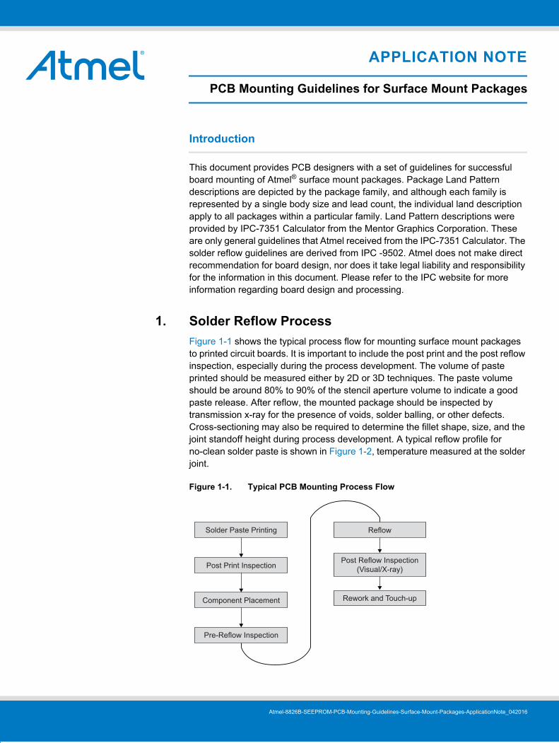
Figure 1-1 shows the typical process flow for mounting surface mount packages
to printed circuit boards. It is important to include the post print and the post reflow
inspection, especially during the process development. The volume of paste
printed should be measured either by 2D or 3D techniques. The paste volume
should be around 80% to 90% of the stencil aperture volume to indicate a good
paste release. After reflow, the mounted package should be inspected by
transmission x-ray for the presence of voids, solder balling, or other defects.
Cross-sectioning may also be required to determine the fillet shape, size, and the
joint standoff height during process development. A typical reflow profile for
no-clean solder paste is shown in Figure 1-2, temperature measured at the solder
joint.
Figure 1-1. Typical PCB Mounting Process Flow
Solder Paste Printing
Component Placement
Pre-Reflow Inspection
Reflow
Post Reflow Inspection(Visual/X-ray)
Rework and Touch-up
Post Print Inspection
Atmel-8826B-SEEPROM-PCB-Mounting-Guidelines-Surface-Mount-Packages-ApplicationNote_042016

1.1 Reflow Temperature Profiles
Since the actual reflow profile depends on the solder paste being used and the board density, Atmel does not
recommend a specific profile; however, the temperature should not exceed the maximum temperature the
package is qualified for according to the moisture sensitivity level. The time above the liquidus temperature
should be around 60 seconds, and the ramp rate during preheat should be 3C per second or lower.
Figure 1-2. Reliability Pb Free Profile
Note: Temperature value in boxes represents actual setting used in Atmel (CSO) Reliability Lab’s IR furnace for package
qualifications.
300
0
50
100
150
200
250
0 50 100 150 200 250
Tem
pera
ture
(o C)
Time (Seconds)
Atmel Reliability Pb Free (IR Furnace) Profile(for small packages - 8L SOIC, PDIP, TSSOP, SAP etc.)
Soak time 150°C to 200°C = 22.5sec Soak time, JEDEC 60sec to 80sec
200°C to 217°C Ramp 1.9°C/sJEDEC 3°C/s max
Time Above Liquidous 77 JEDEC 60sec to 150sec
217°C to 255°C Ramp 1.1°C/sJEDEC 3°C/s
Ramp Down 2.3°C/sJEDEC 6°C/s max
Time at 260°C = 12sec
Time at 255°C = 26.4secJEDEC 20sec to 40sec
PCB Mounting Guidelines for Surface Mount Packages [APPLICATION NOTE]Atmel-8826B-SEEPROM-PCB-Mounting-Guidelines-Surface-Mount-Packages-ApplicationNote_042016
2
2. Configurations for Packages with Thermal Pads
For devices to perform at their peak, special considerations are needed to properly design the board and to
mount the package. For enhanced thermal, electrical, and board level performance, the exposed pad on the
package needs to be soldered to the board using a corresponding thermal pad on the board. Furthermore, for
proper heat conduction through the board, thermal vias need to be incorporated in the PCB in the thermal pad
region. The PCB footprint design needs to be considered from dimensional tolerances due to the package,
PCB, and the assembly factors. A number of factors may have a significant effect on mounting the package on
the board and the quality of the solder joints.
Some of these factors include:
Amount of solder paste coverage in the thermal pad region
Stencil design for peripheral and thermal pad region
Type of vias
Board thickness
Copper thickness
Lead finish on the package
Surface finish on the board
Type of solder paste
Reflow profile
This document provides the guidelines for this purpose. It should be emphasized that this is just a guideline to
help the user in developing the proper board design and surface mount process. Actual studies as well as
development effort may be needed to optimize the process as per user's surface mount practices and
requirements.
2.1 Thermal Pad and Via Design
Some packages are designed to provide superior thermal performance. This is partly achieved by incorporating
an exposed die paddle on the bottom surface of the package; however, in order to take full advantage of this
feature, the PCB must have features to effectively conduct heat away from the package. This can be achieved
by incorporating a thermal pad and thermal vias on the PCB. While a thermal pad provides a solderable surface
on the top surface of the PCB (to solder the package die paddle on the board), the thermal vias are needed to
provide a thermal path to the inner and bottom layers of the PCB to remove the heat.
Normally, the size of the thermal pad should at least match the exposed die paddle size; however, depending
upon the die paddle size, this size needs to be modified in some cases to avoid solder bridging between the
thermal pad and the perimeter pads. The thermal pad design on the board should be based on the exposed
paddle area, excluding the ring area.
In order to effectively transfer heat from the top metal layer of the PCB to the inner and bottom layers, thermal
vias need to be incorporated into the thermal pad design. The number of thermal vias will depend on the
application, the power dissipation, and the electrical requirements. It is recommended that an array of thermal
vias should be incorporated at a 1.00mm to 1.20mm pitch with a via diameter of 0.30mm to 0.33mm. For
optimum heat transfer, it is recommended that a minimum of nine vias be placed in the thermal pad, and a one
ounce copper thickness be used on all PCB layers on Atmel AT88RF1354 readers.
3PCB Mounting Guidelines for Surface Mount Packages [APPLICATION NOTE]Atmel-8826B-SEEPROM-PCB-Mounting-Guidelines-Surface-Mount-Packages-ApplicationNote_042016

2.2 Via Types and Solder Voiding
Voids within the solder joints under the exposed pad can have an adverse effect on high-speed and RF
applications, as well as, on the thermal performance. As the QFN package incorporates a large center pad,
controlling solder voiding within this region can be difficult.
With regards to the voids in the thermal pad region, it should be emphasized that the presence of these voids is
not expected to result in degradation of the thermal and the electrical performance. No loss in thermal
performance is predicted from the thermal simulation of the smaller multiple voids covering up to 50% of the
thermal pad area. It should also be noted that voids in the thermal pad region do not impact the reliability of the
perimeter solder joints.
Although the percentage of voids may not be a big concern, large voids in the thermal pad area should be
avoided. In order to control these voids, solder masking may be required for the thermal vias to prevent solder
wicking inside the via during reflow, thus displacing the solder away from the interface between the package die
paddle and the thermal pad on the PCB. There are different methods employed within the industry for this
purpose, such as:
Via tenting (from the top or bottom side) using dry film solder mask
Via plugging with Liquid Photo Imagible (LPI) solder mask from the bottom side
Via encroaching
These options are depicted in Figure 2-1. In case of via tenting, the solder mask diameter should be 100
microns larger than the via diameter.
Figure 2-1. Solder Mask Options for Thermal Vias
All of these options have pros and cons when mounting the QFN package on the board. While via tenting from
the top side may result in smaller voids, the presence of the solder mask on the top side of the board may hinder
proper paste printing. On the other hand, both via tenting from bottom or via plugging from bottom may result in
larger voids due to out-gassing covering more than two vias. Finally, encroached vias allow the solder to wick
inside the vias and reduce the size of the voids; however, it also results in lower standoff of the package, which
is controlled by the solder underneath the exposed pad. Careful balance of solder on the exposed pad
(percentage of coverage as shown in Figure 2-2) is necessary to avoid harmful stress in the package or
affecting peripheral solder joints. Figure 3-7 shows representative x-rays of QFN packages mounted on the
boards with the different via treatments.
Encroached via, depending on the board thickness and the amount of solder printed underneath the exposed
pad, and may also result in solder protruding from the other side of the board.
Note: The vias are not completely filled with solder, suggesting that solder wets down the via walls until the ends are
plugged. This protrusion is a function of the PCB thickness, the amount of paste coverage in the thermal pad
region, and the surface finish of the PCB. Atmel's experience is that this protrusion can be avoided by using a
lower volume of the solder paste and reduced reflow peak temperature. If solder protrusion cannot be
avoided, the QFN components may have to be assembled on the top side (or final pass) assembly, as the
protruded solder will impede acceptable solder paste printing on the other side of the PCB.
Via Tentingfrom Top
Via Tentingfrom Bottom
Via Pluggingfrom Bottom
Via Encroachedfrom Bottom
PCB Mounting Guidelines for Surface Mount Packages [APPLICATION NOTE]Atmel-8826B-SEEPROM-PCB-Mounting-Guidelines-Surface-Mount-Packages-ApplicationNote_042016
4
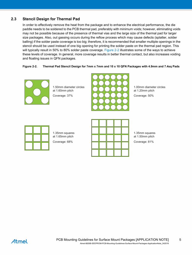
2.3 Stencil Design for Thermal Pad
In order to effectively remove the heat from the package and to enhance the electrical performance, the die
paddle needs to be soldered to the PCB thermal pad, preferably with minimum voids; however, eliminating voids
may not be possible because of the presence of thermal vias and the large size of the thermal pad for larger
size packages. Also, out gassing occurs during the reflow process which may cause defects (splatter, solder
balling) if the solder paste coverage is too big; therefore, it is recommended that smaller multiple openings in the
stencil should be used instead of one big opening for printing the solder paste on the thermal pad region. This
will typically result in 50% to 80% solder paste coverage. Figure 2-2 illustrates some of the ways to achieve
these levels of coverage. In general, more coverage results in better thermal contact, but also increases voiding
and floating issues in QFN packages.
Figure 2-2. Thermal Pad Stencil Design for 7mm x 7mm and 10 x 10 QFN Packages with 4.9mm and 7.4sq Pads
1.50mm diameter circlesat 1.60mm pitch
Coverage: 37%
1.35mm squaresat 1.65mm pitch
Coverage: 68%
1.00mm diameter circlesat 1.20mm pitch
Coverage: 50%
1.35mm squaresat 1.50mm pitch
Coverage: 81%
5PCB Mounting Guidelines for Surface Mount Packages [APPLICATION NOTE]Atmel-8826B-SEEPROM-PCB-Mounting-Guidelines-Surface-Mount-Packages-ApplicationNote_042016

3. Package Land Patterns
The following guidelines are derived form Mentor Graphics IPC LP Calculator. A full description of the board
recommendation, as well as, parts data that can be inserted into common PCB layout application is available
through Mentor Graphics.
3.1 SOIC
Figure 3-1. SOIC
Number of
Leads
Body Width
(Inches) Pitch C Y X
8 3.8 (0.150) 1.27 5.40 1.60 0.60
14 3.8 (0.150) 1.27 5.40 1.60 0.60
8 5.3 (0.208) 1.27 7.10 1.80 0.60
8 7.6 (0.300) 1.27 9.50 1.90 0.60
14 7.6 (0.300) 1.27 9.30 2.00 0.60
16 7.6 (0.300) 1.27 9.30 2.00 0.60
20 7.6 (0.300) 1.27 9.40 2.00 0.60
24 7.6 (0.300) 1.27 9.30 2.00 0.60
28 7.6 (0.300) 1.27 9.40 1.90 0.60
32 7.6 (0.300) 1.27 9.60 1.80 0.65
1
2
3
4
8
7
6
5
Y
X
C
PCB Mounting Guidelines for Surface Mount Packages [APPLICATION NOTE]Atmel-8826B-SEEPROM-PCB-Mounting-Guidelines-Surface-Mount-Packages-ApplicationNote_042016
6

3.2 TSSOP
Figure 3-2. TSSOP
Number of
Leads Body Pitch C Y X
8 3.00 x 3.00 0.65 4.40 1.45 0.45
8 4.40 x 3.00 0.65 5.80 1.45 0.45
14 4.40 x 5.00 0.65 5.80 1.45 0.45
16 4.40 x 5.00 0.65 5.90 1.50 0.45
20 4.40 x 6.50 0.65 5.80 1.50 0.45
24 4.40 x 7.80 0.65 5.90 1.50 0.45
28 4.40 x 7.80 0.50 5.80 1.50 0.30
28 4.40 x 9.70 0.65 5.80 1.45 0.45
28 6.00 x 9.70 0.65 7.50 1.50 0.45
44 4.40 x 11.30 0.50 5.80 1.50 0.30
Y
X
C
1
2
3
4
8
7
6
5
7PCB Mounting Guidelines for Surface Mount Packages [APPLICATION NOTE]Atmel-8826B-SEEPROM-PCB-Mounting-Guidelines-Surface-Mount-Packages-ApplicationNote_042016
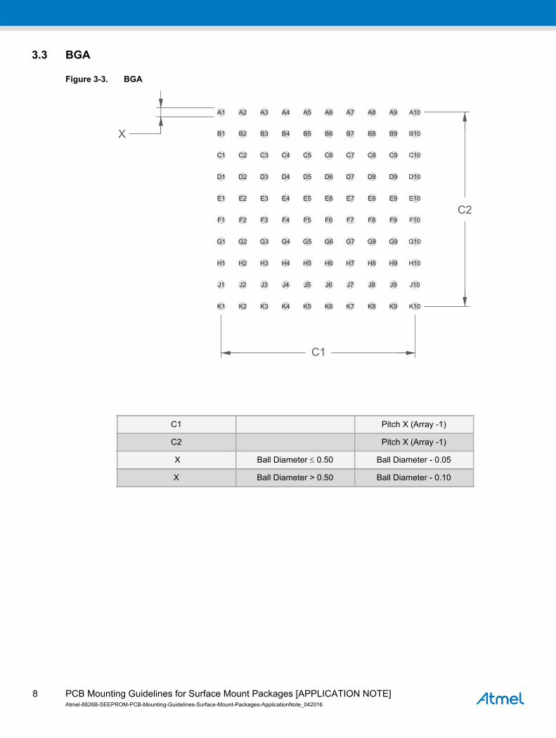
3.3 BGA
Figure 3-3. BGA
C1 Pitch X (Array -1)
C2 Pitch X (Array -1)
X Ball Diameter 0.50 Ball Diameter - 0.05
X Ball Diameter > 0.50 Ball Diameter - 0.10
X
C1
C2
A9A8A7A6A5A4A3A2A1 A10
C9C8C7C6C5C4C3C2C1 C10
D9D8D7D6D5D4D3D2D1 D10
E9E8E7E6E5E4E3E2E1 E10
F9F8F7F6F5F4F3F2F1 F10
G9G8G7G6G5G4G3G2G1 G10
H9H8H7H6H5H4H3H2H1 H10
J9J8J7J6J5J4J3J2J1 J10
B9B8B7B6B5B4B3B2B1 B10
K9K8K7K6K5K4K3K2K1 K10
PCB Mounting Guidelines for Surface Mount Packages [APPLICATION NOTE]Atmel-8826B-SEEPROM-PCB-Mounting-Guidelines-Surface-Mount-Packages-ApplicationNote_042016
8

3.4 WLCSP
Figure 3-4. WLCSP
C1 (X Pitch) X (Array -1)
C2 Y Pitch
X Ball Diameter = 0.25 0.24
X Ball Diameter = 0.30 0.30
X
C1
C2
A1
B1
C1
D1
A2
B2
C2
D2
9PCB Mounting Guidelines for Surface Mount Packages [APPLICATION NOTE]Atmel-8826B-SEEPROM-PCB-Mounting-Guidelines-Surface-Mount-Packages-ApplicationNote_042016

3.5 QFP
Figure 3-5. QFP
Number of
Leads Body Pitch
Form
Option C1 Y X C2
32 7 x 7 0.80 1.00 8.40 1.50 0.55 8.40
44 10 x 10 0.80 1.00 11.40 1.50 0.55 11.40
44 10 x 10 0.80 1.60 12.30 1.90 0.55 12.30
44 10 x 10 0.80 1.95 13.00 1.75 0.55 13.00
48 7 x 7 0.50 1.00 8.40 1.50 0.30 8.40
52 10 x 10 0.65 1.60 12.30 1.90 0.45 12.30
64 10 x 10 0.50 1.00 11.40 1.50 0.30 11.40
64 14 x 14 0.80 1.60 16.30 1.85 0.55 16.30
64 14 x 14 0.80 1.00 15.40 1.50 0.55 15.40
52 10 x 10 0.65 1.95 13.00 1.90 0.45 13.00
64 14 x 20 1.00 1.95 16.70 2.05 0.55 22.70
80 14 x 14 0.65 1.00 15.40 1.50 0.45 15.40
100 14 x 14 0.50 1.00 15.40 1.50 0.30 15.40
100 14 x 20 0.65 1.60 16.30 1.90 0.45 22.30
128 14 x 20 0.50 1.00 15.40 1.50 0.30 21.40
144 20 x 20 0.50 1.00 21.40 1.50 0.30 21.40
176 20 x 20 0.40 1.00 25.40 1.50 0.30 25.50
208 28 x 28 0.50 1.00 29.40 1.50 0.30 29.40
Y
X
C1
C2
12345678
2423222120191817
32 31 30 29 28 27 26 25
9 10 11 12 13 14 15 16
PCB Mounting Guidelines for Surface Mount Packages [APPLICATION NOTE]Atmel-8826B-SEEPROM-PCB-Mounting-Guidelines-Surface-Mount-Packages-ApplicationNote_042016
10
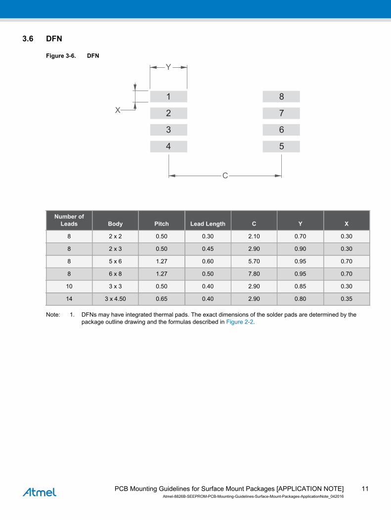
3.6 DFN
Figure 3-6. DFN
Note: 1. DFNs may have integrated thermal pads. The exact dimensions of the solder pads are determined by the
package outline drawing and the formulas described in Figure 2-2.
Number of
Leads Body Pitch Lead Length C Y X
8 2 x 2 0.50 0.30 2.10 0.70 0.30
8 2 x 3 0.50 0.45 2.90 0.90 0.30
8 5 x 6 1.27 0.60 5.70 0.95 0.70
8 6 x 8 1.27 0.50 7.80 0.95 0.70
10 3 x 3 0.50 0.40 2.90 0.85 0.30
14 3 x 4.50 0.65 0.40 2.90 0.80 0.35
Y
X
C
1
2
3
4
8
7
6
5
11PCB Mounting Guidelines for Surface Mount Packages [APPLICATION NOTE]Atmel-8826B-SEEPROM-PCB-Mounting-Guidelines-Surface-Mount-Packages-ApplicationNote_042016
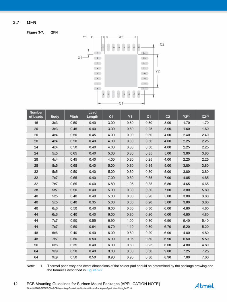
3.7 QFN
Figure 3-7. QFN
Note: 1. Thermal pads vary and exact dimensions of the solder pad should be determined by the package drawing and
the formulas described in Figure 2-2.
Number
of Leads Body Pitch
Lead
Length C1 Y1 X1 C2 Y2(1) X2(1)
16 3x3 0.50 0.40 3.00 0.80 0.30 3.00 1.70 1.70
20 3x3 0.45 0.40 3.00 0.80 0.25 3.00 1.60 1.60
20 4x4 0.50 0.45 4.00 0.90 0.30 4.00 2.40 2.40
20 4x4 0.50 0.40 4.00 0.80 0.30 4.00 2.25 2.25
24 4x4 0.50 0.40 4.00 0.80 0.30 4.00 2.25 2.25
24 5x5 0.65 0.40 5.00 0.80 0.35 5.00 3.80 3.80
28 4x4 0.45 0.40 4.00 0.80 0.25 4.00 2.25 2.25
28 5x5 0.65 0.40 5.00 0.80 0.35 5.00 3.80 3.80
32 5x5 0.50 0.40 5.00 0.80 0.30 5.00 3.80 3.80
32 7x7 0.65 0.40 7.00 0.80 0.35 7.00 4.85 4.85
32 7x7 0.65 0.60 6.80 1.05 0.35 6.80 4.65 4.65
38 5x7 0.50 0.40 5.00 0.80 0.30 7.00 3.80 5.80
40 5x5 0.40 0.40 5.00 0.80 0.20 5.00 3.80 3.80
40 5x5 0.40 0.35 5.00 0.80 0.20 5.00 3.80 3.80
40 6x6 0.50 0.40 6.00 0.80 0.30 6.00 4.80 4.80
44 6x6 0.40 0.40 6.00 0.80 0.20 6.00 4.80 4.80
44 7x7 0.50 0.55 6.90 1.00 0.30 6.90 5.40 5.40
44 7x7 0.50 0.64 6.70 1.10 0.30 6.70 5.20 5.20
48 6x6 0.40 0.40 6.00 0.80 0.20 6.00 4.80 4.80
48 7x7 0.50 0.50 6.90 0.95 0.30 6.90 5.50 5.50
56 6x6 0.35 0.40 6.00 0.80 0.25 6.00 4.80 4.80
64 9x9 0.50 0.40 9.00 0.80 0.30 9.00 7.25 7.25
64 9x9 0.50 0.50 8.90 0.95 0.30 8.90 7.00 7.00
X1
Y1 X2
C2
Y2
C1
32 31 30 26 25272829
9 10 11 15 16141312
2
3
4
5
6
7
1
8
23
22
21
20
19
18
24
17
PCB Mounting Guidelines for Surface Mount Packages [APPLICATION NOTE]Atmel-8826B-SEEPROM-PCB-Mounting-Guidelines-Surface-Mount-Packages-ApplicationNote_042016
12
3.7.1 PCB Design Guidelines for QFNs
The lands on QFN packages are rectangular in shape with rounded edges on the inside. Since the package
does not have any solder balls, the electrical connection between the package and the board is made by
printing the solder paste on the board and reflowing it after the component placement. In order to form reliable
solder joints, special attention is needed in designing the board pad pattern and the solder paste printing.
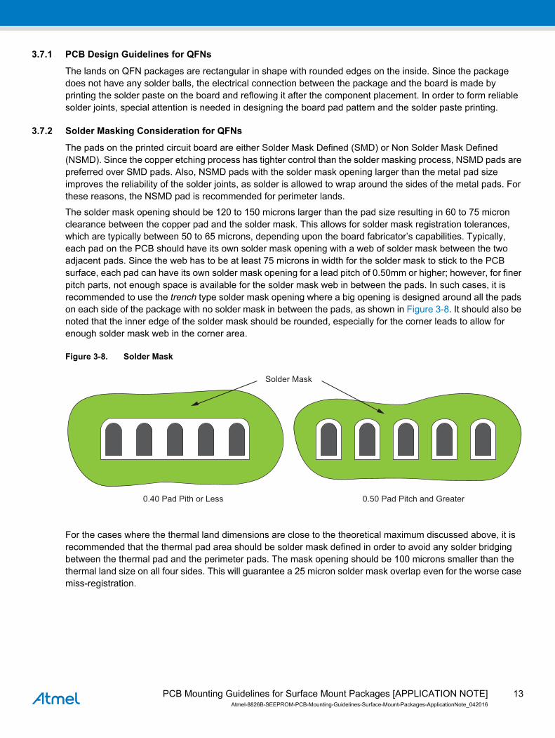
3.7.2 Solder Masking Consideration for QFNs
The pads on the printed circuit board are either Solder Mask Defined (SMD) or Non Solder Mask Defined
(NSMD). Since the copper etching process has tighter control than the solder masking process, NSMD pads are
preferred over SMD pads. Also, NSMD pads with the solder mask opening larger than the metal pad size
improves the reliability of the solder joints, as solder is allowed to wrap around the sides of the metal pads. For
these reasons, the NSMD pad is recommended for perimeter lands.
The solder mask opening should be 120 to 150 microns larger than the pad size resulting in 60 to 75 micron
clearance between the copper pad and the solder mask. This allows for solder mask registration tolerances,
which are typically between 50 to 65 microns, depending upon the board fabricator’s capabilities. Typically,
each pad on the PCB should have its own solder mask opening with a web of solder mask between the two
adjacent pads. Since the web has to be at least 75 microns in width for the solder mask to stick to the PCB
surface, each pad can have its own solder mask opening for a lead pitch of 0.50mm or higher; however, for finer
pitch parts, not enough space is available for the solder mask web in between the pads. In such cases, it is
recommended to use the trench type solder mask opening where a big opening is designed around all the pads
on each side of the package with no solder mask in between the pads, as shown in Figure 3-8. It should also be
noted that the inner edge of the solder mask should be rounded, especially for the corner leads to allow for
enough solder mask web in the corner area.
Figure 3-8. Solder Mask
For the cases where the thermal land dimensions are close to the theoretical maximum discussed above, it is
recommended that the thermal pad area should be solder mask defined in order to avoid any solder bridging
between the thermal pad and the perimeter pads. The mask opening should be 100 microns smaller than the
thermal land size on all four sides. This will guarantee a 25 micron solder mask overlap even for the worse case
miss-registration.
Solder Mask
0.40 Pad Pith or Less 0.50 Pad Pitch and Greater
13PCB Mounting Guidelines for Surface Mount Packages [APPLICATION NOTE]Atmel-8826B-SEEPROM-PCB-Mounting-Guidelines-Surface-Mount-Packages-ApplicationNote_042016

3.7.3 Board Mounting Guidelines for QFNs
Due to the small lead surface area and the sole reliance on the printed solder paste on the PCB surface, care
must be taken to form reliable solder joints for QFN packages. This is further complicated by the large thermal
pad underneath the package and its proximity to the inner edges of the leads. Although the pad pattern design
suggested above might help in eliminating some of the surface mounting problems, special considerations are
needed in the stencil design and the paste printing for both the perimeter and the thermal pads. Since the
surface mount process varies from company to company, careful process development is recommended. The
following sections provides some guidelines for the stencil design based on the experience of Atmel in the
surface mounting of QFN packages.
3.7.4 Stencil Design for Perimeter Pads for QFNs
Optimum and reliable solder joints on the perimeter pads should have about 50 to 75 microns (2 to 3 mils)
standoff height and a good side fillet on the outside. A joint with good stand-off height but no or low fillet will
have reduced life but may meet the application requirement. The first step in achieving good standoff is the
solder paste stencil design for the perimeter pads. The stencil aperture opening should be designed so
maximum paste release is achieved. This is typically accomplished by considering the following two ratios:
Area Ratio=Area of Aperture Opening / Aperture Wall Area
Aspect Ratio=Aperture width / Stencil Thickness
For rectangular aperture openings, as required for this package, these ratios are given as:
Area Ratio=LW / 2T(L+W)
Aspect Ratio=W / T
Where L and W are the aperture length and width, and T is stencil thickness.
For optimum paste release the area and the aspect ratios should be greater than 0.66 and 1.50 respectively. It
is recommended that the stencil aperture should be 1:1 to the PCB pad sizes as both the area and the aspect
ratio targets are easily achieved by this aperture. The opening can be reduced for a lead pullback option
because of the reduction of the solder able area on the package. The stencil should be laser cut and electro
polished. The polishing helps in smoothing the stencil walls which results in a better paste release. It is also
recommended that the stencil aperture tolerances should be tightly controlled, especially for 0.50mm pitch and
finer devices, as these tolerances can effectively reduce the aperture size.
3.7.5 Stencil Thickness and Solder Paste for QFNs
A stencil thickness of 0.125mm is recommended for 0.40mm and 0.50mm pitch parts. A laser-cut, stainless
steel stencil is recommended with electro-polished trapezoidal walls to improve the paste release. Since not
enough space is available underneath the part after reflow, it is recommended that the No Clean, Type 3 Paste
be used for mounting QFN packages. Nitrogen purge is also recommended during the reflow.
3.7.6 Solder Joint Standoff Height and Fillet Formation for QFNs
The solder joint standoff is a direct function of the amount of paste coverage on the thermal pad and the type of
vias used for QFNs with the exposed pad at the bottom. Board mounting studies sponsored by Amkor® have
clearly shown that the package standoff increases by increasing the paste coverage and by using plugged vias
in the thermal pad region. This is shown in Figure 3-9.
The standoff height varies by the amount of solder that wets or flows into the PTH via. The encroached via
provides an easy path for solder to flow into the PTH and decreases the package standoff height while the
plugged via impedes the flow of solder into the via due to the plugged vias closed barrel end. In addition, the
number of vias and their finished hole size will also influence the standoff height for encroached via design. The
standoff height is also affected by the paste type, the reactivity of the solder paste used during assembly, the
PCB thickness, the copper thickness, the surface finish, and the reflow profile.
PCB Mounting Guidelines for Surface Mount Packages [APPLICATION NOTE]Atmel-8826B-SEEPROM-PCB-Mounting-Guidelines-Surface-Mount-Packages-ApplicationNote_042016
14

To achieve 50 micron thick solder joints, which help in improving the board level reliability, it is recommended
the solder paste coverage be at least 50% for the plugged vias and 75% for the encroached via types.
The peripheral solder joint fillets formation is also driven by multiple factors. It should be realized that only the
bottom surface of the leads are plated with solder and not the ends. The bare Cu on the side of the leads may
oxidize if the packages are stored in an uncontrolled environment. It is possible that a solder fillet will be formed
depending on the solder paste (flux) used and the level of oxidation.
Figure 3-9. Graph and Data Source — Amkor Technologies Application Notes for Surface Mount Assembly of
Amkor’s MicroLeadFrame® (MLF®) Packages
The fillet formation is also a function of the PCB land size, the printed solder volume, and the package standoff
height. Since there is only limited solder available, higher standoff (controlled by the paste coverage on the
thermal pad) may not leave enough solder for fillet formation. Conversely, if the standoff is too low, large convex
shape fillets may form. Since center pad coverage and via type were shown to have the greatest impact on the
standoff height, the volume of solder necessary to create optimum fillet varies. The package standoff height and
the PCB pads size will establish the required volume.
Standoff Height as a Function of Via Type & Center Pad Solder Paste Coverage3.25
3.00
2.75
2.50
2.25
2.00
1.75
1.50
1.25
1.00
0.75
0.50
0.25
0Plugged
Via @ 37%Paste
Coverage48 IO
EncroachVia @ 67%
PasteCoverage
48 IO
EncroachVia @ 37%
PasteCoverage
48 IO
PluggedVia @ 67%
PasteCoverage
48 IO
PluggedVia @ 50%
PasteCoverage
68 IO
EncroachVia @ 81%
PasteCoverage
68 IO
EncroachVia @ 50%
PasteCoverage
68 IO
PluggedVia @ 81%
PasteCoverage
68 IO
StandoffHeight(mils)
15PCB Mounting Guidelines for Surface Mount Packages [APPLICATION NOTE]Atmel-8826B-SEEPROM-PCB-Mounting-Guidelines-Surface-Mount-Packages-ApplicationNote_042016

3.7.7 Reflow Profile for QFNs
The reflow profile and the peak temperature have a strong influence on void formation. Amkor has conducted
experiments with the different reflow profiles (ramp-to-peak vs. ramp-hold-ramp), the peak reflow temperatures,
and the times above liquidus using Alpha Metal’s UP78 solder paste. Some of the representative profiles are
shown in Figure 3-9. Generally, it is found that the 37% paste coverage, plugged via, voids in the thermal pad
region for the plugged vias reduce as the peak reflow temperature is increased from 210C to 215 – 220C. For
the encroached vias, it is found that the solder extrusion from the bottom side of the board reduces as the reflow
temperature is reduced.
3.7.8 Rework Guidelines for QFNs
Since solder joints are not fully exposed in the case of QFNs, any retouch is limited to the side fillet. For defects
underneath the package, the whole package has to be removed. Rework of the QFN packages can be a
challenge due to their small size. In most applications, the QFNs will be mounted on smaller, thinner, and
denser PCBs that introduce further challenges due to the handling and the heating issues. Since reflow of the
adjacent parts is not desirable during rework, the proximity of other components may further complicate this
process. Because of the product dependent complexities, the following only provides a guideline and a starting
point for the development of a successful rework process for these packages.
The rework process involves the following steps:
1. Component removal
2. Site redress
3. Solder paste application
4. Component placement
5. Component attachment
These steps are discussed more in detail in the following sections. Prior to any rework, it is strongly
recommended that the PCB assembly be baked for at least four hours at 125C to remove any residual moisture
from the assembly.
3.7.9 Component Removal for QFNs
The first step in removal of the component is the reflow of the solder joints attaching the component to the
board. Ideally, the reflow profile for the part removal should be the same as the one used for the part
attachment; however, the time above liquidus can be reduced as long as the reflow is complete.
In the removal process, it is recommended that the board should be heated from the bottom side using
convective heaters and hot gas or air should be used on the top side of the component. Special nozzles should
be used to direct the heating in the component area and the heating of adjacent components should be
minimized. Excessive airflow should also be avoided since this may cause the package to skew. Air velocity of
15-20 liters per minute is a good starting point.
Once the joints have reflowed, the vacuum lift-off should be automatically engaged during the transition from the
reflow to cool down. Because of their small size the vacuum pressure should be kept below 15 inches of Hg.
This will allow the component not to be lifted off if all joints have not been reflowed and avoid pad damage.
3.7.10 Site Redress for QFNs
After the component has been removed, the site needs to be cleaned properly. It is best to use a combination of
a blade-style conductive tool and a desoldering braid. The width of the blade should be matched to the
maximum width of the footprint and the blade temperature should be low enough not to cause any damage to
the circuit board. Once the residual solder has been removed, the lands should be cleaned with a solvent. The
solvent is usually specific to the type of paste used in the original assembly and the paste manufacturer’s
recommendations should be followed.
PCB Mounting Guidelines for Surface Mount Packages [APPLICATION NOTE]Atmel-8826B-SEEPROM-PCB-Mounting-Guidelines-Surface-Mount-Packages-ApplicationNote_042016
16

3.7.11 Solder Paste Printing for QFNs
Because of their small size and the fine pitches, solder paste deposition for the QFNs requires extra care;
however, a uniform and precise deposition can be achieved if a miniature stencil specific to the component is
used. The stencil aperture should be aligned with the pads under 50X to 100X magnification. The stencil should
then be lowered onto the PCB and the paste should be deposited with a small metal squeegee blade.
Alternatively, the mini stencil can be used to print paste on the package side. A 125 microns thick stencil with
the aperture size and shape same as the package land should be used. Also, no-clean flux should be used, as
small standoff of the QFNs does not leave much room for cleaning.
3.7.12 Component Placement for QFNs
QFN packages are expected to have superior self-centering ability due to their small mass and the placement of
this package should be similar to that of BGAs. As the leads are on the underside of the package, a split-beam
optical system should be used to align the component on the board. This will form an image of leads overlaid on
the mating footprint and aid in proper alignment. Again, the alignment should be done at 50X to 100X
magnification. The placement machine should have the capability of allowing fine adjustments in the X, Y, and
the rotational axes.
3.7.13 Component Attachment for QFNs
The reflow profile developed during original attachment or removal should be used to attach the new
component. Since all reflow profile parameters have already been optimized, using the same profile will
eliminate the need for thermocouple feedback and will reduce operator dependencies.
3.7.14 Summary
Successful use of the AT88RF1354 QFN package requires careful development of the PCB and the
manufacturing process. This document contains guidelines to assist the design and manufacturing engineers in
optimizing the PC board and processes. These guidelines include:
PCB thermal pad sized to match the package thermal pad
1oz copper thickness on all layers for optimum heat transfer
Nine or more thermal vias in the PCB thermal pad for heat transfer
SMD solder masking of thermal pad
NSMD solder masking of pads for package pins
50 to 75 micron solder joint standoff height
Laser-cut, electro-polished 0.125mm stainless steel stencil
No Clean, Type 3 solder paste
Hot gas rework process
4. Disclaimer
These are only general guidelines Atmel received from its package vendor. Atmel does not make direct
recommendation for board design nor does it take legal liability and responsibility for the information in this
document. Please refer to the IPC website for more information regarding board design and processing.
5. References
1. Application Notes for Surface Mount Assembly of Amkor’s MicroLeadFrame (MLF) packages.
2. Mentor Graphics IPC-7351 Calculator.
3. IPC -9502.
17PCB Mounting Guidelines for Surface Mount Packages [APPLICATION NOTE]Atmel-8826B-SEEPROM-PCB-Mounting-Guidelines-Surface-Mount-Packages-ApplicationNote_042016
6. Revision History
Function
Doc. Rev. Date Comments
8826B 04/2016 Updated DFN table, page dimensions, and disclaimer page.
8826A 03/2013 Initial document release.
PCB Mounting Guidelines for Surface Mount Packages [APPLICATION NOTE]Atmel-8826B-SEEPROM-PCB-Mounting-Guidelines-Surface-Mount-Packages-ApplicationNote_042016
18

XX X XX X
Atmel Corporation 1600 Technology Drive, San Jose, CA 95110 USA T: (+1)(408) 441.0311 F: (+1)(408) 436.4200 | www.atmel.com
© 2016 Atmel Corporation. / Rev.: Atmel-8826B-SEEPROM-PCB-Mounting-Guidelines-Surface-Mount-Packages-ApplicationNote_042016.
Atmel®, Atmel logo and combinations thereof, Enabling Unlimited Possibilities®, and others are registered trademarks or trademarks of Atmel Corporation in U.S. and other countries. Other terms and product names may be trademarks of others.
DISCLAIMER: The information in this document is provided in connection with Atmel products. No license, express or implied, by estoppel or otherwise, to any intellectual property rightis granted by this document or in connection with the sale of Atmel products. EXCEPT AS SET FORTH IN THE ATMEL TERMS AND CONDITIONS OF SALES LOCATED ON THEATMEL WEBSITE, ATMEL ASSUMES NO LIABILITY WHATSOEVER AND DISCLAIMS ANY EXPRESS, IMPLIED OR STATUTORY WARRANTY RELATING TO ITS PRODUCTSINCLUDING, BUT NOT LIMITED TO, THE IMPLIED WARRANTY OF MERCHANTABILITY, FITNESS FOR A PARTICULAR PURPOSE, OR NON-INFRINGEMENT. IN NO EVENTSHALL ATMEL BE LIABLE FOR ANY DIRECT, INDIRECT, CONSEQUENTIAL, PUNITIVE, SPECIAL OR INCIDENTAL DAMAGES (INCLUDING, WITHOUT LIMITATION, DAMAGESFOR LOSS AND PROFITS, BUSINESS INTERRUPTION, OR LOSS OF INFORMATION) ARISING OUT OF THE USE OR INABILITY TO USE THIS DOCUMENT, EVEN IF ATMEL HASBEEN ADVISED OF THE POSSIBILITY OF SUCH DAMAGES. Atmel makes no representations or warranties with respect to the accuracy or completeness of the contents of thisdocument and reserves the right to make changes to specifications and products descriptions at any time without notice. Atmel does not make any commitment to update the informationcontained herein. Unless specifically provided otherwise, Atmel products are not suitable for, and shall not be used in, automotive applications. Atmel products are not intended,authorized, or warranted for use as components in applications intended to support or sustain life.
SAFETY-CRITICAL, MILITARY, AND AUTOMOTIVE APPLICATIONS DISCLAIMER: Atmel products are not designed for and will not be used in connection with any applications wherethe failure of such products would reasonably be expected to result in significant personal injury or death (“Safety-Critical Applications”) without an Atmel officer's specific writtenconsent. Safety-Critical Applications include, without limitation, life support devices and systems, equipment or systems for the operation of nuclear facilities and weapons systems.Atmel products are not designed nor intended for use in military or aerospace applications or environments unless specifically designated by Atmel as military-grade. Atmel products arenot designed nor intended for use in automotive applications unless specifically designated by Atmel as automotive-grade.
![Nexperia...[3] Device mounted on an FR4 PCB, single-sided copper , tin-plated and mounting pad for collector 6 cm 2. [4] Device mounted on an FR4 PCB, 4-layer copper, tin-plated and](https://static.fdocuments.us/doc/165x107/6080bfbeb565e62c6b5e7711/nexperia-3-device-mounted-on-an-fr4-pcb-single-sided-copper-tin-plated.jpg)