
Pb-Free Reflow, PCB Degradation, and the Influence of Moisture Absorption
39
Kerin O’Toole, Bob Esser, Seth Binfield, Craig Hillman, Cheryl Tulkoff and Joe Beers DfR Solutions / Gold Circuits Pb-Free Reflow, PCB Degradation, and the Influence of Moisture Absorption
-
Upload
cheryl-tulkoff -
Category
Technology
-
view
141 -
download
2
description
Increasing number of companies reporting cracking and delamination of printed circuit boards –Predominantly under Pb-free reflow but some under SnPb reflow conditions Several telecom and enterprise OEMs are reporting PCB robustness is their primary concern regarding Pb-free reliability Cracking or delamination during reflow is a stress vs. strength phenomenon –Either the environmental stress was higher than expected or the material strength was lower than expected
Transcript of Pb-Free Reflow, PCB Degradation, and the Influence of Moisture Absorption

Kerin O’Toole, Bob Esser, Seth Binfield, Craig Hillman, Cheryl Tulkoff and Joe Beers
DfR Solutions / Gold Circuits
Pb-Free Reflow, PCB Degradation, and
the Influence of Moisture Absorption

Introduction
• An increasing number of clients of DfR Solutions are reporting cracking and delamination of printed circuit boards – Predominantly under Pb-free reflow but some under SnPb reflow
conditions
• Several telecom and enterprise OEMs are reporting PCB robustness is their primary concern regarding Pb-free reliability
• Cracking or delamination during reflow is a stress vs. strength phenomenon – Either the environmental stress was higher than expected or the
material strength was lower than expected

Research Study
• An earlier customer case study showed: – Initial reduction in PCB cracking / delam after baking
for 48 hours at 125C • Could suggest de-absorption of moisture
• May also suggest sublimation of volatiles or a cure process that is improving adhesion
– Final elimination of cracking / delam after baking for 48 hours at 125C and reducing maximum reflow temperature to 245C
• To better assess the root cause of delamination of printed circuit boards, an internal study on the influence of moisture absorption was initiated.

Coupon Design
• Two coupon designs (Standard / Advanced) – Each coupon design has three sections and six test structures
• Section 1: ‘Shield over shield’ (Test Structure A) – Plane-to-plane spacing: See slide 4 (same for both standard
and advanced designs)
• Section 2: PTH with internal planes (Test Structures B and C)
– Plane-to-plane spacing: See slide 4 (same for both standard and advanced designs)
– Drill diameter: Standard: 15 mil; Advanced: 12 mil
– Clearance: Standard: Drill + 10 mil; Advanced: Drill + 7 mil
– Pitch: 78 mil (same for both standard and advanced)
– Pad diameter: 27 mil
• Section 3: PTH with no internal planes (Test Structures D, E, & F)
– Drill diameter: Standard: 15 mil; Advanced: 12 mil
– Pitch: Standard: 40 mil; Advanced: 32 mil
– Pad diameter: 27 mil

Coupon Stackup
• Board thickness
– 150 mil (3.75 mm)
• Number of layers
– 26
• Dielectric thickness
– 3 mil (75 mm), 4 mil (100 mm), and 5 mil (125 mm)
• Glass fabric
– 106, 1080, 7628, and 2116
• Copper foil thickness
– 0.5 oz (17.5 mm), 1 oz (35 mm), and 2 oz (70 mm)
1 0.65 foil 1/2 oz
3 prepreg 1 x 1080
2 0.65 1 oz
4 core
3 0.65 1 oz
14 prepreg 2 x 7628
4 0.65 1/2 oz
4 core
5 0.65 1/2 oz
5 prepreg 2 x 1080
6 2.4 2 oz
4 core 2 x 10⁶
7 2.4 2oz
5 prepreg 1080 + 2116
8 0.65 1/2 oz
5 core 1 x 2116 HR
9 0.65 1/2 oz
3 prepreg 1 x 1080
10 1.4 1 oz
4 core 2 x 10⁶
11 1.4 1 oz
3 prepreg 1 x 1080
12 0.65 1/2 oz
5 core 1 x 2116 HR
13 0.65 1/2 oz
5 prepreg 1080 + 2116
14 0.65 1/2 oz
5 core 1 x 2116 HR
15 0.65 1/2 oz
3 prepreg 1 x 1080
16 1.4 1 oz
4 core 2 x 10⁶
17 1.4 1 oz
3 prepreg 1 x 1080
18 0.65 1/2 oz
5 core 1 x 2116 HR
19 0.65 1/2 oz
5 prepreg 1080 + 2116
20 2.4 2 oz
4 core 2 x 10⁶
21 2.4 2oz
5 prepreg 2 x 1080
22 0.65 1/2 oz
4 core
23 0.65 1/2 oz
14 prepreg 2 x 7628
24 0.54 1 oz
4 core
25 0.65 1 oz
3 prepreg 1 x 1080
26 0.65 foil 1/2 oz

Test Structures
• The current design had 6 test structures (A-F), with multiple nets per
test structure
• Test Structure A: shield over shield (copper planes with no PTHs)
– Alternating planes are tied to power (node A1) and ground (node A2)
• Test Structure B: shield over shield (copper planes with PTHs)
– Non-functional pads on every layer
– Alternating planes are tied to power1 (node B1) and ground (node B2)
– PTHs are daisy chained and are tied to power2 (node V1)
• Test Structure C: shield over shield (copper planes with PTHs)
– Non-functional pads on every other layer
– Alternating planes are tied to power1 (node C1) and ground (node C2)
– PTHs are daisy chained and are tied to power2 (node V5)

Test Structures B and C (Example)
• Test structures B (top)
and C (bottom)
– Layer 19 (left)
– Layer 20 (right)
• Note how non-
functional pads are
present in both layers
for test structure B, but
are absent in layer 19
for test structure C

Nets
• Nets A1-A2, B1-B2, and C1-C2 allow
measurement of capacitance between
layers
• Nets V1-B1, V1-B2, V5-C1, and V5-C2
allow measurement of capacitance
between PTHs and layers

Coupon Material
• Manufacturer: ITEQ – Product: IT-180
– High Tg phenolic resin
• Material characteristics – Glass transition temperature (Tg): 180oC +/- 5oC (DSC) [1]
– Decomposition temperature (Td): 350oC +/- 5% (TMA) [2]
– No available data on time to delamination
• Astec Power reported that ITEQ IT-180 survived 4 reflow cycles (245oC peak) at MSL3, MSL4, and MSL5 [3] – Testing ceased after 4 reflow cycles.
[1] http://www.iteq.com.cn/product.html
[2] “2006 status & 2007 outlook.” Global SMT & Packaging, January 2007. <http://www.trafalgar2.com/documents/Columns-Custer/7.1-custer.pdf>.
[3] John Kippen. “A Test Coupon Approach to Qualification of Lead-Free PCB Laminates for DC/DC Converters.” DCDC Technical White Paper from Astec Power,
December 2004. <http://www.astecpower.com/whitepaper/dcdc/Done%20A%20WP-Test%20Coupon%20Approach%20to%20Qualification%20of%20Lead.pdf>.

Phase 1: Simulated Reflow
• 260oC reflow, test 1: – 5 advanced coupons*
– 30 reflow cycles at 260oC peak
– Monitored shield over shield capacitance (test structure A) out of package and after each reflow cycle
– All capacitance measurements taken at room temperature (26oC +/-2oC.)
• 280oC reflow: – 5 advanced coupons*
– 12-13 reflow cycles at 280oC peak
– Monitored shield over shield capacitance (test structure A) out of package and after each reflow cycle
– All capacitance measurements taken at room temperature (26oC +/-2oC.)
* Note: standard and advanced designs are identical for test structure A (shield-over-shield)

Phase 1: Simulated Reflow, Part 2
• 260oC reflow, test 2: – 5 standard coupons
– 15 reflow cycles at 260oC peak
– Monitored shield over shield capacitance (test structures A, B, and C) out of package and after each reflow cycle
– Monitored shield-PTH capacitance (test structures B and C) out of package and after each reflow cycle
– All capacitance measurements were taken at room temperature (26oC +/-2oC)

Phase 2: Moisture Sensitivity
• Protocol:
– 3 boards per condition
– 3 conditions: MSL1, MSL2, and MSL2a
– Boards were dried at 125oC for 72 to 88 hours immediately
before humidity testing
– Humidity testing protocol followed the standards outlined in
J-STD-020C
– All boards were subjected to 3 reflow cycles, starting 15
minutes after removal from humidity chamber
– Monitored weight gain and capacitance throughout the
testing periods
Note: GCE noted concerns with long-term
exposure to elevated temperature inducing
degradation. Future pre-bakes may need to be
performed at lower temperatures (~105C)

Phase 2: Moisture Sensitivity
• Protocol continued:
– MSL 1:
• 88-hour prebake at 125oC
• 85oC/85%RH, 168 hours
• Monitored weight gain and shield-shield capacitance on test structure A
– MSL 2:
• 88-hour prebake at 125oC
• 85oC/60%RH, 168 hours
• Monitored weight gain and shield-shield capacitance on test structure A
– MSL 2a:
• 72-hour prebake at 125oC
• 60oC/60%RH, 120 hours
• Monitored weight gain and shield-shield capacitance on test structures A-C,
as well as shield-PTH capacitance on test structures B and C

Phase 1: 260oC Reflow Results, Test 1
Normalized Capacitance vs. Number of Reflows,
260oC Peak
0.98
0.99
1
0 5 10 15 20 25 30
Reflows (#)
Ca
pa
cit
an
ce
(n
orm
alize
d)
Shield over Shield Coupon (A)
180 Tg Phenolic Material
Degradation occurs after ? reflows at 260C
Average slope: -0.00055
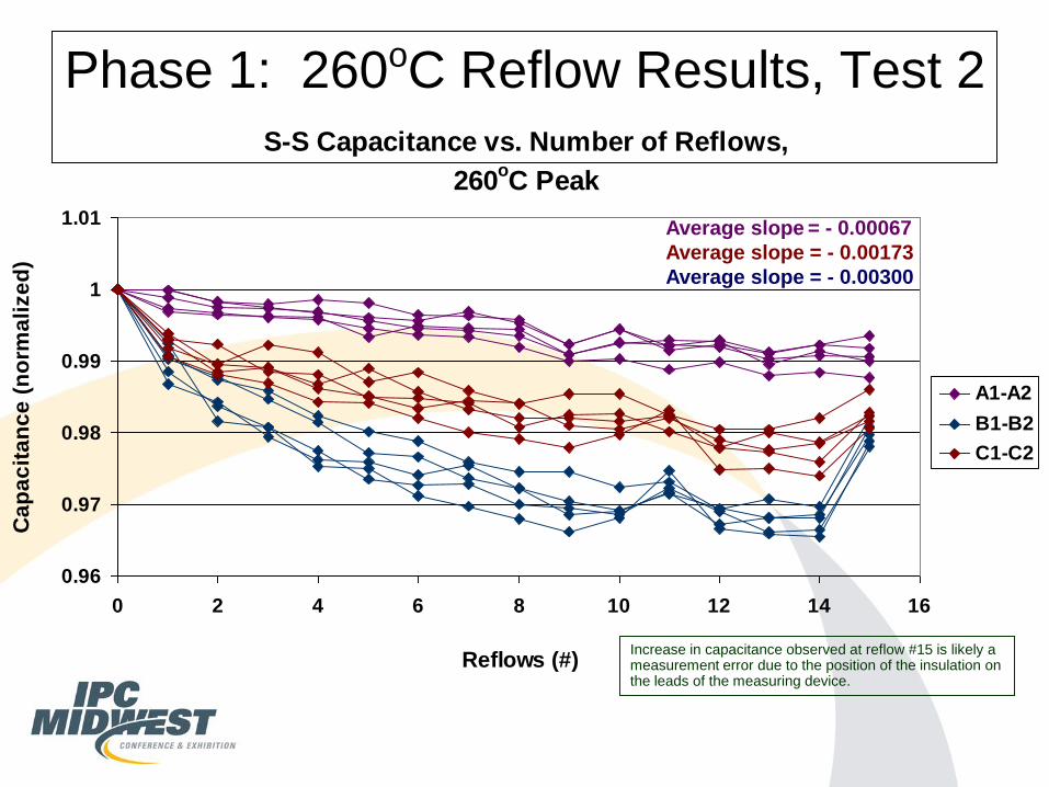
Phase 1: 260oC Reflow Results, Test 2
S-S Capacitance vs. Number of Reflows,
260oC Peak
0.96
0.97
0.98
0.99
1
1.01
0 2 4 6 8 10 12 14 16
Reflows (#)
Ca
pa
cit
an
ce
(n
orm
ali
ze
d)
A1-A2
B1-B2
C1-C2
Increase in capacitance observed at reflow #15 is likely a measurement error due to the position of the insulation on the leads of the measuring device.
Average slope = - 0.00067
Average slope = - 0.00173
Average slope = - 0.00300

Phase 1: 260oC Reflow Results, Test 2 S-PTH Capacitance vs. Number of Reflows,
260C Peak
0.86
0.88
0.9
0.92
0.94
0.96
0.98
1
1.02
0 2 4 6 8 10 12 14 16
Reflows (#)
Ca
pa
cit
an
ce
(n
orm
ali
ze
d)
V1-B2
V1-B1
V5-C2
V5-C1same board
Some organizations believe a 10% or
greater drop in capacitance is indicative of
cracking or delamination

Phase 1: 280oC Reflow Results Normalized Capacitance vs. Number of Reflows,
280oC Peak
0.98
0.99
1.00
0 1 2 3 4 5 6 7 8 9 10 11 12 13 14
Reflows (#)
Ca
pa
cit
an
ce
(n
orm
alize
d)
Shield over Shield Coupon (A)
180 Tg Phenolic Material
Degradation occurs after 4 reflows at 280C
Average slope: -0.00076

Phase 1: Shield over Shield Observations
• Steady decrease in shield over shield (S-S) capacitance at 260ºC, but no clear roll-off point
• Test structures A, B, and C degrade at different rates, with B showing the greatest change in capacitance
– Test structure B has an average degradation rate almost 5X greater than that of test structure A
– Test structure C has an average degradation rate almost 3X greater than that of test structure A
• 280ºC samples show a stronger (~0.5% average) decrease in shield over shield capacitance after 4 reflows, but gradual degradation continues with each subsequent reflow cycle
– Average degradation rate of the 280ºC samples was approximately 50% greater that of the 260ºC samples

Phase 1: Shield - PTH Observations
• Shield to PTH (S-PTH) capacitance: – A higher degree of degradation compared to shield
over shield
• After just one reflow cycle, the degradation in S-PTH capacitance is comparable to that of the S-S capacitance after 15 reflow cycles.
– Very significant decrease in capacitance after 4 reflow cycles, followed by very gradual degradation with an extensive degree of variation
– One board had a much larger decrease in capacitance on all S-PTH nets

Phase 1, Part 1: Cross Section
• Cross section of sample after 33 reflows at 260oC peak
• Low magnification: no cracking observed

Phase 2: Moisture Absorption Results Moisture Absorption vs. Time
0.00%
0.05%
0.10%
0.15%
0.20%
0.25%
0.30%
0.35%
0.40%
0.45%
0.50%
0 20 40 60 80 100 120 140 160 180
Time (hours)
Weig
ht
(%)
85oC / 85%RH
85oC / 60%RH
60oC / 60%RH

Phase 2: Moisture Absorption Results Average Moisture Absorption vs. Time
y = 0.0003x + 0.0003
y = 0.0002x + 0.0001
y = 0.0002x + 0.0003
0.00%
0.05%
0.10%
0.15%
0.20%
0.25%
0.30%
0.35%
0.40%
0.45%
0.50%
0 2 4 6 8 10 12 14
Time (sqrt(hr))
Weig
ht
(%)
85C/85%RH
85C/60%RH
60C/60%RH

Phase 2: Moisture Absorption Observations
• The 85oC/85%RH samples showed the largest weight gain due to moisture absorption
• The 60oC/60%RH samples showed the smallest weight gain due to moisture absorption
• Higher temperature results in increased moisture absorption at 60%RH
• Moisture absorption is proportional to the square root of time in hours, as per Fick’s law of diffusion
– Deviation is observed as moisture saturation is approached
– Saturation seems to initiate around 64 (82) hours

Phase 2: Moisture Capacitance Results S-S Capacitance vs. Weight Gain
0.99
1.00
1.01
1.02
1.03
1.04
1.05
1.06
1.07
0.00% 0.10% 0.20% 0.30% 0.40% 0.50%
Moisture Absorption
Cap
acit
an
ce (
no
rmalized
)
85/85, A1-A2
85/60, A1-A2
60/60, A1-A2
60/60, B1-B2
60/60, C1-C2

Phase 2: Moisture Sensitivity Results S-PTH Capacitance vs. Weight Gain,
60C/60%RH
0.99
1
1.01
1.02
1.03
1.04
1.05
1.06
1.07
0.00% 0.05% 0.10% 0.15% 0.20% 0.25%
Moisture Absorption
Cap
acit
an
ce (
no
rmali
zed
)
V1-B2
V1-B1
V5-C2
V5-C1

Phase 2: Moisture Capacitance
Observations
• Capacitance as a function of moisture absorption shows similar trends for all three environmental conditions
• Shield-over-shield with no PTHs showed minimal change up to 0.15%, followed by approximately linear behavior
• The shield-over-shield with PTHs showed a larger increase in capacitance relative to the amount of moisture absorbed
• Shield-to-PTH capacitance showed a larger increase in capacitance relative to amount of moisture absorbed, but no clear trend

Phase 2: Moisture Sensitivity Reflow Results
S-S Capacitance vs. Number of Reflows
0.92
0.93
0.94
0.95
0.96
0.97
0.98
0.99
1
1.01
0 1 2 3
Reflows (#)
Cap
acit
an
ce (
no
rmali
zed
)
85/85, A1-A2
85/60, A1-A2
60/60, A1-A2
85/85, B1-B2
85/60, B1-B2
60/60, B1-B2
85/85, C1-C2
85/60, C1-C2
60/60, C1-C2

Phase 2: Moisture Sensitivity Reflow Results
S-PTH Capacitance vs. Number of Reflows
0.92
0.93
0.94
0.95
0.96
0.97
0.98
0.99
1
1.01
0 1 2 3
Reflows (#)
Cap
acit
an
ce (
no
rmali
zed
)
85/85, V1-B2
85/60, V1-B2
60/60, V1-B2
85/85, V1-B1
85/60, V1-B1
60/60, V1-B1
85/85, V5-C2
85/60, V5-C2
60/60, V5-C2
85/85, V5-C1
85/60, V5-C1
60/60, V5-C1

Phase 2: Moisture Sensitivity (S-S Results)
• Capacitance degradation – Test structure B degrades more than test structure C, which
degrades more than test structure A
• Same as reflow without moisture preconditioning
– 60ºC/60%RH degrades the least, while 85ºC/60%RH and 85ºC/85%RH seem to show similar behavior
• Was capacitance degradation due to moisture desorption or damage accumulation within the coupon? – After 85ºC/85%RH, 4% increase in capacitance
– After 3 reflows, 4% decrease in capacitance
– Is there moisture remaining after the first reflow?

Phase 2: Moisture Sensitivity (S-PTH Results)
• S-PTH degrades more than S-S – Maximum 6% reduction vs. maximum 4%
reduction
• 60ºC/60%RH degrades less than the other two conditions
• Test structure B generally degrades more than test structure C

Delamination
• Delamination occurred primarily in featureless areas
• Evidence of failures only in specimens tested as per
MSL1 (85oC/85%RH, 168 hours)
– These samples had the highest % weight gain
• No visible delamination in MSL2 (85oC/60%RH, 168
hours) and MSL2a (60oC/60%RH, 120 hours) samples
• No observable delamination in any “dry samples” from
phase 1

Phase 2: Moisture Sensitivity Results
Delamination observed in 85oC/85%RH test boards
2.5X side view of 85oC/85%RH board after 3 reflows at 260oC peak
delamination
solder mask

Coupons after 85C/85%RH + 3 Reflows
Top Bottom
Red arrows mark internal delamination

Phase 1: Observations
• Variation in degradation rates on different
test structures may be evidence of
microcracking in the PCB
– Microcracking seems to be exacerbated by
the presence of PTHs
– Microcracking also seems to be exacerbated
by the presence of non-functional pads

Phase 1 (cont.)
• One board had a significant decrease in capacitance on all S-PTH nets – On two supposedly isolated test structures (B and C)
• Potential root-cause (#1): Measurement error due to measurement at elevated temperature – Unlikely because ‘normal’ S-S measurements were taken at the
same time as the anomalous S-PTH measurements
• Potential root-cause (#2): Possibility of a plane-PTH short – Unlikely to affect both test structures B and C
• Potential root-cause (#3): Extensive microcracking – A similar decrease in S-S capacitance was not observed

Phase 2
• The 85ºC/60%RH seem to show a larger
increase in capacitance for a given amount of
moisture absorption
– Uncertain as to the driver for this behavior
• Shield-over-shield test structures with PTHs
showed a greater increase in capacitance for a
given amount of moisture absorption
– Damages caused during drilling could enable more
localized moisture absorption (tiny cracks or
delamination can absorb more water)

Phase 2 (cont.)
• Shield-PTH capacitance vs. moisture absorption:
– No clear trend
– For the same level of moisture absorption, test
structure B generally showed a larger increase in
capacitance than test structure C
– Test structure B then displayed a larger degradation
in capacitance than test structure C after reflow

Phase 1 vs. Phase 2 Observations
• Moisture sensitivity samples display more
extensive degradation after reflow
– 260ºC samples from phase 1 show approximately 1%
degradation in test structure A after 15 reflows
– Phase 2 samples show an average of nearly 1%
degradation for all conditions on test structure A after
3 reflows
– This trend holds true for all S-S and S-PTH nets

Conclusions
• Measurable change of capacitance after each reflow
– Discrimination between different test structures and MSL
exposures strongly suggests approach captures material
degradation, as opposed to an increase in resistance at contact
pads due to oxidation
– However, contact resistance should be quantified in next round
of testing through ESR measurements
• Strong difference in shield-over-shield capacitance
between test structures B and C, due to the presence of
non-functional pads, is very interesting and should be
further characterized
– Future focus on clearance and pad dimensions