
Parametric Amplifiers and Upconverters - Tuks · C¸ FOREWORD This report is an expanded version of...
49
r ... NRL Report 6024 Parametric Amplifiers and Upconverters ALAN C. MACPHERSON Solid State Electronics Branch Electronics Division May 5, 1964 U.S. NAVAL RESEARCH LABORATORY Washington, D.C.
Transcript of Parametric Amplifiers and Upconverters - Tuks · C¸ FOREWORD This report is an expanded version of...

r ...
NRL Report 6024
Parametric Amplifiers and Upconverters
ALAN C. MACPHERSON
Solid State Electronics BranchElectronics Division
May 5, 1964
U.S. NAVAL RESEARCH LABORATORYWashington, D.C.
CONTENTS
ForewordAbstract ivProblem Status ivAuthorization iv
INTRODUCTION 1
Nomenclature 1History 2
NOISE 2
Introduction 2How Noise is Described 3Circuit Calculations 4Noise Figure 5System Sensitivity 7Tandem Connection of Two-Port Networks 9
QUALITATIVE DESCRIPTION OF PARAMETRIC AMPLIFICATION 10
PARAMETRIC OR VARACTOR DIODES 13
GENERAL THEORY OF SMALL SIGNAL NONLINEAR CAPACITANCE 14
Introduction 14Mixing in the Nonlinear Capacitance 15Various Operating Modes 17Properties of the Three-Port Nonlinear Capacitance Mixer 18
THE UPCONVERTER 20
The Circuit Equations 20Input and Output Conductance 20Gain 21Equivalent Circuit 21Noise Figure 22Bandwidth 22
PROPERTIES OF NEGATIVE RESISTANCE AMPLIFIERS 22
Introduction 22Transducer Gain and Stability 23Available Gain and Noise Figure 24Overall Noise Figure 25
THE NEGATIVE RESISTANCE PARAMETRIC AMPLIFIER 26
Circuit Equations 26Conductance Calculations 26
i
Noise in the Negative Resistance Parametric AmplifierBandwidthCirculators, Isolators, and Negative Resistance AmplifiersQuasidegenerative Negative Resistance Parametric AmplifierBroadbanding the Negative Resistance Parametric Amplifier
THE EFFECT OF SPREADING RESISTANCE
IntroductionThe UpconverterThe Negative Resistance Parametric AmplifierPump Power
APPLICATIONS
Is a Parametric Amplifier Suitable?What Kind of Parametric Amplifier?Examples
REFERENCES
APPENDIX A - Input and Output Admittance of an Upconverter
Copies available from Office of Technical ServicesDepartment of Commerce - $1.25
ii
2628303133
34
34353637
38
383940
43
44

C¸
FOREWORD
This report is an expanded version of ma-
terial prepared by the author for the Capitol
Radio Engineering Institute of Washington, D.C.
Some of the material on negative resistance
amplifiers and some of the remarks on making
a rational selection of a receiver for a given
system have not appeared in the literature, but
the rest of the report is tutorial. It is assumed
that the reader has some familiarity with the
most elementary principles of linear circuit
theory.
iii
ABSTRACT
The purpose of this report is to place in proper per-spective the role that the modern semiconductor diode low-noise amplifier and converter have in the amplification ofextremely small signals. There is a discussion of the fun-damental principles of parametric amplification, and a quan-titive treatment which is valid in the limit of very high Qdiodes. Design formulas from the literature are given anddiscussed for the more practical case of finite Q diodes.An engineering discussion of noise in amplifying systemsis presented, because the most important characteristic ofparametric amplifiers and converters is low noise. Sincethe parametric amplifier is built up from a two-terminalnegative resistance, it is qualitatively different from theconventional amplifier (such as the vacuum tube triode andtraveling wave tube). For this reason some basic materialon the properties of negative resistance amplifiers is in-cluded. Several typical parametric amplifiers are presentedand discussed. Information is included which may be ofassistance to a systems designer who is weighing the meritsof the parametric amplifier against some other amplifierin a system design. Several examples of system design aregiven. Finally, some recent experimental data are discussedwhich suggest that in the future the parametric amplifierwill completely prevail over the maser.
PROBLEM STATUS
This is a final report on one phase of the problem; workon other phases continues.
AUTHORIZATION
NRL Problem R08-33Project RR 008-03-46-5657
Manuscript submitted October 7, 1963.
iv

PARAMETRIC AMPLIFIERS AND UPCONVERTERS
INTRODUCTION
Since the early days of radar there has been a strong demand for more sensitivemicrowave receivers. Because microwave receiver sensitivity was, at that time, limitedby noise generated inside the receiver, it is equally correct to say that there was a strongdemand for low noise figure receivers.
The most popular receiver in the microwave region was the combination of a crystalmixer and an i-f amplifier, in which most of the noise was due to the crystal mixer. Theinput frequency of such a receiver might be 10,000 Mc. In the first stage, the crystalmixer stage, this low level signal would be mixed with a high level local oscillator signalat say 10,030 Mc, and the difference frequency of 30 Mc would be passed on to a vacuumtube i-f amplifier with a bandwidth of a few Mc. Since World War II there has been someimprovement in these receivers, mostly through crystal improvement, but internal re-ceiver noise is still dominant in limiting sensitivity. That is, the receiver noise is stilllarge compared with the noise brought in from the antenna.
The invention of the maser completely reversed the situation in the sense that theinternal noise of a maser amplifier is so low as to be completely negligible in almost anysystem. Thus, it is quite true that the noise problem in microwave receivers has beencompletely solved if one is willing to put up with the disadvantages of the maser. Froman engineering point of view, these disadvantages are rather serious. The maser iscumbersome and expensive and requires both a high quality magnet and extremely lowtemperatures.
The various forms of the parametric amplifier (PA) employing semiconductor diodesoffer the engineer a relatively simple means of obtaining a low noise figure. The disad-vantage is a somewhat higher noise figure than that obtained with the maser.* Commer-cially available parametric amplifiers have noise figures considerably lower than thecrystal mixer and i-f amplifier combination.
Nomenclature
In this discussion, the term parametric amplifier will be used as a generic name fora class of amplifying and frequency-converting devices which utilize the properties ofnonlinear or time-varying capacitances obtained through the use of semiconductor diodes.Thus, vacuum tube parametric devices and magnetic parametric devices will be excluded.Other names which have been used instead of parametric amplifier are variable parame-ter amplifiers, reactance amplifiers, and mavar (microwave amplification by variablereactance).
The two types of parametric amplifiers which will receive the most attention will becalled the upconverter, which is an amplifier and frequency upshifter, and the negativeresistance parametric amplifier (NRPA), which is a one-port amplifier (no frequencyshift) employing a negative conductance or resistance.
*Some very recent work using liquid nitrogen cooling has yielded PA noise figures com-parable with maser noise figures.
1
NAVAL RESEARCH LABORATORY
The term negative resistance amplifier will be used to refer to any amplifier whichoperates as a one-port negative resistance or conductance. Examples of negative resist-ance amplifiers are the maser, the tunnel diode amplifier, and the negative resistanceparametric amplifier.
History
Parametric amplification has been understood, in principle at least, since the timeof Lord Rayleigh (1883). Indeed, a child pumping a swing by shifting his body twice dur-ing each cycle of the swing is employing the principle.
During World War II, H. Q. North observed conversion gain in what appeared to be aconventional microwave crystal mixer (special diodes were used), but the noise was highand the work was dropped, partially because it was believed that large noise was an in-herent property of such negative resistance devices.
What was needed was some evidence that the parametric principle was not inherentlynoisy and a practical device to supply the nonlinear capacitance at microwave frequencies.
Van der Ziel (1) was the first to point out the low noise possibilities in parametricamplification, but it was nearly ten years before practical microwave parametric ampli-fiers were built using modern semiconductor diodes.
In the early days of designing parametric amplifiers most of the emphasis was placedon low noise and simplicity. As a result, only simple tuned circuits were employed, andthe bandwidths were quite low. As will be explained later, some very recent work provesconclusively that bandwidths of the order of 20 percent are feasible without increasing thenoise figure significantly.
NOISE
Introduction
If it were not for noise, arbitrarily low level echoes could be detected by any radarreceiver with sufficient gain. However, in practice very small signals are obscured bynoise arising from inside the receiver or brought in by the antenna along with the signal.The primary concern here is with noise originating in the receiver. Such things as humand microphonics are not considered because they can, in principle, be reduced to anydesired value. These are not intrinsic sources of noise. If the noise brought in on theantenna is large, whatever its origin, then there is little incentive to develop low noisereceivers. There would be little point, for example, in developing a super low-noiseamplifier for a home phonograph system because the limiting factor here is needlescratch rather than amplifier noise.
In the range above a few hundred megacycles, the antenna or source noise is low in
many systems, and there is therefore good motivation for developing low noise receivers.The first strong demand for low noise receivers arose during World War II in connectionwith radar. The receiver noise was approximately ten times greater than the antennanoise, so that a twofold reduction in receiver noise meant nearly a twofold increase insensitivity.
It is a fact that in the microwave region the PA is the least complicated low noisereceiver. The maser is the only amplifier with lower noise capabilities.
2
NAVAL RESEARCH LABORATORY
The reader may have noticed the almost interchangeable use of the terms receiver .and amplifier. The noise properties of an ordinary receiver, in which there is consider-
able gain before detection, are determined by the noise properties of the amplifier.
Therefore, as far as noise is concerned, the two terms can be used interchangeably. It nis fortunate that this is so, because amplifiers are linear devices and can be handled Z:
much easier than nonlinear ones. The receiver (including the detector), on the otherhand, is basically nonlinear because the detection process is nonlinear. It should be
emphasized that a mixer is a linear device, and therefore is included in the general cate-gory of amplifier. The term first detector is often used to describe the mixer in a super-
heterodyne receiver. This is misleading because the signal is not detected. The so-calledfirst detector simply shifts the carrier and sidebands by the same amount in frequency and
preserves their relative amplitudes. The gain may be either greater or less than one.
To appreciate the virtues of the PA it is necessary to understand something about
noise in linear systems. In this section the following subjects will be covered: The en-
gineering characterization and measurement of noise in two- and four-terminal networks,circuit calculations involving noise currents and voltages, combinations of noisy networks,the relationship of noise figure to system sensitivity, and physical sources of noise.
How Noise Is Described
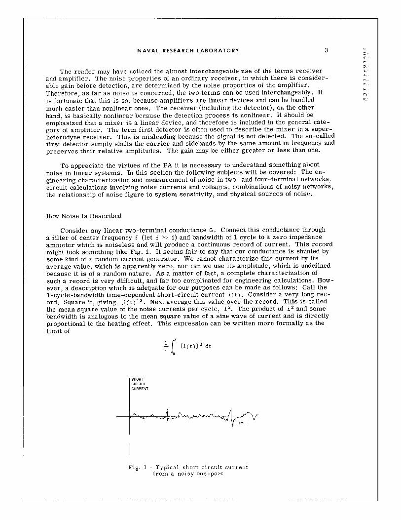
Consider any linear two-terminal conductance G. Connect this conductance througha filter of center frequency f (let f >> 1) and bandwidth of 1 cycle to a zero impedanceammeter which is noiseless and will produce a continuous record of current. This recordmight look something like Fig. 1. It seems fair to say that our conductance is shunted bysome kind of a random current generator. We cannot characterize this current by itsaverage value, which is apparently zero, nor can we use its amplitude, which is undefinedbecause it is of a random nature. As a matter of fact, a complete characterization ofsuch a record is very difficult, and far too complicated for engineering calculations. How-
ever, a description which is adequate for our purposes can be made as follows: Call the1-cycle-bandwidth time-dependent short-circuit current i(t). Consider a very long rec-
ord. Square it, giving [i(t)] 2. Next average this valueover the record. This is calledthe mean square value of the noise currents per cycle, i 2. The product of i
2 and somebandwidth is analogous to the mean square value of a sine wave of current and is directlyproportional to the heating effect. This expression can be written more formally as thelimit of
"f [i(t)] 2 dtT 0
SHORTCIRCUITCURRENT
TIME
Fig. I - Typical short circuit currentfrom a noisy one-port
3C

NAVAL RESEARCH LABORATORY
as T , co. For our purposes, we can assume thatthe random noise source is describedby the value of 12. In general, we must expect i 2 to be frequency dependent; that is, ifthe experiment is repeated with the filter centered at a different frequency we will obtaina different result for i 2 . However, over a narrow band i 2 is constant; thus, for ourpurposes we can assume that i 2 is frequency independent. It should be noted that i 2 hasbeen defined for a bandwidth of 1 cycle. It has been shown that when the bandwidth isdoubled the mean square current is also doubled. Thus, in general, the mean square cur-rent is given by i 2Af, where Af is the bandwidth. Note that the units for i 2 are currentsquared per cycle.
There is a very important theorem concerning the value of i 2 for any conductancewhich is in thermal equilibrium with its surroundings at temperature T. An exact defini-tion of thermal equilibrium is rather difficult to state, but perhaps it would be helpful topoint out that the following two-terminal networks are not at thermal equilibrium: asemiconductor diode drawing current, output terminals of a triode amplifier or mixer, acarbon or metal resistor carrying dc current, and input or output terminals of a firedTR tube. The following could be assumed to be at thermal equilibrium: a carbon ormetallic resistor carrying no current which has been held at a relatively constant tem-perature for a long time, a semiconductor diode at zero bias, and a waveguide matchedload. Nyquist has shown that for these latter devices i 2 = 4kTG, where k is Boltzmann'sconstant. This relationship is completely independent of the physical nature of the device.
Multiply both sides of the above equation by 1/(4G). Then
-= kT. (1)
4G
The left side of Eq. (1) is analogous to the available power from a sine wave gener-ator, and thus the available noise power per unit bandwidth from a one-port or two-terminal conductance at thermal equilibrium of any G is equal to kT. By multiplyingboth sides of Eq. (1) by Af we see that the available noise power from a two-terminalconductance at thermal equilibrium of any G is equal to kTAf.
For two-terminal conductances which are not at thermal equilibrium, there is stillsome value for 12 which describes its noisiness. This can be written as i2 = 4kTnG andwe can consider this a definition of an equivalent noise temperature T". Normally Tn islarger than the ambient temperature of the device.
Circuit Calculations
Consider the following simple problem. Two conductances G1 and G2 , both at roomtemperature To, are connected in parallel and then fed through a lossless filter of band-width Af. What is the short-circuit mean-square noise current at the output of the filter ?This problem involves combining the noise currents of the two conductances to get theresultant mean square current at the output. The proper way to do this is to calculateseparately the effect due to each noise source and add the result. Thus, the mean squarecurrent contribution from noise source one is kT 0 G1 Af and that from noise source twois kT0 G2 Af. The sum of these is kT 0 (G1 + G2 ) Af. Of course, we could have obtained thisresult immediately by observing that the shunt combination of the two resistors (both atthermal equilibrium) is simply a resistor at thermal equilibrium whose conductance isGI+G 2 .
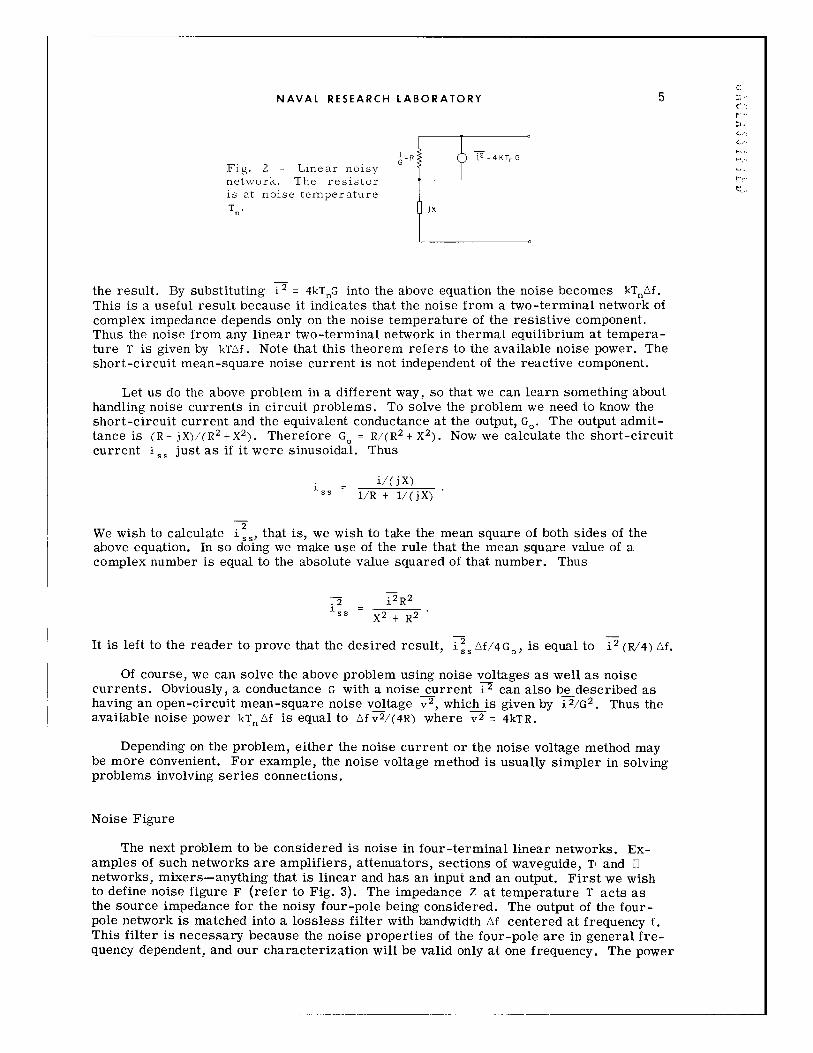
As a second problem we will calculate the available noise power (sometimes calledsimply the noise) of the network of Fig. 2. There is an easy way to do this problem. Ifthe reactance is short-circuited, the noise becomes i 2 (R/4) Af where R = 1/G. Since weare interested in the available noise power, the reactance, being lossless will not affect
4
NAVAL RESEARCH LABORATORY
Fig. 2 - Linear noisy G =R 12 =4KTn,
network. The resistor r!
is at noise temperatureTn. ix
the result. By substituting i 2 = 4kTnG into the above equation the noise becomes kTnAf.This is a useful result because it indicates that the noise from a two-terminal network ofcomplex impedance depends only on the noise temperature of the resistive component.Thus the noise from any linear two-terminal network in thermal equilibrium at tempera-ture T is given by kTAf. Note that this theorem refers to the available noise power. Theshort-circuit mean-square noise current is not independent of the reactive component.
Let us do the above problem in a different way, so that we can learn something abouthandling noise currents in circuit problems. To solve the problem we need to know theshort-circuit current and the equivalent conductance at the output, G.. The output admit-tance is (R- jX)/(R2 +X2 ). Therefore G. = R/(R 2 + X2). Now we calculate the short-circuitcurrent i just as if it were sinusoidal. Thus
- _i/(jX)iss - R
1/R + 1/(jX)
.2
We wish to calculate 1 s, that is, we wish to take the mean square of both sides of theabove equation. In so doing we make use of the rule that the mean square value of acomplex number is equal to the absolute value squared of that number. Thus
.2 i 2 R2
IssSS X
2 + R2
It is left to the reader to prove that the desired result, issAf/4Go, iS equal to i-(,/4) Af.
Of course, we can solve the above problem using noise voltages as well as noisecurrents. Obviously, a conductance G with a noise current i 2 can also be described ashaving an open-circuit mean-square noise voltage v2 , which is given by i2/G2 . Thus theavailable noise power kTn Af is equal to Af v 2/(4R) where v 2 z 4kTR.
Depending on the problem, either the noise current or the noise voltage method maybe more convenient. For example, the noise voltage method is usually simpler in solvingproblems involving series connections.
Noise Figure
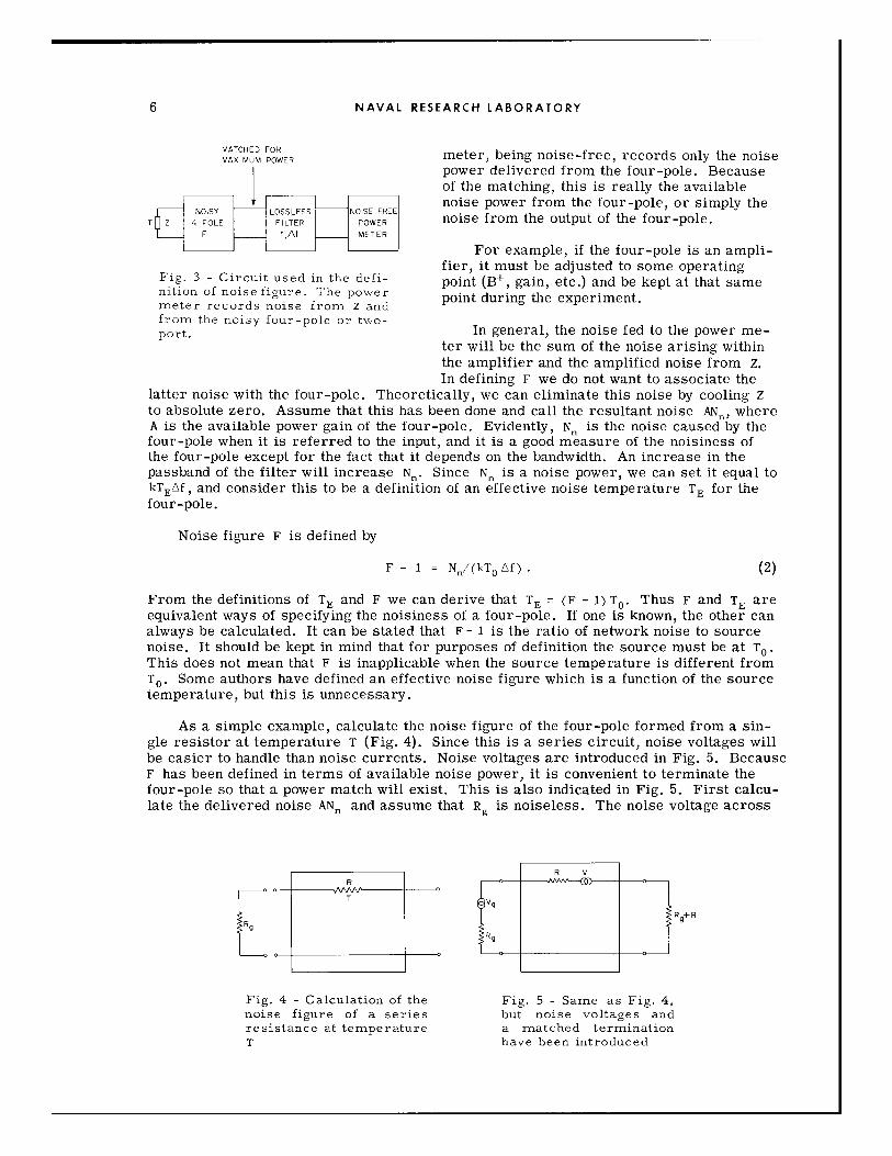
The next problem to be considered is noise in four-terminal linear networks. Ex-amples of such networks are amplifiers, attenuators, sections of waveguide, T and TInetworks, mixers-anything that is linear and has an input and an output. First we wishto define noise figure F (refer to Fig. 3). The impedance Z at temperature T acts asthe source impedance for the noisy four-pole being considered. The output of the four-pole network is matched into a lossless filter with bandwidth Af centered at frequency f.This filter is necessary because the noise properties of the four-pole are in general fre-quency dependent, and our characterization will be valid only at one frequency. The power
5
NAVAL RESEARCH LABORATORY
MATCHED FOR meter, being noise-free, records only the noiseMAXIMUM POWERmee, ni-feolpower delivered from the four-pole. Becauseof the matching, this is really the availablenoise power from the four-pole, or simply the
NOISY - LOSSLESS NOISE FREET 4 POLE FILTER POWER noise from the output of the four-pole.
F fAf METER
For example, if the four-pole is an ampli-fier, it must be adjusted to some operating
Fig. 3 - Circuit used in the defi- point (B+, gain, etc.) and be kept at that samenition of noise figure. The power point during the experiment.meter records noise from Z andfrom the noisy four-pole or two-port. In general, the noise fed to the power me-
ter will be the sum of the noise arising withinthe amplifier and the amplified noise from Z.In defining F we do not want to associate the
latter noise with the four-pole. Theoretically, we can eliminate this noise by cooling Zto absolute zero. Assume that this has been done and call the resultant noise AN,,, whereA is the available power gain of the four-pole. Evidently, Nn is the noise caused by thefour-pole when it is referred to the input, and it is a good measure of the noisiness ofthe four-pole except for the fact that it depends on the bandwidth. An increase in thepassband of the filter will increase Nn. Since Nn is a noise power, we can set it equal tokTE Af, and consider this to be a definition of an effective noise temperature TE for thefour-pole.
Noise figure F is defined by
F - 1 = Nn/(kT0 Af) . (2)
From the definitions of TE and F we can derive that TE = (F - 1) To. Thus F and TE areequivalent ways of specifying the noisiness of a four-pole. If one is known, the other canalways be calculated. It can be stated that F - 1 is the ratio of network noise to sourcenoise. It should be kept in mind that for purposes of definition the source must be at To.This does not mean that F is inapplicable when the source temperature is different fromTo. Some authors have defined an effective noise figure which is a function of the sourcetemperature, but this is unnecessary.
As a simple example, calculate the noise figure of the four-pole formed from a sin-gle resistor at temperature T (Fig. 4). Since this is a series circuit, noise voltages willbe easier to handle than noise currents. Noise voltages are introduced in Fig. 5. BecauseF has been defined in terms of available noise power, it is convenient to terminate thefour-pole so that a power match will exist. This is also indicated in Fig. 5. First calcu-late the delivered noise ANn and assume that R9 is noiseless. The noise voltage across
R
RRR L °Iv Rg+R
Fig. 4 - Calculation of the Fig. 5 - Same as Fig. 4,noise figure of a series but noise voltages andresistance at temperature a matched terminationT have been introduced
6
NAVAL RESEARCH LABORATORY 7
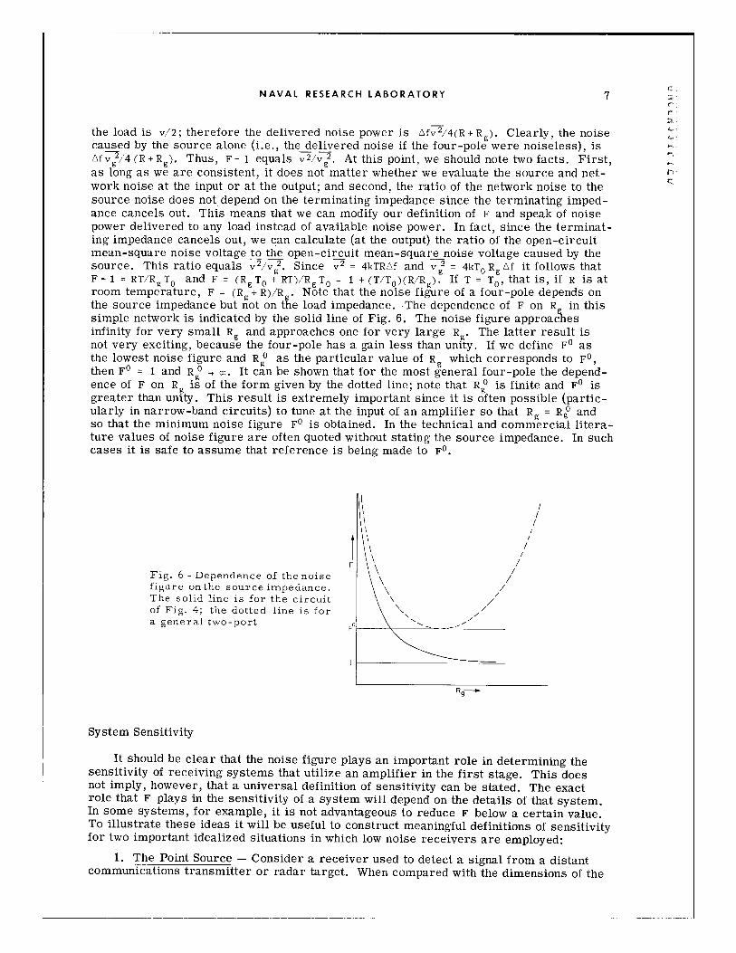
the load is v/2; therefore the delivered noise power is AfV2/4(R+Rg). Clearly, the noisecaused by the source alone (i.e., the delivered noise if the four-pole were noiseless), isAf v 2 /4 (R+R ). Thus, F- 1 equals v2/vg2. At this point, we should note two facts. First,as long as we are consistent, it does not matter whether we evaluate the source and net-work noise at the input or at the output; and second, the ratio of the network noise to thesource noise does not depend on the terminating impedance since the terminating imped-ance cancels out. This means that we can modify our definition of F and speak of noisepower delivered to any load instead of available noise power. In fact, since the terminat-ing impedance cancels out, we can calculate (at the output) the ratio of the open-circuitmean-square noise voltage to the open-circuit mean-square noise voltage caused by thesource. This ratio equals v2/v 2. Since v 2 = 4kTRAf and v 2 - 4kT Rg Af it follows thatF-1 = RT/RgT 0 and F= (RgTo + RT)/ gT 0 z 1 + (T/To)(R/Rg). If T = To, that is, if R is atroom temperature, F = (R + R)/R . Note that the noise figure of a four-pole depends onthe source impedance but not on t&e load impedance. The dependence of F on R g in thissimple network is indicated by the solid line of Fig. 6. The noise figure approachesinfinity for very small Rg and approaches one for very large R . The latter result isnot very exciting, because the four-pole has a gain less than unity. If we define FO asthe lowest noise figure and R 0 as the particular value of R which corresponds to F0 ,0g gthen FO - 1 and R ° -, o. It can be shown that for the most general four-pole the depend-ence of F on Rg is of the form given by the dotted line; note that R 0 is finite and FO isgreater than unity. This result is extremely important since it is often possible (partic-ularly in narrow-band circuits) to tune at the input of an amplifier so that Rg = R 0 and
gso that the minimum noise figure FO is obtained. In the technical and commercial litera-ture values of noise figure are often quoted without stating the source impedance. In suchcases it is safe to assume that reference is being made to FO.
/F/
Fig. 6 - Dependence of the noise /figure onthe source impedance.The solid line is for the circuit /of Fig. 4; the dotted line is for 1/a general two-port F"
System Sensitivity
It should be clear that the noise figure plays an important role in determining thesensitivity of receiving systems that utilize an amplifier in the first stage. This doesnot imply, however, that a universal definition of sensitivity can be stated. The exactrole that F plays in the sensitivity of a system will depend on the details of that system.In some systems, for example, it is not advantageous to reduce F below a certain value.To illustrate these ideas it will be useful to construct meaningful definitions of sensitivityfor two important idealized situations in which low noise receivers are employed:
1. The Point Source - Consider a receiver used to detect a signal from a distantcommunications transmitter or radar target. When compared with the dimensions of the
NAVAL RESEARCH LABORATORY
transmitting antenna or the radar target the receiving antenna pattern is very broad.The receiving antenna, therefore, must be looking not only at the signal source but alsoat a background which almost completely determines the impedance of the antenna as wellas the noise temperature associated with the antenna. The effective noise temperature ofthe antenna or the effective temperature of the radiation resistance of the antenna will bean average of the space at which the antenna is looking. For example, if an antenna isaimed at the sea, it is reasonable to assume that its noise temperature would be equal tothe temperature of the sea.
This antenna noise must be considered a disturbing factor in the attempt to detectthe signal from a distant transmitter or radar target. However, the important point isthat if the distant transmitter or radar target were suddenly removed, the effect on theantenna impedance and temperature would be negligible. This example then is that of apoint source imbedded in a thermal noise background.
The total noise power referred to the input of the receiver is Nn + kTAf where asbefore Nn is the network or amplifier noise and T is the noise temperature of the antenna.
Also N. is given by Eq. (2); thus, the total noise equals kAf [(F - 1) To + T]. It follows thatif the total noise is doubled, the signal to noise ratio will be halved; or if the total noiseis halved, the signal to noise ratio will be doubled. It seems reasonable to define thesensitivity S of the system as the inverse of this quantity. Boltzmann's constant k andthe bandwidth Af can be dropped, because they are not relevant. We then have
S (F- 1)To + T (3)
For the case in which the antenna temperature T is equal to the room temperatureTO , then
S (4)FTo
This is one case, at least, in which the sensitivity is dependent upon F alone. The sensi-tivity of a radar or communications receiver whose antenna is at temperature To, is in-versely proportional to the noise figure.
As a second case assume T is well below room temperature. This is possible be-
cause at certain microwave regions parts of the sky are cold. But if we exaggerate thesituation and assume that T = 0 we have the extremely interesting result that S is in-versely proportional to F- 1. In other words a receiver of noise figure 1.05 is twice assensitive as a receiver of noise figure 1.1.
As a final case, assume that T is very large. As T , co, S = 1/T and the sensitivityis independent of the noise figure of the receiver.
2. The Extended White Noise Source - Assume that one points a radio astronomyantenna at a broadband radio source of noise temperature T, (for example, the sun) andwishes to measure T . If the antenna beam is too wide, noise sources around the objectof interest will be picked up and the situation will become complicated. If, on the otherhand we assume that the antenna beam is narrow and includes only the source of interest,a reasonable definition of sensitivity can be given: Sensitivity is defined to be the ratioof the available signal power to the available amplifier noise power at the amplifier out-put. In this definition atmospheric absorption is neglected, and T. is assumed to be inde-pendent of frequency over the bandwidth of the receiver. The noise from the source isnow the signal (note that the signal/is what we choose it to be) and it is degraded as itpasses through the amplifier. Again using Eq. (2) we will have S = AfAkTI [Af AkT 0 (F- 1)],where A (which cancels out) is the available gain of the receiver and
8
NAVAL RESEARCH LABORATORY 9
r
S = T/ [To(F- 1)1
Thus
So0CF-1
This simple relationship indicates why radio astronomers are so intensely interested insuper-low noise receivers. For example a receiver of noise figure 1.01 is ten timesbetter than one of noise figure 1.1.
But what does the discussion of system sensitivity have to do with parametric ampli-fiers ? This question will be answered more fully later but a partial answer will be givenat this point. When a receiver problem for some particular system is formulated, theengineer may be asked to select the most appropriate type of receiver. It would befoolish to select the maser for an application which did not really require a very lownoise figure. Thus the engineer must know something about the relationship betweennoise figure and system sensitivity if he is to choose properly.
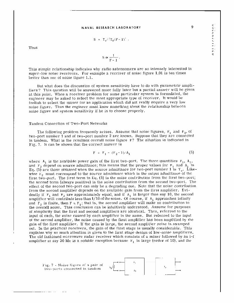
Tandem Connection of Two-Port Networks
The following problem frequently arises. Assume that noise figures, F, and F 2 , oftwo-port number 1 and of two-port number 2 are known. Suppose that they are connectedin tandem. What is the resultant overall noise figure F? The situation is indicated inFig. 7. It can be shown that the correct answer is
F = F 1 + (F 2 - 1)/A 1 (5)
where A1 is the available power gain of the first two-port. The three quantities F 1, A1,and F2 depend on source admittance; this means that the proper values for F1 and A, inEq. (5) are those obtained when the source admittance for two-port number 1 is Y.. Like-wise F 2 must correspond to the source admittance which is the output admittance of thefirst two-port. The first term in Eq. (5) is the noise contribution from the first two-port;the second term (always positive) is the noise contribution from the second two-port. Theeffect of the second two-port can only be a degrading one. Note that the noise contributionfrom the second amplifier depends on the available gain from the first amplifier. Evi-dently if F1 and F 2 are approximately equal, and if A1 is larger than say 10, the secondamplifier will contribute less than 1/10 of the noise. Of course, if A1 approaches infinityand F2 is finite, then F :. F1; that is, the second amplifier will make no contribution tothe overall noise. This conclusion can be intuitively understood. Assume for purposesof simplicity that the first and second amplifiers are identical. Then, referred to theinput of each, the noise caused by each amplifier is the same. But referred to the inputof the second amplifier, the noise caused by the first amplifier has been amplified by thegain of the first amplifier. If the gain is large, the second amplifier noise is swampedout. In the practical receivers, the gain of the first stage is usually considerable. Thisexplains why so much attention is given to the first stage design of low-noise amplifiers.The old fashioned microwave radar receiver which consists of a mixer followed by an i-famplifier at say 30 Mc is a notable exception because F1 is large (order of 10), and the
Fig. 7 - Noise figure of a pair of [ Fý F 2
two-ports connected in tandem As

NAVAL RESEARCH LABORATORY
mixer is actually lossy (A, is of the order of 1/4). Thus, the noise figure of the second
stage, which in this case is the i-f amplifier, must be low for a low overall F.
It has already been pointed out that noise figure is a good figure of merit for the
noise behavior of four-terminal networks. This statement should be amended to state
that noise figure is a useful figure of merit provided that the network has high gain. It
is, after all, the overall noise figure of an entire receiver that is important, and it is of
small value to have a low noise figure in the first stage if the gain is so low that the noise
from the second stage predominates. For example, suppose that an engineer is intrigued
by the fact that a network of pure inductances has a noise figure of one, and thus decides
to use such a network as a first stage in a receiver. Since power is not lost in such a
network the matched power gain or available gain A1 is also equal to one. Applying Eq.
(5), we see that the overall noise figure is equal to the noise figure of the second stage.
For a stage of only moderate gain it seems that there should be some sort of noise figure
of merit which would properly take into account the gain as well as the noise figure. Such
a figure of merit exists; it is called the noise measure and will be discussed later. How-
ever, as far as complete amplifiers, composed of many stages, are concerned the gain is
always very high; thus the noise figure is a perfectly valid figure of merit.
Some remarks are in order here concerning the laboratory adjustment of receivers
for overall minimum noise figure. Refer again to Eq. (5) and Fig. 7, but assume, as is
often the case, that there are transformers between Y. and the input to the first stage,
and between the first and second stage.
With reference to Eq. (5) it is pertinent to ask how the above system can be adjusted
to produce a minimum overall noise figure. The interstage transformer is easily ad-
justed. We adjust this transformer until the source conductance seen by the second am-
plifier is the optimum source conductance GO. Then by definition, F 2 will assume its
smallest value. If we assume that this transformer is lossless, this adjustment will have
no effect on F1 or A,. However, adjustment of the input transformer will affect both A1
and F1 . We would like to adjust A1 to be very large (to its maximum value if it exists),
and, at the same time, we would like Fi to equal its minimum value F0. Unfortunately,
the nmaximum value of A1 is not obtained for that source admittance which minimizes F 1 .
That is, "tuning for maximum power gain is different from tuning for minimum noise fig-
ure." In practice, this problem can be solved in the laboratory by tuning the input trans-
former for minimum overall noise figure. Since even one measurement of noise figure
is time consuming, this can become a laborious task.
QUALITATIVE DESCRIPTION OF PARAMETRIC AMPLIFICATION
The heart of the parametric amplifier (PA) is the capacitance C which varies with
time at the pump frequency f 3 . The reason for using the symbol f 3 for pump frequency
will become clear in a later paragraph. There is, of course, no such thing as a capaci-
tance without losses, but it is a useful idealization and we will first assume that such a
capacitor is available. We will see later that the losses in real capacitors constitute the
main limitation in PA operation.
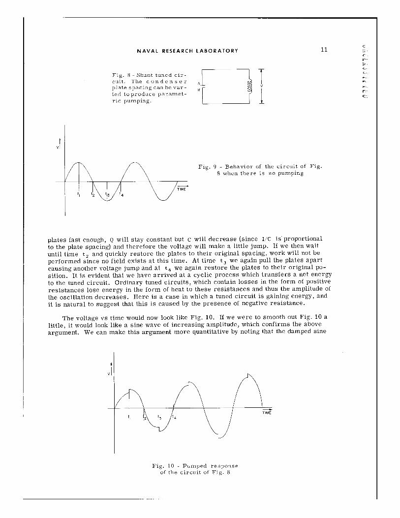
We can gain insight into the PA process by considering the circuit of Fig. 8. As-
sume that this circuit is oscillating at its resonance frequency fo = 27T 0 . Since there
are no losses, it will continue to oscillate at the same amplitude and frequency for an in-
definite period, as shown in Fig. 9. We now wish to describe the pumping process. Suppose
that at time ti of Fig. 9 we suddenly pull the plates of the condenser apart and hold them
at this new separation. This certainly will take mechanical work, and since energy must be
conserved, it would appear that we have transferred some mechanical energy into electri-
cal energy in the form of the electric field of the condenser. The voltage across the con-
denser is given by V = Q/C where Q is the charge on the condenser. If we move the
10
NAVAL RESEARCH LABORATORY
Fig. 8- Shunt tuned cir-cuit. The condenserplate spacing can be var-
ied to produce paramet-ric pumping.
C..,
A IB1
I
Fig. 9 - Behavior of the circuit of Fig.8 when there is no pumping
TIME
t t2 f 3
plates fast enough, Q will stay constant but C will decrease (since 1/C is proportional
to the plate spacing) and therefore the voltage will make a little jump. If we then wait
until time t 2 and quickly restore the plates to their original spacing, work will not be
performed since no field exists at this time. At time t 3 we again pull the plates apart
causing another voltage jump and at t 4 we again restore the plates to their original po-
sition. It is evident that we have arrived at a cyclic process which transfers a net energy
to the tuned circuit. Ordinary tuned circuits, which contain losses in the form of positive
resistances lose energy in the form of heat to these resistances and thus the amplitude of
the oscillation decreases. Here is a case in which a tuned circuit is gaining energy, and
it is natural to suggest that this is caused by the presence of negative resistance.
The voltage vs time would now look like Fig. 10. If we were to smooth out Fig. 10 a
little, it would look like a sine wave of increasing amplitude, which confirms the above
argument. We can make this argument more quantitative by noting that the damped sine
vt
TIME
I t t4
Fig. 10 - Pumped responseof the circuit of Fig. 8
nn
I/
11
Vý
tII V/

NAVAL RESEARCH LABORATORY
wave of a normal tuned shunt circuit is of the form (sin (i 0t) exp (-Gt/2C). Ordinarily G
is positive, but if we let it be negative then we have an exponentially increasing sine wave.
In other words, when a shunt tuned circuit is 'shunted with a negative conductance we obtain
a sine wave of increasing amplitude. Thus, the effect of pumping the circuit of Fig. 8 is
as if we had placed a negative conductance across the tuned circuit.
It is important to note that the plates must be separated at special times during the
resonance cycle of the tuned circuit. That is, the pump frequency must have a definite
relationship to the resonance frequency. In the example given, the pump frequency is just
twice the resonance frequency. The observant reader will notice, however, that although
pumping at twice the resonance or signal frequency is most efficient, it is not really nec-
essary to pump every cycle in order to obtain some increase in amplitude as long as the
plates are separated at the right times. Pumping at frequencies lower than the signal
frequency is called harmonic pumping.
Once we have established the fact that pumping can produce an equivalent negative
conductance, it follows immediately that either an amplifier or an oscillator can be built
at 1/2 the pump frequency, depending on the external circuit loading. Even from this sim-
ple model, we can see what some of the characteristics of PA's must be. They must be
of the negative resistance type (and thus have stability problems), they must be narrow
band (at least in single-tuned versions), and we can perhaps even guess that they will be
low noise since ordinary pure capacitances do not produce noise.
There is, however, a subtle flaw in the above reasoning. It is absolutely required
that there exist an exact relationship between the pump frequency and the signal frequency;
for example the signal frequency must be exactly 1/2 the pump frequency. This implies
complete knowledge of the signal phase at all times. But ordinarily one does not have
such knowledge of real signals. The flaw may be explained in another way. Suppose that
the signal is amplitude modulated. The requirement that the pump frequency be twice the
signal frequency cannot be met when there are sidebands to deal with. It is therefore
clear that what we have been describing is not really an amplifier in the usual sense of
the word. It may be described as a lock-in amplifier. The lock-in amplifier does have
certain uses, but we are mainly interested in low-noise amplifiers, in the usual sense, so
we will not pursue this matter further.
It should be emphasized that the difficulty is not with the circuit of Fig. 8 but rather
with the above primitive argument leading to the conclusion that the signal frequency has
to be exactly 1/2 the pump frequency. In a more correct treatment, it will be convenient
to refer to Fig. 11. Assume that C is pumped at that frequency f 1 + f 2 = f 3 , which is the
sum of the resonant frequencies of the two tanks. (Note that Fig. 8 is a special case of
Fig. 11 in which f 1 = f 2.) It can be shown that under these conditions, then, looking to
the right at AA' at a frequency f we see a pure negative conductance and looking to theleft at BB' at frequency f 2 we see a differentpure negative conductance. Thus, both tanks
oscillate simultaneously at their respectiveA fl +f2 resonant frequencies.
SI I To make an amplifier both tanks must be
i properly loaded. An amplifier can be con-structed to operate at either f 1 or f 2. The
unused frequency is called the idler frequency.
I It is important to realize that currents and
I I voltages always exist in the idler tank at thefi A' B' f2 idler frequency. Suppose we choose to construct
a negative conductance at f 1 . (We will defer a
Fig. 11 - Two-tank discussion of how two-terminal negative con-
narametric circuit ductances or resistances can be used as
12

NAVAL RESEARCH LABORATORY
amplifiers.) The circuit is as shown in Fig. 12. PUMP
Note that the idler tank is loaded by the conduct-ance Gi. This is absolutely necessary for para-metric behavior. Suppose the pump frequency isadjusted to equal f1 + f 2. We want the signal fre- NEGATIVE
quency f. nearly equal to fl,butwe certainly can- -C
not guarantee that this will be the case; in fact, wemust assume that they will differ slightly. Aproper solution of this problem shows that a nega- Fig. 12 - The generation oftive conductance will appear across tank 1 pro- a negative conductancevided only that f s + f i equals the pump frequencyf 3, where fI is the frequency of currents and volt-ages appearing in tank 2. Note that since f1 I f{we have f 2 ý fI. Note also that we are assuming the circuit is in the nonoscillating con-dition. The frequency fI is actually generated by a mixing action between f and f3;thus the condition fr + f = f 3 is automatically satisfied. Of course, for significant gain,it is necessary for f , and f1 to remain within the passband of their respective tanks,so that the device is still narrow-banded. We are now dealing with a negative conduct-ance which can be built into an amplifier.
The above was a physical explanation of the negative resistance parametric ampli-fier. Unfortunately, a simple physical explanation of the stable upconverter is not possi-ble, and we will need to carry out a quantitative analysis of this device before we canproceed.
PARAMETRIC OR VARACTOR DIODES
In practice one cannot vary the plates of a capacitor fast enough for amplifier opera-tion. An electronic method of varying a capacitance is required. Until recently such adevice was not available. The principle of parametric amplification has in fact beenknown for some time, but the development of the modern low-noise parametric amplifierhad to await the invention of the pn junction parametric diode.
The property of the pn junction that interests us is as follows: When a pn junctionis biased in the back direction, nearly zero current is drawn. The diode is capacitative,however, and the value of the capacitance depends on the instantaneous value of the appliedvoltage in the manner indicated by the dashedcurve in Fig. 13. The solid curve is currentvs voltage at low frequency. The back voltageat which the current rises sharply is calledbreakdown voltage VB* It is an important pa- /1rameter because we must operate between zerovoltage and vB in order to avoid drawing cur-rent and to keep the capacitance essentially //lossless.
If we bias the diode approximately halfway Lbetween zero and vB and apply a sinusoidalvoltage of amplitude VB/2 and frequency f 3 wewill get the largest possible variation of C vstime. Filters may be necessary to keep f 3separate from the signal frequency, but, exceptfor this slight difficulty, this is a perfectly ac-ceptable way of producing a condenser whosevalue varies at .f3 Fig. 13 -Current (solid curve)
and capacitance (dotted curve) ofAll real parametric diodes have a spread- typical pn junction as a function
ing resistance Rs in series with the nonlinear of voltage
13

NAVAL RESEARCH LABORATORY
capacitance. This resistance is, to a good approxima-tion, frequency and bias independent. The equivalent
Rs circuit is shown in Fig. 14, where the arrow through the
ci r cuit of back- capacitance indicates that C is voltage dependent. The
biased varactor or effect of R, is to degrade the signal performance of theparametric diode diode. This degradation becomes worse as the frequency
c rises, and for very high frequencies C behaves as ashort-circuit; when this happens only R, is left whichcannot produce parametric effects. In addition, R makesa noise contribution and degrades the noise figure. It is
useful to define a cutoff frequency f. as that frequency atwhich the magnitude of the capacitative reactance is equal to R,;. Thus, R, = 1/(2 fEC')gives f = 1/(2 RsC'). It will be shown later that a special capacitance Co should appearin the above formula. In practice, however, manufacturers define fc in terms of thevalue of the diode capacitance for some particular back bias, and we denote this by C'.The value of f, so defined is close to the correct value, which is obtained when Co isused. Unfortunately, there is no universal agreement as to what bias to use in definingC'. Various authors use zero bias, VB, VB/2 or some arbitrary value. Still f is auseful figure of merit for a PA diode, or, as it is sometimes termed, a varactor diode.Cutoff frequencies for commercially available diodes go up to the order of 200 kMc. Asa rough approximation we can say that an acceptable amplifier can be built at 1/10 thecutoff frequency.
GENERAL THEORY OF SMALL SIGNAL NONLINEAR CAPACITANCE
Introduction
We now begin a quantitative study of the properties of the nonlinear capacitor. Thereader may wonder why the term nonlinear capacitor is used instead of time-varyingcapacitor, which was previously employed. This is because the only practical methodwe have of producing a time-varying capacitor at high frequency is by using the pn junc-tion diode. The pn junction exhibits a time-varying capacitance only because its capac-itance is a function of the applied voltage; that is, it is a nonlinear capacitance.
It has been mentioned that a nonlinear capacitor may be used for amplification inseveral different ways or modes. We decided to use the term parametric amplifier (PA)to include these different ways. However, we are going to make a special study of twocircuits: the upper sideband upconverter, hereafter called the upconverter, and the nega-tive resistance parametric amplifier, hereafter called the NRPA. As one might guess,the upconverter is really a mixer with gain, but unlike the usual mixer the output fre-quency is higher than the input frequency. The upconverter is perfectly stable; that is,there is no combination of source and load impedance and no change in diode character-istics which will make it oscillate. The properties of the NRPA are different. The inputand output frequencies are the same, in fact, the input and output terminals are identical,and it will oscillate if loaded improperly. What is the point, then, in discussing both ofthem in the same section? It is because their properties as well as the properties ofseveral modes, which we are not going to discuss in detail, arise fundamentally from thenonlinear capacitor. Thus the first steps are the same regardless of the mode of operation.
The key idea here is that any form of PA is intrinsically a multifrequency device.This is true even if the same frequency is found at both the input and output terminals.In the case of the NRPA, for example, which has a common input and output frequency, itcan be shown that both current and voltage at the idler frequency must be present for thedevice to operate; in fact, power must be dissipated at the idler frequency. Either cur-rents or voltages must be present at many other frequencies, but normally these channelsmay be either open or short-circuited so that power is not dissipated at these frequencies.
14
NAVAL RESEARCH LABORATORY
The easiest way to short-circuit or open these unused frequencies is to use tuned cir-cuits for the frequencies at which power must be dissipated, but this results in a narrow-band device. Those readers who have some familiarity with the conventional microwavemixer will find that it is similar in many ways to the PA.
Mixing in the Nonlinear Capacitance
Let us examine the consequences of the mixing action of a nonlinear capacitance.The problem is greatly simplified if we assume that the pump voltage is large whencompared to the signal voltage. This is tantamount to the assumption that as far as thesignal is concerned the capacitor is linear; that is, the value of the capacitor is notchanged by the signal voltage. This is similar to the assumption made in treatingvacuum-tube or transistor amplifiers. If the signal voltage is small enough the ampli-fier may be treated as a linear four-pole. No distortion and no harmonics of the inputfrequency appear at the output. But when the signal becomes large, as it may in a poweramplifier, we expect distortion and new frequency components in the output. Thus, theamplification factor /i of a vacuum tube depends on the value of the supply voltage butdoes not depend on the signal amplitude if the signal amplitude is below a certain level.In the same way we can say that the properties of the capacitative mixer (i.e., the waythat the capacitance changes with time) depend on the pump but not the signal.
Assume then that the capacitor C is driven by a high level pump at frequency f 3 andalso by a low level signal at frequency f 1 . We do not wish to say at this point whetherthe f 1 "signal" is the input, the output, or neither. Assume that f 1 is the lowest fre-quency low-level signal. Consider only normal pumping, then f 1 < f 3. Because of themixing process, a set of low level signals will be generated whose frequencies are givenby nf 3 ± f, where n is any integer. In addition there will be a set of high level frequen-cies generated which are simply the harmonics of the pump frequency. This is given bymf 3 , where m is any integer. However, we are not interested in these frequencies sincethey are not associated with any signal but instead with pump or B+ supply.
Note that we must deal with an infinite set of low level frequencies since n can as-sume any value. This is not a very desirable situation either from the theoretical orpractical point of view. If the energy of the input signal were to be converted into a largenumber of new frequencies and then dissipated at these frequencies we could hardly ex-pect low noise and high gain to result. A way out of this difficulty is to short-circuit oropen all those frequencies which are not needed. This will prevent the dissipation ofpower at the unused frequencies. If we assume that this is done it can be shown that, inthe theoretical treatment, we can completely ignore these unused frequencies.
It is one thing to assume that the above can be done and quite another thing to do itin a practical amplifier. The fact that amplifiers can be built with properties closelyapproximating those predicted by the simplified theory indicates that the unused frequen-cies are being effectively suppressed. It turns out that to account for the parametricphenomena of interest we need to consider only three frequencies, namely fl, f 2 = f 3 - fj,and f 4 - f 3+ fl"
The above argument exactly parallels the treatment of the conventional radar micro-wave mixer, in which typical values might be f1 = 30 Mc, f 3 = 10,000 Mc, and thus theother "signal" frequencies would be f 4 = 10,030 Mc and f 2 = 9970 Mc. In this case f,is the output i-f frequency and either f 2 or f4 is the input microwave frequency. Inthis particular case, it makes little difference whether the upper sideband f 4 or thelower sideband f 2 is chosen for the input, because this mixer is a resistive mixer ratherthan a capacitative mixer. However, something must be done about the sideband which isnot chosen for the input. It may be short-circuited thus giving the lowest noise figure.Unfortunately, this reduces the bandwidth (since a filter must be employed). This is
15

NAVAL RESEARCH LABORATORY
AMPLITUDE1
f2 f3FREQUENCY -
Fig. 15 - Frequency spectrum of aparametric amplifier. In practice,either f 2 or f4 is reactively termi-nated.
called narrow-band operation, and it isequivalent to considering this sideband asan unused frequency. If no filter is usedthe unused sideband is terminated in thesame way that the input frequency is ter-minated, namely with the source imped-ance.* Since no signal enters this unusedchannel, but noise associated with thesource resistance does enter, this noisefigure is higher than the narrow-bandnoise figure.
Let us return to the capacitativemixer. Figure 15 shows the frequencyspectrum we are now treating. The readermay convince himself that since f1 is bydefinition the lowest signal frequency, itcan at most equal 1/2 f 3 ' The problemnow consists of determining the relation-ships which the pumped capacitor imposesbetween the voltages and currents at thethree frequencies of interest. Since we
assumed these currents and voltages are very small, it is natural to assume that theserelationships will be linear, just as the relationships between the various currents andvoltages in vacuum-tube or transistor amplifiers are linear. Let I1, V1 , I2, V 2 , 14,
and V4 denote the complex amplitudes of the currents and voltages at the angular fre-quencies W1, w2, and co4. Then, assuming that the unused frequencies are short-circuitedit can be shown (2a) that the relationships we seek are of the form
14 = j&)4 CoV 4 + joi4 C 1 V 1 + joa4 C 2 V2
(6)
= -2C2V4 - jiC2 C 1 V 1 - jw 2 CoV2
where the asterisks indicate the complex conjugate. The real numbers Co, C1 , and C 2will be defined presently.
2 2
Fig. 16 - Three-port whichrepresents the capacitativemixer. Each port is at adifferent frequency.
These equations contain all the information re-lating to the signal properties of any of the more fre-quently used modes of parametric amplification, andin a sense they even include the noise properties. Itmust be remembered, however, that these equationsrefer to the pure nonlinear capacitor; that is, theeffect of the spreading resistance is not included.
At this point, we are dealing with a linear six-pole or three-port device, and the properties of suchnetworks have been extensively treated in the litera-ture. The three-port device is indicated in Fig. 16.This sketch should emphasize the fact that this three-port is similar to other three-ports, except that thesame frequencies do not appear at each port.
*This is because there are no microwave components left in the circuit which can distin-guish between the two sidebands.
I1 = jwcoClV 4 + jcd1lCoV 1 + ji6 1 C1 V*
16
NAVAL RESEARCH LABORATORY
Various Operating Modes 411
Various amplifiers and converters can be formed from the three-port of Fig. 16 bychoosing a port for the input, a port for the output (the input and output may be the same nport) and by connecting passive loads to the unused ports. For example, there are six 'Z
possible choices for converters if we require that the input and the output be differentports. They are:
1. Input at port 1, output at port 4.
2. Input at port 4, output at port 1.
3. Input at port 2 and output at port 4.
4. Input at port 4 and output at port 2.
5. Input at port 1 and output at port 2.
6. Input at port 2 and output at port 1.
Note that all these are converters (they shift frequency) since no two ports are at thesame frequency. But this still does not indicate all the variations possible in converters.Consider, for example, 1 above. The properties of this converter will depend on whattype of passive load is connected to the unused port 2. If port 2 were loaded resistively,for example, the converter would, in general, behave differently than if port 2 were reac-tively loaded.
Even though there are in theory many modes of operation, most of these modes arenot practical for one reason or another. For example some modes do not result in gainbut rather in loss.
Let us now discuss these various modes in some detail and indicate which ones arepractical. Later we will treat in still further detail the upconverter and the NRPA. Fornow, statements will be made without proof; later some of these statements will be proved.
Converters will be discussed first. The unused frequency or the unused channel isalways terminated by a short-circuit or an open circuit. It really does not make muchdifference which choice is made, but we will assume that the unused channel is short-circuited. Thus, we need to consider only the six choices listed above. Neither choice4 or 2 are used because they result in loss rather than gain. Thus downconversion fromthe upper sideband is never used. Furthermore 3 is never used because it results inlow gain. There is only one scheme left which uses the upper sideband, and this is 1,which is called the upper sideband upconverter or often just the upconverter. The max-imum possible power gain is given by f4/ f; thus, the input frequency must be smallcompared to the pump frequency if significant gain is to result. The upconverter is themost broadband mode and it is completely stable; that is, it will not oscillate for anycombination of load and source impedance. Although infinite gain is possible in 6, it isnot used because it is unstable. This leaves 5, which is a lower sideband upconverter(compare it with 1). In principle it is an attractive mode although it has not been usedoften. Infinite gain and low noise are possible in this mode. It is inherently a narrow-band converter compared with the upper sideband upconverter, and it is not stable forsome combinations of source and load impedance. It also has the following peculiarity:Since the sum of the input and output frequencies equal a constant f 3 , modulation side-bands which appear above the carrier at the input will appear below the carrier at theoutput. This is called sideband inversion, and it may not be acceptable in some systems.The only converter which seems worthy of further discussion then is the upconverter.
17
18 NAVAL RESEARCH LABORATORY
We now turn to single-frequency amplification. How can we make an amplifier, as
distinguished from an amplifying converter? Clearly the same port must serve as both
the output and the input, but the only way that a one-port can be used for amplification is
for it to have negative conductance or resistance. It turns out that no matter how ports
I and 2 are terminated, only positive resistance appears at port 4. Thus negative resist-
ance cannot appear at a frequency higher than the pump frequency. There are two modes
of operation which will yield a one-port or two-terminal negative resistance.
1. Short-circuit port 4, terminate port 2 resistively and a negative conductance
appears at port 1.
2. Short-circuit port 4, terminate port 1 resistively and a negative conductance
appears at port 2.
Note that in both cases f 4 simply becomes another unused frequency and can be
ignored. Furthermore, it can be shown that 2 results in a higher noise figure, and in
fact, is never used. We call mode 1 the negative resistance parametric amplifier or
NRPA. It is the most popular form of parametric amplification.
It might appear to be better to terminate p, rt 2 by a short-circuit or open-circuit
rather than resistively. It turns out, howevel, 'hat the negative resistance will appear
at port 1 only if port 2, often called the idler, 's terminated resistively. This can per-
haps be understood intuitively from the follcv.x;ng: If f 2 is short-circuited (and remem-
bering that the unused frequencies are also short-circuited), then from the point of view
of an observer at port 1, the whole device becomes completely reactive, that is, it could
not have a resistive component because there is no loss mechanism. Thus the input ad-
mittance at port I is purely reactive. The nonlinear capacitor when employed in this
manner can be thought of as a transformer which transforms the positive conductance or
resistance of the idler circuit into a negative conductance or resistance at port 1.
In summary, there are only two commonly used modes of parametric amplification:
1. The upconverter which has input at f 1 and output at f 4 . The output frequency f 4
must be large with respect to f, since the maximum possible gain is f4 /fl. This means
that the pump frequency f 3 must also be large since it is given by f 4 - f 1 _ f 4 " In prac-
tice, the gain is usually somewhat less than f 4/f 1 , which forces the pump and output fre-
quencies up still further to realize a given gain. The upconverter is completely stable
and it is the most broadband mode. There are many situations in which the frequency
shift is not acceptable. Suppose, for example, that we want to put a low-noise preampli-
fier on an existent radar receiver in order to improve the radar range. A converter
could not be used because the input and output frequencies of the preamplifier must be
the same. On the other hand if we design a low noise receiver from scratch with only
the input frequency specified, there would be no objection to the use of a low-noise up-
converter first stage followed by a conventional amplifier at f 4 "
2. The NRPA. The input and output frequencies are the same. The gain can be very
high, but the result is gain instability and the possibility of oscillations. Power must be
dissipated at an idler frequency, which is equal to the pump frequency minus the signal
frequency. The NRPA is relatively narrow-band.
Properties of the Three-Port Nonlinear Capacitance Mixer
In order to quantitatively treat the upconverter and the NRPA we must reconsider
Eq. (6), which describes the three-port from which these devices are constructed. The
properties of the three-port (which in turn determine the properties of the upconverter
and the NRPA) are contained wholly in the coefficients of the voltages on the right side

NAVAL RESEARCH LABORATORY 19
r
of Eq. (6). It is convenient to arrange these coefficients as shown below and to call this 4
array the admittance matrix Y of the three-port. Thus,
Sw4 CO w~4 C 1 4 .C2
Y j- cl jcolc 0 j 1jcW 1 (7)
-Jw2 C2 - jiW2 C1 -j-2 2 CO)
We need to discuss this admittance matrix, but first we should note one peculiar fea-ture about Eq. (6). The current and voltage corresponding to the lower sideband appearas complex conjugates. This is a result which is necessary if negative frequencies areto be avoided, and will cause no difficulty.
First note that all the elements of Y are pure imaginary numbers. This seems rea-sonable because Y was constructed from a lossless nonlinear capacitor. In fact eachterm of Y has the form of the admittance of a capacitor. Note also that each row of Ycontains only one frequency; for example, the second row (which is really the f1 row)contains only the frequency f 1l
Finally, we see that the element of the first row, second column is not equal to theelement of the first column second row and so forth. Networks in which this is the caseare called nonreciprocal. There is a very fundamental difference between nonreciprocaland reciprocal networks. Nonreciprocal networks have a "one way" feature in that themaximum power gain differs when the input and the output are interchanged. Examplesof reciprocal networks are (a) networks consisting only of resistances, capacitances, andinductances, and (b) passive microwave circuits without static magnetic fields, etc. Ex-amples of nonreciprocal networks are vacuum-tube and transistor amplifiers, microwaveisolators, and microwave circulators.
Consider the real parameters C0, C1, C2. These arise as follows: The local oscil-lator voltage causes a periodic variation of capacitance. This depends on the C vs Vcurve of the diode (see Fig. 13) and on the local oscillator voltage waveform. Thus, C isa periodic but, in general, a nonsinusoidal function of time (i.e., C = C(t)). Therefore,C(t) may be expanded in a Fourier series. The problem is greatly simplified if it isarbitrarily assumed that C(t) is an even function, which is the same thing as saying thatwe can leave out the sine terms in the expansion. Thus,
C(t) -= Co + 2C 1 cos cW3 t + 2C2 cos 2w 3 t + ...
In words, the C' s are one-half the Fourier coefficients of the expansion of the capaci-tance as a function of time. It is important to note that the C's depend on both the non-linearity law of the capacitance and on the pump waveform. If the capacitance is linear,that is if C does not depend on V, then C(t) will simply be a constant and C,, C21 ...will equal zero. What does Eq. (6) have to say about this situation? Suppose a voltage V1is applied at port 1. The first row gives 14 = 0, the second row gives I1 = j w Co v 1 , andthe third row gives 12 = 0. In other words, there is neither coupling between ports normixing action. This is just what is expected of an ordinary linear capacitor. Evidentlythe C's are a measure of the amount of coupling between ports and of the amount ofmixing which occurs. Also, they are a measure of the degree of nonlinearity of the var-actor capacitance under dynamic (i.e., pumped) conditions.
NAVAL RESEARCH LABORATORY
THE UPCONVERTER
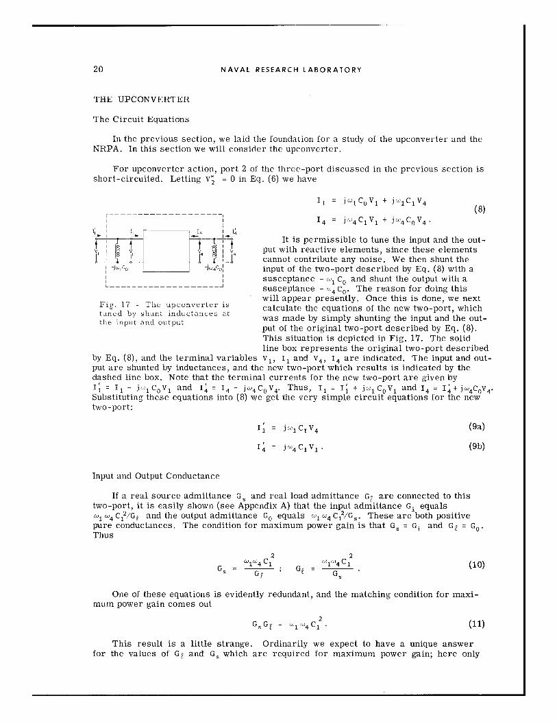
The Circuit Equations
In the previous section, we laid the foundation for a study of the upconverter and theNRPA. In this section we will consider the upconverter.
For upconverter action, port 2 of the three-port discussed in the previous section is
short-circuited. Letting V = 0 in Eq. (6) we have
I1 = jwlC 0 V1 + jCIV4 (8)
14 = jw 4 C1 V 1 + jCo4 C 0 V 4 .
I 1 [4 I 4i I-
" - -- It is permissible to tune the input and the out-V1 , I put with reactive elements, since these elements
I vI cannot contribute any noise. We then shunt the' -J. C0 -Jw4C01 input of the two-port described by Eq. (8) with a
susceptance - w1 Co and shunt the output with asusceptance - c 4 C0 " The reason for doing this
eupconverter i will appear presently. Once this is done, we nextFig. 17 - The calculate the equations of the new two-port, whichtuned by shunt inductances atthe input and output was made by simply shunting the input and the out-put of the original two-port described by Eq. (8).
This situation is depicted in Fig. 17. The solidline box represents the original two-port described
by Eq. (8), and the terminal variables V 1, i1 and V4 , 14 are indicated. The input and out-put are shunted by inductances, and the new two-port which results is indicated by thedashed line box. Note that the terminal currents for the new two-port are given by
1= I - j"'lcoV1 and 14 14 - j- 4 CoV 4 . Thus, I= I1 + i J 1 CoV 1 and 14 =I+ ji 4CoV 4.Substituting these equations into (8) we get the very simple circuit equations for the newtwo-port:
iI = j'lClV 4 (9a)
II = j- 4 C1 V 1 . (9b)
Input and Output Conductance
If a real source admittance Gs and real load admittance Ge are connected to thistwo-port, it is easily shown (see Appendix A) that the input admittance G, equalsco 14 C 2 /G and the output admittance Go equals -1 c04 C1 /G,. These are both positivepure conductances. The condition for maximum power gain is that G, = Gi and Ge = Go*Thus
2 2G 1'4 CW Ge 1 64 C1 (10)
Gg Gs
One of these equations is evidently redundant, and the matching condition for maxi-mum power gain comes out
2GsG F = w1 -w4C1 •( 1
This result is a little strange. Ordinarily we expect to have a unique answerfor the values of Ge and G, which are required for maximum power gain; here only
20
NAVAL RESEARCH LABORATORY 21
r"
the product of Ge and G, is fixed. This result comes about because the coefficients inEq. (9) are pure imaginary.
Gain
We next want to calculate the maximum available gain Am, which is defined as theratio of the power delivered to the load to the power delivered to the input when matchedconditions exist. Assume that matched conditions do exist. Then V1 and 1I are inphase, and v4 and I' are in phase (remember both the, input and output admittance arepure real); therefore, the input power is I•V1 and the power delivered to the load is I4V4.Multiply Eq. (9a) by I4 and (9b) by i i and equate the two. We then have
jIVl' 4 c 1 JIV 4vwlCi
I 4 V 4 A W4 f4__ Am -- _-
That is, the maximum available gain obtainable from an upconverter is the ratio of theoutput frequency to the input frequency.
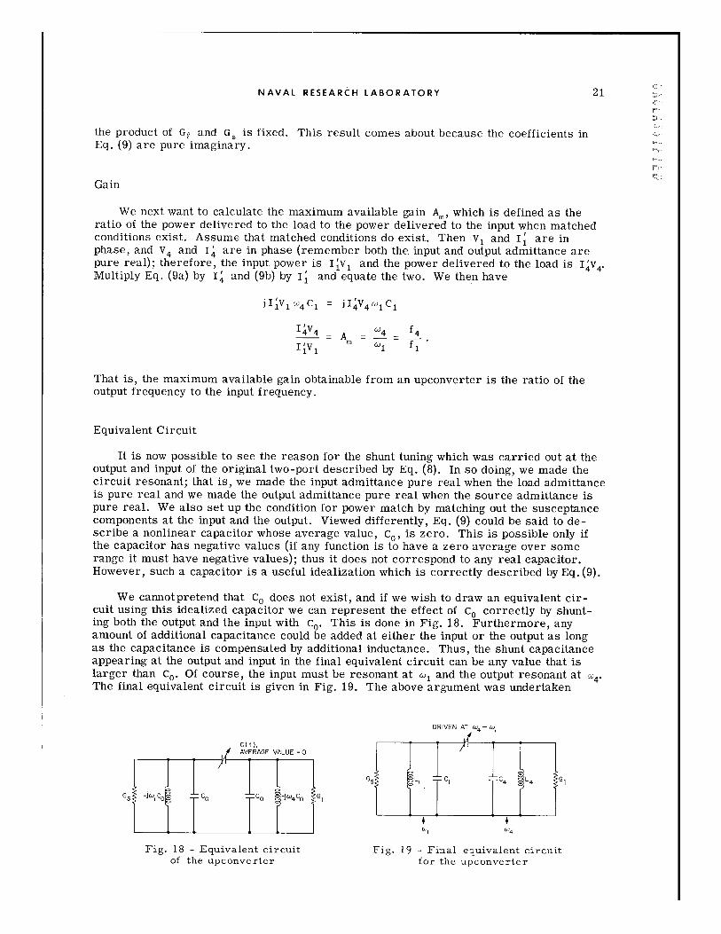
Equivalent Circuit
It is now possible to see the reason for the shunt tuning which was carried out at theoutput and input of the original two-port described by Eq. (8). In so doing, we made thecircuit resonant; that is, we made the input admittance pure real when the load admittanceis pure real and we made the output admittance pure real when the source admittance ispure real. We also set up the condition for power match by matching out the susceptancecomponents at the input and the output. Viewed differently, Eq. (9) could be said to de-scribe a nonlinear capacitor whose average value, C0 , is zero. This is possible only ifthe capacitor has negative values (if any function is to have a zero average over somerange it must have negative values); thus it does not correspond to any real capacitor.However, such a capacitor is a useful idealization which is correctly described by Eq. (9).
We cannot pretend that Co does not exist, and if we wish to draw an equivalent cir-cuit using this idealized capacitor we can represent the effect of Co correctly by shunt-ing both the output and the input with Co. This is done in Fig. 18. Furthermore, anyamount of additional capacitance could be added at either the input or the output as longas the capacitance is compensated by additional inductance. Thus, the shunt capacitanceappearing at the output and input in the final equivalent circuit can be any value that islarger than C0 . Of course, the input must be resonant at w1 and the output resonant at &)4.The final equivalent circuit is given in Fig. 19. The above argument was undertaken
C( t),AVERAGE VALUE = 0
C", W4
Fig. 19 - Final equivalent circuitfor the upconverter
Fig. 18 - Equivalent circuitof the upconverter

NAVAL RESEARCH LABORATORY22
because the circuit of Fig. 19 is often seen in the literature and is in fact sometimes thestarting point for the treatment of parametric amplification.
Noise Figure
From an intuitive point of view, it appears that all pure capacitors should be noise-less, whether they are linear or nonlinear. Experimental evidence indicates that this isthe case, although some theoretical work indicates that a very small amount of noise canbe expected from a pn junction capacitance. We will assume that the pn junction capac-itance is noiseless. Then the calculation of the noise figure of the upconverter becomestrivial. There is no source of noise in the upconverter, and therefore, it must have anoise figure equal to one for any source admittance. Incidentally, the same argumentholds for any network made up of capacitances and inductances-the noise figure alwaysequals one.
When we include the effect of the spreading resistance (which is a source of noise)the noise figure of the upconverter will be greater than one.
Bandwidth
In the section on the NRPA an expression will be derived for the gain-bandwidth.The gain-bandwidth calculation for the upconverter is similar, but since the algebra ismore complicated it will be omitted, and only the result will be given (2b). The maxi-mum possible bandwidth under high gain conditions is 2/Q1 , where Q1 is the Q of theinput tank circuit as loaded by G, and any losses present. In other words, the bandwidthof the upconverter is twice the bandwidth of the input tank. This may seem strange, butit is caused by the fact that the input conductance is a pure real positive number andtends to reduce the overall Q. We might expect Q4 , the Q of the output tank circuit, toappear in the expression for bandwidth. In fact, in an exact calculation Q4 does appear,but we are using an approximation which permits Q4 to be omitted.
The alert reader may ask what the practical value of the above formula for band-width may be. No criterion seems to exist for determining how low a value Q1 can have.The Q of the circuit, after all, can be made as low as is desired. A complete answer tothis question cannot be given until we consider the effects of the spreading resistance,but a partial answer can be given now. We are looking for some logical reason whichwould prevent one from making Q1 indefinitely small. The main loss in the input tankwhich controls Q1 is the source conductance G.. Equation (11) tells us what values ofG, are needed for high gain. If the value of G. is large then Ge will be small. But thiswill force the value of Q4 to be large, and if Q4 is too large the output tank is going tostart to limit the bandwidth.
This argument is not a quantitative one, but at least it indicates there is some limiton how small we can make Q1 . Nevertheless, in practice low values of Q1 are allowed,and the result is that the single-tuned upconverter, particularly when compared with thesingle-tuned NRPA is a broadband device.
PROPERTIES OF NEGATIVE RESISTANCE AMPLIFIERS
Introduction
The maser, the tunnel diode amplifier, and the negative resistance parametric am-plifier are (in their simplest forms) basically negative resistance amplifiers. At reso-nance, the equivalent circuit of these three devices is simply a noisy negative resistance
NAVAL RESEARCH LABORATORY 23
(or conductance). The particular value of the negative resistance and the noise temper-ature depends on the detailed physics of the device. Therefore, it seems reasonable totreat the general negative resistance amplifier (at resonance) so that the results may beapplied to any of the above three negative resistance amplifiers or to any new negativeresistance amplifiers which may be developed. It should be emphasized that this treat-ment applies only at resonance or at the center frequency of the device. This treatment,then, can yield no information concerning bandwidth.
Transducer Gain and Stability
The circuit for the simplest negative resistance amplifier at resonance is shown inFig. 20. The source on the left has a conductance G, and a short circuit current i,.On the right is shown a load of conductance Ge and in the middle is the negative conduct-ance of value -G. (Note that G is a positive number.)
Fig. 20 - Circuit for analyz-ing a negative conductance 1s GS G1amplifier
We will first consider the possibility of oscillations in this circuit, assuming that itis shunt resonant. It can be shown that a shunt resonant circuit will oscillate if the totalshunt conductance is less than or equal to zero. For this circuit to be stable we candemand that Gg + Gs - G > 0. This suggests defining a stability factor S = GC/G+ Gs/G- 1.The system is then stable if S > 0; and the larger S is, the more stable is the circuit.If S is nearly equal to zero, a small decrease in either Ge, G. or a small increase in G
will cause the circuit to oscillate.
The transducer gain AT is defined as the ratio of the power delivered to the load tothe power available from the generator. It is one of the more important parameters ofany power amplifier. For the circuit of Fig. 20 it can be shown that
4GgGs 4(Gp/G)(Gs/G) 4(Gg/G)(Gs/G)T (Ge + Gs - G) 2 (Ge/G + Gs/G - 1)2 S2
The expression on the far right indicates that the actual values of conductance are notimportant but that the conductive ratios are decisive.
The point of view taken here is that G is a parameter over which the engineer haslittle or no control. However, by means of transformers the engineer can control bothG. and Gg. No matter what the value of G, he can control the ratios Ge/G and Gs/G andthus can control S and AT. As a matter of fact, all the quantities of interest at the reso-nant frequency depend only on these or similar ratios, never on actual values.
We notice that according to Eq. (12), the condition S -* 0 (from the positive side),which is the condition for oscillations, is also the condition for large transducer gain.In fact, oscillations will start when the transducer gain approaches infinity. The abovefacts are the basis for the often seen statement that NRPA's, and in fact any NRA, areunstable. This behavior is sharply different from the behavior of ordinary (e.g., neu-tralized triode) amplifiers. If we consider the transducer gain of ordinary amplifiers asa function of G. and G2 we find that there are special values of each yielding a maximum

NAVAL RESEARCH LABORATORY
gain (the matched condition) which is not infinity. Of course, there are no terminal con-ditions which cause oscillations.
Available Gain and Noise Figure
We should be careful, however, not to overemphasize the importance of the trans-ducer gain for the following reason: In practice, negative resistance amplifiers arenearly always used as low-noise preamplifiers which feed conventional amplifiers, and
these, not the NRA, feed the final load. Furthermore, the parameter which is most im-portant is the overall amplifier noise figure. If the overall noise figure is satisfactory,then the transducer gain of the preamplifier (i.e., the NRA) is of little interest. If the
overall transducer gain is not high enough, it can always be increased by adding a fewfinal stages; this will not affect the noise figure. It is convenient to think of the overall
amplifier as a tandem connection of the preamplifier and a very high gain conventional
amplifier. Then the overall noise figure F is given by the tandem formula (Eq. (5)),where F1 and A1 refer to the preamplifier and F 2 refers to the conventional amplifier.Naturally, there is no point in using the preamplifier unless F is less than F 2 .
We next consider A1 and F 1 , and to investigate thelatter quantity we must make G noisy. Since G is inreality a two-terminal network, we can do this by plac-ing a short-circuit noise generator i1, of Fig. 21,
2 G2 across G. Let us calculate F 1 with aid of Fig. 21.From the definition of noise figure we see that i 2 is
Sn
given by 4kToG,. We might expect some difficulty be-cause -G is negative, but it is useful to simply definethe noise temperature of the negative conductance from
Fig. 21 - Noisy negative the equation i_ = 4kTG. The network of Fig. 21 is theconductance with noisy dual of the network of Fig. 4; thus, we arrive at thesource conductance proper expression for noise figure by replacing the
resistances by the conductances. (The negative signjust does not enter.) It is convenient to call the quan-
tity T/T 0 the noise temperature ratio of G. Let t T T/T 0 . The number t tells how manytimes hotter a two-terminal network is than room temperature. The expression for F 1
then becomes
G,F 1 = 1+tG- ' (13)
To calculate A1, which is the ratio of the available output power to the availablesource power, refer to Fig. 20. Assume that G. is always greater than G. We get
.2is2
4(G, - G) G1A1 = (14)1 2 G, G
S
4Gs
We see that if G becomes larger than G., the available gain becomes negative. Thereis, in fact, a way of handling this possibility, but for the sake of simplicity we will onlyconsider the case G < G.. Note that G. - G is really the output conductance, and we wouldexpect difficulty when this expression is negative.
The observant reader may note that according to Eq. (13) F 1 approaches to 1 as Gsapproaches infinity. This is really a trap, because Eq. (14) shows that, for the same
24
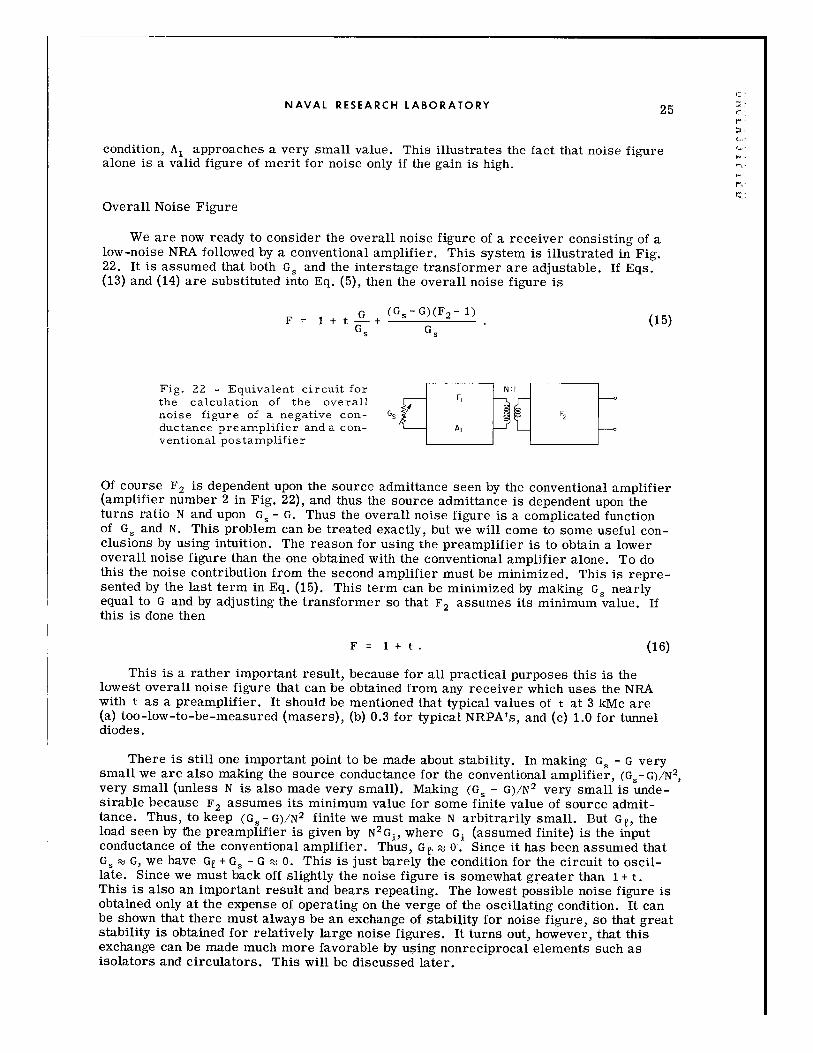
NAVAL RESEARCH LABORATORY 25
condition, A. approaches a very small value. This illustrates the fact that noise figure C'
alone is a valid figure of merit for noise only if the gain is high.
Overall Noise Figure
We are now ready to consider the overall noise figure of a receiver consisting of alow-noise NRA followed by a conventional amplifier. This system is illustrated in Fig.22. It is assumed that both G. and the interstage transformer are adjustable. If Eqs.(13) and (14) are substituted into Eq. (5), then the overall noise figure is
F(G-G)(f2- 1)Gs Gs
Fig. 22 - Equivalent circuit for N: I
the calculation of the overall F,
noise figure of a negative con- Gs F2
ductance preamplifier and a con- Aventional postamplifier
Of course F 2 is dependent upon the source admittance seen by the conventional amplifier(amplifier number 2 in Fig. 22), and thus the source admittance is dependent upon theturns ratio N and upon Gs - G. Thus the overall noise figure is a complicated functionof G. and N. This problem can be treated exactly, but we will come to some useful con-clusions by using intuition. The reason for using the preamplifier is to obtain a loweroverall noise figure than the one obtained with the conventional amplifier alone. To dothis the noise contribution from the second amplifier must be minimized. This is repre-sented by the last term in Eq. (15). This term can be minimized by making G, nearlyequal to G and by adjusting the transformer so that F 2 assumes its minimum value. Ifthis is done then
F = 1 + t. (16)
This is a rather important result, because for all practical purposes this is thelowest overall noise figure that can be obtained from any receiver which uses the NRAwith t as a preamplifier. It should be mentioned that typical values of t at 3 kMc are(a) too-low-to-be-measured (masers), (b) 0.3 for typical NRPA's, and (c) 1.0 for tunneldiodes.
There is still one important point to be made about stability. In making G, - G verysmall we are also making the source conductance for the conventional amplifier, (Gs-G)/N 2,very small (unless N is also made very small). Making (G. - G)/N 2 very small is unde-sirable because F 2 assumes its minimum value for some finite value of source admit-tance. Thus, to keep (G, - G)/N 2 finite we must make N arbitrarily small. But Gf, theload seen by the preamplifier is given by N 2 Gi, where Gi (assumed finite) is the inputconductance of the conventional amplifier. Thus, G g. ; 0. Since it has been assumed thatGr _ G, we have Ge + G. - G , 0. This is just barely the condition for the circuit to oscil-late. Since we must back off slightly the noise figure is somewhat greater than 1 + t.This is also an important result and bears repeating. The lowest possible noise figure isobtained only at the expense of operating on the verge of the oscillating condition. It canbe shown that there must always be an exchange of stability for noise figure, so that greatstability is obtained for relatively large noise figures. It turns out, however, that thisexchange can be made much more favorable by using nonreciprocal elements such asisolators and circulators. This will be discussed later.

NAVAL RESEARCH LABORATORY26
THE NEGATIVE RESISTANCE PARAMETRIC AMPLIFIER
Circuit Equations
A better name for the negative resistance parametric amplifier would be the nega-tive conductance parametric amplifier, but the former term is so well established in theliterature that we will use it.
To get NRPA action, port 4 of Fig. 16 is short-circuited. In Eq. (6) let V 4 = 0. Wehave
1 1 = jWICOV 1 + jw01 C 1 V2(17)
12 = - jiW2 C1 V 1 - jw)2 COV.2
We shunt-tune port 1 and port 2 exactly the same way and for exactly the same rea-sons as we did for the upconverter. The identical arguments apply, and the equations forthe new two-port (i.e., the two-port with tuning) are
Ii = + jwOlvC1 2
(18)(I*2)' z -jC02ClVl ,
where the primes indicate that the terminal currents of the new two-port are differentfrom the terminal currents of the original two-port.
Conductance Calculations
Proceeding as we did with the upconverter, the next task is to calculate the admit-tance looking into port 1 when port 2 is terminated with a conductance and vice versa.We want to be careful not to call one port the input port and the other port the outputport, because the NRPA is not used in this manner. Let us connect a conductance G2 onport 2 and calculate the admittance looking into port 1. Call this admittance Yi = G6 i + jBli"
This calculation is done just as it was for the upconverter (Eq. (10)) and the result is
2Y1 i = Gli = -' 'i 2 C1 /G 2 • (19)
This is an important equation. It says that at resonance a pure negative conductance ap-pears at port 1. Similarly, if we connect a conductance G1 on port 1 and calculate theadmittance looking into port 2, Y2 i, we will get
V2i = G2i = -" 1 2J2 C2/G1 • (20)
This can, in fact, be written down immediately from symmetry consideration.
Note that both Eqs. (19) and (20) demand that a finite conductance be connected to oneport if a finite negative conductance is to be observed at the other port.
Noise in the Negative Resistance Parametric Amplifier
According to Eqs. (19) and (20), a negative conductance can be produced at port 1 ofthe two-port described by Eq. (18) as long as a pure conductance is placed across port 2,and vice versa. It is customary to call the port at which the negative conductance is pro-duced the signal port and to call the other port the idler. It is not clear at this point

NAVAL RESEARCH LABORATORY 27
which port should be chosen as the signal port, but we shall start by picking port 1, whichcorresponds to the lower frequency. , .
An equivalent circuit for this amplifier, including source and load is shown in Fig.23. Here GI, which was formerly called G2, is the idler load. This figure should becompared with Fig. 20. Note that there are three distinct conductances which we mustconsider: the source conductance G,, the load conductance Gf, and the idler conductanceGI. In addition, of course, the negative conductance of port 1 is shunted across the sourceand load just as in Fig. 20. This negative conductance (G6i in Eq. (19)) will now simplybe -G (just as in Fig. 20).
G,
Fig. 23 - Equivalent circuitof the NRPA PORT I
The noise figure and available gain of this amplifier have already been worked outand are given in Eqs. (13) and (14). In addition, the minimum possible overall noise fig-ure obtainable using this amplifier as a preamplifier has been given in Eq. (16). Oneproblem remains, however: What is the noise temperature ratio looking into port 1 ?
Port 1 must be noisy. We know that GI must have a finite value; thus if G6 is at afinite temperature T1 there will be thermal noise at the terminals of GJ. This noise isat the idler frequency, but because of the mixing process, this noise will appear at thesignal port and produce a noise temperature ratio, t. We can calculate t as follows.The thermal noise of G6 can be represented by a short-circuit noise generator i1 , where12 = 4kTI GI . Then we ask the following question: If port 2 is driven by a generator of
source conductance GI and short-circuit current iI, what short-circuit noise current i,,is produced at port 1 ? This is a straightforward circuit problem. Once in is deter-mined, the noise temperature at port 1 is given from i 2 = 4kTG, and thus t = in2/(4kGT 0 ).But we have already calculated G (Eq. (19)); thus
t T= l (20)
Let w•s 61, __ W2, and TI/T 0 = t 1 . Then
t = tI 2
where t, is the noise temperature ratio of Gi. It is customary to call co and &)I thesignal and idler frequencies respectively. It will be recalled that C02 is greater than cc,and therefore t is less than tI. In fact, by making the ratio of the idler frequency to the

NAVAL RESEARCH LABORATORY
signal frequency become arbitrarily large, t can be made arbitrarily close to zero.Another way of saying this is that the downconversion process from W2 to c 1 is an inef-ficient process; thus noise originating at frequency W2 is reduced when it appears at fre-quency wl. Had we picked port 2 as the signal port and port 1 as the idler port, the ratiowould have gone the other way; that is, t would be given by ti(w2/W1 ) and the idler noisewould be magnified in the conversion process. For this reason, the idler frequency isnever made less than the signal frequency, and if possible, the idler frequency is madevery large compared with the signal frequency.
According to (Eq. 20), cooling GI will reduce ti. This is done in some practicalamplifiers.
If Eq. (20) is substituted into Eq. (16) we have for the lowest possible overall noisefigure using a NRPA as a preamplifier
F = 1 + ti(fsfi). (22)
As an example, consider a NRPA operating at 200 Mc with the idler at room tem-perature at 1000 Mc. Then the minimum noise figure would be 1.2. In practice, theidler circuit is often a resonant cavity and Gi may simply consist of the cavity losses.Then the idler noise temperature ratio is just the noise temperature ratio of the cavity,or Tc/T 0, where T, is the cavity temperature.
Bandwidth
Up to now, we have only been considering the center or resonant frequency proper-ties of the NRPA. The algebra was relatively simple because everything was pure realat the center frequency. It is important to know (for any amplifier) how the properties ofthe amplifier change as the input frequency deviates from the center frequency. In par-ticular, we are usually interested in the frequency dependence of the transducer gain AT.
The center frequency value is given by Eq. (12). Normally, one is not interested in ATat frequencies far removed from the center frequency because AT would simply be verysmall and not useful. Therefore, we seek an expression for the transducer gain for fre-quencies close to the center frequency. Naturally, expressions of the form G + j(WC- 1/wL)
will frequently appear in such calculations.Viewed as a function of 6, the above is a rather
G, unwieldy expression. It is well known that for
RESONANT frequencies close to resonance this expressionAT n2 can be written as G(1 + j2 SQ), where 8 is the
fractional deviation of the signal frequencyfrom the resonant frequency w0. Thus,6 = (a--o)/co,, and Q is given by G/o c. Thisexpression simplifies things, because it is
IY linearly dependent upon frequency in contrastto the original expression.
The equivalent circuit for the bandwidthcalculation is shown in Fig. 24. This looksIs GS G like Fig. 23, except that signal and idler tanks
tuned to frequencies f2l and f22 are indicated.Note that the admittance looking into the signal
RESONANTAT nI port not including the signal tank is called Y.
The actual signal and idler frequencies, which
Fig. 24 - Equivalent circuit for are now assumed to differ from Q1 and f22, arecalculation of the bandwidth of designated by w, and w2. The load current isthe NRPA given by
28

NAVAL RESEARCH LABORATORY 29C"
e de + Y + Y
where Y 1 is the sum of G, and the signal tank circuit. Then the power delivered to theload is
Pe if'1 Ge 2
JGe + YI + Y, 2
and the power available from the source is
4G s
The frequency dependent transducer gain AT. is by definition PF/Ps, and thus we have
4Gg G;AT • = Ge + Y 1 + Y, 2 (23)
Clearly, the frequency dependence of AT. is to be found in Y and YX"
The details (3) of the calculation will not be given here, but the bandwidth is obtainedby setting the denominator (since the numerator is frequency independent) equal to twiceits center frequency value and solving for frequency. The result is
Gs+Gg-G (426' = GS + G2 - (24)Q, [G. + GeC + (Gf~lQ2Q2 Q0Q1]
where 6' is that particular value of (w- 2i)/ 1 = ý at which the transducer gain hasdropped to half its center frequency value, Q, is the total Q of the signal tank (i.e., itincludes G. as well as any losses in the resonant circuit), and Q2 is the Q of the idlertank including all conductance shunting that tank except that seen looking into port 2.
Note that the numerator of this expression is the square root of the denominator ofthe expression for center frequency transducer gain which was given in Eq. (12). If Eq.(12) is solved for the quantity Gg + G5 - G and the result substituted into Eq. (24) we get
28 ST 2 2 QIGTI + QIQ 2 G (25)
where GT1 is the total conductance shunting the signal tank (but not including G); that is,it is G, + Ge, plus the losses associated with the signal tank, which are usually smallwhen compared with G + G
Since Eq. (25) involves the square root of the transducer power gain and since volt-age is proportional to the square root of power, Eq. (25) is often called the gain-bandwidthin analogy to low frequency definition. Usually the Q of the idler tank is large when com-pared with the Q of the signal tank because the signal tank must of necessity be loadedwith G, and Ge. Thus we can write
gain x bandwidth = 2 QQ2 iGsGp (26)?F Q2 YdGG

NAVAL RESEARCH LABORATORY
For large transducer gain, G + G G; thus
gain x bandwidth 0 2 1 ___s ss _-
Tý Q; (Z;s+G F KGs+F
2 02 1 ( 1 G gG s71 Q2 Gl ;G.G'
As a function of Gg/Gs, this expression is maximum when GF/G= 1, and for this casewe have the final answer for the maximum gain-bandwidth product:
gain x bandwidth = 1 02 (27)Q2 Q1
This is an important formula. It must be remembered that this formula refers tothe square root of the power gain and that the bandwidth is the fractional bandwidth.
Let us consider a simple problem using this formula: Is it feasible to build a low-noise NRPA at 400 Mc with an idler frequency at 4000 Mc, a gain of 20 db, and an abso-lute bandwidth of 0.5 Mc? The transducer power gain equals 100, and the square root ofthis is 10. A typical Q for a resonant circuit at 4000 Mc would be, say 1000. The frac-tional bandwidth then equals 10 3 which means that the absolute signal bandwidth wouldbe about 0.5 Mc. Thus, it would appear feasible to build such an amplifier.
Circulators, Isolators, and Negative Resistance Amplifiers
At microwave frequencies nonreciprocal circuit elements such as circulators andisolators are available and may be usefully employed with negative resistance amplifiers.
An isolator is a two-port device which passes microwaves with nearly zero loss inone direction and nearly infinite loss in the other direction. At port 1 a waveguide matchis seen regardless of what is connected to port 2, and looking in port 2 a match is seenregardless of what is connected to port 1. Isolators can be used with a negative resist-ance as is shown in Fig. 25.
Note that the apparent source and load conductances which are loading G, namely G,,and G' are nearly constant regardless of changes in G,, and Gg. Thus, this amplifier ismore stable against changes in G, and Gg than the amplifier of Fig. 20. Of course,changes in G are just as important as ever; thus these changes must be minimized by
holding the pump power constant and perhaps bystabilizing the diode temperature. There aretwo other points which should be mentioned:
GSG, First, we have now a separate input port andTh- output port and second, neither the output con-
ductance nor the input conductance will be neg-% G G ative regardless of the values of G. and Gp
I I (assuming that the isolator is perfect). The
IDEAL) other properties of the negative resistanceISOLATOR I TRANSFORMER ISOLATOR 2 amplifier such as bandwidth and noise figure
are unchanged.Fig. 25 - A combination of iso-lator and a negative conductance A circulator is a lossless three-port device.to produce a more stable low- It is best described in terms of waves. A wavenoise amplifier entering port 1 is transmitted without loss to
30
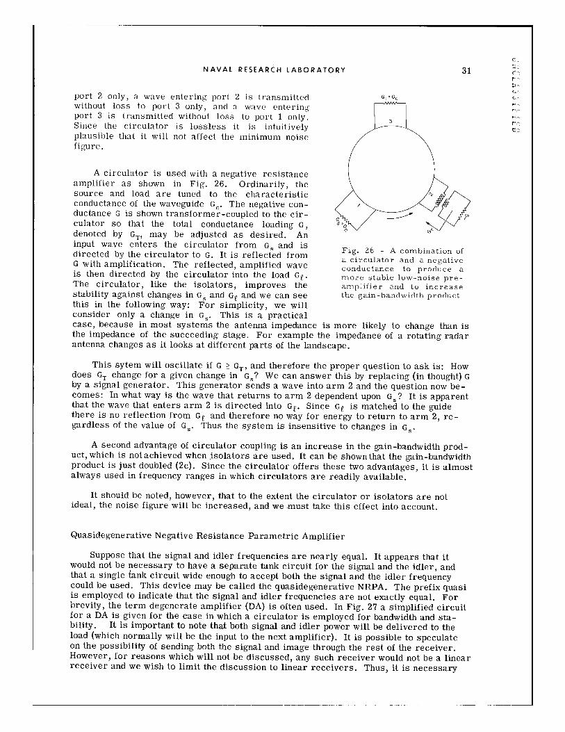
NAVAL RESEARCH LABORATORY
port 2 only, a wave entering port 2 is transmittedwithout loss to port 3 only, and a wave enteringport 3 is transmitted without loss to port 1 only.Since the circulator is lossless it is intuitivelyplausible that it will not affect the minimum noisefig-ure.
A circulator is used with a negative resistanceamplifier as shown in Fig. 26. Ordinarily, thesource and load are tuned to the characteristicconductance of the waveguide G,. The negative con-ductance G is shown transformer-coupled to the cir-culator so that the total conductance loading G,denoted by GT, may be adjusted as desired. Aninput wave enters the circulator from G, and is Fdirected by the circulator to G. It is reflected fromG with amplification. The reflected, amplified wave cois then directed by the circulator into the load Ge. mThe circulator, like the isolators, improves the astability against changes in G, and Gg and we can see ththis in the following way: For simplicity, we willconsider only a change in Gs. This is a practicalcase, because in most systems the antenna impedance is mothe impedance of the succeeding stage. For example the imiantenna changes as it looks at different parts of the landscape.
ig. 26 - A combination ofcirculator and a negativeinductance to produce aore stable low-noise pre-nplifier and to increasee gain-bandwidth product
-e likely to change than is)edance of a rotating radar
This sytem will oscillate if G > GT, and therefore the proper question to ask is: Howdoes GT change for a given change in G,,? We can answer this by replacing (in thought) Gby a signal generator. This generator sends a wave into arm 2 and the question now be-comes: In what way is the wave that returns to arm 2 dependent upon G.? It is apparentthat the wave that enters arm 2 is directed into Ge. Since Ge is matched to the guidethere is no reflection from Ge and therefore no way for energy to return to arm 2, re-gardless of the value of G,. Thus the system is insensitive to changes in G.
A second advantage of circulator coupling is an increase in the gain-bandwidth prod-uct, which is notachieved when isolators are used. It can be shown that the gain-bandwidthproduct is just doubled (2c). Since the circulator offers these two advantages, it is almostalways used in frequency ranges in which circulators are readily available.
It should be noted, however, that to the extent the circulator or isolators are notideal, the noise figure will be increased, and we must take this effect into account.
Quasidegenerative Negative Resistance Parametric Amplifier
Suppose that the signal and idler frequencies are nearly equal. It appears that itwould not be necessary to have a separate tank circuit for the signal and the idler, andthat a single iank circuit wide enough to accept both the signal and the idler frequencycould be used. This device may be called the quasidegenerative NRPA. The prefix quasiis employed to indicate that the signal and idler frequencies are not exactly equal. Forbrevity, the term degenerate amplifier (DA) is often used. In Fig. 27 a simplified circuitfor a DA is given for the case in which a circulator is employed for bandwidth and sta-bility. It is important to note that both signal and idler power will be delivered to theload (which normally will be the input to the next amplifier). It is possible to speculateon the possibility of sending both the signal and image through the rest of the receiver.However, for reasons which will not be discussed, any such receiver would not be a linearreceiver and we wish to limit the discussion to linear receivers. Thus, it is necessary
I-.
4,,
C,
31
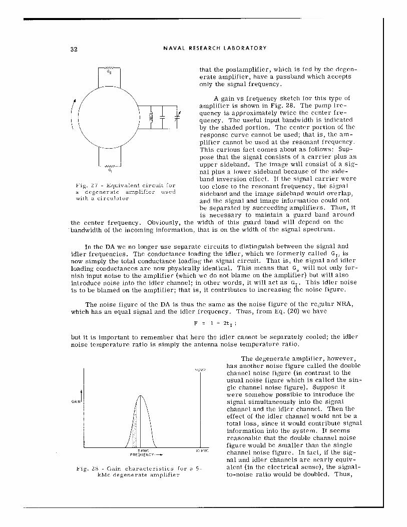
NAVAL RESEARCH LABORATORY
- that the postamplifier, which is fed by the degen-erate amplifier, have a passband which acceptsonly the signal frequency.
A gain vs frequency sketch for this type ofamplifier is shown in Fig. 28. The pump fre-quency is approximately twice the center fre-
7 quency. The useful input bandwidth is indicated- by the shaded portion. The center portion of the
response curve cannot be used; that is, the am-plifier cannot be used at the resonant frequency.This curious fact comes about as follows: Sup-pose that the signal consists of a carrier plus anupper sideband. The image will consist of a sig-nal plus a lower sideband because of the side-band inversion effect. If the signal carrier were
Fig. 27 - Equivalent circuit for too close to the resonant frequency, the signala degenerate amplifier used sideband and the image sideband would overlap,with a circulator and the signal and image information could not
be separated by succeeding amplifiers. Thus, itis necessary to maintain a guard band around
the center frequency. Obviously, the width of this guard band will depend on the
bandwidth of the incoming information, that is on the width of the signal spectrum.
In the DA we no longer use separate circuits to distinguish between the signal andidler frequencies. The conductance loading the idler, which we formerly called GI, isnow simply the total conductance loading the signal circuit. That is, the signal and idlerloading conductances are now physically identical. This means that G. will not only fur-nish input noise to the amplifier (which we do not blame on the amplifier) but will alsointroduce noise into the idler channel; in other words, it will act as GI. This idler noiseis to be blamed on the amplifier; that is, it contributes to increasing the noise figure.
The noise figure of the DA is thus the same as the noise figure of the regular NRA,
which has an equal signal and the idler frequency. Thus, from Eq. (20) we have
F = 1 + 2t 1 ;
but it is important to remember that here the idler cannot be separately cooled; the idler
noise temperature ratio is simply the antenna noise temperature ratio.
The degenerate amplifier, however,has another noise figure called the doublechannel noise figure (in contrast to theusual noise figure which is called the sin-gle channel noise figure). Suppose itwere somehow possible to introduce the
GAIN signal simultaneously into the signalchannel and the idler channel. Then theeffect of the idler channel would not be atotal loss, since it would contribute signalinformation into the system. It seemsreasonable that the double channel noise
__ figure would be smaller than the single5 KMC 10KMC channel noise figure. In if the
FREQUENCY-e fact,nal and idler channels are nearly equiv-
Fig. 28 Gain characteristics for a 5- alent (in the electrical sense), the signal-kMc degenerate amplifier to-noise ratio would be doubled. Thus,
32
NAVAL RESEARCH LABORATORY 33
the noise figure would be halved; that is, the double channel noise figure would be 3 dbless than the single channel noise figure.
There is one very important application in which information is easily fed in bothchannels so that the double channel noise figure is appropriate. This was discussed inthe section on noise under the heading "The Extended White Noise Source" (p. 15). Herethe "signal" consists of a wideband noise source which is relatively frequency independ-ent. The amplitude of this noise represents the noise temperature of the astronomicalentity being studied. Since the source is so wideband, it is a simple matter to feed thisenergy into both channels-in fact, in the DA it would be difficult to avoid feeding it intoboth channels. It seems reasonable that the double channel noise figure should apply inthis case. If, for example, the spreading resistance were nearly zero; that is, if theparametric diode were nearly a pure capacitance, then there would be no noise from thediode and of course no idler noise-therefore a noise figure of zero db would be expected.
It does seem, however, that in the case of a radar type signal the single channel noisefigure would apply. It is difficult to conceive of a conventional radar signal which couldbe fed into both channels without the overlap of signal and idler sidebands mentionedpreviously.
The concepts of single and double channel noise figure are not new. They arise infact in any mixer. Consider for example, the con Tentional radar mixer. Suppose the i-fis 30 Mc and the local oscillator is operating at 10,030 Mc. Then there will actually betwo possible input channels, one at 10,000 Mc and one at 10,060 Mc. These frequenciesare close together as far as microwave circuitry is concerned, and unless microwavefilters are used (and they usually are not) impedances will be the same for both channels.That is, the two channels will be electrically equivalent. Normally, one of the channelsis not used but, of course, it contributes noise exactly analogous to idler noise. Such areceiver will exhibit a 3-db improvement in noise figure if it is used for the type ofastronomical observation we have been discussing.
Here is a quick review of the degenerate amplifier: The DA is a particular form ofthe NRPA in which the signal and idler frequency are both nearly equal to one-half thepump frequency and are both contained within the passband of one tuned circuit. Twokinds of noise figure are defined for this amplifier-the single-channel noise figure, -which applies to most cw type signals such as radar, communications, etc., and the dou-ble channel noise figure which is used when the "signal" consists of broadband noisefrom an object whose temperature is sought. The single channel noise figure is 3 dblarger than the double channel noise figure.
Broadbanding the Negative Resistance Parametric Amplifier
The theoretical bandwidths of the degenerate and nondegenerate NRPA are, of course,quite small and the experimental bandwidths are usually somewhat smaller even than thetheory predicts. A natural question arises as to whether these narrow bandwidths are anintrinsic property of NRPA's or whether they are caused by the fact that we have em-ployed simple single-tuned resonant circuits for sorting out the various frequencieswhich are involved in PA operation. In the final analysis a NRA will give gain at anyfrequency at which a negative resistance is present. Equation (19) indicates that in thecase of the NRPA the frequency dependence of the negative conductance is certainly notgreat enough to account for bandwidths of only a few percent. The frequency dependenceof the transducer gain is contained in the denominator of Eq. (23) in Y and Y1 , where Y isthe admittance of the input tank circuit and is strongly frequency dependent, as in anysingle tuned circuit. We have not given an expression for Y1, which is the admittancecoupled into the signal circuit from the idler circuit, but it can be shown that Y1 isstrongly frequency dependent, mostly because the idler circuit is also a single tuned circuit.

34 NAVAL RESEARCH LABORATORY
Thus it would appear that if bandpass filters, with their broader, more flat-topped
response, were used instead of the single-tuned circuits an increased bandwidth wouldresult. This reasoning is correct, and although the broadbanding of NRPA's by this meansis still in the early development stage, it has been shown both experimentally and theo-retically (4) that bandwidths of the order of 20 percent are feasible without significantsacrifice of the low noise properties.
Naturally, this procedure is simplest in the case of the DA because only one filter is
involved, and most of the early experimental broadband work was done on the DA. Thedesign procedure is at present rather complex, and a detailed analysis will not be given,but some experimental results will be given in a later section.
THE EFFECT OF SPREADING RESISTANCE
Introduction
In the section on parametric diodes, it was pointed out that all practical parametricdiodes have a spreading resistance R, in series with a nonlinear capacitance, and some
of the consequences of this fact were noted. It is to be expected that all the properties of
any type of PA will be affected by the spreading resistance for high enough frequencies.The gain, bandwidth, and noise figure will be different for finite R., and in addition, there
will be some new design considerations. For example, the pure nonlinear capacitor(Rs = 0 ) does not absorb pump power; when R is added, however, it will absorb pump
power proportional to the square of the pump frequency. This can be an important de-sign consideration.
In principle, it would be relatively easy to go over the calculations we made earlierand consider in detail the effect of a finite Rs. It is a relatively straightforward prob-lem in linear circuit theory. The calculations are rather involved, however, and only theresults are presented here.
Two parameters are important for describing the parametric diode when the effects
of spreading resistance are included. The first, Y, is nearly equal to C1 /Co. The quan-
tity y is essentially a measure of the degree of nonlinearity of the diode when driven bythe pump. If the pump drive is weak, y will be small, and as the pump drive is increased,
y will increase. Of course, the pump drive cannot be increased indefinitely or the diode
will be driven into conduction, so the maximum value of y is limited. A reasonable valueof y for an exceptionally good diode driven hard is 0.3; a typical value is 0.25.
The second parameter which is important in describing the parametric diode is thecutoff frequency o,. This is the frequency at which the spreading resistance is equal toi/(WC0) ; in other words, at w,, the impedance of the spreading resistance is equal to the
impedance of the fictitious capacitor C0 , where Co is just the average value of the diodecapacitance through the pump cycle. In calculations it is customary to define an effectiveQ at the lowest frequency &I as follows:
Q = 1/(w 1 C0 Ro) . (28)
Since by definition Co R. = icoc, we have
Q = W/Ci" (29)
Thus, if we know the cutoff frequency of a diode, we can always calculate the proper Q
corresponding to the frequency a). Note that if w, is large, which it will be if either R.is small or Co is small, Q will be large. We now discuss the detailed effect of these twoparameters on the properties of the upconverter and the NRPA.
NAVAL RESEARCH LABORATORY 35
The Upconverter C,
Transducer gain (2d) is given by
f4 XAT - f1 [1+ f-x] 2 (30)
where X = (f1 /f 4 )(/Q) 2 and f, = w 1 / 2,r.
From Eq. (30), we can obtain an upper bound for the gain by letting Q approachinfinity. It is easily seen that for this case, X approaches infinity and thus the gain ap-proaches f 4/f . This agrees with our treatment for R. equal to zero.
But we can derive a still more interesting result from Eq. (30). Suppose we have agiven diode being driven hard; that is, - and f are given. Suppose that the input fre-quency f 1 is also given. Assume that we are willing to make the pump frequency (andthe output frequency) as high as is necessary to reach the maximum gain. What is themaximum possible gain if we let f 4 /f 1 approach infinity ? Intuition tells us that the gainwill not approach infinity but will approach some finite value because the diode must,after all, operate at f 4 , and as f 4 becomes larger and larger, the diode becomes lessefficient because of the spreading resistance.
From Eq. (30) the gain (AT) becomes
(AT). = (1/4)(-/Q) 2 (31)
Remember that Q is defined at f 1 . Insofar as transducer gain is concerned, -Q is con-sidered to be a very important figure of merit for the diode because for a given inputfrequency it determines what the maximum gain can be.
Consider a practical problem: A diode with a cutoff frequency of 20 kMc andy = 0.25 is available for use in an upconverter of input frequency of 0.5 kMc. Whatis the maximum possible gain, and what is a reasonable pump frequency?
The Q is f c/f, which in this case equals 40; (-/Q) 2 equals 100; thus the maximumgain is 25. The gain equals 25 when f 4 is infinite, but Eq. (30) gives the gain for anyfinite value of f 4; therefore we can substitute tentative values of f4 into Eq. (30) untilthe gain is as close to 25 as desired.
Let us now consider bandwidth (2e). The fractional bandwidth for a high quality(high Q) diode is given by
2 -' = 2-/ -f4 /fl • (32)
This equation predicts very large bandwidths for the upconverter; in fact, for large f 4/fl,the predicted bandwidth is absurdly large. This is due to the failure of some of the as-sumptions of the derivation. We will simply conclude that very large bandwidths arepossible for the upconverter and that the bandwidth increases with an increase in y andf 4/fl. At present no simple method of predicting bandwidth exists.
Finally, we consider noise figure. Assuming that yQ >> 1, the noise figure for opti-mum source impedance is given by (2f)
FO = 1+ 2 tD (33)yQ

NAVAL RESEARCH LABORATORY
where tD is the noise temperature ratio of the spreading resistance. Good agreementwith experimental data has been obtained by assuming that tD is the ambient tempera-ture of the diode. As an example, suppose the diode is operated at room temperature and-Q = 10. Then the noise figure is approximately 1.2. Note that the quantity yQ againappears as a sort of figure of merit for a given input frequency.
The Negative Resistance Parametric Amplifier
Gain is not of great interest because it can always be made infinite for any negativeresistance amplifier. However, gain bandwidth (2 g) is of great interest and it is given by
26'(AT)1/2 - 2(8) (234
This formula applies to the case in which a circulator is not used. As an example,suppose that the gain is 20 db, y is 0.25, and the idler frequency is four times the signalfrequency. The maximum possible bandwidth will then be about 2.5 percent.
We next shall consider the noise temperature ratio t of the NRPA when R. is finite.The general solution is too complicated to be of much value to us, but there is one ratherpractical special case which gives simple results. If we assume that the losses in theidler circuit are small compared with R,,, then the expression for t becomes*
K2 (72 +1~
t = tD K2Q2-1 (35)On -- 1
where tD is the noise temperature of Rs; K = yQ and 0 =•ýIw". It is natural to supposethat tD is simply the ambient temperature of the diode. This assumption does seem toagree with the experimental evidence; that is to say, cooling the diode does lower t pro-vided that the diode will continue to operate properly at the reduced temperature.
We note that -Q appears again as a figure of merit for the diode. For a given diodeoperated at a given temperature and signal frequency, t0 and K are fixed. The designerstill has freedom however, in choosing the idler frequency (i.e., in choosing Q).
It is clear, that unlike the case for R. = 0, the optimum idler frequency is not infi-nite. In fact, it appears that there is a finite value of the idler frequency which will givethe minimum value for t. This can be found by the usual method; that is, by taking thederivative of Eq. (35) with respect to £ and setting it equal to zero. Assuming that K ismuch greater than one, we have for the optimum value of Q
1- =-1 . (36)op 'YQ
The optimum value of Q can in turn be substituted back into Eq. (35), thus giving usthe optimum value of t
t - 2tD (37)op •
*Equation (35) can be deduced from Knechtli's Eq. (40) with /t - 0 (small idler circuit
losses) and a = I (high gain) along with Eq. (41), which permits elimination of p-t. This
procedure is permissible because my t is identical with Knechtli's tni, even though thelatter describes a four-terminal amplifier. See Ref. 5.
36
NAVAL RESEARCH LABORATORY
Finally, when the optimum value of t is substituted into Eq. (16) it will yield anexpression for the optimum or lowest noise figure:
FoP = 1+ 2 t- (38)YQ
In practice, it may not always be feasible to use the optimum idler frequency, be-cause the pump frequency required may be in a difficult frequency range. In this case,one can tentatively choose an idler frequency which does give a convenient pump frequency.The noise temperature ratio for this idler frequency can be computed from Eq. (35) andcompared with the lowest possible value given by Eq. (37), and thus the penalty for notusing the optimum idler frequency can be adjudged to be either acceptable or not accept-able. This procedure can be repeated until an acceptable solution is obtained.
Equation (38) is one of the most important equations of NRPA theory. We will use itto estimate the noise figures expected from the best NRPA's. At present commerciallyavailable varactor diodes have cutoff frequencies up to about 200 kMc. If we assume thattD equals 0.25 (liquid nitrogen temperature) and y equals 0.25, then at X-band a 200-kMc-diode will have an F0 p equal to 1.1. There are very few systems that require alower noise figure.
Pump Power
Since pump current must flow through the spreading resistance, pump power P isdissipated in the spreading resistance. By making two simplifying assumptions, wePcanestimate what the pump power must be. First, assume that the pump voltage which ap-pears across the diode terminals is sinusoidal, and second, assume that the diode isbiased halfway between zero and breakdown voltage vB. A large y is always desirable,and clearly - has its largest value if the pump voltage amplitude is equal to V,/2. Then,the voltage across the spreading resistance V. is
v = 2 [-- - Rs - /(•sCo)) ,
where &)3 is the pump frequency. Since the capacitance varies throughout the pump cy'cle,it is not clear what value of capacitance should be substituted into the above formula, butCo appears to be a good approximation. At any rate we expect only a rough estimate.The power dissipated in R, is jV\I 2/(2R,); thus
2 2VB 1RsP 4 2 22
(Rs + 1/W 2 C0o) 2R.
2VB R s
8 2 2 2Rs + 1/cv3 CO
Divide the numerator and denominator by R,, and recall that the cutoff angular frequencyw, is given by 1/CoRs. We have
2VB 1/Rs
P 8 2 21 + fc/f3
37
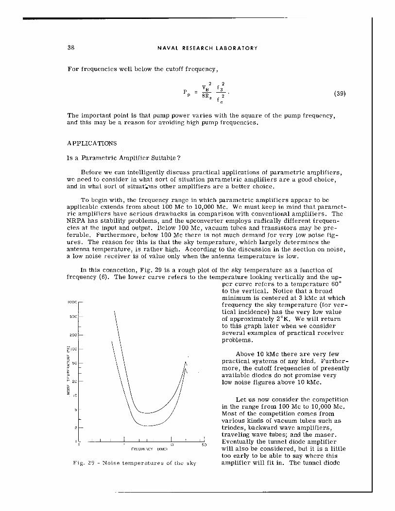
NAVAL RESEARCH LABORATORY
For frequencies well below the cutoff frequency,
2 2VB f 3 (39)
The important point is that pump power varies with the square of the pump frequency,and this may be a reason for avoiding high pump frequencies.
APPLICATIONS
Is a Parametric Amplifier Suitable?
Before we can intelligently discuss practical applications of parametric amplifiers,we need to consider in what sort of situation parametric amplifiers are a good choice,and in what sort of situatk-ns other amplifiers are a better choice.
To begin with, the frequency range in which parametric amplifiers appear to beapplicable extends from about 100 Mc to 10,000 Mc. We must keep in mind that paramet-ric amplifiers have serious drawbacks in comparison with conventional amplifiers. TheNRPA has stability problems, and the upconverter employs radically different frequen-cies at the input and output. Below 100 Mc, vacuum tubes and transistors may be pre-ferable. Furthermore, below 100 Mc there is not much demand for very low noise fig-ures. The reason for this is that the sky temperature, which largely determines theantenna temperature, is rather high. According to the discussion in the section on noise,a low noise receiver is of value only when the antenna temperature is low.
In this connection, Fig. 29 is a rough plot of the sky temperature as a function offrequency (6). The lower curve refers to the temperature looking vertically and the up-
per curve refers to a temperature 600to the vertical. Notice that a broadminimum is centered at 3 kMc at which
1000 -frequency the sky temperature (for ver-tical incidence) has the very low value
500 of approximately 2'K. We will return
to this graph later when we consider
200 several examples of practical receiverproblems.
1 00
Above 10 kMc there are very fewS50 practical systems of any kind. Further-
more, the cutoff frequencies of presentlyavailable diodes do not promise very
20 low noise figures above 10 kMc.
to-Let us now consider the competition
5 - in the range from 100 Mc to 10,000 Mc.Most of the competition comes fromvarious kinds of vacuum tubes such as
2 triodes, backward wave amplifiers,traveling wave tubes; and the maser.
r I 50 q Eventually the tunnel diode amplifier1 0 50FREQUENCY (KMC) will also be considered, but it is a little
too early to be able to say where thisFig. 29 - Noise temperatures of the sky amplifier will fit in. The tunnel diode
38
NAVAL RESEARCH LABORATORY 39
amplifier has stability problems just like the NRPA. It can be extremely simple andlightweight, and its noise figure is similar to that of the vacuum tube.
Generalizations are risky, but it appears that in the frequency range in which we areinterested, the maser is the quietest, the vacuum tube is the noisiest and the parametricamplifier falls between the two. At 3 kMc, typical values for the three amplifiers are:the maser, almost too low to measure; the PA, 1.5 db; the vacuum tube, 3 db.
However, with respect to bandwidth, the vacuum tube (traveling wave tube) rates thehighest, the PA next, and the maser last.
With respect to simplicity, the tube would seem to rate highest (no pump, no extra-neous frequencies to deal with), the PA next, and the maser a very poor last, since bothvery low temperatures and a magnet are required.
At this time we are not attempting to consider which type of PA would be optimumbut only to choose between tubes, masers, and PA's. The three following examples mightbe helpful:
1. A receiver is to be designed for a scatter communications system in a large landbased installation. The narrow beam antenna is to be at an angle of about 300 to the hori-zontal. The center frequency is to be 3000 Mc and the bandwidth is to be 50 kc. Thestability requirements are modest. What type of amplifier should be used? Referring toFig. 29 we see that we are going to have a very low antenna temperature. Equation (3) isapplicable here and indicates that when the antenna temperature T is very low, a verylow noise figure receiver should be used. Thus, the maser is suggested, and in a largeland-based installation we could handle the weight, cost, and complexity of the maser.
2. A receiver is required for an airborne search radar. The antenna temperatureis about 200'K, and the frequency is 1000 Mc. What type of amplifier should be used?The antenna temperature is considerably higher here-in fact, too high to make the maser,with its weight and complexity, at all attractive. At the same time, modest bandwidthsare usually acceptable in search radars, and Eq. (3) indicates that a lower noise figurethan that usually obtainable from tubes would appreciably increase the sensitivity. Sometype of PA is indicated.
3. A short range X-band tracking radar receiver is needed for a system in whichvery accurate range information is desired. The antenna temperature is near room tem-perature. What type of amplifier should be used? For good range resolution an ordinaryradar system needs fast rise time pulses. This, in turn, means large rf bandwidth. Al-though the outlook for broadband PA's is good, they are still in the experimental stage.Furthermore, since the antenna temperature is rather high, we can accept the largernoise figure of tubes. It appears that a vacuum traveling wave tube is called for here.
What Kind of Parametric Amplifier?
Let us now assume that a PA will be used. How do we choose between an upconverterand a NRPA, and if we choose the latter, how do we-choose between a straight NRPA, withseparate idler circuit, and a degenerate amplifier? We must consider the system require-ments before making a final choice, but some rather general remarks can be made eventhough they are largely in the nature of a review.
The first step is to choose between the upconverter and some kind of NRPA. Withrespect to noise figure, Eqs. (33) and (38) indicate that the two are just about equal. TheNRPA is inherently unstable and will require some kind of isolation if stability is impor-tant. It has high gain, but the bandwidth (at least for the simpler forms) is rather modest.

NAVAL RESEARCH LABORATORY
The upconverter on the other hand is inherently stable, but the gain is limited. For themost part, the choice between the upconverter and NRPA can be made on the basis onthe operating frequency. Assume that at least 10 db of gain is needed to override thenoise contribution of the second stage. Equation (31) shows that it may not be possible toacquire this much gain if yQ is small. Anyway, if the output frequency is too high, it be-comes increasingly difficult to design a second stage with an acceptable noise level. Inaddition, the required pump power may be too large. For these reasons, the practicallimit for the input frequency of an upconverter is about 1000 Mc.
Above 1000 Mc, then, a NRPA should be used, and if stability is important a circu-lator or isolators will also be needed.
One rather strong statement can be made concerning the choice between the degen-
erate and the nondegenerate amplifier. If the system is one in which the double-channelnoise figure is appropriate, then the degenerate amplifier is the correct choice. This isbecause the double channel noise figure of the degenerate amplifier is less than or equalto the noise figure of the nondegenerate amplifier. Even in cases in which the single-channel noise figure is appropriate, the degenerate amplifier may be the better choicebecause of its greater simplicity (only one tuned circuit) and because it is easier tobroadband. Furthermore, if the antenna temperature is low, then the noise fed into theidler channel will be correspondingly low; in other words, in the degenerate amplifier, a
cool antenna is equivalent to a cool idler. The degenerate amplifier does have the dis-advantage that somewhat more than half the bandwidth must be reserved for the idler inorder to prevent both the idler and signal from being fed into the second stage.
The main advantage that the nondegenerative amplifier has over the degenerativeamplifier in single channel operation is the possibility of minimizing idler noise and thusminimizing the single channel noise figure. This can be done by making the idler fre-quency much greater than the signal frequency. As Eq. (38) indicates this procedure hasa point of no return when the idler frequency becomes high enough so that we run intodiode high frequency effects caused by the spreading resistance (i.e., when yQ is small).At present, for most single channel applications the nondegenerative PA is superior, andup to X-band it is used in most commercial equipment.
For bandwidths of the order of 20 percent, the simple tuned circuits will not be suf-ficient. The filter technique is the most promising broadband technique.
Examples
Since PA's are used mostly in the microwave region, we should not expect real am-plifiers to bear a physical resemblance to the lumped equivalent circuits that are so use-ful in theoretical analysis. Instead of inductances and capacitances we should expect reso-nant cavities, and instead of a physical lumped conductance G. (source conductance) we
should expect a transmission line leading to an antenna,and so forth. In microwave circuits the distinction be-tween shunt and series connections becomes blurred-an impedance which is small at one point in a transmis-sion line appears large a quarter wavelength away. In
Ii DRIVEN f4 particular, there is nothing special about the parallel-AT
Sf4-fl tuned equivalent circuit of Fig. 18; the circuit of Fig. 30could have also been analyzed and the results would have
s • been substantially the same.
Fig. 30 - Equivalent cir- As a first example, consider the parametric upcon-cuit for series tuned pa- verter developed by Greene and Lombardo (7). This hasrametric upconverter a 400-Mc input and 9400-Mc output with a gain of 11 db,
40

NAVAL RESEARCH LABORATORY
a noise figure of 0.7 db, and a bandwidth of 22 Mc. The pump (Fig. 31) is fed into the E-arm of the hybrid, with the result that the pump energy reaches the two parametricdiodes out of phase. This is easily taken care of by using reversed polarities, so that inessence the diodes are pumped in phase. The two diodes are also fed in phase with the400-Mc input signal. The 9400 Mc generated in each diode is fed out the H-arm and into ,Zthe receiver. As the theory requires, a filter is provided in this arm to short-circuitthe lower sideband.
9000 MCPUMP
Fig. 31 - Example of a practical upconverter
As a second example, the 5000-Mc de-generate amplifier of Uenohara (8) is picturedin Fig. 32. The figure shows the narrow side 10,000IMC_of a piece of 10,000-Mc waveguide which is PUI
mounted on top of a piece of 5000-Mc wave-guide. The diode is mounted so as to be par- -SIGNALtially in both guides. An adjustable iris in IRS
the 5000-Mc guide is used for signal tuningand the diode is really in a resonant cavity Fig. 32 - Example of a practicalwhich is wide enough for both the signal and degenerate amplifierthe idler. Not shown is a circulator whichis connected to the output. The usable band-width is 15 Mc, the gain is 20 db, and thesingle channel noise figure is 5 db. Of course, these figures all refer to one particularset of tuning conditions. The double-channel noise figure must be 2 db.
A nondegenerative amplifier (2h) at about 2.8 kMc is illustrated in Fig. 33. The pumpand idler circuits are in waveguide, and in Fig. 33 we are looking at the broad face of theguide. The signal is introduced coaxially through a low pass filter. The idler circuit isessentially a resonant cavity terminated at one end by the metallic plunger and at the otherend by the K. -band guide and the coaxial cable. However, the idler energy cannot enterthe signal circuit because of the low pass filter, and it cannot enter the pump circuit be-cause the pump guide is below cutoff at the idler. Thus, insofar as the idler is concerned,a pure reactance is seen looking to the left and to the right, and this is descriptive of a
41

NAVAL RESEARCH LABORATORY
SIGNAL IN resonant cavity. The pump energy can2.8 KMC undoubtedly enter the idler cavity, but
this causes no difficulty. Of course, the
LOW PASS signal energy cannot enter either theFILTER pump or idler circuits because both the
X-band and K -band guide are below cut-off at 2.8 kMc. As is customary, G. con-
TUNER sists of normal losses in the idler circuit.
PUMP IN IDLE TUNING The fact that the signal circuit is not14 KMC PLUNGER,
ABOUT 11 KMC single tuned indicates that this amplifierconstitutes, at least in a rudimentary way,an attempt at broadbanding. It follows thatthe bandwidth expressions we have derived
Fig. 33 - Example of a practical do not apply.nondegenerate NRPA
There is really "no such animal" asan exact equivalent circuit for a micro-
wave device, but Fig. 34 is an attempt to indicate a rough equivalent circuit for Fig. 33.At this signal frequency (2.8 kMc) commercial circulators and isolators are available,and for good stability a circulator was used with this amplifier. It may also be noted thatthis amplifier has a rather wide tunable bandwidth, since the signal circuit need not beretuned and the idler is easily tuned with the plunger. The figures on this amplifier are
as follows: The single channel noise figureequals 2.2 db; the bandwidth equals 70 Mc at again of 15 db; and the tunable bandwidth equals
PUMP 200 mc.
I It seems fitting to conclude with some veryrecent experimental data on the lowest noiseparametric amplifier ever reported. Hanson (9)has reported an overall single channel effective
S FILTER noise temperature at 4 kMc of 20'K. This in-- - icludes noise contributions from a lossy input line
and from a circulator. Making a reasonable esti-mate of these latter contributions he arrived at
SIGNAL--LT G, 2K as the effective noise temperature of theparametric amplifier alone. This amplifier em-
T TE ploys a point contact gallium arsenide diodeLOW PASS FI TUNED TO IDLER cooled to liquid helium temperature. The author
emphasizes the fact that this amplifier is muchFig. 34 - Approximate equiv- simpler than a maser amplifier because the
alent circuit for Fig. 34 cryogenic system is simpler and because there
is no magnet.
This very important work strongly indicates that in the near future the maser willbecome obsolete, even in extremely low noise applications, and its functions will be takenover by the NRPA.
42

REFERENCES
1. Van der Ziel, A., "On the Mixing Properties of Non-linear Condensers," J. Appl.Phys. 19:999-1006 (Nov. 1948)
2. Blackwell, L. A. and Kotzebue, K. L., "Semiconductor-Diode Parametric Amplifiers,"Prentice-Hall: Englewood Cliffs, N.J., 1961
a. p. 9 e. p. 46b. p. 43 f. p. 48c. p. 57 g. p. 57d. p. 41 h. p. 149
3. Heffner, H. and Wade, G., "Gain, Band Width, and Noise Characteristics of theVariable-Parameter Amplifier," J. Appl. Phys. 29:1321 (Sept. 1958)
4. Mattaei, G.L., "A Study of the Optimum Design of Wide-Band Parametric Amplifiersand Up-Converters," IRE Trans. MTT-9:23-38 (Jan. 1961)
5. Knechtli, R.C. and Weglein, R.D., "Low-Noise Parametric Amplifier," Proc. IRE,48:1226 (July 1960). Equation (35) can be deduced from Knechtli's Eq. (40) with/i = 0 (small idler circuit losses) and a = 1 (high gain) along with Eq. (41), whichpermits elimination of A.. This procedure is permissible because my "t" is identicalwith Knechtli's "tni " even though the latter describes a four-terminal amplifier.
6. Reed, E.D., "Diode Parametric Amplifiers," Semiconductor Products 4:41 (Feb.1961)
7. Greene, J.C. and Lombardo, P.P., "Low Noise 400-Mc Reactance Amplifiers," TheMicrowave Journal 2:28 (May 1959)
8. Herrmann, G.F., Uenohara, M., and Uhlir, A., "Noise Figure Measurements on TwoTypes of Variable Reactance Amplifiers Using Semiconductor Diodes," Proc. IRE.46:1301-1303 (June 1958)
9. Hanson, D.C., Fink, H.J., and Uenohara, M., "Varactor Diode Amplifier at LiquidHelium Temperature," Digest of Technical Papers, 1963 International Solid-StateCircuits Conference, Winner: New York, 1963
43
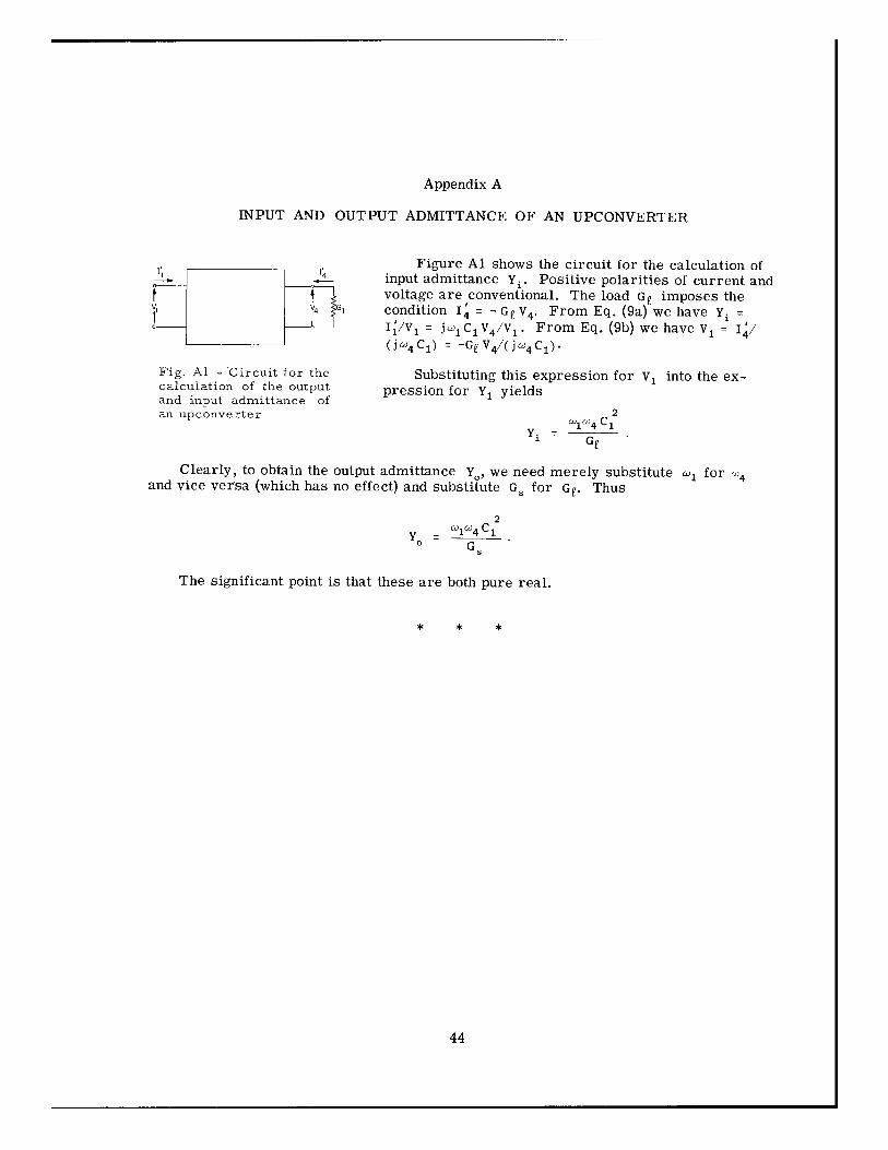
Appendix A
INPUT AND OUTPUT ADMITTANCE OF AN UPCONVERTER
Figure Al shows the circuit for the calculation ofinput admittance Yi. Positive polarities of current andvoltage are conventional. The load Gf imposes theV1 Gi condition I -= - Ge V4 . From Eq. (9a) we have Y. =I,/V1 = Wj1 C 1 V4 / V1 . From Eq. (9b) we have V1 = 1/(joj 4 C1 ) = -GFV 4/(j- 4 C 1)"
Fig. Al - Circuit for the Substituting this expression for V1 into the ex-calculation of the output pression for Y1 yieldsand input admittance ofan upconverter 1 2
Yi - Ge •
Clearly, to obtain the output admittance Y., we need merely substitute co1 for W4and vice versa (which has no effect) and substitute G. for Ge. Thus
2Yo =-lwc
Gs
The significant point is that these are both pure real.
* * *
44