
Panagiotis Tsakonas - TU Delft
147
Design and development of a 72 kV cable Y- joint with integrated PD sensor for offshore wind turbine grid connections Panagiotis Tsakonas Technische Universiteit Delft Challenge the future
Transcript of Panagiotis Tsakonas - TU Delft

Design and development of a 72 kV cable Y-
joint with integrated PD sensor for offshore
wind turbine grid connections
Panagiotis Tsakonas
Tec
hn
isch
e U
niv
ersi
teit
Del
ft
Challenge the future


Design and development of a 72 kV cable Y-joint
with integrated PD sensor for offshore wind
turbine grid connections
By
Panagiotis Tsakonas
in partial fulfilment of the requirements for the degree of
Master of Science
in Electrical Engineering - Electrical Sustainable Energy
at the Delft University of Technology,
to be defended publicly on Wednesday November 23rd, 2016 at 10:00 AM.
Student number: 4184491
Supervisors: Dr. ir. Armando Rodrigo Mor
Dr. ir. Riccardo Bodega
Thesis committee: Prof. dr. ir. P. Bauer, TU Delft
Dr. ir. Armando Rodrigo Mor, TU Delft
Dr. ir. Milos Cvetkovic, TU Delft
Dr. ir. Riccardo Bodega Prysmian Group
Ing. Jos van Rossum Prysmian Group
*Note: This thesis has been redacted for publication, due to confidentiality agreements with Prysmian Group Netherlands
B.V.

The work in this thesis was supported by Prysmian Group Netherlands B.V. Their cooperation is
hereby gratefully acknowledged.
Copyright © Prysmian Group Netherlands B.V.
All rights reserved

Acknowledgements
This master thesis is the result of the work performed this year, in order to obtain the Master of Science degree in Electrical Engineering at Delft University of Technology. This work was made possible through the support of Prysmian Group Netherlands B.V. and the department of Electrical Sustainable Energy of TU Delft.
Firstly and foremost I am thankful for the assistance, fruitful discussions and faith of my daily supervisor from Prysmian Group, Dr. Riccardo Bodega. He offered me a wonderful opportunity to work on a challenging project and provided me with an advanced technical background. Also, I would like to express my sincere gratitude to my daily supervisor from TU Delft Dr. Armando Rodrigo Mor, for his continuous guidance and valuable academic input in this project. They both helped me steer in the right direction throughout this project work and I am therefore grateful for having them my mentors.
Secondly, I would like to express my appreciations to Ir. Jos van Rossum and Ir. Wouter Geertsma from Prysmian Group Netherlands for their significant comments and expert advice in technical areas that I was unfamiliar with before the start of this project.
Moreover, I feel thankful to TU Delft for supplying me the necessary resources (hardware and software) that had been essential for conducting successfully my study. The same applies for Prysmian Group for giving me the opportunity to conduct the study in their facilities in Delft.
I would also like to mention the warm welcome and hospitality from the personnel of the High voltage laboratory at TU Delft, during part of my work there.
I owe gratitude to all my friends in Delft and colleagues from Prysmian Group for their companionship.
Lastly, I thank the people who have been always with me through the last two years of studies, my family and
Eleftheria.


Abstract
The recent developments in the offshore wind industry are pushing towards upgrading the inter-array
voltage level from 33 kV to 66 kV. The main reason behind this, is the increased capacity of future wind
turbines leading to an increased power density in the inter-array grid of the offshore wind farms. The current
level of 33 kV cannot give cost effective solutions due to the larger conductor cross-section and the longer
inter-array cables needed to accommodate the anticipated power output of future wind turbines. The option
of increasing the voltage level seems much more realistic from technical and financial point of view, taking
also into account the years of experience and technical “know how” of the manufacturers of high voltage
equipment.
The challenge for them now is to first optimize their products for the requirements of the offshore wind
industry and secondly offer solutions that reduce the total investment cost, which is usually the fact for high
voltage energy projects. For this reason, newly developed HV cable accessories are required, that follow the
simplicity of the MV products used so far in the offshore wind industry. Such is the 72 kV Y-joint or branch
joint intended to connect the inner-turbine cable with the two inter-array cables, each arriving from an
adjacent wind turbine. This type of joint can offer significant reduction in the investment costs of future wind
farm projects by reducing the number of switching facilities and as well as minimizing installation and
maintenance costs. It is therefore very promising to develop such a product for the needs of the offshore
wind industry market.
This thesis will deal with the design of a 72 kV Y-joint and propose a development testing program. The focus
will mainly be on making a compact and robust design that can successfully withstand the electrical, thermal
and mechanical stresses that are expected throughout its lifetime. Due to the importance of the Y-joint as
electrical component in the high voltage circuit, partial discharge detection would be a very desirable feature
for the end customer. For this reason a feasibility study is conducted for designing a “smart” version of the
product with integrated partial discharge sensor.
The method of finite element analysis (FEA) is widely used throughout this work due to the complex design
of the Y-joint. The advanced software and computational power available nowadays, allows three
dimensional models to be simulated with multiple physics coupled with each other. These simulations will
help identify highly stressed spots and allow correction actions to be made in the design of the product before
this is released for production. Furthermore, FEA enables design optimization that will make the product
more robust and more compact. The FEA simulations will assess: 1) the electrical stresses in the insulating
materials of the Y-joint, caused by the nominal voltage as well as the expected overvoltages in the system, 2)
the thermal behaviour of the Y-joint under both steady state and cycle loading conditions, that will determine
its current carrying capability and 3) the mechanical stresses in the epoxy insulator from the production
stage and mechanical stresses encountered during normal operation and short circuit conditions.
After completing this stage, the output of the analysis will be used to plan a development testing program
that can stress to the limits the Y-joint validating the models used during the design process. After a successful
completion of the development test program the product can be released and the type test can commence to
certify that the product meets the relevant standards.


i
Contents
1. Introduction ........................................................................................................................................ 1
1.1. Wind farm inter-array grid voltage from 33kV to 66kV ........................................................................ 2
1.2. High voltage cable accessories in a wind farm. ....................................................................................... 3
1.2.1. Dry type cable terminations. ............................................................................................................ 3
1.2.2. Cable joints. ........................................................................................................................................ 3
1.2.3. Three cable branch joints - Wye/Tee-joints. ................................................................................... 3
1.3. High voltage cable joints ........................................................................................................................... 5
1.3.1. Y-branch joints .................................................................................................................................. 7
1.4. Withstand requirements for high voltage cable joints ........................................................................... 8
1.5. Partial Discharge detection. ...................................................................................................................... 9
1.6. Design evaluation via finite element analysis ....................................................................................... 10
1.7. Thesis objectives ..................................................................................................................................... 12
1.8. Thesis outline ........................................................................................................................................... 13
2. Y-joint’s basic components Electrical field analysis ..................................................................... 15 2.1. Basic components-requirements and limitations ................................................................................. 15
2.1.1. Epoxy insulator. ............................................................................................................................... 15
2.1.2. Silicon rubber joint. ......................................................................................................................... 16
2.2. Electrical field withstand requirements ................................................................................................ 18
2.3. Initial sizing of the epoxy insulator. ....................................................................................................... 19
2.4. Outdoor protection and fixation scheme. .............................................................................................. 21
2.5. Commissioning test - Blind plug. ............................................................................................................ 22
2.6. Electrical field computation via FEA. ..................................................................................................... 22
2.6.1. Theoretical formulation. ................................................................................................................. 22
2.6.2. Building the 3D geometry. .............................................................................................................. 23
2.6.3. Boundaries and material properties. ............................................................................................. 24
2.6.4. Mesh generation. ............................................................................................................................. 25
2.6.5. Results. ............................................................................................................................................. 26
2.7. Design evaluation -recommendations. .................................................................................................. 29
3. Partial Discharge sensor design ...................................................................................................... 31 3.1. Origin of partial discharges .................................................................................................................... 31
3.2. Measuring partial discharges ................................................................................................................. 32
3.2.1. General requirements of a PD measuring system. ........................................................................ 33

ii
3.2.2. Capacitive coupler. .......................................................................................................................... 34
3.2.3. Effect of RLC circuit values on coupler’s performance. ................................................................ 36
3.2.4. Limitations. ...................................................................................................................................... 38
3.3. Designing the capacitive coupler’s electrode ........................................................................................ 39
3.3.1. Electrode type I - M8 metallic insert. ............................................................................................. 39
3.3.2. Electrode type II - Disc plate. ......................................................................................................... 41
3.3.3. Electrode type III - Coaxial cylindrical insert. ............................................................................... 43
3.4. Evaluation of electrode designs ............................................................................................................. 46
3.5. Capacitive coupler response in time domain. ....................................................................................... 47
3.6. Conclusions .............................................................................................................................................. 52
4. Thermal Analysis .............................................................................................................................. 53 4.1. Heat sources in a HV system .............................................................................................................. 54
4.1.1. Conductor losses ............................................................................................................................. 54
4.1.2. Dielectric losses ............................................................................................................................... 55
4.1.3. Sheath and armour losses .............................................................................................................. 55
4.2. Heat transfer ............................................................................................................................................ 56
4.2.1. Heat transfer mechanisms. ................................................................................................................. 56
4.2.2. Energy balance equations. .............................................................................................................. 58
4.2.3. Steady state and transient rating. .................................................................................................. 59
4.3. Literature recommendations on the thermal design of a joint ........................................................... 59
4.4. FEM thermal analysis of an XLPE cable in air. ...................................................................................... 60
4.4.1. Finite Element Analysis model. ...................................................................................................... 60
4.4.2. Calculation of cable’s ampacity. ..................................................................................................... 63
4.4.3. Calculation of thermal time constant. ............................................................................................ 64
4.4.4. Heat cycle testing. ........................................................................................................................... 64
4.5. Thermal characteristics of 60 kV XLPE cables in air. ........................................................................... 65
4.6. Thermal analysis of Y-joint. .................................................................................................................... 66
4.6.1. FEM model. ...................................................................................................................................... 66
4.6.2. Thermal characteristics of the Y-joint. .......................................................................................... 68
4.6.3. One leg disconnected- Effect on ampacity. .................................................................................... 73
4.6.4. Type test heating cycles -Effect of thermal time constant. .......................................................... 73
4.7. Evaluation of results - Conclusions. ....................................................................................................... 76
5. Mechanical loading ........................................................................................................................... 77 5.1. Theoretical formulation.......................................................................................................................... 77
5.1.1. Von Mises yield criterion. ............................................................................................................... 79

iii
5.1.2. Thermal stress and strain. .............................................................................................................. 80
5.2. Mechanical stresses on Y-joint ............................................................................................................... 81
5.2.1. Thermomechanical forces from connected cables. ...................................................................... 81
5.2.2. Stresses due to short circuit currents. ........................................................................................... 83
5.2.3. Thermal stress during production. ................................................................................................ 87
5.3. Yield strength of fixation components ................................................................................................... 87
5.3.1. Brass threaded inserts - Adhesion with epoxy. ............................................................................. 87
5.3.2. Yield strength of M8 bolts. .............................................................................................................. 88
5.4. Withstand capability of Y-joint under uniaxial loads. .......................................................................... 88
5.4.1. Building the 3D geometry. .............................................................................................................. 90
5.4.2. Boundary conditions and domain properties. .............................................................................. 90
5.4.3. Mesh generation. ............................................................................................................................. 91
5.4.4. Results. ............................................................................................................................................. 92
5.5. Thermal stress during a short circuit. ................................................................................................. 101
5.5.1. Boundary conditions and domain properties. ............................................................................ 101
5.5.2. Mesh generation. ........................................................................................................................... 102
5.5.3. Results. ........................................................................................................................................... 102
5.6. Thermal stress during production. ...................................................................................................... 105
5.6.1. Boundary conditions and domain properties. ............................................................................ 106
5.6.2. Mesh generation. ........................................................................................................................... 107
5.6.3. Results. ........................................................................................................................................... 107
5.7. Conclusions. ........................................................................................................................................... 109
6. Development tests .......................................................................................................................... 111 6.1. Initial product inspection and measurement ...................................................................................... 111
6.2. Electrical tests ........................................................................................................................................ 112
6.3. Experimental verification of the embedded PD sensor. ..................................................................... 113
6.4. Thermomechanical tests ....................................................................................................................... 114
6.4.1. Temperature cycle test.................................................................................................................. 114
6.4.2. Current heating cycle test. ............................................................................................................ 114
7. Conclusions & future scope ........................................................................................................... 119 7.1. Concluding remarks on the simulation results ................................................................................... 119
7.2. Recommendation for future research ................................................................................................. 120
APPENDIX A1 - Calculation of capacitance via FEA ........................................................ 121
APPENDIX A2 - MATLAB scripts ............................................................................................... 122
APPENDIX B - Thermomechanical forces from cables .................................................... 125
Bibliography ............................................................................................................................................ 127

iv

v
List of figures
Figure 1. Expected size and power output increase of a single wind turbine ...................................................... 2
Figure 2. Comparison of 33 kV (left) and 66 kV(right) inter-array cable arrangement [3]. ............................... 2
Figure 3. HV accessories in a wind turbine (picture from Prysmian's brochure [4]) .......................................... 3
Figure 4. Submarine and wind turbine cable connection - single and multi- line representation. .................... 4
Figure 5. Medium voltage Tee connector for cable to cable connection prior to transformer bushing. ........... 4
Figure 6. Basic representation of a two cable joint. ............................................................................................... 6
Figure 7. Construction of a 275 kV YJ [6] ................................................................................................................ 7
Figure 2.1 Conical interface of epoxy insulator. .................................................................................................... 16
Figure 2.2 Rubber joint used for the connection between insulator and cable. ................................................ 16
Figure 2.3 Interface between epoxy and silicone rubber. .................................................................................... 17
Figure 2.4 a) Standard impulse 1.2/50 μs wave, b) Breakdown characteristic, c) Voltage life as function of
the field strength. .................................................................................................................................................... 18
Figure 2.5 Y-joint insulator concept 3D drawing. ................................................................................................. 19
Figure 2.6 Cut view of Y-joint’s conductor. ........................................................................................................... 19
Figure 2.7. M8 brass insert ..................................................................................................................................... 20
Figure 2.8 Y-joint insulator a) Cross-sectional view, b) three dimensional view. ............................................. 20
Figure 2.9 Y-joint installed assembly overview. ................................................................................................... 21
Figure 2.10 Commissioning test arrangement. ..................................................................................................... 22
Figure 2.11 a) 3D geometry of the Y-joint for electrostatics simulation, b) Cross-sectional view. .................. 24
Figure 2.12 a) High voltage surface boundary, b) Ground surface boundary. ................................................... 25
Figure 2.13 Generated tetrahedral mesh. .............................................................................................................. 25
Figure 2.14 Electrical field plot- xz symmetry plane. 1 kV applied [kV/mm]. ........................................................... 26
Figure 2.15 Electrical field plot of a) surface aluminum conductor and b) highly stressed areas [kV/mm]. .. 26
Figure 2.16 Electrical field on the M8 inserts [kV/mm] ....................................................................................... 27
Figure 2.17 Electrical field of the mostly stressed insert [kV/mm] .................................................................... 27
Figure 2.18 Silicone rubber- Electrical field [kV/mm] and equipotential lines plots. ....................................... 27
Figure 2.19 Tangential electric field at the interface Si-Epoxy. ........................................................................... 28
Figure 2.20 Blind plug electrostatic simulation: a) Contour line for plotting electrical field norm, b) electrical
field surface plot [kV/mm], c) electrical field norm along the HV electrode. ..................................................... 28
Figure 3.1 Type of internal discharges [12]. ......................................................................................................... 31
Figure 3. 2 a) Equivalent circuit for internal discharges, b) Recurrent discharge phenomenon during AC
voltage c) Discharge pattern characteristic for cavities, classic detection. ........................................................ 32
Figure 3.3 Typical arrangement of a wideband PD measuring system. .............................................................. 33
Figure 3.4 a) typical harmonic and continuous interference spectrum on-site , b) frequency spectra of PD
current pulses, c) Bandpass charecteristic of PD measurement systems. .......................................................... 34
Figure 3.5 Equivalent circuit of capacitive coupler. ............................................................................................. 34
Figure 3.6 Bode diagrams of capacitive coupler showing the effect of a) capacitance ratio, b) inductor and c)
resistance. ................................................................................................................................................................ 37
Figure 3.7 Bode plot with varying stray capacitances C2. .................................................................................... 38

vi
Figure 3.8 Single layer round coil. ......................................................................................................................... 38
Figure 3.9 Conceptual drawing of the sensor’s electrode embedded in the insulator’s body. ......................... 39
Figure 3.10 An M8 insert used as PD sensor’s electrode. .................................................................................... 40
Figure 3.11 Bode plot of capacitive coupler with M8 insert used as sensor's electrode. ........................................ 40
Figure 3.12 Electrical field on the surface of the sensor's electrode -1000 V applied [kV/mm]. ..................... 41
Figure 3.13 FEM model - Disk plate (D=40 mm) used as PD sensor's electrode. .............................................. 41
Figure 3.14 Bode plot of capacitive coupler with disc plate. .................................................................................... 42
Figure 3.15 Electrical field on conductor and on the surface of the disc plate (D=100 mm) -1 kV applied
[kV/mm] .................................................................................................................................................................. 42
Figure 3.16 Electrical field plot and equipotential lines plot for disc type electrode. ....................................... 43
Figure 3.17 FEM model - Coax. cylinder used as PD sensor's electrode. ............................................................ 44
Figure 3.18 Electrical field on conductor and on the surface of the coaxial sensor -1000V applied [kV/mm].
.................................................................................................................................................................................. 44
Figure 3.19 Electrical field plot and equipotential lines plot for coaxial cylinder electrode. ........................... 45
Figure 3.20 Bode plot of capacitive coupler with coaxial cylinder electrode. .................................................... 45
Figure 3.21 Bode plot of capacitive coupler with coaxial cylinder electrode - effect of parasitic capacitance.
.................................................................................................................................................................................. 46
Figure 3.22 Bode plot comparison for the three electrode types. ....................................................................... 47
Figure 3.23 Waveform of PD pulses. ..................................................................................................................... 49
Figure 3.24 Frequency spectrum of PD pulses. .................................................................................................... 49
Figure 3.25 Capacitive couplers simulation circuits at OrCAD Capture CIS a) PD pulse input and b) Power
frequency input. ...................................................................................................................................................... 49
Figure 3.26 Input and output PD signals from OrCAD Capture CIS simulation. a) Positive pulse from needle
defect, b) positive pulse from void defect and c) negative pulse from void defect. ........................................... 50
Figure 3.27 Input and output 50Hz signals obtained from OrCAD Capture CIS simulation. ............................ 51
Figure 3.28 a) Frequency spectrum of lightning impulse and b) waveform of impulse at the input and output
of the capacitive coupler. ........................................................................................................................................ 51
Figure 4.1 FEA geometry for 36kV cable in air ..................................................................................................... 61
Figure 4.2 Domain where joule losses are computed. ......................................................................................... 62
Figure 4.3 Domains where heat transfer physics apply. ...................................................................................... 62
Figure 4.4 Meshed simulation domain. ................................................................................................................. 63
Figure 4.5 a) Step response to I=955 A, b) Temperature distribution at t=24 h, [°C] ....................................... 63
Figure 4.6 Temperature measurements for actual heating cycle of the 36kV 1x1000mm2 Al cable. .............. 64
Figure 4.7 FEA of 24 hour heating cycle. ............................................................................................................... 65
Figure 4.8 The 3D model for thermal simulation of the Y-joint. ......................................................................... 67
Figure 4.9 Temperature response for step increase of the current at I=1450 A through leg 1 and 2 (scenario
I -Al cable). ............................................................................................................................................................... 68
Figure 4.10 Loading scenario I for aluminum conductor cables and I=1450 A a) Temperature distribution
inside the joint at equilibrium [°C], b) Current density plot at equilibrium (A/mm2). .................................... 69
Figure 4.11 Electrical conductivity of aluminum conductor [S/m] .................................................................... 69
Figure 4.12 Loading scenario II for aluminum conductor cables and I=1480 A a) Temperature distribution
inside the joint at equilibrium [°C], b) Current density plot at equilibrium (A/mm2). .................................... 71
Figure 4.13 Loading scenario III for aluminum conductor cables and I=1448 A a) Temperature distribution
inside the joint at equilibrium [°C], b) Current density plot at equilibrium (A/mm2). .................................... 72

vii
Figure 4.14 BaTemperature response for step increase of the current at I=1635A through leg 1 and 2
(scenario I -Cu cable). ............................................................................................................................................. 72
Figure 4.15 Temperature distribution inside the joint at equilibrium. Leg 1 without cable, Leg 2 and 3 with
aluminum conductor cables I=1350 A. .................................................................................................................. 73
Figure 4.16 Y-joint and cable temperature response during 1st heating cycle. a) 1200 mm2 Al cable and Y-
joint b) 1600 mm2 Al cable and Y-joint. ................................................................................................................. 74
Figure 4.17 Y-joint and cable temperature response during 1st heating cycle. a) 1200 mm2 Cu cable and Y-
joint b) 1600 mm2 Cu cable and Y-joint. ................................................................................................................ 74
Figure 4.18 Y-joint and cable temperature response during 5 heating cycles.1600 mm2 Al cable and Y-joint.
.................................................................................................................................................................................. 75
Figure 4.19 Y-joint and cable temperature response during 5 heating cycles. 1600 mm2 Cu cable and Y-joint.
.................................................................................................................................................................................. 75
Figure 5.1 a) Components of stress in three dimensions, b) Principal stresses. ................................................ 78
Figure 5.2 Stress-strain curve typical for steel. .................................................................................................... 79
Figure 5.3 a) Force versus temperature characteristic for a restrained single core cable with Milliken
conductor, b) Tensile and compressive forces generated in a single-core cable during loading cycles [37]. 82
Figure 5.4 Most severe short circuit current path inside YJ. ................................................................................ 83
Figure 5.5 Short circuit current waveform. ........................................................................................................... 84
Figure 5.6 Temperature versus short circuit duration for a) Isc=50 kA and b) Isc=100 kA ............................... 86
Figure 5.7 Insulator with embedded M8 threaded brass inserts. ....................................................................... 87
Figure 5.8 M8 RVS-70 hex. socket bolt. ................................................................................................................. 88
Figure 5.9 Direction notation of applied forces. ................................................................................................... 89
Figure 5.10 a) Imported 3D geometry of Y-joint insulator and b) Generated mesh with tetrahedral elements.
.................................................................................................................................................................................. 90
Figure 5.11 a) Fixed constraint boundaries, b) loading surface for compressive/tensile forces at leg 2 and c)
loading surface for cantilever forces at leg 2. ........................................................................................................ 91
Figure 5.12 Compressive load 34.5 kN, a) displacement 3D plot [mm], b) Von Mises plot [MPa].Deformation
factor 300. ................................................................................................................................................................ 93
Figure 5.13 Compressive load 34.5 kN, Von Mises stresses at aluminum conductor [MPa] a) 3D view and b)
across cut plane 1. ................................................................................................................................................... 94
Figure 5.14 Compressive load 34.5 kN, a) Von Mises stresses in epoxy across cut plane 1[MPa], b) cut plane
1. ............................................................................................................................................................................... 95
Figure 5.15 Compressive load 34.5 kN, a) Von Mises stresses in epoxy at the inserts’ surface [MPa], b) Von
Mises stress in epoxy across cut plane 2[MPa], c) Cut plane 2. ........................................................................... 95
Figure 5.16 Identification of M8 inserts. ............................................................................................................... 96
Figure 5.17 Cantilever loading 22 kN, a) displacement 3D plot [mm], b) Von Mises plot [MPa].Deformation
factor 80. .................................................................................................................................................................. 97
Figure 5.18 Cantilever loading 22 kN, Von Mises stresses at aluminum conductor [MPa] a) 3D view and b)
across cut plane 1. ................................................................................................................................................... 98
Figure 5.19 Cantilever loading 22 kN, a) Von Mises stresses in epoxy across cut plane 1[MPa], b) cut plane 1.
.................................................................................................................................................................................. 99
Figure 5.20 Cantilever loading 22 kN, a) Von Mises stresses in epoxy at the inserts’ surface [MPa], b) Von
Mises stress in epoxy across cut plane 2[MPa], c) Cut plane 2. ........................................................................... 99
Figure 5.21 Mesh for thermal stress simulation during short circuit. .............................................................. 102

viii
Figure 5.22 Thermal expansion 80°C to 195°C a) Displacement plot [mm] b) Von Mises plot [MPa]-
Deformation factor 50. ......................................................................................................................................... 103
Figure 5.23 Thermal expansion 80°C to 195°C. Von Mises stresses at aluminum conductor [MPa] a) 3D view
and b) across cut plane 1. ..................................................................................................................................... 103
Figure 5.24 Thermal expansion 80°C to 195°C. Von Mises stresses at epoxy [MPa] a) 3D view and b) across
cut plane 1. ............................................................................................................................................................. 104
Figure 5.25 Thermal expansion 80°C to 195°C. Von Mises stresses at epoxy close to inserts [MPa] a) 3D view
and b) across cut plane 2. ..................................................................................................................................... 104
Figure 5.26 Allowable short circuit level as function of the duration, θc=195°C and θin=80°C. ..................... 105
Figure 5.27 a) meshed geometry, b) fixed point constraint, c) Roller surface condition, d) Symmetry plane and e)
Fixed temperature boundary. ................................................................................................................................ 107
Figure 5.28 Thermal shrinkage 80°C to 20°C a) Displacement plot [mm] b) Von Mises plot [MPa]-
Deformation factor 20. ......................................................................................................................................... 108
Figure 5.29 Thermal shrinkage 80°C to 20°C a) Von Mises plot of aluminum conductor [MPa] b) Traction
stress at interface with epoxy [MPa]. ................................................................................................................ 108
Figure 5.30 Thermal shrinkage 80°C to 20°C von Mises plot in epoxy [MPa]. ................................................. 109
Figure 5.31 Thermal shrinkage 80°C to 20°C von Mises plot in epoxy around inserts. .................................. 109
Figure 5.32 Short circuit withstand curve. ......................................................................................................... 110
Figure 6.1 Critical dimensions of Y-joint insulator. ............................................................................................ 111
Figure 6.2 Electrical tests arrangement. ............................................................................................................. 113
Figure 6.3 Test loop for validation of Y-joint's PD sensor [1]. ........................................................................... 114
Figure 6.4 Heating cycle test loop. ....................................................................................................................... 115

ix
List of tables
Table 2.1: Maximum permissible field strengths, U0= 36 kV. .............................................................................. 18
Table 2.2: Relative permittivity of insulating materials. ...................................................................................... 25
Table 2.3: Electrical field values- Summarizing table .......................................................................................... 29
Table 3.1: Capacitive coupler performance - electrode type I ............................................................................ 40
Table 3.2: Capacitive coupler performance - electrode type II ........................................................................... 42
Table 3.3: Capacitive coupler performance - electrode type III ......................................................................... 46
Table 3.4: Design evaluation table. ........................................................................................................................ 47
Table 3.5: Characteristics of typical defect PD pulses. ............................................................................................ 48
Table 4.1: Cable specifications: 20.8/36 kV 1x1000mm2 Al / 25mm2 Cu ......................................................... 60
Table 4.2: Material properties applied at each geometry domain. ..................................................................... 62
Table 4.3: Thermal characteristics of 60 kV XLPE cables, Tamb=25°C ............................................................... 65
Table 4.4: Material properties for domains in Y-joint model ............................................................................. 66
Table 4.5: Thermal characteristics of Y-joint at Tamb=25°C ................................................................................. 70
Table 5.1: Tensile Yield strength of YJ insulator's materials. .............................................................................. 80
Table 5.2. Mechanical and thermomechanical properties of YJ materials. ......................................................... 81
Table 5.3: Tensile/Compressive forces in Nt from cables with copper conductor and aluminum sheath..... 83
Table 5.4: Direction of forces per loading scenario. ............................................................................................. 89
Table 5.5: Material properties for mechanical simulation. .................................................................................. 90
Table 5.6: Epoxy/brass interfacial stress per insert ............................................................................................ 93
Table 5.7: Epoxy/brass interfacial stress per insert- cantilever load. ............................................................... 97
Table 5.8: Design limits per loading scenario. ................................................................................................... 100
Table 5.9 Material properties for thermal expansion simulation. .................................................................... 102
Table 5.10: Epoxy/brass interfacial stress per insert- thermal stress. ............................................................. 104
Table 5.11: Material properties for thermal expansion simulation. ................................................................. 106
Table 5.12 Tensile/Compressive forces in Nt from cables with aluminum conductor and aluminum sheath.
................................................................................................................................................................................ 125
Table 5.13 Tensile/Compressive forces in Nt from cables with aluminum conductor and lead sheath. ...... 125
Table 5.14 Tensile/Compressive forces in Nt from cables with copper conductor and lead sheath. ........... 125

x

1 1. Introduction
The ever increasing energy demand and the race to meet by 2020 the EU goal of 20% production of the total
consumed energy by renewables, has led north European governments to develop plans for massive,
renewable source-based, power production. According to the NEO (Netherlands Energy Outlook) report [1],
the renewables share at the Dutch energy scheme is expected to be in the range of 10.5% and 13% by 2020.
This is below the Dutch target (14% in 2020) that has been agreed in the European context, and therefore a
long and challenging road lies ahead in order to meet the next target of 16% in 2023.
The offshore wind energy will be the backbone of the renewable sources and can help the Netherlands
achieve this ultimate target. Mostly it’s due to the excellent conditions for offshore wind energy production:
relatively shallow waters, good wind resource, good harbour facilities, experienced industry and a robust
support system [2]. Nevertheless, the current technology and practises for commissioning new windfarms
proves to be insufficient for the timeframe which is given.
According to the National Energy Agreement the target for the offshore wind capacity is to increase from
todays 1,000 MW to 4,500 MW in 2023. The Dutch government has designated three new wind farm zones
and has introduced a new approach for the deployment of the new wind farms, allowing more efficient use
of space, cost reduction and acceleration of the deployment of offshore wind energy [2].
In order to increase the offshore wind capacity by 3,5 GW in less than 10 years, all involved parties such as
Ministries, energy organizations and industries need to come together and come up with innovative ideas.
Among others the High Voltage cable industry has been summoned to this cause. Since, its usual market could
be considered rather conservative, an opportunity window has been opened for developing new high voltage
products aimed specifically for the offshore wind industry.
This thesis deals with the design and development of one of these new products: the 72 kV three cable branch
joint or Y-joint. It is going to be one of the most vital components for the future wind farm’s inter-array grid,
offering significant reduction in investment as well as maintenance costs. Due to its first appearance in the
high voltage portfolio, the branch joint has to be carefully designed, thoroughly tested and certified according
to the most demanding standards.
Its non-axis-symmetric design and its complex function in the HV circuit, compared to that of a common two
cable joint, makes it more difficult to define its electrical limits, its ampacity, its mechanical strength and its
short circuit withstand characteristic. In addition, the demand for a compact and simple design, set challenges
in maximizing the electrical, thermal and mechanical performance. Furthermore, the integration of an
effective partial discharge sensor without compromising the performance of the Y-joint, needs special
approach and deep understanding of the detection techniques proposed in literature. All the aforementioned
challenges are tackled in a scientific and engineering way, as described in more detail hereafter in this thesis
report.
2 Introduction
1.1. Wind farm inter-array grid voltage from 33kV to 66kV
Nowadays the maxim capacity of offshore wind farms stays in a range below 600 MW, while the common voltage level for the inter-array grid is limited to the 33 kV. In order to increase the Dutch offshore wind capacity by 3,500 MW, the Dutch government agreed to develop three new wind-park zones in the North Sea, meaning that each zone will be able to supply up to 1.2 GW of electrical power to the system [3].
Furthermore, considering that the single capacity of future wind turbines is going to increase to 8 MW and more, the 33 kV voltage level cannot give a cost effective solution in transferring such amount of power. It is thus, expected that a higher voltage level of 66 kV will be used. By transferring to a higher voltage, the amount of power delivered by the same conductor cross sectional area, increases. Of course extra costs arise by increasing the insulation thickness to accommodate for the proper clearances needed for this higher voltage level. But these are not comparable to the cost of increasing the cross section of a copper or aluminium conductor. To be more precise, based on information from well-known cable manufacturer’s the prices of 66kV cables would be 10% and 20% higher than the 33 kV cables of the same conductor cross-section, which is outweighed by the doubling of the transfer capacity [3].
Figure 1. Expected size and power output increase of a single wind turbine
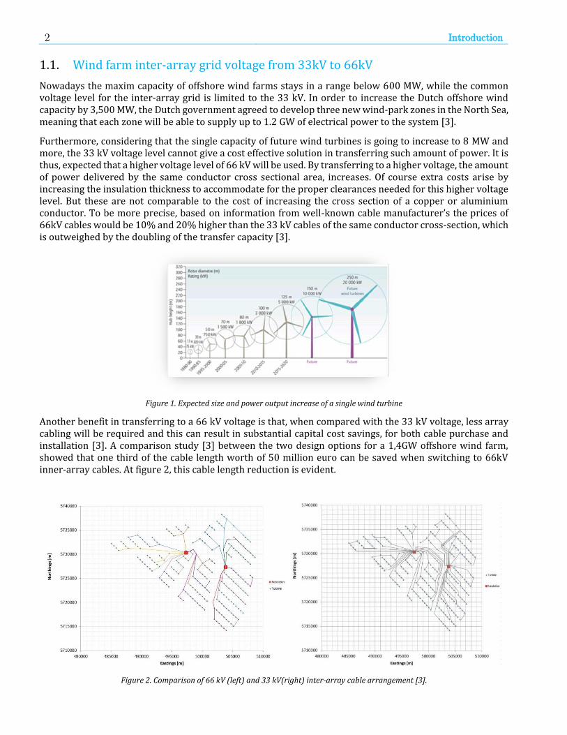
Another benefit in transferring to a 66 kV voltage is that, when compared with the 33 kV voltage, less array cabling will be required and this can result in substantial capital cost savings, for both cable purchase and installation [3]. A comparison study [3] between the two design options for a 1,4GW offshore wind farm, showed that one third of the cable length worth of 50 million euro can be saved when switching to 66kV inner-array cables. At figure 2, this cable length reduction is evident.
Figure 2. Comparison of 66 kV (left) and 33 kV(right) inter-array cable arrangement [3].

3 Introduction
1.2. High voltage cable accessories in a wind farm.
Since the increase of the inter-array voltage from 33 kV to 66 kV necessitates a step from medium voltage to high voltage, a whole new market opens for the High Voltage industry. Manufacturers of high voltage equipment such as cables, cable joints, terminations, switchgears, transformers etc. are able to offer their equipment to multimillion worth of projects. Especially for producers of HV cables, the profits from such projects are quite significant, as approximately 300 km of submarine HV cables could be installed in a wind farm with designed capacity of 1,400 MW [3].
Also for the manufacturers of HV cable accessories, this market opportunity cannot be ignored since the amount of accessories to be installed per wind farm is quite big.
1.2.1. Dry type cable terminations.
Inside a wind turbine one step-up transformer (point 1-figure3) and at least one switchgear box will be needed. Both will require dry-type cable terminations for connection with the HV cables. In case the switchgear box is placed at the HV side, in total nine dry type cable terminations per wind turbine have to be installed.
Of course, all the 66 kV inter-array cables of the wind farm, end up at an offshore substation. From figure 2, we can see that approximately 10 lines arrive at the substation, meaning that 10x3=30 dry type cable terminations will be necessary to connect the inter-array cables to the substation.
Considering a wind farm with total capacity of 1,400 MW, at least two substations and 175 wind turbines (8 MW each) must be installed. This amounts to a total of 1605 dry type cable terminations.
1.2.2. Cable joints.
Depending on the location of the transformer and switchgear inside a wind turbine, HV cables might be necessary to transfer the power from the generator located at the nacelle. These will be preinstalled onshore inside the tower segments before been transferred to the wind farm site. Depending on the wind turbine’s height (>100 m) the tower could be divided into more than 3 column segments. This means two connection points for the HV cable inside the tower (point 2-figure 3), translated into 6 cable joints.
For a 1,400 MW windfarm with at least 175 wind turbines( 8 MW each) the number of supplied cable joints amounts to 525.
1.2.3. Three cable branch joints - Wye/Tee-joints.
Figure 3. HV accessories in a wind turbine (picture from Prysmian's brochure [4])
1
2
3

4 Introduction
As can be seen from figure 2, wind turbines are grouped into array circuits (feeders), which all end up at one of the offshore substations. The number of wind turbines connected to each circuit depends on the nominal power of each wind turbine, the transfer capacity of the submarine cables and the topological layout of the wind farm itself. As an example, for an array circuit with a 66 kV 630 mm2 copper conductor cable, around 80MW could be transmitted [3]. This means that up to 10 wind turbines, 8MW each, could be connected in one circuit. If 5 MW wind turbines are to be used, then up to 16 wind turbines can be connected to one single circuit.
All wind turbines of one circuit are connected in parallel and each connection takes place inside the tower of the wind turbine (figure 4). The two submarine cables (three core cables) coming from the adjacent wind turbines enter the tower. A splitter is used to separate the three cores and align them to the connection interface. The HV cables coming from the nacelle of the wind turbine are also aligned to be connected. From figure 4 it is clear that per phase, a three cable connection must be made, called “Y-joint” or “T-joint” connection.
Usually such connection takes place inside the 66 kV switchgear which forms the interface between the wind turbine electrical system and the subsea array cable network. According to DNV-GL report [3], although this is a standard product offering within the electrical power industry, it is not a tailor made solution for wind turbine technology. Well known switchgear manufacturers supply standard switchgear available for rated voltages of 72.5 kV. However the dimensions of such switchgear types and configurations tend to be excessive and not generally lend themselves to installation inside the turbine tower. Air insulated switchgear (AIS) solutions for 72.5 kV are similarly excessive for such installations. SF6 insulated switchgear (GIS) is significantly smaller but more costly than air insulated versions. Furthermore, SF6 might be banned in the near future, requiring other solutions such as vacuum technologies. Nevertheless, some key manufacturers are going through the process of establishing designs specifically targeted at
Figure 4. Submarine and wind turbine cable connection - single and multi- line representation.
Figure 5. Medium voltage Tee connector for cable to cable connection prior to transformer bushing.

5 Introduction
the offshore wind market. Some of such solutions are already commercially available while others are very close to commercial availability.
However, in existing windfarms, operating at middle voltage level, the triple joint connection may as well take place outside a switchgear compartment. Typical MV connection solutions are offered by manufacturer’s that give the ability for connecting two or even three cables to electrical equipment (transformers, switchgear and motors). This approach, leads to less and cheaper switchgear boxes, thus a lot of capital savings which is essential for offshore wind projects. Furthermore, due to its simplicity, the installation is easy and fast, which is quite essential for offshore installations in which the man-hour cost is very high.
To sum up, the use of high voltage switchgear to accommodate the “Y-joint” connection may be a risky and expensive solution. The added cost for switchgear installation increases with the number of wind turbines and the SF6 might be forbidden to be used as insulating medium in the near future. A different approach must be followed, that will introduce the simplicity of the MV sector to the 66 kV high voltage level.
The 72 kV cable branch joint or ‘Y-joint”(point 2-figure 3) is a new HV product, designed according to this concept. For each wye-connection(figure 4) inside a wind turbine, 3 Y-joints will be needed. The total cost of this solution is expected to be 3 and 4 times less than the price of a 3-phase switchgear including its control schemes. Thus, the total capital spent for a wind farm project could be reduced by several million euros. Furthermore, the joint can be easily installed and will require no maintenance for the rest of its lifetime.
Main drawback of this solution is the inability to isolate faults. For instance, a fault close to the last wind turbine of a feeder would trigger the circuit breaker located at the other end of the feeder, thus shutting down all the generators downstream. If instead, a switchgear is placed in each wind turbine the circuit breakers located in it would isolate the fault and the rest wind turbines would remain connected to this line. Of course, if such faults are extremely unlikely to happen, the extra capital spend for switchgears and relays is not justified. Risk analysis studies need to be made and most probably hybrid solutions containing both switchgear and Y-joints will be adopted.
For the time being, the “Y-joint” as part of Prysmian’s complete offshore 66 kV cabling solution, has been approved by Tennet (the Dutch TSO and offshore grid operator appointed by the Dutch government). Furthermore, according DNV-GL expectations, there will be no obstructive certification issues with respect to the main electrical systems within the wind turbine.
Therefore, having the TSO approval and considering the large quantities of HV cable accessories, it is easy to conclude that the prospect of developing new cable accessories, specifically for the needs of the wind offshore industry, seems now very reasonable and worth any investment cost for R&D purposes. The rest of this thesis report will deal with the design, simulation and testing program for the development of the 72 kV Y-joint.
1.3. High voltage cable joints
Cable joints, together with terminations are classified as cable accessories and form an essential part of a cable system. Joints are necessary for jointing different lengths of cables in order to reach the required circuit length [5]. According to the International Electrotechnical Vocabulary, a joint is defined as: “Accessory making a connection between two cables to form a continuous circuit”. This is because, the cable lengths to be jointed are limited by the manufacturing facilities, the transport/shipping equipment or the installation conditions [5]. The joint construction includes:
A mechanical and electrical connection between the cable conductors.
Proper insulation and shielding around the conductor connection.
Direct electrical connection of the cable sheaths/screens or special bonding connection for losses reduction.

6 Introduction
A covering that protects the joint from the environment and houses the continuity of the connection scheme of the cable sheaths/screens.
Joints can be placed underground, buried or installed in manholes or tunnels. They have larger diameter than that of the cable and are of rigid type [5]. Joints exist also for submarine cables and have approximately the same diameter as the cable and can be bend under tension.
Nowadays, HV and EHV joints are mostly intended for extruded insulation cables which have replaced oil-filled paper cables due to environmental reasons. They can be classified into families according to their function, and to sub-families depending on their design, manufacturing and installation technologies. The main families are [5]:
Straight through joints: Joints that connect two cables of the same insulation type. If the construction of the two cables differs in terms of conductor or diameters the straight joints is called asymmetric.
Transition joints: Joints that connect two cables of different insulation type.
Screen interruption joints: Joints incorporating a semi-conductive and metallic screen interruption for cross-bonding connections.
Y-branch joints: Joints that connect three cables.
Joints can be prefabricated or manufactured on site with non-pretested components. The prefabricated joints include rubber (EPR or Silicone) components (and sometimes epoxy components) moulded in the factory, under controlled conditions. All prefabricated joints are routine tested before sent to the field to ensure high reliability [5].
Of special interest are the “plug-in” type straight through joints. The factory prepared cable ends are slipped through the bore of the rubber joint and via spring loaded pins they lock to a metal ring incorporated in the joint. Its main advantage is the fast assembly of the joint in the field and the factory controlled preparation of the cable ends. Prysmian Cables and Systems utilizes this technique at the “Click-Fit” family of accessories.
A good contact pressure is necessary, between the rubber of the joint and XLPE insulation of the cable, as from an electrical point of view, the interface between the two materials is the most critical part of the joint. This pressure is ensured by stretching the rubber sleeve as the prepared cable slides through the bore. The diameter of the cable insulation is larger than that of the bore and a conical shape at the beginning of the cable end takes care the smooth transition between the two. Depending on the size of the joint, special tools such as hydraulic piston tool or chain-hoist tool must be used to slide the rubber sleeve on the cable core.
1.Cable conductor 2.Cable insulation 3.Joint insulation 4.Conductors connection (mechanical and electrical) 5.
Cables’ screen connection 6. Semiconductive HV electrode 7. Semiconductive ground electrode 8.External
protection
Figure 6. Basic representation of a two cable joint.
4 3 1 2 5 6 7 8

7 Introduction
1.3.1. Y-branch joints
As mentioned in section 1.2.3, there are situations where three cables need to be connected. For instance when a new HV substation is built in an urban region, generally an existing underground transmission line must be diverted and drawn into the new substation [6]. When applying instead a Y-branch Joint (called hereafter YJ), significant cost reduction of switching facilities and cabling can be achieved. These joints are not so common in Europe but they have been used widely in Japan for the 66 kV class and have been qualified for up to the 275 kV voltage class. A typical construction of a 275 kV YJ (XLPE-XLPE/Fluid filled) is shown at the following picture.
Figure 7. Construction of a 275 kV YJ [6]
The basic components of the YJ are:
1. Prefabricated (casted) epoxy insulator: This is the centrepiece of the joint, housing the metallic insert where the cables’ conductors are connected mechanically and electrically. It also takes care of the proper electrical field distribution inside its volume (shielding electrodes etc.).
2. Metallic insert: Usually made out of aluminium with silver plated contact surfaces for optimum current flow between the insert and conductor ferule. The insert also ensures the proper mechanical connection with them. Furthermore it is carefully designed in places where it has to serve as shielding electrode.
3. Conductor ferule: Serves as transition interface between the cable conductor and the insert. It must withstand the same current as the cable conductor without overheating and must support the thermos-mechanical forces transferred by the cable during thermal cycles [5]. Most common types are compression connectors, mechanical bolted connector and plug-in connectors. The latter will be the case for the developed YJ.
4. Prefabricated rubber part: Has a function same as in the typical joint, which is to ensure a contact pressure at the interface surfaces with the epoxy and the cable’s insulation (XLPE).
5. Protective casing for the insulator.
6. Protective casing for the rubber and XLPE cable.
Similarly to the typical joints, the YJ could have additional functions. It can be connecting cables of different insulation material, thus acting as a transition joint, or it could connect cables of different conductor diameter, thus acting as an asymmetric joint. It could also incorporate interruption of the semi-conductive and metallic screen for cross-bonding connections. Furthermore, the YJ can be buried or placed in manholes in both horizontal and vertical position.
2 4 1 2 3 5

8 Introduction
When only two cables are connected with the YJ, for instance during commissioning tests of part of the circuit, then the third unconnected end can be closed via a properly designed plug, called the “blind-plug”. In this case the YJ is actually behaving as a normal two cable joint.
1.4. Withstand requirements for high voltage cable joints
During their life time, cable joints are subjected to various types of stresses, which they must withstand without any risk of failure. The origins of these stresses are briefly explained below:
Electrical stresses: Are expressed in (kV/mm) which is the electrical field the insulating material can withstand without breakdown. It originates from the system’s operating voltage and overvoltages. The voltage Uo refers to the nominal r.m.s. voltage between the HV part (conductor or
semiconductive screens) and ground. The phase to ground voltage may reach a value of Um/√3 , where Um (the maximum voltage for equipment) is the maximum phase to phase voltage applied continuously to the system. Apart from the continuously applied system’s voltage, the system may experience additional transient or dynamic overvoltages. These are correlated with Um and Uo by standards (e.g. IEC 600071-1), and depending on the waveform and duration these overvoltages are grouped into the Basic Impulse Level (BIL), Switching Impulse Level (SIL) and short duration AC industrial frequency withstand level. The joint must be able to withstand all those voltage stresses without a breakdown.
Thermal stress due to load current: Ohmic losses are generated due to the current flowing through the conducting parts of the cable and the joint. These losses generate heat which is dissipated to the environment. Due to its increased dimensions, a joint has different thermal properties compared to the connected cable, and if the load current becomes high for a prolonged period of time, the heat generated inside the joint may give rise to temperatures that hinder the electrical and mechanical performance of the joint. According to reference [7] the joint must be able to withstand conductor temperatures comparable or higher than the rated temperatures of the cable.
Mechanical stress due to load current: The variation with time of the conductor current generates thermo-mechanical stresses inside the joint due to the different thermal expansion coefficients of its components. Furthermore, current variation generates longitudinal thrust/traction forces of the cable conductor to the locking device of the joint. These forces depend on the cable construction, on its fixation method (rigid or flexible) before and after the joint and on the installation conditions.
Other mechanical stresses: Flexural forces may occur from short circuit currents or misalignment of the cable and joint’s axis. These are much less in magnitude compared to the axial forces mentioned above but still generate compression and tension stresses at the joint’s components. Furthermore, elastomeric bodies in EPR or silicon rubber compounds, are stretched on the cable core or on other components of the joint (e.g. epoxy insulator), to provide a sufficient pressure at the interface [5].
Environmental stresses: the accessories maybe placed at various environments, thus they may be subject to rain, moisture condensation, salt fog, air pollution, UV radiation etc. For this reason, a joint’s insulation must be enclosed in a protective shell (metallic or non-metallic), which also protects the operators against risk of contact with energised parts in case an accidental damage of the joint occurs.
The Y-joint will be subject to all these stresses and must be able to withstand those throughout its lifetime which is more than 40 years. For this reason all parts of the YJ must be tested electrically, thermally and mechanically. Initially, a battery of development tests should be performed, after production of the first prototypes, to validate the design’s expectations and to energise possible faults that were not predicted during the designing phase. After successful development testing, the fully assembled YJ must be type tested to identify its long term performance. In type testing the YJ is tested as complete system, and that is with the cables it connect. Depending on the voltage class and the type of cables connected, it must meet specific
9 Introduction
international and national standards. For HV accessories, the International Standard IEC-60840-“Power cables with extruded insulation and their accessories for rated voltages 30kV(Um = 36 kV) up to 150 kV (Um = 170kV) -Test methods and requirements” [10] is in effect.
Thermal and mechanical ratings
It should be noted that specific requirements regarding the thermal and mechanical behaviour of cable joints are not explicitly mentioned in the standard. Regarding their thermal rating, they were generally considered to have equal or better levels than those of the cable. A Task Force( TF 21(B1)-10) launched by IEC Technical Committee 20, had addressed questions raised, of whether and how thermal and thermomechanical ratings of accessories( joints and terminations) should be defined [7]. The basic conclusion of this task force was that “thermal ratings for accessories need not be specified separately from cables, as they are considered identical due to the presence of cable inside the accessory. The successful completion of the IEC thermal tests at the complete cable system can be considered as simultaneous verification of the adequate thermal design of both, cables and accessories, provided that comparable or higher conductor temperatures as rated for the cable are achieved inside joints. These test conditions shall be achieved by current heating only”.
Nevertheless, thermal limit’s and mechanical forces on joints have to be considered by the system’s design engineering, and thus the following information should be available from the manufacturer [7]:
1. The basic thermal characteristics of the accessory (i.e. thermal time constants of the joint, thermal resistance between conductor and outer covering of the joint).
2. The value of admissible mechanical forces acting on the joint.
1.5. Partial Discharge detection.
One of the most important phenomena to be monitored in a high voltage system, is the partial discharge activity. This is because partial discharges have been recognised as a harmful aging process for electrical insulation, and their fast detection can save transmission and distribution systems from devastating failures.
Partial discharges (PDs), are generated by defects such as voids, contaminants or protrusions, located inside the polymeric insulation of HV cables and joints. They generate both physical and chemical changes, deteriorating the dielectric material and reducing the lifetime of the insulation. HV cables are produced under controlled conditions in a factory, and are always routine tested just after production, thus eliminating defects before the installation phase. Joints on the other hand, are assembled onsite, meaning that their proper functioning depends on the installation conditions and the skills of the jointing personnel. Especially for prefabricated joints, due to the presence of interfaces of different insulating materials, defects can develop and the induced PDs will deteriorate the interfacial insulation and initiate electrical treeing. It is thus no surprise that most of the defects that generate PDs are more likely to exist within cable joints than in the cable itself [8].
For this reason it is important to develop online PD measurement techniques and post processing tools that can detect PDs and serve as diagnostic tool for cable joints. General guidelines for measuring and evaluating PDs are given by the International Standard IEC 60270, which mainly focuses on electrical detection methods. Non-electrical methods such as optical, acoustical and chemical detection also exist, but are more suitable locating the PDs rather than for quantitative assessment. For on-line PD monitoring via non-convectional electrical coupling, the following approaches are mainly followed [8]:
By means of capacitive coupler: a coaxial cable sensor is installed forming a voltage divider via the capacitance between the sensor’s electrode and the conductor’s section. Usually it is necessary to remove part of the metallic earth screen to form the sensor’s electrode. Then a measuring impedance is connected between the electrode and the screen so discharge pulses can be measured. For safety reasons, overvoltage protection is installed in parallel with the measuring impedance to avoid

10 Introduction
harmful voltages reaching the measuring equipment in case of faults. To isolate PDs internal to the joints from external pulses, coupling sensors can be placed on either side of the joint [8]. Main advantage of using capacitive couplers is their high detection sensitivity.
By means of inductive couplers: coils are clamped around the cable to detect the magnetic fields caused by the PD current pulses. These are more suitable for cables with screens consisting of individual cables in a helical arrangement, in which the axial magnetic field component can be detected, using only a coreless single turn open loop inductive coupler.
By means of radio frequency current transducers: toroidal current transformers are placed around the conductor connecting the metallic screen of the cable with the ground. These capture the magnetic field (radial component) generated by the discharge current pulse flowing through it. The generated signal is proportional to the rate of change of the magnetic flux through the loop. The easy installation and minimal modification of the cable/joint system is the method’s main advantage.
Common drawback for the aforementioned methods is their susceptibility to electrical noise and interference. Thus the main challenge of an online PD detection system is to isolate the PD signals form background noise levels with sufficient quality and ascertain the presence and type of PD activity.
PD detection in a Y-joint
For the developed Y-joint, a partial discharge detection system would be of great importance due to the number and variety of interfacial surfaces. In a normal two cable prefabricated joint the interfaces are located at the two sides of the joints and pertain to two insulating materials, that of the joint (silicone rubber) and that of the cable (XLPE or EPR). In a Y-joint though, the interfaces are located at six connection points (3 times cable-rubber and 3 times rubber-insulator) and pertain to three insulating materials: silicone rubber, XLPE/EPR and epoxy. Furthermore, since it is the connection of three cables, the Y-joint is a junction point for external PDs propagating through the cable system, thus it would the most favourable point to place a PD monitoring device.
In this thesis, the possibility of equipping the Y-joint with an integrated capacitive coupler for PD measurements is investigated. Various geometries for the coupler’s electrode will be simulated using finite element software. The sensor should be a viable solution in terms of manufacturability, cost and interoperability. It should also not increase the risk of failure of the Y-joint and must not pose any danger to personnel.
1.6. Design evaluation via finite element analysis
Nowadays finite element analysis (FEA) is widely used by engineers as a development tool, suitable for finding and solving potential or existing performance issues in components and structures. It is a simulation tool and is based on the finite element method (FEM): a numerical technique for finding approximate solutions in boundary value problems. The boundary value problems are defined by a region, governed by partial differential equations (PDE) describing single or multiphysics problems, and a set of constraints called the boundary conditions. In the FEM, the domain of the problem is divided into small entities called elements and the PDEs are transformed into energy related functionals. After defining the initial values of the problem, approximate solutions are sought to the field problem that minimize (or extremize) these functionals [10]. More precisely, the steps involved in the FEM modeling are as follows [11]:
1. Build a geometry model of the device to be simulated. Some FEM commercial packages contain the appropriate interfaces to build it. In case of complex geometries it is better to use computer aided design (CAD) software to make the model. Depending on the device under consideration it is useful to identify symmetries before making the model. In this way an axis symmetric device for example can be simulated using a 2D model instead of 3D model, thus saving considerable computational time.

11 Introduction
2. Define the physics applied on the model. The governing physical processes are described by partial differential equations which form the basis for the laws of science. These must be accompanied by initial and boundary conditions. This step can be considered as the most important part of the analysis, as non proper definition (or understanding) of the physics and boundary conditions applied, will result in misleading results.
3. Define the domain properties. This step concerns the assigning of material properties to all domains. An accurate simulation relies on good material data. These can be provided by the manufacturer on found online. They can be constant or a function of other parameters such as temperature, electric field, frequency etc.
4. Mesh generation. The geometry is divided into small entities called elements. Different types of mesh generation and mesh refinement exist. For 2D models with complex curvatures the triangular elements are mostly used. For 3D models four types of mesh element are used - tetrahedral, bricks, prisms and pyramids, with tetrahedral being the most common.
5. Solving the problem. The governing partial differential equations are discretized in space (and time) and the resulting linear(or non-linear) systems of equations are solved to minimize an energy-related functional. The system converges to a solution.
6. Post processing the results: The potential solution of the PDEs are visualized on the mesh employed for discretization in space and time. Other quantities can be derived by the obtained solution and then visualized as well.
These are the basic steps in the FEA process. Depending on the FEM software, the hardware (memory, processing power, etc.) and the user’s skills, a simulation model can give quite results. The computational time is usually a limiting factor and mainly increases with the complexity of the geometry, the mesh density and the number of simulated physical processes. A good model should give a good approximate solution in a reasonable amount of time. This means that simplifications of the model and sometimes of the physics cannot be avoided, and the user must be able to do that without significantly reducing the accuracy of the model output.
FEA on the Y-joint
As mentioned already, FEA is a valuable tool for designing and developing new products. It is actually a virtual test room that can help engineers evaluate the design prior to manufacturing and testing of the component. Potential flaws of the design can be readily identified thus decreasing the total risk, and the design can be optimized thus reducing significantly the manufacturing costs. For all these reasons, the final design of the Y-joint must be supported by finite element analysis simulations. Due to the complexity of the Y-joint, the model’s geometry will be built three-dimensional using a common CAD software. The finished geometry will then be imported in COMSOL Multiphysics software to perform the finite element analysis. Throughout this thesis the following studies will be performed:
Electrostatic study. For sizing of the Y-joint’s epoxy insulator and determining the electrical field distribution inside the insulation (Chapter 2). It will be also used for the design of the PD sensor and specifically for determining the capacitance values of different electrode arrangements (Chapter 3).
Current heating study. This will assess the thermal behaviour of the Y-joint as heat is produced due to the current flowing through the conductor. Critical parameters such as the ampacity and the thermal time constant can be calculated via time dependent studies. Dynamic conditions such as heat cycle loading will be also investigated through this type of study. (chapter 4)
Thermo-mechanical study. The time dependent study will be used to investigate the thermo-mechanical stresses induced by the different thermal expansion coefficients of aluminium and epoxy. Thermomechanical stresses develop both during production and during normal operation (heat cycle and short circuit).Chapter 5)

12 Introduction
Structural mechanics study. For determining the maximum axial and cantilever forces that can be applied on the Y-joint structure. (Chapter 5)
For both thermal and thermomechanical studies we take advantage of the multiphysics coupling feature that COMSOL offers.
1.7. Thesis objectives
Based on the recent developments on the offshore wind industry, concerning the upgrade from 33 kV to 66 kV of the inter-array grid, Prysmian Cables and Systems B.V. is enriching its portfolio of 72.5 kV accessories with the addition of the CFYJ-72 Y-joint. As part of a complete solution (cable and accessories) the CFYJ-72 will offer significant reduction in the total windfarm cost and is thus already positively welcomed by the offshore market. The Click-Fit® accessories department at Delft has accepted the challenge to design, produce and qualify this new product.
Aim of this thesis is to design a robust and smart 72.5 kV Y-joint able to meet all requirements set by the relevant standards. Furthermore, it must be cost effective and comparable to the MV accessories in terms of simplicity in design and installation effort. The main objectives are listed as follows:
Initial design of the main components of the Y-joint and determining the working principle (earth continuation, electrical shielding, mechanical fixation etc.).
Sizing of the epoxy insulator and evaluation of the electrical field distribution using FEA. Identification of the critical areas in terms of electrical stressing.
Design of an integrated high frequency PD sensor for online partial discharge measurements.
Analysis of the thermal characteristics of the complete joint in static and dynamic conditions via FEA. Determination of the joint’s ampacity and thermal characteristics.
Investigating through FEA the thermomechanical stresses developed during production as well as during short circuit.
Determination via FEA of the maximum axial and cantilever mechanical forces that the Y-joint can withstand. Calculation of the actual forces expected from the thermal loading of cables and from short circuit currents.
Preparing the development testing plan for the first prototypes. The basic components of the Y-joint will be electrically and thermally tested to prove the design expectations. Test values as well as the test setup arrangements are defined.
Main challenges
The epoxy insulator must be compact enough to reduce production cost, minimize the “volume effect” and improve its thermal behaviour under prolonged high loading currents. On the other hand the electrical field increases when the dimensions of this component decrease, thus allowing small room for manufacturing errors that could lead to dielectric breakdown. A fine balance should be found between those two counteracting factors.
The electrical field withstand capability of the joint depends on both the stress in the bulk of its insulating materials and interfacial stress between two insulating materials. Furthermore the withstand value depends also on the type of applied voltage (i.e. waveform shape, peak value and duration). The electrical withstand capability must thus be examined in space as well as in time domain.
Before designing the partial discharge sensor, the effect of the main RLC circuit values on the sensors response must be examined. The capacitance of the electrode towards the HV part and towards the ground

13 Introduction
must be obtained using data of the FEM analysis. The PD sensor must be designed in a way that gives the best filter characteristics without compromising the electrical behaviour of the Y-joint.
The thermal behaviour of the joint must be assessed in both steady state and in time depended loading scenarios. The study must also take into account the multiple current paths in a Y-joint, the effect of the connected cables on the thermal capacity of the system and the effect of magnetic related phenomena such as the proximity and skin effect.
The short circuit withstand capability of the Y-joint shall be studied under both the electromagnetic forces acting on the component and the stresses caused by thermal expansion of the conductor. The critical conductor’s temperature after a short circuit shall be linked to the short-circuit current via a formula, thus giving the withstand characteristic of the Y-joint. The most critical short circuit current path must be identified first.
1.8. Thesis outline
In general, each of the following chapters in this report, contains a theoretical and simulation part. The basic
theoretical background and literature review will be presented at the beginning of each chapter. Afterwards
the appropriate FEM models are built and the simulation scenarios explained. At last the simulation results
are presented and discussed. When applicable the results are compared with the theoretical calculations.
More analytically the report is structured as follows:
Chapter 2. Electrical analysis - This chapter will focus on the electrical performance of the Y-joint. At the beginning, the mathematical formulation of the problem is established. Then the electrical field in bulk is approximated using standard concentric geometries. These values are compared to the maximum allowed values so that the main dimensions can be defined. Then the 3D model is built and imported for electrostatic simulation in the FEA software. The results are compared with the calculated values and critical spots of field enhancement are identified.
Chapter 3. Design of PD sensor - This chapter is dedicated on the design of the partial discharge sensor. I starts with a brief theoretical introduction namely on the PD origin and characteristics, and the detection via capacitive couplers. The optimum RLC values for the detection circuit are calculated. Afterwards, a number of possible electrode designs are considered for the capacitive coupler sensor. Using FEM analysis, the capacitances of electrode to HV conductor and electrode to ground, are computed. Finally, the most favourable sensor design is chosen taking also into account field stresses and produce-ability.
Chapter 4. Thermal analysis - The thermal behaviour of the Y-joint under various current loading conditions, is examined via FEM analysis. This chapter starts with an introduction in the main heat transfer mechanisms and the electromagnetic heating phenomena. The difficulties in defining the thermal rating of the joint (and of accessories in general) are pointed out, and the CIGRE recommendations are adopted for this purpose. Firstly, the results of a 2D FEM simulation for a HV cable are cross-checked with actual measurements performed in the lab. A second 2D simulation will be made to determine the rated current of the cable connected at the Y-joint (for max cable conductor temp. 90°C). This will serve as the heating current input for the Y-joint simulation model. With this input current the temperature distribution inside the Y-joint assembly will be evaluated. It should be noted that, in this analysis, the Y-joint should be treated as a two cable joint. This means that each loading scenario will be applied three times, corresponding to the three paths the max current can follow.
Chapter 5. Mechanical analysis - In this chapter the Y-joint will be evaluated in terms of mechanical stressing. At first, an introduction is made into the basic theory behind the types of mechanical stresses and the Von Mises criterion. Afterwards, an analysis is made of all types of expected mechanical and

14 Introduction
thermomechanical stresses on the Y-joint. A 3D model is build and simulated for all possible loading schemes. The thermal stresses will checked via in time dependent simulaton.
Chapter 6. Development tests - Following the evaluation of the design, a list of tests is proposed for the electrical, thermal and mechanical assessment of the first prototypes. A test for determining the effectiveness of the integrated PD sensor is also proposed.
Chapter 7. Conclusions -Conclusions are drawn and suggestions for further research are made.

2
2. Y-joint’s basic components Electrical field analysis
This chapter will deal with the design of the basic electrical components of the Y-joint: the epoxy insulator and the silicon rubber parts. The transition from the cable to the rubber joint and from the rubber joint to the epoxy insulator must be fully controlled from an electrical field point of view, meaning that the electrical stress must remain below the breakdown limits of the insulating materials. Furthermore, since there are three kind of insulating materials, there are two kind of interfaces and the tangential stress on those interfaces must also stay below the maximum allowable stress levels.
The components must be designed to be as small as possible. This is very important, especially for the offshore wind industry, since compactness translates into low transport and installation costs. Furthermore, the thermal behavior of the components improves, since the thermal resistance is increasing with the volume of the insulation. The production cost also decreases and a small volume of insulation reduces the risk per product regarding manufacturing errors.
Therefore, a fine balance must be achieved between compactness and the maximum electrical fields developed inside the Y-joint. With the aid of finite element analysis, the electrical field inside the Y-joint can be accurately computed and the dimensions can be optimized to achieve the best solution.
2.1. Basic components-requirements and limitations
The main purpose of the Y-joint is to joint three cables in a correct manner. As briefly mentioned in chapter 1 the electrical continuation is realized by two basic components 1) the silicone rubber joint and 2) the epoxy insulator. The so far technical know-how of Prysmian’s Click-fit dry type cable terminations will be utilized in this product.
2.1.1. Epoxy insulator.
The epoxy insulator is the centrepiece of the Y-joint. First of all, it is the component at which the electrical node of the circuit is realized. Depending on the circuit arrangement, one leg will always carry more current than the other two, unless the current at one of the legs is zero. This shall be taken into account when deciding the conductor diameter.
Similarly to a cable, the insulator must have a means of screening the high voltage conductor. For this component a zinc coating is applied at the outer surface of the epoxy, which will be normally grounded and connected with the semiconductive outer layer of the rubber joints.

16 Y-joint’s basic components - Electrical field analysis
Furthermore, the epoxy insulator houses the three interfaces for connection with the rubber joints of the YJ. The interface will be of outer cone type, similar to the dry type cable terminations of the Click-Fit family. This conical interface has well established dimensions, regarding the slope φ and the conductor connector which must follow the click-fit concept (figure 2.1). The height of the cone depends on the length l of the interface which must be long enough for the interfacial strength to not exceed the limit values. In adittion it must be long enough to allow for the rubber to slide freely without being blocked by the base of the cone.
The zinc coating around the epoxy insulator must end at a specific height at the base of each cone, to properly countinue the grounded screen to the semiconductive layer of the rubber. This means that the edge on the base will serve as a guiding electrode and thus must be rounded with a an adequate radius.
From a mechanical perspective the Y-joint needs to be mounted on the metallic frame inside the wind turbine. For this reason the insulator shall have metallic inserts integrated in its body that will firmly fix it on a mounting plate.
2.1.2. Silicon rubber joint.
The rubber joint performs the mechanical and electrical connection between the cable and the insulator. The cable end is prepared by properly removing the sheath and semiconductive layer for a specified length. The cable conductor is stripped from the insulation and a click-fit connector is pressed or welded on it. Inside the rubber, a brass insert is used to secure the Click-fit ends of the cable and the insulator respectively. The brass insert will also house a copper bushing ring, for properly conducting the electrical currents from the cable conductor to the epoxy conductor. The electrical contact surfaces of the click fit ends are silver coated to minimize contact resistance.
Figure 2.2 Rubber joint used for the connection between insulator and cable.
In order to avoid field enhancement at the HV side, all metallic parts at the connection zone are screened via
a semiconductive electrode. Furthermore, the semiconductive stress cones at both sides control the electrical
field at the transition between the grounded screen of the rubber joint and the screens of the cable and epoxy.
When the joint is inserted in the insulator’s cone the rubber is stretched and pressure is applied on the
interface between the two materials. This pressure increases the tangential electrical strength of the
interface. In the same manner, contact pressure is applied by the rubber on the cable insulation when the
cable is inserted in the bore of the joint.
Figure 2.1 Conical interface of epoxy insulator.
Click-Fit
connector
Zinc
coating
Epoxy
Silver
coating
Epoxy coneClick-Fit connectors
Brass insertCopper ring
HV stress control
electrodeStress cone cable side
Stress cone epoxy sideCable semicon layer

17 Y-joint’s basic components - Electrical field analysis
The main dimensions of the rubber joined are already defined since it is part of the 72 kV dry type cable
termination of the click-fit family. The bore diameter and the dimensions of the brass insert depend on the
construction of the cable and are also already defined. Nevertheless, the stress cone at the epoxy side needs
to be redesigned in order accommodate a secure transition between the zinc coating of the insulator.
2.1.2.1. Stress cone epoxy side - Interface epoxy-Si.
Interfaces between two dielectric materials are one of the weak spots in cable joints. The equipotential lines
cross the interface at a varying angle resulting in a tangential electrical field. This electrical field stresses the
interface which has lower dielectric strength than the insulating materials. By changing the profile of the
stress cone at the epoxy side this tangential field at the Si-epoxy interface is affected. Therefore, the tangential
field must be checked against reference values when redesigning this profile.
In addition the end of the zinc coating at the base of the epoxy cone, must be overlapped by the stresscone. If
not, this will become a point of field enhancement and breakdown will occur. The principle is illustrated at
figure 2.3.
In general, the following parameters were taken into consideration before designing the stress cone:
a. The maximum electric field inside the Si-rubber must remain below reference value.
b. The maximum tangential electric field at epoxy-Si interface must remain below reference value.
c. The triple point junction must be shielded (low e-field).
d. The length of the electrode’s surface in contact with the epoxy should be long enough to ensure proper shielding of the ending line of the metal coating.
e. A ±4mm deviation in total joint’s length due to manufacturing errors.
f. A -4mm change in total joint’s length due to shrinking under cold conditions.
g. Compression due to change in cone’s angle.
Stress cone
End of metal coating
Figure 2.3 Interface between epoxy and silicone rubber.
Triple point junction
Conductor

18 Y-joint’s basic components - Electrical field analysis
2.2. Electrical field withstand requirements
All insulating materials in a high voltage system are subject to electrical stresses during normal operation. As
briefly mentioned in chapter 1, these stresses originate from the system’s operating voltage as well as from
overvoltages. The overvoltages can be either power frequency waveforms of increased amplitude and short
duration, or impulses of specific rise and fall time.
These voltages are replicated in type tests and prequalification tests, and are therefore standardized in shape
and value. For the voltage class of Um=72.5 kV the basic voltage impulse level (BIL) is at 325 kV. According
to the standard IEC-60840, the insulating materials of the tested accessory, must be able to withstand 10
positive and 10 negative voltage impulses with a 1.2/50 μs waveform (figure 2.4a) with peak value of 325
kV. For the same voltage class, the rated short duration power frequency withstand voltage is at 140 kV for
1min, according to the standard IEC-60071.
The breakdown characteristic of an insulating material depends a lot on the shape of the applied overvoltage.
As can be seen at figure 2.4b, the withstand value increases for steep and short impulses. Furthermore, for
power frequency overvoltages the voltage life characteristic is essential, as the total time to breakdown
decreases when average electrical field increases (figure 2.4c). This is the reason why at type tests, the test
objects are subjected to overvoltages of short duration. An accessory passing this test can guarantee to the
utility that no breakdown of the insulating material will occur throughout the designated operational lifetime.
Figure 2.4 a) Standard impulse 1.2/50 μs wave, b) Breakdown characteristic, c) Voltage life as function of the field strength.
Table 2.1: Maximum permissible field strengths, U0= 36 kV.
Epoxy [kV/mm]
Silicone rubber [kV/mm]
Si-Epoxy tan. E-field
[kV/mm]
1 minute overvoltage @ 140 kVrms : 13.3 17.4 3.2
Lightning impulse @ 325 kV : 28.5 37.2 7.7
Minimum normalized value @ 1 kV : 0.0877 0.1145 0.0228
a) b) c)
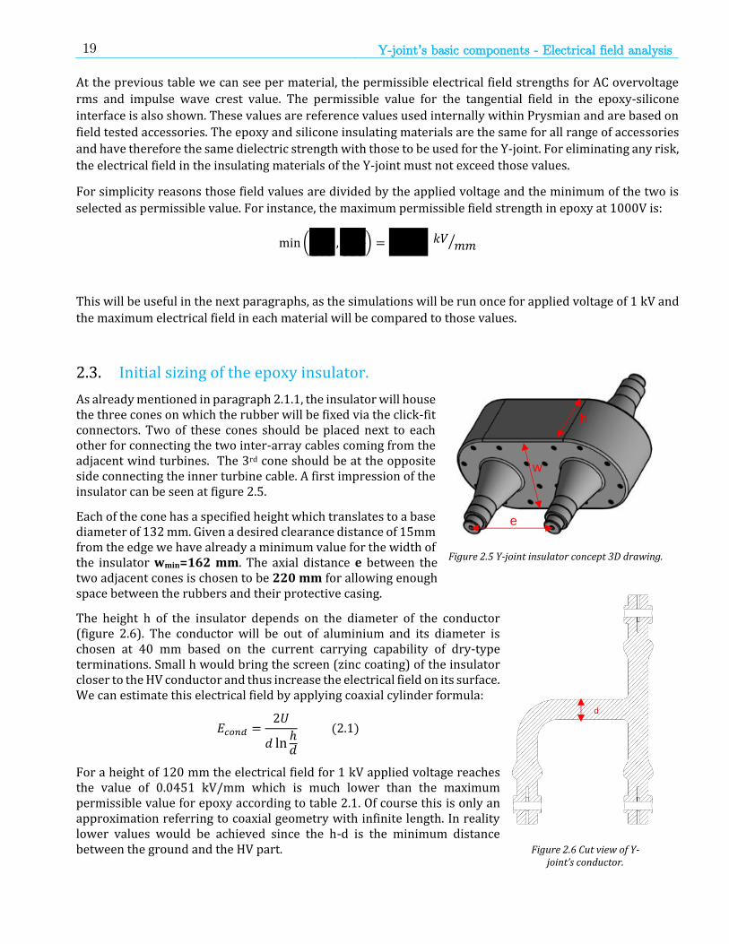
19 Y-joint’s basic components - Electrical field analysis
At the previous table we can see per material, the permissible electrical field strengths for AC overvoltage
rms and impulse wave crest value. The permissible value for the tangential field in the epoxy-silicone
interface is also shown. These values are reference values used internally within Prysmian and are based on
field tested accessories. The epoxy and silicone insulating materials are the same for all range of accessories
and have therefore the same dielectric strength with those to be used for the Y-joint. For eliminating any risk,
the electrical field in the insulating materials of the Y-joint must not exceed those values.
For simplicity reasons those field values are divided by the applied voltage and the minimum of the two is
selected as permissible value. For instance, the maximum permissible field strength in epoxy at 1000V is:
min (13.3
140,28.5
325) = 0.0877 𝑘𝑉 𝑚𝑚⁄
This will be useful in the next paragraphs, as the simulations will be run once for applied voltage of 1 kV and
the maximum electrical field in each material will be compared to those values.
2.3. Initial sizing of the epoxy insulator.
As already mentioned in paragraph 2.1.1, the insulator will house the three cones on which the rubber will be fixed via the click-fit connectors. Two of these cones should be placed next to each other for connecting the two inter-array cables coming from the adjacent wind turbines. The 3rd cone should be at the opposite side connecting the inner turbine cable. A first impression of the insulator can be seen at figure 2.5.
Each of the cone has a specified height which translates to a base diameter of 132 mm. Given a desired clearance distance of 15mm from the edge we have already a minimum value for the width of the insulator wmin=162 mm. The axial distance e between the two adjacent cones is chosen to be 220 mm for allowing enough space between the rubbers and their protective casing.
The height h of the insulator depends on the diameter of the conductor (figure 2.6). The conductor will be out of aluminium and its diameter is chosen at 40 mm based on the current carrying capability of dry-type terminations. Small h would bring the screen (zinc coating) of the insulator closer to the HV conductor and thus increase the electrical field on its surface. We can estimate this electrical field by applying coaxial cylinder formula:
𝐸𝑐𝑜𝑛𝑑 =2𝑈
𝑑 lnℎ𝑑
(2.1)
For a height of 120 mm the electrical field for 1 kV applied voltage reaches the value of 0.0451 kV/mm which is much lower than the maximum permissible value for epoxy according to table 2.1. Of course this is only an approximation referring to coaxial geometry with infinite length. In reality lower values would be achieved since the h-d is the minimum distance between the ground and the HV part.
h
w
d Figure 2.5 Y-joint insulator concept 3D drawing.
d
Figure 2.6 Cut view of Y-joint’s conductor.
e

20 Y-joint’s basic components - Electrical field analysis
This implies that the height h can reduce to less than 120 mm, but limitations are set by the embedded metallic inserts which are used for fixation purposes. These act as protrusions in the screen resulting in field enhancement at their tip. A way to estimate this electrical field is first to calculate the average electrical field between the conductor and the screen and then multiply it with the field enhancement factor β for cylindrical protrusion [11]:
𝛽 =2𝐻
𝐷 (2.2)
where H is the height of the insert and D is its width.
From figure 2.7 H=26 mm and D=12 mm, resulting in β=4.333. The average electrical field for d=40 mm, h=120 mm and U=1 kV is :
𝐸𝑎𝑣 =2
ℎ − 𝑑∙ ∫
2𝑈
𝑥 lnℎ𝑑
ℎ2
𝑑2
𝑑𝑥 = 0.025 𝑘𝑉/𝑚𝑚
Consequently the electrical field at the tip of the insert is:
𝐸𝑡𝑖𝑝 = 𝛽 ∙ 𝐸𝑎𝑣 = 0.10825 𝑘𝑉/𝑚𝑚
This value is above the permissible value of 0.0877 kV/mm, but refers to and insert placed in a homogeneous field of Eav and directly above the conductor. In reality the inserts will be in a non-homogenous field and will be placed at a larger distance from the conductor.
The complex three dimensional geometry as seen at figure 2.8, makes it relatively difficult to approximate the electrical field at the critical spots. Finite element analysis would be the ideal method for extracting such values from even more complex geometries. The limitations of this method are found only at the computational power and the freedom given from the relative software.
Limitations during casting process
Since the insulator will be a casted epoxy product, minimum two mold parts are necessary. After the insulator is removed from the mold, the line at which the two parts come apart leave a thin film of epoxy which must
Figure 2.7. M8 brass insert
Figure 2.8 Y-joint insulator a) Cross-sectional view, b) three dimensional view.

21 Y-joint’s basic components - Electrical field analysis
be removed via machining. This is not allowed to happen at the conical parts of the insulator, since it is the interface with the rubber joint and special roughness requirements must be met. Therefore, the only solution is to have the separation line at the xy-plane at the middle of the insulator. The inlet and outlet pipes for pouring the epoxy during casting must be placed also along this line. For avoiding air bubbles being trapped a slight slope is introduced. The
The edges are given a fillet radius of R4. The proposed design of the insulator is shown at figure 2.8. This will be the base for the making the 3-geometry to be imported at the FEA software for electrical field analysis.
2.4. Outdoor protection and fixation scheme.
The reliability of the inter-array grid relies on the uninterrupted service of both the insulator and the rubber joint. Therefore, all factors that may hinder their proper functioning during operational life time, must be eliminated. One of these factors refers to the environmental conditions expected at the installation site. For the offshore wind industry guidelines and standards exist for the protection of the electrical equipment. According to DNV·GL standard [16], “cables and their accessories installed inside the tower or nacelle outside of enclosures shall be resistant to operating fluids such as oil and grease. In case of cables and their accessories installed and laid outdoors or installed within lattice towers, UV resistance and resistance to salty moist air shall be ensured.”
For this reason the insulator and all three rubber joints are protected with UV resistant plastic covers combined with copper bell as shown at figure 2.9. The base of the covers will be fitted with sealing tape to prevent moisture penetration. At the end where the copper bell and cable meet the sealing will be provided by means of a heat shrinkable tube.
The whole protection scheme, as well as the insulator, are bolted on a mounting plate. This plate is made of aluminium with oxidized surface and will fix the whole assembly vertically on the mounting structure of the wind turbine. In case ground isolation from the mounting structure is desired support insulators can be used.
* The design and engineering of the aforementioned components are not covered in this report.
Support insulator
Figure 2.9 Y-joint installed assembly overview.
Protection
covers
Copper bell
Epoxy insulator
Rubber joint

22 Y-joint’s basic components - Electrical field analysis
2.5. Commissioning test - Blind plug.
During commissioning of the inter-array grid, a battery of electrical tests are
performed to ensure the proper installation of the submarine cables and the
proper jointing of those via the Y-joint. Initially, these tests are intended for
the inter-array grid only and not the inner turbine cabling and accessories.
For this reason, the tope cone is not connected to a cable and must thus be
terminated in a different way. The proposed solution, is to use a rubber body
(blind plug) of same conical interface with the rubber joint, but shorter and
without metallic insert (figure 2.10). The reduced volume and the absence
of the metallic part makes it a cost-effective solution.
Keeping the plug in the right place is essential, and since no metallic insert
is present, this will happen via a pushing plate that will be bolted on the
protective cover.
2.6. Electrical field computation via FEA.
In this paragraph the Y-joint (insulator, rubber joint and cable) is simulated using the electrostatics module of COMSOL Multiphysics in a stationary study. Initially the 3D geometry is built with the aid of a commercial CAD software due to the design’s complexity. Then, the model is imported in the FEM software. The physics are defined, the boundary conditions are set and the mesh is created. After completing those steps the model is processed by the software. The obtained data is post-processed to derive the wanted values and plot the electrical field at the critical points.
2.6.1. Theoretical formulation.
When working with time varying electromagnetic fields one of the fundamental laws is described by the Maxwell-Faraday equation:
∇ × �⃗⃗� = −𝜕�⃗⃗�
𝜕𝑡 (2.3)
This states that the time varying magnetic field will induce a spatially varying electric field. In high voltage engineering it is quite common to deal with electrostatic fields. In this case the time derivative at equation 2.2 becomes zero:
∇ × �⃗⃗� = 0 (2.4)
This equation indicates a conservative field at which the potential Ux at one point x is independent of route to x [11].
Figure 2.10 Commissioning test arrangement.

23 Y-joint’s basic components - Electrical field analysis
The electrical field E is a vector quantity and can be derived from the potential U, which is a scalar quantity:
�⃗⃗� = −∇𝑈 (2.5)
This equation means that the vector E points to the maximum decrease of the potential U.
The next fundamental law is the Gauss’ law:
∇�⃗⃗� = 𝜌 (2.6)
where ρ is the electric charge density and D is the electric displacement or the electric flux density and is given by the constitutive relation:
�⃗⃗� = 휀0�⃗� + �⃗� (2.7)
where ε0 is the permittivity of vacuum with value of 8.854 10-12 F/m, and �⃗� is the electric polarization vector
that describes how the material is polarized when an electric field is present. �⃗� is thus a function of �⃗� and for linear materials �⃗� = 휀0𝜒𝑒�⃗� . Equation 2.7 can be rewritten as:
�⃗⃗� = 휀0(1 + 𝜒𝑒)�⃗� = 휀0휀𝑟�⃗� (2.8)
By combining equations 2.5, 2.6 and 2.7 Gauss law can be rewritten as a variant Poisson’s equation:
−∇(휀0∇𝑉 − �⃗⃗� ) = 𝜌 (2.9)
This latter equation is used in finite element analysis to describe the electrostatics physics inside dielectric materials.
Boundary and interface conditions
To get a full description of an electrostatics problem, boundary conditions must be specified at material interfaces and physical boundaries. At an interface between two materials, the boundary conditions are expressed mathematically:
�̂�2 × (�⃗� 1 − �⃗� 2) = 0 (2.10)
�̂�2 ∙ (�⃗⃗� 1 − �⃗⃗� 2) = 𝜌𝑠 (2.11)
Where ρs is the surface charge density and n2 is the normal vector from medium 2.
Interface between dielectric and perfect conductor
At such interface the boundary conditions expressed by equations 2.10 and 2.11, are simplified. If medium 1 corresponds to perfect conductor then D1=0 and E1=0 and the equations become:
−�̂�2 × �⃗� 2 = 0 (2.12)
−�̂�2 ∙ �⃗⃗� 2 = 𝜌𝑠 (2.13)
2.6.2. Building the 3D geometry.
For the electrostatics simulation, a 3D model of all electrical components must be created, including the HV cables. The specifications of a 1200 mm2 XLPE cable are used to make the 3D model of each of the three cables. In order to reduce the complexity of the model and avoid unnecessary increase of the mesh elements, which would increase the computational time, the following simplifications are made:
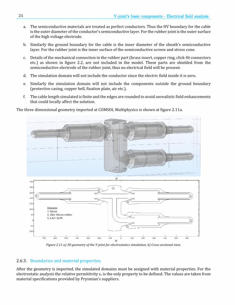
24 Y-joint’s basic components - Electrical field analysis
a. The semiconductive materials are treated as perfect conductors. Thus the HV boundary for the cable is the outer diameter of the conductor’s semiconductive layer. For the rubber joint is the outer surface of the high voltage electrode.
b. Similarly the ground boundary for the cable is the inner diameter of the sheath’s semiconductive layer. For the rubber joint is the inner surface of the semiconductive screen and stress cone.
c. Details of the mechanical connection in the rubber part (brass insert, copper ring, click-fit connectors etc.) as shown in figure 2.2, are not included in the model. These parts are shielded from the semiconductive electrode of the rubber joint, thus no electrical field will be present.
d. The simulation domain will not include the conductor since the electric field inside it is zero.
e. Similarly the simulation domain will not include the components outside the ground boundary (protective casing, copper bell, fixation plate, air etc.).
f. The cable length simulated is finite and the edges are rounded to avoid unrealistic field enhancements that could locally affect the solution.
The three dimensional geometry imported at COMSOL Multiphysics is shown at figure 2.11a.
Figure 2.11 a) 3D geometry of the Y-joint for electrostatics simulation, b) Cross-sectional view.
2.6.3. Boundaries and material properties.
After the geometry is imported, the simulated domains must be assigned with material properties. For the electrostatic analysis the relative permittivity εr is the only property to be defined. The values are taken from material specifications provided by Prysmian’s suppliers.
Domains
1: Epoxy
2, 3&4: Silicon rubber
5, 6 &7: XLPE
2
1
3
4
5 6
7
a)
b)

25 Y-joint’s basic components - Electrical field analysis
Table 2.2: Relative permittivity of insulating materials.
Epoxy Silicone rubber XLPE
Relative permitivity εr 4.5 3.1 2.3
The high voltage boundary surfaces can be seen at figure 2.12a. As already mentioned a 1 kV voltage is applied on this boundary. The outer surfaces are defined as ground boundaries (figure 2.12b).
Figure 2.12 a) High voltage surface boundary, b) Ground surface boundary.
2.6.4. Mesh generation.
All simulation domains are meshed with free tetrahedral elements. In general, a fine mesh is desired in order to obtain accurate results and good resolution at the areas of interest. This particularly important at the vicinity of the M8 inserts which are expected to develop high electrical fields. The mesh is optimized and the restrictions given are:
Minimum element size: 0.1 mm Maximum element size: 114 mm Maximum element growth rate: 1.45 Curvature factor: 0.5 Number of elements: 1.919.022
The mesh quality is assesed by the minimum element quality, which should be greater than 0.1. The generated mesh has a minimum element quality of 0.62, which is more than required.
Figure 2.13 Generated tetrahedral mesh.
a)b)

26 Y-joint’s basic components - Electrical field analysis
2.6.5. Results.
All results refer to 1kV applied voltage. The electrical field values are compared with the maximum permissible values at table 2.1. In figure 2.14 we see the electrical field plot in the symmetry xz-plane. In general the electrical field in epoxy is lower than that at the rubber and the cable insulation. We will now examine each of the critical areas that were previously identified.
Figure 2.14 Electrical field plot- xz symmetry plane. 1 kV applied [kV/mm].
Electrical field at insulator’s conductor
The maximum electrical field on the surface of the insulator’s conductor is located at the cones area (location F1 figure 2.15b) and has a value of 0.0563 kV/mm which is 64% the maximum allowable value (0.0877 kV/mm). This high field region is caused by the rubber’s stress-cone which is in close distance from the HV conductor. The horizontal leg of the conductor has a maximum field of 0.043 kV/mm and is less than that calculated using the coaxial cylinder equation 2.1.
Electrical field at M8 inserts
In the previous paragraph we expected a field enhancement at the surface of the fixation inserts, due to the close proximity to the HV conductor. As can be seen from figure 2.16, the inserts located at the centre of the epoxy insulator develop the highest electrical field, pointing towards the high voltage conductor.
Figure 2.15 Electrical field plot of a) surface aluminum conductor and b) highly stressed areas [kV/mm].
F1
F4
F3

27 Y-joint’s basic components - Electrical field analysis
Figure 2.16 Electrical field on the M8 inserts [kV/mm]
Nevertheless, this field enhancement bring it to a value of 0.046 kV/mm which is lower than the maximum value found at the surface of the conductor. It is also much lower than the approximated value of paragraph 2.3.
It should be noted though, that the quality of the inserts must be monitored before casting the insulator. Since the electrical field is comparable to that on the surface of the conductor the slightest protrusion would cause field enhancement exceeding the permissible value. Of course the same implies for the surface of the aluminium conductor.
Electrical field at silicone rubber
The highest electrical field at the silicone rubber is 0.089 kV/mm and is found at location F2 as shown in figure 2.18. This is lower than the maximum permissible value of 0.1145 kV/mm. Nevertheless the modified part is the stress cone at the epoxy side. The electrical field at this side remains at much lower values than the encountered at location F2. More specifically the electrical field at the triple point junction (F3) is 0.061 kV/mm and the field at the surface of the HV semicon (F4) is 0.064 kV/mm. This proves that the new stress-cone profile does not give any additional risk to the insulating material.
Figure 2.18 Silicone rubber- Electrical field [kV/mm] and equipotential lines plots.
Figure 2.17 Electrical field of the mostly stressed insert
[kV/mm]
F2

28 Y-joint’s basic components - Electrical field analysis
Figure 2.19 Tangential electric field at the interface Si-Epoxy.
Tangential electrical field - Epoxy-Rubber interface
As already mentioned, the interfaces between two insulating materials are considered a weak spot in high voltage systems. Therefore, the tangential electrical field along the interface of epoxy with silicone rubber, is an equally important parameter to check. Figure 2.19 shows that the highest tan-Efield is close to the stress-cone, with a value of 0.021 kV/mm. This value is lower than the maximum permissible field (0.022 kV/mm) from table 2.1, proving that the design of the stress cone is acceptable.
Electrical field calculation - blind plug
This component is designed for properly terminating the unconnected cone (or cones) of the Y-joint. The conical interface of the plug is the same as at the rubber joint. The top part though has a modified HV electrode and field calculations are necessary to optimize the profile and the distance d from the earthed screen. Figure 2.20 shows the results for a 2D axis symmetric electrostatic analysis. The electrical field at the top corner of the electrode reaches a value of 0.062 kV/mm which is not higher than in the rest insulating material and much lower than the permissible value.
Figure 2.20 Blind plug electrostatic simulation: a) Contour line for plotting electrical field norm, b) electrical field surface plot [kV/mm], c) electrical field norm along the HV electrode.
d

29 Y-joint’s basic components - Electrical field analysis
2.7. Design evaluation -recommendations.
With the aid of finite elements calculation software, the Y-joint was analysed in terms of electrical field. The weak spots that had been identified at the preliminary analysis are not critical and the electrical field remains below the permissible values given by the manufacturer.
More specifically, the maximum electrical field in epoxy is located at the conical parts of the insulator and is 63% of the permissible field, posing no risk for the component. The electrical field at the horizontal part of the conductor and on the M8 inserts is almost half of the permissible value. This means that the insulator could be more compact in the z axis and the height h could be reduced by a few mm. Nevertheless, the uncertainty in the quality of the M8 inserts makes it preferable to keep this dimension at 120 mm.
The rubber’s stress cone (at the epoxy side) was redesigned with a profile that allows the electrode to overlap with the end of the insulators zinc coating. The new profile has an effect on 1) the electrical field in epoxy, 2) the electrical field in Si and 3) the tangential field at the Si-epoxy interface. The results of the simulation show that the insulating materials and interfaces are stressed below the permissible values. Consequently, the design of the stress cone is acceptable.
The overall conclusion is that a compact and robust design of the Y-joint has been made. The electrical components (i.e. insulator and rubber parts) can be electrically tested without any risk according to the standardized voltage values for short duration AC 50 Hz and lightning impulse.
Table 2.3: Electrical field values- Summarizing table
Electrical field @ 1 kV
[kV/mm]
Permissible value@ 1 kV
[kV/mm]
% of the permissible
value
Electrical field @ 140 kV 1 min.
Electrical field @ 325 kV BIL
[kV/mm] %
permissible [kV/mm] %
permissible
Epoxy
Conductor’s surface F1
0.056 0.0877 64% 7.84 57% 18.2 64%
M8 insert surface
0.046 0.0877 52% 6.44 48% 14.9 52%
Si
F2 0.089 0.1145 78% 12.5 72% 28.9 78%
F3 0.061 0.1145 53% 8.54 49% 19.8 53%
F4 0.064 0.1145 56% 8.96 52% 20.8 56%
Epoxy-Si interface 0.021 0.0228 92% 2.94 92% 6.83 89%

30 Y-joint’s basic components - Electrical field analysis
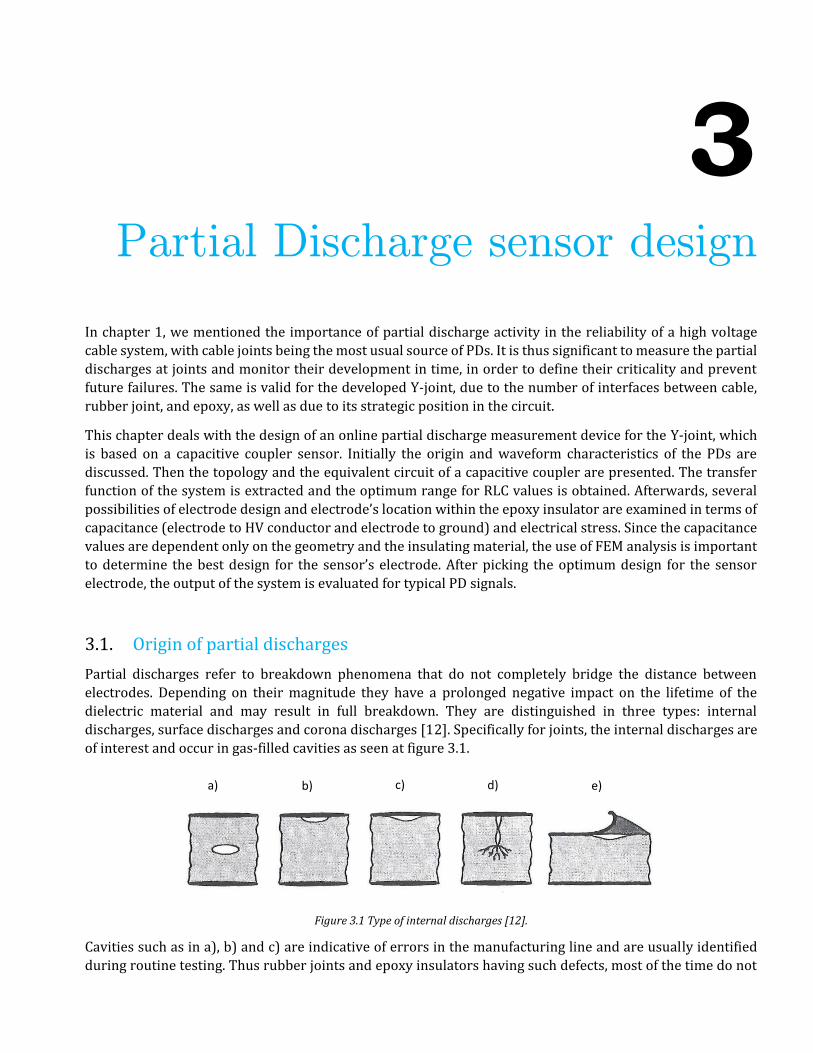
3
3. Partial Discharge sensor design
In chapter 1, we mentioned the importance of partial discharge activity in the reliability of a high voltage
cable system, with cable joints being the most usual source of PDs. It is thus significant to measure the partial
discharges at joints and monitor their development in time, in order to define their criticality and prevent
future failures. The same is valid for the developed Y-joint, due to the number of interfaces between cable,
rubber joint, and epoxy, as well as due to its strategic position in the circuit.
This chapter deals with the design of an online partial discharge measurement device for the Y-joint, which
is based on a capacitive coupler sensor. Initially the origin and waveform characteristics of the PDs are
discussed. Then the topology and the equivalent circuit of a capacitive coupler are presented. The transfer
function of the system is extracted and the optimum range for RLC values is obtained. Afterwards, several
possibilities of electrode design and electrode’s location within the epoxy insulator are examined in terms of
capacitance (electrode to HV conductor and electrode to ground) and electrical stress. Since the capacitance
values are dependent only on the geometry and the insulating material, the use of FEM analysis is important
to determine the best design for the sensor’s electrode. After picking the optimum design for the sensor
electrode, the output of the system is evaluated for typical PD signals.
3.1. Origin of partial discharges
Partial discharges refer to breakdown phenomena that do not completely bridge the distance between
electrodes. Depending on their magnitude they have a prolonged negative impact on the lifetime of the
dielectric material and may result in full breakdown. They are distinguished in three types: internal
discharges, surface discharges and corona discharges [12]. Specifically for joints, the internal discharges are
of interest and occur in gas-filled cavities as seen at figure 3.1.
Figure 3.1 Type of internal discharges [12].
Cavities such as in a), b) and c) are indicative of errors in the manufacturing line and are usually identified
during routine testing. Thus rubber joints and epoxy insulators having such defects, most of the time do not
a) b) c) d) e)

32 Partial Discharge sensor design
reach the installation site. Cavities such as d) or e) may be caused during installation. For instance, if the end
of the cable’s semiconductive layer is longer (or shorter) than it should be, then it will not be properly
shielded from the joint’s electrode ring. This will cause field enhancement, leading to electrical treeing and
PDs as in case d). Furthermore, an improper pealing or sanding of the cable’s insulation can result in cavities
at the interface of the two materials such as in case e). The cavity is then stressed by the tangential electrical
field leading to PDs due to electrical treeing along the interface.
The field strength in such cavities can be calculated by formulas or determined by FEA for complex
geometries. Breakdown occurs when it reaches the ignition field strength obtained from Paschen’s curve. The
equivalent circuit of internal discharges can be seen at figure 3.2a, where cavity’s capacitance c is in series
with a capacitance b and both in parallel with capacitance c of the unaffected dielectric [12]. When sinusoidal
voltage is applied, the voltage over the cavity Vc is increasing and when the breakdown
Figure 3. 2 a) Equivalent circuit for internal discharges, b) Recurrent discharge phenomenon during AC voltage c) Discharge pattern characteristic for cavities, classic detection.
voltage Ud is reached then discharge takes place and the voltage drops to a residual voltage V. The voltage
increases again and the same process is repeated giving a pattern stable at a 50 Hz time base (figure 3.2b).
The discharge pattern can persist even when the voltage drops below the inception voltage.
3.2. Measuring partial discharges
The measurement of the partial discharges is based on measuring the charge displacement at the leads of the
sample via an impedance Z [12]. The magnitude of the discharge is defined as the charge displacement q and
is expressed in picocoulombs. It should be noted that this quantity is related to the discharge but is not an
exact representation of the discharge itself, as the shape of the pulse depends on the circuit parameters [12].
Nevertheless, this is an accepted definition of the discharge intensity as it is directly related to the energy
dissipated in a discharge and the physical size(volume) of the discharge.
When dealing with PD measurement, it is important to mention some important definitions as described in
the IEC-60270 standard for conventional detection [18]:
Partial discharge pulse: A current or voltage pulse that results from a partial discharge occurring in the test object.
a) b) c)

33 Partial Discharge sensor design
Apparent charge q of a PD pulse: is that charge which, if injected within a very short time between the terminals of the test object in a specified test circuit, would give the same reading on the measuring instrument as the PD current pulse itself. The apparent charge is usually expressed in pC.
Phase angle φi and time ti of occurrence of a PD pulse: φi = 360(ti/T)
Pulse repetition frequency N: number of PD pulses per second, in case of equidistant pulses.
Background noise: signals detected during PD tests, which do not originate from the test object.
Sensitivity of the detection circuit: is the smallest discharge impulse that can just be distinguished from background noise. It is measured in pC and the smaller it is the better the sensitivity.
Partial discharge measuring system: can be divided into the subsystems: coupling device, transmission system (for example, connecting cable or optical link) and measuring instrument. An example can be seen at figure 3.3.
Coupling device: The coupling device is an integral part of the measuring system and test circuit, with components specifically designed to achieve the optimum sensitivity with a specific test circuit. Different coupling devices may thus be used in conjunction with a single measuring instrument. The coupling device is usually an active or passive four-terminal network (quadripole) and converts the input currents to output voltage signals. These signals are transmitted to the measuring instrument by a transmission system. The frequency response of the coupling device, defined by output voltage to input current, is normally chosen at least so as to effectively prevent the test voltage frequency and its harmonics from reaching the instrument.
Transfer impedance Z(f): ratio of the output voltage amplitude to a constant input current amplitude, as a function of frequency f , when the input is sinusoidal.
Lower and upper limit frequencies f1 and f2 : frequencies at which the transfer impedance Z(f ) has fallen by 3 dB from the peak pass-band.
Midband frequency: is defined by fm= (f1+f2)/2
Bandwidth: Is defined by Δf= f2-f1
Figure 3.3 Typical arrangement of a wideband PD measuring system.
3.2.1. General requirements of a PD measuring system.
The magnitude and shape of the PD pulses depends on many factors, such as the type of defect, the age of the
cavity, to volume of the cavity, the attenuation during its travel time etc. For instance, in virgin cavities
streamer breakdown occurs, resulting in very short time-to-breakdown in the range of 1 to 10 ns (for 0.1-1
mm cavity depth). On the other hand, in aged cavities Townsend breakdown takes place and the resulting
pulses with longer width (80 ns to 0.8 μs) and lower height [12]. Similar variability in pulse waveform may

34 Partial Discharge sensor design
be observed among different type of defects. Consequently the frequency content of the PD signals arriving
at the sensor’s measuring impedance Zm, varies.
Furthermore, the PD pulses are very small in amplitude and are superposed on the 50 Hz signal which is of a
many kilovolts. Thus, the measuring system must extract
from a high energy signal the details of a very weak signal.
While doing this, signals that are not related to PD activity
must be supressed. The latter is usually the case in on-line
measurements where the network interference is quite
significant.
In general, a PD measurement device must be selective in the
frequency domain. It must thus work as a filter that can
successfully isolate the wanted PD signal from the 50Hz. It
must also have very good sensitivity allowing very small PD
signals to be detected from background noise. The output
signal must be a good representation of all kind of PD pulses,
giving a good estimation of their apparent charge. In figure
3.4c we can see the frequency characteristics of such a
measuring system.
Once the measured signal is obtained, several methods exist
to estimate the charge of the pulse. Three of the most
fundamental methods are based on analysis of a) the signal
in time domain, b) the signal in frequency domain and c) analysis of the impulse response of quashi
integration band pass filters(QI-BPF) [27]. According to [27], in time domain the integral of the measured
pulse y(t) can be related with the integral of the current pulse (i.e. the charge Q) through the property of
convolution. Through this identity the peak of the integral of the measured signal approximates the pulse
charge Q. In frequency domain, it is possible to estimate the charge Q directly from the peak of the low
frequency components of y(t), via spectral analysis. For both methods the charge Q is best approximated
when the lower cut-off frequency of the measuring system is small. In a QI-BPF the charge Q is proportional
to the peak value of the response of the band-pass filter. According to [27] charge determination methods
based on frequency-domain or impulse responses of QI-BPFs give less errors than time-domain methods.
3.2.2. Capacitive coupler.
As already mentioned, this chapter will deal with the design of a PD
measurement device realized by means of a capacitive coupler. Capacitive
couplers have been widely used in joints, cross-bonding cable joints and
cable terminations achieving good sensitivity and employ a method for
integrating PD sensors in cable accessories [19]. The equivalent circuit is
shown at figure 3.5.
The sensor’s electrode will be embedded in the body of the Y-joint’s epoxy
insulator. The geometry of this electrode will determine the capacitance C1
to the energized part (the conductor in our case). Of course the geometry of
the electrode affects also the capacitance C2 to ground. For finding both
capacitances we will utilize the capabilities of the finite element analysis
technique. More specifically, various electrode designs will be simulated
Figure 3.4 a) typical harmonic and continuous interference spectrum on-site , b) frequency spectra of PD
current pulses, c) Bandpass charecteristic of PD measurement systems.
Figure 3.5 Equivalent circuit of capacitive coupler.
Surge
arrestor

35 Partial Discharge sensor design
using the electrostatic module of COMSOL Multiphysics. The analytical method for calculating those
capacitances is presented in paragraph 3.3.
Depending on the values of the capacitances C1 and C2, the values of the inductor L and resistor R will be
selected in order to achieve the best filter characteristics. The transfer function and input impedance of the
coupler is given below:
𝐻(𝑠) =𝑠4(𝑅𝐿)2𝐶1𝐶2 + 𝑠3𝑅𝐿2𝐶1 + 𝑠2𝑅2𝐿𝐶1
𝑠4(𝑅𝐿)2𝐶2(𝐶1 + 𝐶2) + 𝑠3𝑅𝐿2(2𝐶2 + 𝐶1) + 𝑠2[𝑅2𝐿(𝐶1 + 𝐶2) + 𝐿2] + 𝑠2𝑅𝐿 + 𝑅2 (3.1)
𝑍𝑖𝑛𝑝𝑢𝑡 =𝑅 − 𝜔2𝑅𝐿𝐶2 + 𝑗 ∙ 𝜔𝐿(𝑅 + 1)
−𝜔2𝐿𝐶1 + 𝑗 ∙ 𝜔𝑅𝐶1(1 − 𝜔2𝐿𝐶2) (3.2)
There are three requirements for a high performance capacitive coupler: High input impedance, High
bandwidth and low power frequency signal (50/60Hz) at the measuring point [19].
50Hz signal attenuation
One of the main tasks of this filter is to eliminate the 50Hz (or 60Hz) power frequency signal from the
measured signal. This means that a 50Hz sinusoidal waveform of many kV of amplitude must be reduced to
less than 0.1mV. In our case the maximum amplitude of the power frequency signal at the input is:
𝑈0√2 = 36√2 = 50,91 𝑘𝑉𝑝
Thus, the desired minimum attenuation at 50Hz is :
20 log10
𝑉𝑜𝑢𝑡
𝑉𝑖𝑛= 20log10
0.1 ∙ 10−3
50.91 ∙ 103= −174.1 𝑑𝐵
Cut-off frequencies
The bandwidth of the coupler is of paramount importance. While the 50Hz signal and its harmonics must be
eliminated, the higher frequencies of a PD signal shall pass intact. If the lower cut-off frequency of the filter
is increased, then the pulse shape of the PD signal is distorted by creating an oscillation and showing a pulse
with polarity reversal [19]. This polarity change tends to cancel the area of the PD pulse making it more
difficult for the charge evaluation by integrating methods [19]. Furthermore, the sensitivity is reduced when
low cut-off frequency is increased. This is because less frequencies are picked up and the peak value of the
pulse is lower. Depending also on the frequency spectrum of the pulse, slow and fast PD pulses are affected
in different scales when the bandwidth is lower.
In the IEC 60270 standard, the bandwidth for conventional wideband PD measurement devices is from 30
kHz and 500kHz. For non-conventional PD measurements, as in the case of on-line PD monitoring systems,
this bandwidth can be from 10 kHz to 100 MHz.
Furthermore, the flat response of the filter is desired to have an attenuation close to 0dB. If this is not possible,
then amplifiers must be included in the circuit. Typical amplifiers can reach up to a maximum of 20 dB at a
selected bandwidth.
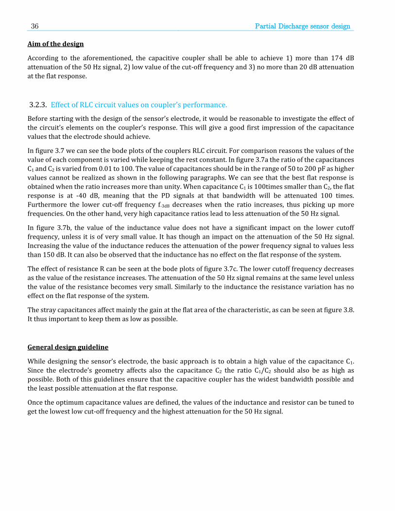
36 Partial Discharge sensor design
Aim of the design
According to the aforementioned, the capacitive coupler shall be able to achieve 1) more than 174 dB
attenuation of the 50 Hz signal, 2) low value of the cut-off frequency and 3) no more than 20 dB attenuation
at the flat response.
3.2.3. Effect of RLC circuit values on coupler’s performance.
Before starting with the design of the sensor’s electrode, it would be reasonable to investigate the effect of
the circuit’s elements on the coupler’s response. This will give a good first impression of the capacitance
values that the electrode should achieve.
In figure 3.7 we can see the bode plots of the couplers RLC circuit. For comparison reasons the values of the
value of each component is varied while keeping the rest constant. In figure 3.7a the ratio of the capacitances
C1 and C2 is varied from 0.01 to 100. The value of capacitances should be in the range of 50 to 200 pF as higher
values cannot be realized as shown in the following paragraphs. We can see that the best flat response is
obtained when the ratio increases more than unity. When capacitance C1 is 100times smaller than C2, the flat
response is at -40 dB, meaning that the PD signals at that bandwidth will be attenuated 100 times.
Furthermore the lower cut-off frequency f-3dB decreases when the ratio increases, thus picking up more
frequencies. On the other hand, very high capacitance ratios lead to less attenuation of the 50 Hz signal.
In figure 3.7b, the value of the inductance value does not have a significant impact on the lower cutoff
frequency, unless it is of very small value. It has though an impact on the attenuation of the 50 Hz signal.
Increasing the value of the inductance reduces the attenuation of the power frequency signal to values less
than 150 dB. It can also be observed that the inductance has no effect on the flat response of the system.
The effect of resistance R can be seen at the bode plots of figure 3.7c. The lower cutoff frequency decreases
as the value of the resistance increases. The attenuation of the 50 Hz signal remains at the same level unless
the value of the resistance becomes very small. Similarly to the inductance the resistance variation has no
effect on the flat response of the system.
The stray capacitances affect mainly the gain at the flat area of the characteristic, as can be seen at figure 3.8.
It thus important to keep them as low as possible.
General design guideline
While designing the sensor’s electrode, the basic approach is to obtain a high value of the capacitance C1.
Since the electrode’s geometry affects also the capacitance C2 the ratio C1/C2 should also be as high as
possible. Both of this guidelines ensure that the capacitive coupler has the widest bandwidth possible and
the least possible attenuation at the flat response.
Once the optimum capacitance values are defined, the values of the inductance and resistor can be tuned to
get the lowest low cut-off frequency and the highest attenuation for the 50 Hz signal.

37 Partial Discharge sensor design
Figure 3.6 Bode diagrams of capacitive coupler showing the effect of a) capacitance ratio, b) inductor and c) resistance.
101
102
103
104
105
106
107
108
109
-200
-180
-160
-140
-120
-100
-80
-60
-40
-20
0
R=250Ω , L=5mH, C2=50pF
Frequency (Hz)
20lo
g(V
out/V
in)
[d
B]
C1=0.01*C
2
C1=0.1*C
2
C1=C
2
C1=10*C
2
C1=100C
2
101
102
103
104
105
106
107
108
109
-200
-180
-160
-140
-120
-100
-80
-60
-40
-20
0
R=250Ω , C2=50pF, C
1=5pF
Frequency (Hz)
20lo
g(V
out/V
in)
[d
B]
L=0.001*5mH
L=0.01*5mH
L=0.1*5mH
L=5mH
L=10*5mH
L=100*5mH
101
102
103
104
105
106
107
108
109
-200
-180
-160
-140
-120
-100
-80
-60
-40
-20
0
L=5mH, C2=50pF, C
1=5pF
Frequency (Hz)
20lo
g(V
out/V
in)
[d
B]
R=0,25Ω
R=25Ω
R=250Ω
R=0,5kΩ
R=2,5kΩ
R=5kΩ
c)
b)
a)
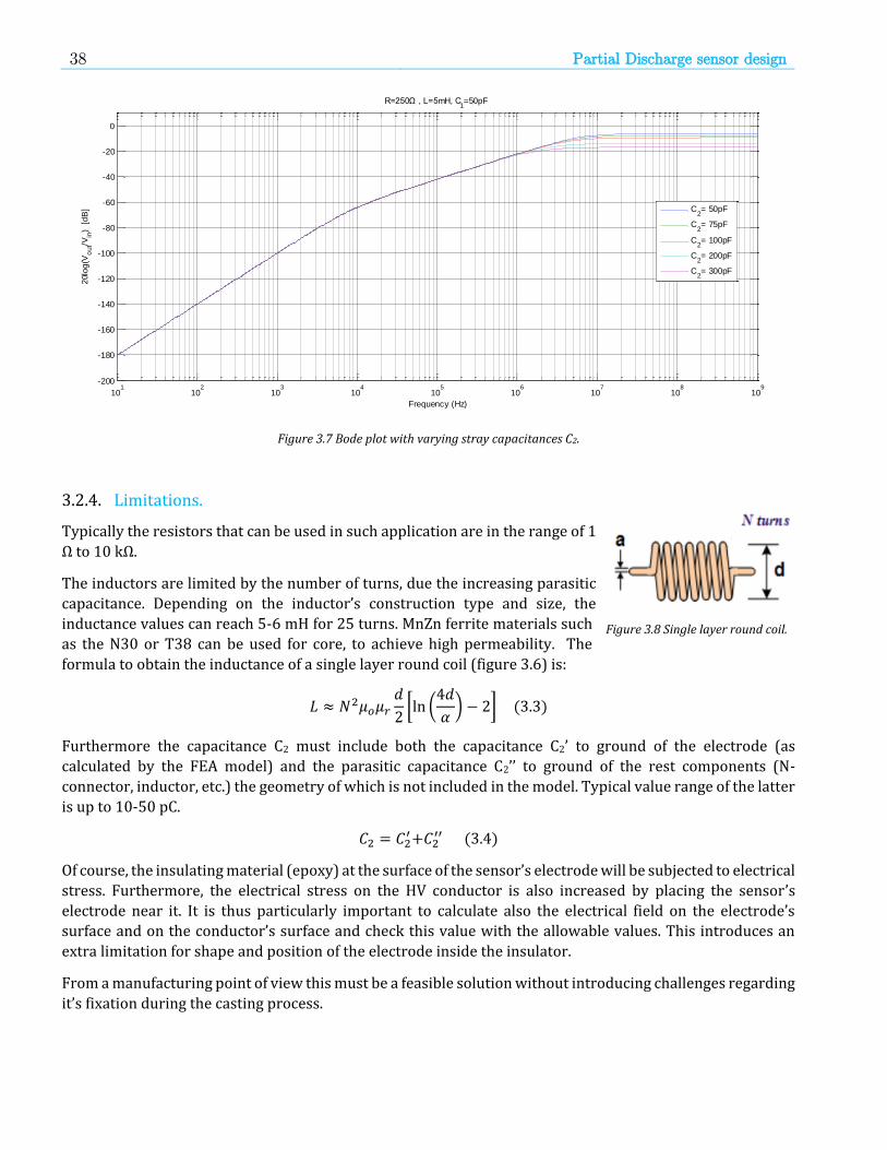
38 Partial Discharge sensor design
Figure 3.7 Bode plot with varying stray capacitances C2.
3.2.4. Limitations.
Typically the resistors that can be used in such application are in the range of 1
Ω to 10 kΩ.
The inductors are limited by the number of turns, due the increasing parasitic
capacitance. Depending on the inductor’s construction type and size, the
inductance values can reach 5-6 mH for 25 turns. MnZn ferrite materials such
as the N30 or T38 can be used for core, to achieve high permeability. The
formula to obtain the inductance of a single layer round coil (figure 3.6) is:
𝐿 ≈ 𝑁2𝜇𝑜𝜇𝑟
𝑑
2[ln (
4𝑑
𝛼) − 2] (3.3)
Furthermore the capacitance C2 must include both the capacitance C2’ to ground of the electrode (as
calculated by the FEA model) and the parasitic capacitance C2’’ to ground of the rest components (N-
connector, inductor, etc.) the geometry of which is not included in the model. Typical value range of the latter
is up to 10-50 pC.
𝐶2 = 𝐶2′+𝐶2
′′ (3.4)
Of course, the insulating material (epoxy) at the surface of the sensor’s electrode will be subjected to electrical
stress. Furthermore, the electrical stress on the HV conductor is also increased by placing the sensor’s
electrode near it. It is thus particularly important to calculate also the electrical field on the electrode’s
surface and on the conductor’s surface and check this value with the allowable values. This introduces an
extra limitation for shape and position of the electrode inside the insulator.
From a manufacturing point of view this must be a feasible solution without introducing challenges regarding
it’s fixation during the casting process.
101
102
103
104
105
106
107
108
109
-200
-180
-160
-140
-120
-100
-80
-60
-40
-20
0
R=250Ω , L=5mH, C1=50pF
Frequency (Hz)
20lo
g(V
out/V
in)
[d
B]
C2= 50pF
C2= 75pF
C2= 100pF
C2= 200pF
C2= 300pF
Figure 3.8 Single layer round coil.

39 Partial Discharge sensor design
3.3. Designing the capacitive coupler’s electrode
It is quite clear that a perfect balance must kept between the goals and limitations that were thoroughly
described in the previous paragraph. The sensor’s electrode in particular, must be ideally shaped and
strategically placed inside the epoxy body. In order to calculate the capacitances C1 and C2’ and the maximum
electrical field at the surface of the electrode, it is necessary to utilize the capabilities offered by the finite
element analysis tools. In this way various shapes of the electrode can be made and added in the 3D geometry
model.
As shown in figure 3.9 the electrode will be placed
inside the body of the insulator. Due to the
complexity of the geometry, standard formulas for
calculating the field and capacitances have not
effect here. Instead the finite element modeling
should be used, and in particular the electrostatic
analysis. The following steps are followed:
a. The 3D shape of the electrode is designed and added to the 3D model of the Y-joint.
b. The electrostatic simulation is run with the electrode boundary set at ground potential.
c. The maximum electrical field at the surface of the electrode is calculated.
d. The capacitances C1 of the electrode to the HV conductor and C2’ of the electrode to the grounded screen of the insulator are calculated. The exact calculation method is presented at Appendix A.
e. The value of the capacitances C1 and C2 is known and the bode diagram can be plotted.
f. The optimum values of R and L are selected, respecting their range given at paragraph 3.2.
g. The electrode is evaluated in terms of electrical field at its surface, 50Hz signal attenuation, lower cutoff frequency, and flat response attenuation.
All aforementioned steps are repeated for each of the electrode arrangements.
3.3.1. Electrode type I - M8 metallic insert.
It would be reasonable to check the possibility of using one of the embedded M8 metallic inserts for such
purpose. From a manufacturing point of view this is quite easy to realize since it is only necessary to strip a
small part of the zinc coating around the insert to isolate it from ground. At figure 3.10 we see the electrode
arrangement inside the simulation model. The M8 insert will be treated as a floating electrode isolated 6 mm
from the zinc coating.
The capacitance of the electrode towards the high voltage and towards the grounded parts is calculated as explained in appendix A:
C1= 0.568pF and C2’=6.15 pF
By adding a parasitic capacitance C2’’=50pF the total capacitance to ground is
𝐶2 = 𝐶2’ + 𝐶2’’ = 56.15 𝑝𝐹
Figure 3.9 Conceptual drawing of the sensor’s electrode embedded in the insulator’s body.
Electrode

40 Partial Discharge sensor design
Figure 3.10 An M8 insert used as PD sensor’s electrode.
We can expect that the attenuation in the flat region of the filter will be high due to the very low capacitance ratio C1 / C2, which is close to 0.01. This is obvious from the bode plot shown at figure 3.11. The filter characteristics are shown at table 3.1. The values for the resistor and inductor are tuned to achieve the best frequency response.
Table 3.1: Capacitive coupler performance - electrode type I
f-3db
[kHz]
Attenuation at flat region
[dB]
Attenuation @ 50 Hz signal
[dB]
Input imp. @50 Hz
[GΩ]
Input imp. @100 ΜΗz
[kΩ]
Vout @
Vin=50,91 kVp
[mV]
281,8 -39.99 -192.95 5,6 2.84 0.011
PD sensor
electrode Ground
electrode HV
electrode
101
102
103
104
105
106
107
108
109
-200
-180
-160
-140
-120
-100
-80
-60
-40
-20
0
R=5kΩ , L=4mH, C1=0.568pF, C
2=51.65pF
Frequency (Hz)
20lo
g(V
out/V
in)
[d
B]
Figure 3.11 Bode plot of capacitive coupler with M8 insert used as sensor's electrode.

41 Partial Discharge sensor design
The coupler gives a very good attenuation of the 50 Hz signal as it reaches 192dB which is much higher than the target of 174 dB. The attenuation though at the flat region is very high, which is not desired. The PD signals at this bandwidth are attenuated by 100 times, making it very difficult for conventional amplifiers to achieve amplification. This is can be attributed mainly to the small surface of the electrode and its relatively long distance from the HV part, resulting in a low capacitance C1 which cannot reach the high stray capacitance value close to 50pF.
The electrical field at the surface of the electrode is shown at figure 3.12. The maximum value is located at the round corners of the insert facing the HV conductor. This value stays below the maximum reference of 0.0876 kV/mm per kV applied (28.5 kV/mm @325 kV BIL), which was introduced in the design of the epoxy insulator at chapter 2.
3.3.2. Electrode type II - Disc plate.
The previous type of electrode, although favourable from a manufacturing and cost point of view, resulted in a very low capacitance C1 which was overshadowed by the total capacitance to ground C2 giving high attenuation at the flat region of the bode diagram. Since C2 is dominated by the parasitic capacitance C2’’, which can be up to 50 pF, the capacitance C1 must achieve values in the order of tens of picocoulombs. For this reason, a special electrode must be designed and be embedded in the epoxy during the casting process.
In order to increase the capacitance C1, the basic approach is to place the electrode closer to the high voltage conductor. This will also reduce the capacitance C2’ to ground. Of course, by placing a metallic surface with almost 0V potential closer to the HV side, will lead to an increase of the electrical field both on the conductor and on the electrode’s surface. Consequently, the main limiting factor in this approach is the maximum allowable electrical field in epoxy.
Figure 3.13 FEM model - Disk plate (D=40 mm) used as PD sensor's electrode.
A favourable spot for placing the electrode, is the “elbow” corner of the insulator, due to the large spacing between the ground and HV conductor. A disc plate of 40 mm diameter is placed at 25 mm distance from the conductor as seen at figure 3.13.
The capacitance of the electrode towards the high voltage and towards the grounded parts is calculated as explained in appendix A:
C1= 4.15pF and C2’=5.69 pF
Figure 3.12 Electrical field on the surface of the sensor's electrode -1000 V applied [kV/mm].
PD sensor
electrode Ground
electrode HV
electrode

42 Partial Discharge sensor design
By adding a parasitic capacitance C2’’=50 pF the total capacitance to ground is
𝐶2 = 𝐶2’ + 𝐶2’’ = 55.69 𝑝𝐹
Figure 3.15 Electrical field on conductor and on the surface of the disc plate (D=100 mm) -1 kV applied [kV/mm]
With this type of electrode the capacitance C1 is almost 10 times higher than that of the M8 insert examined previously. Furthermore, the capacitance C2’ is also reduced. Both will have a positive effect at the frequency response of the coupler. The electrical field on the surface of the conductor and the electrode stay below the reference value as can be seen at figure 3.14.
Another way to increase the capacitance C1 is to increase the electrode’s surface. At figure 3.15 we can see the bode plot for various plate diameters. The positive effect of increasing the diameter is obvious from the decrease of the attenuation at the flat region of the bode diagram. For large diameters though, the capacitance C2’ increases a lot and the ratio C1/C2 reduces. In addition, the electrical field at the conductor’s surface increases when the diameter is increased.
Table 3.2: Capacitive coupler performance - electrode type II
f-3db [kHz]
Attenuation at flat region
[dB]
Attenuation @ 50Hz signal
[dB]
Vout @ Vin=50,91kVp
[mV]
Input imp. @50Hz
[GΩ]
Input impedance @100ΜΗz
[kΩ]
224 -20.3 -170.1 0.161 0.5 0.283
101
102
103
104
105
106
107
108
109
-200
-180
-160
-140
-120
-100
-80
-60
-40
-20
0
Frequency (Hz)
20lo
g(V
out/V
in)
[d
B]
Rplate
=20mm, L=4mH, R=5.5kΩ
Rplate
=30mm, L=4.8mH, R=6kΩ
Rplate
=50mm, L=4mH, R=5.5kΩ
50Hz
Figure 3.14 Bode plot of capacitive coupler with disc plate.

43 Partial Discharge sensor design
The coupler gives a moderate attenuation of the 50 Hz signal as it reaches around 165-175 dB depending on the diameter of the plate. In order to further attenuate the power frequency signal, lower inductance could be chosen with the adverse effect of increasing the lower cutoff frequency. The attenuation at the flat region is at the range of -19 to -23 dB, which is still high but acceptable.
Figure 3.16 Electrical field plot and equipotential lines plot for disc type electrode.
3.3.3. Electrode type III - Coaxial cylindrical insert.
While the option of using a disc plate for the sensor’s electrode increases the capacitance C1 tenfold compared to the M8 option, this is not enough to bring the attenuation at the flat region to reasonable levels. Consequently, the capacitance C1 should increase even more.
An electrode must be designed, that can achieve higher C1 values while keeping the C2’ at low value values. In electrode type II increasing the area of the disc was not such effective, because the distance from HV also increased and the distance to ground decreased. The best option would be an electrode with a large surface at constant distance from the conductor. The best way to achieve that is via a cylindrical geometry. The horizontal leg of the Y-joint is the most appropriate location to place a cylindrical insert. This cylindrical insert could be made out of metallic mesh which is quite common electrode material at the MV industry.
To optimize the size of the cylindrical insert, we will choose for an inner diameter that results in an electrical field at the surface of the conductor close to the maximum reference value (0.0876 kV/mm per kV applied (28.5 kV/mm @325 kV BIL). Using the standard formula for coaxial cylinders we find that for R= 35.9 mm the E-field at the surface of the conductor will be:
𝐸𝑐𝑜𝑛𝑑 =1
20 ln35.920
= 0.0855 [𝑘𝑉
𝑚𝑚] 𝑝𝑒𝑟 𝑎𝑝𝑝𝑙𝑖𝑒𝑑 𝑘𝑉 (3.5)
The cylindrical electrode is designed based on that inner diameter. The edges of the cylinder are given a special profile to avoid field enhancement. The thickness of the cylinder is kept as low as possible (1 mm) to decrease the distance of its outer surface from the grounded coating of the insulator (reduction of the C2’’). The cylinder’s length must be as long as possible to achieve the maximum capacitance. It should be noted though, that large length could bring its edges out of the shield effect provided by the cones’ bases. As a result, the cylinder has a length of 95 mm. For this length the expected capacitance C1 can be approximated from the following formula:
𝐶1 = 2𝜋휀휀0
𝑙
ln𝑅𝑟
= 2𝜋 ∙ 4.5 ∙ 8.854 ∙95 ∙ 10−3
ln35.920
= 40.6 𝑝𝐹 (3.6)
The design and positioning of the sensor’s electrode is shown at figure 3.17.

44 Partial Discharge sensor design
Figure 3.17 FEM model - Coax. cylinder used as PD sensor's electrode.
The maximum electrical field at the surface of the conductor is at 0.083 kV/mm for 1 kV applied voltage (figure 3.18). This is less than the estimated in formula 3.5, due to the finite coaxial geometry of the arrangement. The field at the edges of the cylinder remain below the maximum value.
Figure 3.18 Electrical field on conductor and on the surface of the coaxial sensor -1000V applied [kV/mm].

45 Partial Discharge sensor design
Figure 3.19 Electrical field plot and equipotential lines plot for coaxial cylinder electrode.
The capacitance of the electrode towards the high voltage and towards the grounded boundaries is:
C1= 51.98 pF and C2’=55.25 pF
By adding the parasitic capacitance of C2’’=50pF the total capacitance to ground is:
𝐶2 = 𝐶2’ + 𝐶2’’ = 105.25 𝑝𝐹
The FEM computed capacitance C1 is higher than the one calculated from the previous formula, due to the irregular geometry (larger surface) of the HV conductor and the surface at the rounded edges of the cylinder. The value of C1 is almost 10 times larger than the capacitance obtained with the flat disc electrode. The ratio C1/C2 is now almost 0.5 which is a significant improvement.
Figure 3.20 Bode plot of capacitive coupler with coaxial cylinder electrode.
101
102
103
104
105
106
107
108
109
-200
-180
-160
-140
-120
-100
-80
-60
-40
-20
0
R=3.2 kΩ , L=0.4 mH, C1=51.98pF, C
2=105.25pF
Frequency (Hz)
20lo
g(V
out/V
in)
[d
B]
50Hz

46 Partial Discharge sensor design
This is also clear at figure 3.20 and table 3.3. The attenuation at the flat region is at 9.5 dB or Vout=0.335 Vin at
that bandwidth. The -173.7 dB attenuation of the 50Hz signal is also satisfactory. The lower cutoff frequency
is relatively high but satisfactory for the purpose of online PD measurements.
Table 3.3: Capacitive coupler performance - electrode type III
f-3db
[kHz]
Attenuation at flat region
[dB]
Attenuation @ 50Hz signal
[dB]
Vout @
Vin=50,91kVp
[mV]
Input imp. @50Hz
[GΩ]
Input imp. @100ΜΗz
[kΩ]
467 -9.5 -173.7 0.105 0.062 0.046
Figure 3.21 Bode plot of capacitive coupler with coaxial cylinder electrode - effect of parasitic capacitance.
3.4. Evaluation of electrode designs
In the previous paragraph, several capacitive electrode designs were examined. The following table evaluates these designs in terms of electrical field increase, frequency characteristics, fixation scheme complexity and manufacturing cost. The evaluation score is from 0 to 10, with 10 corresponding to the most favourable result. On figure 3.22 the bode diagrams of each arrangement are plotted.
We can see that the 1st type of electrode is the most preferred arrangement from a manufacturing point of view, since no extra electrode insert is added in the epoxy body and only a local striping of the zinc coating around the base of the M8 insert is necessary. Nevertheless the attenuation at the flat region is very high making it inadequate for the purposes of this application.
The flat disc electrode offers the simplest solution as for adding a separate electrode inside the epoxy body. It can be produced relatively cheaply and fixed by a simple support beam at the corner of the Y-joint insulator. The attenuation at the flat region, although improved compared to the type I, it is high.
The coaxial electrode gives the best frequency response compared to the previous types. Its relatively high capacitance C1 and high ratio C1/C2, gives a less than 10dB attenuation at the flat region. On the other hand it
106
107
108
109
-20
-18
-16
-14
-12
-10
-8
-6
-4
-2
0
Frequency (Hz)
20lo
g(V
out/V
in)
[d
B]
C2''=50pF
C2''=30pF
C2''=10pF
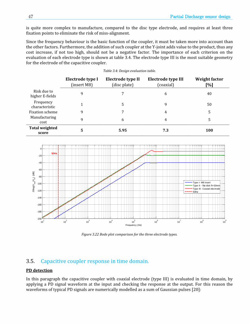
47 Partial Discharge sensor design
is quite more complex to manufacture, compared to the disc type electrode, and requires at least three fixation points to eliminate the risk of miss-alignment.
Since the frequency behaviour is the basic function of the coupler, it must be taken more into account than the other factors. Furthermore, the addition of such coupler at the Y-joint adds value to the product, thus any cost increase, if not too high, should not be a negative factor. The importance of each criterion on the evaluation of each electrode type is shown at table 3.4. The electrode type III is the most suitable geometry for the electrode of the capacitive coupler.
Table 3.4: Design evaluation table.
Electrode type I
(insert M8)
Electrode type II
(disc plate)
Electrode type III
(coaxial)
Weight factor
[%]
Risk due to higher E-fields
9 7 6 40
Frequency characteristic
1 5 9 50
Fixation scheme 9 7 4 5
Manufacturing cost
9 6 4 5
Total weighted score
5 5.95 7.3 100
Figure 3.22 Bode plot comparison for the three electrode types.
3.5. Capacitive coupler response in time domain.
PD detection
In this paragraph the capacitive coupler with coaxial electrode (type III) is evaluated in time domain, by applying a PD signal waveform at the input and checking the response at the output. For this reason the waveforms of typical PD signals are numerically modelled as a sum of Gaussian pulses [20]:
101
102
103
104
105
106
107
108
109
-200
-180
-160
-140
-120
-100
-80
-60
-40
-20
0
Frequency (Hz)
20lo
g(V
out/V
in)
[d
B]
Type I- M8 insert
Type II - flat disk R=50mm
Type III- Coaxial electrode
50Hz
50Hz

48 Partial Discharge sensor design
𝑦 = ∑𝐴𝑖
𝑊𝑖√𝜋/2𝑒
−2(𝑥−𝑋𝑐𝑖
𝑊𝑖)2
𝑛
𝑖=1
(3.7)
where y is the voltage (PU) n is the number of sub-pulse Ai is the amplitude of the sub-pulse (pu*ns) Wi is the width of the sub-pulse (ns) Xci is the x-position of the sub-pulse peak (ns).
Depending on the type of defect, the PD waveform shape changes. In table 3.5 we see the parameters of equation 3.5 and the characteristics of pulses generated from a needle and void type defect. Those are based on real PD measurements of void and needle defects as found in literature [20]. The waveform and frequency content of those PD signals are shown at figure 3.23.
PD pulses generated from the needle defect have a shorter rise time and fall time compared to those generated from the void defect. This results in a narrower bandwidth for the latter (0-150 MHz), whereas most of the signal’s energy is below the 75MHz. Furthermore, for the negative pulse from void defect, the dominating frequencies have much higher amplitude amplitude (0.12pu) than for the other two pulse waveforms.
With such signals the capacitive coupler’s response will be evaluated for pulses with energy concentrated at lower as well as at higher frequencies. The RLC circuit is simulated at OrCAD Capture CIS as shown at figure 3.25. The response of the system for all three types of PD pulses is shown at figure 3.26.
From the figures we see that the output signals are attenuated compared to the input pulses. This is expected due to the non-zero flat response of the bode diagram. Nevertheless the attenuation is only 0.33 of the input and can be amplified if necessary. Furthermore, most important is the fact that the shape of the pulses is not distorted at the output even for the negative pulse which has most of the energy concentrated at low frequencies. This proves that the 467 kHz lower cut-off frequency is not limiting the
Positive
pulse needle defect
Positive pulse void
defect
Negative pulse void
defect
A1 [pu*ns] 2.44 9.73 -7.66
A2 [pu*ns] 2.54 -3.53 -2.66
A3 [pu*ns] -1.65 1.60 -6.14
A4 [pu*ns] -0.72 - -
A5 [pu*ns] 0.55 - -
W1 [ns] 1.91 7.04 6.58
W2 [ns] 2.65 18.3 8.15
W3 [ns] 1.97 6.03 36.8
W4 [ns] 2.23 - -
W5 [ns] 2.78 - -
Xc1 [ns] 40.3 44.4 35.8
Xc2 [ns] 44.8 50.2 48.9
Xc3 [ns] 45.8 59.7 66.0
Xc4 [ns] 49.4 - -
Xc5 [ns] 55.1 - -
Rise time (10%-90%)
[ns] 0.8 5 4.8
Fall time
(10%-90%) [ns]
1.2 4.8 36
Duration time
[ns] 22 40 97
Bandwidth
[MHz] 0-600 0-150 0-150
Table 3.5: Characteristics of typical defect PD pulses.
49 Partial Discharge sensor design
bandwidth of the coupler for picking such PD pulses. Of course PD pulses with dominating frequencies of a few kHz will be distorted, thus the sensor applies purely for HF partial discharge detection.
Figure 3.23 Waveform of PD pulses.
Figure 3.24 Frequency spectrum of PD pulses.
Figure 3.25 Capacitive couplers simulation circuits at OrCAD Capture CIS a) PD pulse input and b) Power frequency input.
0 2 4 6 8 10 12 14 16 18 20 22 24 26 28 30-0.4
-0.3
-0.2
-0.1
0
0.1
0.2
0.3
0.4
0.5
0.6
0.7
0.8
0.9
1
1.1
1.2a) Positive PD pulse from needle type defect.
t [ns]
volt
ag
e [
pu]
0 5 10 15 20 25 30 35 40 45 50 55 60 65 70-0.2
-0.1
0
0.1
0.2
0.3
0.4
0.5
0.6
0.7
0.8
0.9
1
1.1
1.2b) Positive PD pulse from void type defect.
t [ns]volt
ag
e [
pu]
0 10 20 30 40 50 60 70 80 90 100 110 120 130-1
-0.9
-0.8
-0.7
-0.6
-0.5
-0.4
-0.3
-0.2
-0.1
0
0.1c) Negative PD pulse from void type defect.
t [ns]
volt
ag
e [
pu]
0 50 100 150 200 250 300 350 400 450 500 550 6000
0.005
0.01
0.015
0.02
0.025
0.03
0.035
0.04a) Positive PD pulse from needle type defect
Frequency (MHz)
|P(f
)|
0 20 40 60 80 100 120 140 160 180 2000
0.01
0.02
0.03
0.04
0.05
0.06
0.07
0.08
0.09b) Positive PD pulse from void type defect
Frequency (MHz)
|P(f
)|
0 20 40 60 80 100 120 140 160 180 2000
0.02
0.04
0.06
0.08
0.1
0.12
0.14c) Negative PD pulse from void type defect
Frequency (MHz)|P
(f)|
GND_0
0
C3
51.98pF
R1
3.2k
Vin
Vout
L1
0.4mH
0V
C4
105.25pF
V1
FILE
GND_0
0
C3
51.98pF
R1
3.2k
Vin
L1
0.4mH
Vout C4
105.25pF
V1
FREQ = 50VAMPL = 50.91kVOFF = 0
AC =
a) b)

50 Partial Discharge sensor design
Figure 3.26 Input and output PD signals from OrCAD Capture CIS simulation. a) Positive pulse from needle defect, b) positive pulse from void defect and c) negative pulse from void defect.
Time
20ns 30ns 40ns 50ns 60ns 70ns 80nsV(Vin)
0.5V
1.0V
-0.1VSEL>>
V(Vout)
0V
200mV
350mV
Time
0s 20ns 40ns 60ns 80ns 100nsV(Vin)
-1.0V
-0.5V
0.0V
V(Vout)
-200mV
-100mV
0V
-350mVSEL>>
Time
30ns 35ns 40ns 45ns 50ns 55ns 60ns 65nsV(Vin)
0V
0.5V
1.0V
SEL>>
V(Vout)
0V
200mV
350mV
a)
b)
c)

51 Partial Discharge sensor design
Power frequency attenuation
As already mentioned, one of the most important tasks of the sensor is to eliminate the superimposed power frequency signal. The -173 dB attenuation that was calculated previously is also evident at figure 3.27, at which the 50.91 kVp powerfrequency input signal is reduced to only 0,1 mVp.
Figure 3.27 Input and output 50Hz signals obtained from OrCAD Capture CIS simulation.
Lightning impulse
For safety reasons it would be reasonable to check the response of the coupler in case of 1.2/50 μs lightning impulse. Due to the short rise time and high amplitudes (325 kV peak) the energy of such pulse is concentrated at the range of a few kHz. The attenuation of the coupler in such frequencies is not enough to quench such high amplitudes. In figure 3.28 we see that a 30 kVp oscillation of a few μs occurs at the output of the coupler. This could prove dangerous for both equipment and personnel, therefore a surge arrestor (spark gap) must be placed in parallel to the RLC impedance, as shown at figure 3.5.
Figure 3.28 a) Frequency spectrum of lightning impulse and b) waveform of impulse at the input and output of the capacitive coupler.
Time
20ms 30ms 40ms 50ms 60ms 70ms 80ms 90ms 100msV(Vin)
0V
50KV
-70KVSEL>>
V(VOUT)
-100uV
0V
100uV
0 20 40 60 80 100 120 140 160 180 2000
1
2
3
4
5
6
7x 10
4
Frequency (kHz)
|P(f
)|
Time
0s 50us 100us 150us 200usV(Vout)
-40KV
0V
40KV
SEL>>
V(Vin)0V
100KV
200KV
300KV
a) b)

52 Partial Discharge sensor design
3.6. Conclusions
In this chapter we examined the possibility of integrating a partial discharge sensor in the epoxy insulator of the Y-joint. This sensor will be realized by means of a capacitive coupler, the electrode of which is specifically designed in order to achieve the best frequency characteristics and at the same time keep within limits the electrical field in epoxy. Several design arrangements have been simulated with the main goal of achieving a high capacitance C1, which corresponds to the capacitance between the electrode and the inductor. The option of using one of the M8 inserts will not work for the purpose of the sensor as the C1 capacitance is very low and also much smaller than the capacitance towards ground C2. The option of using a flat disc close to the aluminium conductor will not result in good frequency behaviour since the attenuation at the HF region is high at -20 dB. The most feasible solution is a coaxial cylindrical insert placed around the horizontal leg of the conductor. The insert can be realised by means of stainless steel mesh and common resistor and inductor are used to connect it to ground, completing the RLC circuit. This arrangement resulted in high capacitance C1 and relatively low C2 resulting in low attenuation at the HF region (-9 dB).
The coupler is able to successfully detect high frequency partial discharges originating from typical cable
defects, such as voids and protrusions. Furthermore, the 50 Hz high power signal is quenched to very low
levels. Both prove the satisfactory frequency behaviour of the sensor which can be used for the online
monitoring of partial discharges.

4 4. Thermal Analysis
The ability of calculating accurate current ratings for the components of high voltage circuits, is vital for the
design and operation of the electricity networks. For a cable system, comprised of the cables and the
accessories, the rating is usually derived by the cables alone, assuming that the accessories operate at a lower
or equivalent temperatures due to the increased core to core spacing at the joint position compared to the
rest cable arrangement [28]. With this assumption the joint bay will not become a limiting factor on the circuit
rating [29]. Nevertheless, the thermal rating itself is a complex procedure affected by many factors, and there
are loading conditions that might bring the thermal design of the accessories to their limits. Such high loading
conditions may be encountered at wind farms, as according to a CIGRE study [30], these can occur in both
sustained wind periods of several days as well as intermittently during variable wind conditions.
For this reason, it would be reasonable to investigate the thermal behaviour of the 72 kV Y-joint under both
steady and time dependent situations. For two cable joints, relatively quick and analytical techniques exist
based on electrical analogues to thermal systems. These take advantage of the axial symmetry and represent
different materials and their resistances with simple capacitance and admittance networks [31]. However,
due to the practical limitations of this method and the development of powerful computers and sophisticated
software, Finite Element Analysis modeling techniques have become the most appropriate tool for rating
calculations. Especially, for detailed 3-dimensional geometry, such as the Y-joint, consisting of many
materials and involving more than one heat production and heat transfer phenomena, the FEA method is
ideal. Nevertheless, due to practical restrictions associated with computation power and memory,
assumptions must be made in the FEM model in order to save simulation time, especially for time dependent
studies.
In this chapter, the current-carrying capability, of the Y-joint is examined via FEA. Initially, a 2D model for
thermal analysis of a 32 kV XLPE cable is made, and the results are compared with real measurements to
validate the boundary conditions and the material properties. Then the ampacity and thermal parameters
(i.e. thermal time constants and thermal resistance) of four 60 kV XLPE cables are calculated. Then a 3D
model of the Y-joint is simulated and the same parameters are extracted and compared to the 60 kV cables.
At last the thermal behaviour of the Y-joint during IEC heat cycle is examined, and the appropriate 60 kV
cable is chosen. Since the Y-joint is a three cable joint, it could also serve as a two cable joint with one end
properly terminated. Consequently, every simulation will be performed three times, as three paths exist for
the maximum current to pass. At the end, conclusions are drawn and points are highlighted for the system’s
design engineering, when securing the thermal limits of the Y-joint in service operation.

54 Thermal analysis
4.1. Heat sources in a HV system
There are three principle losses that generate heat within an AC cable system, namely the joule losses at the
conductor, the dielectric losses and the sheath/armour losses. Another heat energy source could be the sun
or other radiative source, when the system is installed in air and directly exposed to it.
4.1.1. Conductor losses
These are ohmic losses (Watt) and are equal to:
𝑃𝑐 = 𝐼2𝑅(𝜃𝑐) (4.1)
where I = current carried by the conductor (A)
R(θc) = omhic AC resistance of the conductor at θc°C (Ω)
θc = is the temperature of the conductor (°C)
The AC resistance is different from the DC resistance, due to the alternating nature of the circulating currents. These cause a non-homogeneous current distribution inside the conductor, due to two independent effects known as the “skin effect” and the “proximity effect”. The first one is considered self-induced by the magnetic field of current flowing in the conductor itself. It forces the current to concentrate on the surface of the conductor, thus increasing the effective resistance. The second one is caused by the magnetic field generated by adjacent current carrying conductors and it also increases the effective resistance. Both effects are mathematically treated into factors that can be multiplied with the DC resistance value. Furthermore, the DC resistance, and more precisely the specific resistivity of metals (like copper and aluminum) is increasing with temperature. The temperature coefficient and the specific resistivity at known temperature (usually 20°C) are the material dependent coefficients of this effect. All the aforementioned phenomena are taken into account in the following formula for calculating the AC resistance of a conductor [32] :
𝑅(𝜃𝑐) = 𝑅′(𝜃𝑐)(1 + 𝑦𝑠 + 𝑦𝑝) (4.2)
𝑅′ =1.02∗106
𝐴𝜌20[1 + 𝛼20(𝜃𝑐 − 20)] (4.3)
where ρ20 = specific resistivity at 20°C (Ω)
α20 = the temperature coefficient at 20°C (1/°C)
θc = is the temperature of the conductor (°C)
A = conductor area (mm2)
ys = the skin effect factor
yp = the proximity effect factor
The skin and proximity factors are computed from the following expressions [32]:
𝑦𝑠 =𝑥𝑠
4
0.8𝑥𝑠4+192
(4.4) , 𝑥𝑠2 =
8𝜋𝑓
𝑅′ 10−7𝑘𝑠 (4.5)
𝑦𝑝 = 𝐹𝑝(𝑑𝑐
𝑠)2 [0.312 (
𝑑𝑐
𝑠)2+
1.18
𝐹𝑝+0.27] (4.6) , 𝐹𝑝 =
𝑥𝑝4
0.8𝑥𝑝4+192
(4.7) , 𝑥𝑝2 =
8𝜋𝑓
𝑅′ 10−7𝑘𝑝 (4.8)
where ks = 1 for round compact aluminium
kp = 1 for round compact aluminium
s = spacing between conductors of the same circuit (mm)
dc = conductor diameter (mm)

55 Thermal analysis
The resistance is both material dependent (specific resistivity/conductivity) and geometry dependent (it increases with the length and decreases with area). For this reason, only the specific resistivity of the material is necessary for the FEA model. The resistance can be than computed from the FEM model for any geometry. For the DC joule heating model, the conductor’s specific resistivity is:
𝜌(𝜃𝑐) = 𝜌20[1 + 𝛼20(𝜃𝑐 − 20)](1 + 𝑦𝑠 + 𝑦𝑝) (4.9)
For aluminum, typical values specific resistivity and temperature coefficient are 2.8264*10-8 (Ωm) and 0.00403 K-1. At temperature of 95°C the value of skin effect for the joint’s conductor factor is of ys = 0.0858.
With these formulas we can estimate the losses in the Y-joint assuming the longest current path of L=1273mm and smallest conductor diameter of dc=40 mm. To account for proximity effect the distance between the two axis of the joint is considered (s=220 mm). The proximity factor is then yp = 0.00094.
Using equation 4.1 the conductor losses for 2000 A circulating in the Y-joint are:
𝑃𝑐 = 166.59 𝑊
4.1.2. Dielectric losses
These are losses generated inside the insulation material and are due to the imperfection of the dielectric causing a small current Ir which is in phase with Uo. The dielectric losses (Watt per phase) are:
𝑃𝑑 = 2𝜋𝑓𝐶 𝑈02 𝑡𝑎𝑛𝛿 (4.10)
where f = frequency (Hz)
Uo = phase voltage (V)
C = capacitance phase to ground (F)
Tanδ = dielectricl loss angle
In the previous chapter, we calculated the capacitance of the Y-joint which is 0.58nF. From material data the dielectric loss angle for epoxy is tanδ=0.009. Hence, from formula 4.10 and for Uo=36 kV , f=50 Hz, the dissipated power due to dielectric losses in the Y-joint is :
𝑃𝑑 = 2.12 𝑊
The dielectric losses are only 1.2% of the conductor losses and can be neglected when computational time of the model increases.
4.1.3. Sheath and armour losses
Sheath losses
Sheath losses are current dependent and can be distinguished into losses due to circulating currents that flow
in the sheaths of single core cables if the sheaths are bonded at two points, and losses due to eddy currents,
which circulate radially (skin effect) and azimuthally (proximity effect) [32]. From the IEC60287 standard
sheath losses can be calculated and taken as a factor of the conductor losses:
𝑃𝑠 = 𝜆1𝑃𝑐 (4.11)

56 Thermal analysis
𝜆1 = 𝜆1′ + 𝜆1
′′ (4.12)
where λ1’= loss factor due to circulating currents
λ1’’= loss factor due to eddy currents
The cable sheaths must be earthed for safety reasons. Sheath losses in single core cables depend mainly on
the sheath bonding arrangement which can either single-point, solid or cross bonding. For single core cables
with sheaths bonded at both ends of an electrical section, only losses due to circulating currents are
considered [32]. In case of cross or single point bonding, the circulating currents are eliminated and the losses
are caused mainly by eddy currents. In the latter case the current carrying capacity is increased.
In my simulations the sheath losses shall originate only by eddy currents, assuming a single point or cross
bonding arrangement. This way the Y-joint can be subjected to the maximum possible current.
Armor losses
Losses in armouring can also be categorized depending on the cable type, the armour material and the
installation conditions [32]. For single core cables the magnetic properties of the armour material play an
important role. If magnetic armour is used the losses due to eddy currents and hysteresis would be very high.
For this reason nonmagnetic material is used and the armour losses are taken into account in the sheath
losses, as parallel combination of the sheath and armour resistances.
In the simulations that follow, armour is not included in the cable design and thus sheath losses are only
considered.
4.2. Heat transfer
The losses generated inside a cable system produce heat which is dissipated into the surrounding medium
through the insulation and the other layers (metal sheath, servings, protection casing for accessories etc.).
The ampacity of a cable or a cable accessory is the maximum current that the conductor can carry
continuously without exceeding the temperature limits for the insulating components, usually defined by the
relevant standards. In order calculate the ampacity, the main heat transfer mechanisms must be identified
and the relevant heat transfer equations solved.
4.2.1. Heat transfer mechanisms.
Heat transfer is defined as the movement of energy due to a difference in temperature. The main mechanisms
for heat transfer are:
Conduction - Depending on the media, heat conduction can happen via different mechanisms, such as lattice vibrations, collision or oscillation of the molecules and electron movement [33]. Typical for heat conduction is that the heat flux is proportional to the temperature gradient, and this is expressed by Fourier’s law of heat conduction as :

57 Thermal analysis
𝑞 = −𝑘∇𝜃 or 𝑞𝑖 = −𝑘∂𝜃
∂𝑥𝑖 (4.13)
where 𝑞 :is the heat flux density ( W/m2) k: is the thermal conductivity (SI: W/(m·K) ) 𝛻𝜃: is the temperature gradient (K/m)
The minus sign is indicative of the decrease in temperature in the direction of the heat transfer. Conduction is the main heat transfer mechanism in the solid parts of the cable system and when the surrounding medium is also solid, as in cables/joints buried in the soil.
Convection - It happens through the net displacement of a fluid, transporting the heat through the fluid’s own velocity. It can be classified in forced and natural convection. The Newton’s law of cooling expresses this phenomenon with the following form:
𝑞 = ℎ(𝜃𝑠−𝜃𝑎𝑚𝑏) (4.14)
where q :is the heat flux density ( W/m2) h: is the convection heat transfer coefficient (SI: W/(m2·K) ) θs: is the surface temperature (K or °C) θamb: is the ambient temperature (K or °C)
Since it is a dominant form of heat transfer in liquids and gases, convection is an important heat transfer mechanism for cable systems installed in air. The value of the heat transfer coefficient varies between 2 and 25 W/(m2·K) and is one of the most important tasks in the rating computation.
Radiation - with this mechanism, heat transfer happens through the transport of photons. Participating media absorb, emit and scatter photons [33]. The heat flux emitted by a surface is given by the Stefan-Bolttzman law [33]:
𝑞 = 휀𝜎𝐵𝜃𝑠∗4 (4.15)
where ε: is the emissivity of the surface ( 0 ≤ ε ≤ 1 ) σB : Stefan-Bolttzman constant ( 5.67·10-8 W/(m2 ·K4))
𝜃𝑠∗: is the surface absolute temperature (K or °C)
If radiation is incident upon a surface, one portion will be absorbed and the other will be reflected. The absorptivity α is a surface radiative property defining this ratio, and for “grey surfaces” it is assumed to be equal to the emissivity constant ε. Since the absorbed radiation will heat up the material and the emitted radiation will cool it down, the net rate of radiation exchange between the surface and its surroundings is:
𝑞 = 휀𝜎𝐵(𝜃𝑠∗4 − 𝜃𝑎𝑚𝑏
∗4 ) (4.16)
For a cable system installed in air, radiation is an important heat transfer mechanism and is dominant when surface temperatures reach high values due to the power of four temperature dependency.

58 Thermal analysis
4.2.2. Energy balance equations.
The energy conservation law is given by the following equation expressed in energy rate (W):
Wext+ Wint = Wdis +ΔWst (4.17)
where Wext: rate of energy coming from external sources
Wint : rate of energy from within ( joule and dielectric losses) Wdis: energy dissipation rate (conduction, convection and radiation)
ΔWst: rate of change in stored energy.
Inside the cable system
Inside the cable system the main heat transfer mechanism is conduction and the governing differential
equation is:
𝑊𝑖𝑛𝑡 + ∇ ∙ (𝑘∇𝜃) = 𝜌𝐶𝑝𝜕𝜃
𝜕𝑡 (4.18)
where ρ: density of material (kg/m3)
Cp : Specific heat capacity ( J /(kg·K)) Wdis: energy dissipation rate (conduction, convection and radiation)
For steady state analysis the temperature is constant in time and the derivative is zero resulting into formula
4.13.
Inside air
Inside air the differential equation for heat transfer in fluids is:
𝑊𝑖𝑛𝑡 + ∇ ∙ (𝑘∇𝜃) = 𝜌𝐶𝑝𝜕𝜃
𝜕𝑡+ 𝜌𝐶𝑝𝑢 ∙ ∇𝜃 (4.19)
where u: the velocity of air (kg/m3)
The energy balance equation at the surface of the cable system is given by:
Wsun+ Wint = Wconv + Wrad (4.20)
or
𝑊𝑖𝑛𝑡 + 𝐴𝑠𝑜𝑙𝛼𝐻 = 𝐴𝑐𝑜𝑛𝑣ℎ(𝜃𝑠−𝜃𝑎𝑚𝑏) + 𝐴𝑟𝑎𝑑휀𝜎𝐵(𝜃𝑠∗4 − 𝜃𝑎𝑚𝑏
∗4 ) (4.16)
where α : absorption coef for solar radiation ( J /(kg·K))
Aconv: convection surface (m2)
Asol: surface exposed to solar radiation (m2)
Arad: radiating surface (m2)
59 Thermal analysis
4.2.3. Steady state and transient rating.
The procedure followed in the IEC 60287 standard for thermal rating of HV cables, usually refers to
continuous current carrying capacity. This means that the system is assessed in equilibrium state at which
heat is no longer stored but dissipated directly to the environment. In steady state assessment the heat
sources and the thermal resistances are the dominating parameters. Similarly to electrical resistance, the
thermal resistance can be defined as the material’s ability to impede heat flow [32]. For standard geometries,
this can be calculated out of simple formulas by knowing the dimensions and the thermal conductivity of the
material. This is widely used in cables and joints which have concentric cylinder geometry.
There are though problems that are time dependent and the transient response of the system is important,
such as in cycle loading and during short circuit currents. In this case, thermal time constants must be
computed which depend on the thermal capacitance. This is an extra influencing parameter and is defined as
the material’s ability to store heat, similarly to electrical capacitance ability to store charge. Again for
standard geometries this can be calculated out of simple formulas by knowing the dimensions and the specific
heat and density of the material. By this way, ladder networks (lumped elements) can be constructed and
good approximations of the transient response of the system can be achieved. For irregular and complex 3-D
geometries, the use of FEA tools is common practise to find such solutions.
4.3. Literature recommendations on the thermal design of a joint
Similarly to a cable, the thermal rating of an accessory could be defined as “the maximum temperature of the
conductor or conductor connector contained within the accessory (whichever is the lower) allowed in normal
operation” [7]. In international standards such as the IEC-60840 and the IEC-62067, thermal ratings are
defined only for cables and not for accessories. According to CIGRE report, the following points should be
considered by development engineers for the thermal design of a cable joint [7]:
i. Thermal designs of joints are extremely diverse and are within the responsibility of the manufacturer.
ii. Basic thermal characteristics shall be available by the manufacturer in transient and steady state conditions. These are the thermal resistance and thermal time constant.
iii. Higher than rated conductor temperatures are not allowed inside a cable joint during service operation.
iv. The thermal behaviour is verified in IEC specifications by heating cycle voltage tests and by prequalification tests on complete cable systems.
v. The heating current in the loop is regulated by the maximum temperature in the cable conductor remote from the joints. No external means of heating or sheath current should be applied.
vi. Many joints have worse dissipation characteristics than cables, thus developing during IEC cycle tests higher conductor temperatures than the remote cable.
vii. Depending on the time constants and the duration of the cooling period, joints may not cool down completely back to ambient temperature, resulting in gradual increase of temperature in subsequent cycles
viii. For type and prequalification tests it is acceptable for maximum temperature in accessories to be higher than in the cable.

60 Thermal analysis
ix. The successful completion of the IEC thermal tests on a complete cable system can be considered as a simultaneous verification of the adequate thermal design of both cable and joint, provided that comparable or higher conductor temperatures are as rated for the cable are achieved inside joints.
x. Thermal ratings of cable joints need not to be specified separately as they are considered to be identical to the cables due to the presence of the cable inside the accessory.
Taking into account all the aforementioned points, simulations are necessary for evaluating the Y-joint’s
thermal design prior to type testing. The results shall prove the adequacy of the thermal design under all
possible current paths, thus in three situations. The following actions can be performed:
According to bullets iii, ix and x the ampacity of the Y-joint should be calculated in a way that its conductor temperature in normal operation (steady state and short circuit) should not exceed the maximum rated cable conductor temperature.
For this reason, a suitable cable (Um=72.5 kV) must be found, as the Y-joint cannot be evaluated separately. Firstly, produced cable types of various conductor cross section and material (Al or Cu) will be simulated (step response) to determine their ampacity. The same will be performed for the complete assembly (Y-joint + 3 cables) and for all three current paths.
The thermal time constants and thermal resistances of the cable and Y-joint are computed and compared.
The assembly is further simulated for IEC thermal cycle loading and the suitable cable is found to reach the requirement set by bullet ix above.
4.4. FEM thermal analysis of an XLPE cable in air.
A numerical simulation of two dimensional model of a 32 kV XLPE aluminium round cable is made. The results of the simulation are compared with real measurements performed during a heat cycle testing. This simulation will serve as a validation of the participating physics and definition of the boundary conditions. The characteristics of the cable are given at table 4.1.
Table 4.1: Cable specifications: 20.8/36 kV 1x1000mm2 Al / 25mm2 Cu
Cable part Nominal diameter
(mm)
Conductor (aluminum round solid) 35.3
Inner semiconductor 36.8
Insulation 48.9
Outer semiconductor 50.1
Bedding 50.6
Sheath (Cu 47x wires) 52.3
Serving (PE) 61.2
4.4.1. Finite Element Analysis model.
The model is built and simulated in COMSOL Multiphysics software using the “electric currents” and “heat
transfer in solids” physics in time dependent study. Both physics are coupled together, as the “electric
currents” module provides the heat source data for the “heat transfer” module by computing the conductor

61 Thermal analysis
losses, and reversely the “heat transfer” module provides the temperature distribution for the temperature
dependent electrical conductivity. The simulated 2D geometry can be seen at figure 4.1.
Figure 4.1 FEA geometry for 36kV cable in air
For simplifying the model the following assumptions are made:
1. The inner and outer semiconductive layers as well as the bedding, are assumed to have the same thermal properties as the insulation material.
2. Heat transfer by free convection is assumed to have minimal effect on the ampacity of cable with such dimensions, and thus is not included in the model. In addition, the inclusion of laminar flow physics would render the model very demanding from a computational point of view.
3. The air domain is sufficiently big to eliminate any influence from the boundary.
4. To account for the skin effect in the cable conductor, the resistivity is multiplied with the skin effect factor (1+ys) which is 1.05351(from IEC calculation formulas).
5. During testing no sheath circulating currents exist and sheath losses are due to eddy currents only. For a solid conductor, unlike twisted conductors, the eddy currents can be assumed to be zero.
6. Dielectric losses are computed from eq 4.10 and are Pd=0.2317 W/m. Since they are so small they can assumed to be zero. IEC 60287-1-1 recommends that dielectric losses in XLPE should not be taken into account for Uo<63.5.
The material parameters used in the model are summarized in the next table.
1
2
3 4
5

62 Thermal analysis
Table 4.2: Material properties applied at each geometry domain.
Domain 1 (conductor)
2 (insulator)
3 (Sheath)
4 (serving)
5 (surrounding)
Material aluminium XLPE Cu PE air
Electrical resistivity ρ [Ωm] 2.8264*10-8 ∞ 1.7241*10-8 ∞ ∞
Temperature coefficient a20 [K-1] 0.00403 - 0.00393 - -
Thermal conductivity at 293°K[W/(mK)] 237 0.286 397 0.33 0.025
Heat capacity coef.at 293 °K [J/(kg K)] 898 1844 383 2608 1006
Density at 293 °K [kg/m3] 2697 922 8936 920 1.26
emissivity - - - 0.36 -
“Electric currents” module
This module has the equations, boundary conditions and current sources for modeling electric currents in conductive media. It solves a current conservation problem for the scalar electric potential V. The following differential equations apply:
∇ ∙ 𝐽 = −𝜕𝜌
𝜕𝑡
𝐽 = 𝜎𝛦 + 𝐽𝐸
𝐸 = −∇𝑉
Since the main losses are joule losses and originate only from the conductor, only domain 1 will be simulated with the “electric currents” interface. No current is entering or leaving this domain:
�̂� · 𝐽 = 0
Heat transfer module
In this module, the temperature distribution is calculated by solving the equations and boundary conditions for conductive and convective heat transfer:
∇ ∙ 𝑞 + 𝜌𝐶𝑝𝜕𝜃
𝜕𝑡+ 𝜌𝐶𝑝�⃗� ∙ ∇𝜃 = 𝑞0 + 𝑄
𝑞 = −𝑘∇𝜃
Radiative heat transfer boundary condition is defined at the surface of the outer PE sheath:
�̂� · 𝑞 = 휀𝜎𝐵(𝜃𝑠∗4 − 𝜃𝑎𝑚𝑏
∗4 )
Figure 4.2 Domain where joule losses are computed.
Figure 4.3 Domains where heat transfer physics apply.

63 Thermal analysis
The outer boundary of the air domain is set at a constant ambient temperature Tair=25°C.
All domains are set to have initial temperature of To=25°C.
Mesh
All simulation domains are meshed with free triangular elements:
Minimum element size: 0.1 mm Maximum element size: 10 mm Maximum element growth rate: 1.7 Number of elements: 3916
The mesh quality is assesed by the minimum element quality, which should be greater than 0.1. The generated mesh has a minimum element quality of 0.76, which is more than required.
4.4.2. Calculation of cable’s ampacity.
The cable is heated up by conductor current only. The ampacity is determined by the current level at which the temperature at the surface of the conductor is stablized at 90°C. At t=5h a current of 955A is injected. At figure 4.5a we can see the step response of the temperature at the surface of the conductor and at the surface of the PE sheath. The temperature distribution at equilibrium can be seen at figure 4.5b. The temperature difference between the conductor surface and the PE is:
Δθ= 90-80.5= 9.5°C
The generated heat rate computed by the FEM model is:
Wt=35.5 W/m
Figure 4.5 a) Step response to I=955 A, b) Temperature distribution at t=24 h, [°C]
Figure 4.4 Meshed simulation domain.

64 Thermal analysis
Using the formulas of the IEC60287 standard, we can derive the heat rate and temperature difference between the conductor and the PE sheath. The calculated heat rate is:
Wt=I2·R =36.3 W/m
The combined thermal resistance of the XLPE insulation and PE sheath is:
𝑇𝑡𝑜𝑡 =𝜌𝑋𝐿𝑃𝐸
2𝜋ln (
𝐷𝑋𝐿𝑃𝐸𝑜𝑢𝑡
𝐷𝑋𝐿𝑃𝐸𝑖𝑛
) +𝜌𝑃𝐸
2𝜋ln (
𝐷𝑃𝐸𝑜𝑢𝑡
𝐷𝑃𝐸𝑖𝑛
) = 0.269 𝐾 ∙ 𝑚𝑊⁄
The corresponding temperature difference is:
Δθ= Wt ·Ttot= 9.76 °C
Both heat rate and temperature difference computed by the FEM model are close to the IEC values, thus the results are realistic.
4.4.3. Calculation of thermal time constant.
The thermal time constant represents the time for the cable system to reach 1-1/e=63.2% of its final assymptotic value of temperature. It is dependent on the thermal capacity of the materials and is relevant for the dynamic and transient thermal response of the cable. From figure 4.5a regarding the thermal time constant can be extracted:
𝜏𝑐 = 1,29 ℎ
4.4.4. Heat cycle testing.
The cable was tested at the laboratory for a 24 h heating cycle. A current of I=1050 A is applied for 8 h and then cooled down for the remaining 16 h. The recorded ambient temperature was Tamb≈ 26°C. The results of the temperature measurements on the conductor can be seen at figure 4.6. Each division in the graph corresponds to 4 h.
We will perform the same test in our FEM model. In this way we can check if the assumptions taken as well as the boundary conditions (surface radiation, thickness of the air domain etc.) are valid.
Figure 4.6 Temperature measurements for actual heating cycle of the 36kV 1x1000mm2 Al cable.

65 Thermal analysis
A current of 1050 A is simulated to flow through the conductor for 8 h starting from t=5 h. The response of the system is shown at figure 4.7. The conductor temperature reaches 102,3°C at the istant when the current stops. This is the same reached temperature was measured at the laboratory test set up. Furthermore, the cooling down to 30°C is achieved withing 4 hours similarly to the real measurements, indicating that the heat disipation mechanisms, assuming no convection, are representative of the real case.
Figure 4.7 FEA of 24 hour heating cycle.
4.5. Thermal characteristics of 60 kV XLPE cables in air.
In this part we will determine the current loading that will be used as input for the Y-joint thermal model
mainly during IEC heating cycles (paragraph 4.7). During this heating cycle, the current in the main loop is
determined by a “dummy loop” where the cable’s conductor temperature is measured. The cable in the
dummy loop must be the same as the one connected to the Y-joint. This temperature must reach 95-100°C
within maximum 6 hours and maintain this temperature for at least 2 hours. It must be followed by at least
16 hours of natural cooling to a conductor temperature within 15°C of ambient temperature. According to
pullet ix of paragraph 4.3, comparable or higher conductor temperatures must be achieved inside the joint to
verify its thermal design.
Thus, the current profile for the Y-joint thermal simulation must thus be determined. A number of 60kV
cables are simulated, depending on the conductor size and material (Cu or Al). The same material properties,
which have been validated in 4.4, will be used in all cable models. Table 4.2 summarizes the findings.
Table 4.3: Thermal characteristics of 60 kV XLPE cables, Tamb=25°C
Continuous current
(θc=90°C) [A]
Thermal time constant
τc [h]
Heating current to reach θc=95-100°C within 6h
[A]
1200 mm2 Al solid 1151 1.19 1220 1200 mm2 Cu Mil 1540 2.16 1725 1600 mm2 Al Mil 1400 1.86 1515 1600 mm2 Cu Mil 1770 2.47 1980
It can be observed that the cables with Cu conductor have higher ampacity and longer time constants compared to the cables with Al conductor. This is expected due to the higher thermal conductivity and heat store capacity of copper compared to aluminium.

66 Thermal analysis
4.6. Thermal analysis of Y-joint.
According to Cigre report [7] “Thermal limits of accessories in service operation, (i.e. obeying maximum rated
cable conductor temperatures in accessories too) have to be secured by systems design engineering taking
into account the accessory’s basic thermal characteristics”. In this paragraph, we will calculate these thermal
characteristics: the ampacity, the thermal resistance and thermal time constant for the Y-joint. These
parameters will be computed for all three possible pathways of maximum current loading, based at the
hottest spot inside the Y-joint assembly. Furthermore, the suitable HV cable for type testing will be selected,
in order for the Y-joint to reach sufficient conductor temperatures verifying the adequacy of its thermal
design according to paragraph 4.3.
4.6.1. FEM model.
The Y-joint model is simulated in COMSOL Multyphysics software using the coupled “electric currents” and
“heat transfer in solids” physics similarly to paragraphs 4.5 and 4.6. The main difference is the model itself,
which has to be 3-dimensional as seen in figure 4.8. Due to the complexity of the design the model is built in
commercial CAD software and then imported in the FEM software. Since one symmetry plane exists, the
model is half of the real component. Symmetry is taken into account by applying thermal and electrical
insulation boundary conditions at the symmetry plane. Furthermore, in order to avoid errors during the mesh
construction, the geometry had to be simplified. For instance, the protective bell was built as cylinder and the
metallic parts inside the joints are simplified by a compact metal rod. The thermal properties of the
semiconductive electrodes and the insulation of the rubber parts are assumed to be the same. The emissivity
of the surfaces, such as for the oxidized aluminum flange and for the tin plated copper bell, were found in
internet databases. In table 4.4, an overview of material properties is shown.
The mesh is comprised out of 363735 tetrahedral elements. The average element quality is at 0.6564.
Table 4.4: Material properties for domains in Y-joint model
Domain conductor
& flange Conductor
Prot. bell
Cable insulation
Y-joint
insulation
Rubber insulation
Cable serving
Plastic covering
Sourounding meterial
Material aluminium copper XLPE epoxy SI rubber PE HDPE air
Electrical resistivity ρ
[Ωm] 2.8264*10-8 1.7241*10-8 ∞ ∞ ∞ ∞ - ∞
Temperature coefficient a20
[K-1] 0.00403 0.00393 - - - - - -
Thermal conductivity at
293°K[W/(mK)] 237 397 0.286 0.8 0.20 0.33 0.51 0.025
Heat capacity coef.at 293 °K
[J/(kg K)] 898 383 1844 1265 1818 2608 2526 1006
Density at 293 °K [kg/m3]
2697 8936 922 1850 1100 920 950 1.26
Emissivity 0.77 0.345 - - 0.36 0.45 -
67 Thermal analysis
Figure 4.8 The 3D model for thermal simulation of the Y-joint.
Leg 1
Leg 3 Leg 2

68 Thermal analysis
4.6.2. Thermal characteristics of the Y-joint.
In this part we will assess the current carrying capability of the Y-joint under three main loading scenarios
that represent the maximum thermal stressing for the assembly:
I. Maximum steady state current through leg 1 and leg 2.
II. Maximum steady state current through leg 1 and leg 3.
III. Maximum steady state current through leg 2 and leg 3.
Following the recommendations mentioned in paragraph 4.3, the maximum current through the joint (per
leg per cable conductor) will be defined by highest surface temperature of the conductor. Due to the presence
of the cable inside the joint the temperature limit is set to 90°C for normal operation. Furthermore, the
aforementioned scenarios will be repeated twice, representing connection with a aluminium or copper
conductor cables. This is done to illustrate the dependence of the thermal behaviour of the joint from the
cable construction. The outdoor temperature is set at 25°C.
For all scenarios the point of maximum conductor’s temperature is located at the cable conductor at the edge
of the rubber joint. This is due to the large volume of the air pocket at this location, since air is a bad conductor
of heat. This temperature (Tmax) will be recorded as well as the temperature of the cover (Tcov) at radial
distance from that location. The surface temperature of the conductor (Tepox) inside the epoxy is also
recorded.
We will examine loading scenario I with the Y-joint connected with three aluminium core cables. The
maximum current in steady state is 1450A. In figure 4.9 we can see the step response of the system. We can
derive the thermal time constant which is :
τth= 1.31 h (τth=0.632* θconst)
When the system reaches steady state the thermal resistance can be calculated:
𝑇𝑐𝑝 = 𝛥𝜃
𝑊𝑡=
90.1 − 58.8
9,48 = 3,30 𝐾 ∙ 𝑚
𝑊⁄
The heat rate Wt is computed by the software.
Figure 4.9 Temperature response for step increase of the current at I=1450 A through leg 1 and 2 (scenario I -Al cable).

69 Thermal analysis
Figure 4.10 Loading scenario I for aluminum conductor cables and I=1450 A a) Temperature distribution inside the joint at equilibrium [°C], b) Current density plot at equilibrium (A/mm2).
Figure 4.11 Electrical conductivity of aluminum conductor [S/m]
(a)
(b)

70 Thermal analysis
At figures 4.10a we can see the temperature distribution inside the Y-joint. While the highest temperatures
occur at the interface of the rubber with the cable, the temperature inside the epoxy insulator is almost 15°C
lower. This can be attributed to the following:
The good thermal conductivity of epoxy compared to rubber.
The presence of the aluminium flange and the unloaded conductor, which act as a heat sink, dissipating the heat to the surrounding air.
The presence of the air “pocket” at the inlet of the cables, which due to the higher thermal resistance of air, result in increased temperature at the conductor’s surface.
At figure 4.10b we can see the current density in the aluminium conductor of the epoxy insulator. As expected
the current density is increasing at the corners. Nevertheless, the increased losses resulting from that, do not
lead to local increase of the temperature above the limit of 90°C.
Figure 4.11 illustrates the temperature dependency of the aluminium’s conductivity. As expected the
conductivity increases as we reach to the unloaded leg of the Y-joint.
The same procedure is followed for all loading scenarios and for both conductor materials. The results can
be seen at table 4.5. Figures 4.12 to 4.16 illustrate the temperature and current distribution.
Table 4.5: Thermal characteristics of Y-joint at Tamb=25°C
Loading path
[leg / leg]
Continuous current
(θc=90°C) [A]
Thermal time constant
τc [h]
Thermal resistance Tcp
[Km/W]
Al cable conductor
leg 1 / leg 2 1450 1.31 3,30
leg 1/ leg 3 1480 1.27 3,32
leg 2 / leg 3 1448 1.32 3,30
Cu cable conductor
leg 1 / leg 2 1635 2,05 3,16
leg 1/ leg 3 1700 1.95 3,19
leg 2 / leg 3 1634 2.05 3,16
From table 4.5, it is quite evident that the thermal behaviour of the joint depends on the conductor material
of the connected cables. This can be attributed to the high thermal conductivity of copper, which is almost 2
times higher than that of aluminium. The heat is conducted from the high temperature regions to the
unloaded cable through its conductor, having a cooling effect on the whole assembly. For this reason higher
current can be carried when Cu cables are connected. Since this “heat sink” effect is more effective with Cu
cables, the thermal time constant is increasing as more energy is needed to achieve an equilibrium state.
On the other hand, the thermal resistances remain almost unchanged. This is expected, since thermal
resistance depends mainly on the resistivity values of each layer and the geometry. The slight decrease in
resistivity could be due to the probe position of the protective covering, the temperature of which is affected
by surface radiation. When comparing figure 4.14 with figure 4.9, the cover temperature is higher in the case
of Cu cable than of Al cable. In this case the temperature difference Δθ between conductor and outer casing
is smaller but the heat flux is higher, yielding to the thermal resistance.
Finally, we can see for both Al and Cu cables, that leg 1/leg 3 path achieves a higher ampacity compared to
the other two paths. This is mainly due to the shorter distance the current has to follow and the absence of
71 Thermal analysis
corners, both resulting in lower electrical resistance for that current path. Furthermore, another reason is
that the epoxy around leg 2 is thicker, compared to the legs 1 and 3, resulting in higher thermal resistivity,
thus worse heat dissipation.
Figure 4.12 Loading scenario II for aluminum conductor cables and I=1480 A a) Temperature distribution inside the joint at equilibrium [°C], b) Current density plot at equilibrium (A/mm2).
(a)
(b)
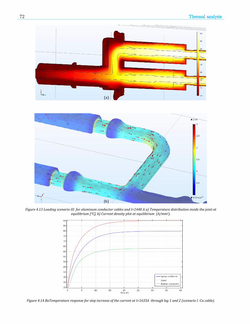
72 Thermal analysis
Figure 4.13 Loading scenario III for aluminum conductor cables and I=1448 A a) Temperature distribution inside the joint at equilibrium [°C], b) Current density plot at equilibrium (A/mm2).
Figure 4.14 BaTemperature response for step increase of the current at I=1635A through leg 1 and 2 (scenario I -Cu cable).
(a)
(b)

73 Thermal analysis
4.6.3. One leg disconnected- Effect on ampacity.
In previous paragraph the unloaded cable was acting as a heat sink. Now we will examine the case when the
unloaded cable does not exist. In the model the cable domains(i.e. conductor, XLPE, sheath, PE) are replaced
with air. The current flowing through path 3 (leg2/leg3) is determined for the temperature to reach 90°C in
steady state. Results can be seen at table 4.6.
Table 4.6: Ampacity of Y-joint with only two cables connected. Tamb=25°C
Loading path
[leg / leg] Continuous current
(θc=90°C) [A]
Al cable conductors leg 2 / leg 3 1350
Cu cable conductors leg 2 / leg 3 1570
The ampacity of the Y-joint reduces by 100 A in Al cables and by 60 A in Cu cables. It obvious that the unloaded
cable has helps in dissipating the generated heat. This means that the size and conductor material of this
cable affects the ampacity of the Y-joint. Removing completely the cable represents the worst case.
Nevertheless, this shall be taken into account by the system’s engineering when cables of small conductor
cross-section are connected at one of the three legs or when blind plugs are installed.
Figure 4.15 Temperature distribution inside the joint at equilibrium. Leg 1 without cable, Leg 2 and 3 with aluminum conductor cables I=1350 A.
4.6.4. Type test heating cycles -Effect of thermal time constant.
In paragraph 4.5 we examined the response of 60 kV cables under heat cycle testing. Similarly to a “dummy
loop” in a type test, we determined the “ON” current value to achieve the required temperatures inside each
cable during a cycle. Now we will apply this heating current as input to the Y-joint model and evaluate the
temperature response of its hottest point. As already mentioned, the conductor temperature inside the Y-
joint should achieve comparable or higher values than that of the cable. In figures 4.15 and 4.16 we see the
temperature response during the 1st cycle, of the cable and the Y-joint, when each of the 4 different cables
listed in table 4.3 are connected.

74 Thermal analysis
Figure 4.16 Y-joint and cable temperature response during 1st heating cycle. a) 1200 mm2 Al cable and Y-joint b) 1600 mm2 Al cable and Y-joint.
Figure 4.17 Y-joint and cable temperature response during 1st heating cycle. a) 1200 mm2 Cu cable and Y-joint b) 1600 mm2 Cu cable and Y-joint.
In figure 4.16a we see that in case we use a 1200 mm2 Al cable for the type test, the conductor temperature
within the joint reaches a maximum of 55°C, which is much below the 90 -100°C range. Thus it cannot be
considered adequate for assessing the thermal design of the Y-joint. Furthermore the difference in thermal
time constants is obvious (τcable<τjoint) is clear since the Y-joint has a slower heating and cooling time
compared to the connected cable.
In figure 4.16b, we see that when a 1600 mm2 Al cable is used, the conductor temperature in the Y-joint
reaches a value of 92°C. Although this is 7°C less than that reached inside the cable, it could be considered
adequate for the purpose of the test. The 16h cooling time is also sufficient for cooling the Y-joint back to
room temperature. This is also proved in figure 4.18 where we can see that after 5 cycles the Y-joint maximum
temperature remains close to 92°C.
In case of Cu cables, similar results are obtained when we use 1200 mm2 Cu cable for the type test (figure
4.17a). In this case though the Y-joint conductor reaches 88°C which is below the desired range of 90-100°C.
When 1600 mm2 Cu cable is used the maximum temperature within the Y-joint reaches 111°C while the
maximum temperature at the cable conductor is 101°C (figure 4.17b). This is much more than the 95-100°C
range, so- this arrangement could prove to be quite stressful for both cable and Y-joint. Nevertheless, such
temperatures have been reached many times during heat cycle type testing. Consequently, the use of 1600
0 2 4 6 8 10 12 14 16 18 20 22 24
25
30
35
40
45
50
55
60
65
70
75
80
85
90
95
100
105
ION
=1220 A, ON-time=8h
time [h]
Tem
pera
ture
[°C
]
Cable conductor
Y-Joint conductor
0 2 4 6 8 10 12 14 16 18 20 22 24
25
30
35
40
45
50
55
60
65
70
75
80
85
90
95
100
105
ION
=1515 A, ON-time=8h
time [h]
Tem
pera
ture
[°C
]
Cable conductor
Y-Joint conductor
0 2 4 6 8 10 12 14 16 18 20 22 2420
25
30
35
40
45
50
55
60
65
70
75
80
85
90
95
100
105
110
115
ION
=1725A, ON-time=8h
time [h]
Tem
pera
ture
[°C
]
Cable conductor
Y-Joint conductor
0 2 4 6 8 10 12 14 16 18 20 22 2420
25
30
35
40
45
50
55
60
65
70
75
80
85
90
95
100
105
110
115
ION
=1980A, ON-time=8h
time [h]
Tem
pera
ture
[°C
]
Cable conductor
Y-Joint conductor
(a) (b)
(a) (b)

75 Thermal analysis
mm2 will result to a firm and unquestionable thermal assessment of the Y-joint. It is up to the design team
and testing team to evaluate the advantages and risks by the use of such cable in the type test loop. In figure
4.19, we see the response of this arrangement during 5 cycles. The cooling time is sufficient and the max
temperatures remain at 110°C.
Figure 4.18 Y-joint and cable temperature response during 5 heating cycles.1600 mm2 Al cable and Y-joint.
Figure 4.19 Y-joint and cable temperature response during 5 heating cycles. 1600 mm2 Cu cable and Y-joint.
0 6 12 18 24 30 36 42 48 54 60 66 72 78 84 90 96 102 108 114 120
25
30
35
40
45
50
55
60
65
70
75
80
85
90
95
100
105
ION
=1515 A, ON-time=8h
time [h]
Tem
pera
ture
[°C
]
Cable conductor Y-Joint conductor
0 6 12 18 24 30 36 42 48 54 60 66 72 78 84 90 96 102 108 114 12020
25
30
35
40
45
50
55
60
65
70
75
80
85
90
95
100
105
110
115
ION
=1980 A, ON-time=8h
time [h]
Tem
pera
ture
[°C
]
Cable conductor Y-Joint conductor
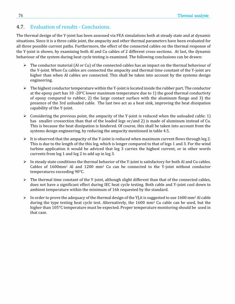
76 Thermal analysis
4.7. Evaluation of results - Conclusions.
The thermal design of the Y-joint has been assessed via FEA simulations both at steady state and at dynamic
situations. Since it is a three cable joint, the ampacity and other thermal parameters have been evaluated for
all three possible current paths. Furthermore, the effect of the connected cables on the thermal response of
the Y-joint is shown, by examining both Al and Cu cables of 2 different cross-sections. At last, the dynamic
behaviour of the system during heat cycle testing is examined. The following conclusions can be drawn:
The conductor material (Al or Cu) of the connected cables has an impact on the thermal behaviour of the Y-joint. When Cu cables are connected the ampacity and thermal time constant of the Y-joint are higher than when Al cables are connected. This shall be taken into account by the systems design engineering.
The highest conductor temperature within the Y-joint is located inside the rubber part. The conductor at the epoxy part has 10 -20°C lower maximum temperature due to 1) the good thermal conductivty of epoxy compared to rubber, 2) the large contact surface with the aluminum flange and 3) the presence of the 3rd unloaded cable. The last two act as a heat sink, improving the heat dissipation capability of the Y-joint.
Considering the previous point, the ampacity of the Y-joint is reduced when the unloaded cable: 1) has smaller crossection than that of the loaded legs or/and 2) is made of aluminum instead of Cu. This is because the heat dissipation is hindered. Of course, this shall be taken into account from the systems design engineering, by reducing the ampacity mentioned in table 4.5.
It is observed that the ampacity of the Y-joint is reduced when maximum current flows through leg 2. This is due to the length of the this leg, which is longer compared to that of legs 1 and 3. For the wind turbine application it would be adviced that leg 3 carries the highest current, or in other words currents from leg 1 and leg 2 to add up in leg 3.
In steady state conditions the thermal behavior of the Y-joint is satisfactory for both Al and Cu cables. Cables of 1600mm2 Al and 1200 mm2 Cu can be connected to the Y-joint without conductor temperatures exceeding 90°C.
The thermal time constant of the Y-joint, although slight different than that of the connected cables, does not have a significant effect during IEC heat cycle testing. Both cable and Y-joint cool down to ambient temperature within the minimum of 16h requested by the standard.
In order to prove the adequacy of the thermal design of the YJ,it is suggested to use 1600 mm2 Al cable during the type testing heat cycle test. Alternatively, the 1600 mm2 Cu cable can be used, but the higher than 105°C temperature must be expected. Proper temperature monitoring should be used in that case.

5 5. Mechanical loading
The accessories of a cable system are subject to mechanical loads during their whole life time, starting even from their production phase. Mechanical stresses arise from temperature differences due to the different thermal expansion coefficients of the materials but also from forces exerted by the connected cables due to the current flowing through them. The Y-joint is a special component regarding its geometry and will have different mechanical behavior compared to the common HV accessories with cylindrical geometries, such as joints and cable terminations. For this reason 3D mechanical simulations are necessary to assess the mechanical behavior of the Y-joint and to identify the limits under various loading scenarios.
The focus in this chapter will be on the mechanical stresses developed in the insulator of the Y-joint. Initially a brief theoretical introduction is made into the Von Mises criterion and the thermal expansion. Then origin of the expected mechanical stresses is identified and examined. This refers to the thermomechanical forces acting from the connected cables in normal operation, the electromagnetic forces and conductor temperatures during short circuit. Afterwards, finite element analysis is performed to identify the limits of the design under the aforementioned loading schemes. The stresses during production are also examined in the last part of this chapter.
5.1. Theoretical formulation
Before dealing with structural mechanics it is important to mention a few basic terminology:
Stress: is the ratio F/A of the force F to the cross-section area A upon which it is applied. It is measured in MPa or N/m2 and can be classified in:
a. Tensile stress σ: when the force acts normal to the stressed area and tends to stretch the material.
b. Compressive stress: the force acts normal to the stressed area and tends to compress or shorten the material.
c. Shearing stress τ: the force acts in parallel to the stressed area and tends to shear the material.
Strain ε: refers to the deformation of the solid due to stress, and is defined by the change in some length parameter divided by the original value of the length parameter:
휀 = 𝛥𝑙
𝑙0 (5.1)
Elasticity modulus or Young modulus Ε: it is material property and measures the stiffness of the material or its resistance to deform elastically when uniaxial force is applied. It is defined as the slope of the tensile stress-strain curve in the elastic deformation region:
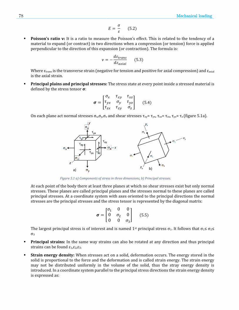
78 Mechanical loading
𝛦 = 𝜎
휀 (5.2)
Poisson’s ratio ν: It is a ratio to measure the Poisson’s effect. This is related to the tendency of a material to expand (or contract) in two directions when a compression (or tension) force is applied perpendicular to the direction of this expansion (or contraction). The formula is:
𝜈 = −𝑑휀𝑡𝑟𝑎𝑛𝑠
𝑑휀𝑎𝑥𝑖𝑎𝑙 (5.3)
Where εtrans is the transverse strain (negative for tension and positive for axial compression) and εaxial is the axial strain.
Principal plains and principal stresses: The stress state at every point inside a stressed material is defined by the stress tensor σ:
𝝈 = [
𝜎𝑥 𝜏𝑥𝑦 𝜏𝑥𝑧
𝜏𝑦𝑥 𝜎𝑦 𝜏𝑦𝑧
𝜏𝑧𝑥 𝜏𝑧𝑦 𝜎𝑧
] (5.4)
On each plane act normal stresses σx,σy,σz and shear stresses τxy= τyx, τxz= τzx, τyz= τz (figure 5.1a).
Figure 5.1 a) Components of stress in three dimensions, b) Principal stresses.
At each point of the body there at least three planes at which no shear stresses exist but only normal stresses. These planes are called principal planes and the stresses normal to these planes are called principal stresses. At a coordinate system with axes oriented to the principal directions the normal stresses are the principal stresses and the stress tensor is represented by the diagonal matrix:
𝝈 = [
𝜎1 0 00 𝜎2 00 0 𝜎3
] (5.5)
The largest principal stress is of interest and is named 1st principal stress σ1. It follows that σ1≤ σ2≤ σ3
Principal strains: In the same way strains can also be rotated at any direction and thus principal strains can be found ε1,ε2,ε3.
Strain energy density: When stresses act on a solid, deformation occurs. The energy stored in the solid is proportional to the force and the deformation and is called strain energy. The strain energy may not be distributed uniformly in the volume of the solid, thus the stray energy density is introduced. In a coordinate system parallel to the principal stress directions the strain energy density is expressed as:
a) b)

79 Mechanical loading
𝑈0 =1
2(𝜎1휀1 + 𝜎2휀2 + 𝜎3휀3) (5.6)
Stresses and strains are related through the linear elastic relations and the energy density can be written in terms of principal stresses:
𝑈0 =1
2𝐸(𝜎1
2 + 𝜎22 + 𝜎3
2 − 2𝜈(𝜎1𝜎2 + 𝜎2𝜎3 + 𝜎1𝜎3)) (5.7)
Yield strength: It is a material property defined as the stress at which a material begins to deform plastically. Prior to the yield point the material will deform elastically and will return to its original shape when the applied stress is removed. Once the yield point is passed, some fraction of the deformation will be permanent and non-reversible. Tensile strength is the ability of the material to withstand elongation (stretching) loads and is expressed in MPa.
Figure 5.2 Stress-strain curve typical for steel.
5.1.1. Von Mises yield criterion.
The strain energy density U0 can be divided into two parts: the dilatational strain energy density Uh which is
responsible for the change in volume, and distortional strain energy density, Ud, that is responsible for change
in shape. Both energy densities can be expressed in terms of principal stresses [37]:
𝑈ℎ =1 − 2𝜈
6𝐸∙ (𝜎1
2 + 𝜎22 + 𝜎3
2 − 2𝜈(𝜎1𝜎2 + 𝜎2𝜎3 + 𝜎1𝜎3)) (5.8)
𝑈𝑑 =1 + 𝜈
3𝐸∙(𝜎1 − 𝜎2)
2 + (𝜎2 − 𝜎3)2 + (𝜎1 − 𝜎3)
2
2 (5.9)
The Von Mises stress is defined as:
𝜎𝑀𝑖𝑠𝑒𝑠 = √(𝜎1 − 𝜎2)
2 + (𝜎2 − 𝜎3)2 + (𝜎1 − 𝜎3)
2
2 (5.10)
1. Ultimate strength 2. Yield strength 3. Rupture 4. Strain hardening region 5. Necking region
A: Apparent stress (F/A0)
B: Actual stress (F/A)

80 Mechanical loading
According to the von Mises’s theory, a ductile solid will yield when Ud reaches a critical value for that material [37]. Thus during a uniaxial tensile test, at the instance of yielding the principal stresses are:
σ1 = σYT (yield stress) and σ2 = σ3 = 0
and the distortion strain energy density is:
𝑈𝑑𝑌 =1 + 𝜈
3𝐸∙ 𝜎𝑌𝑇
2 (5.11)
Thus, UdY is the critical value of the distortional energy density for the material. Then according to von Mises’s failure criterion, the material under multi-axial loading will yield when the distortional energy is equal to or greater than this critical value for the material:
𝑈𝑑 ≥ 𝑈𝑑𝑌 𝑜𝑟 𝜎𝑀𝑖𝑠𝑒𝑠 ≥ 𝜎𝑌𝑇
This means that the material will yield under multi-axial loading when the von Mises stress exceeds the yield stress in a uniaxial tensile test. Since most material properties refer the tensile yield strength, the von Mises criterion will be very useful for engineering purposes, to check if a design can withstand a given load condition. Yield strength values of epoxy and aluminum are found in datasheets and are presented at table 5.1.
Table 5.1: Tensile Yield strength of YJ insulator's materials.
Tensile Yield strength
[MPa]
Epoxy BXH Kufalit 60-80
Cast Aluminium (AlSi7Mg) 220-274
5.1.2. Thermal stress and strain.
When a material is subjected to a change in temperature it tends to change in shape, area, and volume. This is caused by the increase (or decrease) of the kinetic energy of its molecules which leads to an increase (or decrease) of the average separation. This phenomenon is of course material dependent and it is described by the coefficient of thermal expansion α, which measures the fractional change in size per degree change in temperature at a constant pressure. Usually for solids, the coefficient of linear thermal expansion is available, which refers to the change in one dimension:
𝛼𝐿 =1
𝐿∙𝑑𝐿
𝑑𝑇 (5.12)
In terms of strain it can be rewritten as:
휀 = 𝛼𝐿𝛥𝛵 (5.13)
If a body is constrained, then internal stresses can be caused by a temperature change. If the body was free to move and the strain for a specific temperature change is measured, then the stress required to reduce this strain to zero refers to the internal stresses in case the body was constrained. Consequently the internal stresses can be calculated by through the stress/strain relationship characterized by Young’s modulus formula 5.2:
𝜎 = 휀 ∙ 𝛦 → 𝜎 = 𝛦 ∙ 𝛼𝐿 ∙ 𝛥𝛵 (5.14)
This formula will be used to calculate the maximum axial forces exerted on the Y-joint from loaded cables. In table 5.2 we see the value arrange the coefficients α and Ε for epoxy and aluminum.
81 Mechanical loading
Table 5.2. Mechanical and thermomechanical properties of YJ materials.
Coefficient of thermal expansion α
[10-6/ °C]
Elasticity (Young) modulus
[MPa]
Poisson’s ratio
Epoxy BXH Kufalit 30-35 12000-13000 0.3
Cast Aluminium (AlSi7Mg) 21-22 72000-73000 0.33
5.2. Mechanical stresses on Y-joint
As already mentioned, the Y-joint will be continuously subjected to mechanical stresses. These stresses develop during the normal operational life time as well as during the production phase. Furthermore, they can originate from the internal components of the Y-joint insulator (i.e. aluminium conductor, brass inserts) as well as from external components of the Y-joint and more specifically the cables.
5.2.1. Thermomechanical forces from connected cables.
When the current carried by the cable varies in time, a temparure variation inside its components is caused, resulting in thermal expansion or contraction of these components [1]. Especially for cables installed in air, at which temperature variations of 100°C under normal loading condictions may be encountered, these stresses have a considerable influnce on the design of cable installations. Theoretically there are two extremes in installation practise as far as thermomechanical effects are concerned [37] :
a. Where the cable is completely unrestricted and the changes in temperature result in the full extend thermal expansion. In this case no compressive or tensile loads develop.
b. When the cable is fully restrained and no movement of the cable is permitted. In this case the thermal expansion or contraction is fully transferred as uniaxial tensile or compressive forces.
In practice it is not possible to achieve either of the two extreme situations. Nevertheless, in extreme case b, the resulting uniaxial tensile or compressive forces, will act on the cable end and specifically on the accessory it is connected to. Consequently, assuming the worst case scenario at which the cable installation inside the wind turbine is of rigid type, the Y-joint will be subject to axial thrust or pulling forces from the two inter-array cables and from the inner wind turbine cable. These forces will be transferred to the centrepiece of the joint, which is the epoxy insulator. For this reason it is important to analyse the mechanical behaviour of the insulator under uniaxial loading and find any critical areas. Of particular importance is the fixation strength of the M8 metallic inserts that will fix the insulator to the mounting aluminium plate. The latter will be examined in the next paragraph (5.3).
Calculation of thermomechanical forces from single core cable
In practice the conductor and the metallic sheath will be the dominant factors in the thermomechanical effects induced by the cable. A variation of formula 5.14 is used to calculate the force exerted by the conductor and the sheath of a single core cable:
𝐹𝑐𝑜𝑛𝑑−𝑛 = 𝑘1 ∙ 𝑆𝑐𝑜𝑛𝑑 ∙ 𝛦𝑐𝑜𝑛𝑑 ∙ 𝛼𝑐𝑜𝑛𝑑 ∙ (𝑇𝑐𝑜𝑛𝑑 − 𝑇𝑎𝑚𝑏) (5.15)
𝐹𝑠ℎ−𝑛 = 𝑘2 ∙ 𝑆𝑠ℎ ∙ 𝛦𝑠ℎ ∙ 𝛼𝑠ℎ ∙ (𝑇𝑠ℎ − 𝑇𝑎𝑚𝑏) (5.16)
82 Mechanical loading
where Scond and Ssh are the electrical cross-section areas of the conductor and sheath respectively, and k1 , k2 the daily relaxation factors for the conductor and sheath respectively. The relaxation factors are taken empirically from project engineers and usually are in the range of 0.65 and 0.75. The conductor temperature is taken at 90°C which is the maximum allowable temperature on the surface of the conductor. The sheath temperature attains a maximum value at the range of 70°C during maximum load.
Formulas, 5.15 and 5.16 consider only the daily thermal cycle of the cable, since only the difference from temperature difference between no-load and fully load is taken into account. In reality, the installation conditions also have an influence since, the installation temperature will be different from the average ambient temperature. Those forces are calculated in the same way:
𝐹𝑐𝑜𝑛𝑑−𝑖 = 𝑘3 ∙ 𝑆𝑐𝑜𝑛𝑑 ∙ 𝛦𝑐𝑜𝑛𝑑 ∙ 𝛼𝑐𝑜𝑛𝑑 ∙ (𝑇𝑎𝑚𝑏 − 𝑇𝑖𝑛𝑠𝑡𝑎𝑙) (5.17)
𝐹𝑠ℎ−𝑖 = 𝑘4 ∙ 𝑆𝑠ℎ ∙ 𝛦𝑠ℎ ∙ 𝛼𝑠ℎ ∙ (𝑇𝑎𝑚𝑏 − 𝑇𝑖𝑛𝑠𝑡𝑎𝑙) (5.18)
where k3 , k4 the seasonal relaxation factors for the conductor and sheath respectively.
The total thermomechanical force from the connected cable on each of the legs of the Y-joint insulator is:
𝐹𝑡𝑜𝑡 = 𝐹𝑐𝑜𝑛𝑑−𝑛 + 𝐹𝑠ℎ−𝑛 + 𝐹𝑐𝑜𝑛𝑑−𝑖 + 𝐹𝑠ℎ−𝑖 (5.19)
At table 5.3 the total force is calculated for cables with copper conductor and aluminium sheath, assuming Tamb=25°C and Tinst=20°C. We can see that for 1600 mm2 cable conductor, the force on the insulator could reach 52.2 kN. This force will can increase even more when the ambient and installation temperatures are lower. Similar tables for various conductor and sheath materials can be found in appendix B.
So far the material is assumed to be in the elastic region and the force to be proportional to the temperature rise. In reality, when high temperatures are reached the metallic parts of the cable enter the plastic region, resulting in permanent deformation. Due to this phenomenon, when the cable is allowed to cool to its initial temperature, tensile forces develop at the cable end (especially for fully restrained cables). After repeated heat cycles, the compressive and tensile forces reach the same magnitude during the respective heating and cooling periods (figure 5.3b) [37].
Figure 5.3 a) Force versus temperature characteristic for a restrained single core cable with Milliken conductor, b) Tensile and compressive forces generated in a single-core cable during loading cycles [37].
a) b)

83 Mechanical loading
Table 5.3: Tensile/Compressive forces in Nt from cables with copper conductor and aluminum sheath.
Conductor area
[mm2]
240 300 400 500 630 800 1000 1200 1600
Metallic sheath
area
[mm2]
28 8310 10078 13026 15974 19806 24817 30713 36608 48400
50 9280 11048 13996 16944 20776 25787 31683 37579 49370
61 9765 11534 14481 17429 21261 26273 32168 38064 49855
70 10162 11930 14878 17826 21658 26669 32565 38461 50252
95 11264 13033 15981 18929 22761 27772 33668 39563 51354
115 12146 13915 16863 19811 23643 28654 34550 40445 52236
Cantilever forces
In an ideal cable installation the total thermomechanical force would be applied along the main axis of the cable and the YJ insulator’s leg. Of course some misalignment is always present, meaning that the force would be applied in an angle to the main axis, and the leg of the insulator would be subjected into cantilever force. Considering a maximum angle of 5 degrees the cantilever force would be:
𝐹𝑐𝑎𝑛𝑡 = 𝐹𝑡𝑜𝑡 ∙ sin(5°) (5.20)
For a total force of 50 kN the cantilever force would be 4.3 kN.
5.2.2. Stresses due to short circuit currents.
The short circuit in an electrical system represents a severe situation which brings the electrical equipment to its limits. Especially for high voltage equipment, the grid they are connected to is much stronger compared to MV grid, resulting in higher short circuit currents. Although such currents last only hunderds of miliseconds, cables and their accessories are subject to sudden conductor temperature rises and also high electromechanical forces.
5.2.2.1. Magnetic forces due to short circuit currents.
When two current carrying conductors have their axis in parallel, they are subject to radial magnetic forces which depend on their length, the current and the distance between their axis. Assuming the current is the identical for both conductors the radial force is:
𝐹𝑀 = 𝐵 ∙ 𝐼 ∙ 𝐿 →
𝐹𝑀 = 𝜇0 ∙𝐼2
2𝜋𝑠∙ L (5.21)
where μ0=4π·10-7 H·m-1
s is the distance between the conductors’ axis [m]
L is the length of the conductor [m]
Figure 5.4 Most severe short circuit current path inside YJ.

84 Mechanical loading
I is the current [A]
The most critical situation for a Y- joint, is when the short circuit current is flowing as in figure 5.4. The distance between the two axis is s=220 mm. The length of the conductors will be taken 1m, which usually corresponds to the maximum distance of the cable cleats from the joint. The magnetic force due to short circuit transfers a cantilever force applied on the legs of the epoxy insulator. The maximum force will develop when the short circuit current reaches its maximum value during the dynamic state. The theoretical value of
this is 1.8√2 the static short circuit value (figure 5.5).
The tolerable cantilever force for the epoxy will be calculated via the finite element analysis in the following paragraph. By inverting formula 5.21, the maximum tolerable static short circuit current can be found:
𝐼𝑠𝑐_𝑡𝑜𝑙 =1
1.8√2∙ √
𝐹𝑡𝑜𝑙 ∙ 2𝜋 ∙ 𝑠
𝜇0 ∙ L (5.22)
5.2.2.2. Thermal stress due to short circuit current.
The short circuit current will cause a temperature rise in the aluminium conductor of the YJ insulator. This
temperature rise is assumed adiabatic during the short duration of the fault, meaning that the energy of the
short circuit contributes to the temperature rise of only the conductor. As a result, the conductor will expand
very fast causing internal stresses at both the aluminium and the epoxy.
In order to calculate the developing stresses, it is important to know the temperature of the conductor at the
time the short circuit is cleared. This can be calculated in two ways:
1. Assuming the resistance of the conductor constant and independent of the conductor temperature T. This method is used for the short circuit current capacity of cables.
2. The temperature coefficient α is taken into account so that conductor’s resistance increases with temperature resulting in higher conductor temperatures.
In both methods the starting conductor temperature is
assumed to be at 90°C, corresponding to the maximum
allowed current load.
Method 1
The total energy Q required to change the temperature of a mass m with heat capacity Cp by Δθ degrees is:
𝑄 = 𝐶𝑝 ∙ 𝑚 ∙ 𝛥𝜃 (5.23)
This energy is provided by the short circuit current Isc during tsc seconds:
𝑄 = 𝐼𝑠𝑐2 ∙ 𝑅 ∙ 𝑡𝑠𝑐 (5.24)
It s known that:
𝑅 = 𝜌𝑐
𝐿
𝐴 𝑎𝑛𝑑 𝑚 = 𝑑 ∙ 𝐴 ∙ 𝐿
Figure 5.5 Short circuit current waveform.
Theoretical maximum
Static maximum

85 Mechanical loading
where A: conductor cross section, L: conductor’s length, ρc: resistivity of the conductor and d: density.
From the aforementioned formulas we get:
𝛥𝜃 =𝐼𝑠𝑐
2 ∙ 𝜌𝑐 ∙ 𝑡𝑠𝑐𝛢2 ∙ 𝐶𝑝 ∙ 𝑑
(5.26)
The resistivity is constant and its value is taken at 90°C including the skin and proximity effect factors. According to formula 4.9 from the previous chapter:
𝜌𝑐(𝜃𝑐) = 𝜌20
[1 + 𝛼20(𝜃𝑐 − 20)] (1 + 𝑦𝑠+ 𝑦
𝑝)
𝜌𝑐(90) = 3.938 ∙ 10−8 𝛺 ∙ 𝑚
The conductor temperature will be :
𝜃𝑐(𝑡𝑠𝑐) = 90 +𝐼𝑠𝑐
2 ∙ 𝜌𝑐
𝛢2 ∙ 𝐶𝑝 ∙ 𝑑∙ 𝑡𝑠𝑐 (5.27)
Method 2
From the definition of the heat capacity we get:
𝑤 = 𝑚 ∙ 𝐶𝑝
𝑑𝜃
𝑑𝑡 (5.28)
The heat rate w is provided by the power loss due to the short circuit current Isc:
𝑤 = 𝐼𝑠𝑐2 ∙ 𝑅(𝜃) (5.29)
From equations 4.2 and 4.3 the resistance as function of the the temperature is:
𝑅(𝜃𝑐) = 𝐿 ∙1.02 ∙ 106
𝐴∙ 𝜌20[1 + 𝛼20(𝜃𝑐 − 20)] ∙ (1 + 𝑦𝑠 + 𝑦𝑝) (5.30)
By combining 5.24 and 5.23 ( and with m=d·A·L), we get:
𝑑 ∙ 𝐴 ∙ 𝐿 ∙ 𝐶𝑝
𝑑𝜃𝑐
𝑑𝑡= 𝐼𝑠𝑐
2 ∙1.02 ∗ 106
𝐴∙ 𝜌
20[1 + 𝛼20(𝜃𝑐 − 20)] ∙ (1 + 𝑦
𝑠+ 𝑦
𝑝)
Rearranging this equation gives:
𝑑𝜃𝑐
[1 + 𝛼20(𝜃𝑐 − 20)]= 𝐼𝑠𝑐
2 ∙1.02 ∙ 106
𝐶𝑝 ∙ 𝑑 ∙ 𝐴2 ∙ 𝜌20
∙ (1 + 𝑦𝑠+ 𝑦
𝑝) 𝑑𝑡
or
𝑑𝜃𝑐
[1 + 𝛼20(𝜃𝑐 − 20)]= 𝐼𝑠𝑐
2𝑏 𝑑𝑡 (5.31)
where:
𝑏 =1.02 ∙ 106
𝐶𝑝 ∙ 𝑑 ∙ 𝐴2 ∙ 𝜌20
∙ (1 + 𝑦𝑠+ 𝑦
𝑝) (5.32)

86 Mechanical loading
Integrating equation 5.31 we get:
∫𝑑𝛩𝑐
[1 + 𝛼20(𝛩𝑐 − 20)]
𝜃𝑐
𝜃𝑖𝑛
= ∫𝐼𝑠𝑐2𝑏 𝑑𝜏
𝑡
0
→
[1
𝛼20
𝑙𝑛(1 + 𝛼20(𝛩𝑐 − 20))]𝜃𝑖𝑛
𝜃𝑐
= [𝐼𝑠𝑐2𝑏𝜏]
0
𝑡→
𝑙𝑛 (1 + 𝛼20(𝜃𝑐 − 20)
1 + 𝛼20(𝜃𝑖𝑛 − 20)) = 𝐼𝑠𝑐
2𝛼20𝑏 ∙ 𝑡 (5.33)
The conductor temperature as function of time for a given short circuit current Isc is:
𝜃𝑐(𝑡𝑠𝑐) = 20 +1
𝛼20(𝑒𝐼𝑠𝑐
2𝛼20𝑏∙𝑡𝑠𝑐 (1 + 𝛼20(𝜃𝑖𝑛 − 20)) − 1) (5.34)
At figure 5.6 we see the conductor temperature of the YJ as function of the short circuit time. The two methods are compared for short circuit currents of 50 kA (figure 5.6a) and 100 kA (figure 5.6b). It is obvious that the effect on the resistivity of the temperature constant α, is greater as the short circuit current increases. A high short circuit current results in higher losses and thus in higher temperature increase. Since method 2 represents more the real situation it will be used further in chapter 5.4.
Figure 5.6 Temperature versus short circuit duration for a) Isc=50 kA and b) Isc=100 kA
As a result of the temperature rise, the conductor will expand causing internal stresses at both aluminum and epoxy. The governing formula is:
𝜎 = 𝐸 ∙ 𝑎 ∙ ( 𝜃𝑐(𝑡) − 90) (5.35)
Due to the complex geometry of the insulator, it is appropriate to use FEM analysis to find the temperature at which the thermal expansion would stress materials of the insulator to their limits:
𝜎𝐴𝑙(𝜃𝑐) ≤ 𝜎𝛶−𝐴𝑙 𝑜𝑟 𝜎𝑒𝑝(𝜃𝑐) ≤ 𝜎𝛶−𝑒𝑝 (5.36)
90
110
130
150
170
190
0 0 , 5 1 1 , 5 2 2 , 5 3
θc [°
C]
Short circuit duration [s]
Method 1 Method 2
90
190
290
390
490
590
690
0 0 , 5 1 1 , 5 2 2 , 5 3
θc
[C]
Short circuit duration [s]
Method 1 Method 2
a) b)

87 Mechanical loading
5.2.3. Thermal stress during production.
Following the curing process of the epoxy during production, the insulator is left to cool down from a temperature of 70-80°C down to room temperature. Due to the different thermal expansion coefficients of epoxy and aluminium the epoxy will shrink more than the aluminum conductor resulting in stresses which may lead to delamination or cracking.
Using FEM we can investigate the stress development after the cooling period. The simulation will be performed in steady state.
5.3. Yield strength of fixation components
5.3.1. Brass threaded inserts - Adhesion with epoxy.
In order to fix the insulator on the aluminium base plate, four brass inserts with M8 thread are embedded around each cone at a diameter of 185 mm, as shown in figure 5.7. These inserts must withstand forces that tend to separate the insulator from the plate, such as thrust forces, resulting from the connected cables due to thermomechanical loading. During such loading, the epoxy around the inserts is stressed as well as the adhesion of the brass-epoxy interface. When one of the two limits are reached the insert is pulled out of the epoxy.
The adhesion strength can be defined as follows:
𝑇𝑌 =𝐹𝑝𝑢𝑙𝑙
𝐴 [
𝑁
𝑚𝑚2 𝑜𝑟 𝑀𝑃𝑎] (5.37)
where Fpull the pull out force along the axis of the insert and A is the contact surface with the epoxy. For an M8 insert the contact surface is A=961 mm2.
Figure 5.7 Insulator with embedded M8 threaded brass inserts.
While the yield strength of epoxy is known, the yield strength of the brass-epoxy interface is not specifically given by the manufacturer. Nevertheless, we can calculate the yield strength from actual pressure burst tests that have been performed on existing epoxy products. In such tests, the inserts are used to fix a metallic plate on which pressure is applied. At the end of the test the pressure force is such that the inserts are pulled out from the epoxy together with the screws that hold the plate.

88 Mechanical loading
More specifically, data from a pressure burst test performed on a 245 kV dry type termination with M10 brass inserts, showed that the pull-out force per insert was Fpull= 17.67 kN. The contact surface A of the M10 insert is A=1228 mm2. This results in an epoxy-brass adhesion strength of:
𝑇𝑌 =17,67𝑘𝑁
1228𝑚𝑚2= 14,39 𝑀𝑃𝑎
It is known now that traction stress higher than 12.79 Mpa will result in yielding of the epoxy-brass interface.
For an M8 this translates into a pull out force of:
𝐹𝑌𝑀8 = 14.39𝑀𝑝𝑎 ∙ 961𝑚𝑚2 = 13.83 𝑘𝑁
5.3.2. Yield strength of M8 bolts.
The plate and epoxy are held together via eight M8 hexagonal socket bolts as shown in figure 5.8. These bolts are made out of high strength stainless steel (RVS-70). These bolts must withstand thrust forces as previously explained for the epoxy-brass interface. The tensile yield strength of each bolt is given by the manufacturer and is FYB=16.4 kN.
Taking into account that these bolts are pre-stressed after being fastened on the inserts, the allowable tensile force is lower than FYB:
𝐹𝐵𝑟 = 𝐹𝑌𝐵 − 𝐹𝐹𝑆 = 𝐹𝑌𝐵 − 𝛼𝐹𝑌𝐵 = 𝐹𝑌𝐵(1 − 𝑎)
Where FFS is the fastening force and α is the fastening force ratio. We can see that the lower the ratio α the higher the allowable force on the bolt. Nevertheless, it is not recommended that takes very low values. For our application it is chosen that α=0.45, which means that the allowable force for the bolt is:
𝐹𝐵𝑟 = 9.02 𝑘𝑁
This allowable force is much lower than the limit set by the pull out strength of the brass insert. In other words, the limiting factor in the fixation scheme are the bolts since those will yield first.
Dividing this limit with the surface area of the M8 insert we get:
𝑇𝐵𝑟 =9020𝑁
961𝑚𝑚2= 9.39 𝑀𝑃𝑎
Since this force is transferred directly to the interface of the brass insert with the epoxy, it will be used as a maximum allowable stress, referring to the allowable force on the M8 bolt.
5.4. Withstand capability of Y-joint under uniaxial loads.
In this paragraph, a mechanical FEM analysis will be performed on the insulator of the Y-joint, using the solid mechanics module of COMSOL Multiphysics in a stationary study. Initially the 3D geometry is built with the aid of a commercial CAD software due to the design’s complexity. Then, the geometry is imported in the FEM software. The physics are defined, the boundary conditions are set and the mesh is created. After completing those steps the model is processed by the software. The obtained data is post-processed to derive the wanted
-z
Figure 5.8 M8 RVS-70 hex. socket bolt.

89 Mechanical loading
values and plots of the Von Mises stresses and displacement and extract the traction force exerted on the fixation inserts.
The suggested loading scenarios are summarized in the table 5.4. The notation for the force’s direction is shown at figure 5.8. The Y-joint is assesed for tensile-compressive forces (scenario 1-11) as well as for cantilever forces (scenario 12-19). According to this table the loading scenarios are focused on each leg alone and on combination of two legs. Each insulator’s leg is simulated for both thrust and pulling forces (T&P), and for cantilever forces along each of the basic directions (W&N).
These scenarios are representative of situations encountered at the actual Y-joint assembly. For example, scenario 7 represents a situation at which the Y-joint is experiencing large thrust forces at leg 2 and 3 from the connected cables. Since leg 2 and 3 are connected with the interarray cables, which are of much larger cross-section than the inner wind-turbine cable, the forces from those cables will be the most critical. Scenario 8 to 10, examine the stresses mainly in the vertical part aluminum insert since the forces are acting on the same axis. Scenario 18 and 19, are representative of cantilever forces due to short circuit currents.
Table 5.4: Direction of forces per loading scenario.
Leg 1 Leg 2 Leg 3 Leg 1 Leg 2 Leg 3
Tensile- compressive
load
Scenario 1 -z - -
Cantilever load
Scenario 12 x - -
Scenario 2 - -z - Scenario 13 y - -
Scenario 3 - - -z Scenario 14 - x -
Scenario 4 z - - Scenario 15 - y -
Scenario 5 - z - Scenario 16 - - x
Scenario 6 - - z Scenario 17 - - y
Scenario 7 - -z -z Scenario 18 - -x x
Scenario 8 -z - -z Scenario 19 - x -x
Scenario 9 z - z Scenario 20 - -y y
Scenario 10 z - -z
Scenario 11 -z -z -
Figure 5.9 Direction notation of applied forces.
z
-z
-y
y
x -x
90 Mechanical loading
5.4.1. Building the 3D geometry.
For the solid mechanics simulation, a 3D model of the insulator is created. The model should include details of the conductor and the M8 inserts. In order to reduce the complexity of the model and avoid unnecessary increase of the mesh elements, which would increase the computational time, the following simplifications are made:
g. The pin holes of the Click-Fit ends of the aluminum conductor are not included in the model. Details of this are out of the scope of this report since they have been repeatedly tested in the past and have been in operation inside terminations and joints for many years. This simplification will allow mesh completion and reduce a lot the computational time.
h. The simulation domain will not include the inner body of the M8 inserts. The load on each insert will be calculated at its interface with the epoxy.
The three dimensional geometry imported at COMSOL Multiphysics is shown at figure 5.10a.
Figure 5.10 a) Imported 3D geometry of Y-joint insulator and b) Generated mesh with tetrahedral elements.
5.4.2. Boundary conditions and domain properties.
After the geometry is imported, the simulated domains must be assigned with material properties. For the solid mechanics module the material properties to be defined are: the elasticity modulus, the Poisson’s ratio and the density. These are presented at table 5.5 and are taken from material specifications provided by Prysmian’s suppliers.
Table 5.5: Material properties for mechanical simulation.
Aluminum Epoxy
Elasticity (Young) modulus [GPa] 73 12
Poisson’s ratio 0.33 0.3
Density [kg/m3] 2697 1850
a) b)

91 Mechanical loading
Before the simulation the proper boundary conditions must be set:
Fixed constraint surface boundary: this adds a condition that makes the geometric entity fixed. This means for the selected boundary the displacement is zero at all directions. For all simulations this constraint is applied at the boundary of the M8 inserts as shown in figure 5.11a.
Surface boundary load: This adds a condition for the value and direction of the applied force. An example is given at firure 5.11b for the boundary at which compressive/pulling force is applied and at figure 5.11c for the boundary at which cantilever force is applied. It should be noted that in reality those forces are applied on different surfaces that are not included in the geometry for simplicity reasons as explained before. These boundaries serve as the force input in our model and stresses resulting inside the click-fit end will not be evaluated.
Figure 5.11 a) Fixed constraint boundaries, b) loading surface for compressive/tensile forces at leg 2 and c) loading surface for cantilever forces at leg 2.
5.4.3. Mesh generation.
All simulation domains are meshed with free tetrahedral elements. In general, a fine mesh is desired in order to obtain accurate results and good resolution at the areas of interest. This particularly important at the vicinity of the M8 inserts where high stresses are expected. The mesh is optimized and the restrictions given are:
Minimum element size: 4 mm Maximum element size: 80 mm Maximum element growth rate: 2 Curvature factor: 0.35 Number of elements: 97366
A preview of the mesh is shown at figure 5.10b. The mesh quality is assesed by the minimum element quality,
which should be greater than 0.1. The generated mesh has a minimum element quality of 0.53, which is more
than required
a) b) c)

92 Mechanical loading
5.4.4. Results.
All the loading scenarios that have been presented at table 5.4 are simulated. The developed stresses are
firstly evaluated using the von Mises criterion, at which the stress values are compared with the tensile yield
strength of the material (epoxy or aluminium) presented at table 5.1. Values greater than the limit pose risk
for the component. Secondly, the stress at the brass/epoxy interface of each M8 insert is found from the value
of the traction stress (z-component). This value is compared with the limit found at paragraph 5.3.2. If greater
than 9.39 MPa the M8 bolt that is fixed at this insert will yield. Therefore the maximum force per scenario is
determined by the force at which one of aforementioned limits (von Mises or traction stress) is reached.
The evaluation process will be demonstrated for two of the loading scenarios at table 5.4. The maximum force
per scenario and the cause of the limit are summarized at table 5.8.
Scenario 7- Compressive (thrust) forces at leg 2 and leg 3
As already mentioned this scenario represents a loading case at which thrust forces are exerted on legs 2 and
3 of the insulator resulting from thermal expansion of the inter-array cables. Due to the large difference in
conductor cross-section, between the inner turbine and inter-array cables, the force at leg 1 is assumed zero.
In this simulation 34.5 kN is applied at leg 2 and 3 at -z direction.
The results can be seen at the following pages. Figure 5.12a shows a 3D plot of the total displacement
including a visualization of the deformation with a factor of 300. We can see that both cones are forced
towards the -z direction with the inserts trying to oppose this change. This results in stresses around those
inserts which is obvious at figure 5.12b. In order to find the design’s limitation we examine the two criteria.
Von Mises Stress criterion
From figure 5.13 we see that the von Mises plot of the aluminium conductor does not give stresses that are
critical for the aluminium. Most of the stresses are located close to the connector where the force is applied.
The average value at this area is around 20-25 MPa with a peak of 29.7 MPa, much lower than the critical
region of 220-274 MPa.
The epoxy is also not critically stressed as can be seen at figures 5.14 and 5.15. The conical part experiences
stresses with a peak of 12.5 MPa that is concentrated at the top of the cone at the interface with aluminium.
The highest stresses though are located at the vicinity of the fixation inserts (figure 5.15), which is expectable
since these are fixing the whole component. Peak stresses of 36 MPa can be found at the surface of those
inserts. Nevertheless all the values stay below the critical range for epoxy which is 60-80 MPa.
Epoxy-brass interfacial stress criterion
The stress along the interface of each insert is evaluated via the z-component of the traction parameter
(solid.Taz). This value is expressed in MPa and is compared with the limit of 9.39 MPa which corresponds to
the yielding of the M8 stainless steel bolt. A number is given at each insert, to enable its identification (figure
5.16). Results are given in the table below. The force on each insert can be found by multiplying the stress
with the surface area 961 mm2.

93 Mechanical loading
Table 5.6: Epoxy/brass interfacial stress per insert
Insert 1 Insert 2 Insert 3 Insert 4 Insert 5 Insert 6 Insert 7 Insert 8
Traction [MPa] 8,43 8,47 9,17 9,38 8,99 9,05 8,52 8,51
Force [N] 8110 8148 8817 9024 8647 8702 8200 8189
We can see that the interfacial stress is not uniformly distributed at all 8 inserts. The inserts at the middle of
the insulator are stressed more than the outer inserts. More specifically, insert number 4 is the most stressed
insert (~14% more than insert 1) and this determines the limitation of the design. Forces exceeding the 34.5
kN per leg will result in yielding of the bolt connected at insert number 4. Adding the forces results in 67.8
kN which is close to the 69 kN applied on the Y-joint. The difference can be attributed to the low resolution
of the mesh at this area.
Figure 5.12 Compressive load 34.5 kN, a) displacement 3D plot [mm], b) Von Mises plot [MPa].Deformation factor 300.
a) b)

94 Mechanical loading
Figure 5.13 Compressive load 34.5 kN, Von Mises stresses at aluminum conductor [MPa] a) 3D view and b) across cut plane 1.
a)
b)
b)

95 Mechanical loading
Figure 5.14 Compressive load 34.5 kN, a) Von Mises stresses in epoxy across cut plane 1[MPa], b) cut plane 1.
Figure 5.15 Compressive load 34.5 kN, a) Von Mises stresses in epoxy at the inserts’ surface [MPa], b) Von Mises stress in epoxy across cut plane 2[MPa], c) Cut plane 2.
a)
b) c)
a) b)

96 Mechanical loading
Figure 5.16 Identification of M8 inserts.
Scenario 18- Cantilever forces at leg 2 and leg 3
This scenario represents a loading case at which cantilever forces are exerted on legs 2 and 3 from the cables
due to the circulation of short circuit. The current through each leg has opposite sign meaning that attraction
forces develop. If the location of the fault is at the inner cabling of the wind turbine then the short circuit
current through legs 2 and 3 would be of the same sign. In this case the repelling forces will develop. In this
simulation 22 kN is applied at leg 2 and 3 at -z direction.
The results can be seen at the following page. Figure 5.17a shows a 3D plot of the total displacement including
a visualization of the deformation with a factor of 80. We can see that both cones are forced towards each
other. Stresses are developed at the base of the cone as well as at the top close to the interface with the
aluminium conductor. The inserts are also stressed with those in the middle (3 to 6) experiencing pull-out
forces and those at the edge push-in forces. The pull-out forces are of interest in this case. Again, in order to
find the design’s limitation we examine the two criteria.
Von Mises Stress criterion
According to figure 5.18 the stresses at the aluminum conductor are higher compared to the previous
scenario. Nevertheless, they are almost half of the allowable stress. The peak stress is located at the neck of
the thick side of the conductor and is 139 MPa, much lower than the critical region of 220-274 MPa.
The epoxy is also not critically stressed as can be seen at figures 5.19. The conical part experiences stresses
with a peak of 47.8 MPa that is concentrated at the top of the cone at the interface with aluminium. The
highest stresses though are located at the vicinity of the fixation inserts (figure 5.20). Peak stresses of 56 MPa
can be found at the surface of those inserts. Nevertheless all the values stay below the critical range for epoxy
which is 60-80 MPa.
Epoxy-brass interfacial stress criterion
The stress along the interface of each insert is evaluated via the z-component of the traction parameter
(solid.Taz). This value is expressed in MPa and is compared with the limit of 9.39 MPa which corresponds to
the yielding of the M8 stainless steel bolt. Results are given in the table below.
1
2 3
4 5
6 7
8

97 Mechanical loading
Table 5.7: Epoxy/brass interfacial stress per insert- cantilever load.
Insert 1 Insert 2 Insert 3 Insert 4 Insert 5 Insert 6 Insert 7 Insert 8
Traction [MPa] -9.41 -9.58 9.6 9.58 9.33 9.32 -9.35 -9.46
The interfacial stress is uniformly distributed at the 8 inserts. The negative sign indicates pushing force. The
interfacial stress at the middle inserts is of interest since they are experiencing pull-out forces. The value is
higher than the allowable, thus cantilever force higher than 22 kN should be avoided.
From equation 5.22 the tolerable static short circuit current giving such cantilever force is:
𝐼𝑠𝑐_𝑡𝑜𝑙 =1
1.8√2∙ √
𝐹𝑡𝑜𝑙 ∙ 2𝜋 ∙ 𝑠
𝜇0 ∙ L= 86.4 kA
where s=220 mm and L=500 mm. For higher short-circuit currents the clamping distance should be
decreased to less than 500 mm.
Figure 5.17 Cantilever loading 22 kN, a) displacement 3D plot [mm], b) Von Mises plot [MPa].Deformation factor 80.
a) b)

98 Mechanical loading
Figure 5.18 Cantilever loading 22 kN, Von Mises stresses at aluminum conductor [MPa] a) 3D view and b) across cut plane 1.
a)
b)
99 Mechanical loading
Figure 5.19 Cantilever loading 22 kN, a) Von Mises stresses in epoxy across cut plane 1[MPa], b) cut plane 1.
Figure 5.20 Cantilever loading 22 kN, a) Von Mises stresses in epoxy at the inserts’ surface [MPa], b) Von Mises stress in epoxy across cut plane 2[MPa], c) Cut plane 2.
a) b)
b) c)
a)
100 Mechanical loading
Table 5.8: Design limits per loading scenario.
Leg 1 Leg 2 Leg 3 Maximum force
[kN] Limitation
Tensile- compressive
load
Scenario 1 -z - - F1=34.5 Bolts Nr.7&8
Scenario 2 - -z - F2=34.5 Bolts Nr.1&2
Scenario 3 - - -z F3=34.5 Bolts Nr.7&8
Scenario 4 z - - F1=54.8 Epoxy around inserts
Scenario 5 - z - F2=54.8 Epoxy around inserts
Scenario 6 - - z F3=54.8 Epoxy around inserts
Scenario 7 - -z -z F2=F3=69 Bolt Nr.4
Scenario 8 -z - -z F1+F3=69 Bolts Nr.7&8
Scenario 9 z - z F1+F3= 54.8 Epoxy around inserts
Scenario 10 z - -z F3 - F1=69 Bolt Nr.4
Scenario 11 -z -z - F1+F2=69 Bolt Nr.4
Cantilever load
Scenario 12 x - - F2=24 Epoxy around inserts
Scenario 13 y - - F2=12 Bolt Nr.7
Scenario 14 - x - F2=24 Epoxy around inserts
Scenario 15 - y - F2=19 Bolt Nr.8
Scenario 16 - - x F2=24 Epoxy around inserts
Scenario 17 - - y F3=18 Bolt Nr.1
Scenario 18 - -x x F2=F3=22 Bolt Nr.3
Scenario 19 - x -x F2=F3=22 Bolt Nr.2
Scenario 20 - -y y F2=F3=19 Bolts Nr.1&7
The withstand capability of the Y-joint under tensile-compressive forces is limited at 34.5kN (at -z direction) for leg 2 and for the combination of leg 1 and leg 3. The latter means that total force from both legs at the -z direction must not exceed 34.5kN. For instance, it is possible that there is a simultaneous development of compression forces at leg 3 (-z direction) and tension forces at leg 1(-z direction). Consequently, the sum of the maximum thermomechanical force from the cable connected at leg 1 and the maximum thermomechanical force from the cable connected at leg 3 must not exceed 34.5 kN at the -z direction.
For the system’s design engineering it is important to consider the following:
Maximum Thermomechanical force of cable at leg 2: 𝐹𝑐𝑎𝑏𝑙𝑒−𝑙𝑒𝑔2 ≤ 34.5 [𝑘𝑁]
Maximum Thermomechanical force of cable at leg 1: 𝐹𝑐𝑎𝑏𝑙𝑒−𝑙𝑒𝑔1 ≤ 34.5 − 𝐹𝑐𝑎𝑏𝑙𝑒−𝑙𝑒𝑔3 [𝑘𝑁]
Maximum Thermomechanical force of cable at leg 3: 𝐹𝑐𝑎𝑏𝑙𝑒−𝑙𝑒𝑔3 ≤ 34.5 − 𝐹𝑐𝑎𝑏𝑙𝑒−𝑙𝑒𝑔1 [𝑘𝑁]
Example from table 5.3
Taking into account the aforementioned limits, leg 2 can be connected with a 1000mm2 Cu-95mm2Al cable as according to table 5.3, the maximum forces are 33.67 kN ≤ 34.5 kN.

101 Mechanical loading
Assuming that leg 1 is connected with a cable of much smaller cross-section than that of leg 3 (which is the case for the Y-joint at the wind farm), the smallest cable of table 5.3 is the 240m2 Cu-28mm2Al cable. This means that the thermomechanical force on leg 3 should be less than:
𝐹𝑐𝑎𝑏𝑙𝑒−𝑙𝑒𝑔3 ≤ 34.5 − 𝐹𝑐𝑎𝑏𝑙𝑒−𝑙𝑒𝑔1 = 34.5 − 8.31 = 26.19 𝑘𝑁
Thus the largest cable that can be connected at leg 3 is the 800mm2 Cu-50mm2Al cable.
Of course, this calculation refers to a rigid installation of the cable system. A more flexible installation would result in less thermomechanical forces acting on the Y-joint. In other words, cables of larger conductor cross-section could be connected to Y-joint if flexible installation of the cable system is foreseen.
5.5. Thermal stress during a short circuit.
As already explained, the circulation of short circuit current through the Y-joint, will result in a fast increase
of the conductor’s temperature and thus a fast thermal expansion of the material, giving rise to stresses in
both epoxy and aluminium. Since the expansion is mainly dependent on the initial and final temperature of
the conductor, we need to find the final temperature at which the expansion of the aluminium conductor is
such that the resulting stresses in either the epoxy or the aluminium, become critical according to table 5.1.
Knowing the critical temperature, the allowable short circuit current can be calculated (for certain duration)
using the formulas from paragraph 5.2.2 for adiabatic temperature rise. A plot is then made of the allowable
short circuit current as function of the short circuit duration can be made.
In this paragraph, a thermal expansion FEM analysis will be performed on the insulator of the Y-joint, using
the solid mechanics and heat transfer module of COMSOL Multiphysics in a stationary study. Both modules
are coupled together using the thermal expansion sub-node. This sub-node adds a thermal strain caused by
changes in temperature. The steps are similar to the mechanical simulation performed earlier. Initially the
3D geometry is built with the aid of a commercial CAD software. Then, the geometry is imported in the FEM
software. The physics are defined, the boundary conditions and domain properties are set and the mesh is
created. After completing those steps the model is processed by the software. The obtained data is post-
processed to derive the wanted values and plots of the Von Mises stresses.
The 3D geometry is the same used at the mechanical simulation of the previous paragraph, but the Click fit
ends are not simulated for simplicity reasons. Furthermore, the simulation will calculate the stresses for the
worst case, which is a fault inside the wind turbine, causing short circuit currents of approximately the same
magnitude flowing at all three legs of the Y-joint.
5.5.1. Boundary conditions and domain properties.
Since the process is adiabatic, the heat transfer physics will be applied only inside the domain of the aluminium conductor. Whereas, the physics of the solid mechanics module are applied at both epoxy and conductor. The simulated domains are assigned with material properties. These are presented at table 5.9 and are taken from material specifications provided by Prysmian’s suppliers.

102 Mechanical loading
Table 5.9 Material properties for thermal expansion simulation.
Aluminum Epoxy
Elasticity (Young) modulus [GPa] 73 12
Poisson’s ratio 0.33 0.3
Density [kg/m3] 2697 1850
Coefficient of thermal expansion α [10-6/C°] 22 -
Thermal conductivity [W/(m K)] 237 -
Heat capacity [J/(kg K)] 898 -
For the simulation the proper boundary conditions must be set:
Fixed constraint surface boundary: for proper mechanical simulation the geometry must be fixed at a point or surface. Once again this constraint is applied at the boundary of the M8 inserts as shown in figure 5.11a.
Initial temperature: This node adds the initial temperature at the conductor domain. A value of 80°C is assigned as calculated from chapter 4, corresponding to the maximum continuous loading scenario (copper cable).
Fixed temperature: This node specifies the final temperature of the conductor. It is applied on the boundary of the conductor domain.
5.5.2. Mesh generation.
All simulation domains are meshed with free tetrahedral elements. In general, a fine mesh is desired in order to obtain accurate results and good resolution at the areas of interest. This particularly important at the vicinity of the M8 inserts where high stresses are expected. The mesh is optimized and the restrictions given are:
Minimum element size: 2 mm Maximum element size: 15 mm Maximum element growth rate: 2 Curvature factor: 0.2 Number of elements: 276371
A preview of the mesh is shown at figure 5.21. The
generated mesh has a minimum element quality of 0.57.
5.5.3. Results.
Several simulations have been made to determine the
critical temperature which is 195°C. In the following
page the von Mises plots are illustrating the
developed stresses.
Figure 5.21 Mesh for thermal stress simulation during short circuit.

103 Mechanical loading
In figure 5.22 we can see the displacement plot and von Mises plot, with a deformation factor of 50. The
maximum displacement happens at the top of the cones with a peak of 0.3 mm. The less volume of epoxy in
this area allows the conductor to expand more compared to the horizontal part, which develops high stresses
as result of the restriction.
The highest stresses in the aluminium conductor are found at the radii of the connection between the
horizontal and vertical part of the conductor (figure 5.23). This high stress can be attributed to the fact that
the vertical part opposes the thermal strain of the horizontal part. The maximum stresses there, reach a value
of 229 MPa which lies in the critical region (220-274 MPa) of the yield strength of aluminium. Higher
conductor temperatures will increase the yielding risk of the component.
In figure 5.24a, we see that high stresses in epoxy are located close to the middle of the vertical conductor
and close to the big radii of leg2. These stresses are at the border of the critical region for epoxy (60-80 MPa).
The highest stresses in the epoxy bulk are located at the vicinity of the fixation inserts and have a peak value
of 76 MPa. From figure 5.25, it is shown that the outer inserts are experiencing the most of the stresses.
Figure 5.22 Thermal expansion 80°C to 195°C a) Displacement plot [mm] b) Von Mises plot [MPa]- Deformation factor 50.
Figure 5.23 Thermal expansion 80°C to 195°C. Von Mises stresses at aluminum conductor [MPa] a) 3D view and b) across cut plane 1.
a) b)
a) b)

104 Mechanical loading
Figure 5.24 Thermal expansion 80°C to 195°C. Von Mises stresses at epoxy [MPa] a) 3D view and b) across cut plane 1.
Figure 5.25 Thermal expansion 80°C to 195°C. Von Mises stresses at epoxy close to inserts [MPa] a) 3D view and b) across cut plane 2.
Table 5.10: Epoxy/brass interfacial stress per insert- thermal stress.
Insert 1 Insert 2 Insert 3 Insert 4 Insert 5 Insert 6 Insert 7 Insert 8
Traction [MPa] -5.34 -5.36 5.37 5.36 5.29 5.27 -5.28 -5.30
a) b)
a)
b)

105 Mechanical loading
The stress along the interface of each insert is evaluated via the z-component of the traction parameter
(solid.Taz). The interfacial stress per insert is given at table 5.10. The positive values indicate pull-out
mechanism, but stay below the 9.39 MPa limit.
It can be concluded that the allowable conductor temperature at the end of the short circuit is approximately
at 195°C, assuming an initial conductor temperature of 80°C. Higher temperatures may pose risk to the
component, especially due to the epoxy which is stressed close the limit of 80 MPa.
Given the limit temperature of 195°C, we can now use formula 5.33 to derive the Y-joint’s characteristic for
short circuit:
𝑙𝑛 (1 + 𝛼20(𝜃𝑐 − 20)
1 + 𝛼20(𝜃𝑖𝑛 − 20)) = 𝐼𝑠𝑐
2𝛼20𝑏 ∙ 𝑡𝑠𝑐 →
𝐼𝑠𝑐(𝑡𝑠𝑐) = √1
𝛼20𝑏 ∙ 𝑡𝑠𝑐∙ 𝑙𝑛(
1 + 𝛼20(𝜃𝑐 − 20)
1 + 𝛼20(𝜃𝑖𝑛 − 20)) (5.38)
The characteristic is plotted for θc=195°C and θin=80°C (figure 5.26).
Figure 5.26 Allowable short circuit level as function of the duration, θc=195°C and θin=80°C.
This characteristic could prove important for system design engineers. Short circuits (magnitude and
duration) above this characteristic would result in conductor temperature higher than 195°C, which in turn
increases the probability of failure of the component.
This limit of 195°C should be reduced if lower initial temperatures are to be expected.
5.6. Thermal stress during production.
As already explained, stresses are expected to be developed inside the Y-joint during cooling period of the
production stage. Following the curing process, the insulator is left to cool down from a temperature of 70-
80°C down to room temperature. Due to the different thermal expansion coefficients of epoxy and aluminum,
0
50
100
150
200
250
300
350
400
450
0 0 , 5 1 1 , 5 2 2 , 5 3
I SC[K
A]
Short circuit duration [s]

106 Mechanical loading
the epoxy will shrink more than the aluminum conductor resulting in stresses which may lead to
delamination or cracking.
In this paragraph, a thermal expansion FEM analysis will be performed on the insulator of the Y-joint, using
the solid mechanics and heat transfer module of COMSOL Multiphysics in a stationary study. Both modules
are coupled together using the thermal expansion sub-node. This sub-node adds a thermal strain caused by
changes in temperature. The steps are similar to the mechanical simulation performed earlier.
The plane symmetry of the insulator is utilized in order to reduce mesh elements and save computational
time.
5.6.1. Boundary conditions and domain properties.
The simulated domains are assigned with material properties. These are presented at table 5.11 and are taken from material specifications provided by Prysmian’s suppliers.
Table 5.11: Material properties for thermal expansion simulation.
Aluminum Epoxy
Elasticity (Young) modulus [GPa] 73 12
Poisson’s ratio 0.33 0.3
Density [kg/m3] 2697 1850
Coefficient of thermal expansion α [10-6/C°] 22 35
Thermal conductivity [W/(m K)] 237 0.8
Heat capacity [J/(kg K)] 898 1265
Before the simulation the proper boundary conditions must be set figure 5.27:
Fixed point constraint: In this simulation the geometry is fixed at a point rather than at a surface. This will eliminate peak stresses that would result due to the inability of a fixed surface to contract.
Roller boundary: This condition is applied at a surface for which the displacement is zero in the direction perpendicular to the boundary but the boundary is free to move towards the tangential direction.
Symmetry plane: This node adds a boundary condition that represents symmetry in the geometry and in the loads. A symmetry condition is free in the plane and fixed in the out-of-plane direction.
Initial temperature: This node adds the initial temperature at the domains of the conductor and the epoxy. A value of 80°C is selected.
Fixed temperature: This node specifies the final temperature of the components in steady state. It is applied on the external surface of the insulator and is taken to be 20°C.

107 Mechanical loading
5.6.2. Mesh generation.
All simulation domains are meshed with free tetrahedral elements. The mesh is optimized and the restrictions given are:
Minimum element size: 2 mm Maximum element size: 12 mm Maximum element growth rate: 2 Curvature factor: 0.3 Number of elements: 139761
The generated mesh has a minimum element quality of 0.61.
5.6.3. Results.
The results are presented at the following page. Figure 5.28 shows the displacement with a deformation
factor of 20 and the von Mises stresses developed during the cooling process. The highest stresses are found
in the aluminium conductor at the connection radii between the vertical and horizontal part. The peak value
there is 85 MPa, much lower than the yield strength of aluminium.
The epoxy is also stressed at the vicinity of the conductor. Especially, close at the elbow part of leg 2 the
stresses reach almost 23 MPa. Slightly increased stress of 26 MPa is encountered at the epoxy volume around
the inserts.
The adhesion strength between epoxy and aluminium is also under stress. The stress is calculated as follows:
𝑇𝑛𝑜𝑟𝑚 = √𝑇𝑥2 + 𝑇𝑦
2 + 𝑇𝑧2
The value is expressed in MPa. Maximum allowable value for the aluminium/epoxy adhesion is at 19 MPa
(calculated from the CFC-C insulator for the same cooling process). This limit is a reference value rather than
a yield strength, meaning that guarantees zero probability of delamination. As can be seen at figure 5.29b the
Figure 5.27 a) meshed geometry, b) fixed point constraint, c) Roller surface condition, d) Symmetry plane and e) Fixed temperature
boundary.
a)
b) c)
d) e)

108 Mechanical loading
highest interface stress is 15 MPa and is located at the elbow part of leg 3. Although this value is lower than
19 MPa, it is recommended that the manufacturer of the insulator ensures proper surface preparation of the
aluminium conductor prior to the casting process. Increasing of the surface roughness and cleaning with
solvents are a two of the methods used to maximize adhesion strength [8].
Figure 5.28 Thermal shrinkage 80°C to 20°C a) Displacement plot [mm] b) Von Mises plot [MPa]- Deformation factor 20.
Figure 5.29 Thermal shrinkage 80°C to 20°C a) Von Mises plot of aluminum conductor [MPa] b) Traction stress at interface with epoxy [MPa].
a) b)
a) b)

109 Mechanical loading
Figure 5.30 Thermal shrinkage 80°C to 20°C von Mises plot in epoxy [MPa].
Figure 5.31 Thermal shrinkage 80°C to 20°C von Mises plot in epoxy around inserts.
5.7. Conclusions.
In this chapter we investigated the withstand capability of the Y-joint insulator under various loading conditions that will be encountered during the production and operational lifetime of the component.
Initially, the insulator has been simulated using FEM software for various combinations of tensile/compressive and cantilever loads. It was found that the main limitation comes from the M8 steel bolts that are fixing the insulator on the aluminium plate. These bolts are pre-stressed after been screwed in place, thus their yield strength is easier achieved under pull-out forces. More specifically, the withstand capability of the Y-joint under tensile-compressive forces is limited at 34.5kN (at -z direction) for leg 2 and also for the combination of leg 1 and leg 3. The latter means that the sum of the maximum thermomechanical force from the cable connected at leg 1 and the maximum thermomechanical force from the cable connected at leg 3 must not exceed 34.5 kN at the -z direction. In other words :
Maximum Thermomechanical force of cable at leg 2: 𝐹𝑐𝑎𝑏𝑙𝑒−𝑙𝑒𝑔2 ≤ 34.5 [𝑘𝑁]
Maximum Thermomechanical force of cable at leg 1: 𝐹𝑐𝑎𝑏𝑙𝑒−𝑙𝑒𝑔1 ≤ 34.5 − 𝐹𝑐𝑎𝑏𝑙𝑒−𝑙𝑒𝑔3 [𝑘𝑁]
Maximum Thermomechanical force of cable at leg 3: 𝐹𝑐𝑎𝑏𝑙𝑒−𝑙𝑒𝑔3 ≤ 34.5 − 𝐹𝑐𝑎𝑏𝑙𝑒−𝑙𝑒𝑔1 [𝑘𝑁]

110 Mechanical loading
Figure 5.32 Short circuit withstand curve.
The maximum cantilever force that the Y-joint can handle during a short circuit is 22 kN. This is translated into a short circuit current of 86.4 kA. For cantilever forces along the y-axis the limit is set around 18 kN for legs 2&3 and 12 kN for leg 1.
Afterwards, the thermal stresses during a short circuit event were investigated. The temperature increase of the conductor is assumed adiabatic and the stationary study was performed. It was found that above a final conductor temperature of 195°C, the epoxy and aluminum are entering the critical zone. Taking into account the limitation set by cantilever forces and by thermal expansion the short circuit withstand curve is plotted at figure 5.32.
At the end, the cooling process during manufacturing is examined. The insulator (epoxy & aluminum) is
cooled down from 80°C to 20°C. Stresses resulted in both epoxy and aluminum due to the greater shrinkage
of the epoxy, but remain at safe levels. Nevertheless, they should be taken into account and appropriate safety
factors need to be taken.
50
55
60
65
70
75
80
85
90
0 0 , 5 1 1 , 5 2 2 , 5 3
ISC
[KA
]
SHORT CIRCUIT DURATION [S]

6 6. Development tests
In the previous chapters the main focus was on the design of the Y-joint and evaluation of its performance under electrical, thermal and mechanical stressing situations. Although finite element analysis is an irreplaceable tool in the hands of the design engineers, filtering out design errors that would have otherwise been impossible to locate, the real benchmarks are performed in the laboratory.
In this chapter a proposal for a development test plan is presented, having as guidelines the expected design limitations found from simulations as well as the year of experience of the testing engineers of Prysmian research laboratory. The test plan focuses mainly on the three electrical components of the Y-joint, which are the insulator, the rubber joint and the rubber blind plug.
6.1. Initial product inspection and measurement
Following the production of the first prototypes, a simple visual inspection is performed to locate any manufacturing imperfections, followed by a 3D measurement on one of the products to verify the dimensions are according to drawings, so that the casting moulds can be released. If passed, the insulators are further processed and the zinc-coating is applied. Care must be taken in order for this coating not to pass a critical height h at the base of the cones. An example of dimensional check is given at figure 6.1, which concerns the critical dimensions of the insulator. The dimensional check for the rubber components is given at the end of this chapter, as part of their complete test protocol.
Figure 6.1 Critical dimensions of Y-joint insulator.

112 Development tests
The insulator in particular is further subjected to X-Ray scanning to locate any production errors such as air pockets, delamination between the insulator and the aluminium conductor, metallic swarf (chips) etc.
In case of successful results the products can proceed to the next step of the development plan. In case of unsuccessful results, the source of the error shall be identified and correction actions should be taken such as mould improvement or redesigning of the production method.
6.2. Electrical tests
Upon delivery of the first electrical components of the Y-joint, the electrical testing can commence at the High voltage Research Laboratory of Prysmian Delft. These tests refer to:
AC overvoltage of short duration (1 minute).
PD (<5pC) at a lower lever for longer duration (30 minutes).
Lightning impulse test 1.2/50 μs wave.
From table 2.3 of chapter 2, we found the electrical stress as percentage of the permissible stresses per test (AC and BIL). It was found that the weakest point of the construction is the Epoxy-Si interface, which is stressed at 92% during 1minute of U0=140kV and 89% during lightning impulse testing at 325kV. On the other hand epoxy and SI rubber are less stressed. The epoxy is stressed at 57% and 64% at UAC=140kV and UBIL=325kV respectively. The Si rubber is stressed at 72% and 78% at UAC=140kV and UBIL=325kV respectively.
The target for the development test would be to slightly exceed the permissible values, since they refer to maximum values encountered at the existing products (terminations, joints etc.) and not to the actual material dielectric strength. The target is set to reach 110% of the maximum allowable stress at the epoxy-Si interface which is the most critical. This means that target voltage for the 1 minute overvoltage AC is:
𝑈𝐴𝐶 = 1.1 ∙ 𝑈𝑝𝑒𝑟
0.92 ∙ 𝑈𝑝𝑒𝑟 = 140 𝑘𝑉} → 𝑈𝐴𝐶 = 165 𝑘𝑉
This value corresponds to 4.6 times the nominal U0 voltage. Similarly for the lightning impulse test the target voltage is:
𝑈𝐵𝐼𝐿 = 1.1 ∙ 𝑈𝑝𝑒𝑟
0.89 ∙ 𝑈𝑝𝑒𝑟 = 325 𝑘𝑉} → 𝑈𝐵𝐼𝐿 = 402 𝑘𝑉
The test arrangement can be seen at the following figure.

113 Development tests
With this arrangement all electrical components can be tested simultaneously using the minimum cable length. Initially the AC overvoltage will be performed. The voltage level will be gradually increased to the target level of U0=165 kV. The process must continuously monitored via PD measurement. In case high PD signals are detected (>20pC) at relatively low voltage the test must stop and the test circuit should be checked. When the voltage reaches the target value it should remain there for 60 seconds. Then it should be gradually reduced to 140kV and remain at this voltage for 30 minutes with a PD level smaller than 5pC (instrument’s sensitivity).
Following a successful overvoltage test, the same assembly as shown in figure 6.2 is subjected to lightning impulse strikes. As before, the peak value of the pulses is gradually increased to the target voltage of 401 kV. Five positive and five negative impulses are applied on the test object.
6.3. Experimental verification of the embedded PD sensor.
Prototype Y-joint insulators with embedded integrated PD sensor will be subjected to additional electrical testing, in order to verify the effectiveness of the measuring device. The proposed test loop is schematically shown at figure 6.3. The measured signal is transferred through a coaxial cable from the ends of the measuring impedance (R=3.2 kΩ and L=0.4 mH) to an oscilloscope with multiple channels. Another coaxial cable will be used to transfer the PD signal measured from a standard partial discharge detection system according to the IEC 60270 method. An object Cx with artificial defect (needle or void defect) can be used as the source of the partial discharge signals. Alternatively, a PD calibrator can be used to inject a more controlled PD pulse.
TJ-AXC- 44.5
CFJY-72
Insulator
2x Blind
TJ-AC
Outdoor
termination
OTC-72
Figure 6.2 Electrical tests arrangement.
UAC or UBIL
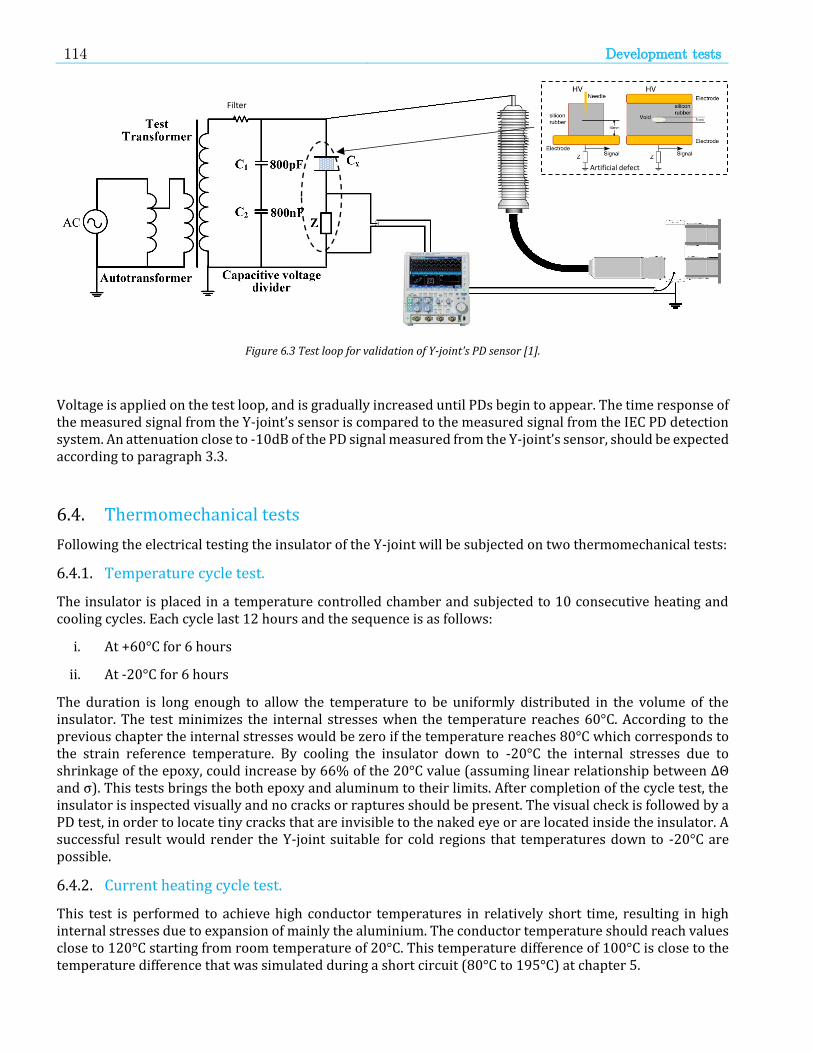
114 Development tests
Figure 6.3 Test loop for validation of Y-joint's PD sensor [1].
Voltage is applied on the test loop, and is gradually increased until PDs begin to appear. The time response of the measured signal from the Y-joint’s sensor is compared to the measured signal from the IEC PD detection system. An attenuation close to -10dB of the PD signal measured from the Y-joint’s sensor, should be expected according to paragraph 3.3.
6.4. Thermomechanical tests
Following the electrical testing the insulator of the Y-joint will be subjected on two thermomechanical tests:
6.4.1. Temperature cycle test.
The insulator is placed in a temperature controlled chamber and subjected to 10 consecutive heating and cooling cycles. Each cycle last 12 hours and the sequence is as follows:
i. At +60°C for 6 hours
ii. At -20°C for 6 hours
The duration is long enough to allow the temperature to be uniformly distributed in the volume of the insulator. The test minimizes the internal stresses when the temperature reaches 60°C. According to the previous chapter the internal stresses would be zero if the temperature reaches 80°C which corresponds to the strain reference temperature. By cooling the insulator down to -20°C the internal stresses due to shrinkage of the epoxy, could increase by 66% of the 20°C value (assuming linear relationship between ΔΘ and σ). This tests brings the both epoxy and aluminum to their limits. After completion of the cycle test, the insulator is inspected visually and no cracks or raptures should be present. The visual check is followed by a PD test, in order to locate tiny cracks that are invisible to the naked eye or are located inside the insulator. A successful result would render the Y-joint suitable for cold regions that temperatures down to -20°C are possible.
6.4.2. Current heating cycle test.
This test is performed to achieve high conductor temperatures in relatively short time, resulting in high internal stresses due to expansion of mainly the aluminium. The conductor temperature should reach values close to 120°C starting from room temperature of 20°C. This temperature difference of 100°C is close to the temperature difference that was simulated during a short circuit (80°C to 195°C) at chapter 5.
Filter
Artificial defect

115 Development tests
The testing loop consists of three insulators connected in series as shown at figure 6.4. In this way all three possible current paths are tested. Temperature sensors are placed at the click-fit ends. The complete cycle lasts 12 hours and the current transformer is controlled in the following way:
1. Current is ON for 4 hours. A conductor temperature of 120°C must be achieved and maintained during this period. The ON current value is estimated close to 2600 A.
2. Current is OFF for the next 8 hours, to allow the insulators to naturally cool down to room temperature.
Although the heating duration is small, is not small enough to make the process adiabatic as in the case of the short circuit. Nevertheless, it is a recommendable development test that gives rise to thermal stresses from an internal heat source.
The test certificates per component are show at the following pages:
Figure 6.4 Heating cycle test loop.

116 Development tests

117 Development tests

118 Development tests

7 7. Conclusions & future scope
The main goal of this thesis was the design of a 72 kV three cable joint, or CFJY-72 (Y-joint), for the upcoming needs of the offshore wind industry market, considering the upgrade from 33 kV to 66 kV of wind farm’s inter-array grid. As part of a complete solution (cable and accessories) the CFYJ-72 will offer significant cost reduction in switching facilities. The report focused on the analysis of the electrical, thermal and mechanical behaviour of the Y-joint under severe loading conditions. Furthermore, due to its strategic position in the HV voltage system (circuit node of three branches), and due to the number of different insulation interfaces, the feasibility of integrating a partial discharge sensor in the epoxy insulator was examined.
The fact that the geometry of this component is different than the usual coaxial geometry of almost all cable accessories, lead to a new approach in the design process. In this approach the use of finite element analysis tools is utilized in great extend to evaluate the behaviour of the accessory under electrical, thermal and mechanical stressing conditions. Each type of stressing was investigated in a separate chapter of the report. The chapter began with a theoretical introduction of the involved physics and was followed by the problem formulation and investigation proposal. Then the simulation results were presented and compared with the anticipated values.
7.1. Concluding remarks on the simulation results
The end result gives a design of a robust and “smart” 72.5 kV Y-joint, able to meet all requirements set by the relevant standards. From an electrical point of view it proved to be a safe design with limited risk of electrical breakdown while maintaining a very compact profile. The high dielectric withstand capability of epoxy allows the integration of a high frequency PD sensor, realized by means of a capacitive coupler. Furthermore, its thermal behavior showed that it can withstand high currents and can thus be connected with the largest cross-sections of this voltage class. The short circuit withstand capability was examined from a thermal stress perspective and it was found that the critical temperature of the insulator’s conductor due to thermal expansion is 195°C. This temperature limit gives the allowable value and duration of the short circuit current rating. The mechanical analysis of the insulator under uniaxial compressive/tensile and cantilever forces, showed that the insulator is capable of withstanding thermomechanical forces produced by the cable connections on the accessory in a rigid construction. At last the shrinkage stresses during the production phase are not point of concern since they remain at low values.
More specifically:
Electrical field - The maximum electrical field in epoxy is located at the conical parts of the insulator and is 63% of the permissible field, posing no breakdown risk for the component. The electrical field at the horizontal part of the conductor and on the M8 inserts is almost half of the permissible value.The rubber’s stress cone (at the epoxy side) was redesigned with a profile that allows the electrode to overlap with the end of the insulators zinc coating. The new profile has an effect on 1) the electrical field in epoxy, 2) the electrical field in Si and 3) the tangential field at the Si-epoxy
120 Conclusions & future scope
interface. The results of the simulation show that the insulating materials and interfaces are stressed below the permissible values. Consequently, the design of the stress cone is acceptable. The conclusion is that the electrical components (i.e. insulator and rubber parts) can be electrically tested up to the standardized voltage values for short duration AC 50Hz and lightning impulse.
Temperature distribution: The highest conductor temperature within the Y-joint is located inside the rubber part. The conductor at the epoxy part has 10 -20°C lower maximum temperature due to 1) the good thermal conductivity of epoxy compared to rubber, 2) the large contact surface with the aluminium flange and 3) the presence of the 3rd unloaded cable. The last two act as a heat sink, improving the heat dissipation capability of the Y-joint. Cables of 1600 mm2 Al and 1200 mm2 Cu can be connected to the Y-joint without conductor temperatures exceeding 90°C in steady state conditions. At last, during IEC cycle loading, the Y-joint does not reach high temperatures and cools down to room temperature within 16h.
Short circuit withstand capability: The limitations are set by the developing cantilever forces as well as by the thermal stresses due expansion of the conductor assuming adiabatic temperature rise. Both current value and short circuit duration are important and so an I-t withstand curve is calculated.
Strength under thermomechanical forces from connected cables: It was found that the main limitation comes from the M8 steel bolts that are fixing the insulator on the aluminium plate. These bolts are pre-stressed after been screwed in place, thus their yield strength is easier achieved under pull-out forces. More specifically, the withstand capability of the Y-joint under tensile-compressive forces is limited at 34.5 kN (at -z direction) for leg 2 and also along the axis of leg 1 and leg 3.
Stresses during production: The higher coefficient of thermal expansion for epoxy compared to aluminum results in stresses when the insulator is cooled down from 80°C to 20°C, but remain at safe levels.
7.2. Recommendation for future research
As already mentioned, the Y-joint introduces a new concept for the high voltage cable systems. New possibilities as well as new risks may arise as a result of installing such component in the network:
The Y-joint offers great cost savings in electrical equipment and especially on switchgear facilities within a windfarm. Nevertheless, by removing a switchgear unit from the grid the inability to isolate faults in a small section of the inter-array cable or disconnect specific parts of the inter-array line for maintenance reasons, will increase the average “off-line” time per wind turbine. In this case, installing Y-joint connections in every wind turbine is the worst option in terms of cost from production loss due to line outage. The safest solution would be to install inter-array switchgear in every wind turbine, but this solution would increase significantly the investment cost. Of course, the probability of a fault in an offshore wind farm can be low, thus not justifying the huge investment in switchgear facilities. A study can be performed in order to find the fine balance between those parameters and strategically place switchgear units in the electrical topology of the windfarm while utilizing the cost effective solution of the Y-joint.
The integrated PD sensor, adds value to the Y-joint as well as to the system it is installed in. Assuming that many Y-joints of this type are installed in an offshore windfarm, they could be part of a greater monitoring system that can detect and locate faults before they occur. Special algorithms could be developed, that are able to detect the path of the PD pulses through the grid via the Y-joints’ detectors. Furthermore, depending on the topology of the wind farm, Y-joints with integrated PD sensor could be installed in wind turbines with strategic position in the grid. In this way, the concept of an offshore smart grid, in terms of self-protection, is feasible.

121 APPENDIX A1
APPENDIX A1 - Calculation of capacitance via FEA
The Comsol electrostatics module can calculate the capacitance of the simulation arrangement. The variable
called es.C11 corresponds to the capacitance of the terminal (HV electrode) to ground. When a floating
electrode is present in the arrangement, then this value(es.C11) takes into account also the capacitances of
a) the floating electrode to ground and b) the floating electrode to the HV part. These capacitances are not
explicitly calculated by Comsol and must be derived in a different
way.
A simple geometry of 3 parallel discs is created in order to
demonstrate the method of defining these capacitances. The discs
have R=10 cm, thickness 1mm and each has 1.8 cm distance from
the one next by it. The discs will be named 1, 2 and 3 starting from
the top one. The capacitances for εr=4.5 can theoretically
calculated as:
𝐶12 = 𝐶23 = 휀𝜊휀𝑟
𝜋𝑅2
𝑑= 0.0695 𝑛𝐹
1st scenario – Top disk energized, middle disk floating, bottom disk grounded
Comsol calculates the es.C11 value corresponding to the capacitance of the energized part to ground. Actually
it is C13 in parallel with the series connection of C12 and C23 . The related equation is:
𝑒𝑠. 𝐶11 = 𝐶13 +𝐶12𝐶23
𝐶12+𝐶23= 0.051452𝑛𝐹 (1)
2nd scenario – Top disk energized, middle disk grounded, bottom disk floating
Comsol calculates the es.C11 value corresponding to the capacitance of the energized part to ground. Actually
it is C12 in parallel with the series connection of C13 and C23 . The related equation is:
𝐶12 +𝐶13𝐶23
𝐶13+𝐶23= 0.087321𝑛𝐹 (2)
3rd scenario – Top disk floating, middle disk energized, bottom disk grounded
Comsol calculates the es.C11 value corresponding to the capacitance of the energized part to ground. Actually
it is C23 in parallel with the series connection of C13 and C12 . The related equation is:
𝐶23 +𝐶13𝐶12
𝐶13+𝐶12= 0.087322𝑛𝐹 (3)
By solving the system of 3 equations we get the capacitances between each of the discs:
𝐶23 = 0.075838𝑛𝐹
𝐶12 = 0.075837𝑛𝐹
𝐶13 = 0.013533𝑛𝐹
The first two capacitances are close to the theoretical calculations. They are not exact because the FEM
calculates also the fringing capacitances from the edges of the discs. So the method is valid and can be used
in the Y-joint model to find the related capacitances of the floating electrode to ground and to the HV
conductor.
1
2
3

122 APPENDIX A2
APPENDIX A2 - MATLAB scripts
Code for computing capacitances: clear C13 C12 C23
syms C13 C12 C23 C_comsol1 C_comsol2 C_comsol3
%% FEM capacitance values calculated for each scenario
C_comsol1=0.13987;
C_comsol2=0.07184;
C_comsol3=0.089264;
%% Solution of the system of equations to ide
% [solx,soly,solz] = solve(a*y+a*z == b*x+b*z, a*y+a*z == c*x+c*y, b*x+b*z == c*x+c*y)
S = solve(C_comsol1==C13+C12*C23/(C12+C23), C_comsol2== C12+C13*C23/(C13+C23), C_comsol3==C23+C13*C12/(C13+C12));
C_HVtoGround=vpa(S.C13)
C_SensortoHV=vpa(S.C12)
C_SensortoGround=vpa(S.C23)
Code for extracting the frequency characteristics of the capacitive coupler %% Bode diagram of the HF capacitive coupler
%% Intitialization
clear all
opts = bodeoptions('cstprefs');
opts.PhaseVisible = 'off';
opts.FreqUnits = 'Hz';
f=10.^(1:0.01:9); %frequency spectrum [Hz]
w=2*pi*f;
%% RLC circuit parameters
R=4600; %Resistance value [Ohm]
L=0.4*1e-3; %Inductance value [H]
C1 = 52*10.^(-12); %capacitance electrode to HV [F]
C2 = (10+55)*10.^(-12); %capacitance to ground [F]
%% Bode diagram of the transfer function object
H = tf( [(R*L)^2*C1*C2 R*L^2*C1 R^2*L*C1 0 0] , [(R*L)^2*C2*(C1+C2) 2*R*L^2*C2+R*L^2*C1 R^2*L*(C1+C2)+L^2 2*L*R R^2]);
[mag,phase] = bode(H,w);
magdb = 20*log10(mag);
for i= 1:length(f)
magdb1(i)=magdb(:,:,i);
end
%% Basic frequency response's characteristics
flat=magdb(1,1,length(f)); %attenuation at the flat region of the bode diagram
f3db=f(find(abs(magdb(1,1,:)+3-flat)<1)) % cut-off frequency at -3db
G50hz=magdb(find(abs(f-50)<0.5)) % attenuation of 50Hz signal
%% plot bode diagram
figure
% Create semilogx
semilogx(f,magdb1,'LineWidth',1.5,'DisplayName','1 insert');
% Create title
title(['R=' num2str(R) ' kΩ , L=' num2str(1000*L) 'mH, C_1=' num2str(C1*1e12) 'pF, C_2=' num2str(C2*1e12) 'pF']);
% Create xlabel
xlabel('Frequency (Hz)');

123 APPENDIX A2
% Create ylabel
ylabel('20log(V_{out}/V_{in}) [dB]');
axis([0 1e9 -200 0]);
box on;
grid on;
Code for creating the PD pulse from Gaussian function %% Ploting the positive pulse from needle defect in time and frequency domain
%% Initialization
clear all
t_start=0;
t_end=100e-9;
rate=0.1e-9;
t=t_start:rate:t_end;
b=zeros(length(t),2);
t_inc=0+t;
%% Gaussian sub-pulse parameters
A1=2.44e-9;
A2=2.54e-9;
A3=-1.65e-9;
A4=-0.72e-9;
A5=0.55e-9;
W1=1.91e-9;
W2=2.65e-9;
W3=1.97e-9;
W4=2.23e-9;
W5=2.78e-9;
Xc1=40.3e-9;
Xc2=44.8e-9;
Xc3=45.8e-9;
Xc4=49.4e-9;
Xc5=55.1e-9;
%% PD pulse from Gaussian function
y=A1/(W1*sqrt(pi/2))*exp(-2*((t-Xc1)/W1).^2)+...
A2/(W2*sqrt(pi/2))*exp(-2*((t-Xc2)/W2).^2)+...
A3/(W3*sqrt(pi/2))*exp(-2*((t-Xc3)/W3).^2)+...
A4/(W4*sqrt(pi/2))*exp(-2*((t-Xc4)/W4).^2)+...
A5/(W5*sqrt(pi/2))*exp(-2*((t-Xc5)/W5).^2);
%% Exporting the PD signal into a txt file for input at pspice
a=y.';
b(:,1)=t_inc.';
b(:,2)=a;
dlmwrite('pdsignal.txt',b,'delimiter','\t','precision','%.10f');
%% Frequency spectrum
Fs = 1/rate;
n = 2^nextpow2(length(t));
Y = fft(y,n);
f = Fs*(0:(n/16))/n;
P = abs(Y/n);
%% Plot pulse at time domain
figure
plot(t*1e9,y)
xlabel('time [ns]');
ylabel('Voltage [pu]');
box on;
grid on;
%% Plot pulse at frequency domain
figure
plot(f*1e-6,P(1:n/16+1));
title('Gaussian Pulse in Frequency Domain')
xlabel('Frequency (MHz)')
ylabel('|P(f)|')

124 APPENDIX A2
box on;
grid on;
Code for creating the lightning impulse %% Ploting the lightning impulse in time and frequency domain
%% Initialization
t_start=0;
t_end=400e-6;
rate=1e-7;
t=t_start:rate:t_end;
b=zeros(length(t),2);
%% Standard impulse 1.2/50us wave
A=325*1e3; % 325kV BIL
Tf=1.2e-6; % front time
Th=50e-6; % 50% decay time
tau1=Th/0.73;
tau2=Tf/2.96;
y=1.04*A*(exp(-t./tau1)-exp(-t./tau2)); %pulse in pu
%% Exporting the PD signal into a txt file for input at pspice
a=y.';
b(:,1)=t';
b(:,2)=a;
dlmwrite('impulse.txt',b,'delimiter','\t','precision','%.10f');
%% Frequency spectrum
Fs = 1/rate;
n = 2^nextpow2(length(t));
Y = fft(y,n);
f = Fs*(0:(n/8))/n;
P = abs(Y/n);
%% Plot pulse at time domain
figure
plot(t*1e6,y)
xlabel('time [us]');
ylabel('Voltage [kV]');
box on;
grid on;
%% Plot pulse at frequency domain
figure
plot(f*1e-3,P(1:n/8+1))
title('Gaussian Pulse in Frequency Domain')
xlabel('Frequency (kHz)')
ylabel('|P(f)|')

125 APPENDIX B
APPENDIX B - Thermomechanical forces from cables
This appendix deals with the calculation of compressive/tensile thermomechanical forces of common high
voltage cable constructions. These forces are representative of rigidly fixed cables.
Table 5.12 Tensile/Compressive forces in Nt from cables with aluminum conductor and aluminum sheath.
Conductor area
[mm2]
240 300 400 500 630 800 1000 1200 1600
Metallic sheath
area
[mm2]
28 9803 11945 15515 19085 23726 29795 36935 44075 58355
50 10773 12915 16485 20055 24696 30765 37905 45045 59325
61 11258 13400 16970 20540 25181 31250 38390 45530 59810
70 11655 13797 17367 20937 25578 31647 38787 45927 60207
95 12758 14900 18470 22040 26681 32750 39890 47030 61310
115 13640 15782 19352 22922 27563 33632 40772 47912 62192
Table 5.13 Tensile/Compressive forces in Nt from cables with aluminum conductor and lead sheath.
Conductor area
[mm2]
240 300 400 500 630 800 1000 1200 1600
Metallic sheath
area
[mm2]
28 8849 10991 14561 18131 22772 28841 35981 43121 57401
50 9069 11211 14781 18351 22992 29061 36201 43341 57621
61 9180 11322 14892 18462 23103 29172 36312 43452 57732
70 9270 11412 14982 18552 23193 29262 36402 43542 57822
95 9520 11662 15232 18802 23443 29512 36652 43792 58072
115 9721 11863 15433 19003 23644 29713 36853 43993 58273
Table 5.14 Tensile/Compressive forces in Nt from cables with copper conductor and lead sheath.
Conductor area
[mm2]
240 300 400 500 630 800 1000 1200 1600
Metallic sheath
area
[mm2]
28 7355 9738 12686 15634 19466 24477 30373 36268 48059
50 7576 10441 13389 16337 20169 25180 31076 36971 48762
61 7686 10792 13740 16688 20520 25531 31427 37323 49114
70 7777 11080 14028 16976 20808 25819 31715 37610 49401
95 8027 11879 14826 17774 21606 26618 32513 38409 50200
115 8228 12518 15465 18413 22245 27257 33152 39048 50839

126 APPENDIX B

127 Bibliography
Bibliography
[1] ECN, PBL Netherlands Environmental Assesment Agency, Statistics Nethrlands, Netherlands
Enterprise Agency, “Netherlands National Energy Outlook 2014”.
[2] Netherlands Enterprise Agency, Offshore wind energy in the Netherlands - The roadmap from
1000MW to 4.500MW offshore wind capacity.
[3] DNV-GL report 113799-UKBR-R02, Rev. 2, TENNET, NL OFFSHORE WIND FARM
TRANSMISSION SYSTEMS - 66kV Systems for Offshore Wind Farms, 2015
[4] Prysmian brochure “66kV offshore wind farm cable accessories”.
[5] Prysmian group, “Accessories for underground and submarine systems”.
[6] K Ohata, T. Goto, M. Yamashita and M. Sakamaki, “Development of Y-branch joint for 275-kV
XLPE and fluid-filled cable”, Transmission and distribution Conference and Exhibition 2002: Asia
Pacific IEEE/PES.
[7] IEC Task Force 21(B1)-10, “Thermal ratings of HV cable accessories”, Electra No 212 February
2004.
[8] Y. Tian, P.L. Lewin, A.E. Davies, S.G. Swingler, S. J. Sutton G. M. Hathaway, “ Comparison of
On-line Partial Discharge Detection Methods for HV Cable Joints”, IEEE Transactions on
Dielectrics and Electrical Insulation, 2002.
[9] New Partial Discharge Detection Method for Live UHV/EHV Cable Joints
[10] Sheppard Salon, M. V.K. Chari Numerical Methods in Electromagnetism 1999
[11] F.H. Kreuger, Industrial high voltage - Part I, Delft University press 1991
[12] F.H. Kreuger, Industrial high voltage - Part II, Delft University press 1992
[13] IEC 60840, Power Cables With extruded Insulation and their Accessories for rated voltages above
30kV(Um=36kV) up to 150kV(Um=170kV)-Test methods and requirements, edition 4.0, 2011.
[14] IEC 60137, ed.6 2008-07, Insulated bushings for alternating voltages above 1000V.
[15] IEEE Power & Energy Society, “IEEE Recommended Practice for Partial Discharge Measurement
in Liquid-Filled Power Transformers and Shunt Reactors”.
[16] DNV_GL Standard, DNVGL-ST-0076, “Design of electrical installations for wind turbines”,
Edition May 2015.
[17] COMSOL multiphysics, “User’s guide -AC/DC module”, version May 2011.
[18] Comission, I. E. (2000). IEC 60270: High-Voltage Test Techniques - Partial Discharge
Measurements, 44.
[19] A.Rodrigo Mor, Llovera, P., Fuster, V., & Quijano, A. (2013), “High performance broadband
capacitive coupler for partial discharge cable tests”, IEEE Transactions on Dielectrics and
Electrical Insulation, 20(2), 479–487.
128 Bibliography
[20] Ma, G.-M., Li, C.-R., Chen, X.-W., Jiang, J., Ge, Z.-D., & Chang, W.-Z. (2015), “Numerical sensor
design for partial discharge detection on power cable joint”, IEEE Transactions on Dielectrics and
Electrical Insulation, 22(4), 2311–2319.
[21] Y. Tian, P.L. Lewin, A.E. Davies, S.G. Swingler, S. J. Sutton G. M. Hathaway, “ Comparison of
On-line Partial Discharge Detection Methods for HV Cable Joints”, IEEE Transactions on
Dielectrics and Electrical Insulation, 2002.
[22] Heizmann, T., Aschwanden, T., Hahn, H., Laurent, M., & Ritter, “ On-site partial discharge
measurements on premoulded cross-bonding joints of 170 kV XLPE and EPR cables”, IEEE
Transactions on Power Delivery, 13(2), 330–335, April 1998.
[23] Lee, C. Y., Nam, S. H., Lee, S. G., Kim, D. W., & Choi, , “High frequency Partial Discharge
measurement by capacitive sensor for underground power cable system”, PowerCon 2000 - 2000
International Conference on Power System Technology, Proceedings, 3, 1517–1520.
[24] Illias, H. A., Yon, H. R., Mokhlis, H., Chen, G., Lewin, P. L., & Ariffin, “Modelling of partial
discharge pulses in high voltage cable insulation using finite element analysis software”, Electrical
Insulation Conference, Ottawa, Ontario, Canada, 2 to 5 June 2013.
[25] Fukunaga, K., & Tan, M. “New Partial Discharge Detection Method for Live UHV/EHV Cable
Joints” IEEE Transactions on Electrical Insulation, Vol. 27 No. 3, June 1992.
[26] IEEE Power & Energy Society, “IEEE Recommended Practice for Partial Discharge Measurement
in Liquid-Filled Power Transformers and Shunt Reactors”.
[27] A.Rodrigo Mor, P.H.F. Morshuis, J.J. Smit, “Comparison of charge estimation methods in partial
discharge cable measurements”, IEEE Transactions on Dielectrics and Electrical Insulation 22 (2),
657-664.
[28] J. A. Pilgrim, D. J. Swaffield, P. L. Lewin, S.T. Larsen and D. Payne, “Assessment of the Impact
of Joint Bays on the Ampacity of High-Voltage Cable Circuits”, IEEE transactions on power
delivery,vol.24, no.3, July 2009.
[29] Pilgrim, J. A., Swaffield, D. J., Lewin, P. L., Larsen, S. T., & Payne, “ Use of finite element analysis
to obtain thermal ratings for high voltage cable joint bays” 2009 IEEE Electrical Insulation
Conference, EIC 2009, (June), 224–227.
[30] AORC Technical meeting 2014, B1-1083, “Cable System Failure Experience in Wind Farms”
[31] Pilgrim, J. A., Swaffield, D. J., Lewin, P. L., & Payne, D. (2008), “An investigation of thermal
ratings for high voltage cable joints through the use of 2D and 3D Finite Element Analysis”,
Conference Record of IEEE International Symposium on Electrical Insulation, 543–546.
[32] George J. Anders, “Rating of Electric Power Cables in Unfavorable Thermal Environment”, IEEE
Press, John Wiley & Sons, Inc. , Publication.
[33] COMSOL multiphysics User’s guide
[34] IEC 60287, ed.1.2 2001-11,Part 1.1-1.3, “Calculation of the current rating”.
[35] G.F. Moore, “ Electric cables Handbook”, 3rd edition, Blackwell Science 1997
[36] Liang, Y., “Steady-state thermal analysis of power cable systems in ducts using streamline-
upwind/Petrov-Galerkin finite element method”, IEEE Transactions on Dielectrics and Electrical
Insulation, 19(1), 283–290.

129 Bibliography
[37] G.F. Moore, “ Electric cables Handbook”, 3rd edition, Blackwell Science 1997.
[38] Keith D. Hjelmstad, “Fundamentals of Structural Mechanics”, 2nd Edition, Springer, ISBN 0-387-
23330-X.
[39] Dr. A.B. Zavatsky, “ P4 Stress and Strain- Lecture 5 - Plane Stress Transformation Equations”.
[40] D. Chapman, Prof. T. Norris, “ Copper for bus-bars- 4.0 Short-Circuit Effects”
[41] “Lecture 5- Stress-Strain material laws”, Course “Introduction to aerospace structures”, University
of Colorado.
[42] “Derivation of the von Mises criterion”, Course “Aerospace structures”, University of Florida.
[43] Epoxy technology Epotek, “ Bonding to aluminum - Tech tip 24”.
[44] Wikipedia Stress-strain curve: https://en.wikipedia.org/wiki/Stress%E2%80%93strain_curve
[45] Wikipedia Von Mises yield criterion: https://en.wikipedia.org/wiki/Von_Mises_yield_criterion
[46] Prysmian Cables and Systems, Report : “High voltage isolator- Simulations 2x scaled design”
[47] Inductance calculation formulas: http://www.rfcafe.com/references/electrical/inductance.htm.


