Package / Module / PC Card Outlines and Dimensions 2 · PD PE Q R S SB SM U X ... Acronym C-PGA or...
76
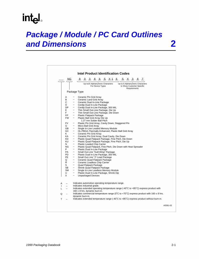
1999 Packaging Databook 2-1 Package / Module / PC Card Outlines and Dimensions 2 A5581-02 Intel Product Identification Codes NG Package Type A I L Q T A B C D DP E F FP FW FV G GB GC K KA KD KU N NG P PA PD PE Q R S SB SM U X – – – – – – – – – – – – – – – – – – – – – – – – – – – – – – Indicates automotive operating temperature range. Indicates industrial grade. Indicates extended operating temperature range (-40˚C to +85˚C) express product with 160 ± 8 hrs. dynamic burn-in. Indicates commercial temperature range (0˚C to +70˚C) express product with 160 ± 8 hrs. dynamic burn-in. Indicates extended temperature range (-40˚C to +85˚C) express product without burn-in. Ceramic Pin Grid Array Ceramic Land Grid Array Ceramic Dual In-Line Package Cerdip Dual In-Line Package Cerdip Dual In-Line Package, 300 MIL Thin Small Out-Line Package, Die Up Thin Small Out-Line Package, Die Down Plastic Flatpack Package Plastic Ball Grid Array Die Up 1.27 mm Solder Ball Pitch Plastic Pin Grid Array, Cavity Down, Staggered Pin Micro Ball Grid Array Single In-Line Leaded Memory Module HL-PBGA-Thermally Enhanced, Plastic Ball Grid Array Ceramic Pin Grid Array Ceramic Pin Grid Array, Dual Cavity, Die Down Plastic Quad Flatpack Package, Fine Pitch, Die Down Plastic Quad Flatpack Package, Fine Pitch, Die Up Plastic Leaded Chip Carrier Plastic Quad Flatpack, Fine Pitch, Die Down with Heat Spreader Plastic Dual In-Line Package Small Out-Line "Gull-Wing" Package Plastic Dual In-Line Package, 300 MIL Small Out-Line "J"-Lead Package Ceramic Quad Flatpack Package Ceramic Leadless Chip Carrier Quad Flatpack Package Shrink Quad Flatpack Package Single In-Line Leadless Memory Module Plastic Dual In-Line Package, Shrink Dip Unpackaged Devices 8 0 3 8 6 S X 1 6 S X 3 8 7 Up to15 Alphanumeric Characters For Device Types Up to 6 Alphanumeric Characters to Show Customer-Specific Requirements _ _ _ _ _
Transcript of Package / Module / PC Card Outlines and Dimensions 2 · PD PE Q R S SB SM U X ... Acronym C-PGA or...
Package / Module / PC Card Outlines and Dimensions 2
A5581-02
Intel Product Identification Codes
NG
Package Type
AIL
Q
T
ABCDDPEFFPFW
FVGGBGCKKAKDKUNNGPPAPDPEQRSSBSMUX
–––––––––
–––––––––––––––––––––
Indicates automotive operating temperature range.Indicates industrial grade.Indicates extended operating temperature range (-40˚C to +85˚C) express product with160 ± 8 hrs. dynamic burn-in.Indicates commercial temperature range (0˚C to +70˚C) express product with 160 ± 8 hrs.dynamic burn-in.Indicates extended temperature range (-40˚C to +85˚C) express product without burn-in.
Ceramic Pin Grid ArrayCeramic Land Grid ArrayCeramic Dual In-Line PackageCerdip Dual In-Line PackageCerdip Dual In-Line Package, 300 MILThin Small Out-Line Package, Die UpThin Small Out-Line Package, Die DownPlastic Flatpack PackagePlastic Ball Grid Array Die Up 1.27 mm Solder Ball PitchPlastic Pin Grid Array, Cavity Down, Staggered PinMicro Ball Grid ArraySingle In-Line Leaded Memory ModuleHL-PBGA-Thermally Enhanced, Plastic Ball Grid ArrayCeramic Pin Grid ArrayCeramic Pin Grid Array, Dual Cavity, Die DownPlastic Quad Flatpack Package, Fine Pitch, Die DownPlastic Quad Flatpack Package, Fine Pitch, Die UpPlastic Leaded Chip CarrierPlastic Quad Flatpack, Fine Pitch, Die Down with Heat Spreader Plastic Dual In-Line PackageSmall Out-Line "Gull-Wing" PackagePlastic Dual In-Line Package, 300 MILSmall Out-Line "J"-Lead PackageCeramic Quad Flatpack PackageCeramic Leadless Chip CarrierQuad Flatpack PackageShrink Quad Flatpack PackageSingle In-Line Leadless Memory ModulePlastic Dual In-Line Package, Shrink DipUnpackaged Devices
8 0 3 8 6 S X 1 6 S X 3 8 7
Up to15 Alphanumeric CharactersFor Device Types
Up to 6 Alphanumeric Charactersto Show Customer-Specific
Requirements
___
_
_
1999 Packaging Databook 2-1
Package / Module / PC Card Outlines and Dimensions
2.1 Ceramic Side Braze Dual In-line Package
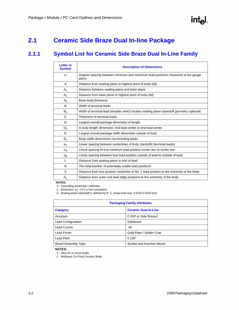
2.1.1 Symbol List for Ceramic Side Braze Dual In-Line Family
Letter or Symbol Description of Dimensions
α Angular spacing between minimum and maximum lead positions measured at the gauge plane
A Distance from seating plane to highest point of body (lid)
A1 Distance between seating plane and base plane
A2 Distance from base plane to highest point of body (lid)
A3 Base body thickness
B Width of terminal leads
B1 Width of terminal lead shoulder which locates seating plane (standoff geometry optional)
C Thickness of terminal leads
D Largest overall package dimension of length
D2 A body length dimension, end lead center to end lead center
E Largest overall package width dimension outside of lead
E1 Body width dimensions not including leads
e1 Linear spacing between centerlines of body standoffs (terminal leads)
eA Linear spacing of true minimum lead position center line to center line
eB Linear spacing between true lead position outside of lead to outside of lead
L Distance from seating plane to end of lead
N The total number of potentially usable lead positions
S Distance from true position centerline of No. 1 lead position to the extremity of the body
S1 Distance from outer end lead edge positions to the extremity of the bodyNOTES: 1. Controlling dimension: millimeter.2. Dimension “e1” (“e”) is non-cumulative.3. Seating plane (standoff) is defined by P. C. board hole size: 0.0415-0.0430 inch.
Packaging Family Attributes
Category Ceramic Dual-In-Line
Acronym C-DIP or Side Brazed
Lead Configuration Sidebraze
Lead Counts 40
Lead Finish Gold Plate / Solder Coat
Lead Pitch 0.100”
Board Assembly Type Socket and Insertion Mount
NOTES:1. Alloy 42 or Kovar leads. 2. Multilayer Co-Fired Ceramic Body.
2-2 1999 Packaging Databook
Package / Module / PC Card Outlines and Dimensions
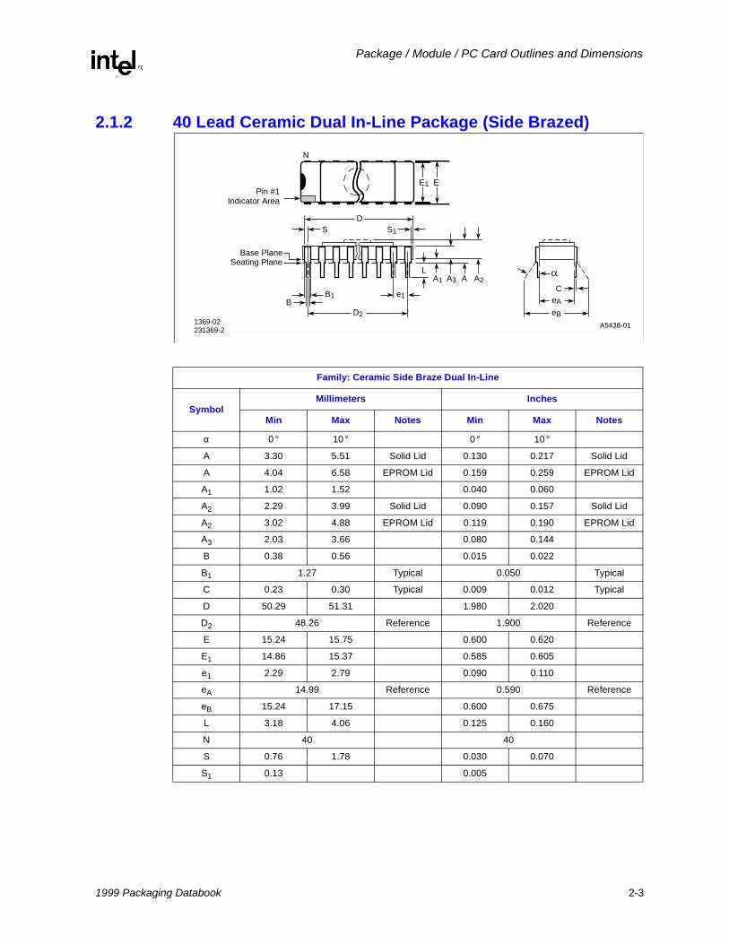
2.1.2 40 Lead Ceramic Dual In-Line Package (Side Brazed)
A5438-01
N
EE1Pin #1
Indicator Area
e1B
B1
D2
DS S1
Seating PlaneBase Plane
LA1 A2A3 A
eB
eA
C
1369-02231369-2
Family: Ceramic Side Braze Dual In-Line
SymbolMillimeters Inches
Min Max Notes Min Max Notes
α 0 ° 10 ° 0 ° 10 °
A 3.30 5.51 Solid Lid 0.130 0.217 Solid Lid
A 4.04 6.58 EPROM Lid 0.159 0.259 EPROM Lid
A1 1.02 1.52 0.040 0.060
A2 2.29 3.99 Solid Lid 0.090 0.157 Solid Lid
A2 3.02 4.88 EPROM Lid 0.119 0.190 EPROM Lid
A3 2.03 3.66 0.080 0.144
B 0.38 0.56 0.015 0.022
B1 1.27 Typical 0.050 Typical
C 0.23 0.30 Typical 0.009 0.012 Typical
D 50.29 51.31 1.980 2.020
D2 48.26 Reference 1.900 Reference
E 15.24 15.75 0.600 0.620
E1 14.86 15.37 0.585 0.605
e1 2.29 2.79 0.090 0.110
eA 14.99 Reference 0.590 Reference
eB 15.24 17.15 0.600 0.675
L 3.18 4.06 0.125 0.160
N 40 40
S 0.76 1.78 0.030 0.070
S1 0.13 0.005
1999 Packaging Databook 2-3
Package / Module / PC Card Outlines and Dimensions
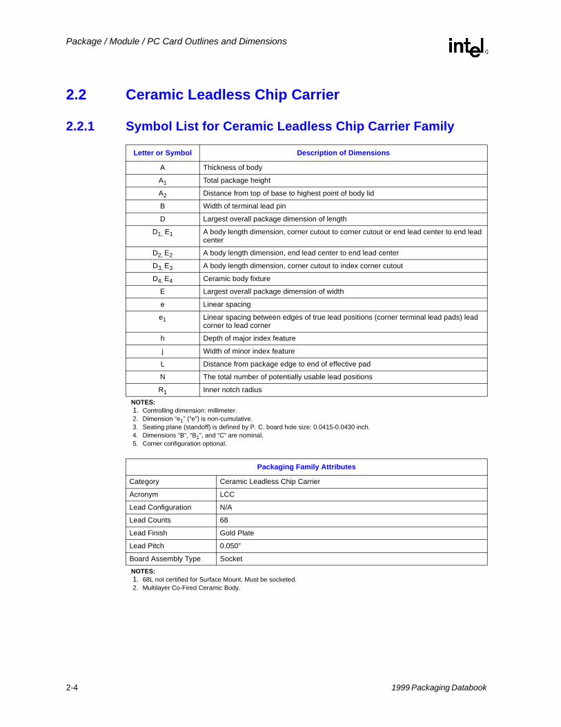
2.2 Ceramic Leadless Chip Carrier
2.2.1 Symbol List for Ceramic Leadless Chip Carrier Family
Letter or Symbol Description of Dimensions
A Thickness of body
A1 Total package height
A2 Distance from top of base to highest point of body lid
B Width of terminal lead pin
D Largest overall package dimension of length
D1, E1 A body length dimension, corner cutout to corner cutout or end lead center to end lead center
D2, E2 A body length dimension, end lead center to end lead center
D3, E3 A body length dimension, corner cutout to index corner cutout
D4, E4 Ceramic body fixture
E Largest overall package dimension of width
e Linear spacing
e1 Linear spacing between edges of true lead positions (corner terminal lead pads) lead corner to lead corner
h Depth of major index feature
j Width of minor index feature
L Distance from package edge to end of effective pad
N The total number of potentially usable lead positions
R1 Inner notch radiusNOTES: 1. Controlling dimension: millimeter.2. Dimension “e1” (“e”) is non-cumulative.3. Seating plane (standoff) is defined by P. C. board hole size: 0.0415-0.0430 inch.4. Dimensions “B”, “B1”, and “C” are nominal.5. Corner configuration optional.
Packaging Family Attributes
Category Ceramic Leadless Chip Carrier
Acronym LCC
Lead Configuration N/A
Lead Counts 68
Lead Finish Gold Plate
Lead Pitch 0.050”
Board Assembly Type SocketNOTES: 1. 68L not certified for Surface Mount. Must be socketed.2. Multilayer Co-Fired Ceramic Body.
2-4 1999 Packaging Databook
Package / Module / PC Card Outlines and Dimensions
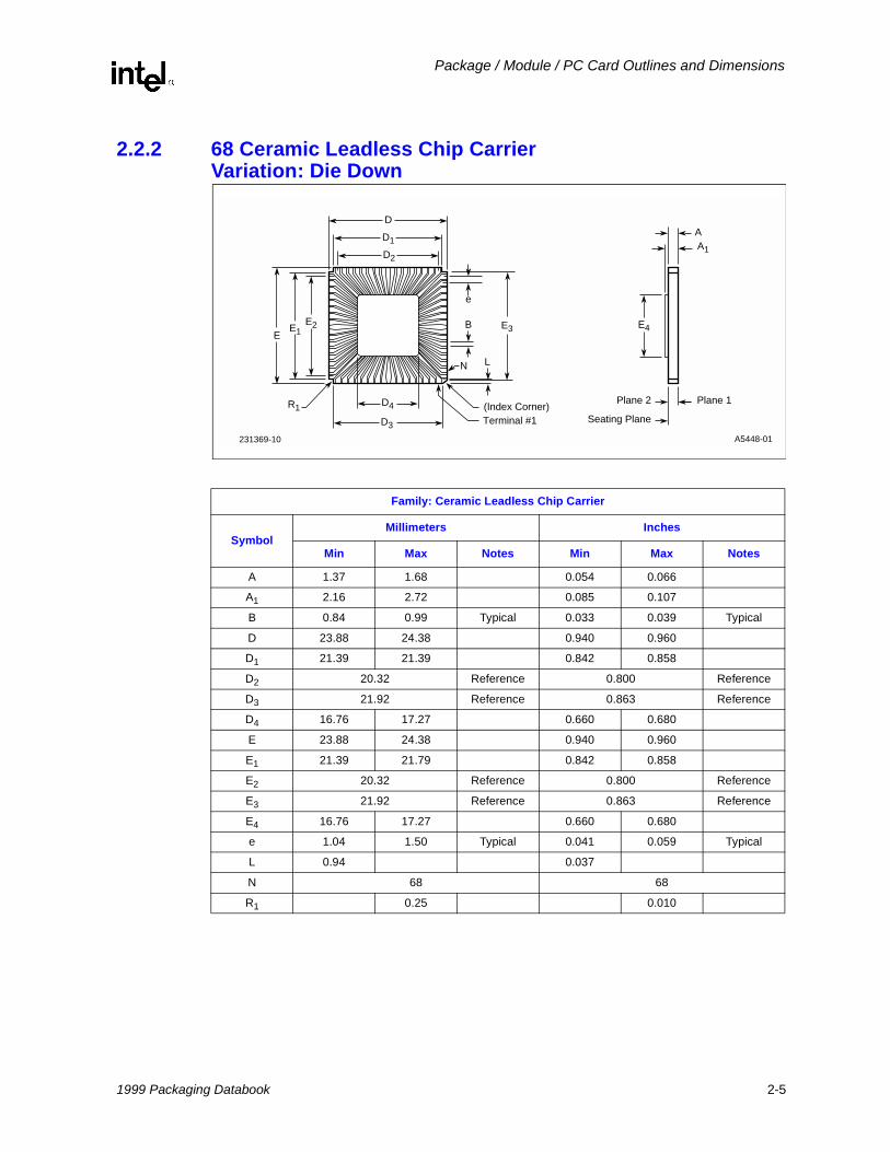
2.2.2 68 Ceramic Leadless Chip Carrier Variation: Die Down
A5448-01
A
D3
E3
R1
L
e
D
D2
D1
Terminal #1
BE
E1E2
(Index Corner)Seating Plane
Plane 1Plane 2
E4
A1
D4
N
231369-10
Family: Ceramic Leadless Chip Carrier
SymbolMillimeters Inches
Min Max Notes Min Max Notes
A 1.37 1.68 0.054 0.066
A1 2.16 2.72 0.085 0.107
B 0.84 0.99 Typical 0.033 0.039 Typical
D 23.88 24.38 0.940 0.960
D1 21.39 21.39 0.842 0.858
D2 20.32 Reference 0.800 Reference
D3 21.92 Reference 0.863 Reference
D4 16.76 17.27 0.660 0.680
E 23.88 24.38 0.940 0.960
E1 21.39 21.79 0.842 0.858
E2 20.32 Reference 0.800 Reference
E3 21.92 Reference 0.863 Reference
E4 16.76 17.27 0.660 0.680
e 1.04 1.50 Typical 0.041 0.059 Typical
L 0.94 0.037
N 68 68
R1 0.25 0.010
1999 Packaging Databook 2-5
Package / Module / PC Card Outlines and Dimensions
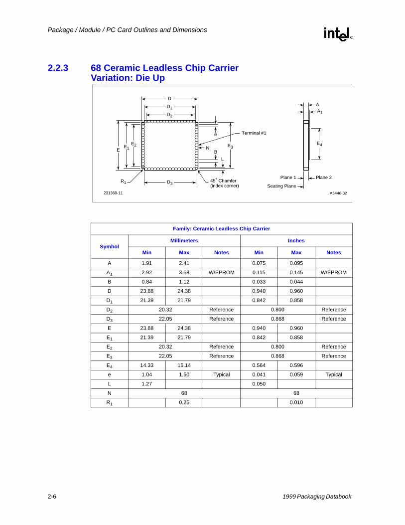
2.2.3 68 Ceramic Leadless Chip Carrier Variation: Die Up
A5446-02
A
D3
E3
L
e
D
D2
D1
N
Terminal #1
BEE1
E2
45˚ Chamfer(index corner) Seating Plane
Plane 2Plane 1
E4
A1
R1
231369-11
Family: Ceramic Leadless Chip Carrier
SymbolMillimeters Inches
Min Max Notes Min Max Notes
A 1.91 2.41 0.075 0.095
A1 2.92 3.68 W/EPROM 0.115 0.145 W/EPROM
B 0.84 1.12 0.033 0.044
D 23.88 24.38 0.940 0.960
D1 21.39 21.79 0.842 0.858
D2 20.32 Reference 0.800 Reference
D3 22.05 Reference 0.868 Reference
E 23.88 24.38 0.940 0.960
E1 21.39 21.79 0.842 0.858
E2 20.32 Reference 0.800 Reference
E3 22.05 Reference 0.868 Reference
E4 14.33 15.14 0.564 0.596
e 1.04 1.50 Typical 0.041 0.059 Typical
L 1.27 0.050
N 68 68
R1 0.25 0.010
2-6 1999 Packaging Databook

Package / Module / PC Card Outlines and Dimensions
2.3 Ceramic Pin Grid Array Package
2.3.1 Symbol List for Square Ceramic Pin Grid Array Family
Letter or Symbol Description of Dimensions
A Distance from seating plane to highest point of body
A1 Distance between seating plane and base plane
A2 Distance from base plane to highest point of body
A3 Distance from seating plane to bottom of body
A4 Heat spreader thickness
B Diameter of terminal lead pin
D Largest overall package dimension of length
D1 A body length dimension, outer lead center to outer lead center
D2 Heat spreader length and width
e1 Linear spacing between true lead position centerlines
L Distance from seating plane to end of lead
N The total number of potentially usable lead positions
S1 Other body dimension, outer lead center to edge of bodyNOTES: 1. Controlling dimension: millimeter.2. Dimension “e1” (“e”) is non-cumulative.3. Seating plane (standoff) is defined by P.C. board hole size: 0.0415 - 0.0430 inch.4. Dimensions “B”, “B1” and “C” are nominal.5. Details of Pin 1 identifier are optional
Packaging Family Attributes
Category Ceramic Pin Grid Array
Acronym C-PGA or PGA
Lead Configuration Array
Lead Counts 68, 88, 132, 168-208, 240-280, 272-320
Lead Finish Gold Plate, 60 Micro inches of Gold over 100-350 Micro inches of Nickel Plate
Lead Material Alloy 42 or Kovar
Lead Braze Material Copper/Silver Eutectic
Lead Pitch 0.100”
Board Assembly Type Socket and Insertion MountNOTES: 1. Alloy 42 or Kovar Leads.2. Multilayer Co-Fired Ceramic Body.3. Some body sizes have variable pin count.
1999 Packaging Databook 2-7
Package / Module / PC Card Outlines and Dimensions
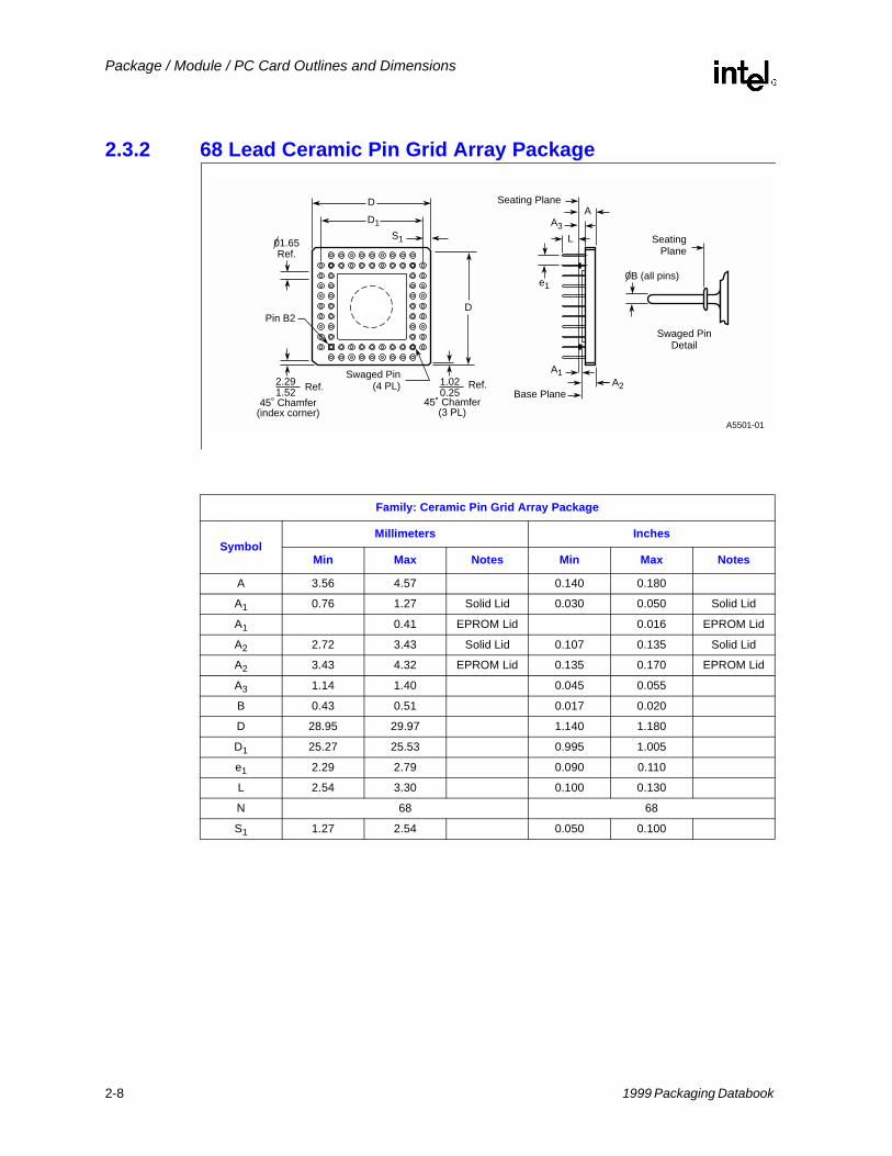
2.3.2 68 Lead Ceramic Pin Grid Array Package
A5501-01
D
A3
1.020.25
D
D1
Swaged Pin(4 PL)
Base PlaneA2
A1
e1
A
S1
Ref.
45˚ Chamfer(3 PL)
2.291.52
45˚ Chamfer(index corner)
Ref.
01.65Ref.
Pin B2
L
Seating Plane
SeatingPlane
Swaged PinDetail
0B (all pins)
Family: Ceramic Pin Grid Array Package
SymbolMillimeters Inches
Min Max Notes Min Max Notes
A 3.56 4.57 0.140 0.180
A1 0.76 1.27 Solid Lid 0.030 0.050 Solid Lid
A1 0.41 EPROM Lid 0.016 EPROM Lid
A2 2.72 3.43 Solid Lid 0.107 0.135 Solid Lid
A2 3.43 4.32 EPROM Lid 0.135 0.170 EPROM Lid
A3 1.14 1.40 0.045 0.055
B 0.43 0.51 0.017 0.020
D 28.95 29.97 1.140 1.180
D1 25.27 25.53 0.995 1.005
e1 2.29 2.79 0.090 0.110
L 2.54 3.30 0.100 0.130
N 68 68
S1 1.27 2.54 0.050 0.100
2-8 1999 Packaging Databook
Package / Module / PC Card Outlines and Dimensions
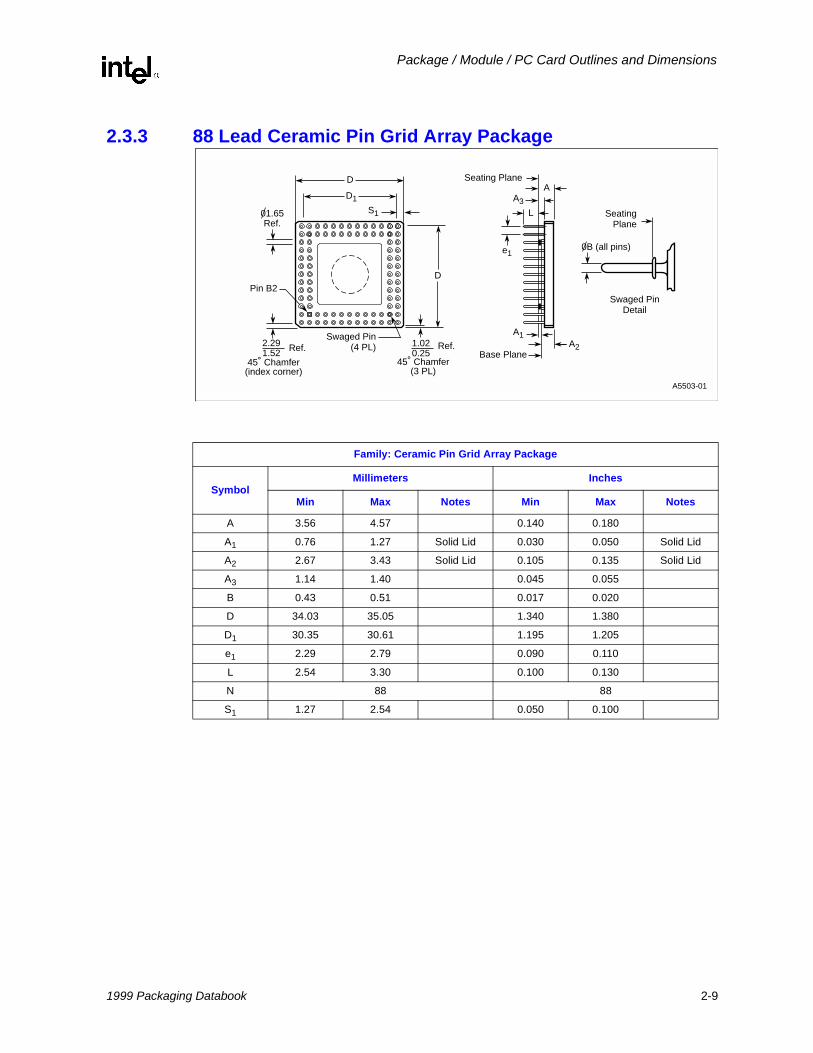
2.3.3 88 Lead Ceramic Pin Grid Array Package
A5503-01
D
A3
1.020.25
D
D1
Swaged Pin(4 PL)
Base PlaneA2
A1
e1
A
S1
Ref.
45˚ Chamfer(3 PL)
2.291.52
45˚ Chamfer(index corner)
Ref.
01.65Ref.
Pin B2
L
Seating Plane
SeatingPlane
Swaged PinDetail
0B (all pins)
Family: Ceramic Pin Grid Array Package
SymbolMillimeters Inches
Min Max Notes Min Max Notes
A 3.56 4.57 0.140 0.180
A1 0.76 1.27 Solid Lid 0.030 0.050 Solid Lid
A2 2.67 3.43 Solid Lid 0.105 0.135 Solid Lid
A3 1.14 1.40 0.045 0.055
B 0.43 0.51 0.017 0.020
D 34.03 35.05 1.340 1.380
D1 30.35 30.61 1.195 1.205
e1 2.29 2.79 0.090 0.110
L 2.54 3.30 0.100 0.130
N 88 88
S1 1.27 2.54 0.050 0.100
1999 Packaging Databook 2-9
Package / Module / PC Card Outlines and Dimensions
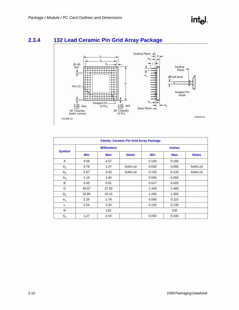
2.3.4 132 Lead Ceramic Pin Grid Array Package
A5504-01
D
A3
1.020.25
Swaged Pin(4 PL)
Base PlaneA2
A1
e1
A
S1
Ref.
45˚ Chamfer(3 PL)
2.291.52
45˚ Chamfer(index corner)
Ref.
01.65Ref.
Pin C3
L
Seating Plane
SeatingPlane
Swaged PinDetail
0B (all pins)
DD1
231369-16
Family: Ceramic Pin Grid Array Package
SymbolMillimeters Inches
Min Max Notes Min Max Notes
A 3.56 4.57 0.140 0.180
A1 0.76 1.27 Solid Lid 0.030 0.050 Solid Lid
A2 2.67 3.43 Solid Lid 0.105 0.135 Solid Lid
A3 1.14 1.40 0.045 0.055
B 0.43 0.51 0.017 0.020
D 36.57 37.59 1.440 1.480
D1 32.89 33.15 1.295 1.305
e1 2.29 2.79 0.090 0.110
L 2.54 3.30 0.100 0.130
N 132 132
S1 1.27 2.54 0.050 0.100
2-10 1999 Packaging Databook
Package / Module / PC Card Outlines and Dimensions
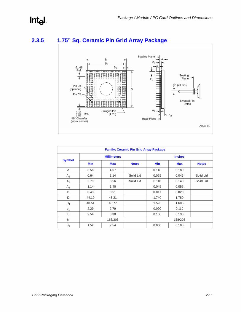
2.3.5 1.75” Sq. Ceramic Pin Grid Array Package
A5505-01
D
A3DD1
Swaged Pin(4 PL)
Base PlaneA2
A1
e1
A
S1
2.291.52
45˚ Chamfer(index corner)
Ref.
01.65Ref.
L
Seating Plane
SeatingPlane
Swaged PinDetail
0B (all pins)
Pin C3
Pin D4(optional)
Family: Ceramic Pin Grid Array Package
SymbolMillimeters Inches
Min Max Notes Min Max Notes
A 3.56 4.57 0.140 0.180
A1 0.64 1.14 Solid Lid 0.025 0.045 Solid Lid
A2 2.79 3.56 Solid Lid 0.110 0.140 Solid Lid
A3 1.14 1.40 0.045 0.055
B 0.43 0.51 0.017 0.020
D 44.19 45.21 1.740 1.780
D1 40.51 40.77 1.595 1.605
e1 2.29 2.79 0.090 0.110
L 2.54 3.30 0.100 0.130
N 168/208 168/208
S1 1.52 2.54 0.060 0.100
1999 Packaging Databook 2-11

Package / Module / PC Card Outlines and Dimensions
2.3.6 1.95” Sq. Ceramic Pin Grid Array Package
A5506-01
D
A3
DD1
Base PlaneA2
A1
e1
A
S1
2.291.52
45˚ Chamfer(index corner)
Ref.
01.65Ref.
L
Seating Plane
SeatingPlane
Swaged PinDetail
0B (all pins)
Swaged Pin(4 PL)
Pin D4
Pin E5(optional)
231369-19
Family: Ceramic Pin Grid Array Package
SymbolMillimeters Inches
Min Max Notes Min Max Notes
A 3.56 4.57 0.140 0.180
A1 0.64 1.14 Ceramic Lid 0.025 0.045 Ceramic
A2 2.79 3.56 Ceramic Lid 0.110 0.140 Ceramic
A3 1.14 1.40 0.045 0.055
B 0.43 0.51 0.017 0.020
D 49.27 50.29 1.940 1.980
D1 45.59 45.85 1.795 1.805
e1 2.29 2.79 0.090 0.110
L 2.54 3.30 0.100 0.130
N 240 280 240 280
S1 1.52 2.54 0.060 0.100
2-12 1999 Packaging Databook
Package / Module / PC Card Outlines and Dimensions
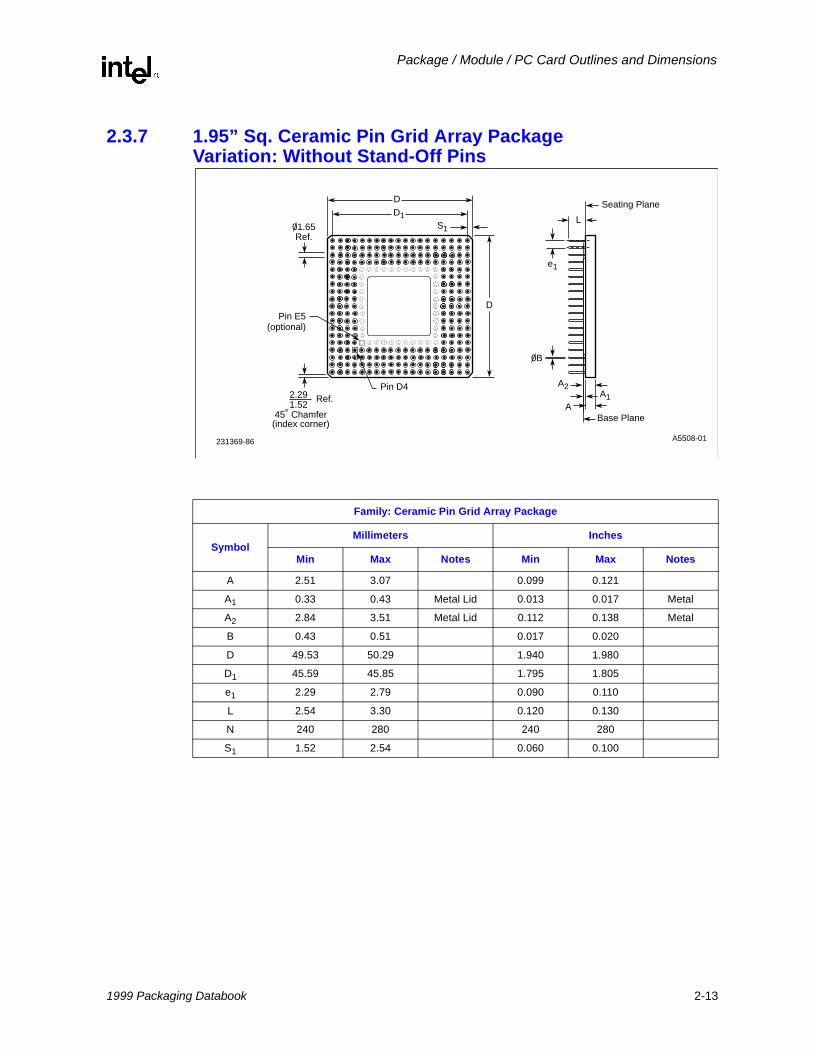
2.3.7 1.95” Sq. Ceramic Pin Grid Array Package Variation: Without Stand-Off Pins
A5508-01
D
DD1
Base Plane
A2A1
0B
e1
S1
2.291.52
45˚ Chamfer(index corner)
Ref.
01.65Ref.
L
Seating Plane
Pin E5(optional)
Pin D4
A
231369-86
Family: Ceramic Pin Grid Array Package
SymbolMillimeters Inches
Min Max Notes Min Max Notes
A 2.51 3.07 0.099 0.121
A1 0.33 0.43 Metal Lid 0.013 0.017 Metal
A2 2.84 3.51 Metal Lid 0.112 0.138 Metal
B 0.43 0.51 0.017 0.020
D 49.53 50.29 1.940 1.980
D1 45.59 45.85 1.795 1.805
e1 2.29 2.79 0.090 0.110
L 2.54 3.30 0.120 0.130
N 240 280 240 280
S1 1.52 2.54 0.060 0.100
1999 Packaging Databook 2-13

Package / Module / PC Card Outlines and Dimensions
2.3.8 2.16” Sq. Ceramic Pin Grid Array Package Variation: Without Stand-Off Pins
A5510-01
D
DD1
Base Plane
A2
0B
S1
2.291.52
45˚ Chamfer(index corner)
Ref.
01.65Ref.
L
Seating Plane
Pin D4
A
e1
A1
231369-91
Family: Ceramic Pin Grid Array Package
SymbolMillimeters Inches
Min Max Notes Min Max Notes
A 2.62 2.97 0.103 0.117
A1 0.38 0.43 Metal Lid 0.015 0.017 Metal Lid
A2 2.94 3.48 Metal Lid 0.116 0.137 Metal Lid
B 0.43 0.51 0.017 0.020
D 54.61 55.12 2.150 2.170
D1 50.67 50.93 1.995 2.005
e1 2.29 2.79 0.090 0.110
L 2.54 3.30 0.120 0.130
N 272 320 272 320
S1 1.651 2.16 0.065 0.085
2-14 1999 Packaging Databook
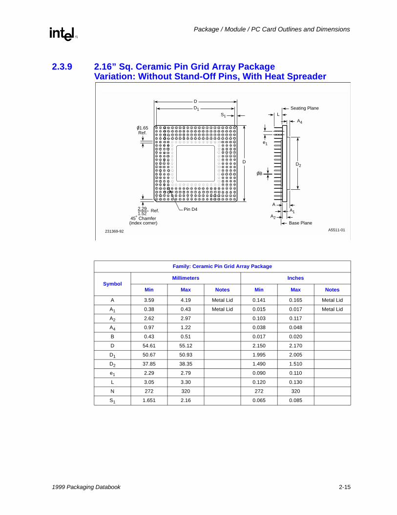
Package / Module / PC Card Outlines and Dimensions
2.3.9 2.16” Sq. Ceramic Pin Grid Array Package Variation: Without Stand-Off Pins, With Heat Spreader
A5511-01
D
DD1
Base Plane
A
0B
S1
2.291.52
45˚ Chamfer(index corner)
Ref.
01.65Ref.
LSeating Plane
Pin D4
A2
e1
A1
D2
A4
231369-92
Family: Ceramic Pin Grid Array Package
SymbolMillimeters Inches
Min Max Notes Min Max Notes
A 3.59 4.19 Metal Lid 0.141 0.165 Metal Lid
A1 0.38 0.43 Metal Lid 0.015 0.017 Metal Lid
A2 2.62 2.97 0.103 0.117
A4 0.97 1.22 0.038 0.048
B 0.43 0.51 0.017 0.020
D 54.61 55.12 2.150 2.170
D1 50.67 50.93 1.995 2.005
D2 37.85 38.35 1.490 1.510
e1 2.29 2.79 0.090 0.110
L 3.05 3.30 0.120 0.130
N 272 320 272 320
S1 1.651 2.16 0.065 0.085
1999 Packaging Databook 2-15
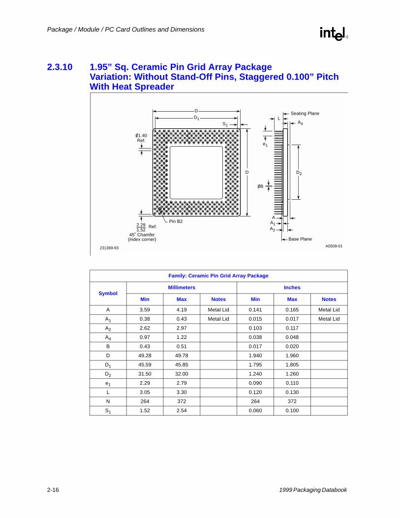
Package / Module / PC Card Outlines and Dimensions
2.3.10 1.95” Sq. Ceramic Pin Grid Array Package Variation: Without Stand-Off Pins, Staggered 0.100” Pitch With Heat Spreader
A5509-01
D
DD1
Base Plane
A1A2
0B
e1
S1
2.291.52
45˚ Chamfer(index corner)
Ref.
01.40Ref.
LSeating Plane
Pin B2A
D2
A4
231369-93
Family: Ceramic Pin Grid Array Package
SymbolMillimeters Inches
Min Max Notes Min Max Notes
A 3.59 4.19 Metal Lid 0.141 0.165 Metal Lid
A1 0.38 0.43 Metal Lid 0.015 0.017 Metal Lid
A2 2.62 2.97 0.103 0.117
A4 0.97 1.22 0.038 0.048
B 0.43 0.51 0.017 0.020
D 49.28 49.78 1.940 1.960
D1 45.59 45.85 1.795 1.805
D2 31.50 32.00 1.240 1.260
e1 2.29 2.79 0.090 0.110
L 3.05 3.30 0.120 0.130
N 264 372 264 372
S1 1.52 2.54 0.060 0.100
2-16 1999 Packaging Databook
Package / Module / PC Card Outlines and Dimensions
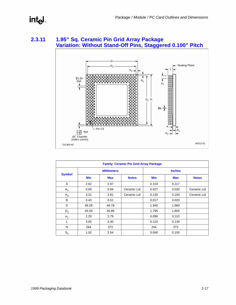
2.3.11 1.95” Sq. Ceramic Pin Grid Array Package Variation: Without Stand-Off Pins, Staggered 0.100” Pitch
A5512-01
D
D
D1
A1A2
0B
e1
S1
2.291.52
45˚ Chamfer(index corner)
Ref.
01.65Ref.
LSeating Plane
Pin C3A
S1
D1
231369-A0
Family: Ceramic Pin Grid Array Package
SymbolMillimeters Inches
Min Max Notes Min Max Notes
A 2.62 2.97 0.103 0.117
A1 0.69 0.84 Ceramic Lid 0.027 0.033 Ceramic Lid
A2 3.31 3.81 Ceramic Lid 0.130 0.150 Ceramic Lid
B 0.43 0.51 0.017 0.020
D 49.28 49.78 1.940 1.960
D1 45.59 45.85 1.795 1.805
e1 2.29 2.79 0.090 0.110
L 3.05 3.30 0.120 0.130
N 264 372 264 372
S1 1.52 2.54 0.060 0.100
1999 Packaging Databook 2-17
Package / Module / PC Card Outlines and Dimensions
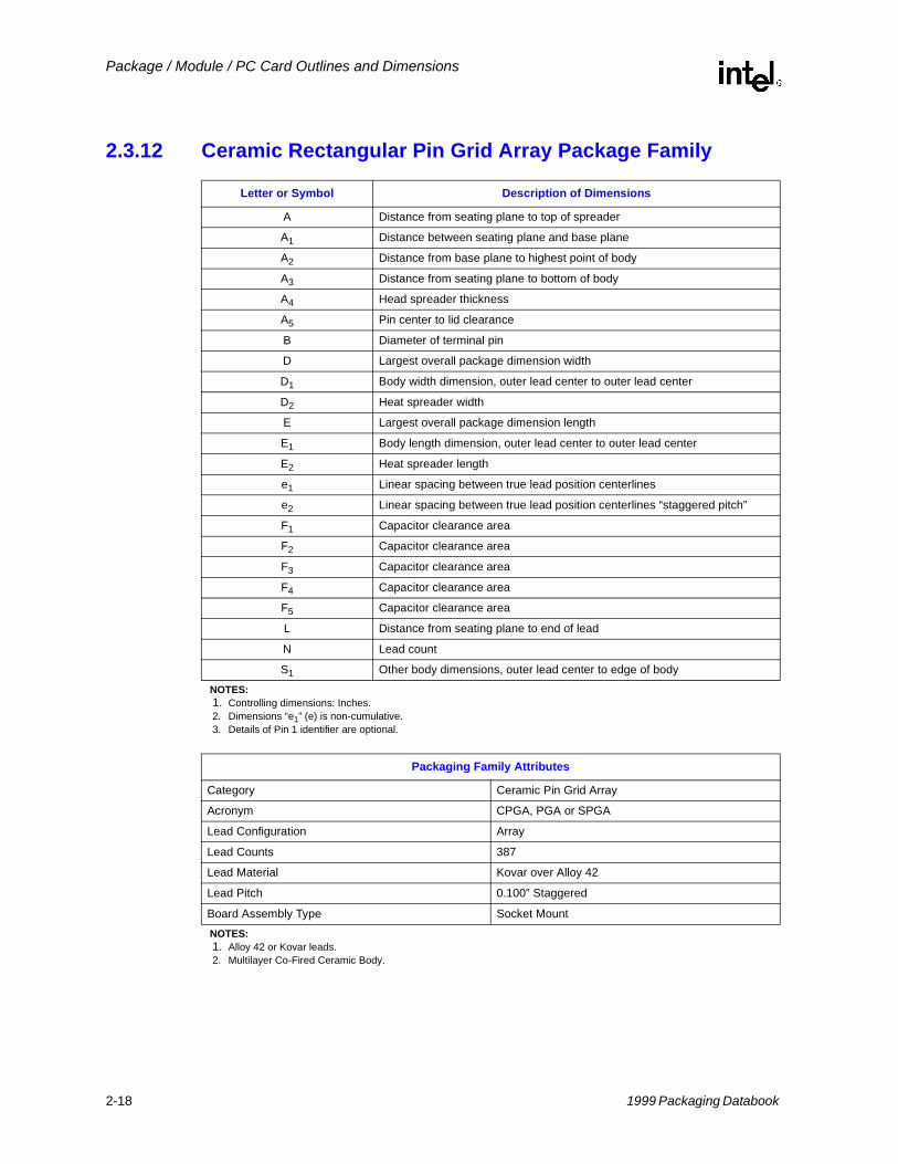
2.3.12 Ceramic Rectangular Pin Grid Array Package Family
Letter or Symbol Description of Dimensions
A Distance from seating plane to top of spreader
A1 Distance between seating plane and base plane
A2 Distance from base plane to highest point of body
A3 Distance from seating plane to bottom of body
A4 Head spreader thickness
A5 Pin center to lid clearance
B Diameter of terminal pin
D Largest overall package dimension width
D1 Body width dimension, outer lead center to outer lead center
D2 Heat spreader width
E Largest overall package dimension length
E1 Body length dimension, outer lead center to outer lead center
E2 Heat spreader length
e1 Linear spacing between true lead position centerlines
e2 Linear spacing between true lead position centerlines “staggered pitch”
F1 Capacitor clearance area
F2 Capacitor clearance area
F3 Capacitor clearance area
F4 Capacitor clearance area
F5 Capacitor clearance area
L Distance from seating plane to end of lead
N Lead count
S1 Other body dimensions, outer lead center to edge of bodyNOTES: 1. Controlling dimensions: Inches.2. Dimensions “e1” (e) is non-cumulative.3. Details of Pin 1 identifier are optional.
Packaging Family Attributes
Category Ceramic Pin Grid Array
Acronym CPGA, PGA or SPGA
Lead Configuration Array
Lead Counts 387
Lead Material Kovar over Alloy 42
Lead Pitch 0.100” Staggered
Board Assembly Type Socket MountNOTES: 1. Alloy 42 or Kovar leads.2. Multilayer Co-Fired Ceramic Body.
2-18 1999 Packaging Databook
Package / Module / PC Card Outlines and Dimensions
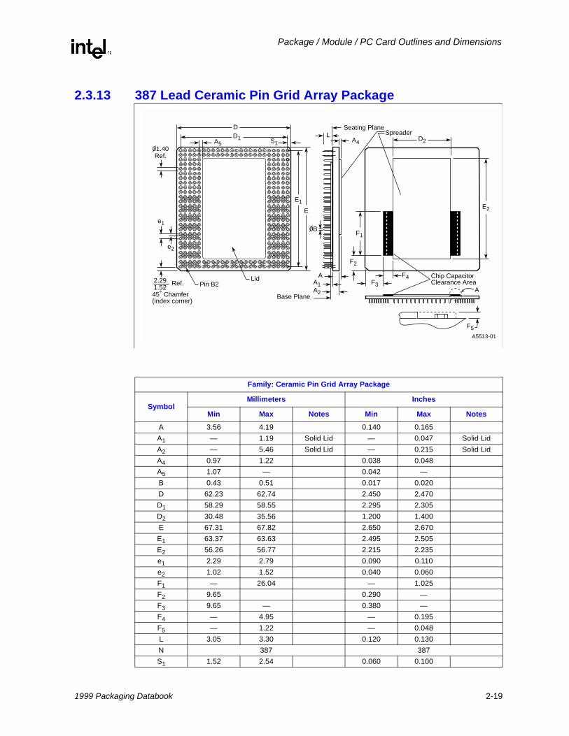
2.3.13 387 Lead Ceramic Pin Grid Array Package
A5513-01
E
DD1
Base Plane
A
0B
S1
2.291.5245˚ Chamfer(index corner)
Ref.
01.40Ref.
LSeating Plane
Lid
A2
e1
A1
A4A5
E1
e2
E2
D2
F1
F2
F3
F4
Spreader
Chip CapacitorClearance Area
A
F5
Pin B2
Family: Ceramic Pin Grid Array Package
SymbolMillimeters Inches
Min Max Notes Min Max NotesA 3.56 4.19 0.140 0.165A1 — 1.19 Solid Lid — 0.047 Solid LidA2 — 5.46 Solid Lid — 0.215 Solid LidA4 0.97 1.22 0.038 0.048A5 1.07 — 0.042 —B 0.43 0.51 0.017 0.020D 62.23 62.74 2.450 2.470D1 58.29 58.55 2.295 2.305D2 30.48 35.56 1.200 1.400E 67.31 67.82 2.650 2.670E1 63.37 63.63 2.495 2.505E2 56.26 56.77 2.215 2.235e1 2.29 2.79 0.090 0.110e2 1.02 1.52 0.040 0.060F1 — 26.04 — 1.025F2 9.65 0.290 —F3 9.65 — 0.380 —F4 — 4.95 — 0.195F5 — 1.22 — 0.048L 3.05 3.30 0.120 0.130N 387 387S1 1.52 2.54 0.060 0.100
1999 Packaging Databook 2-19
Package / Module / PC Card Outlines and Dimensions
2.4 Cerdip Dual In-line Package
2.4.1 Symbol List for Cerdip Dual In-Line Family
Letter or Symbol Description of Dimensions
A Distance from seating plane to highest point of body
A1 Distance between seating plane and base plane
A2 Distance from base plane to highest point of body (lid)
A3 Base body thickness
B Width of terminal leads
B1 Width of terminal lead shoulder which locate seating plane (standoff geometry optional)
C Thickness of terminal leads
D Largest overall package dimension of length
D2 A body length dimension, end lead center to end lead center
E Largest overall package width dimension outside of lead
E1 Body width dimensions not including leads
eA Linear spacing of true minimum lead position center line to center line
eB Linear spacing between true lead position outside of lead to outside of lead
e1 Linear spacing between centerlines of body standoffs (terminal leads)
L Distance from seating plane to end of lead
N The total number of potentially usable lead positions
S Distance from true position centerline of No. 1 lead position to the extremity of the body
S1 Distance from outer end lead edge positions to the extremity of the body
α Angular spacing between minimum and maximum lead positions measured at the gauge planeNOTES: 1. Controlling dimension: millimeter.2. Dimension “e1” (“e”) is non-cumulative.3. Seating plane (standoff) is defined by P.C. board hole size: 0.0415 - 0.0430 inch.4. Dimension “B1” is normal.
Package Family Attributes
Category Cerdip
Acronym Cerdip
Lead Configuration Dual-In-Line
Lead Counts 20, 28, 40
Lead Finish Hot Solder Dip
Lead Pitch 0.100”
Board Assembly Type Socket and Surface MountNOTES: 1. Alloy 42 Leads.2. Pressed Ceramic Body.3. UV Window is available for reprogramming.
2-20 1999 Packaging Databook
Package / Module / PC Card Outlines and Dimensions
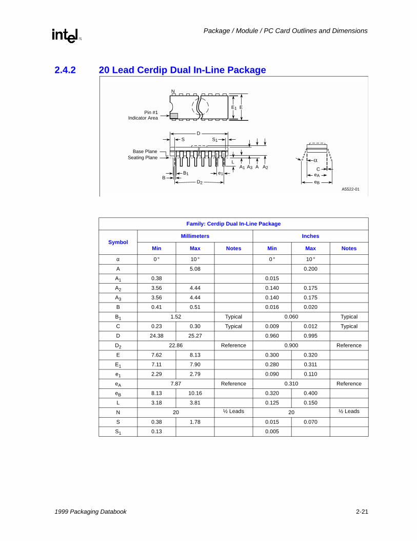
2.4.2 20 Lead Cerdip Dual In-Line Package
A5522-01
N
e1B
B1
D2
DS S1
Seating PlaneBase Plane
LA1 A2A3 A
eB
eA
C
EE1Pin #1
Indicator Area
Family: Cerdip Dual In-Line Package
SymbolMillimeters Inches
Min Max Notes Min Max Notes
α 0 ° 10 ° 0 ° 10 °
A 5.08 0.200
A1 0.38 0.015
A2 3.56 4.44 0.140 0.175
A3 3.56 4.44 0.140 0.175
B 0.41 0.51 0.016 0.020
B1 1.52 Typical 0.060 Typical
C 0.23 0.30 Typical 0.009 0.012 Typical
D 24.38 25.27 0.960 0.995
D2 22.86 Reference 0.900 Reference
E 7.62 8.13 0.300 0.320
E1 7.11 7.90 0.280 0.311
e1 2.29 2.79 0.090 0.110
eA 7.87 Reference 0.310 Reference
eB 8.13 10.16 0.320 0.400
L 3.18 3.81 0.125 0.150
N 20 ½ Leads 20 ½ Leads
S 0.38 1.78 0.015 0.070
S1 0.13 0.005
1999 Packaging Databook 2-21
Package / Module / PC Card Outlines and Dimensions
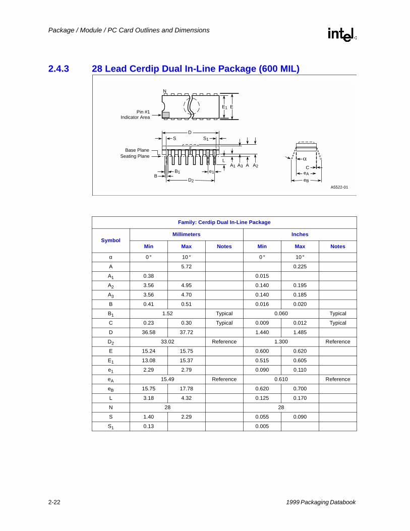
2.4.3 28 Lead Cerdip Dual In-Line Package (600 MIL)
A5522-01
N
e1B
B1
D2
DS S1
Seating PlaneBase Plane
LA1 A2A3 A
eB
eA
C
EE1Pin #1
Indicator Area
Family: Cerdip Dual In-Line Package
SymbolMillimeters Inches
Min Max Notes Min Max Notes
α 0 ° 10 ° 0 ° 10 °
A 5.72 0.225
A1 0.38 0.015
A2 3.56 4.95 0.140 0.195
A3 3.56 4.70 0.140 0.185
B 0.41 0.51 0.016 0.020
B1 1.52 Typical 0.060 Typical
C 0.23 0.30 Typical 0.009 0.012 Typical
D 36.58 37.72 1.440 1.485
D2 33.02 Reference 1.300 Reference
E 15.24 15.75 0.600 0.620
E1 13.08 15.37 0.515 0.605
e1 2.29 2.79 0.090 0.110
eA 15.49 Reference 0.610 Reference
eB 15.75 17.78 0.620 0.700
L 3.18 4.32 0.125 0.170
N 28 28
S 1.40 2.29 0.055 0.090
S1 0.13 0.005
2-22 1999 Packaging Databook
Package / Module / PC Card Outlines and Dimensions
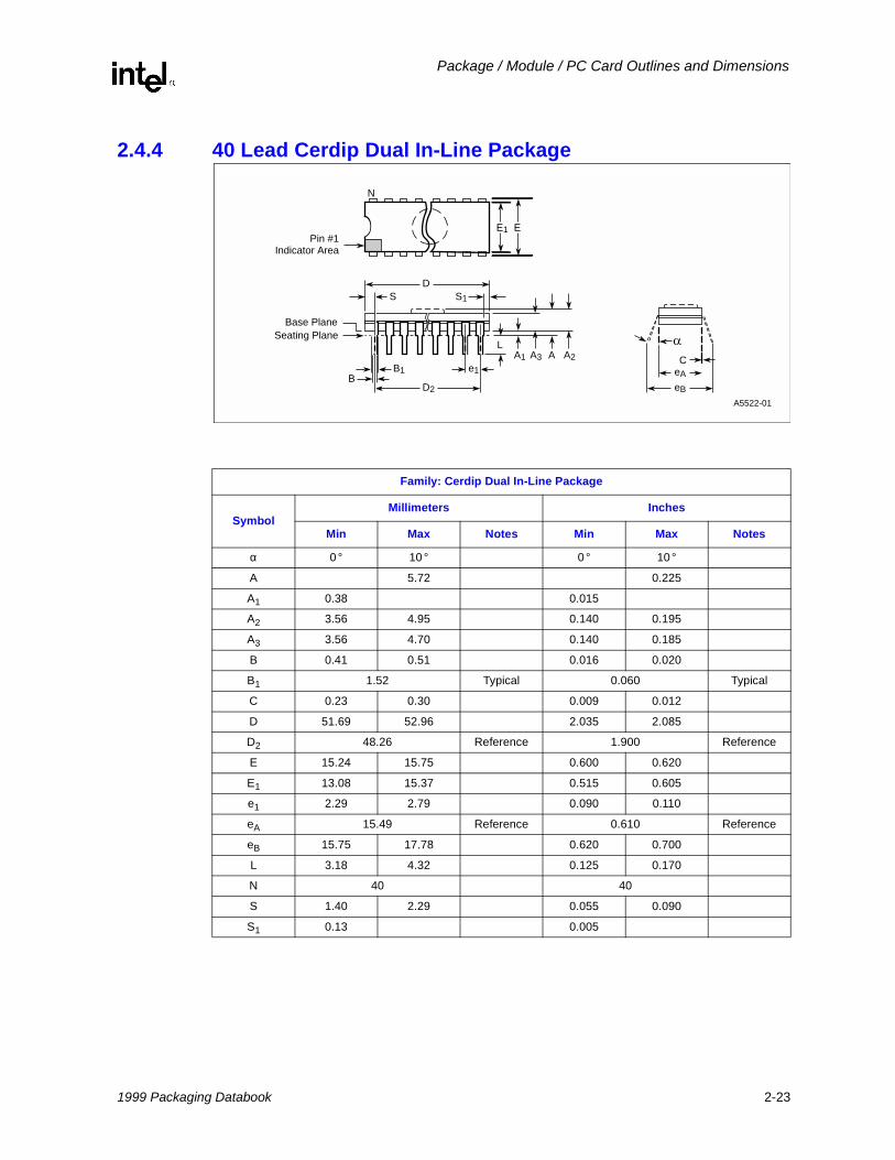
2.4.4 40 Lead Cerdip Dual In-Line Package
A5522-01
N
e1B
B1
D2
DS S1
Seating PlaneBase Plane
LA1 A2A3 A
eB
eA
C
EE1Pin #1
Indicator Area
Family: Cerdip Dual In-Line Package
SymbolMillimeters Inches
Min Max Notes Min Max Notes
α 0 ° 10 ° 0 ° 10 °
A 5.72 0.225
A1 0.38 0.015
A2 3.56 4.95 0.140 0.195
A3 3.56 4.70 0.140 0.185
B 0.41 0.51 0.016 0.020
B1 1.52 Typical 0.060 Typical
C 0.23 0.30 0.009 0.012
D 51.69 52.96 2.035 2.085
D2 48.26 Reference 1.900 Reference
E 15.24 15.75 0.600 0.620
E1 13.08 15.37 0.515 0.605
e1 2.29 2.79 0.090 0.110
eA 15.49 Reference 0.610 Reference
eB 15.75 17.78 0.620 0.700
L 3.18 4.32 0.125 0.170
N 40 40
S 1.40 2.29 0.055 0.090
S1 0.13 0.005
1999 Packaging Databook 2-23
Package / Module / PC Card Outlines and Dimensions
2.5 Plastic Dual In-line Package
2.5.1 Symbol List for Plastic Dual In-Line Family
Letter or Symbol Description of Dimensions
α Angular spacing between minimum and maximum lead positions measured at the gauge plane
A Distance from seating plane to highest point of body (lid)
A1 Distance between seating plane and base plane
A2 Distance from base plane to highest point of body (lid)
A3 Base body thickness
B Width of terminal leads
B1 Width of terminal lead shoulder which locates seating plane (standoff geometry optional)
C Thickness of terminal leads
D Largest overall package dimension of length
D2 A body length dimension, end lead center to end lead center
E Largest overall package width dimension outside of lead
E1 Body width dimensions not including leads
eA Linear spacing of true minimum lead position center line to center line
eB Linear spacing between true lead position outside of lead to outside of lead
e1 Linear spacing between centerlines of body standoffs (terminal leads)
L Distance from seating plane to end of lead
N The total number of potentially usable lead positions
S Distance from true position centerline of No. 1 lead position to the extremity of the body
S1 Distance from outer end lead edge positions to the extremity of the bodyNOTES: 1. Controlling dimension: millimeter.2. Dimension “e1” (“e”) is non-cumulative.3. Seating plane (standoff) is defined by P.C. board hole size: 0.0415 - 0.0430 inch.4. Dimension “B1” is normal.5. Details of Pin 1 identifier are optional.
Packaging Family Attributes
Category Plastic Dual-In-Line
Acronym PDIP
Lead Configuration Dual-In-Line
Lead Counts 24, 28, 32, 40, 64
Lead Finish Solder Coat
Lead Pitch 0.100” (excludes shrink)
Board Assembly Type Socket and Surface MountNOTES: 1. Alloy 42 and Cu Alloy Leads
2-24 1999 Packaging Databook
Package / Module / PC Card Outlines and Dimensions
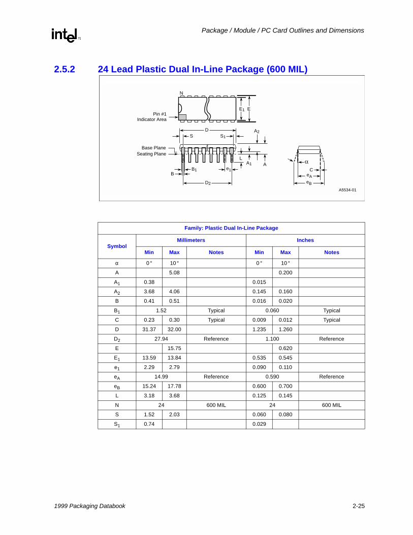
2.5.2 24 Lead Plastic Dual In-Line Package (600 MIL)
A5534-01
N
e1B
B1
D2
DS S1
Seating PlaneBase Plane
LA1
A2
A
EE1Pin #1
Indicator Area
eB
eA
C
Family: Plastic Dual In-Line Package
SymbolMillimeters Inches
Min Max Notes Min Max Notes
α 0 ° 10 ° 0 ° 10 °
A 5.08 0.200
A1 0.38 0.015
A2 3.68 4.06 0.145 0.160
B 0.41 0.51 0.016 0.020
B1 1.52 Typical 0.060 Typical
C 0.23 0.30 Typical 0.009 0.012 Typical
D 31.37 32.00 1.235 1.260
D2 27.94 Reference 1.100 Reference
E 15.75 0.620
E1 13.59 13.84 0.535 0.545
e1 2.29 2.79 0.090 0.110
eA 14.99 Reference 0.590 Reference
eB 15.24 17.78 0.600 0.700
L 3.18 3.68 0.125 0.145
N 24 600 MIL 24 600 MIL
S 1.52 2.03 0.060 0.080
S1 0.74 0.029
1999 Packaging Databook 2-25
Package / Module / PC Card Outlines and Dimensions
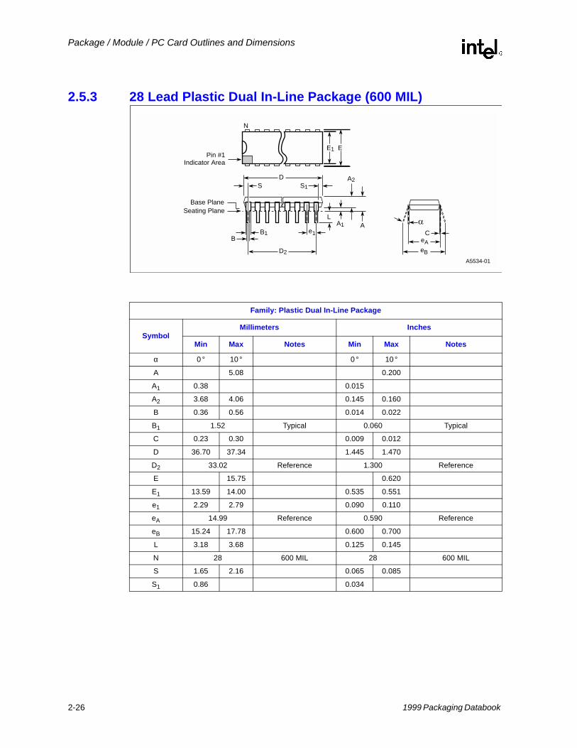
2.5.3 28 Lead Plastic Dual In-Line Package (600 MIL)
A5534-01
N
e1B
B1
D2
DS S1
Seating PlaneBase Plane
LA1
A2
A
EE1Pin #1
Indicator Area
eB
eA
C
Family: Plastic Dual In-Line Package
SymbolMillimeters Inches
Min Max Notes Min Max Notes
α 0 ° 10 ° 0 ° 10 °
A 5.08 0.200
A1 0.38 0.015
A2 3.68 4.06 0.145 0.160
B 0.36 0.56 0.014 0.022
B1 1.52 Typical 0.060 Typical
C 0.23 0.30 0.009 0.012
D 36.70 37.34 1.445 1.470
D2 33.02 Reference 1.300 Reference
E 15.75 0.620
E1 13.59 14.00 0.535 0.551
e1 2.29 2.79 0.090 0.110
eA 14.99 Reference 0.590 Reference
eB 15.24 17.78 0.600 0.700
L 3.18 3.68 0.125 0.145
N 28 600 MIL 28 600 MIL
S 1.65 2.16 0.065 0.085
S1 0.86 0.034
2-26 1999 Packaging Databook
Package / Module / PC Card Outlines and Dimensions
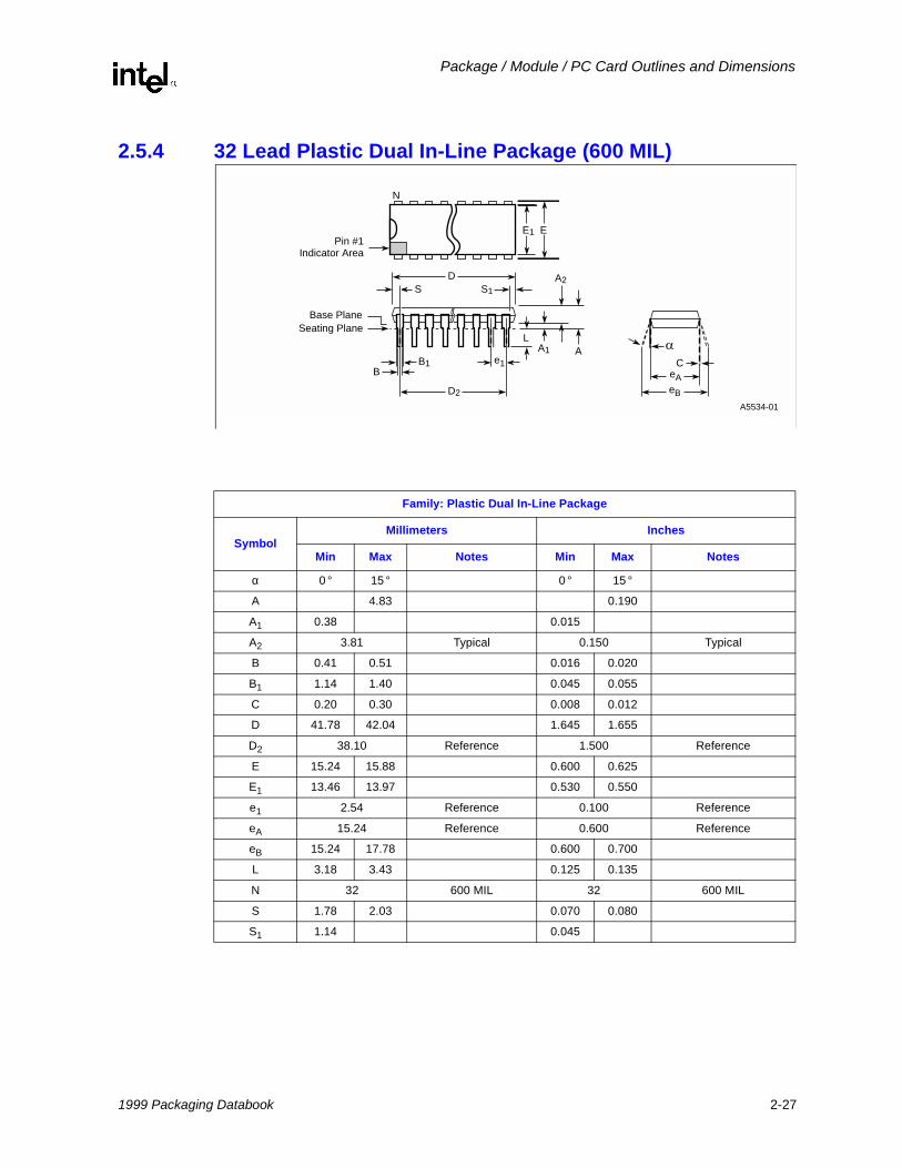
2.5.4 32 Lead Plastic Dual In-Line Package (600 MIL)
A5534-01
N
e1B
B1
D2
DS S1
Seating PlaneBase Plane
LA1
A2
A
EE1Pin #1
Indicator Area
eB
eA
C
Family: Plastic Dual In-Line Package
SymbolMillimeters Inches
Min Max Notes Min Max Notes
α 0 ° 15 ° 0 ° 15 °
A 4.83 0.190
A1 0.38 0.015
A2 3.81 Typical 0.150 Typical
B 0.41 0.51 0.016 0.020
B1 1.14 1.40 0.045 0.055
C 0.20 0.30 0.008 0.012
D 41.78 42.04 1.645 1.655
D2 38.10 Reference 1.500 Reference
E 15.24 15.88 0.600 0.625
E1 13.46 13.97 0.530 0.550
e1 2.54 Reference 0.100 Reference
eA 15.24 Reference 0.600 Reference
eB 15.24 17.78 0.600 0.700
L 3.18 3.43 0.125 0.135
N 32 600 MIL 32 600 MIL
S 1.78 2.03 0.070 0.080
S1 1.14 0.045
1999 Packaging Databook 2-27

Package / Module / PC Card Outlines and Dimensions
2.5.5 40 Lead Plastic Dual In-Line Package (600 MIL)
A5534-01
N
e1B
B1
D2
DS S1
Seating PlaneBase Plane
LA1
A2
A
EE1Pin #1
Indicator Area
eB
eA
C
Family: Plastic Dual In-Line Package
SymbolMillimeters Inches
Min Max Notes Min Max Notes
α 0 ° 10 ° 0 ° 10 °
A 5.08 0.200
A1 0.38 0.015
A2 3.94 4.19 0.155 0.165
B 0.41 0.51 0.016 0.020
B1 1.27 Typical 0.050 Typical
C 0.23 0.30 0.009 0.012
D 51.94 52.58 2.045 2.070
D2 48.26 Reference 1.900 Reference
E 15.75 0.620
E1 13.59 13.84 0.535 0.545
e1 2.29 2.79 0.090 0.110
eA 14.99 Reference 0.590 Reference
eB 15.24 17.78 0.600 0.700
L 3.18 3.68 0.125 0.145
N 40 40
S 1.65 2.16 0.065 0.085
S1 0.99 0.039
2-28 1999 Packaging Databook
Package / Module / PC Card Outlines and Dimensions
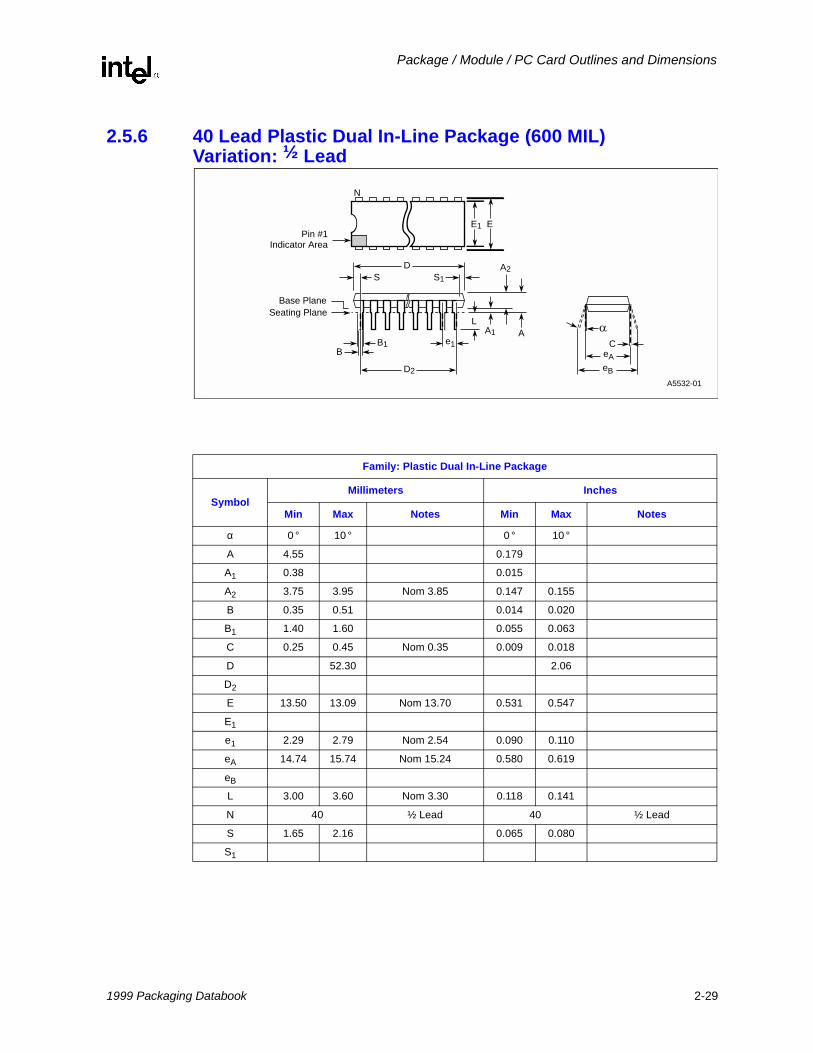
2.5.6 40 Lead Plastic Dual In-Line Package (600 MIL)Variation: ½ Lead
A5532-01
N
e1B
B1
D2
DS S1
Seating PlaneBase Plane
LA1
A2
A
eB
eA
C
EE1Pin #1
Indicator Area
Family: Plastic Dual In-Line Package
SymbolMillimeters Inches
Min Max Notes Min Max Notes
α 0 ° 10 ° 0 ° 10 °
A 4.55 0.179
A1 0.38 0.015
A2 3.75 3.95 Nom 3.85 0.147 0.155
B 0.35 0.51 0.014 0.020
B1 1.40 1.60 0.055 0.063
C 0.25 0.45 Nom 0.35 0.009 0.018
D 52.30 2.06
D2
E 13.50 13.09 Nom 13.70 0.531 0.547
E1
e1 2.29 2.79 Nom 2.54 0.090 0.110
eA 14.74 15.74 Nom 15.24 0.580 0.619
eB
L 3.00 3.60 Nom 3.30 0.118 0.141
N 40 ½ Lead 40 ½ Lead
S 1.65 2.16 0.065 0.080
S1
1999 Packaging Databook 2-29
Package / Module / PC Card Outlines and Dimensions
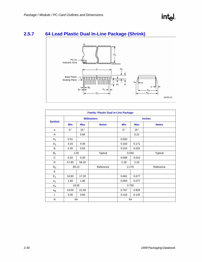
2.5.7 64 Lead Plastic Dual In-Line Package (Shrink)
A5533-01
N
e1BB1
D2
D
Seating PlaneBase Plane
LA1
A2
A
eB
eA
C
E1
Pin #1Indicator Area
Family: Plastic Dual In-Line Package
SymbolMillimeters Inches
Min Max Notes Min Max Notes
α 0 ° 15 ° 0 ° 15 °
A 5.65 0.22
A1 0.51 0.020
A2 4.15 4.35 0.163 0.171
B 0.35 0.55 0.014 0.022
B1 1.00 Typical 0.040 Typical
C 0.20 0.30 0.008 0.012
D 57.80 58.20 2.28 2.29
D2 55.12 Reference 2.170 Reference
E
E1 16.80 17.20 0.661 0.677
e1 1.60 1.96 0.063 0.077
eA 19.05 0.750
eB 19.50 21.00 0.767 0.826
L 3.00 3.60 0.118 0.142
N 64 64
2-30 1999 Packaging Databook
Package / Module / PC Card Outlines and Dimensions
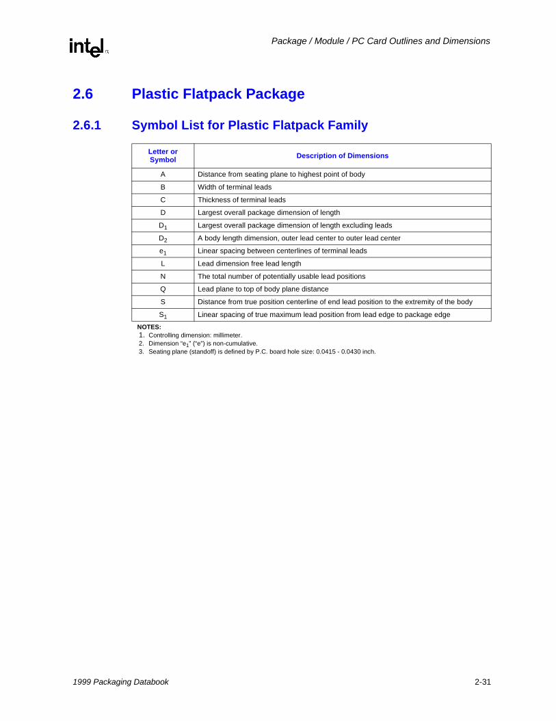
2.6 Plastic Flatpack Package
2.6.1 Symbol List for Plastic Flatpack Family
Letter or Symbol Description of Dimensions
A Distance from seating plane to highest point of body
B Width of terminal leads
C Thickness of terminal leads
D Largest overall package dimension of length
D1 Largest overall package dimension of length excluding leads
D2 A body length dimension, outer lead center to outer lead center
e1 Linear spacing between centerlines of terminal leads
L Lead dimension free lead length
N The total number of potentially usable lead positions
Q Lead plane to top of body plane distance
S Distance from true position centerline of end lead position to the extremity of the body
S1 Linear spacing of true maximum lead position from lead edge to package edgeNOTES: 1. Controlling dimension: millimeter.2. Dimension “e1” (“e”) is non-cumulative.3. Seating plane (standoff) is defined by P.C. board hole size: 0.0415 - 0.0430 inch.
1999 Packaging Databook 2-31
Package / Module / PC Card Outlines and Dimensions
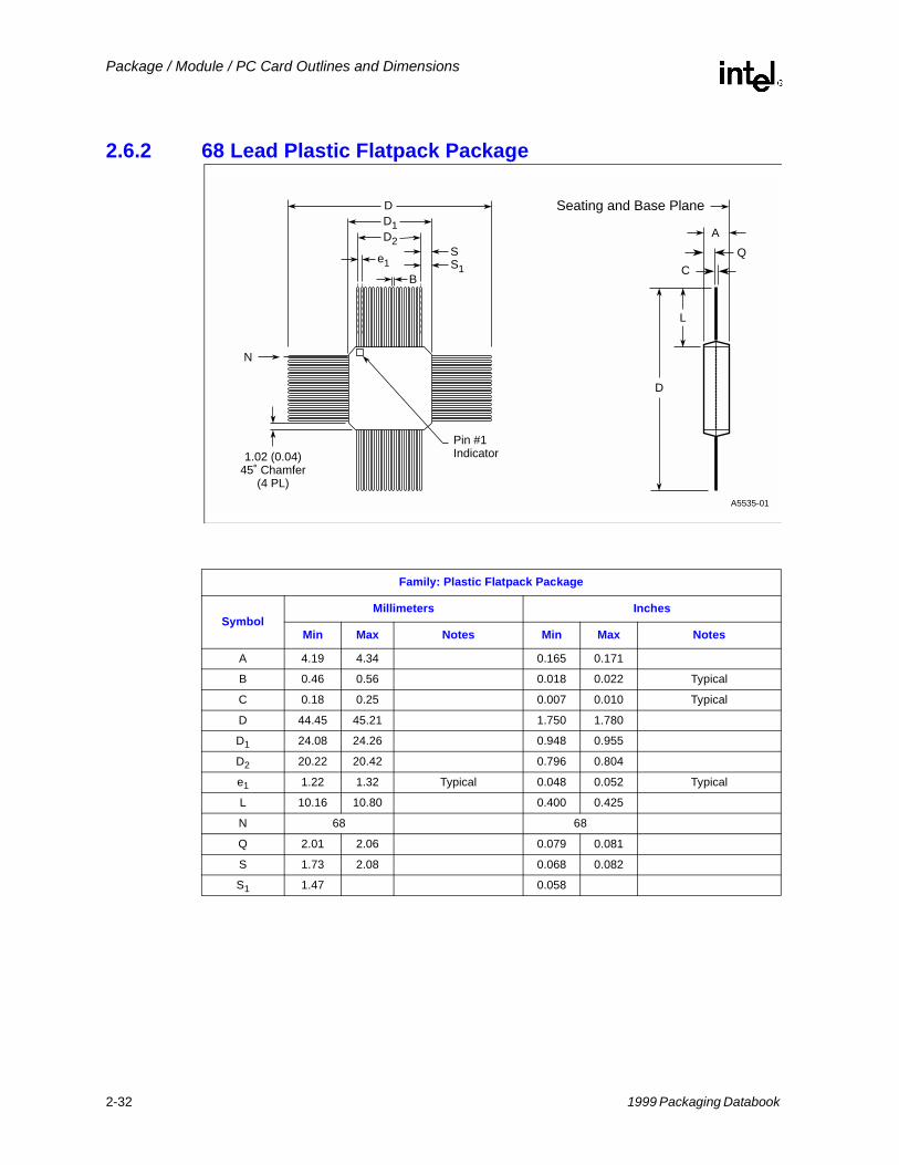
2.6.2 68 Lead Plastic Flatpack Package
A5535-01
D
D2
Seating and Base Plane
e1
L
D
Q
C
D1
N
1.02 (0.04)45˚ Chamfer
(4 PL)
Pin #1Indicator
B
SS1
A
Family: Plastic Flatpack Package
SymbolMillimeters Inches
Min Max Notes Min Max Notes
A 4.19 4.34 0.165 0.171
B 0.46 0.56 0.018 0.022 Typical
C 0.18 0.25 0.007 0.010 Typical
D 44.45 45.21 1.750 1.780
D1 24.08 24.26 0.948 0.955
D2 20.22 20.42 0.796 0.804
e1 1.22 1.32 Typical 0.048 0.052 Typical
L 10.16 10.80 0.400 0.425
N 68 68
Q 2.01 2.06 0.079 0.081
S 1.73 2.08 0.068 0.082
S1 1.47 0.058
2-32 1999 Packaging Databook
Package / Module / PC Card Outlines and Dimensions
2.7 Plastic Leaded Chip Carrier Package
2.7.1 Symbol List for Plastic Leaded Chip Carrier Family
Letter or Symbol Description of Dimensions
A Overall Height: Distance from seating plane to highest point of body
A1 Distance from lead shoulder to seating plane
CP Seating plane coplanarity
D/E Overall package dimension
D1/E1 Plastic body dimension
D2/E2 Footprint
LT Lead thickness
N Total number of potentially usable lead positions
Nd Total number of leads on short side
Ne Total number of leads on long side
TCP Tweezing coplanarityNOTES: RECTANGLE PACKAGE1. All dimensions and tolerances conform to ANSI Y 14.5M-1982.2. Datum plane -H- located at top of mold parting line and coincident with top of lead, where lead exits plastic body.3. Data A-B and -D- to be determined where center leads exit plastic body at datum plane -H-.4. To be determined at seating plane -C-.5. Dimensions D1 and E1 do not include mold protrusion.6. Pin 1 identifier is located within the defined zone.7. These two dimensions determine maximum angle of the lead of certain socket applications. If unit is intended to be
socketed, it is advisable to review these dimensions with the socket supplier.8. Nd denotes the number of leads on the two short sides of the package, one of which contains pin #1. Ne denotes the
number of leads on the two long sides of the package.9. Controlling dimension, inch.10. All dimensions and tolerances include lead trim offset and lead plating finish.11. Tweezing surface planarity is defined as the furthest any lead on a side may be from the datum. The datum is estab-
lished by touching the outermost lead on that side and parallel to A-B or -D-.
Packaging Family Attributes
Category Plastic Leaded Chip Carrier
Acronym PLCC
Lead Configuration Quad
Lead Counts 20, 28, 32, 44, 52, 68, 84
Lead Finish Solder Plate
Lead Pitch 0.050”
Board Assembly Type Socket and Surface MountNOTES: 1. Copper Alloy Leads.2. Novalac Body.3. Bake and desiccant packaging required.
1999 Packaging Databook 2-33

Package / Module / PC Card Outlines and Dimensions
Family: Plastic Lead Chip Carrier-Rectangular (mm)
28 Lead 32 Lead
Symbol Min Max Notes Min Max Notes
A 3.20 3.56 3.20 3.56
A1 1.93 2.29 1.93 2.29
D 9.78 10.0 12.30 12.60
D1 8.81 8.97 11.40 11.50
D2 7.37 8.38 9.91 10.90
E 14.90 15.10 14.90 15.10
E1 13.90 14.00 13.90 14.00
E2 12.40 13.50 12.40 13.50
N 28 32
Nd 5 7
Ne 9 9
CP 0.00 0.10 0.00 0.10
TCP 0.00 0.10 0.00 0.10
LT 0.23 0.38 0.23 0.38
Family: Plastic Lead Chip Carrier-Rectangular (inch)
Symbol28 Lead 32 Lead
Min Max Notes Min Max Notes
A 0.126 0.140 0.126 0.140
A1 0.076 0.090 0.076 0.090
D 0.385 0.394 0.484 0.496
D1 0.347 0.353 0.449 0.453
D2 0.290 0.330 0.390 0.429
E 0.587 0.594 0.587 0.594
E1 0.547 0.551 0.547 0.551
E2 0.488 0.531 0.488 0.531
N 28 32
Nd 5 7
Ne 9 9
CP 0.000 0.004 0.000 0.004
TCP 0.000 0.004 0.000 0.004
LT 0.009 0.015 0.009 0.015
2-34 1999 Packaging Databook

Package / Module / PC Card Outlines and Dimensions
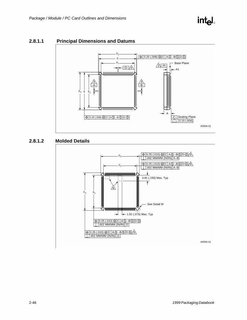
2.7.1.1 Principal Dimensions and Datums
2.7.1.2 Molded Details
A5539-01
A1
D1
3
E1
0.18 (.007) S-BSS A
–C–Seating Plane
Datum Plane2
C
0.18 (.007) S-BSS SDAC
E
–B–3
Ne
–A–3
8
Nd
8
A
–D–
–H–
D
Tweezing Surface
TCP(all four sides)
11
mm (Inch)
A5537-01
BasePlane
0.38 (.015) Min
3 x0.25 (.0101)RNOM
D1
6
3.81 (0.150)Max Typ
.002mm/mm (In/In) D
0.18 (.007) S-BSS A
–C–
Seating Plane
0.74 (.029)0.58 (.023)
x 30˚
1.91 (0.075) Max Typ
5
1.22 (.048)1.07 (.042)
E15
A
.002mm/mm (In/In) A–B
0.18 (.007) S-BSS SDAC
mm (Inch)
1999 Packaging Databook 2-35
Package / Module / PC Card Outlines and Dimensions
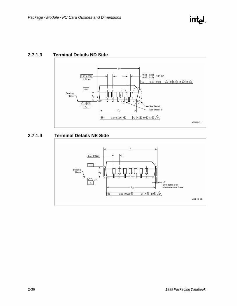
2.7.1.3 Terminal Details ND Side
2.7.1.4 Terminal Details NE Side
A5541-01
0.38 (.015) SDS-BSS AC
0.18 (.007) S-BSS SDAC
4
See Detail L
D
D2
A1
CP–C–
–H–
SeatingPlane
1.27 (.050)0.81 (.032)0.66 (.026) N PLCS
See Detail J
4 Sides
A5540-01
0.38 (.015) S-BSS AC 4
LTSee detail J for Measurement Zone
E
E2
A1
CP–C–
–H–
SeatingPlane
1.27 (.050)
2-36 1999 Packaging Databook
Package / Module / PC Card Outlines and Dimensions
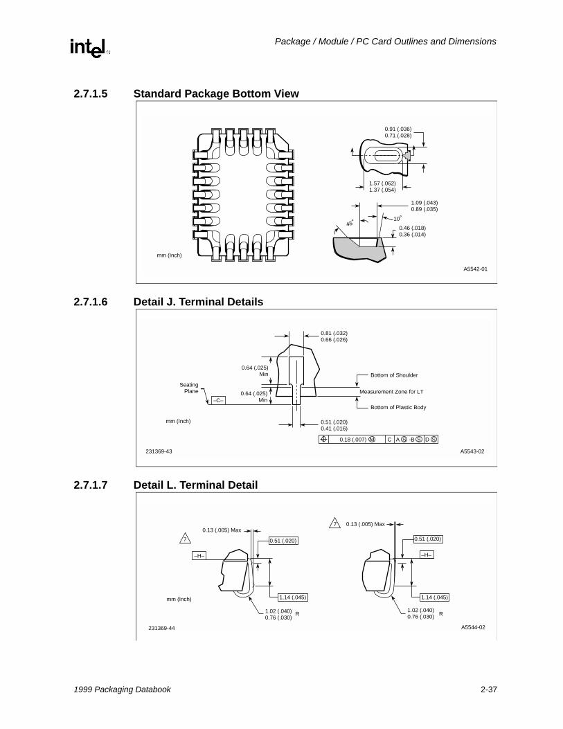
2.7.1.5 Standard Package Bottom View
2.7.1.6 Detail J. Terminal Details
2.7.1.7 Detail L. Terminal Detail
A5542-01
1.57 (.062)1.37 (.054)
0.46 (.018)0.36 (.014)
10˚45˚
0.91 (.036)0.71 (.028)
1.09 (.043)0.89 (.035)
mm (Inch)
A5543-02231369-43
0.18 (.007) SDS-BSM AC
Measurement Zone for LT0.64 (.025)Min
SeatingPlane
0.81 (.032)0.66 (.026)
Bottom of Shoulder
–C–
0.64 (.025)Min
Bottom of Plastic Body
0.51 (.020)0.41 (.016)
mm (Inch)
A5544-02231369-44
1.02 (.040)0.76 (.030)
–H–
0.51 (.020)
1.14 (.045)
0.13 (.005) Max
7
1.02 (.040)0.76 (.030)
–H–
0.51 (.020)
1.14 (.045)
0.13 (.005) Max7
RR
mm (Inch)
1999 Packaging Databook 2-37
Package / Module / PC Card Outlines and Dimensions
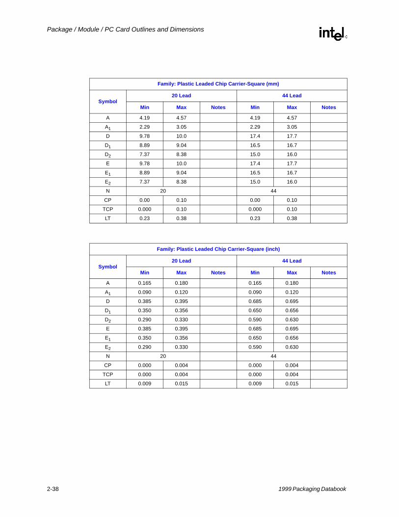
Family: Plastic Leaded Chip Carrier-Square (mm)
Symbol20 Lead 44 Lead
Min Max Notes Min Max Notes
A 4.19 4.57 4.19 4.57
A1 2.29 3.05 2.29 3.05
D 9.78 10.0 17.4 17.7
D1 8.89 9.04 16.5 16.7
D2 7.37 8.38 15.0 16.0
E 9.78 10.0 17.4 17.7
E1 8.89 9.04 16.5 16.7
E2 7.37 8.38 15.0 16.0
N 20 44
CP 0.00 0.10 0.00 0.10
TCP 0.000 0.10 0.000 0.10
LT 0.23 0.38 0.23 0.38
Family: Plastic Leaded Chip Carrier-Square (inch)
Symbol20 Lead 44 Lead
Min Max Notes Min Max Notes
A 0.165 0.180 0.165 0.180
A1 0.090 0.120 0.090 0.120
D 0.385 0.395 0.685 0.695
D1 0.350 0.356 0.650 0.656
D2 0.290 0.330 0.590 0.630
E 0.385 0.395 0.685 0.695
E1 0.350 0.356 0.650 0.656
E2 0.290 0.330 0.590 0.630
N 20 44
CP 0.000 0.004 0.000 0.004
TCP 0.000 0.004 0.000 0.004
LT 0.009 0.015 0.009 0.015
2-38 1999 Packaging Databook
Package / Module / PC Card Outlines and Dimensions
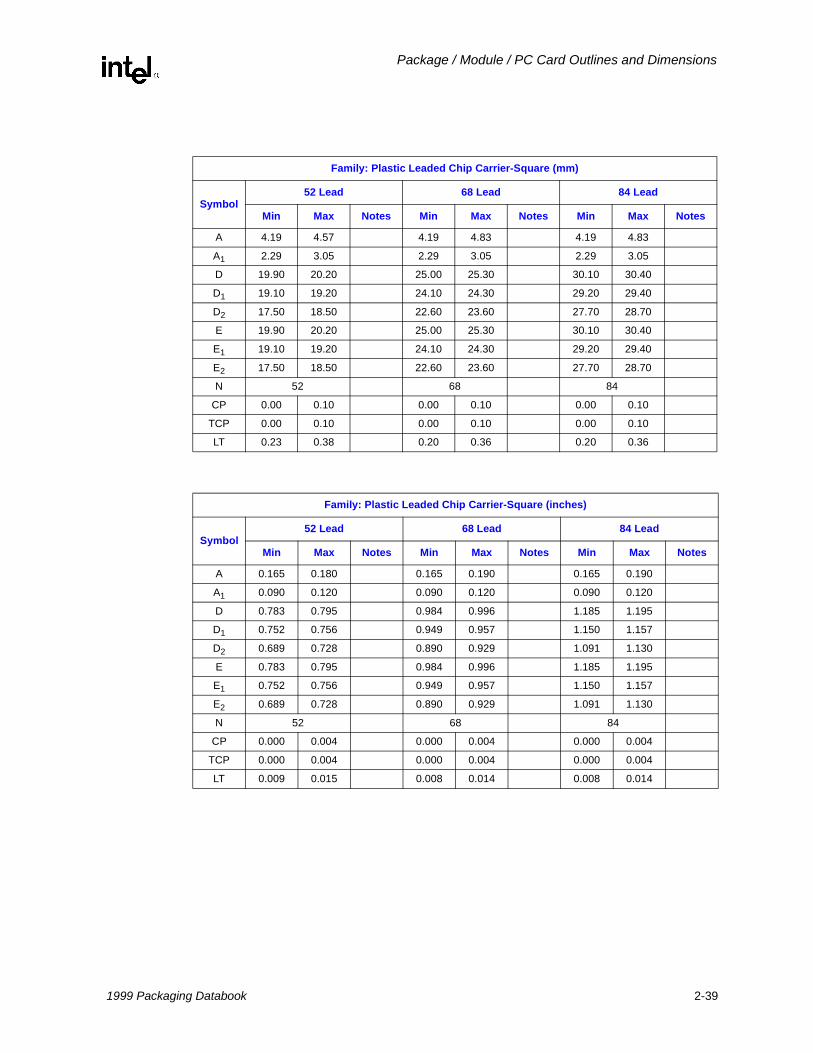
Family: Plastic Leaded Chip Carrier-Square (mm)
Symbol52 Lead 68 Lead 84 Lead
Min Max Notes Min Max Notes Min Max Notes
A 4.19 4.57 4.19 4.83 4.19 4.83
A1 2.29 3.05 2.29 3.05 2.29 3.05
D 19.90 20.20 25.00 25.30 30.10 30.40
D1 19.10 19.20 24.10 24.30 29.20 29.40
D2 17.50 18.50 22.60 23.60 27.70 28.70
E 19.90 20.20 25.00 25.30 30.10 30.40
E1 19.10 19.20 24.10 24.30 29.20 29.40
E2 17.50 18.50 22.60 23.60 27.70 28.70
N 52 68 84
CP 0.00 0.10 0.00 0.10 0.00 0.10
TCP 0.00 0.10 0.00 0.10 0.00 0.10
LT 0.23 0.38 0.20 0.36 0.20 0.36
Family: Plastic Leaded Chip Carrier-Square (inches)
Symbol52 Lead 68 Lead 84 Lead
Min Max Notes Min Max Notes Min Max Notes
A 0.165 0.180 0.165 0.190 0.165 0.190
A1 0.090 0.120 0.090 0.120 0.090 0.120
D 0.783 0.795 0.984 0.996 1.185 1.195
D1 0.752 0.756 0.949 0.957 1.150 1.157
D2 0.689 0.728 0.890 0.929 1.091 1.130
E 0.783 0.795 0.984 0.996 1.185 1.195
E1 0.752 0.756 0.949 0.957 1.150 1.157
E2 0.689 0.728 0.890 0.929 1.091 1.130
N 52 68 84
CP 0.000 0.004 0.000 0.004 0.000 0.004
TCP 0.000 0.004 0.000 0.004 0.000 0.004
LT 0.009 0.015 0.008 0.014 0.008 0.014
1999 Packaging Databook 2-39
Package / Module / PC Card Outlines and Dimensions
2.7.1.8 Principal Dimensions and Datums
2.7.1.9 Molded Detail
A5545-01
A1
D1
3
E1
0.18 (.007) SF-GS A–C–Seating Plane
Datum Plane2
0.18 (.007) SD-ES B
E
–G–3
–F–3
3
A
–D–
–H–
D
Tweezing Surface
TCP(all four sides)
11
–E–
–B –
–A–
A5546-01
BasePlane
0.51 (.020) Min
3 x 0.25 (.010 )R NOM
D1
6
3.81 (0.150)Max Typ
.002mm/mm (In/In) A
0.18 (.007) SF-GS
S
–C–
Seating Plane
1.22 (.048)1.07 (.042)
1.91 (0.075) Max Typ
51.22 (.048)1.07 (.042)
2 PLCS
E1
5
A
.002mm/mm (In/In)
0.18 (.007) -BS SD-ES B
–A–
–B–
2-40 1999 Packaging Databook
Package / Module / PC Card Outlines and Dimensions
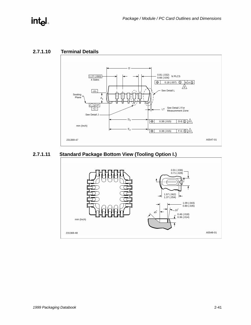
2.7.1.10 Terminal Details
2.7.1.11 Standard Package Bottom View (Tooling Option I.)
A5547-01
0.38 (.015) SD-E
0.18 (.007) SS AB
4
See Detail L
D
D2
A1
CP–C–
–H–Seating
Plane
1.27 (.050)0.81 (.032)0.66 (.026) N PLCS
See Detail J
4 Sides
0.38 (.015) SF-G 4E2
LT
4
See Detail J ForMeasurement Zone
mm (Inch)
231369-47
A5548-01
1.57 (.062)1.37 (.054)
0.46 (.018)0.36 (.014)
10˚45˚
0.91 (.036)0.71 (.028)
1.09 (.043)0.89 (.035)
mm (Inch)
231369-48
1999 Packaging Databook 2-41
Package / Module / PC Card Outlines and Dimensions
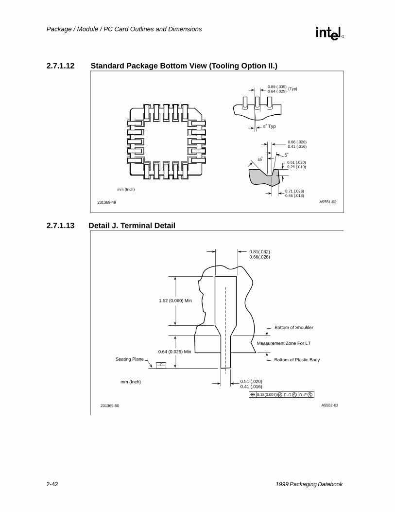
2.7.1.12 Standard Package Bottom View (Tooling Option II.)
2.7.1.13 Detail J. Terminal Detail
A5551-02
0.51 (.020)0.25 (.010)
5˚45˚
0.89 (.035)0.64 (.025)
0.66 (.026)0.41 (.016)
5˚ Typ
0.71 (.028)0.46 (.018)
mm (Inch)
(Typ)
231369-49
A5552-02
Bottom of Plastic Body
0.18(0.007) SM F–G
Bottom of Shoulder
0.51 (.020)0.41 (.016)
0.81(.032)0.66(.026)
1.52 (0.060) Min
–C–Seating Plane
0.64 (0.025) Min
Measurement Zone For LT
SD–E
mm (Inch)
231369-50
2-42 1999 Packaging Databook
Package / Module / PC Card Outlines and Dimensions
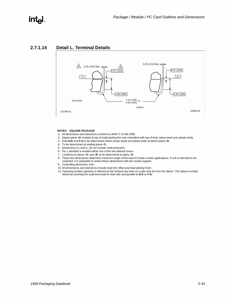
2.7.1.14 Detail L. Terminal Details
A5553-01
1.14 (.045)0.64 (.025)
–H–
1.51 (.020)
1.65 (.065)
0.25 (.010) Max
–H–
0.51 (.020)
1.65 (.065)
0.25 (.010) Max
R
8
Detail L
mm (Inch)
8
231369-51
NOTES: SQUARE PACKAGE1. All dimensions and tolerances conform to ANSI Y 14.5M-1982.2. Datum plane -H- located at top of mold parting line and coincident with top of lead, where lead exits plastic body.3. Data D-E and F-G to be determined where center leads exit plastic body at datum plane -H-.4. To be determined at seating plane -C-.5. Dimensions D1 and E1 do not include mold protrusion. 6. Pin 1 identifier is located within one of the two defined zones.7. Locations to datum -A- and -B- to be determined at plane -H-.8. These two dimensions determine maximum angle of the lead of certain socket applications. If unit is intended to be
socketed, it is advisable to review these dimensions with the socket supplier.9. Controlling dimension, inch.10. All dimensions and tolerances include lead trim offset and lead plating finish.11. Tweezing surface planarity is defined as the furthest any lead on a side may be from the datum. The datum is estab-
lished by touching the outermost lead on that side and parallel to D-E or F-G.
1999 Packaging Databook 2-43
Package / Module / PC Card Outlines and Dimensions
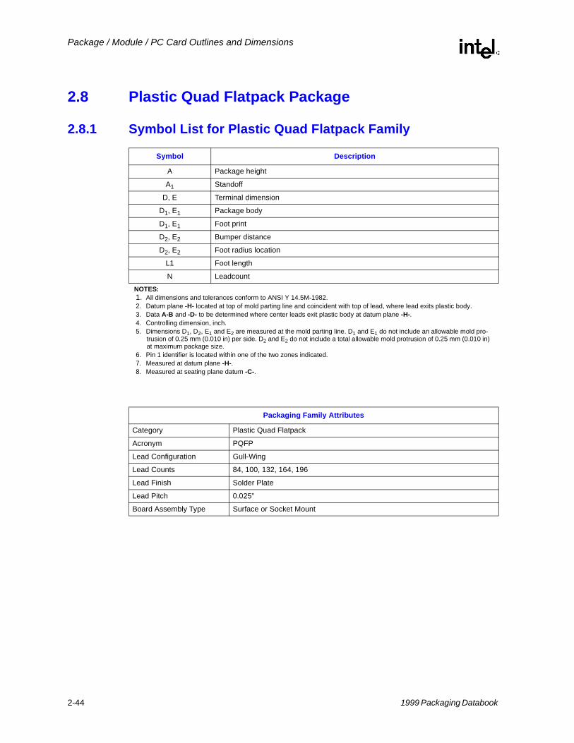
2.8 Plastic Quad Flatpack Package
2.8.1 Symbol List for Plastic Quad Flatpack Family
Symbol Description
A Package height
A1 Standoff
D, E Terminal dimension
D1, E1 Package body
D1, E1 Foot print
D2, E2 Bumper distance
D2, E2 Foot radius location
L1 Foot length
N LeadcountNOTES: 1. All dimensions and tolerances conform to ANSI Y 14.5M-1982.2. Datum plane -H- located at top of mold parting line and coincident with top of lead, where lead exits plastic body.3. Data A-B and -D- to be determined where center leads exit plastic body at datum plane -H-.4. Controlling dimension, inch.5. Dimensions D1, D2, E1 and E2 are measured at the mold parting line. D1 and E1 do not include an allowable mold pro-
trusion of 0.25 mm (0.010 in) per side. D2 and E2 do not include a total allowable mold protrusion of 0.25 mm (0.010 in) at maximum package size.
6. Pin 1 identifier is located within one of the two zones indicated.7. Measured at datum plane -H-.8. Measured at seating plane datum -C-.
Packaging Family Attributes
Category Plastic Quad Flatpack
Acronym PQFP
Lead Configuration Gull-Wing
Lead Counts 84, 100, 132, 164, 196
Lead Finish Solder Plate
Lead Pitch 0.025”
Board Assembly Type Surface or Socket Mount
2-44 1999 Packaging Databook
Package / Module / PC Card Outlines and Dimensions
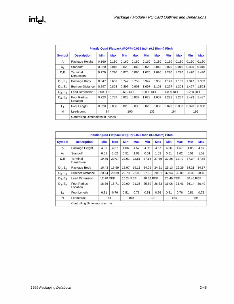
Plastic Quad Flatpack (PQFP) 0.025 Inch (0.635mm) Pitch
Symbol Description Min Max Min Max Min Max Min Max Min Max
A Package Height 0.160 0.180 0.160 0.180 0.160 0.180 0.160 0.180 0.160 0.180
A1 Standoff 0.020 0.040 0.020 0.040 0.020 0.040 0.020 0.040 0.020 0.040
D,E Terminal Dimension
0.770 0.790 0.870 0.890 1.070 1.090 1.270 1.290 1.470 1.490
D1, E1 Package Body 0.647 0.653 0.747 0.753 0.947 0.953 1.147 1.153 1.347 1.353
D2, E2 Bumper Distance 0.797 0.803 0.897 0.903 1.097 1.103 1.297 1.303 1.497 1.503
D3, E3 Lead Dimension 0.500 REF 0.600 REF 0.800 REF 1.000 REF 1.200 REF
D4, E4 Foot Radius Location
0.723.
0.737 0.823 0.837 1.023 1.037 1.223 1.237 1.423 1.437
L1 Foot Length 0.020 0.030 0.020 0.030 0.020 0.030 0.020 0.030 0.020 0.030
N Leadcount 84 100 132 164 196
Controlling Dimensions in Inches
Plastic Quad Flatpack (PQFP) 0.025 Inch (0.635mm) Pitch
Symbol Description Min Max Min Max Min Max Min Max Min Max
A Package Height 4.06 4.57 4.06 4.57 4.06 4.57 4.06 4.57 4.06 4.57
A1 Standoff 0.51 1.02 0.51 1.02 0.51 1.02 0.51 1.02 0.51 1.02
D,E Terminal Dimension
19.56 20.07 22.01 22.61 27.18 27.69 32.26 32.77 37.34 37.85
D1, E1 Package Body 16.43 16.59 18.97 19.13 24.05 24.21 29.13 29.29 34.21 34.37
D2, E2 Bumper Distance 20.24 20.39 22.78 22.93 27.86 28.01 32.94 33.09 38.02 38.18
D3, E3 Lead Dimension 12.70 REF 15.24 REF 20.32 REF 25.40 REF 30.48 REF
D4, E4 Foot Radius Location
18.36 18.71 20.90 21.25 25.89 26.33 31.06 31.41 36.14 36.49
L1 Foot Length 0.51 0.76 0.51 0.76 0.51 0.76 0.51 0.76 0.51 0.76
N Leadcount 84 100 132 164 196
Controlling Dimensions in mm
1999 Packaging Databook 2-45
Package / Module / PC Card Outlines and Dimensions
2.8.1.1 Principal Dimensions and Datums
2.8.1.2 Molded Details
A5554-01
Base Plane
A1
0.20 (.008) SAM S–BC
3–B–
3–A–
–H–2
A
0.10 (.004)–C– Seating Plane
–D– 3
D1
D2
DSD
E2 E E1
0.20 (.008) SAM S–BC SD
A5555-01
6
D1
D2
E2 E1
See Detail M
3.81 (.150) Max. Typ
S.002 MM/MM (IN/IN) A–B
1.91 (.075) Max. Typ
0.25 (.010) SAM S–BC SD
S.002 MM/MM (IN/IN) A–B0.25 (.010) SAM S–BC SD
.002 MM/MM (IN/IN) D0.25 (.010) SAM S–BC SD
S.002 MM/MM (IN/IN)0.25 (.010) SAM S–BC SD
D
2-46 1999 Packaging Databook
Package / Module / PC Card Outlines and Dimensions
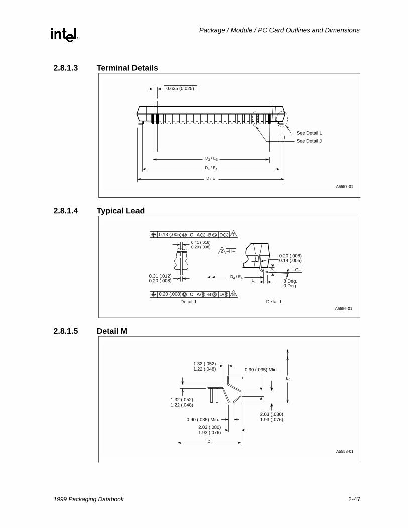
2.8.1.3 Terminal Details
2.8.1.4 Typical Lead
2.8.1.5 Detail M
See Detail J
0.635 (0.025)
D / E
D3 / E3
See Detail L
A5557-01
D4 / E4
A5556-01
0.20 (.008) SDS-BSM AC
2
L1
0.20 (.008)0.14 (.005)
–H–
8 Deg.0 Deg.
D4 / E4
0.41 (.016)0.20 (.008)
0.31 (.012)0.20 (.008)
A1 –C–
8
Detail J Detail L
0.13 (.005) SDS-BSM AC 7
A5558-01
E2
1.32 (.052)1.22 (.048)
1.32 (.052)1.22 (.048) 0.90 (.035) Min.
2.03 (.080)1.93 (.076)0.90 (.035) Min.
2.03 (.080)1.93 (.076)
D2
1999 Packaging Databook 2-47
Package / Module / PC Card Outlines and Dimensions
2.9 Quad Flatpack Package
2.9.1 Symbol List for Quad Flatpack Family
Letter or Symbol Description of Dimensions
A Overall Height
A1 Standoff
AAA Lead True Position
b Lead Width
c Lead Thickness
D Terminal Dimension
D1 Body Package
E Terminal Dimension
E1 Body Package
e1 Lead Pitch
L1 Foot Length
N Leadcount
T Lead Angle
Y CoplanarityNOTE: RECTANGLE PACKAGE1. Not all packages are available with all products. Contact local Intel Representative for further package information.
Packaging Family Attributes
Category Quad Flatpack
Acronym QFP, SQFP, TQFP
Lead Configuration Quad
Lead Counts QFP 44, 48, 64, 80, 100, 160 - SQFP 80, 100, 128, 208 - TQFP 100, 144, 176
Lead Finish Solder Plate
Lead Pitch 0. 5, 0.65, 0.8 mm
Board Assembly Type Surface or Socket MountNOTES: 1. QFP - Alloy 42/copper on some lead frames. SQFP / TQFP copper lead frames only.2. Novalac Body.3. Not all packages are available with all products. Contact local Intel Representative for further package information.
2-48 1999 Packaging Databook
Package / Module / PC Card Outlines and Dimensions
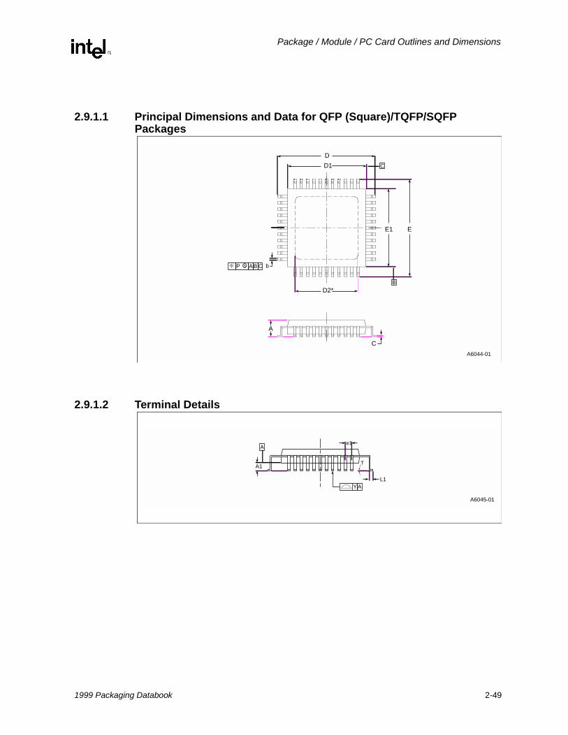
2.9.1.1 Principal Dimensions and Data for QFP (Square)/TQFP/SQFP Packages
2.9.1.2 Terminal Details
A6044-01
C
A
D2*
D1
D
E1 E
B
B CP A
C
bS
A6045-01
A
A
YL1
A1
e1
T
1999 Packaging Databook 2-49
Package / Module / PC Card Outlines and Dimensions
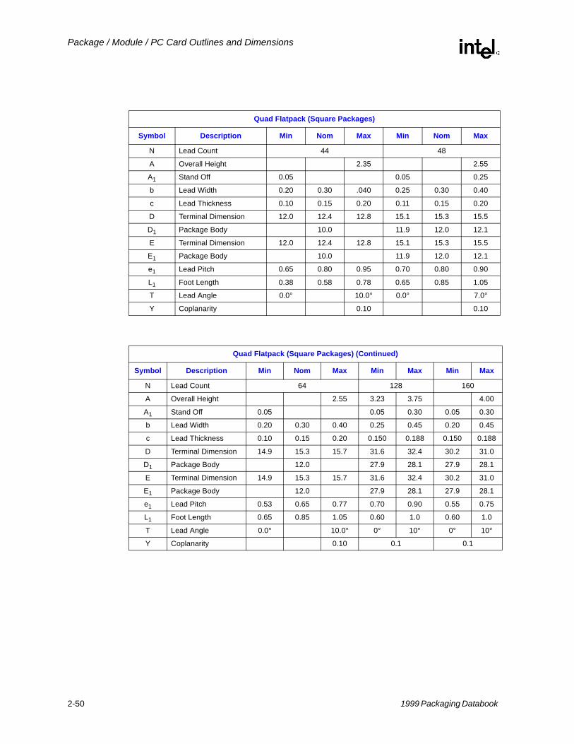
Quad Flatpack (Square Packages)
Symbol Description Min Nom Max Min Nom Max
N Lead Count 44 48
A Overall Height 2.35 2.55
A1 Stand Off 0.05 0.05 0.25
b Lead Width 0.20 0.30 .040 0.25 0.30 0.40
c Lead Thickness 0.10 0.15 0.20 0.11 0.15 0.20
D Terminal Dimension 12.0 12.4 12.8 15.1 15.3 15.5
D1 Package Body 10.0 11.9 12.0 12.1
E Terminal Dimension 12.0 12.4 12.8 15.1 15.3 15.5
E1 Package Body 10.0 11.9 12.0 12.1
e1 Lead Pitch 0.65 0.80 0.95 0.70 0.80 0.90
L1 Foot Length 0.38 0.58 0.78 0.65 0.85 1.05
T Lead Angle 0.0° 10.0° 0.0° 7.0°
Y Coplanarity 0.10 0.10
Quad Flatpack (Square Packages) (Continued)
Symbol Description Min Nom Max Min Max Min Max
N Lead Count 64 128 160
A Overall Height 2.55 3.23 3.75 4.00
A1 Stand Off 0.05 0.05 0.30 0.05 0.30
b Lead Width 0.20 0.30 0.40 0.25 0.45 0.20 0.45
c Lead Thickness 0.10 0.15 0.20 0.150 0.188 0.150 0.188
D Terminal Dimension 14.9 15.3 15.7 31.6 32.4 30.2 31.0
D1 Package Body 12.0 27.9 28.1 27.9 28.1
E Terminal Dimension 14.9 15.3 15.7 31.6 32.4 30.2 31.0
E1 Package Body 12.0 27.9 28.1 27.9 28.1
e1 Lead Pitch 0.53 0.65 0.77 0.70 0.90 0.55 0.75
L1 Foot Length 0.65 0.85 1.05 0.60 1.0 0.60 1.0
T Lead Angle 0.0° 10.0° 0° 10° 0° 10°
Y Coplanarity 0.10 0.1 0.1
2-50 1999 Packaging Databook
Package / Module / PC Card Outlines and Dimensions
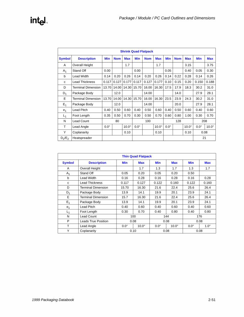
Shrink Quad Flatpack
Symbol Description Min Nom Max Min Nom Max Min Nom Max Min Max
A Overall Height 1.7 1.7 3.15 3.75
A1 Stand Off 0.00 0.00 0.05 0.40 0.05 0.30
b Lead Width 0.14 0.20 0.26 0.14 0.20 0.26 0.14 0.22 0.28 0.14 0.26
c Lead Thickness 0.117 0.127 0.177 0.117 0.127 0.177 0.10 0.15 0.20 0.150 0.188
D Terminal Dimension 13.70 14.00 14.30 15.70 16.00 16.30 17.5 17.9 18.3 30.2 31.0
D1 Package Body 12.0 14.00 14.0 27.9 28.1
E Terminal Dimension 13.70 14.00 14.30 15.70 16.00 16.30 23.5 23.9 24.3 30.2 31.0
E1 Package Body 12.0 14.00 20.0 27.9 28.1
e1 Lead Pitch 0.40 0.50 0.60 0.40 0.50 0.60 0.40 0.50 0.60 0.40 0.60
L1 Foot Length 0.35 0.50 0.70 0.30 0.50 0.70 0.60 0.80 1.00 0.30 0.70
N Lead Count 80 100 128 208
T Lead Angle 0.0° 10.0° 0.0° 10.0° 0.0° 10.0° 0.0° 10.0°
Y Coplanarity 0.10 0.10 0.10 0.08
D2/E2 Heatspreader 21
Thin Quad Flatpack
Symbol Description Min Max Min Max Min MaxA Overall Height 1.7 1.3 1.7 1.3 1.7A1 Stand Off 0.05 0.20 0.05 0.20 0.50b Lead Width 0.16 0.28 0.16 0.28 0.16 0.28c Lead Thickness 0.117 0.127 0.122 0.160 0.122 0.160D Terminal Dimension 15.70 16.30 21.6 22.4 25.6 26.4D1 Package Body 13.9 14.1 19.9 20.1 23.9 24.1E Terminal Dimension 15.7 16.30 21.6 22.4 25.6 26.4E1 Package Body 13.9 14.1 19.9 20.1 23.9 24.1e1 Lead Pitch 0.40 0.60 0.40 0.60 0.40 0.60L1 Foot Length 0.30 0.70 0.40 0.80 0.40 0.80N Lead Count 100 144 176P Leads True Position 0.08 0.08 0.08T Lead Angle 0.0° 10.0° 0.0° 10.0° 0.0° 1.0°Y Coplanarity 0.10 0.08 0.08
1999 Packaging Databook 2-51
Package / Module / PC Card Outlines and Dimensions
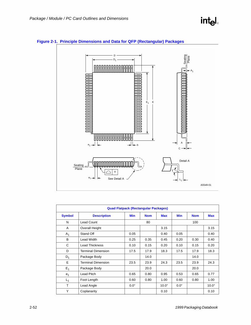
Figure 2-1. Principle Dimensions and Data for QFP (Rectangular) Packages
A5549-01
D1
E1
Sea
ting
Pla
ne
E
D
A1
C
A
SeatingPlane
See Detail A L1
Detail A
Y T
be1
e1
Quad Flatpack (Rectangular Packages)
Symbol Description Min Nom Max Min Nom Max
N Lead Count 80 100
A Overall Height 3.15 3.15
A1 Stand Off 0.05 0.40 0.05 0.40
B Lead Width 0.25 0.35 0.45 0.20 0.30 0.40
C Lead Thickness 0.10 0.15 0.20 0.10 0.15 0.20
D Terminal Dimension 17.5 17.9 18.3 17.5 17.9 18.3
D1 Package Body 14.0 14.0
E Terminal Dimension 23.5 23.9 24.3 23.5 23.9 24.3
E1 Package Body 20.0 20.0
e1 Lead Pitch 0.65 0.80 0.95 0.53 0.65 0.77
L1 Foot Length 0.60 0.80 1.00 0.60 0.80 1.00
T Lead Angle 0.0° 10.0° 0.0° 10.0°
Y Coplanarity 0.10 0.10
2-52 1999 Packaging Databook

Package / Module / PC Card Outlines and Dimensions
2.10 Small Out-line J-lead Package (SOJ)
2.10.1 Symbol List for Small Out-Line J-Lead Family
Letter or Symbol Description of Dimensions
A Overall Height
A2 Distance from Base Plane to Highest Point of Body (Lid)
B Width of Terminal Leads
B1 Width of Terminal Lead Shoulder Which Locate Seating Plane (Standoff Geometry Optional)
D Largest Overall Package Dimension of Length
E Largest Over Package Width Dimension Outside of Leads
E1 Body Width Dimension Not Including Leads
e1 Linear Spacing Between Center Line of Body Terminal Leads (Standoffs)
eA Linear Spacing of True Minimum Lead Position Center Line to Center Line
N Total Number of Potentially Usable Lead Positions
Packaging Family Attributes
Category Small Outline J-Lead
Acronym SOJ
Lead Configuration Dual-In-Line
Lead Counts 20, 24
Lead Finish Solder Plate
Lead Pitch 0.050”
Board Assembly Type Surface MountNOTES: 1. Alloy 42 Leads.2. Novalac body.
1999 Packaging Databook 2-53
Package / Module / PC Card Outlines and Dimensions
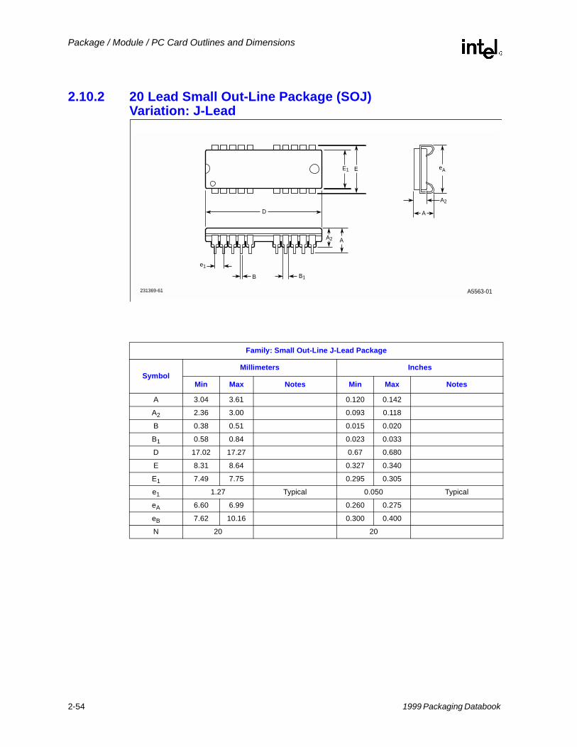
2.10.2 20 Lead Small Out-Line Package (SOJ) Variation: J-Lead
A5563-01
D
A2
A
A
B B1
E1 E
e1
eA
231369-61
A2
Family: Small Out-Line J-Lead Package
SymbolMillimeters Inches
Min Max Notes Min Max Notes
A 3.04 3.61 0.120 0.142
A2 2.36 3.00 0.093 0.118
B 0.38 0.51 0.015 0.020
B1 0.58 0.84 0.023 0.033
D 17.02 17.27 0.67 0.680
E 8.31 8.64 0.327 0.340
E1 7.49 7.75 0.295 0.305
e1 1.27 Typical 0.050 Typical
eA 6.60 6.99 0.260 0.275
eB 7.62 10.16 0.300 0.400
N 20 20
2-54 1999 Packaging Databook
Package / Module / PC Card Outlines and Dimensions
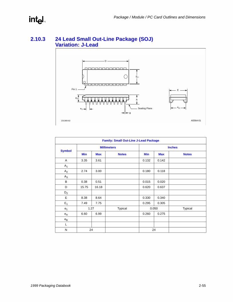
2.10.3 24 Lead Small Out-Line Package (SOJ) Variation: J-Lead
A5564-01
D
A2
E
A
B
E1
e1eA
Pin 1
Seating Plane
231369-62
Family: Small Out-Line J-Lead Package
SymbolMillimeters Inches
Min Max Notes Min Max Notes
A 3.35 3.61 0.132 0.142
A1
A2 2.74 3.00 0.180 0.118
A3
B 0.38 0.51 0.015 0.020
D 15.75 16.18 0.620 0.637
D2
E 8.38 8.64 0.330 0.340
E1 7.49 7.75 0.295 0.305
e1 1.27 Typical 0.050 Typical
eA 6.60 6.99 0.260 0.275
eB
L
N 24 24
1999 Packaging Databook 2-55
Package / Module / PC Card Outlines and Dimensions
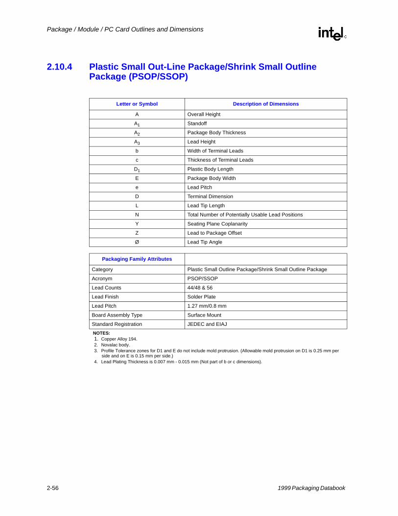
2.10.4 Plastic Small Out-Line Package/Shrink Small Outline Package (PSOP/SSOP)
Letter or Symbol Description of Dimensions
A Overall Height
A1 Standoff
A2 Package Body Thickness
A3 Lead Height
b Width of Terminal Leads
c Thickness of Terminal Leads
D1 Plastic Body Length
E Package Body Width
e Lead Pitch
D Terminal Dimension
L Lead Tip Length
N Total Number of Potentially Usable Lead Positions
Y Seating Plane Coplanarity
Z Lead to Package Offset
Ø Lead Tip Angle
Packaging Family Attributes
Category Plastic Small Outline Package/Shrink Small Outline Package
Acronym PSOP/SSOP
Lead Counts 44/48 & 56
Lead Finish Solder Plate
Lead Pitch 1.27 mm/0.8 mm
Board Assembly Type Surface Mount
Standard Registration JEDEC and EIAJNOTES: 1. Copper Alloy 194.2. Novalac body.3. Profile Tolerance zones for D1 and E do not include mold protrusion. (Allowable mold protrusion on D1 is 0.25 mm per
side and on E is 0.15 mm per side.)4. Lead Plating Thickness is 0.007 mm - 0.015 mm (Not part of b or c dimensions).
2-56 1999 Packaging Databook
Package / Module / PC Card Outlines and Dimensions
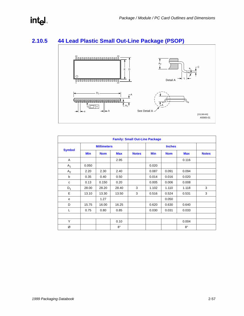
2.10.5 44 Lead Plastic Small Out-Line Package (PSOP)
A5565-01
A1
A
b
DE
e See Detail A
A2
0
LDetail A
Y
D1
44 23
1 22
A
C
[231369-80]
Family: Small Out-Line Package
SymbolMillimeters Inches
Min Nom Max Notes Min Nom Max Notes
A 2.95 0.116
A1 0.050 0.020
A2 2.20 2.30 2.40 0.087 0.091 0.094
b 0.35 0.40 0.50 0.014 0.016 0.020
c 0.13 0.150 0.20 0.005 0.006 0.008
D1 28.00 28.20 28.40 3 1.102 1.110 1.118 3
E 13.10 13.30 13.50 3 0.516 0.524 0.531 3
e 1.27 0.050
D 15.75 16.00 16.25 0.620 0.630 0.640
L 0.75 0.80 0.85 0.030 0.031 0.033
Y 0.10 0.004
Ø 8° 8°
1999 Packaging Databook 2-57
Package / Module / PC Card Outlines and Dimensions
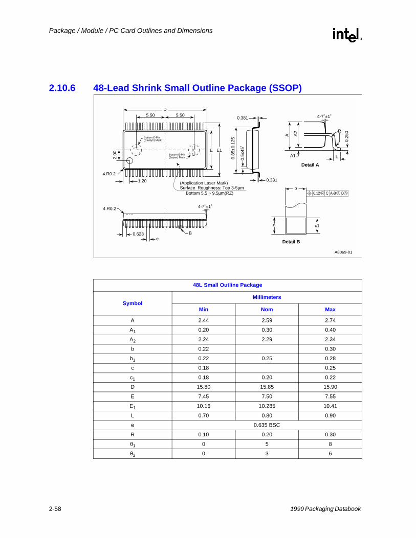
2.10.6 48-Lead Shrink Small Outline Package (SSOP)
A8069-01
D
E
B
4-7˚±1˚
4-7˚±1˚
A1E1
5.505.502.
00
A2
0.25
0
A
0.5x
45˚
0.85
±0.
125
1.20
0.381
0.381
b
L
R
c1c
0.623
(Application Laser Mark)Surface Roughness: Top 3-5µm
Bottom 5.5 ~ 9.5µm(RZ)
e
4.R0.2
4.R0.2
Bottom E-Pin(Cavity#) Mark
Bottom E-Pin(Japan) Mark
C DA-B S SM0.12
Detail B
Detail A
48L Small Outline Package
SymbolMillimeters
Min Nom Max
A 2.44 2.59 2.74
A1 0.20 0.30 0.40
A2 2.24 2.29 2.34
b 0.22 0.30
b1 0.22 0.25 0.28
c 0.18 0.25
c1 0.18 0.20 0.22
D 15.80 15.85 15.90
E 7.45 7.50 7.55
E1 10.16 10.285 10.41
L 0.70 0.80 0.90
e 0.635 BSC
R 0.10 0.20 0.30
θ1 0 5 8
θ2 0 3 6
2-58 1999 Packaging Databook
Package / Module / PC Card Outlines and Dimensions
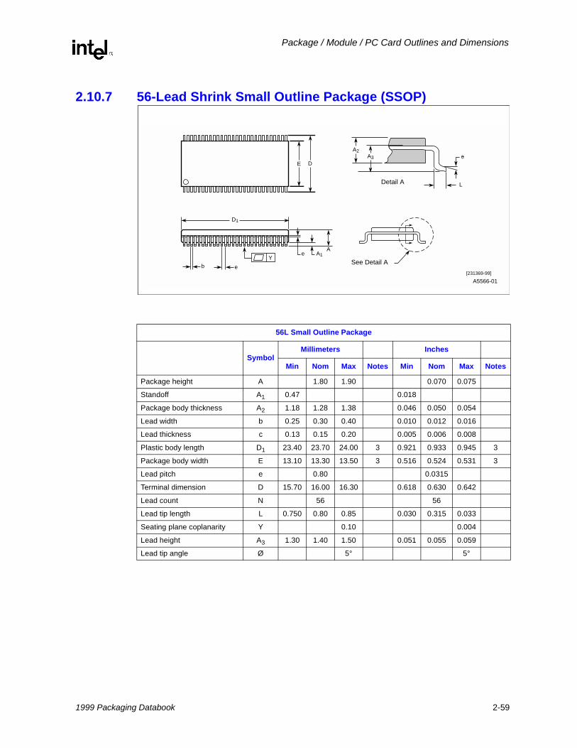
2.10.7 56-Lead Shrink Small Outline Package (SSOP)
A5566-01
A1A
b
DE
e
e
See Detail A
A2A3 0
LDetail A
D1
Y
[231369-99]
56L Small Outline Package
SymbolMillimeters Inches
Min Nom Max Notes Min Nom Max Notes
Package height A 1.80 1.90 0.070 0.075
Standoff A1 0.47 0.018
Package body thickness A2 1.18 1.28 1.38 0.046 0.050 0.054
Lead width b 0.25 0.30 0.40 0.010 0.012 0.016
Lead thickness c 0.13 0.15 0.20 0.005 0.006 0.008
Plastic body length D1 23.40 23.70 24.00 3 0.921 0.933 0.945 3
Package body width E 13.10 13.30 13.50 3 0.516 0.524 0.531 3
Lead pitch e 0.80 0.0315
Terminal dimension D 15.70 16.00 16.30 0.618 0.630 0.642
Lead count N 56 56
Lead tip length L 0.750 0.80 0.85 0.030 0.315 0.033
Seating plane coplanarity Y 0.10 0.004
Lead height A3 1.30 1.40 1.50 0.051 0.055 0.059
Lead tip angle Ø 5° 5°
1999 Packaging Databook 2-59

Package / Module / PC Card Outlines and Dimensions
2.11 Thin Small Out-line Package (TSOP)Note: For more SOP package information refer to SOP package guide Order #296514.
2.11.1 Symbol List for Thin Small Out-Line Package Family
Letter or Symbol Description of Dimensions
A Overall Height
A1 Standoff
A2 Package Body Thickness
A3 Lead Height
b Width of Terminal Leads
c Thickness of Terminal Leads
D Terminal Dimension
D1 Plastic Body Length
E Package Body Width
e Lead Pitch
L Lead Foot Length
N Total Number of Potentially Usable Lead Positions
Y Seating Plane Coplanarity
Z Lead to Package Offset
Ø Lead Tip Angle
Packaging Family Attributes
Category Thin Small Out-Line Package
Acronym TSOP
Lead Configuration Dual-In-Line, Type I
Lead Counts 32, 40, 48, 56
Lead Finish Solder Plate
Lead Pitch 0.5 mm
Board Assembly Type Surface MountNOTES: 1. Alloy 42 Leads.2. Novalac body.3. Offered in Reverse Pin-Out for special circuit layout, (32L, 40L only).4. Profile Tolerance zones for D1 and E do not include mold protrusion. (Allowable mold protrusion on D1 is 0.25 mm per
side and on E is 0.15 mm per side.)5. Lead plating thickness is 0.007 mm - 0.015 mm (Not part of b or c dimensions).
2-60 1999 Packaging Databook
Package / Module / PC Card Outlines and Dimensions
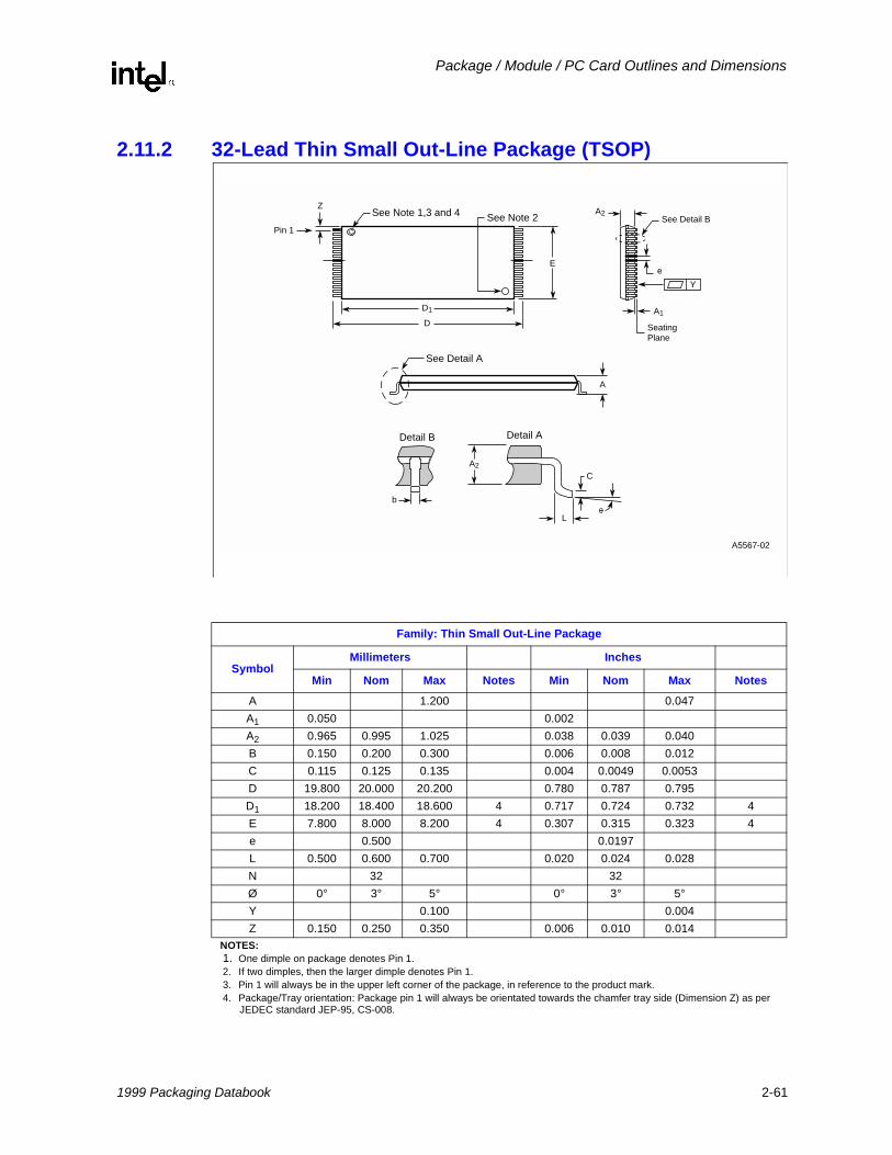
2.11.2 32-Lead Thin Small Out-Line Package (TSOP)
A5567-02
A
A2
L
Detail A
Y
D
See Note 2
E
D1
0
C
b
Detail B
See Detail A
See Note 1,3 and 4
e
See Detail B
A1
Z
Pin 1
A2
SeatingPlane
Family: Thin Small Out-Line Package
SymbolMillimeters Inches
Min Nom Max Notes Min Nom Max NotesA 1.200 0.047A1 0.050 0.002A2 0.965 0.995 1.025 0.038 0.039 0.040B 0.150 0.200 0.300 0.006 0.008 0.012C 0.115 0.125 0.135 0.004 0.0049 0.0053D 19.800 20.000 20.200 0.780 0.787 0.795D1 18.200 18.400 18.600 4 0.717 0.724 0.732 4E 7.800 8.000 8.200 4 0.307 0.315 0.323 4e 0.500 0.0197L 0.500 0.600 0.700 0.020 0.024 0.028N 32 32Ø 0° 3° 5° 0° 3° 5°Y 0.100 0.004Z 0.150 0.250 0.350 0.006 0.010 0.014
NOTES: 1. One dimple on package denotes Pin 1.2. If two dimples, then the larger dimple denotes Pin 1.3. Pin 1 will always be in the upper left corner of the package, in reference to the product mark. 4. Package/Tray orientation: Package pin 1 will always be orientated towards the chamfer tray side (Dimension Z) as per
JEDEC standard JEP-95, CS-008.
1999 Packaging Databook 2-61
Package / Module / PC Card Outlines and Dimensions
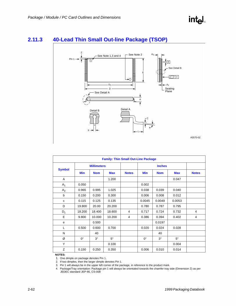
2.11.3 40-Lead Thin Small Out-line Package (TSOP)
A5570-02
A
0
L
Detail A
Y
D
C
Z
Pin 1
E
D1
b
Detail B
e
A1
SeatingPlane
A2See Note 2See Note 1,3 and 4
See Detail A
See Detail B
Family: Thin Small Out-Line Package
SymbolMillimeters Inches
Min Nom Max Notes Min Nom Max Notes
A 1.200 0.047
A1 0.050 0.002
A2 0.965 0.995 1.025 0.038 0.039 0.040
b 0.150 0.200 0.300 0.006 0.008 0.012
c 0.115 0.125 0.135 0.0045 0.0049 0.0053
D 19.800 20.00 20.200 0.780 0.787 0.795
D1 18.200 18.400 18.600 4 0.717 0.724 0.732 4
E 9.800 10.000 10.200 4 0.386 0.394 0.402 4
e 0.500 0.0197
L 0.500 0.600 0.700 0.020 0.024 0.028
N 40 40
Ø 0° 3° 5° 0° 3° 5°
Y 0.100 0.004
Z 0.150 0.250 0.350 0.006 0.010 0.014NOTES: 1. One dimple on package denotes Pin 1.2. If two dimples, then the larger dimple denotes Pin 1.3. Pin 1 will always be in the upper left corner of the package, in reference to the product mark.4. Package/Tray orientation: Package pin 1 will always be orientated towards the chamfer tray side (Dimension Z) as per
JEDEC standard JEP-95, CS-008
2-62 1999 Packaging Databook
Package / Module / PC Card Outlines and Dimensions
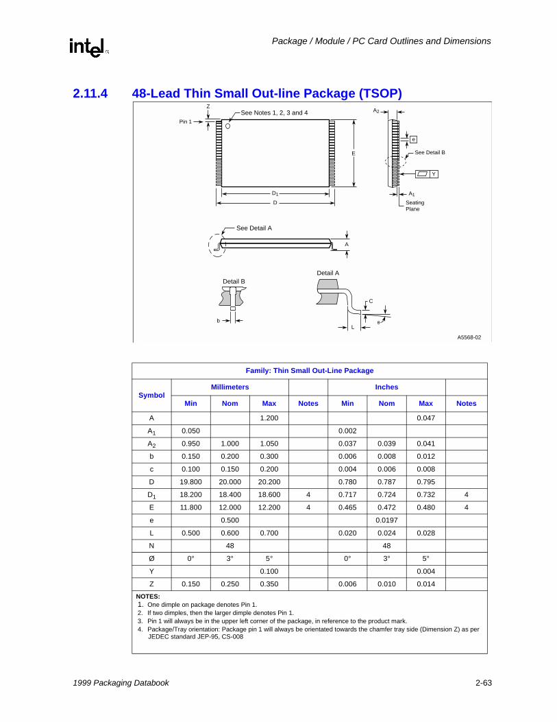
2.11.4 48-Lead Thin Small Out-line Package (TSOP)
A5568-02
A
0L
Detail A
Y
D
C
Z
Pin 1
E
D1
b
Detail B
See Detail A
e
See Detail B
A1
A2
SeatingPlane
See Notes 1, 2, 3 and 4
Family: Thin Small Out-Line Package
SymbolMillimeters Inches
Min Nom Max Notes Min Nom Max Notes
A 1.200 0.047
A1 0.050 0.002
A2 0.950 1.000 1.050 0.037 0.039 0.041
b 0.150 0.200 0.300 0.006 0.008 0.012
c 0.100 0.150 0.200 0.004 0.006 0.008
D 19.800 20.000 20.200 0.780 0.787 0.795
D1 18.200 18.400 18.600 4 0.717 0.724 0.732 4
E 11.800 12.000 12.200 4 0.465 0.472 0.480 4
e 0.500 0.0197
L 0.500 0.600 0.700 0.020 0.024 0.028
N 48 48
Ø 0° 3° 5° 0° 3° 5°
Y 0.100 0.004
Z 0.150 0.250 0.350 0.006 0.010 0.014NOTES: 1. One dimple on package denotes Pin 1.2. If two dimples, then the larger dimple denotes Pin 1.3. Pin 1 will always be in the upper left corner of the package, in reference to the product mark.4. Package/Tray orientation: Package pin 1 will always be orientated towards the chamfer tray side (Dimension Z) as per
JEDEC standard JEP-95, CS-008
1999 Packaging Databook 2-63
Package / Module / PC Card Outlines and Dimensions
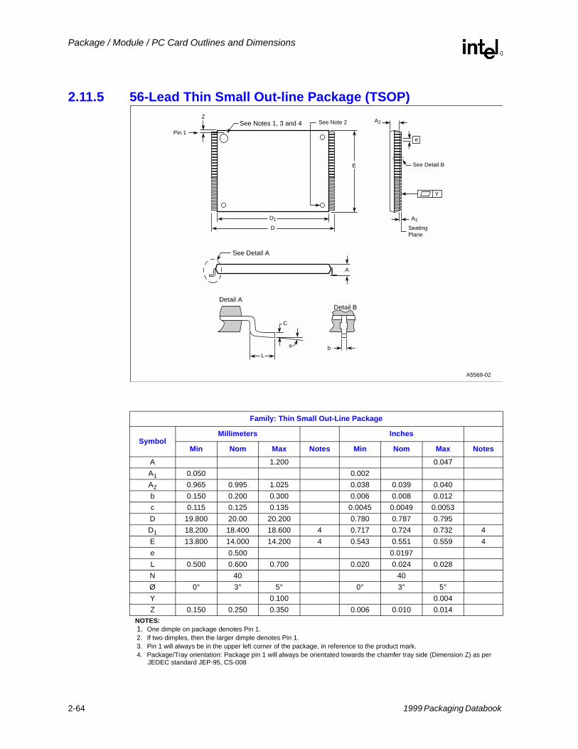
2.11.5 56-Lead Thin Small Out-line Package (TSOP)
A5569-02
A
0
L
Detail A
Y
D
C
Z
Pin 1
E
D1
b
Detail B
See Detail A
e
See Detail B
A1
SeatingPlane
A2See Note 2See Notes 1, 3 and 4
Family: Thin Small Out-Line Package
SymbolMillimeters Inches
Min Nom Max Notes Min Nom Max NotesA 1.200 0.047A1 0.050 0.002A2 0.965 0.995 1.025 0.038 0.039 0.040b 0.150 0.200 0.300 0.006 0.008 0.012c 0.115 0.125 0.135 0.0045 0.0049 0.0053D 19.800 20.00 20.200 0.780 0.787 0.795D1 18.200 18.400 18.600 4 0.717 0.724 0.732 4E 13.800 14.000 14.200 4 0.543 0.551 0.559 4e 0.500 0.0197L 0.500 0.600 0.700 0.020 0.024 0.028N 40 40Ø 0° 3° 5° 0° 3° 5°Y 0.100 0.004Z 0.150 0.250 0.350 0.006 0.010 0.014
NOTES: 1. One dimple on package denotes Pin 1.2. If two dimples, then the larger dimple denotes Pin 1.3. Pin 1 will always be in the upper left corner of the package, in reference to the product mark.4. Package/Tray orientation: Package pin 1 will always be orientated towards the chamfer tray side (Dimension Z) as per
JEDEC standard JEP-95, CS-008
2-64 1999 Packaging Databook
Package / Module / PC Card Outlines and Dimensions
2.12 Pinned Packages
2.12.1 Plastic Pin Grid Array (PPGA)For package drawings and dimensions of the PPGA package please refer to Chapter 13.
2.12.2 Micro Pin Grid Array (µPGA)For package drawings and dimensions of the µPGA package please refer to Chapter 13.
2.12.3 Flip Chip PGA (FC-PGA)For package drawings and dimensions of the FC-PGA package please refer to Chapter 13.
2.13 Ball Grid Array Packages
2.13.1 Plastic Ball Grid Array (PBGA)For package drawings and dimensions of the PBGA package please refer to Chapter 14.
2.13.2 Organic Land Grid Array (OLGA)For package drawings and dimensions of the OLGA package please refer to Chapter 14.
2.14 Chip Scale Packages (CSP)
2.14.1 Micro Ball Grid Array (µBGA)For package drawings and dimensions of the OLGA package please refer to Chapter 15.
2.14.2 Easy BGAFor package drawings and dimensions of the Easy BGA package please refer to Chapter 15.
2.14.3 Intel® Stacked CSPFor package drawings and dimensions of the Easy BGA package please refer to Chapter 15.
2.14.4 Molded Matrix Array Package (MMAP)For package drawings and dimensions of the Easy BGA package please refer to Chapter 15.
1999 Packaging Databook 2-65
Package / Module / PC Card Outlines and Dimensions
2.15 Cartridge Packaging
2.15.1 Single Edge Contact Cartridge (S.E.C.C.)For package drawings and dimensions of the S.E.C.C. package please refer to Chapter 16.
2.15.2 Single Edge Processor Package (S.E.P.P.)For package drawings and dimensions of the S.E.P.P. package please refer to Chapter 16.
2.15.3 Mobile Mini-CartridgeFor package drawings and dimensions of the Mobile Mini-Cartridge package please refer to Chapter 16.
2.16 Single In-line Leaded Memory Module Package (SIP)
2.16.1 Symbol List for Single In-Line Leaded Memory Module Family
Letter or Symbol Description of Dimensions
A2 Overall Height
B Width of Terminal Leads
C Thickness of Terminal Leads
D Largest Overall Package Dimension of Length
E Largest Overall Package Width Dimension Outside of Leads
e1 Linear Spacing between Centerline of body Terminal Leads (Standoffs)
L Distance from Seating Plane to End of Lead
Packaging Family Attributes
Category Single In-Line Leaded Package
Acronym SIP
Lead Configuration Single Row
Lead Counts 30
Lead Finish Tin/Nickel
Lead Pitch 2.5mm
Board Assembly Type Socket and Insertion Mount
2-66 1999 Packaging Databook
Package / Module / PC Card Outlines and Dimensions
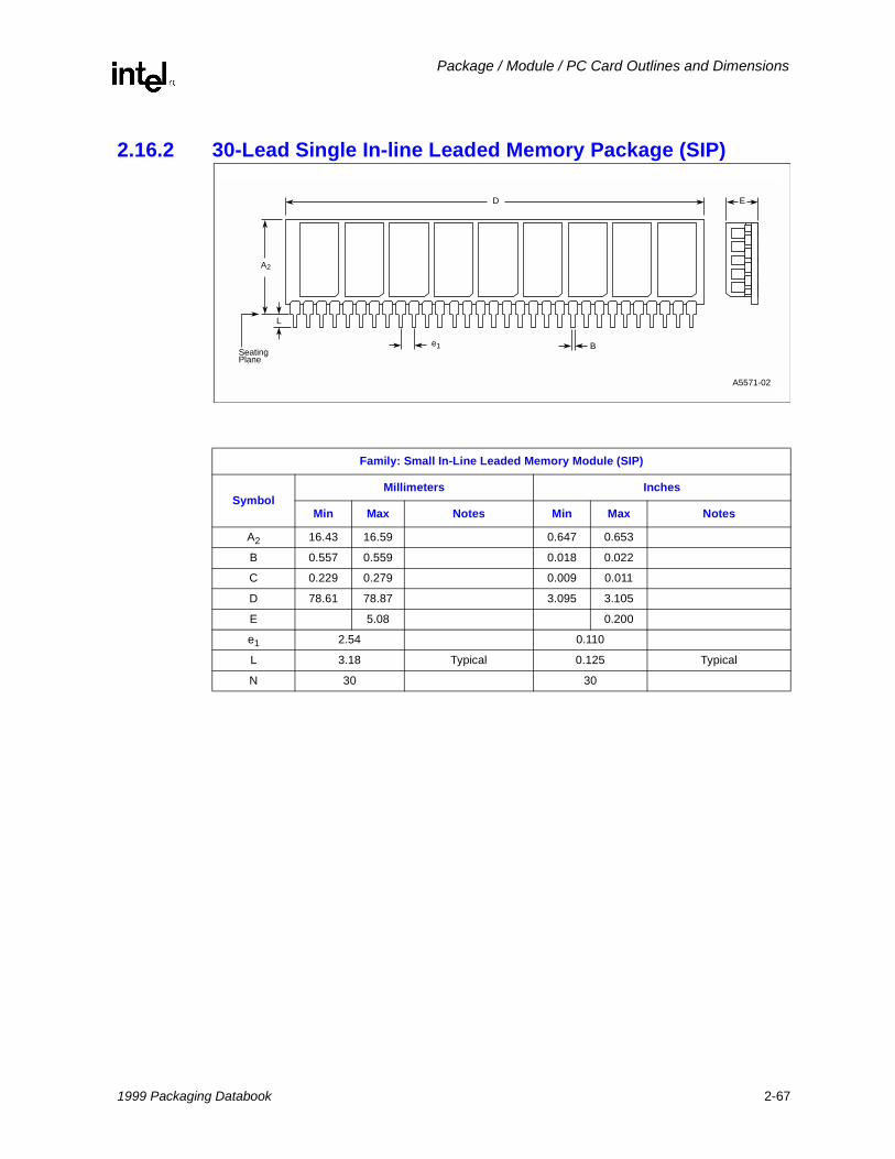
2.16.2 30-Lead Single In-line Leaded Memory Package (SIP)
A5571-02
A2
E
Be1SeatingPlane
D
L
Family: Small In-Line Leaded Memory Module (SIP)
SymbolMillimeters Inches
Min Max Notes Min Max Notes
A2 16.43 16.59 0.647 0.653
B 0.557 0.559 0.018 0.022
C 0.229 0.279 0.009 0.011
D 78.61 78.87 3.095 3.105
E 5.08 0.200
e1 2.54 0.110
L 3.18 Typical 0.125 Typical
N 30 30
1999 Packaging Databook 2-67
Package / Module / PC Card Outlines and Dimensions
2.17 Single In-line Leadless Memory Module (SIMM)
2.17.1 Symbol List for Single In-Line Leadless Memory Module Family
Letter or Symbol Description of Dimensions
B Width of Terminal Pads
C Thickness of Terminal Pads
D Largest Overall Package Dimension of Length
E Largest Overall Package Width Dimension Outside of Pads
e1 Linear Spacing between Centerline of body Terminal Pads(Standoffs)
N Total Number of Potentially Usable Lead Positions
Packaging Family Attributes
Category Single In-Line Leadless Memory Module
Acronym SIMM
Lead Configuration Single Row
Lead Counts 30, 80
Lead Finish Solder Coat
Lead Pitch 0.100”
Board Assembly Type Socket and Insertion Mount
2-68 1999 Packaging Databook

Package / Module / PC Card Outlines and Dimensions
2.17.2 30 Pad Single In-Line Leadless Memory Module (SIMM)
A5572-01
e1
D
20.4
5 M
ax
6.35
± 0
.13
10.1
6 ±
0.1
3
0 3.18 ± 0.05
3.38Top View
C
ESide View
B
231369-68
Family: Single In-Line Leadless Memory Module
SymbolMillimeters Inches
Min Max Notes Min Max Notes
B 1.78 Typical 0.070 Typical
C 1.19 1.40 0.047 0.055
D 88.77 89.03 3.495 3.505
E 5.08 0.200
e1 2.54 Typical 0.100 Typical
N 30 30
1999 Packaging Databook 2-69
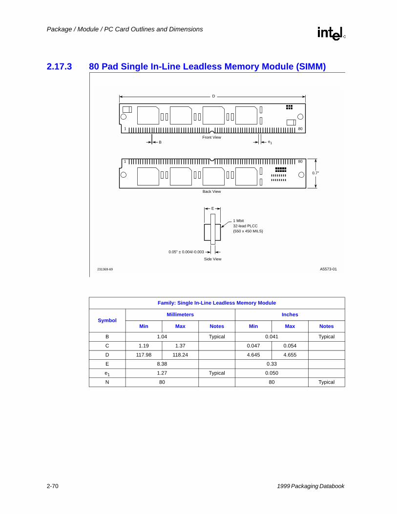
Package / Module / PC Card Outlines and Dimensions
2.17.3 80 Pad Single In-Line Leadless Memory Module (SIMM)
A5573-01
e1
D
Front View
E
1 80
B
Back View
1 80
0.7"
0.05" ± 0.004/-0.003
1 Mbit32-lead PLCC(550 x 450 MILS)
Side View
231369-69
Family: Single In-Line Leadless Memory Module
SymbolMillimeters Inches
Min Max Notes Min Max Notes
B 1.04 Typical 0.041 Typical
C 1.19 1.37 0.047 0.054
D 117.98 118.24 4.645 4.655
E 8.38 0.33
e1 1.27 Typical 0.050
N 80 80 Typical
2-70 1999 Packaging Databook
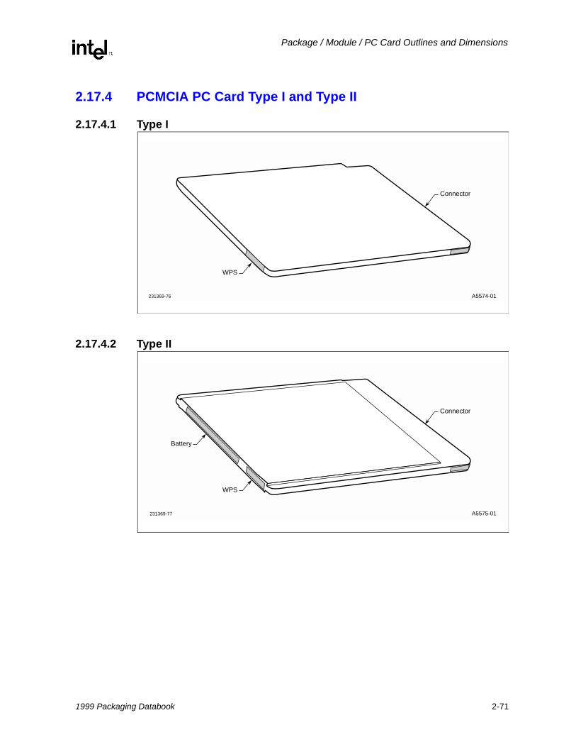
Package / Module / PC Card Outlines and Dimensions
2.17.4 PCMCIA PC Card Type I and Type II
2.17.4.1 Type I
2.17.4.2 Type II
A5574-01231369-76
WPS
Connector
A5575-01231369-77
WPS
Connector
Battery
1999 Packaging Databook 2-71
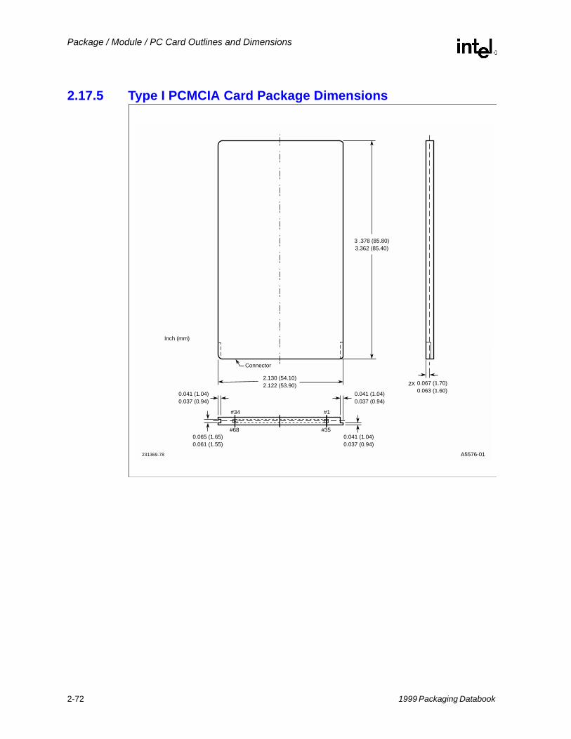
Package / Module / PC Card Outlines and Dimensions
2.17.5 Type I PCMCIA Card Package Dimensions
A5576-01
2.130 (54.10)2.122 (53.90)
3 .378 (85.80)3.362 (85.40)
231369-78
Connector
0.041 (1.04)0.037 (0.94)
0.065 (1.65)0.061 (1.55)
0.041 (1.04)0.037 (0.94)
0.041 (1.04)0.037 (0.94)
#34
#68
#1
#35
0.067 (1.70)0.063 (1.60)
2X
Inch (mm)
2-72 1999 Packaging Databook

Package / Module / PC Card Outlines and Dimensions
2.17.6 Type II PCMCIA Card Package Dimensions
A5577-01231369-82
2.130 (54.10)2.122 (53.90)
3 .378 (85.80)3.362 (85.40)
Connector
0.041 (1.04)0.037 (0.94)
0.065 (1.65)0.061 (1.55)
0.041 (1.04)0.037 (0.94)
0.041 (1.04)0.037 (0.94)
#34
#68
#1
#35
0.067 (1.70)0.063 (1.60)
2X
Substrate Area
Interconnect Area
Protect
Battery
mm (Inch)
1999 Packaging Databook 2-73
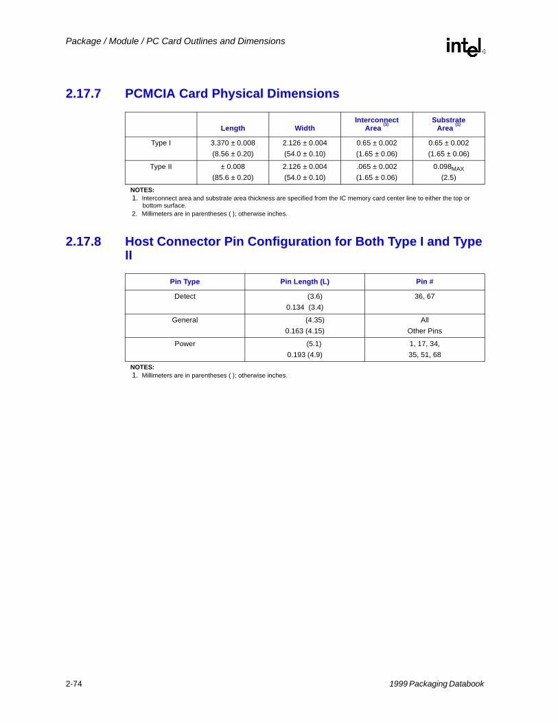
Package / Module / PC Card Outlines and Dimensions
2.17.7 PCMCIA Card Physical Dimensions
2.17.8 Host Connector Pin Configuration for Both Type I and Type II
Length WidthInterconnect
Area (1)Substrate
Area (1)
Type I 3.370 ± 0.008(8.56 ± 0.20)
2.126 ± 0.004(54.0 ± 0.10)
0.65 ± 0.002(1.65 ± 0.06)
0.65 ± 0.002(1.65 ± 0.06)
Type II ± 0.008(85.6 ± 0.20)
2.126 ± 0.004(54.0 ± 0.10)
.065 ± 0.002(1.65 ± 0.06)
0.098MAX(2.5)
NOTES: 1. Interconnect area and substrate area thickness are specified from the IC memory card center line to either the top or
bottom surface.2. Millimeters are in parentheses ( ); otherwise inches.
Pin Type Pin Length (L) Pin #
Detect (3.6)0.134 (3.4)
36, 67
General (4.35)0.163 (4.15)
AllOther Pins
Power (5.1)0.193 (4.9)
1, 17, 34,35, 51, 68
NOTES: 1. Millimeters are in parentheses ( ); otherwise inches.
2-74 1999 Packaging Databook
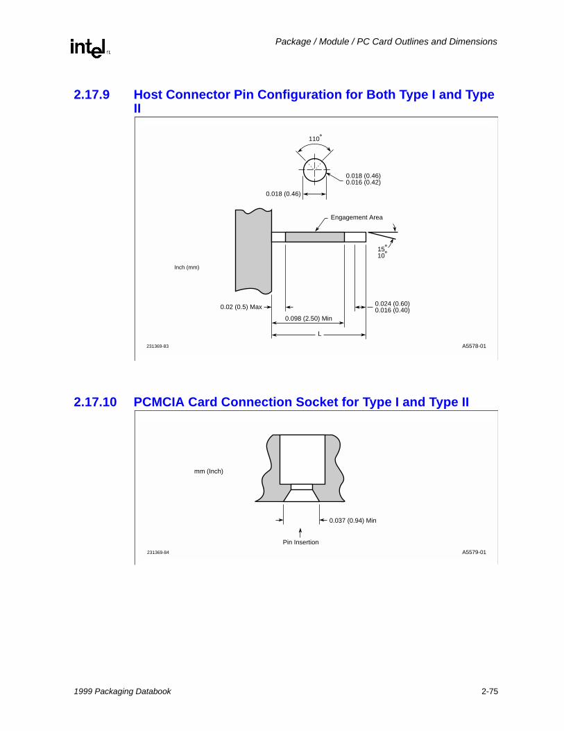
Package / Module / PC Card Outlines and Dimensions
2.17.9 Host Connector Pin Configuration for Both Type I and Type II
2.17.10 PCMCIA Card Connection Socket for Type I and Type II
A5578-01
Engagement Area
231369-83
0.02 (0.5) Max
0.098 (2.50) Min
0.024 (0.60)0.016 (0.40)
L
15˚10˚
0.018 (0.46)0.016 (0.42)
110˚
0.018 (0.46)
Inch (mm)
A5579-01
Pin Insertion
231369-84
0.037 (0.94) Min
mm (Inch)
1999 Packaging Databook 2-75
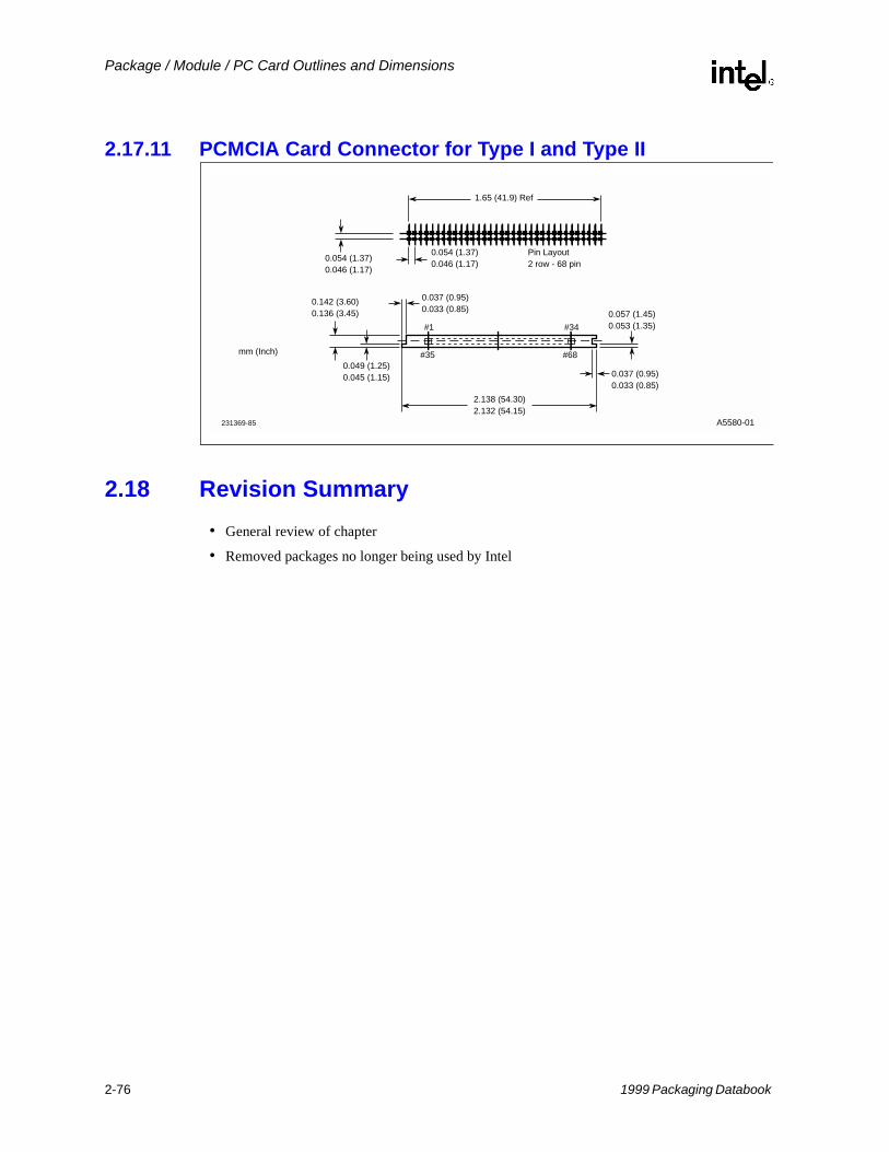
Package / Module / PC Card Outlines and Dimensions
2.17.11 PCMCIA Card Connector for Type I and Type II
2.18 Revision Summary• General review of chapter
• Removed packages no longer being used by Intel
A5580-01231369-85
0.142 (3.60)0.136 (3.45)
0.049 (1.25)0.045 (1.15)
0.057 (1.45)0.053 (1.35)
0.037 (0.95)0.033 (0.85)
#1
#35
#34
#68
2.138 (54.30)2.132 (54.15)
0.037 (0.95)0.033 (0.85)
0.054 (1.37)0.046 (1.17)
Pin Layout2 row - 68 pin
0.054 (1.37)0.046 (1.17)
1.65 (41.9) Ref
mm (Inch)
2-76 1999 Packaging Databook