Overview Booth’s Algorithm revisited Computer Internal Memory Cache memory.
63
Overview • Booth’s Algorithm revisited • Computer Internal Memory • Cache memory
-
date post
22-Dec-2015 -
Category
Documents
-
view
228 -
download
0
Transcript of Overview Booth’s Algorithm revisited Computer Internal Memory Cache memory.

Overview
• Booth’s Algorithm revisited
• Computer Internal Memory
• Cache memory

Booth’s Algorithm Revisited

2’s Comp MultiplicationBooth’s Algorithm
Q-1

2’s Comp MultiplicationBooth’s Algorithm

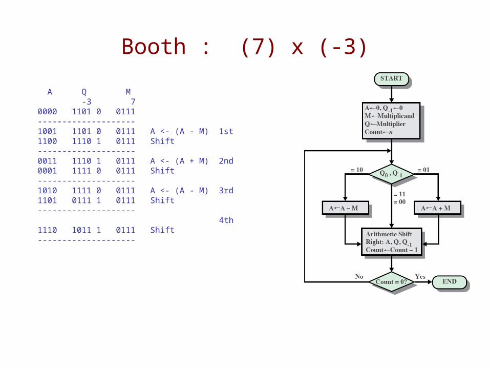
Booth : (7) x (3)
A Q M
3 7
0000 0011 0 0111
--------------------
1001 0011 0 0111 A <- (A - M) 1st
1100 1001 1 0111 Shift
--------------------
2nd
1110 0100 1 0111 Shift
--------------------
0101 0100 1 0111 A <- (A + M) 3rd
0010 1010 0 0111 Shift
--------------------
4th
0001 0101 0 0111 Shift
--------------------
Booth : (7) x (-3)
A Q M -3 7 0000 1101 0 0111 -------------------- 1001 1101 0 0111 A <- (A - M) 1st 1100 1110 1 0111 Shift -------------------- 0011 1110 1 0111 A <- (A + M) 2nd 0001 1111 0 0111 Shift -------------------- 1010 1111 0 0111 A <- (A - M) 3rd 1101 0111 1 0111 Shift -------------------- 4th 1110 1011 1 0111 Shift --------------------

Booth : (-7) x (3)
A Q M 3 -7 0000 0011 0 1001 -------------------- 0111 0011 0 1001 A <- (A - M) 1st 0011 1001 1 1001 Shift -------------------- 2nd 0001 1100 1 1001 Shift -------------------- 1010 1100 1 1001 A <- (A + M) 3rd 1101 0110 0 1001 Shift -------------------- 4th 1110 1011 0 1001 Shift --------------------
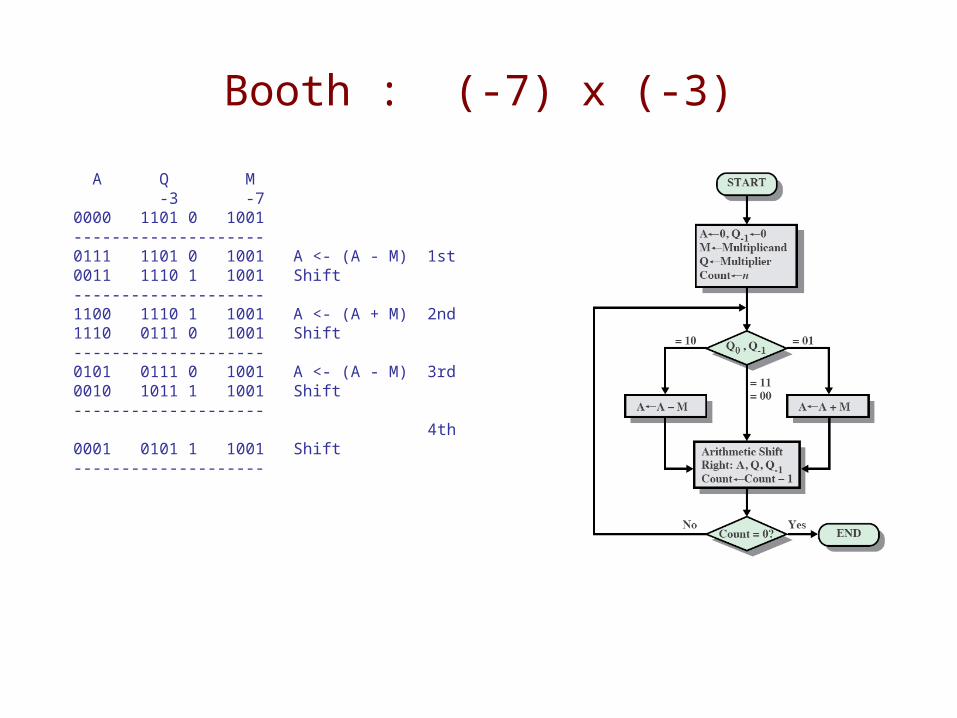
Booth : (-7) x (-3)
A Q M -3 -7 0000 1101 0 1001 -------------------- 0111 1101 0 1001 A <- (A - M) 1st 0011 1110 1 1001 Shift -------------------- 1100 1110 1 1001 A <- (A + M) 2nd 1110 0111 0 1001 Shift -------------------- 0101 0111 0 1001 A <- (A - M) 3rd 0010 1011 1 1001 Shift -------------------- 4th 0001 0101 1 1001 Shift --------------------

Computer Memory

Characteristics of Computer Memory
• Physical Location
• Capacity
• Unit of transfer
• Access Method
• Performance
• Physical Type
• Physical Characteristics
• Organization
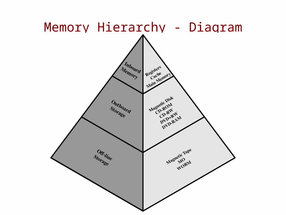
Memory Hierarchy - Diagram

Location of Memory• In CPU
• Internal to processor
• External to processor (peripheral device)
Capacity of Memory
• Word Size-The natural unit of organization
• Number of words- or Bytes

Unit of Transfer
• If Internal– Usually governed by data bus width
• If External– Usually a block which is much larger than a word
Addressable Unit
• Smallest location which can be uniquely addressed
• Word internally• Cluster on disks

Access Methods
• Sequential– Start at the beginning and read through in order– Access time depends on location of data and previous location e.g. tape
• Direct– Individual blocks have unique address– Alternatively
Access is by jumping to vicinity plus sequential searchAccess time depends on location and previous locatio e.g. disk
• Random- Individual addresses identify locations exactly e.g. RAM
• Associative - Data is located by a comparison with contents of a portion of the store - Access time is independent of location or previous access e.g. cache

Performance
• Access time– Time between presenting the address and getting the
valid data
• Memory Cycle time– Time may be required for the memory to “recover” before
next access– Cycle time is access + read/recovery (maybe rewrite)
• Transfer Rate– Rate at which data can be moved

Physical Types• Semiconductor
– RAM (SRAM, DRAM), ROM
• Magnetic– Disk & Tape
• Optical– CD & DVD [& Magneto-optical (MO)]
• Others– Bubble– Hologram– ……
Characteristics
• Volatility
• Persistence (or decay)
• Erasable
• Power consumption

The Bottom Line
• How much?– Capacity
• How fast?– Access / Transfer Rate
• How expensive?– $$$$
• Power usage?– watts

Hierarchy ListCapacity/Speed/Expense/Power
• Registers
• Cache
• Main memory
• Disk
• Tape

Internal Memory
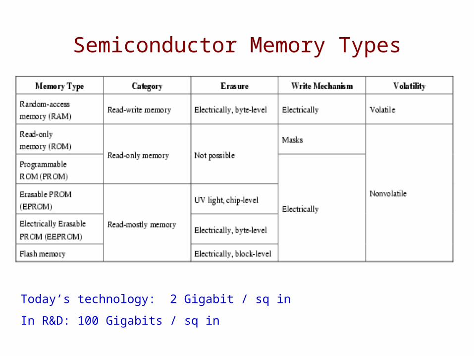
Semiconductor Memory Types
Today’s technology: 2 Gigabit / sq in
In R&D: 100 Gigabits / sq in

Semiconductor Memory (EPROM)

Static RAM (SRAM)
• Desired for main memory
– Basically an array of flip-flops
– Simple to interface and control
– Fast
– Relatively low density – complex
– Relatively expensive
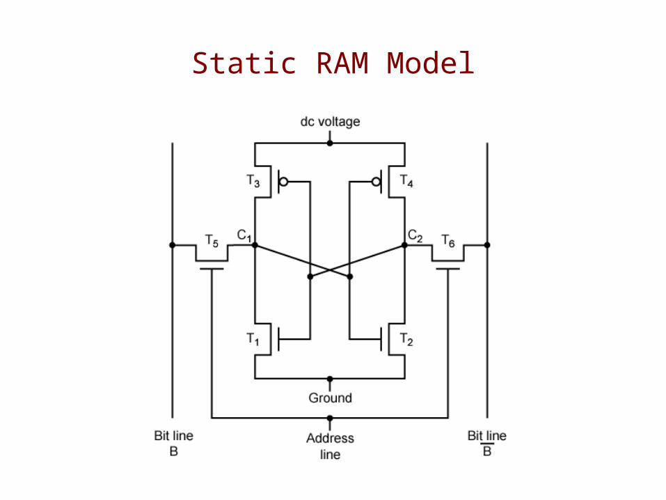
Static RAM Model

Memory Design – 1K x 4
A[00:09] D[03:00]
Addr Block Select

Memory Design – 1K x 8
A[00:09] D[07:04]
A[00:09] D[03:00]
Addr Block Select => Addr Block Select =>
D[07:04] D[03:00]
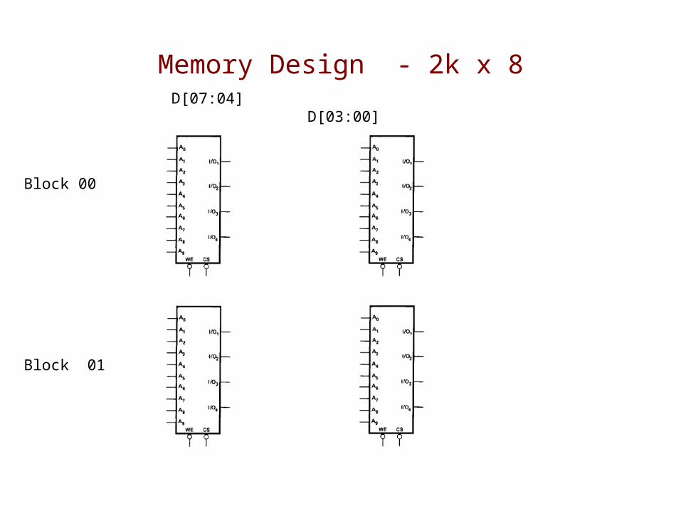
Memory Design - 2k x 8D[07:04] D[03:00]
Block 00
Block 01

Memory Design - 4k x 8 D[07:04] D[03:00]
Block 00
Block 01
Block 10
Block 11

Register

22 x 3 Memory
addressdecoder
word select word WEaddress
writeenable
input bits
output bits Multiplexor Multiplexor

24 x 8 Memory
?

1K X 4 SRAM (Part Number 2114N)
The implementation of 1K by 4 SRAM chips may differ. This implementation perhaps appears overly complex. However, its interface will be the same as others.

Memory Organization
• A 16Mbit chip can be organized as 1M of 16 bit words (likely for SRAM)
OR
• A 16Mbit chip can be organized as a 2048 x 2048 x 4bit array (likely for DRAM)– Reduces number of address pins
• Multiplex row address and column address• 11 pins to address (211=2048)• Adding one more pin doubles range of values so x4
capacity

Dynamic RAM (DRAM)
• Used in main memory– Particularly larger main memory
• Bits stored as charge in capacitors - Essentially analog device– Charges leak
• Need refreshing even when powered– Need refresh circuits
• Higher density than SRAM (more bits per chip)– Less devices/bit
• Slower than SRAM– Must refresh
• Less expensive than SRAM– More bits per area
• Less power than SRAM– Basically capacitors

Dynamic RAM model

Typical 16 Mb DRAM (4M x 4)

256kByte Module Organization (256K x 8)
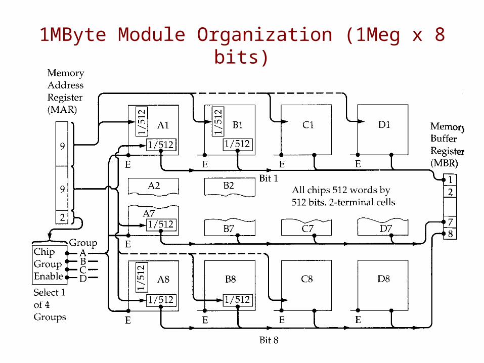
1MByte Module Organization (1Meg x 8 bits)
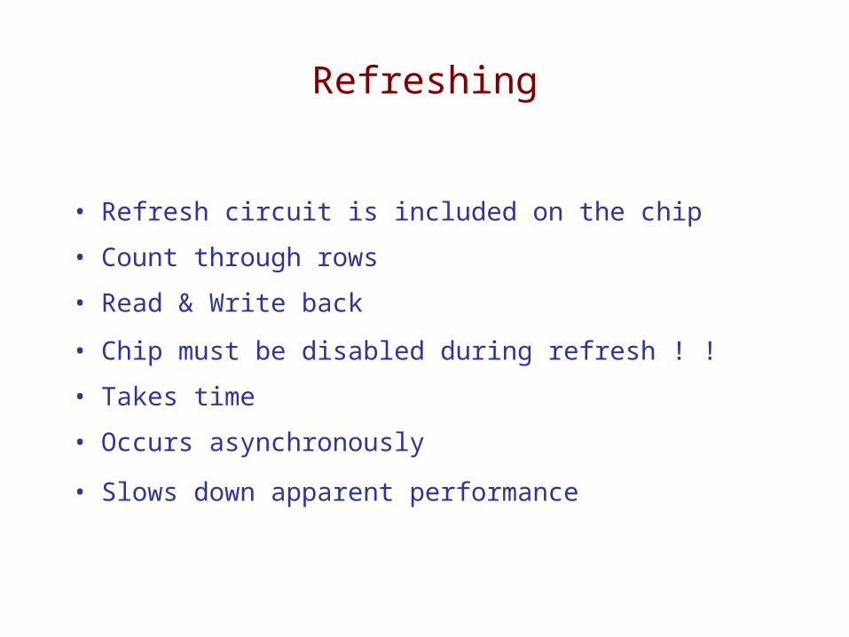
Refreshing
• Refresh circuit is included on the chip
• Count through rows
• Read & Write back
• Chip must be disabled during refresh ! !
• Takes time
• Occurs asynchronously
• Slows down apparent performance

Improvements in memory
RAM – continually gets denser.
DRAM – Several improvements: SDRAM – synchronous DRAM DDR-SDRAM - doubles transfer speed RDRAM – asynchronous one transfer per clock cycle

Cache Memory
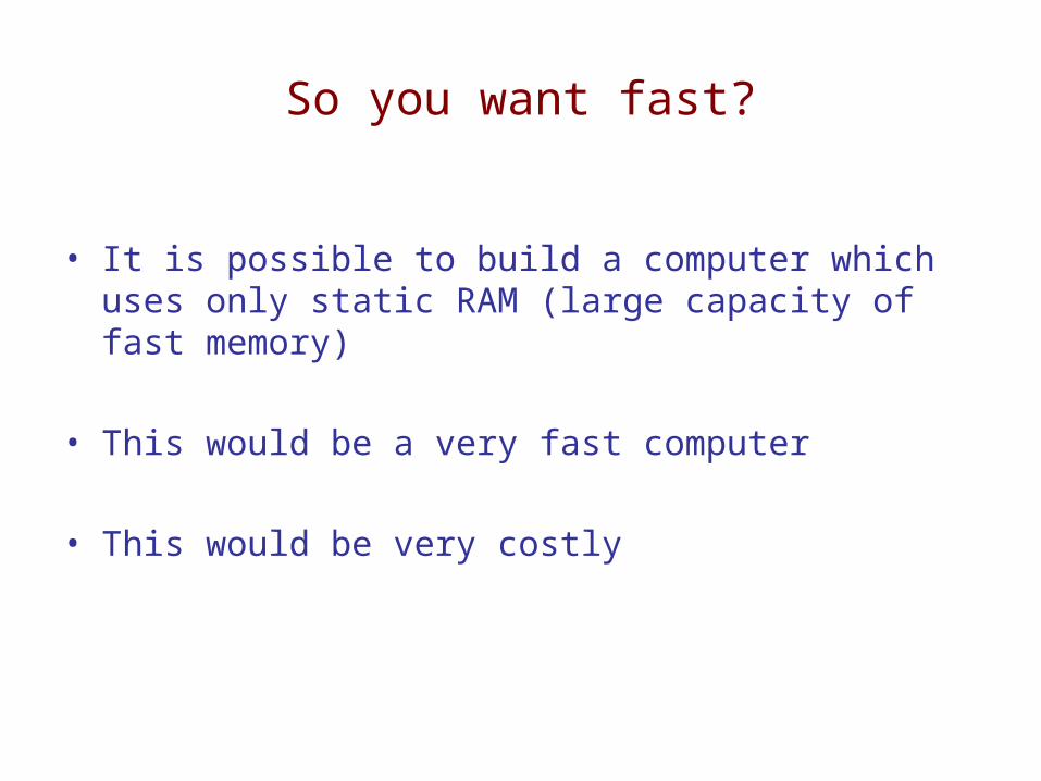
So you want fast?
• It is possible to build a computer which uses only static RAM (large capacity of fast memory)
• This would be a very fast computer
• This would be very costly

Locality of Reference
• During the course of the execution of a program, memory references tend to cluster
• e.g. programs -loops, nesting, … data – strings, lists, arrays, …

Cache Memory Organization
• Cache - Small amount of fast memory
– Sits between normal main memory and CPU
– May be located on CPU chip or in system
– Objective is to make slower memory system look like fast memory.
There may be more levels of cache (L1, L2,..)

Cache operation – Overview
• CPU requests contents of memory location
• Cache is checked for this data
• If present, get from cache (fast)
• If not present, read required block from main memory to cache
• Then deliver from cache to CPU
• Cache includes tags to identify which block(s) of main memory are in the cache

Cache Read Operation - Flowchart

Cache Design Parameters
• Size of Cache
• Size of Blocks in Cache
• Mapping Function – how to assign blocks
• Write Policy - Replacement Algorithm when blocks need to be replaced
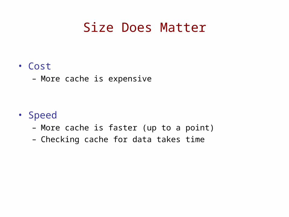
Size Does Matter
• Cost– More cache is expensive
• Speed– More cache is faster (up to a point)– Checking cache for data takes time

Typical Cache Organization

Cache/Main Direct Caching Memory Structure

Direct Mapping Cache Organization

Direct Mapping Summary
• Each block of main memory maps to only one cache line– i.e. if a block is in cache, it must be in one specific place
• Address is in two parts
- Least Significant w bits identify unique word
- Most Significant s bits specify which one memory block
• The MSBs are split into a cache line field r and a tag of s-r (most significant)

Example Direct Mapping Function
• 16MBytes main memory– i.e. memory address is 24 bits - (224=16M) bytes of memory
• Cache of 64k bytes– i.e. cache is 16k - (214) lines of 4 bytes each
• Cache block of 4 bytes– i.e. block is 4 bytes - (22) bytes of data per block

Example Direct Mapping Address Structure
Tag s-r Line or Slot r Word w
8 14 2
• 24 bit address
• 2 bit word identifier (4 byte block)
• 22 bit block identifier– 8 bit tag (=22-14)– 14 bit slot or line
• No two blocks in the same line have the same Tag field
• Check contents of cache by finding line and checking Tag

Illustrationof Example
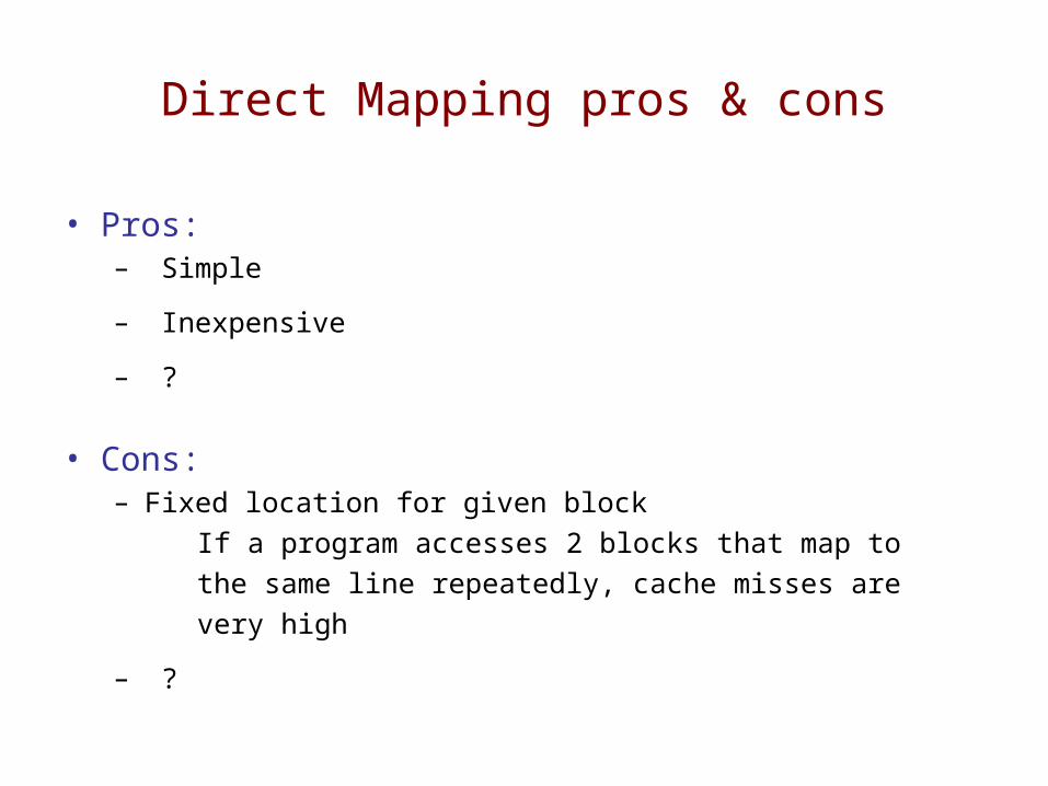
Direct Mapping pros & cons
• Pros:– Simple
– Inexpensive
– ?
• Cons:– Fixed location for given block If a program accesses 2 blocks that map to the same line repeatedly, cache misses are very high
– ?

The remaining slides in this set were not covered in class.

Comparison of improved DRAM
Conventional DRAM – 40 to 100 MB/S transfer rate?
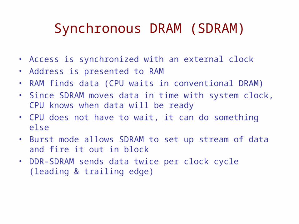
Synchronous DRAM (SDRAM)
• Access is synchronized with an external clock• Address is presented to RAM• RAM finds data (CPU waits in conventional DRAM)• Since SDRAM moves data in time with system clock, CPU
knows when data will be ready• CPU does not have to wait, it can do something else• Burst mode allows SDRAM to set up stream of data and fire
it out in block• DDR-SDRAM sends data twice per clock cycle (leading &
trailing edge)

SDRAM Read Timing

SDRAM

DDR SDRAM
• SDRAM can only send data once per clock• Double-data-rate SDRAM can send data twice per
clock cycle– Rising edge and falling edge
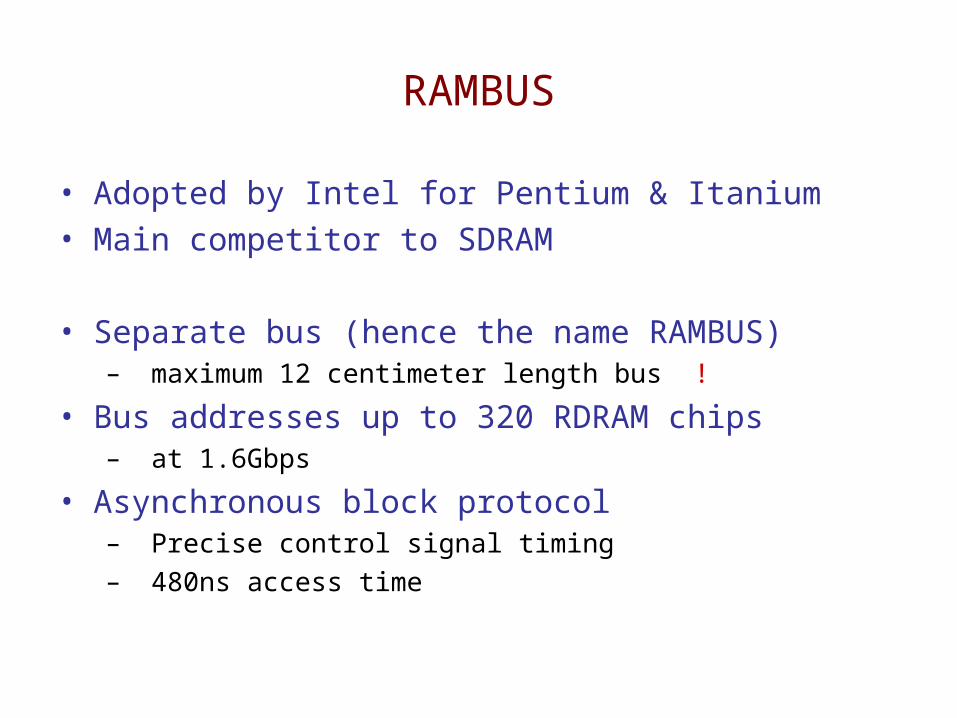
RAMBUS
• Adopted by Intel for Pentium & Itanium• Main competitor to SDRAM
• Separate bus (hence the name RAMBUS)– maximum 12 centimeter length bus !
• Bus addresses up to 320 RDRAM chips – at 1.6Gbps
• Asynchronous block protocol– Precise control signal timing– 480ns access time
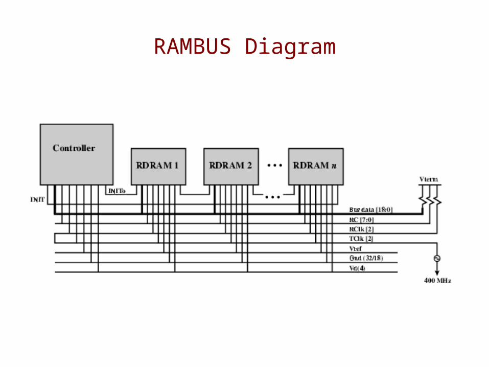
RAMBUS Diagram