
Outline:
11
- 1 - ernational Conference on Position Sensitive Detectors ernational Conference on Position Sensitive Detectors, Leicester Leicester 1 11/09 09/200 /2002 Yu.Gornushkin [email protected] Yu.Gornushkin [email protected] Outline: G. Claus, C. Colledani, G. Deptuch, M.Deveaux, W. Dulinski, A.Gay, Yu. Gornushkin , A.Himmi, Ch. Hu-Guo, I.Valin, and M. Winter IReS and LEPSI, IN2P3/ULP, 23, rue du Loess BP 23 (BP 20), F-67037 Strasbourg, France Tracking Performances and Radiation Tracking Performances and Radiation Tolerance of Tolerance of Monolithic Monolithic Active Active Pixel Sensors. Pixel Sensors. * Principle of operation of CMOS sensors Principle of operation of CMOS sensors Resent results with first small prototypes (resolution, rad.toleran Resent results with first small prototypes (resolution, rad.toleran Performances of 1 Performances of 1 st st real scale prototype (3.5 cm real scale prototype (3.5 cm 2 , 1 million pixels) , 1 million pixels) Status of 1 Status of 1 st st prototype with column parallel readout and prototype with column parallel readout and integrated CDS integrated CDS Summary Summary
-
Upload
rosalyn-peterson -
Category
Documents
-
view
21 -
download
0
description
Tracking Performances and Radiation Tolerance of Monolithic Active Pixel Sensors. G. Claus, C. Colledani, G. Deptuch, M.Deveaux, W. Dulinski, A.Gay, Yu. Gornushkin , A.Himmi, Ch. Hu-Guo, I.Valin, and M. Winter - PowerPoint PPT Presentation
Transcript of Outline:

- 1 -
66thth International Conference on Position Sensitive Detectors International Conference on Position Sensitive Detectors ,, Leicester Leicester 1 111//0909/200/20022Yu.Gornushkin [email protected] [email protected]
Outline:
G. Claus, C. Colledani, G. Deptuch, M.Deveaux, W. Dulinski, A.Gay, Yu. Gornushkin, A.Himmi, Ch. Hu-Guo, I.Valin,
and M. Winter IReS and LEPSI, IN2P3/ULP,
23, rue du Loess BP 23 (BP 20), F-67037 Strasbourg, France
Tracking Performances and Tracking Performances and Radiation Tolerance of Radiation Tolerance of Monolithic Monolithic
Active Pixel Sensors.Active Pixel Sensors.
*
•Principle of operation of CMOS sensorsPrinciple of operation of CMOS sensors•Resent results with first small prototypes (resolution, rad.tolerance)Resent results with first small prototypes (resolution, rad.tolerance)•Performances of 1Performances of 1stst real scale prototype (3.5 cm real scale prototype (3.5 cm22 , 1 million pixels) , 1 million pixels)•Status of 1Status of 1stst prototype with column parallel readout and prototype with column parallel readout and integrated CDSintegrated CDS•SummarySummary

- 2 -
66thth International Conference on Position Sensitive Detectors International Conference on Position Sensitive Detectors ,, Leicester Leicester 1 111//0909/200/20022Yu.Gornushkin [email protected] [email protected]
Idea and principle of Idea and principle of operationoperation
Twin-tub (double well) CMOS process with moderately doped epitaxial layer providing long minority carrier lifetime
• Charge is generated in epitaxial layer (low doping): Q~80e--h/m• Charge is collected through thermal diffusion by n-well/p-epi diode• No depletion potential applied • Potential barriers at layer interfaces confine the charge – improving
collection efficiency• Charge-Voltage conversion on pixel• The device can be fabricated using a standard CMOS process,• P-type low resistivity Si only NMOS transistors allowed
Titre :figure5_xfig.epsAuteur :fig2dev Version 3.2 Patchlevel 1Aperçu :Cette image EPS n'a pas été enregistréeavec un aperçu intégré.Commentaires :Cette image EPS peut être imprimée sur uneimprimante PostScript mais pas surun autre type d'imprimante.
• CMOS MAPS are replacing CCDs in visible light applications (still and video cameras, web-cameras, cell phones) – low power consumption, cheap!
To use them also for m.i.p. detection
In Strasbourg (IReS-LEPSI) since 1999

- 3 -
66thth International Conference on Position Sensitive Detectors International Conference on Position Sensitive Detectors ,, Leicester Leicester 1 111//0909/200/20022Yu.Gornushkin [email protected] [email protected]
First Prototypes - Summary of PerformancesFirst Prototypes - Summary of PerformancesMIMOSA I
die size 3.6 × 4.2 mm2
Dev
ice
inte
rnal
arc
hit
ectu
re
e.g.
MIM
OS
A I
I
Examples of pixel layouts
M I: 20× 20 µm2
High performances in m.i.p. detection established: S/N~30, >99%,sp~1.5-2 m

- 4 -
66thth International Conference on Position Sensitive Detectors International Conference on Position Sensitive Detectors ,, Leicester Leicester 1 111//0909/200/20022Yu.Gornushkin [email protected] [email protected]
Recent MIMOSA-1 resultsRecent MIMOSA-1 resultsTitre :
Auteur :ROOT Version3.02/01Aperçu :Cette image EPS n'a pas été enregistréeavec un aperçu intégré.Commentaires :Cette image EPS peut être imprimée sur uneimprimante PostScript mais pas surun autre type d'imprimante.
Titre :
Auteur :ROOT Version3.02/01Aperçu :Cette image EPS n'a pas été enregistréeavec un aperçu intégré.Commentaires :Cette image EPS peut être imprimée sur uneimprimante PostScript mais pas surun autre type d'imprimante.
Real particle clusters overlapped and combined distribution approximated by charge distribution function fot 2 hits.
Hits are well separated at distances > 30 m.
The spatial resolution as a function of ADC-bit encoding ( real signals “digitized” offline): even with 3-4 bits ~2-3 m

- 5 -
66thth International Conference on Position Sensitive Detectors International Conference on Position Sensitive Detectors ,, Leicester Leicester 1 111//0909/200/20022Yu.Gornushkin [email protected] [email protected]
MIMOSA-4 test results:MIMOSA-4 test results:
0.35 mm AMS process without epitaxial layer but with low doping (resistivity) substrate
Observed performances with 120 GeV/c p- at CERN-SPS:•Detection efficiency ~99.7%•S/N ~30 but charge spread is wider•Spatial resolution ~4 m (20 m pitch)
Technology without epitaxial layer seems worth investigating and optimizingTechnology without epitaxial layer seems worth investigating and optimizing
•p-substrate process (~1015 cm-3)• 4 arrays 64x64 pixels - pixel pitch
20x20 mm2 • diode (nwell/p-epi) size 2x2m2 - 1.8 fF• serial analogue readout - max. clock
freq.: 20 MHz• die size 3.7x3.8 mm2
• technology 3M+2P• power supply 3.3 V•radiation tolerant transistor design
•new structures of charge sensing elements: - charge spill-gate, - current mode pixel, - self-biasing diodes
- 6 -
66thth International Conference on Position Sensitive Detectors International Conference on Position Sensitive Detectors ,, Leicester Leicester 1 111//0909/200/20022Yu.Gornushkin [email protected] [email protected]
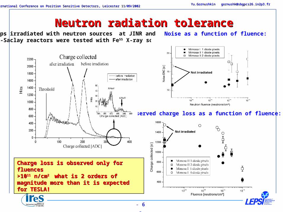
Neutron radiation toleranceNeutron radiation toleranceNoise as a function of fluence:
Observed charge loss as a function of fluence:
Charge loss is observed only for Charge loss is observed only for fluences fluences >10>101111 n/cm n/cm2 2 what is 2 orders of what is 2 orders of magnitude more than it is expected for magnitude more than it is expected for TESLA!TESLA!
Chips irradiated with neutron sources at JINR and CEA-Saclay reactors were tested with Fe55 X-ray source.

- 7 -
66thth International Conference on Position Sensitive Detectors International Conference on Position Sensitive Detectors ,, Leicester Leicester 1 111//0909/200/20022Yu.Gornushkin [email protected] [email protected]
MIMOSA 5: big chip - simple quick start MIMOSA 5: big chip - simple quick start solutionsolution
AMS 0.6 µm process with ~14 µm epitaxial layeranalogue readout - with hardware processing (CDS, pedestal subtraction,
S/N analysis, sparsification on-line) stitching: coarse - 100 µm + scribeline, option:precise – 1 m
Lot of 6”wafers 44 kEuro
19.4
mm
19.4
mm
17.35 mm
One chip ~10One chip ~1066 pixels of 17x17 pixels of 17x17 mm22
6
6

- 8 -
66thth International Conference on Position Sensitive Detectors International Conference on Position Sensitive Detectors ,, Leicester Leicester 1 111//0909/200/20022Yu.Gornushkin [email protected] [email protected]
MIMOSA-5 testsMIMOSA-5 tests
Titre :c1Auteur :ROOT Version 3.02/07Aperçu :Cette image EPS n'a pas été enregistréeavec un aperçu intégré.Commentaires :Cette image EPS peut être imprimée sur uneimprimante PostScript mais pas surun autre type d'imprimante.
Titre :c1Auteur :ROOT Version 3.02/07Aperçu :Cette image EPS n'a pas été enregistréeavec un aperçu intégré.Commentaires :Cette image EPS peut être imprimée sur uneimprimante PostScript mais pas surun autre type d'imprimante.
Titre :c1Auteur :ROOT Version 3.02/07Aperçu :Cette image EPS n'a pas été enregistréeavec un aperçu intégré.Commentaires :Cette image EPS peut être imprimée sur uneimprimante PostScript mais pas surun autre type d'imprimante.
The chip (4 matrices of 512512 pixels (17x17 m2 ) etched down to 120 m was exposed to 120 GeV/c - beam at CERN-SPS
The same process as MIMOSA-1 the same performances expected?
Preliminary results:Preliminary results: Noise mean ENC 20.7 eNoise mean ENC 20.7 e--
Seed pixel S/N 23Seed pixel S/N 23Detection efficiency Detection efficiency ~99.3%,~99.3%,spsp~1.7~1.7m,m,gaingain 2-3% 2-3%
close to those of MIMOSA-1close to those of MIMOSA-1
Titre :Main displayAuteur :ROOT Version 3.02/07Aperçu :Cette image EPS n'a pas été enregistréeavec un aperçu intégré.Commentaires :Cette image EPS peut être imprimée sur uneimprimante PostScript mais pas surun autre type d'imprimante.
Noise larger than in case of MIMOSA-1 (different serial r.o.architecture – double source follower stage)
Epitaxy layer ~14 m charge ~1000e-

- 9 -
66thth International Conference on Position Sensitive Detectors International Conference on Position Sensitive Detectors ,, Leicester Leicester 1 111//0909/200/20022Yu.Gornushkin [email protected] [email protected]
MIMOSA-5 response to inclined tracksMIMOSA-5 response to inclined tracks(very preliminary):(very preliminary):
Titre :c1_n7Auteur :ROOT Version 3.02/07Aperçu :Cette image EPS n'a pas été enregistréeavec un aperçu intégré.Commentaires :Cette image EPS peut être imprimée sur uneimprimante PostScript mais pas surun autre type d'imprimante.
Titre :c1Auteur :ROOT Version 3.02/07Aperçu :Cette image EPS n'a pas été enregistréeavec un aperçu intégré.Commentaires :Cette image EPS peut être imprimée sur uneimprimante PostScript mais pas surun autre type d'imprimante.
Total charge follows cos-1()
S/N grows as well (saturation observed due to geometrical effect at large angles)
MIMOSA-5 tests will MIMOSA-5 tests will continuecontinuein October 2002 at CERN-in October 2002 at CERN-PSPS

- 10 -
66thth International Conference on Position Sensitive Detectors International Conference on Position Sensitive Detectors ,, Leicester Leicester 1 111//0909/200/20022Yu.Gornushkin [email protected] [email protected]
MIMOSA-6 – first sensor with MIMOSA-6 – first sensor with integrated signal processingintegrated signal processing
0.35 MIETEC technology (same as MIMOSA-2)IReS-LEPSI/DAPNIA collaboration
•24 column readout in parallel•128 pixels per column•5MHz effective readout frequency (30MHz clock, 6 clock cycles/pixel)•Amplification (x5.5), Correlated Double Sampling on pixel•Discriminators integrated on chip periphery (1 per column)•Power dissipation ~500 mW per column
Pixel layout:28x28 m2
Chips are expected back from foundry this days.Chips are expected back from foundry this days.Test results - by the end of 2002.Test results - by the end of 2002.
Charge storagecapacitors
29 transitstors
AC
cou
plin
g ca
paci
tor
Matrix of 128x30 pixels
Discriminators
Chip layout:

- 11 -
66thth International Conference on Position Sensitive Detectors International Conference on Position Sensitive Detectors ,, Leicester Leicester 1 111//0909/200/20022Yu.Gornushkin [email protected] [email protected]
SummarySummary::
o The good performance of CMOS MAPS in charge particle detection has been succesfully established with 4 generations of small scale prototypes:
99%, sp~1.5-2.5 m, S/N~30, 2hit~30 mo Tolerance to neutrons exceeds TESLA requirements by
more than 2 orders of magnitude!o Preliminary results from MIMOSA-5 tests indicate that
these performances are reproducible with real size detectors
(~3.5 cm2, 120 m thin)o First chip with integrated signal processing functions
(CDS+A+D) is coming back from fabrication soon tests in October 2002
o R&D programme on CMOS MAPS TESLA Vertex Detector in a collaboration of 10 labs in F-UK-CH-NL-D+… is under way.


![[ Outline ]](https://static.fdocuments.us/doc/165x107/56815a74550346895dc7db61/-outline--56b49f971d862.jpg)


