Optical memory disks in optical information...
20
Optical memory disks in optical information processing Demetri Psaltis, Mark A. Neifeld, Alan Yamamura, and Seiji Kobayashi We describe the use of optical memory disks as elements in optical information processing architectures. The optical disk is an optical memory device with a storage capacity approaching 1010 bits which is naturally suited to parallel access. We discuss optical disk characteristics which are important in optical computing systems such as contrast, diffraction efficiency, and phase uniformity. We describe techniques for holographic storage on optical disks and present reconstructions of several types of computer-generated holograms. Various optical information processing architectures are described for applications such as database retrieval, neural network implementation, and image correlation. Selected systems are experimentally demonstrated. Key words: Optical memory disk, spatial light modulator, optical computing, computer-generated holo- grams. I. Introduction Ever since the introduction of the videodisc system in the late 1970s and the compact audio disk player in the mid-1980s, optical disk technology has been ma- turing at a rapid pace. Both write-once read-many (WORM) and magnetooptic read/write disk drives are presently available for high density storage on main- frames and personal computers. The conventional mode of both reading and writing used in present optical disk systems is serial. Specifically, a laser source will write one bit of data at a time on the disk, typically through a thermal mechanism.' Readout is achieved by using a lower power beam to illuminate the location of each bit on the disk individually and, based on the reflected or transmitted intensity detected, the bit is decoded as a logical 1 or 0. Although serial readout is well suited to conventional computers, the optical disk itself is naturally a parallel readout de- vice. 2 ' 3 To see this, consider illuminating a large por- tion of the disk with a collimated beam. The reflected or transmitted light contains all the data originally recorded in the illuminated area and a simple imaging system makes these data available to a detector array. This parallel access capability can be attractive when trying to solve memory access and contention prob- lems in parallel computing architectures or when try- Seiji Kobayashi is with Sony Corporation, Tokyo 100-31,Japan; the other authors are with the California Institute of Technology, Pasadena, California 91125. Received 17 July 1989. 0003-6935/90/142038-20$02.00/0. © 1990 Optical Society of America. ing to implement an intelligent memory search proce- dure as with database machines. 4 Further, the optical disk represents a high resolution, computer controlla- ble, spatial light modulator (SLM) which may be used in various optical computing architectures. For exam- ple, images stored on an optical disk may serve as a library of references in an optical image correlator and holograms stored on the disk may serve as interconnect patterns for hybrid optical/VLSI based neural net- works. In this paper we discuss the application of optical disk technology to areas in which parallel retrieval may be advantageous. We begin by characterizing the disk system used in our work, a Sony prototype sampled format drive with both WORM and magnetooptic me- dia. In Sec.III we discuss parallel optical readout of 2- D blocks of data such as images. In the same section, we describe the use of optical disks as holographic storage media. We present and analyze several tech- niques for storing and retrieving data holographically and suggest some applications of holographic disk based storage. In Sec. IV we describe the use of optical disks as both storage and interconnect elements in neural network architectures. Finally, optical disk based image correlators are described and demonstrat- ed in Sec. V. All the applications we discuss here are designed to combine the parallelism and interconnec- tivity of optics with a mature optical disk technology to result in feasible optical systems that perform useful computational tasks. II. Characterization The prototype Sony disk system used in most of our work (Fig. 1) can read and write both write-once and magnetooptic 5-in. reflective optical disks. The sys- tem records data as circular 1l-m diam pixels along a 2038 APPLIED OPTICS / Vol. 29, No. 14 / 10 May 1990
Transcript of Optical memory disks in optical information...

Optical memory disks in optical information processing
Demetri Psaltis, Mark A. Neifeld, Alan Yamamura, and Seiji Kobayashi
We describe the use of optical memory disks as elements in optical information processing architectures. Theoptical disk is an optical memory device with a storage capacity approaching 1010 bits which is naturally suitedto parallel access. We discuss optical disk characteristics which are important in optical computing systemssuch as contrast, diffraction efficiency, and phase uniformity. We describe techniques for holographicstorage on optical disks and present reconstructions of several types of computer-generated holograms.Various optical information processing architectures are described for applications such as database retrieval,neural network implementation, and image correlation. Selected systems are experimentally demonstrated.Key words: Optical memory disk, spatial light modulator, optical computing, computer-generated holo-grams.
I. Introduction
Ever since the introduction of the videodisc systemin the late 1970s and the compact audio disk player inthe mid-1980s, optical disk technology has been ma-turing at a rapid pace. Both write-once read-many(WORM) and magnetooptic read/write disk drives arepresently available for high density storage on main-frames and personal computers. The conventionalmode of both reading and writing used in presentoptical disk systems is serial. Specifically, a lasersource will write one bit of data at a time on the disk,typically through a thermal mechanism.' Readout isachieved by using a lower power beam to illuminate thelocation of each bit on the disk individually and, basedon the reflected or transmitted intensity detected, thebit is decoded as a logical 1 or 0. Although serialreadout is well suited to conventional computers, theoptical disk itself is naturally a parallel readout de-vice.2'3 To see this, consider illuminating a large por-tion of the disk with a collimated beam. The reflectedor transmitted light contains all the data originallyrecorded in the illuminated area and a simple imagingsystem makes these data available to a detector array.This parallel access capability can be attractive whentrying to solve memory access and contention prob-lems in parallel computing architectures or when try-
Seiji Kobayashi is with Sony Corporation, Tokyo 100-31, Japan;the other authors are with the California Institute of Technology,Pasadena, California 91125.
Received 17 July 1989.0003-6935/90/142038-20$02.00/0.© 1990 Optical Society of America.
ing to implement an intelligent memory search proce-dure as with database machines.4 Further, the opticaldisk represents a high resolution, computer controlla-ble, spatial light modulator (SLM) which may be usedin various optical computing architectures. For exam-ple, images stored on an optical disk may serve as alibrary of references in an optical image correlator andholograms stored on the disk may serve as interconnectpatterns for hybrid optical/VLSI based neural net-works.
In this paper we discuss the application of opticaldisk technology to areas in which parallel retrieval maybe advantageous. We begin by characterizing the disksystem used in our work, a Sony prototype sampledformat drive with both WORM and magnetooptic me-dia. In Sec. III we discuss parallel optical readout of 2-D blocks of data such as images. In the same section,we describe the use of optical disks as holographicstorage media. We present and analyze several tech-niques for storing and retrieving data holographicallyand suggest some applications of holographic diskbased storage. In Sec. IV we describe the use of opticaldisks as both storage and interconnect elements inneural network architectures. Finally, optical diskbased image correlators are described and demonstrat-ed in Sec. V. All the applications we discuss here aredesigned to combine the parallelism and interconnec-tivity of optics with a mature optical disk technology toresult in feasible optical systems that perform usefulcomputational tasks.
II. Characterization
The prototype Sony disk system used in most of ourwork (Fig. 1) can read and write both write-once andmagnetooptic 5-in. reflective optical disks. The sys-tem records data as circular 1l-m diam pixels along a
2038 APPLIED OPTICS / Vol. 29, No. 14 / 10 May 1990

Fig. 1. Sony prototype optical disk system.
spiral on the disk with 20,000 turns between a 3-cminner radius and 6-cm outer radius. The disk is divid-ed into thirty-two sectors, and each loop of the spiralfrom the beginning of sector 0 to the end of sector 31 iscalled a track. Because the radius of the trackschanges gradually with angle, we often model thetracks as concentric circles separated by 1.5 ,m. Pix-els are recorded with a constant angular separation of.001°. This corresponds to an along track pixel-to-pixel separation that varies between .5 Asm and 1 mdepending on radial position on the disk. This pixelrecording density yields a storage capacity of over 7 X109 bits on each side of the disk. The system is inter-faced to a personal computer (PC) which providesserial read/write access to the disks. The system canread or write up to 15 million bits/s. Consequently a1000 X 1000 image can be entered on the disk in 1/15 s.Since we can only write one line of the image perrevolution, about 30s are required to record the imagein 2-D format on the disk. Note, however, that athousand images using the same tracks could also bewritten during the same amount of time.
A variety of materials and recording mechanismshave been proposed for use in optical disks.' Webriefly describe the recording mechanism employed inthe write-once disk that we use in our experiments (seeRef. 5 for further details). The disk contains four thinmetal alloy films of Sb2 Se3 (300 A), Bi2Te3 (150 A),Sb2 Se3 (1400 A), and Al (1000 A) formed by sputteringdeposition on a glass or plastic substrate. The thick-ness of the various layers is chosen so that they form alow (5%) reflectivity interference filter. During therecording stage, a focused laser beam heats a spot ofthe Bi2Te3 layer through absorption. The Bi2Te3 andSb 2Se3 then form a four-element alloy by diffusion,eliminating the sharp interfaces between the layers.The low reflectivity interference filter is thus de-stroyed increasing the reflectivity of the medium to12%. This reflectivity difference is detected during
readout and decoded as a logical 1 or 0. The reflectiv-ity of an interference filter is wavelength dependent.Our quoted figures are for the 633 nm He-Ne illumina-tion that we use, but the thicknesses of the layers arechosen to maximize the change in reflectivity for thelaser diode wavelength of 830 nm.
The magnetooptic disk contains a rare earth transi-tion-metal alloy of TbFeCo. During the recordingstage, the laser heats a spot on the disk above 1800C,the Curie temperature of the material. As the spotcools below this temperature, the material within thespot retains the magnetization of an external fieldapplied perpendicular to the disk surface. The polar-ization of a low power readout laser rotates on reflec-tion from the spot by an angle of ±0.150, from themagnetooptic Kerr effect. The reflectivity of themagnetooptic disk is 17%, and the sign of the rotationangle depends on the direction of magnetization in thespot. This rotation is detected through a crossed po-larizer and decoded as a logical 1 or 0. Depending onthe setting of the polarizers, the amplitude of the lightcorresponding to the two states can be either on/off orplus/minus.6
Current disk systems use either continuous or sam-pled format schemes to maintain the position of thehead over data in a track. Continuous format systemsuse a return signal either from a guide-groove em-bossed on the disk or the recorded data itself to con-stantly monitor and correct the position of the headrelative to the data in a track. In contrast, sampledformat systems, such as our experimental one, usetracking and timing information embossed along radi-al lines on the disk to periodically monitor and correctthe head position. These lines of tracking and timinginformation appear every 270 pixels. Each line con-sists of a pattern of three embossed pits repeated in all20,000 tracks as shown in Fig. 2. The first two pitsprovide tracking information. They are displaced anequal distance from the center of the track, one toward
10 May 1990 / Vol. 29, No. 14 / APPLIED OPTICS 2039

Tmr In g
T r- o. c kC I| I gDo.to.
Fig. 2. Sampled-format tracking and timing information system.
the inside of the disk and the other toward the outside.If the head is exactly over the center of the track, thereadout signal strength of the two pits will be equal;otherwise, the signal returning from one of the pits willbe stronger than the other, thus indicating the direc-tion to move the head. The third pit provides timinginformation used to synchronize the system clock andthe disk.
There are two byproducts of the sampled formatscheme that facilitate the parallel readout of data.First, the across track alignment of tracking and tim-ing information combined with the synchronizationbetween recorder and disk rotation allows us to specifythe position of individual pixels with submicron accu-racy in any one of more than one billion locations.This provides us with across track coherence, the abili-ty to radially align pixels across different tracks. Incontrast, with continuous format systems, the positionof pixels in different tracks can drift by several pixelwidths within a single sector. Second, the absence ofguide-grooves allows us to retrieve high contrast im-ages from low contrast media through schlieren imag-ing as described in Sec. III.
When we consider using the disk as a spatial lightmodulator, a number of additional performance issuesarise. The resolution is determined by the track spac-ing in the radial direction (1.5 gtm) and the minimumspot size in the azimuthal direction (0.5-1 Em). No-tice that there is an inherent sampling in the radialdirection due to the tracks. At the outer tracks, wherethe recorded pixels do not overlap, the image is alsosampled in the azimuthal direction. We see later thatwe can make use of image diffraction caused by thissampling. Figure 3 shows the far field diffractionpattern when a grating recorded on the disk is illumi-nated. The grating was formed by periodically record-ing two tracks with all pixels on followed by two trackswith all pixels off. In Fig. 3(a), the grating is recordedon the inner tracks where pixels overlap along thetrack. In this case, the image is sampled in only onedimension thus producing diffraction orders in onedimension only. Figure 3(b) shows the diffractionwith the same grating recorded at the outer edge of thedisk. In this case, sampling in both dimensions resultsin a 2-D diffraction pattern. The maximum spatialfrequency that can be recorded without aliasing of theimage spectra is one-half of the sampling frequency ineach direction.
(a)
(b)
Fig. 3. Far field diffraction pattern from grating: (a) grating writ-ten on inner tracks (R = 3 cm); and (b) grating written on outer
tracks (R = 6 cm).
The reflectance function of the disk is basically bi-nary both for the write-once and the magnetoopticdisks. We have observed some dynamic range in thereflectivity of the write-once disks, controllable byvarying the exposure for each pixel. We have not yetcharacterized fully the grey scale capability of the sys-tem. In any case, some form of area modulation can beused to encode multiple grey levels at the expense ofspace-bandwidth product. We will demonstrate onesuch method in the following section. The contrast ofthe light reflected from the disk is low for the Sonywrite-once disks (2:1). For magnetooptic disks, thepolarization of the modulated light is orthogonal to thepolarization of the incident light and the use of orthog-onal polarizers in conjunction with the carrier encod-ing method discussed in the next section yields excel-lent contrast, limited primarily by the quality of thepolarizers.
2040 APPLIED OPTICS / Vol. 29, No. 14 / 10 May 1990

R
Y
6
Fig. 5. Coordinate system for calculating the effect of track curva-ture.
5mm
Fig. 4. Interferogram of Sony WORM disk.
Many of the processing architectures we propose usecoherent processing techniques requiring phase uni-formity across the surface of the disk. We have used aFizeau interferometer to measure the phase uniformi-ty of the Sony disks. Figure 4 shows a Fizeau interfer-ogram of a 24- X 36-mm area of a glass-covered Sonywrite-once disk taken with a He-Ne laser source pro-viding illumination. The figure shows numerous re-gions on the disk with optical thickness variations ofless than a wavelength ( = 633 nm) over distances ofseveral millimeters. These regions are sufficientlylarge to contain images or holograms thousands ofpixels on a side. The greater phase variation towardsthe outer edge of the disk is most likely caused by indexvariations due to stresses induced during manufactur-ing. We have also tested plastic-covered disks whichgenerally show greater phase variation than the glass-covered ones.
In most uses, it would be more convenient if theoptical disk system recorded pixels on a Cartesian grid.However, as noted earlier, our system actually writespixels along curved tracks. We can neglect this curva-ture if we restrict attention to a small area of the disk.Consider a region at a distance R from the disk center.As shown in Fig. 5, we establish Cartesian coordinateaxes with x in the azimuthal or along track directionand y in the radial or across track direction. Equation(1) converts the polar coordinates of the disk to theCartesian coordinates in the region of interest:
x = r sin(O) (1)r cos(()(-R1The center-to-center spacing of the pixels in the radialdimension is 3r and the angular separation betweenadjacent pixels is 6 in azimuth. We now superimposea Cartesian grid on this pixel structure with x and yspacings as follows:
Ax = 1 (2)
This choice for A., and Ay provides the best matchbetween the pixels recorded on the disk and the pointson the Cartesian grid. We now calculate the deviationof the pixel locations from their presumed Cartesianlocations. The presumed coordinates of the points onthe Cartesian grid are
Ix':= nAx
-y MA4J(3)
whereas the actual location of the pixels on the polargrid are
[r= R+ Mbr + 2° Br2ar
= J~ (4)
The actual Cartesian coordinates of the recorded pix-els, therefore, are
x = (R + mr + n 2 r) sin(nl0) n + nm X AY
1 ( R + 6 ~ o a r\~M rA + A A A 2| (R +Mr 2 n cos(no) -R -- m4 + n x4 _ n2 ___ |V ~~ m ~ + 2 /o ,m n 2rR 2R
(5)
We calculate the deviation between the actual pixelposition and the presumed location on the Cartesiangrid by subtracting Eq. (5) from Eq. (3):
|f = x-x MU nm ~'x4A - x-l Yxtnm 2 R R
I 2rR 2R~27rR2RJ(6)
For an array of 1000 X 1000 pixels on the Sony disks,the worst case pixel placement error is 1.25% of thearray size (12.5 pixels) in the x-direction (at R = 3 cm,Ax = 0.5 Am, and Ay = 1.5 Am) and 0.14% of the arraysize (1.4 pixels) in the y-direction (at R = 6 cm, Ax = 1,m, and Ay = 1.5 ym). In applications where this kindof positional error is not tolerable, we need to compen-sate the curvature through optical techniques and/orthe recording geometry. We describe such methods ingreater detail in the following section.
Diffraction efficiency is a key parameter in deter-mining overall system efficiency since many of the
10 May 1990 / Vol. 29, No. 14 / APPLIED OPTICS 2041
Inner Edge Outer Edge

optical systems presented in the following sections uselight diffracted from the disk. Given an accuratemodel of the surface reflectivity of the disk and how itwill be used in an optical system, we can calculate theexpected efficiency of the disk in that application. Wemodel the reflectivity pattern of the disk using thefollowing equation:
r(xy) = r + (r, -r) [abnm(x - nA,,y - mAy)] 0 s(xy), (7)n,m
where bnm represents the binary pixel pattern, ro and r,the reflectivity of unwritten and written pixels, respec-tively, the convolution operation, and s(x,y) theshape of each pixel.
The light reflected from the surface of the diskEr(X,Y) is the product of the reflectivity pattern of Eq.(7) with the field of the illuminating light beam E(x,y):
Er(x,y) = Ej(xy)r(xy). (8)
We can use Fresnel diffraction to calculate the fielddue to light reflected from the disk at any distancefrom the disk, as follows:
E(xyz) = JEr(x',Y,) z exp(Jkl) dx'dy', (9)f f ~jXl212 = (X -x') 2 + (y _ y) 2 + 2. (10)
The efficiency X of the disk can then be found byintegrating the intensity of light reflected by the diskover the region of space z where the optical systemcaptures reflected light and dividing by the incidentlight energy:
JJJ IE(xy,z)i2 dxdydz
I1 =
J f JE(Xy)12dxdy
In the Appendix, as an example, we estimate the dif-fraction efficiency of the disk for schlieren imaging ofthe first diffracted order. Substituting parameters forthe Sony write-once disk into Eq. (A7), [r 12 = 0.12,IroI2 = 0.05, Ax = 0.5 Am, = 1.5 Am, and Ar = 0.5 Amwith b(xy) = 1, n = 0, and m = 1], we find an estimatedefficiency of Be = 0.112% compared with a measuredefficiency of flm = 0.114%. We estimate that the mag-netooptic disk will be almost 1000X less efficient thanthe write-once disk in most applications. This largeloss in efficiency was also observed experimentally.
III. Imaging and Holography
The fact that data can be retrieved in parallel fromoptical disks creates the possibility for eliminatingsome of the bottlenecks that currently exist in comput-ers due to the mismatch between mass storage mediaand semiconductor memories.2 A parallel random ac-cess memory would be one possible way to construct aparallel readout optical memory. In this case, M outof the N bits stored on a disk could be specified andretrieved simultaneously. In such a system, the appa-ratus that would scan the memory to realize this paral-
Fig. 6. Photograph of image written on Sony WORM disk.
lel retrieval capability would have to be set in (N) (NIM)M distinct states to arbitrarily select any M-tuple.With N = 1010 and M = 1000, we obtain about 107000distinct states. It is clearly not practical to realize anoptical scanning mechanism that can do this. There-fore, we conclude that we must somehow structure thestored data to reduce the complexity of the accessmechanism. The most straightforward way to imposesuch structure is to arrange the stored data in 2-Dblocks, M bits each, that are retrievable in parallel.This reduces the number of choices the access mecha-nism addresses to a practical (NIM) = 107 for thepreviously quoted numbers. In this section, we dis-cuss several methods, including holographic, for re-cording and retrieving 2-D blocks of data from opticaldisks.
Figure 6 is a photograph of a binary image written onthe Sony write-once disk as viewed through a micro-scope. This image consists of 4024 X 512 pixels re-corded on a polar grid. Note that the track curvatureis not visible. The parallel lines, evident in the figure,are the radial strips of tracking and timing informationdescribed in the previous section. There are 270 pixelsbetween each pair of these lines. Individual pixels arenot discernible in this figure, but they are perfectlyaligned in the radial direction resulting in the accuraterecording of the letters in the figure. Note the poorcontrast in Fig. 6. This is because the disk has an off-state (unwritten) reflectivity of 5%, while the on-state(written) reflectivity is only 12%. This large back-ground and low differential reflectivity results in thepoor contrast seen in the photo. Rilum and Tanguayused an interferometric technique to eliminate thebackground light obtained on reflection from astamped optical disk.7 This technique is not applica-ble to the Sony disk because the recorded data do notappear as embossed pits but rather as local variationsin surface reflectivity. We use an alternative meansfor improving the contrast of the retrieved image.Since the binary image b(xy) to be recorded on thedisk is sampled by a polar grid, light reflected from thedisk will be diffracted into many orders or sidebandswhose center frequencies will be determined by the
2042 APPLIED OPTICS / Vol. 29, No. 14 / 10 May 1990

grid spacing. To make this clear, consider Eq. (12) forthe reflectivity of the disk:
r(xy) = r + (r, - r) [b(xy) t(x - nAx,y - mA)] s(xy),n,m
(12)
with the x-axis in the along track direction and the y-axis in the radial direction, as before. Since the back-ground reflectivity r is not sampled, energy in thefirst- and high-order diffracted fields arises only fromthe presence of the recorded image. Therefore, animage formed by the first-order diffracted field will notcontain any bias light and will have high contrast. Wecan calculate how much energy is diffracted into thefirst-order and compare this to the total incident ener-gy to obtain an estimate for the efficiency of the disk.The Fourier transform of the reflectivity function is
R(u,v) r(uv) + (r, - r)
X [(UMv 0 A E 6( _ n , vn )] S(u v), (13
where B(u,v) and S(u,v) are the Fourier transforms ofb(x,y) and s(x,y), respectively.
The term that contributes to the formation of thedesired image is
Ri(u,v) = B uv - -) S(u,v). (14)
From these two equations we can express the diskefficiency as
= f f IRi(u,v)1Pdudv. (15)
For the Sony optical disk we have calculated the diskefficiency to be 0.112% (see Sec. II for parameters).This value agrees well with the measured efficiency of0.114%. For a more detailed derivation of the efficien-cy of a schlieren imaging system used to image theoptical disk surface, see the Appendix. An example ofa high contrast image obtained by imaging the firstdiffracted order is shown in Fig. 7. The light diffract-ed by the tracks was selected to form this image.
As described in Sec. II, when we assume that pixelsare written on a Cartesian grid, the presence of trackcurvature leads to positional errors given by Eq. (6).In the schlieren imaging system described above, thepositional error of a recorded spot can lead to ampli-tude and phase errors in its contribution to the reflect-ed field. We neglect the amplitude error since it onlybecomes significant when the position error (x,y) iscomparable to the distance between the disk and theimage plane. The phase error observed in a givendirection, however, can be approximated in most casesby the dot product between the wavevector in thatdirection k and the position error. Since Iki is large,this phase error cannot be neglected. When we con-sider only the first-order diffracted beam, kx = 0 andthe apparent phase error over the disk is given by
Perr(XY;) = k * (Xy) = k x2 (16)
Fig. 7. High contrast image obtained by imaging the first-orderdiffracted component of light reflected by the disk used in Fig. 1.
If= -R kky
2 for the +1 order,
ky = -Ay2 for the -1 order.
AY
(17)
(18)
This phase error can be modeled as a cylindrical lens atthe disk plane with focal length f = Ry/X. Fortypical experimental parameters R = 4.5 cm, Ay = 1.5Asm, and X = 633 nm, the cylindrical focal length is 10.7cm. This distortion can be corrected by an illumina-tion system containing a cylindrical lens of focal lengthF. The product of the incident wavefront and thereflectance function of the disk in this case is
E,(x,y) = Ej(xy)P(xy), (19)
where Er(xy) is the reflected field, Ei(xy) = exp(jax 2)is the incident field corrected by the cylindrical lens,and (x,y) is the apparent reflectance function of thedisk surface including the phase error. The illuminat-ing optics should be chosen so that Er(x,y) = r(xy),which yields a = -k/2f. With this value for a, theincident illumination is given by Ei = exp(-jkx 2 /2f)which can be generated by a line source located adistance f in front of the disk. A cylindrical lens withfocal length F, at a distance F + f in front of the disk,can be used to form the line source.
Correcting for this cylindrical lens effect does not,however, account for the positional errors of pixels dueto the polar grid. In Sec. II we found that the positionerror of pixels in large images can exceed the pixelspacing. Since some applications require pixel posi-tion errors less than the interpixel separation, to mini-mize these errors we must make the interface to thedisk conform to this polar recording format. For ex-ample, to accurately record an image sensed by a tele-vision camera, the camera should be modified to scanalong curved lines matching the shape of the tracks onthe disk.
Although the optical disk is basically a binary stor-age medium, it can also encode grey level images. Areamodulation can be used to code multiple reflectivity
10 May 1990 / Vol. 29, No. 14 / APPLIED OPTICS 2043

Fig. 9. Reconstruction of a binary Fresnel hologram stored onoptical disk.
Fig. 8. Grey scale image written on optical disk using area modula-tion.
levels for superpixels consisting of several bits. Forexample, turning on n out of N pixels in a superpixelcan be used to represent the integer value n. Varioussuperpixel coding techniques have been investigatedin the past.8 We have implemented an area modula-tion scheme which uses a stochastic procedure to de-termine the position of on-pixel locations within eachsuperpixel. In addition, this scheme improves thedynamic range of regions of low spatial frequency bystochastically selecting the value to be recorded in eachelement of an array of superpixels. Specifically, if auniform region of p superpixels maps to a grey levelbetween n and n + 1, randomly choosing between twolevels for each superpixel in the region provides theentire p-superpixel region with an expected grey levelequal to any one of p - 1 additional levels between nand n + 1. Figure 8 was generated using the areamodulation recording scheme on the write-once diskand a schlieren imaging system as described above.The image shown consists of 512 X 480 superpixelseach of dimension 6 X 4 pixels. The number of dis-tinct grey levels recorded on the disk therefore wastwenty-five. The grey levels present in the originalimage are clearly evident in the figure.
In addition to the recording and retrieval of images,the optical disk is an ideal medium for the storage ofcomputer generated holograms (CGHs).9-12 25 Theimaging technique described above may be thought ofas simply the reconstruction of an image plane holo-gram. Any other computer generated hologram canjust as easily be stored on the optical disk. We haveinvestigated various techniques for the calculation andrecording of CGHs on the optical disk.
The first method we investigated is based on usingthe computer to form the holograms of the individualpoints that make up an image. Thresholding a Fresnel
hologram of a single point (xojyo,zo) yields a Fresnelzone plate. It can be calculated by simply evaluatingthe real part of the Fresnel transform of a single pointand thresholding the result, as shown below:
hp(xy) c sgn [Re {JJ OX' - -
X exp(j AZ) [(x' - x) 2 + (y' - Y)2Idx'dy'}]P (20)
oc sgn [cos (Az [(x - Xo)2 + (Y - yo)21)] (21)
The reconstruction of the object point is achieved byilluminating the reflection hologram hp(x,y) with aplane wave. One component of the reflected field is aspherical wave converging to the point (x0,y0 ,z0). In asimilar fashion, the Fresnel hologram of multiplepoints is calculated by summing many individual holo-grams and thresholding the result:
h(x,y) = sgn [ cos( 7 [(x - Xm)2 + (Y - Ym)2) (22)
where (xm,ym,zm) are the coordinates of the dots withwhich we construct the image that is stored holograph-ically. The Ym terms are chosen in the range from 0 toXzo/;A-T _X2 , and the xm terms in the range from 0 toXzo/TA. - X2. This guarantees that the reconstructionof the first-order in the y-direction does not overlapwith any of the other orders. In effect, this is how weconstruct an off-axis hologram. If the number of dotsthat comprise the image is far less than the space-bandwidth product of the hologram, a reconstructionwith high signal-to-noise ratio (SNR) is obtained.
Figure 9 shows the reconstruction of a binary Fres-nel hologram we have recorded on a write-once disk.The reconstructed object contains over 100 points.The hologram consists of a 1000 X 1000 array of pixelsrecorded on the disk at a radius equal to 4 cm. Bysimply illuminating the hologram with a raw beam, weobserve a self-focused reconstruction at a distance of10 cm from the disk. The size of the reconstructedimage is 3 X 5 cm which is much larger than the size of
2044 APPLIED OPTICS / Vol. 29, No. 14 / 10 May 1990

Fig. 10. Reconstruction of Fresnel hologram stored on magnetoop-tic disk.
the hologram itself (0.7 X 1 mm). This is a convenientfeature which allows us to match the high densitystorage medium with a lower resolution array of detec-tors. Figure 10 shows the reconstruction of a Fresnelhologram recorded on the magnetooptic disk. In thiscase, the reconstructed hologram was observedthrough crossed polarizers to enhance the contrast.This polarization filtering technique, made possible bythe polarization switching property of magnetoopticmodulation, is necessary in this case because of thelower efficiency of the magnetooptic disk.
We can also record any conventional CGH (e.g.,Lohmann or Lee).' 3 -'5 One CGH technique we haveinvestigated consists of forming 1-D superpixels withposition encoding of phase information. As can beseen in Fig. 11(a), each 1-D superpixel consists of fourpixels along a specific track. By selecting the appro-priate combinations of pixels to record within a group,each superpixel can be made to represent any of thenine phasors including the zero phaser shown in Fig.11(b). We may also be able to represent a largernumber of phasors without increasing the size of thesuperpixels by varying the size of the recorded pixels.In our system, this can be accomplished by eitherchanging the energy used to write each pixel or bymultiply exposing pixels.
We can also store Fourier holograms by simply re-cording the complex Fourier transform of the objectfield as described above. The Fourier transform holo-gram can be calculated in a number of ways; for exam-
Fig. 12. Reconstruction of Fourier transform hologram.
ple, we could use the fast Fourier transform algorithmor we could calculate a Fresnel hologram using Eq. (22)with a large z0. This latter approach is equivalent tocalculating the Fraunhofer diffraction pattern of theobject and is the approach we have chosen. Shown inFig. 12 is the reconstruction from a binary Fouriertransform hologram. The data for this hologram werecomputed by thresholding the real part of the Fouriertransform of the object. The hologram consists of1000 X 1000 pixels written on the disk at a radius of 4cm. Reconstruction was achieved using a Fouriertransform lens.
One can also combine the Fourier and Fresnel holo-gram methods described above. For example, Fig. 13shows the image reconstructed from a hologram gener-ated using the Fourier transform in the along trackdirection and the Fresnel hologram in the across trackdirection. This transformation is given by the follow-ing equation:
Track direction
000O
.Re
000[a] [b]
Fig. 11. Schematic of CGH technique used to re-cord complex valued pixels: (a) one-dimensionalsuperpixel used to code phase information; and (b)
complex values recordable using (a).
10 May 1990 / Vol. 29, No. 14 / APPLIED OPTICS 2045

resolution element in the reconstruction from an N. XNy-pixel Fourier transform hologram is given by
{; =AXF
A.,N
(24)
in the x- and y-directions, respectively. F is the focallength of the Fourier transform lens used in the recon-struction.
The shift observed in the reconstruction plane as afunction of disk rotation angle 0 is
Fig. 13. Reconstruction of Fourier along track/Fresnel across trackhologram.
__ = :Wtikyn- = f(_)
Fig. 14. Multilayer feedforward neural network.
h(xy) J J b(x',y') exp[j Liz (y - yt)2J exp( L xx')dy'-
(23)
As before, we record a thresholded version of the realpart of h(xy). Reconstruction is achieved using acylindrical lens. Another storage scheme might in-volve calculating the 1-D Fourier transform of eachline of the object and storing these 1-D signals alongseparate tracks. One benefit of using the Fouriertransform in the along track direction and an imaginglens across track is that across track coherence is nolonger required for parallel readout of 2-D data arrayssince each track reconstructs a shift invariant line ofdata.'6
We would also like to use the shift invariance proper-ty of the Fourier holograms in the along track directionto generate stationary reconstructions from a rotatingdisk. Unfortunately, this is not exactly true. As thedisk rotates, the hologram experiences both transla-tion and rotation. Rotation of a Fourier transformhologram results in an equal rotation of the reconstruc-tion around the axis defined by the direction of thezero-order reflected beam. Thus, disk rotation resultsin apparent rotation and translation of the recon-structed image. We can neglect this motion if thereconstructed image moves less than a resolution ele-ment during the observation period. The size of a
I.e,(0) =XF [cos(O) - 112A (
-yo =2sin(O) II~, A(25)
The hologram subtends an angle = NA. In orderthat the reconstruction remain stationary during arotation of the disk by 0, we find the following limits onthe size of the hologram:
Ny<AYeY(O)
Maki g asmal 0 ppro imaion we rri e atthefol(26)
Making a small 0 approximation, we arrive at the fol-lowing set of constraints for N, and Ny:
i. (27)
Thus, for the disk parameters in our experiment, theholograms must be smaller than 300 X 300 pixels, if werequire the motion of the reconstruction to be negligi-ble.
IV. Neural Networks
Neural network architectures are particularly wellsuited for the use of optical disks. This is due to thelarge memory that is typically required for the storageof the interconnecting weights in large networks. Theoptical disk not only supplies this storage capability,but in addition it provides the rapid access that isnecessary for fast computation of the mapping of thenetwork. Figure 14 shows a multilayer feedforwardnetwork, the most common neural network architec-ture. In this architecture, neurons are grouped inlayers. The input to the jth neuron in the lth layer is xland its output is y(. The weight of the interconnectionbetween the input of this neuron and the output of thekth neuron in the previous layer is Wlk. Equation (28)governs the operation of the networ:
(28)1 ~ = W Y 1 }
= f(xW)
where f is typically a sigmoidal function.
2046 APPLIED OPTICS / Vol. 29, No. 14 / 10 May 1990

Disk
SynapsesFig. 16. Schematic of VLSI neural network crossbar implementa-
tion.
Fig. 15. Optical disk/VLSI hybrid neural network implementation.
An implementation of a feedforward network usingoptical disks combined with analog VLSI chips isshown in Fig. 15. The VLSI chip implements a singlelayer of the network. The weights that are used forpropagating through one layer are optically loaded viathe third dimension from the disk. An array of photo-diodes is integrated into the VLSI chip for this pur-pose. The weights for the different layers of the net-work are stored adjacent to one another along theazimuthal direction of the disk. To achieve a multi-layer network, we first download the weights for thefirst layer. The VLSI chip then evaluates the responseof the first layer and stores the result. Meanwhile, thedisk is spun so that the weights of the next layer arealigned with the chip, the new weights are downloadedand the response for the next layer is evaluated on thechip. This procedure is repeated until the response ofthe final layer is evaluated.
There are several possible implementations of thebasic idea described in the previous paragraph. Wedescribe a particular chip design which we are im-plementing experimentally. A schematic diagram ofthis chip is shown in Fig. 16. The neurons and syn-apses are arranged as a crossbar. The output of eachneuron in the top row is a voltage source that raises thepotential of its corresponding vertical wire to 5 V ifthe neuron is on or sets it to 0 V if the neuron is off.The amount of current that flows from each verti-cal wire into a horizontal wire is determined by thechannel resistance of the field effect transister FET atthe corresponding intersection. The total current ineach horizontal wire is the sum of the currents thatwere contributed from all the vertical wires. Thissummed current becomes the input to the neuron at-tached to each horizontal line. The neuron circuitaccepts the input current, thresholds it, and generatesan output voltage. The entire circuit is actually bidi-rectional. A horizontal wire that was previously used
to sum the currents that flow from the vertical wires,can also be used to broadcast the state (voltage) of theneuron attached to it. Consequently, if the weightscan be dynamically updated, a single chip can be usedfor the implementation of a multilayer network withdata going back and forth between the two sets ofneurons.
The strength of the connection between two neuronsis increased by raising the gate voltage of the FETlocated at the intersection between the correspondingwires. The gate voltage is controlled by a circuit con-sisting of a series combination of a reverse-biased pho-todiode and a second, reset transistor. At the begin-ning of each cycle, the reset transistors are turned on,which sets the gates of the synapse transistors to 0 V.The reset transistors are then turned off for the rest ofthe cycle. The weights that are stored on the disk areimaged onto the chip. To facilitate this description,we will assume for the moment that the weights arebinary (0,1) and we discuss later in more detail how tohandle multivalued weights. When light from thedisk strikes a photodiode on the chip, current flowsthrough the photodiode charging the gate of the syn-apse transistor. This turns the transistor on, allowingcurrent to flow between horizontal and vertical wires.We have not yet completed the testing of this chip, butwe have characterized a circuit that consists of just twosynapses that are however much more complex.
Figure 17 is a circuit diagram of one of the synapsesthat were fabricated. This synapse is a multiplyingdigital-to-analog converter (MDAC)17 contributing acurrent to the target neuron proportional to the prod-uct between the signal received from the input neuronand the weight, encoded as a binary quintuple, that isoptically received by a set of five photodiodes. Theweight and the neuron activity can be bipolar. This isachieved through the use of a pair of horizontal andvertical wires for each neuron. We denote the wires inthe vertical and horizontal directions by V+,V; and
10 May 1990 / Vol. 29, No. 14 / APPLIED OPTICS 2047

v Vm
Fig. 17. Synapse circuit diagram.
Fig. 18. Photograph of MDAC synapses.
H+,H-, respectively. Four of the five photodiodes arededicated to receiving the four bit weight value and thefifth, on the far left of Fig. 17, is for the sign bit. Thefive reset transistors in this design initially charge thegate voltages of the synapse transistors to Vdd. Thereare two pairs of pass transistors shown in Fig. 17. Atany one time, one transistor of each pair is on and theother is off. In this manner, the setting of the passtransistors determines which two perpendicular wiresare connected. The setting of the pass transistors iscontrolled by the sign bit with the help of the invertercircuit. The strength of the interconnection is deter-mined by the setting of the synapse transistor, which inturn is determined by the optical signal on the photo-diodes (the binary encoded weight). The channel re-sistance of an FET is proportional to its width-to-
length ratio (W/L). The analog-to-digital conversionis performed by scaling logarithmically W/L in the foursynapse transistors. For example, suppose we are re-ceiving a positive input signal along the vertical wiresand the weight is negative. In this case, both verticalwires are set to 5 V by the output stage of the associatedneuron. The sign bit through the pass transistorscloses the circuit between the V- and Hn wires. Theamount of current that flows to Hn is proportional tothe integer value corresponding to the four bit binarynumber detected by the photodiodes and also dependson the voltage setting (Vref • 5 V) of Hn-. If the sign bitflips, current will flow in the same direction but on H+.The target neuron subtracts the currents on Hn+ andHn to form its output and hence a bipolar weight isrealized.
2048 APPLIED OPTICS / Vol. 29, No. 14 / 10 May 1990
Vm_' V' Em
Photodiodes

The photograph in Fig. 18 shows the pair of synapseswhich was fabricated through MOSIS. The circuitryfor the synapses is protected by a layer of metal. Eachof the ten squares in the figure containing r shapedfeatures is a 26- X 27-Asm opening in this protectivelayer which allows light to strike the 20- X 21-jumphotodiode located underneath. The plot of Fig. 19shows the current on H vs Vref for voltages of 5 V(neuron on) and 0 V (neuron off) on V+. When Vref isset to 0 V (5 V), the resulting current swings between 0,gA (-140 isA) and 140 JLA (0 uA). In other words,when Vref is set to either 0 V or 5 V, this is a two-quadrant multiplier. If, however, Vref is set to anyintermediate value, the output current swing is bipo-lar. In particular, for the circuit we fabricated, whenVref = 1.17 V, the positive and negative deviations ofthe current are symmetric and we have a balancedfour-quadrant multiplier.
The speed of the neural network chip is limitedprincipally by the time required to discharge the gatesof the synapse transistors through the photodiodes.The discharge current depends on the amount of lightstriking it and the voltage across the photodiode. Fig-ure 20 shows the current flowing though the synapse asa function of time as all the photodiodes are simulta-neously struck with light for three different intensitylevels; Vref was set to 1.17 V for this measurement. Asexpected, the response time is inversely proportionalto the light intensity and corresponds to a switchingenergy of 1.55 pJ. This chip was not optimized forspeed (phototransistors could be used in place of thephotodiodes); however, we can use the measurement ofFig. 20 to obtain an estimate for the speed with whichwe can operate such a network. Let us assume that wehave available optical power equal to 1 W and a chipconsisting of 100 X 100 synapses. The diffractionefficiency of the disk was estimated to be approximate-ly 0.1% which yields 1 mW total power incident on thechip, or 100 nW per synapse. Dividing the switchingenergy by the available power per synapse, we obtain15.5 us response time. This corresponds to 3 Gbits/stransfer rate between memory and chip. Even thoughthis is a remarkable rate, there is a lot of room forimprovement in the speed in this design, through adisk with better light efficiency, the use of phototran-sistors, and a reduction in the number of bits used inthe MDACs.
In the neural network implementation describedabove, the disk is used only as a parallel read-outstorage device and the electronic chip is used to per-form all the calculations. It is also possible to use thedisks as computer-generated holograms or transparen-cies in many of the optical neural network architec-tures that have been previously proposed.'8 In suchoptical neural networks, the analog multiplicationneeded to implement the weights is performed bypropagating an incident light field through a transpar-ency (the disk in this case) and summing multiple suchproducts onto a single detector location. To accom-plish this, the output of each neuron must be an opticalsignal. This can be done through the use of spatial
1.5
1.0*
0.5
¶Z
6~V
-0.5
-1.0-
-1.5-
Synapse Current vs Vref
Vi. = 5V
Vref (V)
Fig. 19. Synapse current dependence on Vref.
100
.
1.
a.a3
0
36.4pW/cm 2
10 Time(ms)
Fig. 20. Synaptic time response dependence on light intensity.
HolographicOpticalElements onDisk
Neurons withSources andDetectors
Fig. 21. Optical disk implementation of synaptic connections.
light modulators or optoelectronics. The optoelec-tronic approach for building the neurons combinedwith implementation of the synapses on the disk isschematically shown in Fig. 21. The neurons can befabricated in GaAs'9 on which detectors, sources, andelectronic circuits can be monolithically integrated.We can greatly increase the density of neurons on theGaAs chip compared to the previous approach, sincewe no longer require circuitry on the chip to detect theweights and multiply them with the neuron outputs.Second, since optics provides us with greater flexibilityin performing the interconnections between the neu-
10 May 1990 / Vol. 29, No. 14 / APPLIED OPTICS 2049
5s

rons, we can, at least in principle, construct not onlylarger but also more general neural network architec-tures beyond multilayer feedforward networks.
V. Correlators
The correlation function c(i,y) is defined as
c(ij) = 9-'JF(wsw)G*(wxw,)}
= f f f(x,y)g(x - gy - )dxdy,
(29)
(30)
where f(x,y) and g(x,y) are two real images, F(wx,wY)and G(wxwy) are their respective 2-D Fourier trans-forms, and Sol'{ is the 2-D inverse Fourier transformoperator. It is well known that c(i,y) is sharplypeaked at the point (xo,yo) when f(xy) = g(x - x0,y -yo). This property is what makes the correlation func-tion useful for pattern recognition because, regardlessof the position of the input image g(x,y), c(i,5) willhave a peak if f(xy) and g(x,y) are matched. Since, ingeneral, there are many versions of an image g that wewould like to recognize, a reliable image recognitionsystem should provide invariance to multiple objectattributes. Often the best way to achieve this invari-ance is to use a large number of reference patterns fagainst which to compare g in order to obtain reliablerecognition.
Optical image correlators based on Fourier trans-form (FT) holograms were proposed by VanderLugt in1964.20 For optical correlation to be a realistic ap-proach to image recognition, we require a memorydevice sufficient to store a large reference image li-brary, an SLM which interfaces with this memory inreal time, and a scanning or addressing mechanismwhich allows interrogation of the entire reference li-brary in a reasonable amount of time. The opticaldisk provides these three characteristics in one device.In this section, we describe several optical disk basedimage correlation architectures and present experi-mental results taken from selected systems.21 22 Wewill examine critical parameters associated with eacharchitecture and evaluate each system in terms of pow-er and speed.
A. VanderLugt CGH Correlator
The first disk based image correlator to be describedis the simple VanderLugt correlator shown in Fig. 22.As can be seen from the figure, a Fourier transformcomputer-generated hologram recorded on the opticaldisk is used as a Fourier plane filter for the inputimage. The product of the transforms of the input andreference images is formed at the disk and an inversetransform yields the desired 2-D correlation in theoutput plane. As the disk rotates, a new correlationpattern is generated every time a different CGH alignswith the input image FT. Therefore, whenever thereis a match between the input FT and the CGH, a peakoccurs in the output plane of the system. The locationof this peak, which corresponds to the location of theobject of interest in the input plane, may be anywherein the correlation plane. Therefore, a 2-D detectorarray is required to acquire the correlation data. Fur-
CORRELATIONPLANE I /
I -4' 4'
5 L+ _< - INPUT
I I PLANE
\ I\ I\ I\ I
CG
OPTICALDISK
Fig. 22. Optical disk based VanderLugt correlator.
thermore, since the correct correlation only occurs dur-ing the brief periods of alignment between the inputFT and the CGH, the detector array need only bequeried at these times. A pulsed laser or an electroni-cally gated detector array could be used to achieve theappropriate sampling. The proper operation of thissystem depends on the optical quality of various diskcoating materials which are capable of introducingrandom phase distortions across the system filterplane. As we discussed in Sec. II, however, the opticalquality of several commercially available disks is suffi-cient to make them suitable for these applications.
As with other FT based architectures, one advantageof this correlator is its potentially high speed. Thecorrelation rate in this system is limited by disk rota-tion rate and detectability of the correlation peak.Taking a typical disk rotation rate of 40 Hz, we calcu-late a correlation rate R, = 400,000 correlations/s for100 X 100 pixel images. This correlation rate impliesthat to detect a correlation peak, each element of the2-D detector array in the output plane must have abandwidth of 400 kHz. Further, we can calculatethe peak detectibility np given by the number of pho-tons detected at the correlation peak, by first calculat-ing the peak dwell time r, multiplying this by theexpected power in the correlation peak Pc, and divid-ing by the photon energy. That is:
np = rPIhv, (31)
where v is the frequency of the optical field. Peakdwell time is given simply by - = 1/NRC where N is thenumber of pixels in the reference image in the alongtrack direction. In the case of random, bipolar images,the expected fraction of diffracted power that will bemeasured at the peak is 1/2. By random we mean thateach pixel of the image is equally likely to take oneither of the two possible values ±1. Given the diskdiffraction efficiency, a, and the source power P8, thecorrelation peak power is
P = nP/2. (32)
Substituting P = 10 mW and = 0.1%, we find anexpected peak power P = 5 W. This rate leads to an
2050 APPLIED OPTICS / Vol. 29, No. 14 / 10 May 1990
e_

easily detectable 105 photons in the correlation peak.The two most significant drawbacks of this system arealignment criticality and computational overhead.For each reference filter, a 2-D FT CGH must becomputed and written on the disk. For a large refer-ence library the time required for this procedure can belong. More importantly, the alignment of the inputFT and the CGH is critical to within the resolution ofthe CGH ( 1 m). As the disk rotates, nonuniformi-ties resulting from wobble and disk center offset, leadto nonuniformities in reference image location withrespect to the optical system. For example, the SonyWORM disks we use allow up to 10 of wobble and up to50 /im offset between the rotational center of the diskand the actual track center. These nonuniformitiesmust be compensated for the output correlation to beaccurate.
B. Photorefractive Correlator
Since the wobble and offset problems introduceslowly varying nonuniformities (<50 wobble cycles/rotation), the problem of alignment sensitivity can beeffectively dealt with using real time compensationwith feedback of the sort used in commercial diskdrives; however, the computational overhead associat-ed with generating the desired reference library in theabove system remains a problem. The system of Fig-ure 23 eliminates this processing time by allowing thereference images themselves to be recorded on the diskinstead of FT CGHs. In this system, a photorefractivecrystal or any other real time, temporary holographicstorage medium is used to record a hologram of theinput FT. During the recording phase, the disk illu-mination is blocked and the input transparency is illu-minated from the right. A hologram is formed be-tween the input FT and the reference beam as shown.This hologram will then be read out using the referencelibrary. On readout, the input is blocked and the diskis illuminated. The product of the input and referenceFTs is formed in the crystal and inverse transformed toyield the correlation output.
If the photorefractive crystal is replaced by a thinmedium such as a holographic plate, then the outputpattern is exactly the desired 2-D correlation; however,it has been shown that when a thick hologram is used inthe filter plane of such a system, the resulting output isa 1-D slice of the 2-D correlation pattern.23 This canbe understood by considering the recording arrange-ment shown in Fig. 23. On recording, each plane wavecorresponding to one of the points in the input imageforms a grating with the reference beam. The result-ing hologram exhibits Bragg selectivity in the horizon-tal direction. On readout, a point along a given radialline on the disk can only read out those gratings formedby points along one vertical line in the input. Eachsuch line on the disk reads out a corresponding array ofholograms and generates a vertical array of spots in thecorrelation plane at the horizontal location corre-sponding to the reference beam FT. The coherentsum of all such reconstructions comprises the output ofthe correlator. This output pattern is the desired 2-D
Referen
Photorefractive Crystal ofrelation Plane
/ ~~~L2
-e Beam
XC] 'Lr> lA
Disk
Input Plane
Optical Disk
Fig. 23. Photorefractive/optical disk based correlator.
correlation multiplied, in the horizontal direction, by asinc function whose width is inversely proportional tothe hologram thickness. In the system of Fig. 23, thisproperty does not cause problems since all 1-D slicesare obtained sequentially via disk rotation. Further,instead of requiring a full 2-D detector array at theoutput, a 1-D array is sufficient to sequentially detecteach slice of correlation output. Despite the advan-tages gained in terms of computational overhead anddetector simplicity, alignment compensation remainsa critical issue with this system. The expected correla-tion rate obtainable using this system is again limitedprimarily by disk speed and peak detectability. A rateof 400,000 correlations/s is still easily achievable,yielding a detected signal at the correlation peak ofmore than 105 photons using again a 10 mW source.
This system has been experimentally demonstratedusing a thin hologram in place of the photorefractivecrystal. For this experiment, we chose to use a SonyWORM disk as an SLM at the input as well as thereference. The results are shown in Fig. 24. Figure24(a) shows the image recorded on two Sony disks; onedisk was used to record the filter plane hologram on theplate and the another was used to read out the holo-gram. The correlation plane output is shown in Fig.24(b). The characteristic autocorrelation peak ap-pears in the output.
C. Rotating Mirror Correlator
The previous two Fourier transform based correla-tors implement Eq. (29) to generate the correlationfunction. While FT based systems are typically supe-rior in terms of speed, alignment and coherence re-quirements are relative disadvantages. We discussnext two systems which perform 2-D correlationsbased on Eq. (30). In these systems the correlationfunction is generated by calculating an inner productfor every relative shift between input and reference
10 May 1990 / Vol. 29, No. 14 / APPLIED OPTICS 2051
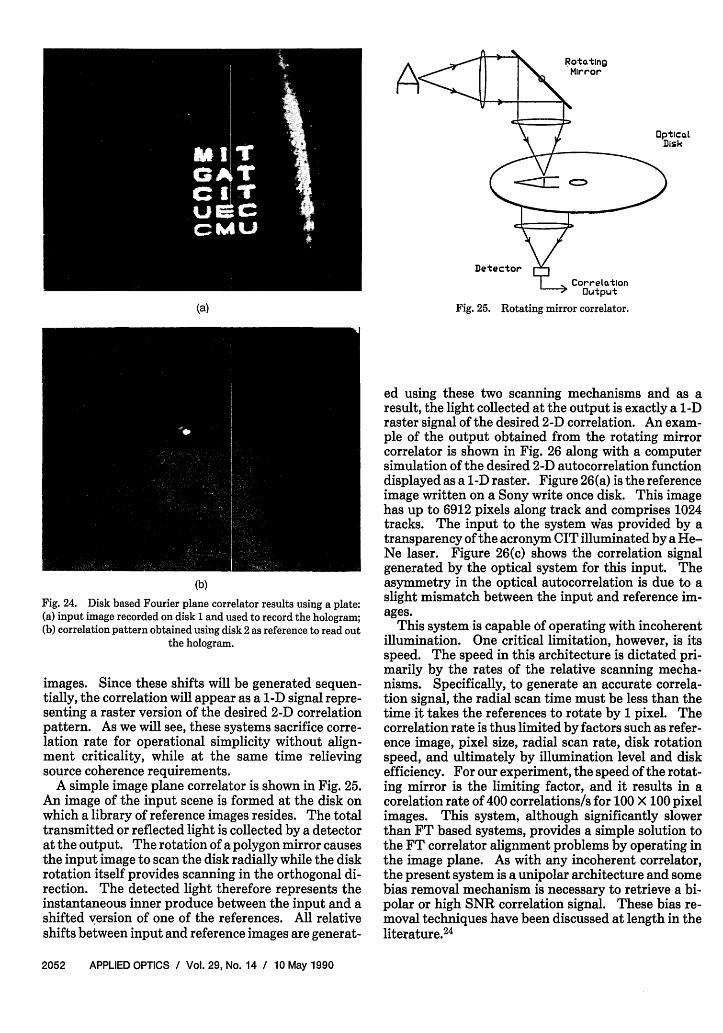
RotatingMirror
(a)
(b)
Fig. 24. Disk based Fourier plane correlator results using a plate:(a) input image recorded on disk 1 and used to record the hologram;(b) correlation pattern obtained using disk 2 as reference to read out
the hologram.
images. Since these shifts will be generated sequen-tially, the correlation will appear as a 1-D signal repre-senting a raster version of the desired 2-D correlationpattern. As we will see, these systems sacrifice corre-lation rate for operational simplicity without align-ment criticality, while at the same time relievingsource coherence requirements.
A simple image plane correlator is shown in Fig. 25.An image of the input scene is formed at the disk onwhich a library of reference images resides. The totaltransmitted or reflected light is collected by a detectorat the output. The rotation of a polygon mirror causesthe input image to scan the disk radially while the diskrotation itself provides scanning in the orthogonal di-rection. The detected light therefore represents theinstantaneous inner produce between the input and ashifted version of one of the references. All relativeshifts between input and reference images are generat-
\ 1 ~~~~OpticalA ft ~~~~~~~Dsk
DetectorCorrelation
Output
Fig. 25. Rotating mirror correlator.
ed using these two scanning mechanisms and as aresult, the light collected at the output is exactly a 1-Draster signal of the desired 2-D correlation. An exam-ple of the output obtained from the rotating mirrorcorrelator is shown in Fig. 26 along with a computersimulation of the desired 2-D autocorrelation functiondisplayed as a 1-D raster. Figure 26(a) is the referenceimage written on a Sony write once disk. This imagehas up to 6912 pixels along track and comprises 1024tracks. The input to the system was provided by atransparency of the acronym CIT illuminated by a He-Ne laser. Figure 26(c) shows the correlation signalgenerated by the optical system for this input. Theasymmetry in the optical autocorrelation is due to aslight mismatch between the input and reference im-ages.
This system is capable of operating with incoherentillumination. One critical limitation, however, is itsspeed. The speed in this architecture is dictated pri-marily by the rates of the relative scanning mecha-nisms. Specifically, to generate an accurate correla-tion signal, the radial scan time must be less than thetime it takes the references to rotate by 1 pixel. Thecorrelation rate is thus limited by factors such as refer-ence image, pixel size, radial scan rate, disk rotationspeed, and ultimately by illumination level and diskefficiency. For our experiment, the speed of the rotat-ing mirror is the limiting factor, and it results in acorelation rate of 400 correlations/s for 100 X 100 pixelimages. This system, although significantly slowerthan FT based systems, provides a simple solution tothe FT correlator alignment problems by operating inthe image plane. As with any incoherent correlator,the present system is a unipolar architecture and somebias removal mechanism is necessary to retrieve a bi-polar or high SNR correlation signal. These bias re-moval techniques have been discussed at length in theliterature.24
2052 APPLIED OPTICS / Vol. 29, No. 14 / 10 May 1990

D. Acoustooptic Correlator
The most obvious way to improve the speed of theabove system is to increase the speed of the radialscanning mechanism. Since the speed of commercial-ly available polygon mirror based scanners is limited toabout 40 kHz, we have considered instead the systemof Fig. 27 which utilizes an acoustooptic (AO) device asthe radial scanner. The AO scanner can achieve scanrates up to 10 MHz. In this architecture, a chirp signalpropagating in the AO device generates a moving cylin-drical lens with power in the horizontal dimension.This moving cylindrical lens becomes part of the sys-tem that images the input onto the disk. Consequent-ly, as the AO lens moves horizontally, the imageformed on the disk is scanned radially. The orthogo-nal scanning is achieved by disk rotation as before andthe light collected by the detector once again repre-sents the desired correlation signal.
The correlation rate in this system is still con-strained by the radial scan speed; however, since thisscanning is generated by virtue of the propagation of aRF chirp in the Bragg cell, the resulting correlationrate is much higher than before. The RF chirp param-eters are chosen so as to utilize as much AO space-bandwidth product as the input image requires, whileminimizing scan time. Specifically,
tC = tAO(SBPIN/SBPAO), (33)
(b)
(c)
Fig. 26. Rotating mirror correlator results: (a) reference imagerecorded on Sony disk; (b) computer-generated autocorrelation sig-
nal; and (c) optical system output.
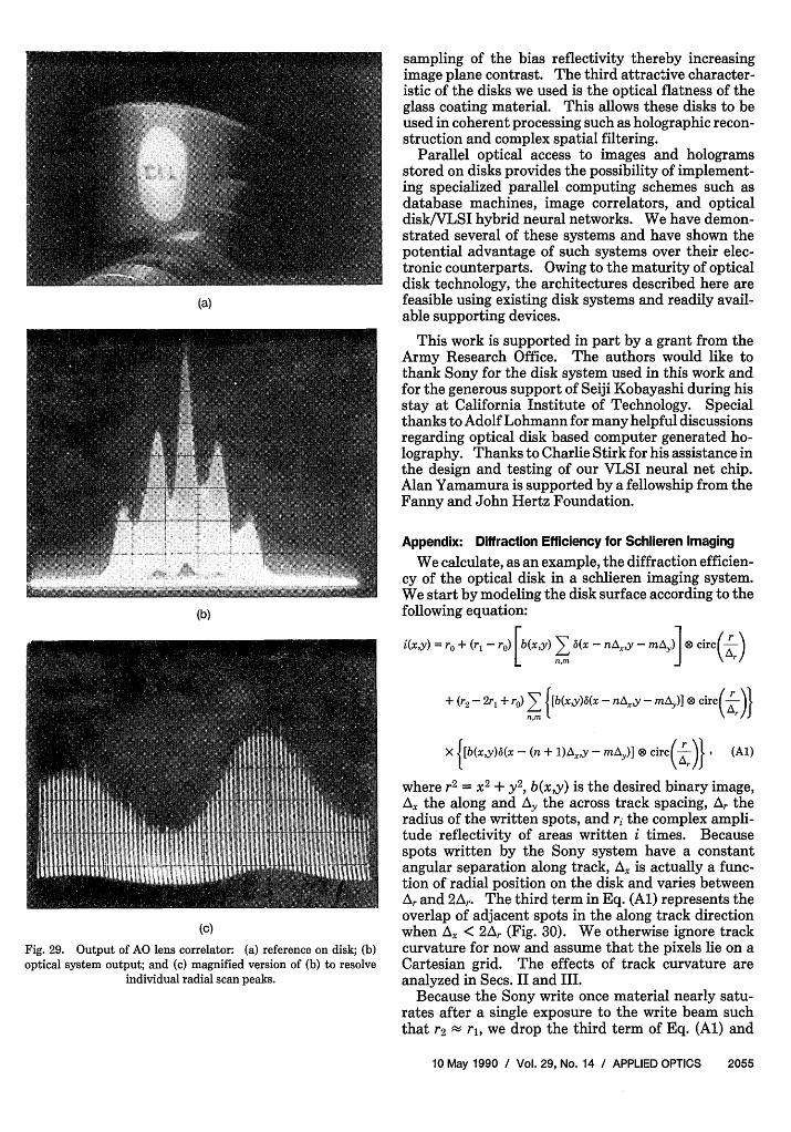
where tc is the required RF chirp duration, tAO is theAO aperture, and SBPIN and SBPAO are the input andAO space-bandwidth products, respectively. Wehave built this system using a TeO2 AO cell with a 70 ,saperture and a RF chirp centered at 40 MHz with achirp rate of 4 MHz/As. Using the above equationwith SBPIN = 100 and SBPAO = 1000 the requiredchirp duration was calculated to be 7 irs. A SAWdevice was used to generate the desired chirp signal.The resulting radial scan rate of 1/7 As 140 kHz,yields a correlation rate of 1400 correlations/s. Again,this correlator is incoherent, but quasimonochromaticlight would be required because of the wavelengthsensitivity of the AO lens. The impulse response ofthe AO lens scanner is shown in Fig. 28. The image ofan input transparency was formed on a CCD using onecylindrical lens with power in the horizontal dimensionand the AO lens for vertical imaging. The input illu-mination was pulsed so that the AO lens might befrozen in various vertical positions. The delay be-tween the onset of the RF chirp and the laser diodepulse determines the position of the image on the CCD.As can be seen from the figure, the AO lens imagingcharacteristics are quite good. The output of the AOlens correlator is shown in Fig. 29. The input to thissystem was once again the transparency of the acro-nym CIT and the reference was a duplicate CIT writ-ten on an Optotech WORM disk using a simple record-ing system which we built. The correlator output is,therefore, the 2-D autocorrelation of the input image.The reference image shown in Fig. 29(a) is relativelylarge so that a radial scanning distance of 2 cm was
10 May 1990 / Vol. 29, No. 14 / APPLIED OPTICS 2053
(a)

Input Plane
Uptical Disk
2-D Correlaion OutputDetector
Fig. 27. Moving AO lens correlator.
CHIRPGm1ERATOR
CCD
LIJ
(a) (C)
(b) (d)
Fig. 28. Impulse response of the AO lens scanner: (a) opticalsystem used to measure impulse response; (b)-(d) image formed onCCD for various delay times A, where A is the time between theleftmost edge of the chirp gate (upper trace) and the laser diode
trigger (lower trace), (b) A = 2.5jus, (c) A = 5.0,us, (d) A = 8.0 ps.
required to generate an accurate correlation signal. ingsystems. ThelargeSBP(-101),simplecomputerAs can be seen from Figs. 29(b) and 29(c), the optical addressability, natural scanning mechanism, and par-system output agrees well with the predicted autocor- allel accessibility are all features making the opticalrelation signal of Figure 26(b). disk a candidate for use as both memory and SLM in
these systems. The sampled format recording schemeVI. Conclusions results in across track coherence, facilitating the stor-
This paper describes the use of optical memory disks age of 2-D data on the disk. This format also results inin optical computing and optical information process- the absence of grooves on the disk, which eliminates
2054 APPLIED OPTICS / Vol. 29, No. 14 / 10 May 1990
sampling of the bias reflectivity thereby increasingimage plane contrast. The third attractive character-istic of the disks we used is the optical flatness of theglass coating material. This allows these disks to beused in coherent processing such as holographic recon-struction and complex spatial filtering.
Parallel optical access to images and hologramsstored on disks provides the possibility of implement-ing specialized parallel computing schemes such asdatabase machines, image correlators, and opticaldisk/VLSI hybrid neural networks. We have demon-strated several of these systems and have shown thepotential advantage of such systems over their elec-tronic counterparts. Owing to the maturity of opticaldisk technology, the architectures described here arefeasible using existing disk systems and readily avail-able supporting devices.
This work is supported in part by a grant from theArmy Research Office. The authors would like tothank Sony for the disk system used in this work andfor the generous support of Seiji Kobayashi during hisstay at California Institute of Technology. Specialthanks to Adolf Lohmann for many helpful discussionsregarding optical disk based computer generated ho-lography. Thanks to Charlie Stirk for his assistance inthe design and testing of our VLSI neural net chip.Alan Yamamura is supported by a fellowship from theFanny and John Hertz Foundation.
Appendix: Diffraction Efficiency for Schlieren Imaging
We calculate, as an example, the diffraction efficien-cy of the optical disk in a schlieren imaging system.We start by modeling the disk surface according to thefollowing equation:
i(x,y) = ro + (r - ro) [b(xy) B(x- ny - mAY)] ® circ(\ r)
+ (r2- 2r, + r0) {[b(x~y)(x - nAxy -m)] circ( r)}
X {[b(x,y)6(x - (n + l)A,,y - mA) circ( )}, (Al)
(c)
Fig. 29. Output of AO lens correlator: (a) reference on disk; (b)optical system output; and (c) magnified version of (b) to resolve
individual radial scan peaks.
where r2 = x 2 + y 2, b(x,y) is the desired binary image,Ax the along and Ay the across track spacing, Ar theradius of the written spots, and ri the complex ampli-tude reflectivity of areas written i times. Becausespots written by the Sony system have a constantangular separation along track, Ax is actually a func-tion of radial position on the disk and varies betweenAr and 24r. The third term in Eq. (Al) represents theoverlap of adjacent spots in the along track directionwhen Ax < 2r (Fig. 30). We otherwise ignore trackcurvature for now and assume that the pixels lie on aCartesian grid. The effects of track curvature areanalyzed in Secs. II and III.
Because the Sony write once material nearly satu-rates after a single exposure to the write beam suchthat r2 rl, we drop the third term of Eq. (Al) and
10 May 1990 / Vol. 29, No. 14 / APPLIED OPTICS 2055
(a)
(b)

account instead for the overlap by modifying the spotshape in the second term by assigning half of the over-lap region to each neighboring spot, as in Fig. 30. Inthis case, the mathematical expression for the spotbecomes [circ X rect] and Eq. (Al) reduces to thefollowing:
i(x,y) = r + (r1 - r) [b(xy) Ox - nAxy - mAY)]n,m
0 [circ(y-) rect(I)]- (A2)
H2A, -A
X cr r/ r
circ(r/A, )
Fig. 30. Model of spot shapes.
Strictly speaking, the above equation models the re-flectivity incorrectly wherever a written spot is adja-cent along track to an unwritten one. Assuming, how-ever, that along track spatial frequencies in the imageare low compared to the sampling frequency A-', weexpect separate clusters of written and unwrittenspots, in which case there would be little energy in aterm accounting for written spots next to unwrittenones.
Using Eq. (A2) to model the reflectivity of the disksurface, we find the following Fraunhofer diffractionpattern:
I(u,v) = rob(u,v) + (r, - r) [B(Uv) AA Eu v ]-
X [Ar Jl(2rArP) ® Ax sinc(Axu)6(v)]J 2 = 2 2 (A3)
As expected, the sampling in the image plane corre-sponds to convolving the image spectrum with an arrayof impulses resulting in an array of image spectra ordiffraction of the image into multiple orders. Schlie-ren imaging achieves high contrast because the pixelssample only the image and not the background, repre-sented by ro, sending all the energy in the bias to thezero-order.
The fraction of incident light that goes into then,mth diffraction order is given by integrating themagnitude squared of the appropriate term from Eq.(A3) as follows:
Hm = Ar(rr o) 2 n vA A J= J - -
The remaining integral corresponds to the energy inthe spectrum of the image which is equivalent to theenergy in the image itself. Thus, the fraction of inci-dent light energy that goes into the n,mth diffractionorder is given as follows:
r 1-r 0 2 IX An r Ao 2 I b(xy)12 dxdy
|ArJ,(27rArP) 2Xic/X~(~l~/b~/ x rI(2 P p 0 A., sinc(Axu)5(v)Iun ~~/Y. (A6)
Defining useful light as the total energy going intoimage spectra of all orders, we estimate the light cap-tured by imaging a single order as a fraction of usefullight:
Hnm
Z Hntm,n',m'=-
Ar Jl(27r0P) A 4 sinc(Axu)b(v)p
2
)U=n/A,,v=m/A4(A7)
J|(2irArP) 21Ar 0 Ax sinc(Axu)6(v) I~'A~~'A
Since the denominator is the sum of the squares ofthe Fourier series coefficients of an image with everyspot written with unity amplitude, it is equivalent tothe fraction of the disk covered by spots if all werewritten. This fraction varies between 0.877 at theinnermost radius and 0.785 at the outermost. We cannow simplify Eq. (A7) as follows:
X [ P) 0 Ax sinc(Axu)6(v)] 2 dudv. (A4) Hnm
J|(27rArP) 21Ar 0 A., sinc(A.Lu)6(v) Iun/Ax,vm/A
The shape of the written spots determines the char-acteristic [J1 @ (sinc X 6)] envelope which modulatesthe entire diffraction pattern in Eq. (A3). Assumingthat the pixels sufficiently oversample the input im-age, the envelope is nearly constant over the imagespectrum allowing us to simplify Eq. (A4):
|(r1 - ro) 2X JXl' n ,V M m) 12d
X rJi(27ArP)2X Ar P 0 Ax sinc(Au)a(v) u*n/tvm/Ai . (A5)
p nAmy
A /2 fAY/2 /r / X 12 dXdy
Z HnIf A \ A Jx /2 J- 2 circ )r rect )
(A8)
Ji(2irArP) 2Ar 0 A. sinc(Axu)6(v)
A sin- 1 A +
(A9)
Thus, Eq. (A6) shows the amount of light as a frac-tion of incident light that goes into the image spectrum
2056 APPLIED OPTICS / Vol. 29, No. 14 / 10 May 1990
circ(r/A,)rect(x/Ae)

in each order. Equation (A9) shows the amount ofimage light in each order as a fraction of image light inall orders. These equations can be used to estimatethe diffraction efficiency of the Sony write-once disk ina schlieren imaging system. The disk diffraction effi-ciency for other applications and/or disks can be esti-mated in a similar fashion given a model for the reflec-tion or transmission pattern of the disk andparameters for the appropriate disk characteristics.
References
1. R. Bartolini, H. Weakliem, and B. Williams, "Review and Analy-sis of Optical Recording Media," Opt. Eng. 15, 99-108 (1976).
2. Y. Abu-Mostafa and D. Psaltis, "Optical Neural Computers,"Sci. Am. 255, 88-95 (1987).
3. D. Psaltis, A. A. Yamamura, M. A. Neifeld, and S. Kobayashi,"Parallel Readout of Optical Disks," in Technical Digest, Topi-cal Meeting on Optical Computing (Optical Society of America,Washington, DC, 1989), pp. 58-61.
4. L. Giles and B. K. Jenkins, "Models of Parallel Computation and
Optical Computing," in Technical Digest, OSA Annual Meet-ing (Optical Society of America, Washington, DC, 1986), paperML1.
5. Y. Nakane et al., "Principle of Laser Recording Mechanism byForming an Alloy in the Multilayer of Thin Metallic Films,"Proc. Soc. Photo-Opt. Instrum. Eng. 529, 76-81 (1985).
6. D. Psaltis, E. G. Paek, and S. S. Venkatesh, "Optical ImageCorrelation with a Binary Spatial Light Modulator," Opt. Eng.23, 698-704 (1984).
7. J. H. Rilum and A. R. Tanguay, Jr., "Utilization of OpticalMemory Disks for Optical Information Processing," in Techni-cal Digest, OSA Annual Meeting (Optical Society of America,Washington, DC, 1988), paper M15.
8. J. F. Jarvis, C. N. Judice, and W. H. Ninke, "A Survey ofTechniques for the Display of Continuous Tone Pictures onBilevel Displays," Comput. Graphics Image Process. 5, 13-40(1976).
9. Y. Tsunoda, K. Tatsuno, K. Kataoka, and Y. Takeda, "Holo-graphic Video Disk: An Alternative Approach to Optical VideoDisks," Appl. Opt. 15, 1398-1403 (1976).
10. I. Satoh and M. Kato, "Holographic Disk Recording of DigitalData with Fringe Stabilization," Appl. Opt. 27, 2987-2992(1988).
11. T. Yatagai, J. G. Camacho-Basilio, and H. Onda, "Recording ofComputer-Generated Holograms on an Optical Disk Master,"Proc. Soc. Photo-Opt. Instrum. Eng. 1052, 119-124 (1989).
12. T. Inagaki, "Hologram Lenses Lead to Compact Scanners,"IEEE Spectrum 26, 39-43 (1989).
13. B. Brown and A. Lohmann, "Complex Spatial Filtering withBinary Masks," Appl. Opt. 5, 967-969 (1966).
14. W.-H. Lee, "Binary Computer Generated Holograms," Appl.Opt. 18, 3661-3669 (1979).
15. G. Tricoles, "Computer Generated Holograms: An HistoricalReview," Appl. Opt. 26, 4351-4360 (1987).
16. A. Lohmann, U. Erlangen-Nuremburg; personal communica-tion.
17. J. Alspector and R. B. Allen, "A Neuromorphic VLSI LearningSystem," Advanced Research in VLSI Processes 1987StanfordResearch Conference (MIT Press, Cambridge, 1987), pp. 313-349.
18. Special Issue on Neural Networks, Applied Optics 26, (1 Dec.1987).
19. J. H. Kim, S. H. Lin, J. Katz, and D. Psaltis, "MonolithicallyIntegrated 2-D Arrays of Optoelectronic Devices for NeuralNetwork Applications," Proc. Soc. Photo-Opt. Instrum. Eng.1043, 44-52 (1989).
20. A. VanderLugt, "Signal Detection by Complex Spatial Filter-ing," IEEE Trans. Inf. Theory IT-10, 139 (1964).
21. D. Psaltis, M. A. Neifeld, and A. A. Yamamura, "Optical DiskBased Correlation Architectures," in Technical Digest, TopicalMeeting on Optical Computing (Optical Society of America,Washington, DC, 1989), pp. 206-209.
22. D. Psaltis, M. A. Neifeld, and A. A. Yamamura, "Image Correla-tors Using Optical Memory Disks," Opt. Lett. 14, 429-431(1989).
23. J. Yu, "Optical Processing Using Photorefractive Crystals,"Ph.D. Thesis, California Institute of Technology (1988), Chap.5.
24. D. Psaltis, "Incoherent Electrooptic Image Correlator," Opt.Eng. 23, 12-15 (1984).
25. A. D. Mikaelyan, A. Vanin, E. D. Gulanyan, and S. Prokopenko,"Holographic Disk for Data Storage," Sov. J. Quantum Elec-tronics. 170(5), 680-687 (1987).
10 May 1990 / Vol. 29, No. 14 / APPLIED OPTICS 2057