On Logic Synthesis for Timing Speculation
6
On Logic Synthesis for Timing Speculation Yuxi Liu † , Rong Ye † , Feng Yuan † , Rakesh Kumar § and Qiang Xu † † CU hk RE liable Computing Laboratory (CURE) The Chinese University of Hong Kong, Shatin, N.T., Hong Kong Email: {yxliu, rye, fyuan, qxu}@cse.cuhk.edu.hk § Dept. of ECE, University of Illinois at Urbana-Champaign, USA Email: [email protected] ABSTRACT By allowing the occurrence of infrequent timing errors and correct- ing them with rollback mechanisms, the so-called timing speculation (TS) technique can significantly improve circuit energy-efficiency and hence has become one of the most promising solutions to mitigate the ever-increasing variation effects in nanometer technologies. As tim- ing error recovery incurs non-trivial performance/energy overhead, it is important to reshape the delay distribution of critical paths in timing- speculated circuits to minimize their timing error rates. Most existing TS optimization techniques achieve this objective with post-synthesis tech- niques such as gate sizing or body biasing. In this work, we propose to conduct logic synthesis for timing-speculated circuits from the ground up. Being able to manipulate circuit structures during logic optimiza- tion, the proposed solution is able to dramatically reduce circuit timing error rates and hence improve its throughput, as demonstrated with ex- perimental results on various benchmark circuits. 1. INTRODUCTION Technology scaling has brought various challenges to state-of-the-art integrated circuit (IC) design, among which the ever-increasing timing uncertainty caused by static and dynamic variation effects (e.g., man- ufacturing variability and runtime voltage/temperature fluctuations) is one of the most critical problems [1, 2]. To tolerate such timing uncer- tainty, conventional designs focus on worst-case parameters and rely on conservative design guardbanding to guarantee “always correct" opera- tions. Such worse-case-oriented design methodology, however, dramat- ically reduces the benefits brought by technology scaling. When there is no sufficient timing slack in a circuit, variation effects would manifest themselves as infrequent timing errors on its speed- paths [6, 7]. If we could detect the occurrence of timing errors and cor- rect them on-the-fly with little penalties, we can achieve error-resilient computing with improved circuit performance and/or energy-efficiency. Such “better-than-worst-case" design methodology has attracted lots of research attention from both academia and industry, and a number of so-called timing speculation (TS) techniques have been presented in the literature [3, 4, 5]. Since timing error detection and correction mechanisms are the en- abling techniques in timing-speculated circuit designs, there have been numerous research works to address these two issues. On one hand, many timing error detectors were presented in the literature (e.g., [8, 3, Permission to make digital or hard copies of all or part of this work for personal or classroom use is granted without fee provided that copies are not made or distributed for profit or commercial advantage and that copies bear this notice and the full citation on the first page. To copy otherwise, to republish, to post on servers or to redistribute to lists, requires prior specific permission and/or a fee. IEEE/ACM International Conference on Computer-Aided Design (ICCAD) 2012, November 5-8, 2012, San Jose, California, USA. Copyright c 2012 ACM 978-1-4503-1573-9/12/11 ...$15.00. 9]), among which Razor flip-flop [3] with double-sampling capability is the most representative one. On the other hand, timing error recovery is usually achieved by restoring system to a known-good pre-error state with microarchitectural-level support. For example, when a timing er- ror is detected in microprocessor datapath, the processor pipeline can be flushed. Then, by lowering the system frequency for a short period and replaying instructions, the processor is able to recover from the fail- ure cycle and continues its operations correctly with performance/power penalties paid for recovery and re-execution. Since the system operates at higher frequency without timing errors for the general case, the over- all system performance is expected to be improved, as long as timing errors do not occur frequently and the penalties paid to correct them are well controlled. Since timing error correction incurs non-trivial performance over- head, it is important to reduce the timing error probability of the circuit under a certain operational frequency to improve its throughput. Various techniques (e.g., [11, 12, 13, 14]) have been presented in the literature to achieve this objective, but most of them are conducted using post- synthesis optimization techniques such as gate sizing or body biasing. The effectiveness of these solutions is thus limited with fixed circuit structure at this stage. Motivated by the above, we propose to conduct logic synthesis for timing speculation from the ground up in this work. With the flexibility to manipulate circuit structural changes, our solution can dramatically improve the throughput of timing-speculated circuits, as demonstrated on various benchmark circuits. The main contributions of this work include: • We propose a simple yet effective model to estimate the impact of structural changes on the timing error probability of a circuit, by taking process variation effects and speed-path sensitization probability into consideration; • Using the proposed optimization metrics, we present novel logic synthesis techniques to improve the performance of timing-speculated circuits. The remainder of this paper is organized as follows. Section 2 presents the preliminaries of this work. In Section 3, we detail the proposed logic synthesis techniques for timing speculation. Experimental results on various benchmark circuits are then presented in Section 4. Finally, Section 5 concludes this paper. 2. PRELIMINARIES 2.1 Timing Speculation By detecting timing errors on-the-fly and conducting rollback error recovery, the circuit’s throughput and/or energy consumption can be sig- nificantly improved with timing speculation technique. One of the most representative solutions is the so-called Razor technique [3], wherein double-sampling sequential elements are used for timing error detection while counterflow pipelining technique [10] is used for error recovery. 591
Transcript of On Logic Synthesis for Timing Speculation

On Logic Synthesis for Timing Speculation
Yuxi Liu†, Rong Ye†, Feng Yuan†, Rakesh Kumar§ and Qiang Xu†
†CUhk REliable Computing Laboratory (CURE)The Chinese University of Hong Kong, Shatin, N.T., Hong Kong
Email: {yxliu, rye, fyuan, qxu}@cse.cuhk.edu.hk
§Dept. of ECE, University of Illinois at Urbana-Champaign, USAEmail: [email protected]
ABSTRACTBy allowing the occurrence of infrequent timing errors and correct-ing them with rollback mechanisms, the so-called timing speculation(TS) technique can significantly improve circuit energy-efficiency andhence has become one of the most promising solutions to mitigate theever-increasing variation effects in nanometer technologies. As tim-ing error recovery incurs non-trivial performance/energy overhead, itis important to reshape the delay distribution of critical paths in timing-speculated circuits to minimize their timing error rates. Most existing TSoptimization techniques achieve this objective with post-synthesis tech-niques such as gate sizing or body biasing. In this work, we propose toconduct logic synthesis for timing-speculated circuits from the groundup. Being able to manipulate circuit structures during logic optimiza-tion, the proposed solution is able to dramatically reduce circuit timingerror rates and hence improve its throughput, as demonstrated with ex-perimental results on various benchmark circuits.
1. INTRODUCTIONTechnology scaling has brought various challenges to state-of-the-art
integrated circuit (IC) design, among which the ever-increasing timinguncertainty caused by static and dynamic variation effects (e.g., man-ufacturing variability and runtime voltage/temperature fluctuations) isone of the most critical problems [1, 2]. To tolerate such timing uncer-tainty, conventional designs focus on worst-case parameters and rely onconservative design guardbanding to guarantee “always correct" opera-tions. Such worse-case-oriented design methodology, however, dramat-ically reduces the benefits brought by technology scaling.
When there is no sufficient timing slack in a circuit, variation effectswould manifest themselves as infrequent timing errors on its speed-paths [6, 7]. If we could detect the occurrence of timing errors and cor-rect them on-the-fly with little penalties, we can achieve error-resilientcomputing with improved circuit performance and/or energy-efficiency.Such “better-than-worst-case" design methodology has attracted lots ofresearch attention from both academia and industry, and a number ofso-called timing speculation (TS) techniques have been presented in theliterature [3, 4, 5].
Since timing error detection and correction mechanisms are the en-abling techniques in timing-speculated circuit designs, there have beennumerous research works to address these two issues. On one hand,many timing error detectors were presented in the literature (e.g., [8, 3,
Permission to make digital or hard copies of all or part of this work forpersonal or classroom use is granted without fee provided that copies arenot made or distributed for profit or commercial advantage and that copiesbear this notice and the full citation on the first page. To copy otherwise, torepublish, to post on servers or to redistribute to lists, requires prior specificpermission and/or a fee.IEEE/ACM International Conference on Computer-Aided Design (ICCAD)2012, November 5-8, 2012, San Jose, California, USA.Copyright c©2012 ACM 978-1-4503-1573-9/12/11 ...$15.00.
9]), among which Razor flip-flop [3] with double-sampling capability isthe most representative one. On the other hand, timing error recoveryis usually achieved by restoring system to a known-good pre-error statewith microarchitectural-level support. For example, when a timing er-ror is detected in microprocessor datapath, the processor pipeline canbe flushed. Then, by lowering the system frequency for a short periodand replaying instructions, the processor is able to recover from the fail-ure cycle and continues its operations correctly with performance/powerpenalties paid for recovery and re-execution. Since the system operatesat higher frequency without timing errors for the general case, the over-all system performance is expected to be improved, as long as timingerrors do not occur frequently and the penalties paid to correct them arewell controlled.
Since timing error correction incurs non-trivial performance over-head, it is important to reduce the timing error probability of the circuitunder a certain operational frequency to improve its throughput. Varioustechniques (e.g., [11, 12, 13, 14]) have been presented in the literatureto achieve this objective, but most of them are conducted using post-synthesis optimization techniques such as gate sizing or body biasing.The effectiveness of these solutions is thus limited with fixed circuitstructure at this stage. Motivated by the above, we propose to conductlogic synthesis for timing speculation from the ground up in this work.With the flexibility to manipulate circuit structural changes, our solutioncan dramatically improve the throughput of timing-speculated circuits,as demonstrated on various benchmark circuits. The main contributionsof this work include:
• We propose a simple yet effective model to estimate the impactof structural changes on the timing error probability of a circuit,by taking process variation effects and speed-path sensitizationprobability into consideration;
• Using the proposed optimization metrics, we present novel logicsynthesis techniques to improve the performance of timing-speculatedcircuits.
The remainder of this paper is organized as follows. Section 2 presentsthe preliminaries of this work. In Section 3, we detail the proposedlogic synthesis techniques for timing speculation. Experimental resultson various benchmark circuits are then presented in Section 4. Finally,Section 5 concludes this paper.
2. PRELIMINARIES
2.1 Timing SpeculationBy detecting timing errors on-the-fly and conducting rollback error
recovery, the circuit’s throughput and/or energy consumption can be sig-nificantly improved with timing speculation technique. One of the mostrepresentative solutions is the so-called Razor technique [3], whereindouble-sampling sequential elements are used for timing error detectionwhile counterflow pipelining technique [10] is used for error recovery.
591

Assuming the clock period is T and the circuit timing error rate withrespect to T is Pe(T ), we can have the probability function for the circuitto operate without timing errors P(T ) = 1−Pe(T ). By using the timingspeculation penalty factor r to indicate that r clock cycles are needed torecover the system and re-execute the failure cycle, the overall systemthroughput is [11]:
T P(T ) =1T× (1−Pe(T )+
Pe(T )r
) (1)
In traditional “worst-case-oriented" designs, no timing error is al-lowed and hence we have Pe(Twc) = 0, where Twc is the operationalclock period in the worst case to guarantee error-free computation. Then,Eq. 1 is simplified to be T P(Twc) = 1/Twc, the familiar case with rel-atively low throughput, because Twc has to be large enough to toleratevariation effects.
With timing speculation, the clock period T can be reduced from Twcto Tts and we have Pe(Tts) > 0. From Eq. 1, it is clear that the timingerror rate has to be kept within a small range to achieve performancebenefit. Generally speaking, the penalty factor r is a fixed value, and wecan find an optimal clock period with maximum throughput for a givendesign. On the other hand, under a certain operational clock period, ascan be seen from Eq. 1, the circuit throughput is determined by Pe(T ).Consequently, if we can make design changes to reduce circuit timingerror rate, the system throughput can be enhanced.
To achieve the above objective, DynaTune [11] optimizes frequently-sensitized critical paths of the circuit by assigning low threshold voltageVt to some critical gates on them. Blueshift [12] identifies and opti-mizes frequently-exercised critical paths by On-demand Selective Bias-ing (OSB) and Path Constraint Tuning (PCT). In [13], Kahng et al. pro-posed a slack re-distribution strategy to increase the level of over-scalingunder a given timing error probability constraint to minimize power con-sumption. They increase the timing slacks of frequently-sensitized crit-ical paths by sizing the on-path gates.
The effectiveness of the above works relies on the circuit generatedfrom the logic synthesis step. To optimize timing-speculated circuitswith more flexibility, Cong et al. proposed to conduct logic synthesisfor timing speculation in [15]. However, in this work, the authors simplychanged the cost function used in logic optimization, by taking timingerror probability into consideration. In addition, timing simulation isrequired in each optimization step to acquire switching probability andduring synthesis the circuit structure is changed frequently. As a result,its computational complexity is extremely high and it would be too time-comsuming.
2.2 AIG-Based Logic SynthesisLogic synthesis is a process by which an abstract form of desired
circuit behavior is turned into an optimized logic gate implementation(e.g., in terms of timing and/or area), which plays an important role intoday’s IC design flow.
During logic synthesis, we need to make frequent local structuralchanges for circuit optimization. Consequently, an effective representa-tion of combinational logic that enables fast local transformation is cru-cial. And-Inverter Graphs (AIGs), a networks of two-input ANDs andinverters, is one of the most popular such representations [16]. Withthis representation, structural changes are conducted at each super-gateduring the optimization process [17]. By applying the AIG rewritingmany times, the structural change scope will be no longer local and it isstated that the cumulative effect for multiple rounds of AIG rewriting isusually superior to traditional synthesis in terms of quality.
DEFINITION 1. Super-gate rooted at a node o is composed of a setof nodes in node o’s subtree whose leaves are either inverters or PIs.
As shown in Fig. 1(a), the subtree within the dotted line is a super-gate rooted at Node o. For this example circuit, let us use ATa, ATb,ATc and ATd to represent the arrival times of fan-in a, b, c, and d, re-spectively. Assume ATa > ATb > ATc > ATd , if we change the circuit
ab
c
d
o
a
b
cd
o
(a) Super gate before balance (b) Super gate after balance
AND
Inverter
Figure 1: Path delay balancing: an example.
structure so that fan-in a, the latest-arrived signal, is located to be theclosest to the output (see Fig. 1(b)), the circuit delay can be reduced. Inother words, by reordering the fan-ins of super-gates, the circuit shownin Fig. 1(b) has better timing performance when compared to that shownin Fig. 1(a) while maintaining the functionality of the circuit.
Conventional logic synthesis techniques (e.g., [18, 19]) use the abovemethod to balance the timing of different paths to minimize the worst-case timing delay of the circuit. In timing-speculated circuits, we canapply similar technique to reshape circuit path delay distribution to achievebetter performance, but our objective is to improve the overall systemthroughput instead of the worst-case delay. To achieve this objective,however, is a challenging task, and we detail our proposed solution inthe following section.
3. LOGIC SYNTHESIS FOR TIMING SPECU-LATION
According to Eq. 1, the system throughput of a timing-speculated cir-cuit is a function of its clock period and timing error rate. During logicsynthesis, we can make frequent structural changes for circuit optimiza-tion. Such flexibility provides us better opportunity to reduce circuittiming error rate under a certain clock period when compared to thosepost-synthesis optimization solutions. At the same time, however, thisobjective can be achieved only when we are able to efficiently and effec-tively evaluate the impact of structural changes on circuit timing errorrate. Consequently, we need an optimization metric that can be quicklycalculated and use it to guide our logic synthesis procedures.
3.1 Proposed Optimization MetricThere are three factors that affect the overall timing error rate of a
circuit: (i). the clock period; (ii). the delay distribution of critical paths;and (iii) the sensitization probability of critical paths. At the logic syn-thesis stage, it is impossible to obtain the first two factors accuratelybecause they are significantly affected by later stages of the design flow(e.g., technology mapping and physical design). Fortunately, as we justmake local changes (e.g., for one super-gate a time) in each logic opti-mization step, we only need to estimate the corresponding local timingerror rate changes. In other words, it is not necessary to acquire anaccurate overall circuit timing error rate. Instead, we only need to eval-uate the impact of local structural changes on timing error rates. To bespecific, when conducting fan-in reordering for a particular super-gateduring logic synthesis, the number of critical paths that go through thisgate and/or their timing delay will change, and we need an optimizationmetric that can reflect the above factors.
Timing errors manifest themselves on critical paths whose delaysmay exceed clock period. Considering process variation, the delay ofeach gate is a random variable. By assuming the gate delay followsGaussian Distribution,the delay distribution of a path also follows Gaus-sian Distribution, which can be represented as (µ,σ), where µ is themean value of the path delay and σ is the standard deviation of the pathdelay. Therefore, the probability for the delay of path i to exceed clockperiod T is:
592

Di = 1−Φ(T −µi
σi) . (2)
The other condition for timing error to occur on a critical path is thatthis path is sensitized. Previous works (e.g., [15]) resort to timing simu-lation to acquire path sensitization probability. While being more accu-rate, it is too time-consuming to be used in the iterative logic optimiza-tion procedure. Consequently, we use a simplified model to calculatepath sensitization probability. Generally speaking, sensitizing a path re-quires that there is a signal transition at the input of the path and allthe side-inputs of those gates along the path have non-controlling value(e.g., logic ‘1’ for AND gates) at the same time. Eq. 3 presents the sensi-tization probability of a path i, where NCV represents "non-controllingvalue", Togi and P(g j = NCV ) are the input signal toggle probabilityand the probability for side-input j along path i to be non-controllingvalue. Note that, even though the side-inputs along a certain path maynot be mutually independent, we ignore this effect and estimate the sen-sitization probability as shown in the equation to reduce computationalcomplexity.
Si = Togi×P(g1 = NCV,g2 = NCV, ...,gk = NCV )
≈ Togi×P(g1 = NCV )×P(g2 = NCV )× ...×P(gk = NCV )(3)
We obtain the toggle probabilities of the path inputs (FF or PI) by per-forming one-time logic simulation. This is possible because logic syn-thesis only changes the structure of combinational logic and hence thetoggle probabilities of path inputs would not change during each opti-mization step. However, we cannot afford to use simulation to obtainP(g j = NCV ) in the above equation due to logic structural changes ineach optimization step. Consequently, we acquire this information byperforming simple probability propagation. To be specific, we travelthrough the circuit network in a topological order from PIs to POs andcalculate the output’s logic probability for one gate according to its in-puts’ logic probabilities. For example, if the probabilities for the twoinputs of a 2-input AND gate to be logic 1 are 0.4 and 0.5 respectively,the probability for its output to be logic 1 should be 0.4×0.5 = 0.2 andthe probability to be 0 is 1−0.2 = 0.8. Note that, we initially assign 0.5as the probabilities for all PIs to be logic 0 or 1 respectively.
Based on the above, we can estimate the probability that there is tim-ing error to occur on a path i as follows:
Pi = Di×Si . (4)
When conducting fan-in reordering on a super-gate, there may bemultiple critical paths that go through the very same gate. We use thefollowing term as our optimization metric during logic synthesis:
DEFINITION 2. Accumulated timing error probability (ATEP) of agate equals the sum of the timing error probabilities of all critical pathsgoing through it.
3.2 Proposed Logic Synthesis SolutionWith the above optimization metric that can reflect the impact of fan-
in reordering of super-gates, there are two key problems that need tobe investigated in our optimization procedure: (i) we need to determinehow to optimize each super-gate by reordering its fan-ins so that theATEP of this super-gate can be optimized locally; (ii) we need to inves-tigate what order we should follow to optimize the super-gates one byone.
3.2.1 Fan-In ReorderingTo reorder the fan-ins of a certain super-gate, we always select the
fan-in permutation that can achieve the lowest ATEP after optimization.Generally speaking, we reorder the fan-ins by trying all possible fan-inpermutations to find the best order. However, if the number of fan-ins islarge, this enumeration process to investigate all permutations will lead
to a large runtime to. Consequently, for those super-gates with a rela-tively large number of fan-ins, we resort to a heuristic-based groupingmethod to get a near-optimal order. With the best fan-in order, we calcu-late the change of the super-gate’s ATEP and consider it as an approxi-mation to bene f it, which is used to demonstrate the maximum potentialimprovement by reordering the fan-ins of a super-gate. The bene f it isdefined as follows:
DEFINITION 3. For a super-gate, different fan-in order will lead todifferent ATEP. The ATEP difference between the lowest ATEP with thebest order and the original ATEP before reordering is defined as thissuper-gate’s benefit.
The heuristic-based grouping method is like this. Given a super-gatewith n fan-ins, we calculate the ATEPs of all the fan-ins and firstly re-order all of them according to the rule that the fan-in with higher ATEPshould be located closer to the super-gate’s output. After that, we divideall the reordered fan-ins into k groups evenly with each group contain-ing (n/k) fan-ins. Then we search all possible permutations of the (n/k)fan-ins within each group. By doing so, we find out an n-fan-in per-mutation with the lowest ATEP. By doing this, we only enumerate thefan-in permutations within each group and the fan-in number in eachgroup is small. The obtained permutation near-optimal and we use it tocalculate the approximate bene f it.
3.2.2 Super-Gate OrderingDuring the optimization process, the structural change happens on
each super-gate. Reordering the super-gate’s fan-ins may provide ben-efit for the timing error probability. This fan-in reordering process isconducted for each super-gate one by one. As a result, it is necessary tostudy the impact of the super-gate’s order on the result.
Super-gate G1
A
Super-gate G2
B C
Figure 2: The impact of optimization order of super-gates.
Let us examine a simple example to show how the optimization orderof super-gates can affect the final results. As shown in Fig. 2, we havetwo super-gates (G1 and G2) and G2 is in the fan-in cone A of G1. Re-ordering either one of them can reduce the error probability. However,a different optimization order may result in different effectiveness. As-sume the ATEP of fan-in A is larger than that of the other two fan-insB and C. If G1 is proposed to be optimized first, it is obvious that weshould place fan-in A to the position closest to G1’s output to reduce itsdelay and error probability. However, if G2 is proposed to be optimizedfirst, it is possible that after the optimization on G2 the ATEP of fan-inA becomes smaller than the other two fan-ins B and C. Hence it is notnecessary to locate fan-in A to the position closest to the output whenoptimizing G1. From this example, it can be seen that the optimizationresult may be different if we follow a different super-gate’s order. Howto find out an appropriate super-gate’s order is an important problemand will be investigated in the following.
First of all, it is intuitive that those super-gates with larger benefitshould be optimized first. It is because larger benefit means these super-gates are expected to achieve more error probability reduction. Dur-
593

# {Gi}, the set of the super-gates within the subtree.1. Initialize the set {Gi}2. Update the benefits of all the super-gates in {Gi}3. Update the flexibilities of all the super-gates in {Gi}4. REPEAT5. IF {Gi}=∅6. Break;7. ELSE8. Select the super-gate G ∈ {Gi} with the smallest flexibility;9. Reorder the fan-ins of the super-gate G;10. Remove the super-gate G from {Gi};11. END REPEAT
Figure 3: The algorithm to optimize the subtree with a super-gateas root.
Figure 4: The overall optimization flow.
ing the optimization process, we set up a benefit threshold η and opti-mize the super-gates one by one in a benefit-descending order. Once thebene f it of currently optimized super-gate is less than the pre-definedthreshold η, we would stop the optimization. By doing so, we can avoidthe optimization to some super-gates that have too less impact on theerror probability reduction and hence save runtime cost.
Secondly, once a super-gate with large enough bene f it is selectedto be optimized, simply reordering its fan-ins at once may result ina sub-optimal solution as discussed in the above example shown inFig. 1. Consequently, we propose a novel algorithm to optimize thesuper-gates, which can effectively avoid the sub-optimal case. Specif-ically, we define a metric f lexibility to indicate the priority of super-gates during optimization process as follows:
DEFINITION 4. Given a suspicious FF, we can find out all the super-gates in its fan-in cone and construct a tree with it as root and all thesuper-gates as nodes. The flexibility of a super-gate G is defined as thesum of the benefits of all the super-gates within the subtree rooted at thesuper-gate G.
The flexibility of a super-gate indicates how much its ATEP can beaffected by other super-gates. In other words, the larger a super-gate’sflexibility is, the more probable it is that the super-gate’s ATEP will beaffected by other super-gates. Consequently, when a super-gate G withlarge enough bene f it is selected for optimization, we would prefer tooptimize all super-gates within the subtree SG
1 first, so that we can geta better understanding to the ATEP of G and finally achieve an effectivefan-in reordering for G. Based on the above, we propose an algorithmto optimize the subtree when a super-gate G is selected to be optimizedas described in Fig. 3. Before the the subtree optimization, we need toupdate the benefits and flexibilities first. Then we start to optimize the1A subtree SG implies that this subtree is constructed with super-gate G as root.
super-gates in the subtree in flexibility-ascending order. This optimiza-tion order can guarantee a bottom-up traversal to the subtree with super-gate G as root, which can avoid the sub-optimal case in the example ofFig. 1. Note that, in order to avoid the optimization to some super-gatesonce again, if some super-gates have been optimized and the bene f itshave also been updated already, we will mark out these super-gates andnot conduct optimization for them again.
3.2.3 Overall Optimization FlowTo sum up, the overall optimization flow of our proposed logic syn-
thesis technique is shown in Fig. 4. Firstly, we read the circuit netliststructure into our optimization program and perform timing analysisto differentiate the suspicious FFs driven by critical paths. Secondly,for each suspicious FF, we explore its fan-in cone and find out all thesuper-gates within it and their benefits. Finally, we optimize each super-gate together with the super-gates within its subtrees one by one withbene f it-descending order.
4. EXPERIMENTAL RESULTS
4.1 Experimental SetupWe develop our logic synthesis tool for timing speculation based on
ABC [17]. To evaluate its effectiveness, we conduct experiments onISCAS’89 benchmark circuits with UMC’s 130nm technology, and per-form Monte Carlo simulation to inject gate-level delay variation follow-ing Gaussian distribution with standard deviation equal to 10%. To gettiming error probability, we perform simulation with random inputs inour experiments and each simulation is performed with 100,000 cycles.Note that, our simulation is conducted on post-layout netlist to incorpo-rate the impact of technology mapping and physical design on timingerror rates. The penalty factor r in Eq. 1 is assumed to be 10 clock cy-cles according to [23]. The baseline solution optimized by ABC, aimingat timing balance, is denoted as LSbaseline. Our proposed logic synthe-sis technique, aiming at reducing timing error probability, is denoted asLSproposed . We sweep the operating clock period for each case to findout the best one with largest throughput calculated according to Eq. 1.
4.2 Results and Discussion
We first present the results on system throughput and hardware costin Table 1. The throughputs of LSbaseline and LSproposed are reported inColumn 2 and Column 3, respectively. The throughput improvement be-tween LSbaseline and LSproposed is shown in Column 4. We can observeabout 17.51% throughput improvement on average after our optimiza-tion. Column 7 and Column 8 demonstrate the circuit area of LSbaselineand LSproposed . The additional hardware cost of LSproposed is shown inColumn 9. Only 1.13% hardware cost on average is needed to realizeour proposed optimization techniques, which is quite small especiallyconsidering the significant improvement of system throughput.
In Column 5 we show the throughput results with our proposed tech-niques and a special technology mapping step LSbaseline + T M. Thismapping step is different from the original mapping technique in ABCwhich is used in our proposed logic synthesis technique LSproposed toget the results in Column 3. The optimization target is changed fromthe area/power to timing error probability to reduce the error rate. Forthe traditional technology mapping implemented in ABC, the target isto minimize the worst case path delay or reduce the overall circuit area.However, here we make some modifications on the target function. Ourtarget is no longer the worst case delay or overall area. Instead, we tryto reduce the timing error rate. As a result, while selecting the cover-ings in the algorithm, we change the strategy to select the one that canshorten those critical paths which have large contribution on timing er-rors. The objective to combine our proposed logic synthesis techniqueswith technology mapping is to indicate that our proposed logic synthe-sis techniques can be well combined with other optimization techniquesto further improve the performance of the final circuit.
594
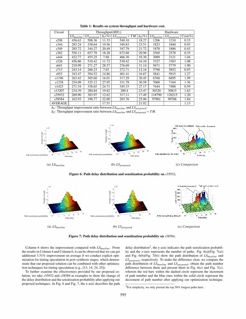
Table 1: Results on system throughput and hardware cost.
Circuit Throughput(MHz) HardwareLSbaseline LSproposed ∆1(%) LSproposed +T M ∆2(%) LSbaseline LSproposed Cost(%)
s298 456.63 508.36 11.33 540.10 18.27 1206 1210 0.33s344 283.24 338.64 19.56 349.83 23.51 1823 1840 0.93s349 285.72 344.27 20.49 347.79 21.72 1878 1886 0.43s382 556.11 657.78 18.28 672.68 20.96 2569 2578 0.35s444 422.77 455.25 7.68 466.30 10.30 3089 3121 1.04s526 456.86 510.42 11.72 530.42 16.10 3327 3363 1.08s641 210.99 271.27 28.57 276.69 31.14 5671 5779 1.90s713 243.14 260.23 7.03 272.71 12.16 5798 5852 0.93s953 343.47 394.52 14.86 401.41 16.87 5841 5915 1.27
s1196 263.42 305.60 16.01 317.29 20.45 6760 6895 1.99s1238 254.09 325.12 27.95 331.78 30.58 7068 7164 1.36s1423 271.54 338.65 24.71 345.33 27.17 7444 7488 0.59s13207 234.39 280.84 19.82 289.4 23.47 30320 30815 1.63s35932 269.90 303.97 12.62 317.11 17.49 118790 120215 1.20s38584 162.93 198.77 22.00 203.76 25.06 97901 99706 1.84
AVERAGE 17.51 21.02 1.13∆1: Throughput improvement ratio between LSbaseline and LSproposed ;∆2: Throughput improvement ratio between LSbaseline and LSproposed +T M.
5 10 15 20 25 30
0
10
20
30
0
0.5
1
1.5
2
x 104
Path delayPath sensitization probability
Nu
mb
er o
f p
ath
(a) LSbaseline
5 10 15 20 25 30
0
10
20
30
0
0.5
1
1.5
2
x 104
Path delayPath sensitization probability
Nu
mb
er o
f p
ath
(b) LSproposed (c) Comparison
Figure 6: Path delay distribution and sensitization probability on s35932.
5 10 15 20 25 30
0
10
20
30
0
0.5
1
1.5
2
x 104
Path delayPath sensitization probability
Nu
mb
er o
f p
ath
(a) LSbaseline
1020
30
0
10
20
30
0
0.5
1
1.5
2
x 104
Path delayPath sensitization probability
Nu
mb
er o
f p
ath
(b) LSproposed (c) Comparison
Figure 7: Path delay distribution and sensitization probability on s38584.
Column 6 shows the improvement compared with LSbaseline. Fromthe results in Column 4 and Column 6, it can be observed that we can getadditional 3.51% improvement on average if we conduct explicit opti-mization for timing speculation in post-synthesis stages, which demon-strate that our proposed solution can be combined with other optimiza-tion techniques for timing speculation (e.g., [13, 14, 24, 25]).
To further examine the effectiveness provided by our proposed so-lution, we take s35932 and s38584 as examples to show the change ofthe delay distribution and the sensitization probability after applying ourproposed techniques. In Fig. 6 and Fig. 7, the x-axis describes the path
delay distribution2, the y-axis indicates the path sensitization probabil-ity and the z-axis represents the number of paths. Fig. 6(a)(Fig. 7(a))and Fig. 6(b)(Fig. 7(b)) show the path distribution of LSbaseline andLSproposed , respectively. To make the difference clear, we compare thepath distribution of LSbaseline and LSproposed , obtain the path numberdifference between them and present them in Fig. 6(c) and Fig. 7(c),wherein the red bars within the dashed circle represent the incrementof path number and the blue ones within the solid circle represent thedecrement of path number after applying our optimization technique.
2For simplicity, we only present the top 50% longest paths here.
595

0
0.05
0.1
0.15
0.2
0.25
0.3
0.55 0.65 0.75 0.85 0.95
Pe
Clock Period
LSproposed
LSbaseline
(a) Timing error probabilities on s35932.
0
0.02
0.04
0.06
0.08
0.1
0.12
0.55 0.65 0.75 0.85 0.95
Pe
Clock PeriodLSbaseline
LSproposed
(b) Timing error probabilities on s38584.
Figure 5: Comparison between LSbaseline and LSproposed .
From these two figures, we can see that the number of the paths withsmaller delay or sensitization probability is increased while the numberof the paths with larger delay or sensitization probability is decreased,which demonstrate why the proposed technique is effective.
Finally, we show the changes of timing error probabilities with re-spect to clock period (set as a percentage of the longest path delay) inFig. 5. Again, from this figure, we can observe that for many of thedifferent clock periods, the timing error probability for LSproposed is re-duced when compared with that of LSbaseline, which is the reason thatthe circuit throughput is improved. This also proves the effectiveness ofthe proposed solution.
5. CONCLUSIONIn this paper, we propose to conduct logic synthesis for timing spec-
ulation from the ground up. Being able to change the logic structure toreduce timing error probability, the proposed solution facilitates to im-prove the throughput and/or energy-efficiency of circuits equipped withtiming speculation capability.
6. ACKNOWLEDGEMENTSThis work was supported in part by the Hong Kong SAR Research
Grants Council under General Research Fund No. CUHK418111.
7. REFERENCES
[1] S. Borkar, et al., “Parameter variations and impact on circuits andmicroarchitecture,” in Proc. ACM/IEEE Design Automation Conference(DAC), 2003, pp. 338–342.
[2] K. Bowman, et al., “Circuit techniques for dynamic variation tolerance,”in Proc. ACM/IEEE Design Automation Conference (DAC), 2009, pp.4–7.
[3] D. Ernst, et al., “Razor: a low-power pipeline based on circuit-leveltiming speculation,” in Proc. IEEE/ACM International Symposium onMicroarchitecture, 2003, pp. 7–18.
[4] B. Greskamp and J. Torrellas, “Paceline: Improving single-threadperformance in nanoscale cmps through core overclocking,” in Proc.International Conference on Parallel Architecture and CompilationTechniques, 2007, pp. 213–224.
[5] L. Benini, E. Macii, M. Poncino, and G. D. Micheli, “Telescopic units: Anew paradigm for performance optimization of vlsi designs,” IEEE Trans.Computer-Aided Design, vol. 17, pp. 220–232, 1998.
[6] D. Frank, R. Puri, and D. Toma, “Design and CAD Challenges in 45nmCMOS and beyond,” in Proc. International Conference onComputer-Aided Design (ICCAD), 2006, pp. 329–333.
[7] S. Borkar, “Designing reliable systems from unreliable components: thechallenges of transistor variability and degradation,” IEEE Micro, vol. 25,no. 6, pp. 10–16, 2005.
[8] C. Metra, M. Favalli, and B. Ricco, “On-line detection of logic errors dueto crosstalk, delay, and transient faults,” in Proc. IEEE International TestConference (ITC), 1998, pp. 524–533.
[9] M. R. Choudhury and K. Mohanram, “TIMBER: Time borrowing anderror relaying for online timing error resilience,” in Proc. Design,Automation, and Test in Europe (DATE), 2010, pp. 1554–1559.
[10] R. Sproull, I. Sutherland, and C. Molnar, “The counterflow pipelineprocessor architecture,” IEEE Design & Test of Computers, vol. 11, no. 3,p. 48, 1994.
[11] L. Wan and D. Chen, “Dynatune: circuit-level optimization for timingspeculation considering dynamic path behavior,” in Proc. InternationalConference on Computer-Aided Design (ICCAD), 2009, pp. 172–179.
[12] B. Greskamp, et al., “Blueshift: Designing processors for timingspeculation from the ground up,” in IEEE International Symposium onHigh Performance Computer Architecture, 2009, pp. 213–224.
[13] A. B. Kahng, S. Kang, R. Kumar, and J. Sartori, “Slack redistribution forgraceful degradation under voltage overscaling,” in Proc. Asia and SouthPacific Design Automation Conference, 2010, pp. 825–831.
[14] Y. Liu, F. Yuan and Q. Xu, “Re-synthesis for cost-efficient circuit-leveltiming speculation,” in Proc. ACM/IEEE Design Automation Conference(DAC), 2011, pp. 158–163.
[15] J. Cong and K. Minkovich, “Logic synthesis for better than worst-casedesigns,” in Proc. International Symposium on VLSI Design, Automationand Test, 2009, pp. 166 –169.
[16] A. Mishchenko, S. Chatterjee, and R. Brayton, “DAG-aware AIGrewriting a fresh look at combinational logic synthesis,” in Proc. DesignAutomation Conference, 2006, pp. 532–535.
[17] ABC: http://www.eecs.berkeley.edu/ alanmi/abc/.[18] J. Cortadella, “Timing-driven logic bi-decomposition,” IEEE Transactions
on Computer-Aided Design of Integrated Circuits and Systems, vol. 22,no. 6, pp. 675 – 685, June 2003.
[19] A. C. Ling, J. Zhu, and S. D. Brown, “Delay driven AIG restructuringusing slack budget management,” in Proc. ACM Great Lakes symposiumon VLSI, 2008, pp. 163–166.
[20] K.C. Chen, et al., “DAG-map: graph-based FPGA technology mappingfor delay optimization,” IEEE Design & Test of Computers, vol. 9, no. 3,pp. 7 –20, Sep. 1992.
[21] K.J. Singh, “Timing optimization of combinational logic,” in Proc.International Conference on Computer-Aided Design (ICCAD), 1988, pp.282–285.
[22] S. Chatterjee, et al., “Reducing structural bias in technology mapping,” inProc. International Conference on Computer-Aided Design (ICCAD),2005, pp. 519–526.
[23] M. Kruijf, S. Nomura, K. Sankaralingam, “A unified model for timingspeculation: Evaluating the impact of technology scaling, CMOS designstyle, and fault recovery mechanism,” in Proc. International Conferenceon Dependable Systems and Networks, 2010 , pp.487-496.
[24] R. Ye, F. Yuan and Q. Xu, “Online clock skew tuning for timingspeculation,” in Proc. IEEE/ACM International Conference onComputer-Aided Design (ICCAD), 2011, pp. 442–447.
[25] R. Ye, F. Yuan, H. Zhou and Q. Xu, “Clock skew scheduling for timingspeculation,” in Proc. IEEE/ACM Design, Automation, and Test in Europe(DATE), 2012, pp. 929–934.
596