
HP 16555A/D 110-MHz State/500-MHz Timing Logic …nagui/labequip/la/16555A D Logic... · ·...
141
Service Guide Publication number 16555-97012 First edition, October 1996 For Safety information, Warranties, and Regulatory information, see the pages at the end of the book. Copyright Hewlett-Packard Company 1987–1996 All Rights Reserved. HP 16555A/D 110-MHz State/ 500-MHz Timing Logic Analyzers
-
Upload
truongduong -
Category
Documents
-
view
213 -
download
1
Transcript of HP 16555A/D 110-MHz State/500-MHz Timing Logic …nagui/labequip/la/16555A D Logic... · ·...

Service Guide
Publication number 16555-97012First edition, October 1996
For Safety information, Warranties, and Regulatoryinformation, see the pages at the end of the book.
Copyright Hewlett-Packard Company 1987–1996
All Rights Reserved.
HP 16555A/D 110-MHz State/ 500-MHz Timing Logic Analyzers

Notice
Hewlett-Packard to Agilent Technologies TransitionThis manual may contain references to HP or Hewlett-Packard. Please note that Hewlett-Packard’s former test and measurement, semiconductor products and chemical analysis businesses are now part of Agilent Technologies. To reduce potential confusion, the only change to product numbers and names has been in the company name prefix: where a product name/number was HP XXXX the current name/number is now Agilent XXXX. For example, model number HP8648 is now model number Agilent 8648.
Contacting Agilent Sales and Service Offices
The sales and service contact information in this manual may be out of date. The latest service and contact information for your location can be found on the Web at:
http://www.agilent.com/find/assist
If you do not have access to the Internet, contact your field engineer or the nearest sales and service office listed below. In any correspondence or telephone conversation, refer to your instrument by its model number and full serial number.
United States(tel) 1 800 452 4844 (fax) 1 800 829 4433
Latin America(tel) (305) 269 7500(fax) (305) 269 7599
New Zealand(tel) 0 800 738 378(fax) 64 4 495 8950
Canada(tel) +1 877 894 4414(fax) +1 888 900 8921
Japan(tel) (81) 426 56 7832(fax) (81) 426 56 7840
Asia Pacific(tel) (852) 3197 7777(fax) (852) 2506 9284
Europe(tel) (31 20) 547 2323(fax) (31 20) 547 2390
Australia(tel) 1 800 629 485(fax) (61 3) 9210 5947
Printed in USA July 2004

HP 16555A/D 110-MHz State/500-MHz Timing Logic Analyzers
The HP 16555A/D are 110-MHz State/500-MHz Timing Logic Analyzer modules forthe HP 16500B/C Logic Analysis Systems. The HP 16555A/D offer high performancemeasurement capability. The HP 16555D has twice the memory depth of the HP 16555A.
Features
Some of the main features of the HP 16555A/D are as follows:
• 64 data channels
• 4 clock/data channels
• 1016K memory depth per channel for the HP 16555A, 2032K memory depth perchannel for the HP 16555D
• 110 MHz maximum state acquisition speed
• 500 MHz maximum timing acquisition speed
• Expandable to 204 channels
Service Strategy
The service strategy for this instrument is the replacement of defective assemblies.This service guide contains information for finding a defective assembly by testingand servicing the HP 16555A/D state and timing analyzer modules.
This module can be returned to Hewlett-Packard for all service work, includingtroubleshooting. Contact your nearest Hewlett-Packard Sales Office for more details.
ii

The HP 16555A/D Logic Analyzer
iii

In This Book
This book is the service guide for the HP 16555A/D 110-MHz State/500-MHz Timing LogicAnalyzer module. Place this service guide in the 3-ring binder supplied with your HP 16500B Logic Analysis System Service Manual or HP 16500C Logic Analysis System
Service Manual.
This service guide is divided into eight chapters.
Chapter 1 contains information about the module and includes accessories for the module,specifications and characteristics of the module, and a list of the equipment required forservicing the module.
Chapter 2 tells how to prepare the module for use.
Chapter 3 gives instructions on how to test the performance of the module.
Chapter 4 contains calibration instructions for the module.
Chapter 5 contains self-tests and flowcharts for troubleshooting the module.
Chapter 6 tells how to replace the module and assemblies of the module and how to returnthem to Hewlett-Packard.
Chapter 7 lists replaceable parts, shows an exploded view, and gives ordering information.
Chapter 8 explains how the analyzer works and what the self-tests are checking.
iv

Contents
1 General Information
Accessories 1-2Operating System 1-2Specifications 1-3Characteristics 1-4Supplemental Characteristics 1-4Recommended Test Equipment 1-7
2 Preparing For Use
To inspect the module 2-2To prepare the mainframe 2-3To configure a one-card module 2-4To configure a multicard module 2-5To install the module 2-10To turn on the system 2-11To test the module 2-11To install the ferrites 2-12
3 Testing Performance
To perform the self-tests and make the test connectors 3-3To test the threshold accuracy 3-9To test the single-clock, single-edge, state acquisition 3-18To test the multiple-clock, multiple-edge, state acquisition 3-30To test the single-clock, multiple-edge, state acquisition 3-41To test the time interval accuracy 3-51To perform the multicard test 3-57Performance Test Record 3-67
4 Calibrating
5 Troubleshooting
To use the flowcharts 5-2To run the self-tests 5-7To run the Board Verification tests 5-8To run the Acquisition IC Verification tests 5-10To test the cables 5-13To test the auxiliary power 5-17
6 Replacing Assemblies
To remove the module 6-2To replace the circuit board 6-3To replace the module 6-3To replace the probe cable 6-5To replace the Reference Clock cable 6-6To return assemblies 6-7
v

7 Replaceable Parts
Replaceable Parts Ordering 7-2Replaceable Parts List 7-3Exploded View 7-5
8 Theory of Operation
Block-Level Theory 8-2Self-Tests Description 8-6
Contents
vi

1
Accessories 1-2Operating System 1-2Specifications 1-3Characteristics 1-4Supplemental Characteristics 1-4Recommended Test Equipment 1-7
General Information

General Information
This chapter lists the accessories, the specifications and characteristics, and therecommended test equipment.
Accessories
The following accessories are supplied with the HP 16555A/D Logic Analyzer.
Accessories Supplied HP Part Number
Probe Tip Assembly, Qty 4 01650-61608
Grabbers, Qty 4 packages 5090-4356
Extra Probe Leads, Qty 1 package 5959-9333
Extra Probe Grounds, Qty 4 packages 5959-9334
Probe Cables, Qty 2 16555-61606
Probe Cable and Pod Labels, Qty 1 01650-94310
Double Probe Adapter, Qty 1 16542-61607
Ferrite Core Assembly, Qty 2 16555-60001
Accessories Available
The accessories available for the HP 16555A/D are listed in the Accessories for HP Logic
Analyzers brochure.
Operating System
With HP 16500B Mainframe
The HP 16555D Logic Analyzer requires operating system version v3.10 or higher.
For the HP 16555A, the version of the operating system software depends on theprogrammable logic device that is the CPU interface. To verify the version of theprogrammable device, first locate the device, which is at the front of the HP 16555A board. Ifthe programmable device has part number 16555-80001, then the device requires operatingsystem version v2.xx, and the maximum state acquisition speed is 100 MHz. If the device haspart number 16555-80002 or higher, then the device requires operating system v3.00 orhigher, and the maximum state acquisition speed is 110 MHz for single-clock, single-edgeclocking mode. You should always use the latest release, and must use version numbers thatare compatible with your device.
With HP 16500C Mainframe
The HP 16555A/D Logic Analyzer requires operating system version v1.00 or higher.
1–2

Specifications
The specifications are the performance standards against which the product is tested.
Minimum State Clock Pulse Width 1 3.5 ns
Threshold Accuracy ± (100 mV + 3% of threshold setting)
Clock Scheme:
Single Clock, Single Edge:
Setup/Hold Time: 1 0.0/3.5 ns through 3.5/0.0 ns, adjustable in 500-ps increments
Maximum State Speed 110 MHz 2
Minimum Master-to-Master Clock Time 1 9.09 ns 2
Single Clock, Multiple Edges:
Setup/Hold Time: 1 0.0/4.0 ns through 4.0/0.0 ns, adjustable in 500-ps increments
Maximum State Speed 100 MHz
Minimum Master-to-Master Clock Time 1 10.0 ns
Multiple Clocks, Multiple Edges:
Setup/Hold Time: 1 0.0/4.5 ns through 4.5/0.0 ns, adjustable in 500-ps increments
Maximum State Speed 100 MHz
Minimum Master-to-Master Clock Time 1 10.0 ns
1 Specified for an input signal VH = −0.9 V, VL = −1.7 V, and threshold = −1.3 V.
2 An HP 16555A in an HP 16500B mainframe using operating system v2.xx has maximum state speed of 100 MHz and minimum Master-to-Master Clock Time of 10.0 ns for single-clock, single-edge clocking. 110-MHz single-clock state acquisition mode is available with HP 16500B mainframe operating system v3.00 or higher or HP 16500C mainframe operating system v1.00 or higher (refer to "Operating System"). The maximum state acquisition speed is 100 MHz for all other clocking modes.
General InformationSpecifications
1–3

Characteristics
The characteristics are not specifications, but are included as additional information.
Full Channel Half Channel *
Maximum State Clock Rate 110 MHz Not applicable
Maximum Conventional Timing Rate 250 MHz 500 MHz
Channel Count per Card 68 34
Channel Count per Three-Card Module 204 102
Memory Depth (HP 16555A) 1016K 2088K
Memory Depth (HP 16555D) 2032K 4177K* Half channel mode is only available for timing analysis.
Supplemental Characteristics
Probes
Input Resistance 100 kΩ, ± 2%
Input Capacitance ~ 8 pF
Minimum Voltage Swing 500 mV, peak-to-peak
Maximum Input Voltage ± 40 V, CAT I
Threshold Range ± 6.0 V, adjustable in 50-mV increments
Clock In/Out
Clock Output 850 mV @100 MHz, terminated into 50 Ω.
Clock Input 1.0 V @100 MHz, ± 20 Vdc offset (clock input portis terminated internally to 50 Ω).
State Analysis
State/Clock Qualifiers 4
Time Tag Resolution* 8 ns
Maximum Time Count Between States 34 seconds
Maximum State Tag Count* 4.29 x 10⁹
Timing Analysis
Sample Period Accuracy 0.01 % of sample period
Channel-to-Channel Skew 2 ns, typical
Time Interval Accuracy ± [sample period + channel-to-channel skew +(0.01%)(time reading)]
General InformationCharacteristics
1–4

Triggering
Sequencer Speed 125 MHz, maximum
State Sequence Levels 12
Timing Sequence Levels 10
Maximum Occurrence Counter Value 1,048,575
Pattern Recognizers 10
Maximum Pattern Width 68 channels in a one-card configuration. 204 channels in a three-card configuration.
Range Recognizers 2
Range Width 32 bits each
Timers 2
Timer Value Range 400 ns to 500 seconds
Glitch/Edge Recognizers 2 (timing only)
Maximum Glitch/Edge Width 68 channels in a one-card configuration.204 channels in a three-card configuration.
*Maximum state clock rate with time or state tags on is 110 MHz. When all pods are assigned to a state or timing machine, time or state tags halve the memory depth.
Measurement and Display Functions
Arming Each module can be armed by the RUN key, by the external PORT IN, or byanother module via the Intermodule Bus (IMB).
Displayed Waveforms 24 lines maximum, with scrolling across 96 waveforms.
Measurement Functions
Run/Stop Functions Run Starts acquisition of data in specified trace mode.
Stop In single trace mode or the first run of a repetitive acquisition, STOP haltsacquisition and displays the current acquisition data. For subsequent runs in repetitivemode, STOP halts acquisition of data and does not change the current display.
Trace Mode Single mode acquires data once per trace specification. Repetitive moderepeats single mode acquisitions until stop is pressed or until the time interval betweentwo specified patterns is less than or greater than a specified value, or within or not withina specified range.
Indicators
Activity Indicators Provided in the Configuration and Format menus for identifyinghigh, low, or changing states on the inputs.
Markers Two markers (X and 0) are shown as dashed lines on the display.
Trigger Displayed as a vertical dashed line in the Timing Waveform display and as line 0in the State Listing display.
General InformationSupplemental Characteristics
1–5

Data Entry/Display
Labels Channels may be grouped together and given a 6-character name. Up to126 labels in each analyzer may be assigned with up to 32 channels per label.
Display Modes State listing, State Waveforms, Chart, Compare Listing, CompareDifference Listing, Timing Waveforms, and Timing Listings. State Listing, TimingWaveforms and Oscilloscope Waveforms can be time-correlated on the same displays.
Timing Waveform Pattern readout of timing waveforms at X or 0 marker.
Bases Binary, Octal, Decimal, Hexadecimal, ASCII (display only), Two’s Complement,and User-defined symbols.
Symbols 1,000 maximum. Symbols can be downloaded over RS-232 or HP-IB.
Marker Functions
Time Interval The X and 0 markers measure the time interval between one point on atiming waveform and trigger, two points on the same timing waveform, two points ondifferent waveforms, or two states (time tagging on).
Delta States (state analyzer only) The X and 0 markers measure the number oftagged states between one state and trigger or between two states.
Patterns The X and 0 markers can be used to locate the nth occurrence of a specifiedpattern from trigger, or from the beginning of data. The 0 marker can also find the nth
occurrence of a pattern from the X marker.
Statistics X and 0 marker statistics are calculated for repetitive acquisitions. Patternsmust be specified for both markers and statistics are kept only when both patterns can befound in an acquisition. Statistics are minimum X to 0 time, maximum X to 0 time,average X to 0 time, and ratio of valid runs to total runs.
Auxiliary Power
Power Through Cables 1/3 amp at 5 V maximum per cable
Operating Environment
Temperature Instrument, 0 °C to 55 °C (+32 °F to 131 °F).Probe lead sets and cables, 0 °C to 65 °C (+32 °F to 149 °F).
Humidity Instrument, probe lead sets, and cables, up to 95% relative humidity at +40 °C (+122 °F).
Altitude To 4600 m (15,000 ft).
Vibration Operating: Random vibration 5 to 500 Hz, 10 minutes per axis, ≈ 0.3 g (rms).
Non-operating: Random vibration 5 to 500 Hz,10 minutes per axis, ≈ 2.41 g (rms); and swept sine resonant search, 5 to 500 Hz,0.75 g (0-peak), 5 minute resonant dwell at 4 resonances per axis.
General InformationSupplemental Characteristics
1–6

Recommended Test Equipment
Equipment Required
Equipment Critical Specifications RecommendedModel/Part
Use*
Pulse Generator 110 MHz, 3.5 ns pulse width, < 600 ps rise time
HP 8131A Option 020 P,T
Digitizing Oscilloscope ≥ 6 GHz bandwidth, < 58 ps rise time HP 54750A mainframewith HP 54751A pluginmodule
P
Function Generator Accuracy ≤(5)(10−6) × frequency,DC offset voltage ±6.3 V
HP 3325B Option 002 P
Digital Multimeter 0.1 mV resolution, 0.005% accuracy HP 3458A PBNC-Banana Cable HP 11001-60001 PBNC Tee BNC (m)(f)(f) HP 1250-0781 PCable BNC (m-m) 48 inch HP 10503A PSMA Coax Cable (Qty 3) ≥ 18 GHz bandwidth HP 8120-4948 PBNC Coax Cable BNC (m-m), >2 GHz bandwidth HP 8120-1840 PAdapter (Qty 4) SMA(m)-BNC(f) HP 1250-1200 PAdapter SMA(f)-BNC(m) HP 1250-2015 PCoupler BNC (m-m) HP 1250-0216 P20:1 Probes (Qty 2) HP 54006A PBNC Test Connector, 17x2(Qty 1)**
P
BNC Test Connector, 6x2(Qty 4)**
P,T
*A = Adjustment P = Performance Tests T = Troubleshooting
**Instructions for making these test connectors are in chapter 3, "Testing Performance."
General InformationRecommended Test Equipment
1–7

1–8

2
To inspect the module 2-2To prepare the mainframe 2-3To configure a one-card module 2-4To configure a multicard module 2-5To install the module 2-10To turn on the system 2-11To test the module 2-11To install the ferrites 2-12
Preparing for Use

Preparing For Use
This chapter gives you instructions for preparing the logic analyzer module for use.
Power Requirements
All power supplies required for operating the logic analyzer are supplied through thebackplane connector in the mainframe.
Operating Environment
The operating environment is listed in chapter 1. Note the non-condensing humiditylimitation. Condensation within the instrument can cause poor operation ormalfunction. Provide protection against internal condensation.
The logic analyzer module will operate at all specifications within the temperatureand humidity range given in chapter 1. However, reliability is enhanced whenoperating the module within the following ranges:
• Temperature: +20 °C to +35 °C (+68 °F to +95 °F)
• Humidity: 20% to 80% non-condensing
Storage
Store or ship the logic analyzer in environments within the following limits:
• Temperature: -40 °C to +75 °C
• Humidity: Up to 90% at 65 °C
• Altitude: Up to 15,300 meters (50,000 feet)
Protect the module from temperature extremes which cause condensation on theinstrument.
To inspect the module
1 Inspect the shipping container for damage.If the shipping container or cushioning material is damaged, keep them until you havechecked the contents of the shipment and checked the instrument mechanically andelectrically.
2 Check the supplied accessories.Accessories supplied with the module are listed in chapter 1, "Accessories Supplied."
3 Inspect the product for physical damage.Check the module and the supplied accessories for obvious physical or mechanical defects. Ifyou find any defects, contact your nearest Hewlett-Packard Sales Office. Arrangements forrepair or replacement are made, at Hewlett-Packard’s option, without waiting for a claimsettlement.
2–2

To prepare the mainframe
C A U T I O N Turn off the mainframe power before removing, replacing, or installing the module.
C A U T I O N Electrostatic discharge can damage electronic components. Use grounded wriststraps andmats when performing any service to this module.
1 Turn off the mainframe power switch, then unplug the power cord. Disconnect anyinput or output connections.
2 Plan your module configuration.If you are installing a one-card module, use any available slot in the mainframe.
If you are installing a multicard module, use adjacent slots in the mainframe.
3 Loosen the thumb screws.Cards or filler panels below the slots intended for installation do not have to be removed.
Starting from the top, loosen the thumb screws on filler panels and cards that need to bemoved.
4 Starting from the top, pull the cards and filler panels that need to be moved halfwayout.
C A U T I O N All multicard modules will be cabled together. Pull these cards out together.
5 Remove the cards and filler panels.Remove the cards or filler panels that are in the slots intended for the module installation.Push all other cards into the card cage, but not completely in. This is to get them out of theway for installing the module.
Some modules for the Logic Analysis System require calibration if you move them to adifferent slot. For calibration information, refer to the manuals for the individual modules.
Preparing for UseTo prepare the mainframe
2–3

To configure a one-card module
• When shipped separately, the module is configured as a one-card module. Thecables should be connected as shown in the figure.
• To configure a multicard module into one-card modules, remove the cablesconnecting the cards. Then connect the free end of the 2x10 cable to theconnector labeled "Master" (J6) on each card (see figure below).
C A U T I O N If you pull on the flexible ribbon part of the 2x10 cable, you might damage the cableassembly. Using your thumb and finger, grasp the ends of the cable connector. Applypressure to the ends of the cable connector to disengage the metal locking tabs of theconnector from the cable socket on the board. Then pull the connector from the cablesocket.
Save unused cables for future configurations.
Preparing for UseTo configure a one-card module
2–4

To configure a multicard module
1 Plan the configuration. Multicard modules can only be connected as shown in theillustration. Select the card that will be the master card, and set the remaining cardsaside.
Do not combine HP 16555A cards and HP 16555D cards together in a multicard module. Amulticard module with both HP 16555A and HP 16555D cards will not operate.
2 Obtain two 2x25 cables from the accessory pouch that match the number ofexpanders being configured. The illustration shows the cables that are available andwhich cable is used in each expander configuration.
Preparing for UseTo configure a multicard module
2–5

3 Look at the illustration in the previous step. The illustration shows which of thecable connectors is plugged into the master card. Plug one 2x25 cable into themaster card J9. Observe which cable connector (as shown in the illustration) isplugged into J9. Follow the same procedure to connect the second 2x25 cable intothe master card J10.
4 On the expander cards, disconnect the end of the 2x10 cable that is plugged into theconnector labeled "Master."
C A U T I O N If you pull on the flexible ribbon part of the 2x10 cable, you might damage the cableassembly. Using your thumb and finger, grasp the ends of the cable connector. Applypressure to the ends of the cable connector to disengage the metal locking tabs of theconnector from the cable socket on the board. Then pull the connector from the cablesocket.
Preparing for UseTo configure a multicard module
2–6
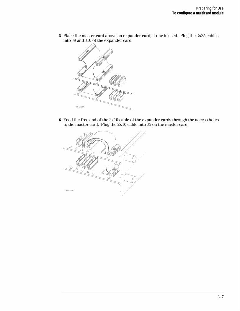
5 Place the master card above an expander card, if one is used. Plug the 2x25 cablesinto J9 and J10 of the expander card.
6 Feed the free end of the 2x10 cable of the expander cards through the access holesto the master card. Plug the 2x10 cable into J5 on the master card.
Preparing for UseTo configure a multicard module
2–7

7 Place the remaining expander board on top of the master board. Feed the 2x25cables that are plugged into the master card through the cable access holes of theexpander card. Plug the 2x25 cables into J9 and J10 of the expander card.
8 Feed the free end of the 2x10 cables of the expander cards through the access holesto the master card. Plug the 2x10 cable into J7 on the master card.
Preparing for UseTo configure a multicard module
2–8

9 The following illustration shows the proper connection of the 2x25 cables and the2x10 cables for a three card module. A two card module is configured in the samemanner, with the expansion card above the master card. Make sure ALL cables arefirmly seated.
Preparing for UseTo configure a multicard module
2–9

To install the module
1 Slide the cards above the slots for the module about halfway out of the mainframe.2 With the probe cables facing away from the instrument, slide the module
approximately halfway into the mainframe.
3 Slide the complete module into the mainframe, but not completely in.Each card in the instrument is firmly seated and tightened one at a time in step 5.
4 Position all cards and filler panels so that the endplates overlap.5 Seat the cards and tighten the thumbscrews.
Starting with the bottom card, firmly seat the cards into the backplane connector of themainframe. Keep applying pressure to the center of the card endplate while tightening thethumbscrews finger-tight. Repeat this for all cards and filler panels starting at the bottom andmoving to the top.
C A U T I O N Correct air circulation keeps the instrument from overheating. For correct air circulation,filler panels must be installed in all unused card slots. Keep any extra filler panels for futureuse.
Preparing for UseTo install the module
2–10

To turn on the system
1 Connect the power cable to the mainframe.2 Turn on the instrument power switch.
When you turn on the instrument power switch, the instrument performs powerup tests thatcheck mainframe circuitry. After the powerup tests are complete, the screen will look similarto the sample screen below.
The screen above is from an HP 16555A Logic Analyzer. The HP 16555D will appear as "2.0M SAMPLE 110/500MHz LA."
To test the module
The logic analyzer module does not require an operational accuracy calibration or adjustment.After installing the module, you can test and use the module.
• If you require a test to verify the specifications, start at the beginning of chapter 3,"Testing Performance."
• If you require a test to initially accept the operation, perform the self-tests inchapter 3.
• If the module does not operate correctly, go to the beginning of chapter 5,"Troubleshooting."
Preparing for UseTo turn on the system
2–11

To install the ferrites
Ferrites are included in the HP 16555A/D accessory pouch for each logic analyzer cable (twopods). When properly installed, the ferrites reduce RFI emissions from the logic analyzermodule.
In order to ensure compliance of the HP 16555A/D analyzer module to the CISPR 11 Class Aradio frequency interference (RFI) limits, you must install the ferrite to absorb radiofrequency energy. Adding or removing the ferrite will not affect the normal operation of theanalyzer.
1 Place the ferrite halves on the logic analyzer cable like a clamshell around the wholecable. The ferrite should be no more than 15 cm (about 6 in) from the rear panel ofthe logic analyzer.
2 Insert the clamps onto the ends of the ferrites. The locking tab should fit cleanly inthe ferrite grooves. When properly installed, the ferrite should appear on the logicanalyzer cable as shown below on the right.
Preparing for UseTo install the ferrites
2–12

3
To perform the self-tests and make the test connectors 3-3To test the threshold accuracy 3-9To test the single-clock, single-edge, state acquisition 3-18To test the multiple-clock, multiple-edge, state acquisition 3-30To test the single-clock, multiple-edge, state acquisition 3-41To test the time interval accuracy 3-51To perform the multicard test 3-57Performance Test Record 3-67
Testing Performance

Testing Performance
This chapter tells you how to test the performance of the logic analyzer against thespecifications listed in chapter 1. To ensure the logic analyzer is operating asspecified, software tests (self-tests) and manual performance tests are done on themodules. The logic analyzer is considered performance-verified if all of the softwaretests and manual performance tests have passed. The procedures in this chapterindicate what constitutes a "Pass" status for each of the tests.
Test Strategy
For a complete test, start at the beginning with the software tests and continuethrough to the end of the chapter. For an individual test, follow the procedure in thetest.
One-card module
To perform a complete test on a one-card module, start at the beginning of thechapter and follow each procedure.
Multicard module
To perform a complete test on a multicard module, perform the software tests withthe cards connected. Then, remove the multicard module from the mainframe andconfigure each card as a one-card module. Install the one-card modules into themainframe and perform the one-card manual performance tests on each card. Whenthe tests are complete, remove the one-card modules, reconfigure them into amulticard module, reinstall the module into the mainframe, then perform the finalmulti-card test. For removal instructions, see chapter 6, "Replacing Assemblies." Forinstallation and configuration instructions, see chapter 2, "Preparing for Use."
Test Interval
Test the performance of the module against specifications at two-year intervals.
Test Record Description
A performance test record for recording the results of each procedure is located atthe end of this chapter. Use the performance test record to gauge the performanceof the module over time.
Test Equipment
Each procedure lists the recommended test equipment. You can use equipment thatsatisfies the specifications given. However, the procedures are based on using therecommended model or part number.
Instrument Warm-Up
Before testing the performance of the module, warm-up the instrument and the testequipment for 30 minutes.
3–2

To perform the self-tests and make the test connectors
The self-tests verify the correct operation of the logic analyzer module. Self-tests canbe performed all at once or one at a time. While testing the performance of themodule, run the self-test all at once.
The test connectors connect the analyzer to the test equipment.
Perform the self-tests
1 Disconnect all inputs. 2 In the System Configuration menu, touch Configuration. In the pop-up, touch Test.
3 Touch the box labeled Touch Box to Load Test System.4 On the test system screen, touch Test System. Select the module to be tested. For
an HP 16555A, select 1M Sample LA as the module to be tested. For an HP 16555D,select 2M Sample LA.
3–3

5 In the Performance Verification menu, touch the field labeled Board Verification.
6 In the Board Verification menu, touch All Tests.You can run all tests at one time by touching All Tests. To see more details about each testwhen troubleshooting failures, you can run each test individually. This example shows how torun all tests at once.
7 When the tests finish, the status will show Passed or Failed. Record the results ofthe Board Verification tests in the performance test record at the end of this chapter.
Testing PerformanceTo perform the self-tests and make the test connectors
3–4

8 Touch Exit to leave the Board Verification menu. In the Performance Verificationmenu, touch the field labeled Acquisition IC Verification.
9 In the Acquisition IC Verification menu, touch All Tests.You can run all tests at one time by touching All Tests. To see more details about each testwhen troubleshooting failures, you can run each test individually. This example shows how torun all tests at once.
10 When the tests finish, the status will show Passed or Failed. Record the results ofthe Acquisition IC Verification tests in the performance test record at the end of thischapter.
Testing PerformanceTo perform the self-tests and make the test connectors
3–5

11 Touch 1M Sample LA (HP 16555A) or 2M Sample LA (HP 16555D). If more logicanalyzer cards are to be tested, select the next card, then repeat the test. When allcards are tested, touch 1M Sample LA (or 2M Sample LA), then select Test System.
12 Touch Configuration, then select Test. In the Test menu, touch the box labeledTouch box to Exit Test System.
Testing PerformanceTo perform the self-tests and make the test connectors
3–6

Make the test connectors
Materials Required
Description Recommended Part Qty
BNC (f) Connector HP 1250-1032 5
100 Ω 1% resistor HP 0698-7212 8
Berg Strip, 17-by-2 1
Berg Strip, 6-by-2 4
20:1 Probe HP 54006A 2
Jumper wire
1 Build four test connectors using BNC connectors and 6-by-2 sections of Berg strip.a Solder a jumper wire to all pins on one side of the Berg strip.
b Solder a jumper wire to all pins on the other side of the Berg strip.
c Solder two resistors to the Berg strip, one at each end between the end pins.
d Solder the center of the BNC connector to the center pin of one row on the Berg strip.
e Solder the ground tab of the BNC connector to the center pin of the other row on theBerg strip.
f On two of the test connectors, solder a 20:1 probe. The probe ground goes to thesame row of pins on the test connector as the BNC ground tab.
Testing PerformanceTo perform the self-tests and make the test connectors
3–7

2 Build one test connector using a BNC connector and a 17-by-2 section of Berg strip.a Solder a jumper wire to all pins on one side of the Berg strip.
b Solder a jumper wire to all pins on the other side of the Berg strip.
c Solder the center of the BNC connector to the center pin of one row on the Berg strip.
d Solder the ground tab of the BNC connector to the center pin of the other row on theBerg strip.
Testing PerformanceTo perform the self-tests and make the test connectors
3–8

To test the threshold accuracy
Testing the threshold accuracy verifies the performance of the following specification:
• Clock and data channel threshold accuracy.
Multicard modules must be reconfigured as one-card modules for this test.
These instructions include detailed steps for testing the threshold settings of pod 1.After testing pod 1, connect and test the rest of the pods one at a time. To test thenext pod, follow the detailed steps for pod 1, substituting the next pod for pod 1 inthe instructions.
Equipment Required
Equipment Critical Specifications Recommended Model/PartDigital Multimeter 0.1 mV resolution, 0.005% accuracy HP 3458AFunction Generator DC offset voltage ±6.3 V HP 3325B Option 002BNC-Banana Cable HP 11001-60001BNC Tee HP 1250-0781BNC Cable HP 8120-1840BNC Test Connector,17x2
Set up the equipment
1 Turn on the equipment required and the logic analyzer. Let them warm up for30 minutes before beginning the test.
2 Set up the function generator.a Set up the function generator to provide a DC offset voltage at the Main Signal output.
b Disable any AC voltage to the function generator output, and enable the high voltageoutput.
c Monitor the function generator DC output voltage with the multimeter.
3–9

Set up the logic analyzer
1 In the System Configuration menu, touch System, then select 1M Sample LA (HP 16555A) or 2M Sample LA (HP 16555D).
2 In the Configuration menu, unassign Pod 3 and Pod 4. To unassign the pods, touchthe Pod 3, Pod 4 field, then select Unassigned.
Connect the logic analyzer
1 Using the 17-by-2 test connector, BNC cable, and probe tip assembly, connect thedata and clock channels of Pod 1 to one side of the BNC Tee.
2 Using a BNC-banana cable, connect the voltmeter to the other side of the BNC Tee.3 Connect the BNC Tee to the Main Signal output of the function generator.
Pod 3, Pod 4 field
Testing PerformanceTo test the threshold accuracy
3–10

Test the TTL threshold
1 In the Configuration menu, touch Configuration, then touch Format. In the Formatmenu, touch the field to the right of Pod 1, then select TTL.
2 On the function generator front panel, enter 1.647 V ±1 mV DC offset. Use themultimeter to verify the voltage.The activity indicators for Pod 1 should show all data channels and the J-clock channel at alogic high.
3 Using the Modify down arrow on the function generator, decrease offset voltage in1-mV increments until all activity indicators for Pod 1 show the channels at a logiclow. Record the function generator voltage in the performance test record.
Testing PerformanceTo test the threshold accuracy
3–11

4 Using the Modify up arrow on the function generator, increase offset voltage in1-mV increments until all activity indicators for Pod 1 show the channels at a logichigh. Record the function generator voltage in the performance test record.
Testing PerformanceTo test the threshold accuracy
3–12

Test the ECL threshold
1 In the Format menu, touch the field to the right of Pod 1, then select ECL.2 On the function generator front panel, enter −1.159 V ±1 mV DC offset. Use the
multimeter to verify the voltage.The activity indicators for Pod 1 should show all data channels and the J-clock channel at alogic high.
3 Using the Modify down arrow on the function generator, decrease offset voltage in1-mV increments until all activity indicators for Pod 1 show the channels are at alogic low. Record the function generator voltage in the performance test record.
4 Using the Modify up arrow on the function generator, increase offset voltage in1-mV increments until all activity indicators for Pod 1 show the channels are at alogic high. Record the function generator voltage in the performance test record.
Testing PerformanceTo test the threshold accuracy
3–13

Test the − User threshold
1 In the Format menu, touch the field to the right of Pod 1, then select User. In thepop-up menu, enter −6.00 V, then touch Done.
2 On the function generator front panel, enter −5.718 V ±1 mV DC offset. Use themultimeter to verify the voltage.The activity indicators for Pod 1 should show all data channels and the J-clock channel at alogic high.
3 Using the Modify down arrow on the function generator, decrease offset voltage in1-mV increments until all activity indicators for Pod 1 show the channels at a logiclow. Record the function generator voltage in the performance test record.
4 Using the Modify up arrow on the function generator, increase offset voltage in1-mV increments until all activity indicators show the channels at a logic high.Record the function generator voltage in the performance test record.
Testing PerformanceTo test the threshold accuracy
3–14

Test the + User threshold
1 In the Format menu, touch the field to the right of Pod 1, then select User. In thepop-up menu, enter +6.00 V, then touch Done.
2 On the function generator front panel, enter +6.282 V ±1 mV DC offset. Use themultimeter to verify the voltage.The activity indicators for Pod 1 should show all data channels and the J-clock channel at alogic high.
3 Using the Modify down arrow on the function generator, decrease offset voltage in1-mV increments until all activity indicators for Pod 1 show the channels at a logiclow. Record the function generator voltage in the performance test record.
4 Using the Modify up arrow on the function generator, increase offset voltage in1-mV increments until all activity indicators for Pod 1 show the channels at a logichigh. Record the function generator voltage in the performance test record.
Testing PerformanceTo test the threshold accuracy
3–15

Test the 0 V User threshold
1 In the Format menu, touch the field to the right of Pod 1, then select User. In thepop-up menu, enter 0.00 V, then touch Done.
2 On the function generator front panel, enter +0.102 V ±1 mV DC offset. Use themultimeter to verify the voltage.The activity indicators for Pod 1 should show all data channels and the J-clock channel at alogic high.
3 Using the Modify down arrow on the function generator, decrease offset voltage in1-mV increments until all activity indicators for Pod 1 show the channels at a logiclow. Record the function generator voltage in the performance test record.
4 Using the Modify up arrow on the function generator, increase offset voltage in1-mV increments until all activity indicators for Pod 1 show the channels at a logichigh. Record the function generator voltage in the performance test record.
Testing PerformanceTo test the threshold accuracy
3–16

Test the next pod
Using the 17-by-2 test connector and probe tip assembly, connect the data and clock channelsof the next pod to the output of the function generator.
• If you just finished testing Pod 1, connect the data and clock channels of Pod 2.Start with "Test the TTL threshold" on page 3–11, substituting Pod 2 for Pod 1.
• If you just finished testing Pod 2, connect the data and clock channels of pod 3. Inthe logic analyzer Configuration menu, unassign Pods 1 and 2, assign Pods 3 and 4 toMachine 1. Start with "Test the TTL threshold" on page 3–11, substituting Pod 3 forPod 1.
• If you just finished testing Pod 3, connect the data and clock channels of Pod 4.Start with "Test the TTL threshold" on page 3–11, substituting Pod 4 for Pod 1.
• If you just finished testing Pod 4, you have completed the threshold accuracy test.
Testing PerformanceTo test the threshold accuracy
3–17

To test the single-clock, single-edge, state acquisition
Testing the single-clock, single-edge, state acquisition verifies the performance of thefollowing specifications:
• Minimum master to master clock time.
• Maximum state acquisition speed.
• Setup/Hold time.
• Minimum clock pulse width.
Multicard modules must be reconfigured as one-card modules for this test.
This test checks a combination of data channels using a single-edge clock at threeselected setup/hold times.
Equipment Required
Equipment Critical Specifications RecommendedModel/Part
Pulse Generator 110 MHz 3.5 ns pulse width, <600 ps rise time HP 8131A option 020Digitizing Oscilloscope ≥ 6 GHz bandwidth, <58 ps rise time HP 54750A w/ HP 54751AAdapter SMA(m)-BNC(f) HP 1250-1200SMA Coax Cable (Qty 3) HP 8120-4948Coupler (Qty 3) BNC(m-m) HP 1250-0216BNC Test Connector, 6x2 (Qty 3)
Set up the equipment
1 Turn on the equipment required and the logic analyzer. Let them warm up for30 minutes before beginning the test if you have not already done so.
2 Set up the pulse generator according to the following table.
Pulse Generator Setup
Channel 1 Channel 2 Period
Delay: 0 ps Doub: 9.05 ns * 18.1 ns *
Width: 3.5 ns Width: 3.5 ns
High: -0.9 V High: -0.9 V
Low: -1.7 V Low: -1.7 V
COMP: Disabled(LED off)
COMP: Disabled(LED off)
* If running HP 16500B mainframe software version v2.xx on an HP 16555A, set Channel 2 Doub: 10 ns, and Period to 20 ns. 110-MHz single-clock state acquisition mode is available with HP 16500B mainframe operating system v3.00 or higher or HP 16500C mainframe operating system v1.00 or higher. For information on software version, refer to "Operating System" in chapter 1.
3–18

3 Set up the oscilloscope.a Select Setup, then select Default Setup.
b Configure the oscilloscope according to the following table.
Oscilloscope Setup
Acquisition Display Trigger [Shift] ∆ Time
Averaging: On# of averages: 16
Graticule Graphs: 2
Level: -250 mV Stop src: channel 2 [Enter]
Channel 1 Channel 2 Define meas
Alternate Scale Attenuation: 20.00:1Scale: 200 mV/divOffset: −1.300 V
Alternate Scale Attenuation: 20.00:1Scale: 200 mV/divOffset: -1.300 V
Thresholds: user-defined Units: Volts Upper: -980 mV Middle: -1.30 V Lower: -1.62 V
Set up the logic analyzer
1 Set up the Configuration menu.a In the System Configuration menu, touch System, then select 1M Sample LA (2M
Sample LA for HP 16555D).
b In the Configuration menu, assign all pods to Machine 1. To assign the pods, touch thepod fields, then select Machine 1.
c In the Analyzer 1 box, touch the Type field, then select State.
Testing PerformanceTo test the single-clock, single-edge, state acquisition
3–19

2 Set up the Format menu.a Touch Configuration, then select Format.
b Touch the field to the right of each Pod field, then select ECL. The screen does notshow all Pod fields at one time. To access more Pod fields, turn the knob.
c Touch the field showing the channel assignments for one of the pods being tested. Inthe pop-up menu, touch Clear until all "." appear. Using the knob, move the cursor tothe data channels to be tested (channel 11 and channel 3 of each pod). Touch theasterisk field to put asterisks in the channel positions, activating the channels, thentouch Done. Follow this step for the remaining three pods.
d Touch the State Acquisition Mode field, then select 110MHz/1M State (110MHz/2MState for HP 16555D).*
*110-MHz single-clock state acquisition mode is not available with HP 16555A operating system v2.xx . Refer to page 1-2
3 Set up the Trigger menu.a Touch Format, then select Trigger. In the Trigger menu, touch Modify Trigger, then
select Clear Trigger, then select All.
b Touch the Count Off field. In the Count menu, touch Off. In the pop-up, select Time,then touch Done to exit.
c Touch the Acquisition Control field. In the Acquisition Control menu, touch TriggerPosition then touch Start. Touch Memory Length, and at the numeric keypad, enter"4096" and Touch Done. Touch Done to exit the menu.
d Touch the field labeled "1" under the State Sequence Levels. Touch the field labeled"anystate," then select "no state." Touch Done.
e Touch the pattern recognizer "a." In the pop-up menu, type "AA," then touch Done.
Testing PerformanceTo test the single-clock, single-edge, state acquisition
3–20

4 Set up the Listing menu.a Touch Trigger, then select Listing.
b Touch the Markers field, then select Pattern.
c Touch Specify Patterns. Select the X Marker > field. At the numeric keypad, enter"AA." Select the O Marker > field. At the numeric keypad, enter "55." Touch Done.
d Touch the Find X-pattern occurrences field. At the numeric keypad, enter "2047."Touch Done.
e Touch the Find X-pattern field. The field should toggle to Find O-pattern.
f Touch the Find O-pattern occurrences field. At the numeric keypad, enter "2048."Touch Done.
Testing PerformanceTo test the single-clock, single-edge, state acquisition
3–21

Connect the logic analyzer
1 Using the 6-by-2 test connectors, connect the logic analyzer clock and data channelslisted in the table below to the pulse generator.
2 Using SMA cables, connect channel 1, channel 2, and trigger from the oscilloscopeto the pulse generator.
Connect the Logic Analyzer to the Pulse Generator
Connect to HP 8131A Channel 1 Output
Connect to HP 8131AChannel 1 Output
Connect to HP 8131AChannel 2 Output
Pod 1, channel 3Pod 2, channel 3Pod 3, channel 3Pod 4, channel 3
Pod 1, channel 11Pod 2, channel 11Pod 3, channel 11Pod 4, channel 11
J-clockK-clockL-clockM-clock
Testing PerformanceTo test the single-clock, single-edge, state acquisition
3–22

Verify the test signal
1 Check the clock pulse width. Using the oscilloscope, verify that the clock pulsewidth is 3.480 ns, +20 ps or -80 ps. a Enable the pulse generator channel 1 and channel 2 outputs (LED off).
b In the oscilloscope Timebase menu, select Scale: 1.000 ns/div.
c In the oscilloscope Timebase menu, select Position. Using the oscilloscope knob,position the clock waveform so that the waveform is centered on the screen.
d On the oscilloscope, select [Shift] + width: channel 2, then select [Enter] to display theclock signal pulse width (+ width(2)).
e If the pulse width is outside the limits, adjust the pulse generator channel 2 width untilthe pulse width is within limits.
Testing PerformanceTo test the single-clock, single-edge, state acquisition
3–23

2 Check the clock period. Using the oscilloscope, verify that the master-to-masterclock time is 9.05 ns. * a In the oscilloscope Timebase menu, select Scale: 2.000 ns/div.
b In the oscilloscope Timebase menu, select Position. Using the oscilloscope knob,position the clock waveform so that a rising edge appears at the left of the display.
c On the oscilloscope, select [Shift] Period: channel 2, then select [Enter] to display theclock period (Period(2)). If the period is not less than 9.05 ns, go to step d. If theperiod is less than 9.05 ns, go to step 3.
d In the oscilloscope Timebase menu, increase Position 9.000 ns. If the period is not lessthan 9.05 ns, decrease the pulse generator Chan 2 Doub in 10 ps increments until oneof the two periods measured is less than 9.05 ns.
*If running operating system version HP 16555A operating system v2.xx, measure a master-to-master clock time of 10 ns.
3 Check the data pulse width. Using the oscilloscope, verify that the data pulse widthis 3.480 ns, +20 ps or - 80 ps. a In the oscilloscope Timebase menu, select Scale: 1.000 ns/div.
b In the oscilloscope Timebase menu, select Position. Using the oscilloscope knob,position the data waveform so that the waveform is centered on the screen.
c On the oscilloscope, select [Shift] + width: channel 1, then select [Enter] to display thedata signal pulse width (+ width(1)).
d If the pulse width is outside the limits, adjust the pulse generator channel 1 width untilthe pulse width is within limits.
Testing PerformanceTo test the single-clock, single-edge, state acquisition
3–24

Check the setup/hold combination
1 Select the logic analyzer setup/hold time.a Touch Listing, then touch Format.
b In the logic analyzer Format menu, touch Master Clock.
c Touch the Setup/Hold field and select the setup/hold combination to be tested for allpods. The first time through this test, select the top combination in the following table.
Setup/Hold Combinations
3.5/0.0 ns
0.0/3.5 ns
1.5/2.0 ns
d Touch Done to exit the setup/hold combinations.
2 Disable the pulse generator channel 2 COMP (LED off).
Testing PerformanceTo test the single-clock, single-edge, state acquisition
3–25

3 Using the Delay mode of the pulse generator channel 1, position the pulsesaccording to the setup/hold combination selected, +0.0 ps or -100 ps. a On the Oscilloscope, select [Define meas] Define ∆Time - Stop edge: rising.
b In the oscilloscope timebase menu, select Position. Using the oscilloscope knob,position the rising edge of the clock waveform so that it is centered on the display.
c On the oscilloscope, select [Shift] ∆ Time, then select [Enter] to display the setup time(∆Time(1)-(2)).
d Adjust the pulse generator channel 1 Delay until the pulses are aligned according thethe setup time of the setup/hold combination selected, +0.0 ps or -100 ps.
4 Select the clock to be tested.a In the Master Clock menu, touch the clock field to be tested and then select the clock
edge as indicated in the table. The first time through this test, select the first clockand edge.
Clocks
J↑ K↑ L↑ M↑
b Touch Done to exit the Master Clock menu.
Note: The Master Clock menu shown is for an HP 16555A 1M Sample analyzer running in 110-MHz mode. If HP 16555A operating system version v2.xx is being used, the Master Clock menu will look similar to that shown on page 3-38.
Testing PerformanceTo test the single-clock, single-edge, state acquisition
3–26

5 In the logic analyzer Format menu, touch Run. The display should show analternating pattern of "AA" and "55." If the "Search Failed" yellow bar message doesnot appear, the test passes. Record the Pass or Fail in the performance test record.
6 Test the next clock.a Touch Listing, then touch Format.
b In the logic analyzer Format menu, touch Master Clock.
c Turn off the clock just tested.
d Repeat steps 4, 5, and 6 for the next clock edge listed in the table in step 4, until alllisted clock edges have been tested.
7 Enable the pulse generator channel 2 COMP (LED on).8 Using the Delay mode of the pulse generator channel 1, position the pulses
according to the setup/hold combination selected, +0.0 ps or -100 ps. a On the Oscilloscope, select [Define meas] Define ∆Time - Stop edge: falling.
b On the oscilloscope, select [Shift] - width: channel 2, then select [Enter] to verify theclock signal pulse width (- width(2)). If the pulse width is outside the limits, adjust thepulse generator channel 2 width until the clock pulse width is 3.480 ns, +20 ps or -80ps.
c On the oscilloscope, select [Shift] ∆Time. Select Start src: channel 1, then select[Enter] to display the setup time (∆Time(1)-(2)).
d Adjust the pulse generator channel 1 Delay until the pulses are aligned according thethe setup time of the setup/hold combination selected, +0.0 ps or -100 ps.
Testing PerformanceTo test the single-clock, single-edge, state acquisition
3–27

9 Select the clock to be tested.a In the Master Clock menu, touch the clock field to be tested and then select the clock
edge as indicated in the table. The first time through this test, select the top clock andedge.
Clocks
J↓K↓L↓M↓
b Touch Done to exit the Master Clock menu.
10 In the logic analyzer Format menu, touch Run. The display should show analternating pattern of AA and 55. If the "Search Failed" yellow bar message does notappear, the test passes. Record the Pass or Fail results in the performance testrecord.
Testing PerformanceTo test the single-clock, single-edge, state acquisition
3–28

11 Test the next clock.a In the logic analyzer Format menu, touch Master Clock.
b Turn off the clock just tested.
c Repeat steps 9, 10, and 11 for the next clock edge listed in the table in step 9, until alllisted clock edges have been tested.
12 Test the next setup/hold combination.a In the logic analyzer Format menu, touch Master Clock.
b Turn off the clock just tested.
c Repeat steps 1 through 12 for the next setup/hold combination listed in step 1 onpage 3–25, until all listed setup/hold combinations have been tested.
When aligning the data and clock waveforms using the oscilloscope, align the waveformsaccording to the setup time of the setup/hold combination being tested, +0.0 ps or −100 ps.
Testing PerformanceTo test the single-clock, single-edge, state acquisition
3–29

To test the multiple-clock, multiple-edge, state acquisition
Testing the multiple-clock, multiple-edge, state acquisition verifies the performanceof the following specifications:
• Minimum master to master clock time.
• Maximum state acquisition speed.
• Setup/Hold time.
• Minimum clock pulse width.
Multicard modules must be reconfigured as one-card modules for this test.
This test checks a combination of data channels using multiple clocks at threeselected setup/hold times.
Equipment Required
Equipment Critical Specifications RecommendedModel/Part
Pulse Generator 100 MHz 3.5 ns pulse width, <600 ps rise time HP 8131A option 020Digitizing Oscilloscope ≥ 6 GHz bandwidth, <58 ps rise time HP 54750A w/ HP 54751AAdapter SMA(m)-BNC(f) HP 1250-1200SMA Coax Cable (Qty 3) HP 8120-4948Coupler (Qty 3) BNC(m-m) HP 1250-0216BNC Test Connector, 6x2 (Qty 3)
Set up the equipment
1 Turn on the equipment required and the logic analyzer. Let them warm up for30 minutes before beginning the test if you have not already done so.
2 Set up the pulse generator according to the following table.
Pulse Generator Setup
Channel 1 Channel 2 Period
Delay: 0 ps Doub: 10.0 ns 20.0 ns
Width: 4.5 ns Width: 3.5 ns
High: −0.9 V High: −0.9 V
Low: −1.7 V Low: −1.7 V
COMP: Disabled (LED off)
COMP: Disabled (LED off)
3–30

3 Set up the oscilloscope. If the oscilloscope was not configured for the previous test,then do the following steps.a Select Setup, then select Default Setup.
b Configure the oscilloscope according to the following table.
Oscilloscope Setup
Acquisition Display Trigger [Shift] ∆ Time
Averaging: On# of averages: 16
Graticule Graphs: 2
Level: -250 mV Stop src: channel 2 [Enter]
Channel 1 Channel 2 Define meas
Alternate Scale Attenuation: 20.00:1Scale: 200 mV/divOffset: −1.300 V
Alternate Scale Attenuation: 20.00:1Scale: 200 mV/divOffset: -1.300 V
Thresholds: user-defined Units: Volts Upper: -980 mV Middle: -1.30 V Lower: -1.62 V
Set up the logic analyzer
1 Set up the Configuration menu.a In the System Configuration menu, touch System, then select 1M Sample LA (2M
Sample LA for HP 16555D).
b In the Configuration menu, assign all pods to Machine 1. To assign all pods, touch thepod fields, then select Machine 1.
c In the Analyzer 1 box, touch the Type field, then select State.
Testing PerformanceTo test the multiple-clock, multiple-edge, state acquisition
3–31

2 Set up the Format menu.a Touch Configuration, then select Format.
b Touch the field to the right of each Pod field, then select ECL. The screen does notshow all Pod fields at one time. To access more Pod fields, turn the knob.
c Touch the field showing the channel assignments for one of the pods being tested. Inthe pop-up menu, touch Clear until all "." appear. Using the knob, move the cursor tothe data channels to be tested (channel 11 and channel 3 of each pod). Touch theasterisk field to put asterisks in the channel positions, activating the channels, thentouch Done. Follow this step for the remaining three pods.
3 Set up the Trigger menu.a Touch Format, then select Trigger. In the Trigger menu, touch Modify Trigger, then
select Clear Trigger, then select All.
b Touch the Count Off field. In the Count menu, touch Off. In the pop-up, select Time,then touch Done to exit.
c Touch the Acquisition Control field. In the Acquisition Control menu, touch TriggerPosition then touch Start. Touch Memory Length, and at the numeric keypad, enter"4096" and Touch Done. Touch Done to exit the menu.
d Touch the field labeled "1" under the State Sequence Levels. Touch the field labeled"anystate," then select "no state." Touch Done.
e Touch the pattern recognizer "a." In the pop-up menu, type "AA," then touch Done.
Testing PerformanceTo test the multiple-clock, multiple-edge, state acquisition
3–32

4 Set up the Listing menu.a Touch Trigger, then select Listing.
b Touch the Markers field, then select Pattern.
c Touch Specify Patterns. Select the X Marker > field. At the numeric keypad, enter"AA." Select the O Marker > field. At the numeric keypad, enter "55." Touch Done.
d Touch the Find X-pattern occurrences field. At the numeric keypad, enter "2047."Touch Done.
e Touch the Find X-pattern field. The field should toggle to Find O-pattern.
f Touch the Find O-pattern occurrences field. At the numeric keypad, enter "2048."Touch Done.
Testing PerformanceTo test the multiple-clock, multiple-edge, state acquisition
3–33

Connect the logic analyzer
1 Using the 6-by-2 test connectors, connect the logic analyzer clock and data channelslisted in the table below to the pulse generator.
2 Using SMA cables, connect channel 1, channel 2, and trigger of the oscilloscope tothe pulse generator.
Connect the Logic Analyzer to the Pulse Generator
Connect to HP 8131A Channel 1 Output
Connect to HP 8131AChannel 1 Output
Connect to HP 8131AChannel 2 Output
Pod 1, channel 3Pod 2, channel 3Pod 3, channel 3Pod 4, channel 3
Pod 1, channel 11Pod 2, channel 11Pod 3, channel 11Pod 4, channel 11
J-clockK-clockL-clockM-clock
Testing PerformanceTo test the multiple-clock, multiple-edge, state acquisition
3–34

Verify the test signal
1 Check the clock pulse width. Using the oscilloscope, verify that the clock pulsewidth is 3.480 ns, +20 ps or -80 ps. a Enable the pulse generator channel 1 and channel 2 outputs (LED off).
b In the oscilloscope Timebase menu, select Scale: 1.000 ns/div.
c In the oscilloscope Timebase menu, select Position. Using the oscilloscope knob,position the clock waveform so that the waveform is centered on the screen.
d On the oscilloscope, select [Shift] + width: channel 2, then select [Enter] to display theclock signal pulse width (+ width (2)).
e If the pulse width is outside the limits, adjust the pulse generator channel 2 width untilthe pulse width is within limits.
Testing PerformanceTo test the multiple-clock, multiple-edge, state acquisition
3–35

2 Check the clock period. Using the oscilloscope, verify that the master-to-masterclock time is 10.000 ns. a In the oscilloscope Timebase menu, select Scale: 2.000 ns/div
b In the oscilloscope Timebase menu, select Position. Using the oscilloscope knob,position the clock waveform so that a rising edge appears at the left of the display
c On the oscilloscope, select [Shift] Period: channel 2, then select [Enter] to display theclock period (Period(2)). If the period is not less than 10.000 ns, go to step d. If theperiod is less than 10.000 ns, go to step 3.
d In the oscilloscope Timebase menu, increase Position 10.000 ns. If the period is notless than 10.000 ns, decrease the pulse generator Chan 2 Doub in 10 ps incrementsuntil one of the two periods measured is less than 10.000 ns.
3 Check the data pulse width. Using the oscilloscope, verify that the data pulse widthis 4.480 ns, +20 ps or - 80 ps. a In the oscilloscope Timebase menu, select Scale: 1.000 ns/div.
b In the oscilloscope Timebase menu, select Position. Using the oscilloscope knob,position the data waveform so that the waveform is centered on the screen.
c On the oscilloscope, select [Shift] + width: channel 1, then select [Enter] to display thedata signal pulse width (+ width (1)).
d If the pulse width is outside the limits, adjust the pulse generator channel 1 width untilthe pulse width is within limits.
Testing PerformanceTo test the multiple-clock, multiple-edge, state acquisition
3–36

Check the setup/hold with single clock edges, multiple clocks
1 Select the logic analyzer setup/hold time.a Touch Listing, then touch Format. In the logic analyzer Format menu, touch Master
Clock.
b Select and activate any two clock edges.
c Touch the Setup/Hold field and select the setup/hold to be tested for all pods. Thefirst time through this test, select the top combination in the following table.
Setup/Hold Combinations
4.5/0.0 ns
0.0/4.5 ns
2.0/2.5 ns
d Touch Done to exit the setup/hold combinations.
2 Disable the pulse generator channel 2 COMP (LED off).
Testing PerformanceTo test the multiple-clock, multiple-edge, state acquisition
3–37

3 Using the Delay mode of the pulse generator channel 1, position the pulsesaccording to the setup/hold combination selected, +0.0 ps or -100 ps. a On the Oscilloscope, select [Define meas] Define ∆ Time - Stop edge: rising.
b In the oscilloscope timebase menu, select Position. Using the oscilloscope knob,position the rising edge of the clock waveform so that it is centered on the display.
c On the oscilloscope, select [Shift] ∆ Time, then select [Enter] to display the setup time(∆ Time(1)-(2)).
d Adjust the pulse generator channel 1 Delay until the pulses are aligned according thethe setup time of the setup/hold combination selected, +0.0 ps or -100 ps.
4 Select the clocks to be tested.a Touch the clock field to be tested, and then select the following combination of clock
edges: J↑ + K↑ + L↑ + M↑.
b Touch Done to exit the Master Clock menu.
Testing PerformanceTo test the multiple-clock, multiple-edge, state acquisition
3–38

5 In the logic analyzer Format menu, touch Run. The display should show analternating pattern of AA and 55. If the "Search Failed" yellow bar message does notappear, the test passes. Record the Pass or Fail results in the performance testrecord.
6 Enable the pulse generator channel 2 COMP (LED on).7 Using the Delay mode of the pulse generator channel 1, position the pulses
according to the setup/hold combination selected, +0.0 ps or -100 ps. a On the Oscilloscope, select [Define meas] Define ∆Time - Stop edge: falling.
b On the oscilloscope, select [Shift] - width: channel 2, then select [Enter] to verify theclock signal pulse width (- width (2)). If the pulse width is outside the limits, adjust thepulse generator channel 2 width until the clock pulse width is 3.480 ns, +20 ps or -80ps.
c On the oscilloscope, select [Shift] ∆Time. Select Start src: channel 1, then select[Enter] to display the setup time (∆Time(1)-(2)).
d Adjust the pulse generator channel 1 Delay until the pulses are aligned according thethe setup time of the setup/hold combination selected, +0.0 ps or -100 ps.
Testing PerformanceTo test the multiple-clock, multiple-edge, state acquisition
3–39

8 Select the clocks to be tested.a Touch the clock field to be tested and then select the following combination of clock
edges: J↓ + K↓ + L↓ + M↓.
b Touch Done to exit the Master Clock menu.
9 In the logic analyzer Format menu, touch Run. The display should show analternating pattern of AA and 55. If the "Search Failed" yellow bar message does notappear, the test passes. Record the Pass or Fail results in the performance testrecord.
10 Test the next setup/hold combination.a In the logic analyzer Format menu, touch Master Clock.
b Turn off the clocks just tested.
c Repeat steps 1 through 10 for the next setup/hold combination listed in step 1 onpage 3-37, until all listed setup/hold combinations have been tested.
When aligning the data and clock waveforms using the oscilloscope, align the waveformsaccording to the setup time of the setup/hold combination being tested, +0.0 ps or −100 ps.
Testing PerformanceTo test the multiple-clock, multiple-edge, state acquisition
3–40

To test the single-clock, multiple-edge, state acquisition
Testing the single-clock, multiple-edge, state acquisition verifies the performance ofthe following specifications:
• Minimum master to master clock time.
• Maximum state acquisition speed.
• Setup/Hold time.
• Minimum clock pulse width.
Multicard modules must be reconfigured as one-card modules for this test.
This test checks a combination of data channels using a multiple-edge single clock atthree selected setup/hold times.
Equipment Required
Equipment Critical Specifications RecommendedModel/Part
Pulse Generator 100 MHz 3.5 ns pulse width, <600 ps rise time HP 8131A option 020Digitizing Oscilloscope ≥ 6 GHz bandwidth, <58 ps rise time HP 54750A w/ HP 54751AAdapter SMA(m)-BNC(f) HP 1250-1200SMA Coax Cable (Qty 3) HP 8120-4948Coupler (Qty 3) BNC(m-m) HP 1250-0216BNC Test Connector,6x2 (Qty 3)
Set up the equipment
1 Turn on the equipment required and the logic analyzer. Let them warm up for30 minutes before beginning the test if you have not already done so.
2 Set up the pulse generator according to the following table.
Pulse Generator Setup
Channel 1 Channel 2 Period
Delay: 0 ps Delay: 0 ps 20.0 ns
Width: 4.0 ns Dcyc: 50%
High: −0.9 V High: −0.9 V
Low: −1.7 V Low: −1.7 V
COMP: Disabled(LED off)
COMP: Disabled(LED off)
3–41

3 Set up the oscilloscope. If the oscilloscope was not configured for the previous test,then do the following steps.a Select Setup, then select Default Setup.
b Configure the oscilloscope according to the following table.
Oscilloscope Setup
Acquisition Display Trigger [Shift] ∆ Time
Averaging: On# of averages: 16
Graticule Graphs: 2
Level: -250 mV Stop src: channel 2 [Enter]
Channel 1 Channel 2 Define meas
Alternate Scale Attenuation: 20.00:1Scale: 200 mV/divOffset: −1.300 V
Alternate Scale Attenuation: 20.00:1Scale: 200 mV/divOffset: -1.300 V
Thresholds: user-defined Units: Volts Upper: -980 mV Middle: -1.30 V Lower: -1.62 V
Set up the logic analyzer
1 Set up the Configuration menu.a In the System Configuration menu, touch System, then select 1M (2M) Sample LA.
b In the Configuration menu, assign all pods to Machine 1. To assign all pods, touch thepod fields, then select Machine 1.
c In the Analyzer 1 box, touch the Type field, then select State.
Testing PerformanceTo test the single-clock, multiple-edge, state acquisition
3–42

2 Set up the Format menu.a Touch Configuration, then select Format.
b Touch the field to the right of each Pod field, then select ECL. The screen does notshow all Pod fields at one time. To access more Pod fields, turn the knob.
c Touch the field showing the channel assignments for one of the pods being tested. Inthe pop-up menu, touch Clear until all "." appear. Using the knob, move the cursor tothe data channels to be tested (channel 11 and channel 3 of each pod). Touch theasterisk field to put asterisks in the channel positions, activating the channels, thentouch Done. Follow this step for the remaining three pods.
3 Set up the Trigger menu.a Touch Format, then select Trigger. In the Trigger menu, touch Modify Trigger, then
select Clear Trigger, then select All.
b Touch the Count Off field. In the Count menu, touch Off. In the pop-up, select Time,then touch Done to exit.
c Touch the Acquisition Control field. In the Acquisition Control menu, touch TriggerPosition then touch Start. Touch Memory Length, and at the numeric keypad, enter"4096" and Touch Done. Touch Done to exit the menu.
d Touch the field labeled "1" under the State Sequence Levels. Touch the field labeled"anystate," then select "no state." Touch Done.
e Touch the pattern recognizer "a." In the pop-up menu, type "AA," then touch Done.
Testing PerformanceTo test the single-clock, multiple-edge, state acquisition
3–43

4 Set up the Listing menu.a Touch Trigger, then select Listing.
b Touch the Markers field, then select Pattern.
c Touch Specify Patterns. Select the X Marker > field. At the numeric keypad, enter"AA." Select the O Marker > field. At the numeric keypad, enter "55." Touch Done.
d Touch the Find X-pattern occurrences field. At the numeric keypad, enter "2047."Touch Done.
e Touch the Find X-pattern field. The field should toggle to Find O-pattern.
f Touch the Find O-pattern occurrences field. At the numeric keypad, enter "2048."Touch Done.
Testing PerformanceTo test the single-clock, multiple-edge, state acquisition
3–44

Connect the logic analyzer
1 Using the 6-by-2 test connectors, connect the logic analyzer clock and data channelslisted in the table below to the pulse generator.
2 Using the SMA cables, connect channel 1, channel 2, and trigger from theoscilloscope to the pulse generator.
Connect the Logic Analyzer to the Pulse Generator
Connect to HP 8131A Channel 1 Output
Connect to HP 8131AChannel 1 Output
Connect to HP 8131AChannel 2 Output
Pod 1, channel 3Pod 2, channel 3Pod 3, channel 3Pod 4, channel 3
Pod 1, channel 11Pod 2, channel 11Pod 3, channel 11Pod 4, channel 11
J-clockK-clockL-clockM-clock
Testing PerformanceTo test the single-clock, multiple-edge, state acquisition
3–45

Verify the test signal
1 Check the clock period. Using the oscilloscope, verify that the master-to-masterclock time is 10.000 ns, +0 ps or -250 ps. a In the oscilloscope Timebase menu, select Scale: 2.500 ns/div.
b In the oscilloscope Timebase menu, select Position. Using the oscilloscope knob,position the clock waveform so that a rising edge appears at the left of the display.
c On the oscilloscope, select [Shift] + width: channel 2, then select [Enter] to display themaster-to-master clock time (+ width(2)). If the positive-going pulse width is morethan 10.000 ns, go to step d. If the positive-going pulse width is less than or equal to10.000 ns but greater than 9.750 ns, go to step 2.
d On the oscilloscope, select [Shift] - width: channel 2, then select [Enter] (- width(2)). Ifthe negative pulse width is less than or equal to 10.000 ns but greater than 9.750 ns, goto step 2.
e Decrease the pulse generator Period in 100 ps increments until the oscilloscope + width (2) or - width (2) read less than or equal to 10.000 ns, but greater than 9.750 ns.
Testing PerformanceTo test the single-clock, multiple-edge, state acquisition
3–46

2 Check the data pulse width. Using the oscilloscope, verify that the data pulse widthis 3.980 ns, +20 ps or - 80 ps. a In the oscilloscope Timebase menu, select Scale: 1.000 ns/div.
b In the oscilloscope Timebase menu, select Position. Using the oscilloscope knob,position the data waveform so that the waveform is centered on the screen.
c On the oscilloscope, select [Shift] + width: channel 1, then select [Enter] to display thedata signal pulse width (+ width(1)).
d If the pulse width is outside the limits, adjust the pulse generator channel 1 width untilthe pulse width is within limits.
Testing PerformanceTo test the single-clock, multiple-edge, state acquisition
3–47

Check the setup/hold with single clock, multiple clock edges
1 Select the logic analyzer setup/hold time.a In the logic analyzer Format menu, touch Master Clock.
b Select and activate any multiple clock edge.
c Touch the Setup/Hold field and select the setup/hold to be tested for all pods. Thefirst time through this test, select the top combination in the following table.
Setup/Hold Combinations
4.0/0.0 ns
0.0/4.0 ns
2.0/2.0 ns
d Touch Done to exit the setup/hold combinations.
Testing PerformanceTo test the single-clock, multiple-edge, state acquisition
3–48

2 Using the Delay mode of the pulse generator channel 1, position the pulsesaccording to the setup/hold combination selected, +0.0 ps or -100 ps. a On the Oscilloscope, select [Define meas] Define ∆ Time - Stop edge: rising.
b In the oscilloscope timebase menu, select Position. Using the oscilloscope knob,position the falling edge of the data waveform so that it is centered on the display.
c On the oscilloscope, select [Shift] ∆ Time. Select Start src: channel 1, then select[Enter] to display the setup time (∆ Time(1)-(2)).
d Adjust the pulse generator channel 2 Delay until the pulses are aligned according thethe setup time of the setup/hold combination selected, +0.0 ps or -100 ps.
3 Select the clock to be tested.a Touch the clock field to be tested and then select the clock as indicated in the table.
The first time through this test, select the top multiple-edge clock.
Clocks
J
K
L
M
b Touch Done to exit the Master Clock menu.
Testing PerformanceTo test the single-clock, multiple-edge, state acquisition
3–49

4 In the logic analyzer Format menu, touch Run. The display should show analternating pattern of AA and 55. If the "Search Failed" yellow bar message does notappear, the test passes. Record the Pass or Fail results in the performance testrecord.
5 Test the next clock.a In the logic analyzer Format menu, touch Master Clock.
b Turn off the clock just tested.
c Repeat steps 3, 4, and 5 for the next clock listed in the table in step 4, until all listedclocks have been tested.
6 Test the next setup/hold combination.a In the logic analyzer Format menu, touch Master Clock.
b Turn off the clock just tested.
c Repeat steps 1 through 6 for the next setup/hold combination listed in step 1 onpage 3–48, until all listed setup/hold combinations have been tested.
When aligning the data and clock waveforms using the oscilloscope, align the waveformsaccording to the setup time of the setup/hold combination being tested, +0.0 ps or −100 ps.
Testing PerformanceTo test the single-clock, multiple-edge, state acquisition
3–50

To test the time interval accuracy
Testing the time interval accuracy does not check a specification, but does check thefollowing:
• 125 MHz oscillator
Multicard modules must be reconfigured as one-card modules for this test.
This test verifies that the 125 MHz timing acquisition synchronizing oscillator isoperating within limits.
Equipment Required
Equipment Critical Specifications RecommendedModel/Part
Pulse Generator 100 MHz 3.5 ns pulse width, <600 ps rise time HP 8131A Option 020
Function Generator Accuracy ≤ (5)(10−6) × frequency HP 3325B Option 002
SMA Cable HP 8120-4948
Adapter BNC(m)-SMA(f) HP 1250-2015
BNC Test Connector,6x2
Set up the equipment
1 Turn on the equipment required and the logic analyzer. Let them warm up for30 minutes if you have not already done so.
2 Set up the pulse generator according to the following table.
Pulse Generator Setup
Channel 1 Period Mode EXT TRIG
Delay: 0 ps 5 µs TRIG Slope: Positive
Width: 2.5 µs THRE: 1.0 V
High: −0.9 V
Low: −1.7 V
COMP: Disabled(LED off)
3–51

3 Set up the function generator according to the following table.
Function Generator Setup
Freq: 200 000 . 0 Hz Main Function: Square wave
Amptd: 3.000 V High Voltage: Disabled (LED Off)
Phase: 0.0 deg
DC Offset: 0.0 V
Set up the logic analyzer
1 Set up the Configuration menu.a In the System Configuration menu, touch System, then select 1M (2M) Sample LA.
b In the Configuration menu, assign Pod 1 to Machine 1. To assign Pod 1, touch thePod 1 field, then select Machine 1.
c In the Analyzer 1 box, touch the Type field, then select Timing.
Testing PerformanceTo test the time interval accuracy
3–52

2 Set up the Format menu.a Touch Configuration, then select Format. In the Format menu, touch Timing
Acquisition Mode, then select 1M (2M) Sample Full Channel 250 MHz.
b Touch the field to the right of the Pod 1 field, then select ECL.
c Touch the field showing the channel assignments for Pod 1. Deactivate all channelsby selecting Clear. Using the knob, move the cursor to Channel 0. Touch the asteriskfield to put an asterisk in the channel position, activating the channel, then touchDone.
3 Touch Format, then select Trigger. In the Trigger menu, touch Modify Trigger, thenselect Clear Trigger, then select All.
Testing PerformanceTo test the time interval accuracy
3–53

4 Set up the Waveform menu.a Touch Trigger, then select Waveform.
b Touch the sec/Div field. In the pop-up menu, type 2 µs, then touch Done.
c Touch the Markers Off field, then select Pattern.
d Touch the Specify Patterns field. Select X entering 1 and O entering 1.
e Touch Done to exit the Specify Patterns menu.
f Touch the X-pat field twice. In the pop-up menu, select "1" and touch Done.
g Touch the O-pat field twice. In the pop-up menu, select "20" and touch Done.
Testing PerformanceTo test the time interval accuracy
3–54

h Touch the Markers Patterns field and select Statistics. Touch Clear Statistics toinitialize the statistics fields.
Connect the logic analyzer
1 Using a 6-by-2 test connector, connect channel 0 of Pod 1 to the pulse generatorchannel 1 output.
2 Using the SMA cable and the BNC adapter, connect the External Input of the pulsegenerator to the Main Signal of the function generator.
Testing PerformanceTo test the time interval accuracy
3–55

Acquire the data
1 Enable the pulse generator channel 1 output (LED off).2 In the logic analyzer Waveform menu, touch Run-Repetitive. Allow the logic
analyzer to acquire data for at least 100 valid runs as indicated in the patternstatistics field.
3 When the logic analyzer has acquired more than 100 valid runs, touch Stop. TheMin X-O field in the logic analyzer Pattern Statistics menu should read94.99–95.00 µs. The Max X-O field should read 95.00–95.01 µs. The Avg X-O fieldshould read 95.00 µs. Record the results in the performance test record.
Testing PerformanceTo test the time interval accuracy
3–56

To perform the multicard test
Performing the multicard test verifies the performance of the following specifications:
• Minimum master to master clock time.
• Maximum state acquisition speed.
Multicard modules that were changed to one-card modules for the previousperformance tests need to be reconfigured as a multicard module for this test.
This test checks a multicard module using one combination of data channels and asingle-edge clock at one setup/hold time.
Equipment Required
Equipment Critical Specifications RecommendedModel/Part
Pulse Generator 110 MHz 3.5 ns pulse width, <600 ps rise time HP 8131A option 020Digitizing Oscilloscope ≥ 6 GHz bandwidth, <58 ps rise time HP 54750A w/ HP 54751AAdapter SMA(m)-BNC(f) HP 1250-1200SMA Coax Cable (Qty 3) HP 8120-4948Coupler (Qty 3) BNC(m-m) HP 1250-0216BNC Test Connector,6x2 (Qty 3)
Set up the equipment
1 Turn on the equipment required and the logic analyzer. Let them warm up for30 minutes before beginning the test if you have not already done so.
2 Set up the pulse generator according to the following table.
Pulse Generator Setup
Channel 1 Channel 2 Period
Delay: 0 ps Doub: 9.05 ns * 18.1 ns *
Width: 3.5 ns Width: 3.5 ns
High: -0.9 V High: -0.9 V
Low: -1.7 V Low: -1.7 V
COMP: Disabled(LED off)
COMP: Disabled(LED off)
* If running HP 16555A software version v2.xx, set Channel 2 Doub: 10 ns, and Period to 20 ns. 110-MHz single-clock state acquisition mode is available with operating system v3.00 or higher. For information on operating system version, refer to page 1-3.
3–57

3 Set up the oscilloscope. If the oscilloscope was not configured for the previous test,then do the following steps.a Select Setup, then select Default Setup.
b Configure the oscilloscope according to the following table.
Oscilloscope Setup
Acquisition Display Trigger [Shift] ∆ Time
Averaging: On# of averages: 16
Graticule Graphs: 2
Level: -250 mV Stop src: channel 2 [Enter]
Channel 1 Channel 2 Define meas
Alternate Scale Attenuation: 20.00:1Scale: 200 mV/divOffset: −1.300 V
Alternate Scale Attenuation: 20.00:1Scale: 200 mV/divOffset: -1.300 V
Thresholds: user-defined Units: Volts Upper: -980 mV Middle: -1.30 V Lower: -1.62 V
Set up the logic analyzer
1 Set up the Configuration menu.a In the System Configuration menu, touch System, then select 1M (2M) Sample LA.
b In the Configuration menu, assign pods 1 and 2 of the master and pods 1 and 2 of allexpander cards to Machine 1. To assign the pods, touch the pod fields, then selectMachine 1.
c In the Analyzer 1 box, touch the Type field, then select State.
Testing PerformanceTo perform the multicard test
3–58

2 Set up the Format menu.a Touch Configuration, then select Format.
b Touch the field to the right of each Pod field, then select ECL. The screen does notshow all Pod fields at one time. To access more Pod fields, turn the knob.
c Touch the field showing the channel assignments for Pod 1 on one of the boards beingtested. In the pop-up menu, touch Clear until all "." appear. Using the knob, move thecursor to the data channels to be tested (channel 11 and channel 3 of Pod 1). Touchthe asterisk field to put asterisks in the channel positions, activating the channels,then touch Done. Follow this step for Pod 1 on the remaining boards.
d Touch the State Acquisition Mode field, then select 110MHz/1M (2M) State.
3 Set up the Trigger menu.a Touch Format, then select Trigger. In the Trigger menu, touch Modify Trigger, then
touch Clear Trigger, then select All.
b Touch the Count Off field. In the Count menu, touch Off. In the pop-up, select Time,then touch Done to exit.
c Touch the Acquisition Control field. In the Acquisition Control menu, touch TriggerPosition then touch Start. Touch Memory Length, and at the numeric keypad, enter"4096" and Touch Done. Touch Done to exit the menu.
d Touch the field labeled "1" under the State Sequence Levels. Touch the field labeled"anystate," then select "no state." Touch Done.
e Touch pattern recognizer "a." In the pop-up menu, type the pattern corresponding tothe number of cards in the module, then touch Done.For two-card module type "A", for three-card module type "2A."
Testing PerformanceTo perform the multicard test
3–59

4 Set up the Listing menu.a Touch Trigger, then select Listing.
b Touch the Markers field, then select Pattern.
c Touch Specify Patterns. Select the X Marker > field. In the pop-up menu, type thepattern corresponding to the number of cards in the module, then touch Done.
two-card module, type "A"three-card module, type "2A"
d Select the O Marker > field. In the pop-up menu, type the pattern corresponding to thenumber of cards in the module, then touch Done.
two-card module, type "5"three-card module, type "15"
e Touch the Find X-pattern occurrences field. At the numeric keypad, enter "2047."Touch Done.
f Touch the Find X-pattern field. The field should toggle to Find O-pattern.
g Touch the Find O-pattern occurrences field. At the numeric keypad, enter "2048."Touch Done.
Testing PerformanceTo perform the multicard test
3–60

Connect the logic analyzer
1 Using the 6-by-2 test connectors, connect the logic analyzer clock and data channelslisted the table below to the pulse generator.
2 Using SMA cables, connect channel 1, channel 2, and trigger from the oscilloscopeto the pulse generator.
Connect the Logic Analyzer to the Pulse Generator
Connect to HP 8131A Channel 1 Output
Connect to HP 8131AChannel 1 Output
Connect to HP 8131AChannel 2 Output
Master Board Pod 1, channel 3 Pod 1, channel 11 J-clockK-clockL-clockM-clock
All Expander Boards Pod 1, channel 3 Pod 1, channel 11
Testing PerformanceTo perform the multicard test
3–61

Verify the test signal
1 Check the clock pulse width. Using the oscilloscope, verify that the clock pulsewidth is 3.480 ns, +20 ps or -80 ps. a Enable the pulse generator channel 1 and channel 2 outputs (LED off).
b In the oscilloscope Timebase menu, select Scale: 1.000 ns/div.
c In the oscilloscope Timebase menu, select Position. Using the oscilloscope knob,position the clock waveform so that the waveform is centered on the screen.
d On the oscilloscope, select [Shift] + width: channel 2, then select [Enter] to display theclock signal pulse width (+ width(2)).
e If the pulse width is outside the limits, adjust the pulse generator channel 2 width untilthe pulse width is within limits.
Testing PerformanceTo perform the multicard test
3–62

2 Check the clock period. Using the oscilloscope, verify that the master-to-masterclock time is 9.05 ns. * a In the oscilloscope Timebase menu, select Scale: 2.000 ns/div.
b In the oscilloscope Timebase menu, select Position. Using the oscilloscope knob,position the clock waveform so that a rising edge appears at the left of the display.
c On the oscilloscope, select [Shift] Period: channel 2, then select [Enter] to display theclock period (Period(2)). If the period is not less than 9.05 ns, go to step d. If theperiod is less than 9.05 ns, go to step 3.
d In the oscilloscope Timebase menu, increase Position 9.000 ns. If the period is not lessthan 9.05 ns, decrease the pulse generator Chan 2 Doub in 10 ps increments until oneof the two periods measured is less than 9.05 ns.
*If running HP 16555A software version v2.xx, then measure the master-to-master clock time of 10 ns.
3 Check the data pulse width. Using the oscilloscope, verify that the data pulse widthis 3.480 ns, +20 ps or - 80 ps. a In the oscilloscope Timebase menu, select Scale: 1.000 ns/div
b In the oscilloscope Timebase menu, select Position. Using the oscilloscope knob,position the data waveform so that the waveform is centered on the screen.
c On the oscilloscope, select [Shift] + width: channel 1, then select [Enter] to display thedata signal pulse width (+ width(1)).
d If the pulse width is outside the limits, adjust the pulse generator channel 1 width untilthe pulse width is within limits.
Testing PerformanceTo perform the multicard test
3–63

Check the setup/hold combination
1 Select the logic analyzer setup/hold time.a In the logic analyzer Format menu, touch Master Clock.
b Touch the Setup/Hold field and select the 3.5/0.0 ns setup/hold combination to betested for all pods.
c Touch Done to exit the setup/hold combinations.
Testing PerformanceTo perform the multicard test
3–64

2 Using the Delay mode of the pulse generator channel 1, position the pulsesaccording to the setup/hold combination selected, +0.0 ps or -100 ps. a On the Oscilloscope, select [Define meas] Define ∆ Time - Stop edge: rising.
b In the oscilloscope timebase menu, select Position. Using the oscilloscope knob,position the rising edge of the clock waveform so that it is centered on the display.
c On the oscilloscope, select [Shift] ∆ Time. Select Start src: channel 1, then select[Enter] to display the setup time (∆ Time(1)-(2)).
d Adjust the pulse generator channel 1 Delay until the pulses are aligned according thethe setup time of the setup/hold combination selected, +0.0 ps or -100 ps.
3 Select the clock to be tested.a Touch the clock field to be tested and then select the clock edge as indicated in the
table. The first time through this test, select the top clock and edge.
Clocks
J↑K↑L↑M↑
b Touch Done to exit the Master Clock menu.
Testing PerformanceTo perform the multicard test
3–65

4 In the logic analyzer Format menu, touch Run. The display should show analternating pattern of alternating A and 5 (or whatever pattern selected in step 4,page 3-60). If the "Search Failed" yellow bar message does not appear, the testpasses. Record the Pass or Fail results in the performance test record.
5 Test the next clock.a In the logic analyzer Format menu, touch Master Clock.
b Turn off the clock just tested.
c Repeat steps 3, 4, and 5 for the next clock edge listed in the table in step 3, until alllisted clock edges have been tested.
Testing PerformanceTo perform the multicard test
3–66

Performance Test Record
Performance Test Record
HP 16555A/D Logic Analyzer_______
Serial No.______________________ Work Order No.___________________
Recommended Test Interval - 2 Year/4000 hours Date___________________Recommended next testing___________________ Temperature___________________
Test Settings Results
Self-Tests Board Verification TestsAcquisition IC Verification Tests
Pass/FailPass/Fail
________________
ThresholdAccuracy
± (100 mV + 3% ofthreshold setting)
Limits Measured
Pod 1 TTL, ±145 mV
ECL, ±139 mV
-User, ±280 mV
+User, ±280 mV
0 V, ±100 mV
TTL VLTTL VHECL VLECL VH-User VL- User VH+ User VL+ User VH0 V User VL0 V User VH
+1.355 V+1.645 V-1.439 V-1.161 V-6.280 V-5.720 V+5.720 V+6.280 V-100 mV+100 mV
________________________________________________________________________________
Pod 2 TTL, ±145 mV
ECL, ±139 mV
-User, ±280 mV
+User, ±280 mV
0 V, ±100 mV
TTL VLTTL VHECL VLECL VH-User VL- User VH+ User VL+ User VH0 V User VL0 V User VH
+1.355 V+1.645 V-1.439 V-1.161 V-6.280 V-5.720 V+5.720 V+6.280 V-100 mV+100 mV
________________________________________________________________________________
Pod 3 TTL, ±145 mV
ECL, ±139 mV
-User, ±280 mV
+User, ±280 mV
0 V, ±100 mV
TTL VLTTL VHECL VLECL VH-User VL- User VH+ User VL+ User VH0 V User VL0 V User VH
+1.355 V+1.645 V-1.439 V-1.161 V-6.280 V-5.720 V+5.720 V+6.280 V-100 mV+100 mV
________________________________________________________________________________
3–67

Performance Test Record (continued)
Test Settings Results
ThresholdAccuracy(continued)
Limits Measured
Pod 4 TTL, ±145 mV
ECL, ±139 mV
-User, ±280 mV
+User, ±280 mV
0 V, ±100 mV
TTL VLTTL VHECL VLECL VH-User VL- User VH+ User VL+ User VH0 V User VL0 V User VH
+1.355 V+1.645 V-1.439 V-1.161 V-6.280 V-5.720 V+5.720 V+6.280 V-100 mV+100 mV
________________________________________________________________________________
Single-Clock,Single-EdgeAcquisition
Disable pulse generator,channel 2 COMP (LED off)
Enable pulse generator,channel 2 COMP (LED on)
Pass/Fail Pass/Fail
All Pods Setup/Hold Time 3.5/0.0 ns J↑K↑L↑M↑
________________________________
J↓K↓L↓M↓
_________________________________
Setup/Hold Time 0.0/3.5 ns J↑K↑L↑M↑
________________________________
J↓K↓L↓M↓
_________________________________
Setup/Hold Time 1.5/2.0 ns J↑K↑L↑M↑
_________________________________
J↓K↓L↓M↓
_________________________________
Multiple-Clock, Multiple-EdgeAcquisition
Disable pulse generator,channel 2 COMP (LED off)
Enable pulse generator,channel 2 COMP (LED on)
Pass/Fail Pass/Fail
All Pods Setup/Hold Time 4.5/0.0 ns J↑ + K↑ + L↑ +M↑ ________
J↓ + K↓ + L↓+ M↓ ________
Setup/Hold Time 0.0/4.5 ns J↑ + K↑ + L↑ +M↑ ________
J↓ + K↓ + L↓+ M↓ ________
Setup/Hold Time 2.0/2.5 ns J↑ + K↑ + L↑ +M↑ ________
J↓ + K↓ + L↓+ M↓ ________
Testing PerformancePerformance Test Record
3–68

Performance Test Record (continued)
Test Settings Results
Single-Clock,Multiple-EdgeAcquisition
Pass/Fail
All Pods Setup/Hold Time 4.0/0.0 ns JKLM
____________________________
Setup/Hold Time 0.0/4.0 ns JKLM
____________________________
Setup/Hold Time 2.0/2.0 ns JKLM
____________________________
Time IntervalAccuracy
Measured
min X-0 94.99-95.00 µs _________
max X-0 95.00-95.01 µs _________
avg X-0 94.99-95.01 µs _________
Multi-Card Test
Setup/Hold Time 3.5/0.0 ns Pass/Fail
J↑K↑L↑M↑
____________________________________
Testing PerformancePerformance Test Record
3–69

3–70

4
Calibrating

Calibrating
This chapter gives you instructions for calibrating the logic analyzer.
Calibration Strategy
The HP 16555A/D logic analyzer does not require an operational accuracy calibration.To test the module against the module specifications, refer to "Testing Performance"in chapter 3.
4–2

5
To use the flowcharts 5-2To run the self-tests 5-7To run the Board Verification tests 5-8To run the Acquisition IC Verification tests 5-10To test the cables 5-13To test the auxiliary power 5-17
Troubleshooting

Troubleshooting
This chapter helps you troubleshoot the module to find defective assemblies. Thetroubleshooting consists of flowcharts, self-test instructions, a cable test, and a testfor the auxiliary power supplied by the probe cable. This information is not intendedfor component-level repair.
If you suspect a problem, start at the top of the first flowchart. During thetroubleshooting instructions, the flowcharts will direct you to perform the self-testsor the cable test.
The service strategy for this instrument is the replacement of defective assemblies.This module can be returned to Hewlett-Packard for all service work, includingtroubleshooting. Contact your nearest Hewlett-Packard Sales Office for more details.
C A U T I O N Electrostatic discharge can damage electronic components. Use grounded wriststraps andmats when you perform any service to this instrument or to the cards in it.
To use the flowcharts
Flowcharts are the primary tool used to isolate defective assemblies. The flowcharts refer toother tests to help isolate the trouble. The circled letters on the charts indicate connectionswith the other flowcharts. Start your troubleshooting at the top of the first flowchart.
HP 16500B/C Mainframe Operating System
Before starting the troubleshooting on an HP 16555A/D, ensure that the required version ofHP 16500B/C mainframe operating system is installed on the mainframe. The requiredoperating system software versions are listed in "Operating System" in chapter 1. To checkthe operating system version number, enter the Test menu.
If the proper version is not loaded, obtain a copy of the updated operating system softwareand install it on the logic analyzer hard drive. After installation, recycle power on themainframe.
5–2

Troubleshooting Flowchart 1
TroubleshootingTo use the flowcharts
5–3

Troubleshooting Flowchart 2
TroubleshootingTo use the flowcharts
5–4

Troubleshooting Flowchart 3
TroubleshootingTo use the flowcharts
5–5

Troubleshooting Flowchart 4
3
TroubleshootingTo use the flowcharts
5–6

To run the self-tests
Self-tests for the module identify the correct operation of major functional areas of themodule. The self-tests consist of Board Verification tests and Chip Verification tests. You canrun all self-tests without accessing the interior of the instrument. If a self-test fails, thetroubleshooting flowcharts instruct you to change a card or cable of the module.
1 Disconnect all inputs, then turn on the power switch. 2 In the System Configuration menu, touch Configuration. In the pop-up menu, touch
Test.
3 In the Test menu, touch the box labeled Touch box to Load Test System.4 In the test system screen, touch Test System. Select the 1M Sample LA (HP 16555A)
or 2M Sample LA (HP 16555D) module to be tested.
TroubleshootingTo run the self-tests
5–7

To run the Board Verification tests
1 In the Performance Verification menu, touch Board Verification.
2 In the Board Verification menu, touch PLD test. You can run all tests at one time by touching All Tests. To see more details about each test,you can run each test individually. This example shows how to run the PLD Test. The DataMemory Test, Oscillator Test, and Comparators Test operate the same as the PLD Test.
TroubleshootingTo run the Board Verification tests
5–8

3 In the PLD Test menu, touch Run. The test runs one time, and the screen shows theresult.To run a test continuously, touch and hold your finger on Run. Drag your finger to Repetitive,then lift your finger. Touch Stop to stop Run Repetitive.
4 When the test is finished, touch Done. Then, perform the Data Memory, Oscillator,Comparators, and Alignment tests.
5 Touch Exit to leave the Board Verification tests.
TroubleshootingTo run the Board Verification tests
5–9

To run the Acquisition IC Verification tests
1 In the Performance Verification menu, touch Acquisition IC Verification.Instead of testing all of the pods, each pod pair can be tested individually. To test a specificpod pair, first touch the field labeled "All." Then touch the field labeled "Xn," where "X"corresponds to the slot in the card cage where the card resides, and "n" refers to the pod pair(either "0" for pods 1 and 2 or "1" for pods 3 and 4).
2 In the Acquisition IC Verification menu, touch Communication Test. You can run all tests at one time by touching All Tests. To see more details about each test,you can run each test individually. This example shows how to run the Communication Test.The Resource Test, Encoder Test, Sequencer Test, and Chip Clock Test operate the same asthe Communication Test.
TroubleshootingTo run the Acquisition IC Verification tests
5–10

3 In the Communication Test menu, touch Run. The test runs one time, and thescreen shows the result.To run a test continuously, touch and hold your finger on Run. Drag your finger to Repetitive,then lift your finger. Touch Stop to stop Run Repetitive.
4 When the test is finished, touch Done. Then, perform the Resource, Encoder,Sequencer, and Chip Clock tests.
5 Touch Exit to leave the Acquisition IC Verification tests.
TroubleshootingTo run the Acquisition IC Verification tests
5–11

To exit the test system
1 To exit the Performance Verification menu, touch 1M (2M) Sample LA, then selectTest System.
2 To exit the test system, touch Configuration, then select Test. Touch the boxlabeled Touch box to Exit Test System.
3 If you are performing the self-tests as part of the troubleshooting flowchart, returnto troubleshooting flowchart 2, page 5-4.
TroubleshootingTo exit the test system
5–12

To test the cables
This test allows you to functionally verify the probe cable and probe tip assembly of any of thelogic analyzer pods. Only one probe cable can be tested at a time. Repeat this test for eachprobe cable to be tested.
Equipment Required
Equipment Critical Specification RecommendedModel/Part
Pulse Generator 100 MHz, 3.5 ns pulse width,< 600 ps rise time
HP 8131A Option 020
6x2 Test Connectors (Qty 4)
1 Turn on the equipment required and the logic analyzer.2 Set up the pulse generator.
a Set up the pulse generator according to the following table.
Pulse Generator Setup
Channel 1 Channel 2 Period
Delay: 0 ps Delay: 0 ps 100 ns
Dcyc: 50% Dcyc: 50%
High: 3.00 V High: 3.00 V
Low: 0.00 V Low: 0.00 V
b Enable the pulse generator channel 1 and channel 2 outputs (LED off).
3 Set up the logic analyzer Configuration menu.a In the System Configuration menu, touch System, then select 1M (2M) Sample LA.
b In the Analyzer 1 box, touch the field to the right of Type, then select State.
TroubleshootingTo test the cables
5–13

4 Set up the Format menu.a Touch Configuration, then select Format.
b Touch the field showing the channel assignments for the pod under test. In the pop-upmenu, touch the asterisk field to put asterisks in the channel positions, activating thechannels. Touch Done.
c Touch Master Clock, then select a double edge for the clock of the pod under test.Turn off the other clocks.
d Touch Setup/Hold, then select 4.0 ns/0.0 ns for the pod being tested. Touch Done.Touch Done again to exit the Master Clock menu.
TroubleshootingTo test the cables
5–14

e Touch the field to the right of the pod being tested, then select TTL.
5 Set up the Trigger menu.a Touch Format, then select Trigger.
b Touch Modify Trigger, then select Clear Trigger, then select All.
6 Set up the Listing menu.a Touch Trigger, then select Listing.
b Touch the field to the right of Base, then select Binary.
TroubleshootingTo test the cables
5–15

7 Using four 6-by-2 test connectors, connect the logic analyzer to the pulse generatorchannel outputs. To make the test connectors, see chapter 3, "Testing Performance."a Connect the even-numbered channels of the lower byte of the pod under test to the
pulse generator channel 1 Output.
b Connect the odd-numbered channels of the lower byte of the pod under test to thepulse generator channel 1 Output.
c Connect the even-numbered channels of the upper byte of the pod under test and theclock channel to the pulse generator channel 2 Output.
d Connect the odd-numbered channels of the upper byte of the pod under test to thepulse generator channel 2 Output.
8 On the logic analyzer, touch Run. The display should look similar to the figurebelow.
9 If the display looks like the figure, then the cable passed the test.
If the display does not look similar to the figure, then there is a possible problemwith the cable or probe tip assembly. Causes for cable test failures include:
• open channel.
• channel shorted to a neighboring channel.
• channel shorted to either ground or a supply voltage.
Return to the troubleshooting flowchart.
TroubleshootingTo test the cables
5–16

To test the auxiliary power
The +5 V auxiliary power is protected by a current overload protection circuit. If the currenton pins 1 and 39 exceed 0.33 amps, the circuit will open. When the short is removed, thecircuit will reset in approximately 1 minute. There should be +5 V after the 1 minute resettime.
Equipment Required
Equipment Critical Specifications RecommendedModel/Part
Digital Multimeter na HP E2373A
• Using the multimeter, verify the +5 V on pins 1 and 39 of the probe cables.
TroubleshootingTo test the auxiliary power
5–17

5–18

6
To remove the module 6-2To replace the circuit board 6-3To replace the module 6-3To replace the probe cable 6-5To replace the Reference Clock cable 6-6To return assemblies 6-7
Replacing Assemblies

Replacing Assemblies
This chapter contains the instructions for removing and replacing the logic analyzermodule, the circuit board of the module, and the probe cables of the module. Also inthis chapter are instructions for returning assemblies.
C A U T I O N Turn off the instrument before installing, removing, or replacing a module in the instrument.
Tools Required
A T10 TORX screwdriver is required to remove screws connecting the probe cablesand screws connecting the back panel.
To remove the module
C A U T I O N Electrostatic discharge can damage electronic components. Use grounded wriststraps andmats when performing any service to this module.
1 Turn off the instrument power switch, then unplug the power cord. Disconnect anyinput or output connections.
2 Loosen the thumb screws.Starting from the top, loosen the thumb screws on the filler panels and cards located abovethe module and the thumb screws of the module.
3 Starting from the top, pull the cards and filler panels located above the modulehalf-way out.
4 If the module consists of a single card, pull the card completely out.
If the module consists of multiple cards, pull all cards completely out.5 Push all other cards into the card cage, but not completely in.
This is to get them out of the way for removing and replacing the module.
6 If the module consist of a single card, replace the faulty card.
If the module consists of multiple cards, remove the cables from J9 and J10 of allcards. Remove the 2x10 cables from J5 and J7 from the master card. Remove thefaulty card from the module.
6–2

To replace the circuit board
1 Remove the three screws connecting the probe cables to the back panel, thendisconnect the probe cables.
2 Remove the Reference Clock cables from connectors J12 and J13 on the circuitboard.
3 Remove the four screws attaching the ground spring and back panel to the circuitboard, then remove the back panel and the ground spring.
4 Replace the faulty circuit board with a new circuit board. On the faulty board, makesure the 20-pin ribbon cable is connected between J3 and J6.
5 Position the ground spring and back panel on the back edge of the replacementcircuit board. Install four screws to connect the back panel and ground spring tothe circuit board.
6 Connect the Reference Clock In cable to connector J13 on the circuit board.Connect the Reference Clock Out cable to J12 on the circuit board.
7 Connect the probe cables, then install three screws to connect the cables to theback panel.
C A U T I O N If you over tighten the screws, the threaded inserts on the back panel might break off of theback panel. Tighten the screws only enough to hold the cable in place.
To replace the module
1 If the module consists of one card, go to step 2.
If the module consists of more than one card, connect the cables together in amaster/expander configuration. Follow the procedure "To configure a multicardmodule" in chapter 2.
2 Slide the cards above the slots for the module about halfway out of the mainframe.
Replacing AssembliesTo replace the circuit board
6–3

3 With the probe cables facing away from the instrument, slide the moduleapproximately halfway into the mainframe.
4 Slide the complete module into the mainframe, but not completely in.Each card in the instrument is firmly seated and tightened one at a time in step 6.
5 Position all cards and filler panels so that the endplates overlap.
6 Seat the cards and tighten the thumbscrews.Starting with the bottom card, firmly seat the cards into the backplane connector of themainframe. Keep applying pressure to the center of the card endplate while tightening thethumbscrews finger-tight. Repeat this for all cards and filler panels starting at the bottom andmoving to the top.
C A U T I O N Correct air circulation keeps the instrument from overheating. For correct air circulation,filler panels must be installed in all unused card slots. Keep any extra filler panels for futureuse.
Replacing AssembliesTo replace the module
6–4

To replace the probe cable
1 Turn off the instrument power switch, then unplug the power cord. Disconnect anyinput or output connections.
2 Remove the screws that hold the probe cable to the rear panel of the module.3 Remove the faulty probe cable from the connector and install the replacement cable.4 Install the label on the new probe.
If you order a new probe cable, you will need to order new labels. Probe cables shipped withthe module are labeled. Probe cables shipped separately are not labeled. Refer to chapter 7,"Replaceable Parts," for the part numbers and ordering information.
5 Install the screws connecting the probe cable to the rear panel of the module.
C A U T I O N If you over tighten the screws, the threaded inserts on the back panel might break off of theback panel. Tighten the screws only enough to hold the cable in place.
Replacing AssembliesTo replace the probe cable
6–5

To replace the Reference Clock cable
1 Remove the module from the mainframe. Follow the procedure "To remove themodule" on page 6-2.
2 Unplug the faulty Reference Clock cable from the circuit board REF CLK OUT (J12)or REF CLK IN (J13) connector.
3 Using a 1/4 inch hollow shaft nutdriver, remove the nut that holds the cable to themodule panel insert.
4 Remove and replace the faulty Reference Clock cable. Insert the connector nut andgently tighten the nut using the nutdriver.
5 Plug the replacement cable into the board REF CLK OUT (J12) or REF CLK IN (J13).connector.
6 Follow the procedure "To replace the module" to reinstall the module into themainframe.
Replacing AssembliesTo replace the Reference Clock cable
6–6

To return assemblies
Before shipping the module to Hewlett-Packard, contact your nearest Hewlett-Packard SalesOffice for additional details.
1 Write the following information on a tag and attach it to the module.
• Name and address of owner
• Model number
• Serial number
• Description of service required or failure indications
2 Remove accessories from the module.Only return accessories to Hewlett-Packard if they are associated with the failure symptoms.
3 Package the module.You can use either the original shipping containers, or order materials from an HP sales office.
C A U T I O N For protection against electrostatic discharge, package the module in electrostatic material.
4 Seal the shipping container securely, and mark it FRAGILE.
Replacing AssembliesTo return assemblies
6–7

6–8

7
Replaceable Parts Ordering 7-2Replaceable Parts List 7-3Exploded View 7-5
Replaceable Parts
Replaceable Parts
This chapter contains information for identifying and ordering replaceable parts foryour module.
Replaceable Parts Ordering
Parts listed
To order a part on the list of replaceable parts, quote the Hewlett-Packard part number,indicate the quantity desired, and address the order to the nearest Hewlett-Packard SalesOffice.
Parts not listed
To order a part not on the list of replaceable parts, include the model number and serialnumber of the module, a description of the part (including its function), and the number ofparts required. Address the order to your nearest Hewlett-Packard Sales Office.
Direct mail order system
To order using the direct mail order system, contact your nearest Hewlett-Packard SalesOffice.
Within the USA, Hewlett-Packard can supply parts through a direct mail order system. Theadvantages to the system are direct ordering and shipment from the HP Part Center inMountain View, California. There is no maximum or minimum on any mail order. (There is aminimum amount for parts ordered through a local Hewlett-Packard Sales Office when theorders require billing and invoicing.) Transportation costs are prepaid (there is a smallhandling charge for each order) and no invoices.
In order for Hewlett-Packard to provide these advantages, a check or money order mustaccompany each order. Mail order forms and specific ordering information are availablethrough your local Hewlett-Packard Sales Office. Addresses and telephone numbers arelocated in a separate document shipped with the HP 16500B/16501A Logic Analysis System
Service Manual or HP 16500C/16501A Logic Analysis System Service Manual.
Exchange Assemblies
Some assemblies are part of an exchange program with Hewlett-Packard.
The exchange program allows you to exchange a faulty assembly with one that has beenrepaired and performance verified by Hewlett-Packard.
After you receive the exchange assembly, return the defective assembly to Hewlett-Packard.A United States customer has 30 days to return the defective assembly. If you do not returnthe defective assembly within the 30 days, Hewlett-Packard will charge you an additionalamount. This amount is the difference in price between a new assembly and that of theexchange assembly. For orders not originating in the United States, contact your nearestHewlett-Packard Sales Office for information.
See Also "To return assemblies," page 6–7.
7–2

Replaceable Parts List
The replaceable parts list is organized by reference designation and shows exchangeassemblies, electrical assemblies, then other parts.
Information included for each part on the list consists of the following:
• Reference designator
• Hewlett-Packard part number
• Total quantity included with the module (Qty)
• Description of the part
Reference designators used in the parts list are as follows:
• A Assembly
• H Hardware
• J Connector
• MP Mechanical Part
• W Cable
Replaceable PartsReplaceable Parts List
7–3

Replaceable Parts
Ref.Des.
HP PartNumber QTY Description
16555-69503 1 Exchange Board Assembly (HP 16555A)16555-69505 1 Exchange Board Assembly (HP 16555A, used with HP 16500B
operating system software v3.00 or higher)16555-69507 1 Exchange Board Assembly (HP 16555D)
A1 16555-66503 1 Board Assembly (HP 16555A)A1 16555-66505 1 Board Assembly (HP 16555A, used with HP 16500B operating
system software v3.00 or higher)A1 16555-66507 1 Board Assembly (HP 16555D)
A2 16555-61605 1 Cable Assembly (2x10)A3 16555-61606 2 Cable Assembly-Logic AnalyzerA4 16555-61607 1 Cable Assembly-Internal Reference A5 16555-61608 1 Cable Assembly-External ReferenceA6 01650-61608 4 Probe Tip AssemblyA7 1252-4181 2 Probe Cable Socket - 50 pinA8 16542-61607 1 Double Probe AdapterA9 16555-68701 1 Cable Kit-Master/Expander
E1 5959-9333 1 Probe Leads Replace (5 Per Package) E2 5959-9334 4 Probe Ground Replace (5 Per Package)E3 5959-9335 0 Pod Ground Replace (2 Per Package)E4 5090-4356 4 Grabber Kit Assembly (20 Grabbers Per Package)
H1 16500-22401 2 Panel ScrewH2 16550-29101 1 Ground SpringH3 0510-0684 2 Retaining RingH4 0515-0430 4 MS M3.0X0.5X6MM PH T10 (Endplate Screw)H5 0515-2306 4 Screw Sems M3 X 0.5X10mm (Cable Retaining Screw)
MP1 01650-94310 1 Label-Probe and CableMP4 16550-40501 1 Module PanelMP5 16555-07201 1 Module Panel InsertMP6 16555-94301 1 Label-ID (HP 16555A)MP6 16555-94303 1 Label-ID (HP 16555D)MP7 7121-0850 4 Label-AntistaticMP8 16555-60001 2 Ferrite Core Assembly
Replaceable PartsReplaceable Parts List
7–4

Exploded View
Exploded view of the HP 16555A/D logic analyzer.
Replaceable PartsExploded View
7–5

7–6

8
Block-Level Theory 8–2Self-Tests Description 8–6
Theory of Operation

Theory of Operation
This chapter presents the theory of operation for the logic analyzer module anddescribes the self-tests. The information in this chapter is to help you understandhow the module operates and what the self-tests are testing. This information is notintended for component-level repair.
Block-Level Theory
The block-level theory of operation is divided into two parts: theory for the logic analyzer usedas a single-card module or as a master card in a multicard module, and theory for the logicanalyzer used as an expander card in a multicard module. A block diagram is shown beforeeach theory.
The HP 16555A/D logic analyzer
8–2

Probing The probing system consists of a tip network, a probe cable, and terminationswhich reside on the analyzer card. Each probe cable is made up of two woven cables,each one carrying 16 data channels and 1 clock/data channel. The four clock/datachannels on each logic analyzer plus the 64 data channels on each logic analyzer cardresults in a maximum of 68 available data acquisition channels for each card.
Each channel of the probing system has its own ground. In addition the pod has a singleground. For applications where many channels are used (greater than three) and signalrisetimes are less than 3 ns, individual channel grounds should be used.
The probe tip networks comprise a series of resistors (250 Ohm) connected to a parallelcombination of a 90 KΩ resistor and a 8.5 pF capacitor. The parallel 90 KΩ and 8.5 pFcapacitor along with the lossy cable and terminations form a divide-by-ten probe system. The250-Ohm tip resistor is used to buffer (or raise the impedance of) the 8.5 pF capacitor that isin series with the cable capacitance.
Comparators Two 9-channel comparators interpret the incoming data and clock signalsas either high or low, depending on where the user-programmable threshold is set. Thethreshold voltage of each pod is individually programmed, and the voltage selected appliesto the clock channel as well as the data channels of each pod.
Each of the comparators has a serial test input port used for testing purposes. A test bitpattern is sent from the Test and Clock Synchronization Circuit to the comparators. Thecomparators then propagate the test signal on each of the nine channels of the comparator.Consequently, the operating system software can test all data and clock channel pipelines onthe circuit board through the comparator.
Acquisition Each acquisition circuit is made up of a single acquisition IC. Eachacquisition IC is a 34-channel state/timing logic analyzer. Two acquisition ICs areincluded on every logic analyzer card for a total of 64 data channels and 4 clock/datachannels. All of the sequencing, storage qualification, pattern/range recognition andevent counting functions are performed by the acquisition IC.
Also, the acquisition ICs perform master clocking functions. All four state acquisition clocksare sent to each acquisition IC, and the acquisition ICs generate their own sample clocks.Every time the user selects RUN, the acquisition ICs individually perform a clock optimizationbefore data is stored.
Clock optimization involves using programmable delays in the acquisition ICs to position themaster clock transition where valid data is captured. This procedure greatly reduces theeffects of channel-to-channel skew and other propagation delays.
In the timing acquisition mode, an oscillator-driven clock circuit provides a four-phase125-MHz clock signal to each of the acquisition ICs. For high speed timing acquisition(125 MHz and faster), the four-phase 125-MHz clock signal determines the sample period.For slower sample rates, one of the two acquisition ICs divides the 125-MHz clock signal to theappropriate sample rate. The sample clock is then sent to the other acquisition ICs.
Theory of OperationBlock-Level Theory
8–3

Acquisition RAM The acquisition RAM is external to the acquisition IC. Theacquisition RAM consists of 18 RAM ICs (128K x 16 in an HP 16555A, 256K x 16 in an HP 16555D). A memory management circuit controls RAM addressing during anacquisition run and during data upload to the HP 16500B/C CPU.
Test and Clock Synchronization Circuit ECLinPS (ECL in pico seconds) ICs areused in the Test and Clock Synchronization Circuit for reliability and lowchannel-to-channel skew. Test patterns are generated and sent to the comparatorsduring software operation verification (self-tests). The test patterns are propagatedacross all data and clock channels and read by the acquisition ICs to verify that the dataand clock pipelines are operating correctly.
Also, the Test and Clock Synchronization Circuit generates a four-phase 125-MHzsample/synchronization signal for the acquisition ICs operating in the timing acquisitionmode. At fast sample rates, the synchronizing signal keeps the internal clocking of theindividual acquisition ICs locked in step with the other acquisition ICs in the module. Atslower sample rates, one of the acquisition ICs divides the 125-MHz clock signal to theappropriate sample rate. The slow speed sample clock is then used by both acquisitionICs.
Clock and Data Threshold The threshold circuit includes a precision octal DAC andprecision op amp drivers. Each of the eight channels of the DAC is individuallyprogrammable which allows the user to set the thresholds of the individual pods. The16 data channels and the clock/data channel of each pod are all set to the same thresholdvoltage.
CPU Interface The CPU interface is a programmable logic device that converts the bussignals generated by the microprocessor on the HP 16500B/C mainframe CPU card intocontrol signals for the logic analyzer card. All functions of the state and timing card canbe controlled from the backplane of the mainframe system including storage qualification,sequencing, assigning clocks and qualifiers, RUN and STOP, and thresholds. Data transferbetween the logic analyzer card and the mainframe CPU card is also accomplishedthrough the CPU interface.
+5 VDC supply The +5 VDC supply circuit supplies power to active logic analyzeraccessories such as preprocessors. Thermistors on the +5 VDC supply lines and on theground return line protect the logic analyzer and the active accessory from overcurrentconditions. When an overcurrent condition is sensed, the thermistors create an open thatshuts off the current from the +5 VDC supply. After a reset time of approximately1 minute, the thermistor closes the circuit and makes the supply current available.
Theory of OperationBlock-Level Theory
8–4

The HP 16555A/D logic analyzer as an expander
The logic analyzers can be connected together in multi-card master/expander configuration.All of the functions of the logic analyzer configured as a master are retained by the logicanalyzer configured as an expander with a few exceptions. As a master and expandermulti-card logic analyzer module, most of the supporting circuitry on the expander configuredcard is disabled to allow both the master and expander cards to operate together as onemodule with no compromise in functionality in 136-channel or 204-channel configurations.The same signals that drive the acquisition ICs on the master configured card also drive theacquisition ICs on the expander configured card.
Theory of OperationBlock-Level Theory
8–5

Acquisition The four clocks sent to the master card are also sent to the acquisition ICson the expander card. The acquisition ICs on the expander card individually generatetheir own sample clock for the state acquisition mode. For timing acquisition mode, themaster card also passes the synchronization signal to the expander card.
The four clock/data lines on the expander card pods are not available for either state modeclocking or state clock qualification. However, the four clock/data lines are still available asdata channels.
Test and Clock Synchronization Circuit The signals generated by the Test and ClockSynchronization Circuit of the master card are sent to the expander card. Consequently,the Test and Clock Synchronization Circuit on the expander card is disabled to allow themaster configured card to drive the expander configured card. The functionality of theTest and Clock Synchronization Circuit remains the same, but the circuit drives up to fourmore Acquisition IC and up to eight more comparator test inputs.
Threshold The thresholds of each of the expander card pods are individuallyprogrammable, as with the master card pods. The threshold of the data and clock/datachannels of each pod is set to the same threshold voltage. The clock/data channel on eachpod of the expander card is available only as a data channel.
Self-Tests Description
The self-tests for the logic analyzer identify the correct operation of major functional areas inthe module. There are two sets of self-tests: the Board Verification Tests and the AcquisitionIC Verification Tests. The self-tests are not intended for component-level diagnostics.
Board Verification Tests
The Board Verification Tests functionally verify the main subsystems of the module other thanthe acquisition ICs. Five tests are performed on the module subsystems. The tests are thePLD, Oscillator, Data Memory, Alignment, and Comparators Tests.
PLD Test Programmable Logic Devices (PLD) are utilized as an interface between theHP 16500B/C Logic Analysis System backplane and the logic analyzer module. The PLDTest verifies the operation of the data bus through the PLD. Test patterns are sent to themodule and are written to a block of module memory. The patterns are then read andcompared with known values. Also, a HW acceleration test verifies the PLD’s high-speedpattern search operation.
Passing the PLD Test implies that the PLD is not corrupted and that data can be passedbetween the logic analyzer module and the backplane of the 16500B/C mainframe.
Oscillator Test The Oscillator Test functionally verifies the two oscillators and theoscillator internal pathways on the logic analyzer module. The oscillators are checkedusing the event counter on one of the acquisition ICs. The event counter will count thenumber of oscillator periods within a pre-determined time window. The count ofoscillator periods is then compared with a known value.
Passing the Oscillator Test implies that both oscillators on the logic analyzer module areoperating properly.
Theory of OperationSelf-Tests Description
8–6

Data Memory Test After verifying the integrity of the memory address bus, theacquisition RAM is checked by filling the RAM with a checkerboard pattern of "1s" and"0s," then reading each memory location and comparing the test pattern with knownvalues. Then the RAM is filled with an inverse checkerboard pattern, read, and comparedwith known values. The acquisition ICs are then used to generate a walking "1s" pattern,which is stored in RAM. The patterns are then read and compared with known values.
Passing the memory test implies that the acquisition RAM is functioning and that eachmemory location bit can hold either a logic "1" or logic "0." Passing this test also implies thatthe RAM is addressable by both the acquisition ICs and the mainframe CPU system throughthe CPU interface.
Alignment Test The alignment test exercises the clock optimization circuit on-boardthe acquisition IC. A test signal is generated by the comparators and sent to theacquisition IC. A test run is then done to see if the clock optimization circuit aligns thedata signal with the master clock signal.
Passing the alignment test implies the clock optimization circuit that resides on theacquisition IC operates properly. Consequently the acquisition IC can properly sample datawith minimal channel-to-channel skew.
Comparators Test The comparators in the logic analyzer front end are checked byvarying the threshold voltage and reading the state of the activity indicators. The outputof the comparator DAC is set to the upper voltage limit and the activity indicators for allthe pod channels are read to see if they are all in a low state.
The DAC output is then set to the lower voltage limit, and the activity indicators are read tosee if they are in a high state. The DAC output is then set to 0.0 V, allowing the comparatorsto recognize the test signal being routed to the test input pin of all of the comparators.Consequently, the activity indicators are read to see if they show activity on all channels of allthe pods.
If the Comparators Test reveals that a logic analyzer channel is not recognizing the test data, amessage will appear alerting the user that the channel is not operating as expected. If themodule cannot be immediately serviced, then the user is alerted so that the failed channel willnot be used until the module can be serviced.
Passing the Comparators Test implies that the logic analyzer front end is operating properlyand all channels are capable of passing data to the acquisition ICs.
Acquisition IC Verification Tests
During the Acquisition IC Verification Tests, five tests are performed on the acquisition ICs.The tests are the Communications, Encoder, Resource, Sequencer, and Chip Clock Tests.
Communication Test The communication test verifies that communications pipelinebetween the various subsystems of the IC are operating. Checkerboard patterns of "1s"and "0s" are routed to the address and data buses and to the read/write registers of eachchip. After verifying the communications pipelines, the acquisition clock synchronizationsignals that are routed from IC to IC are checked. Finally, the IC master clockoptimization path is checked and verified.
Passing the communication test implies that the communications pipelines running fromsubsystem to subsystem on the acquisition IC are functioning and that the clock optimizationcircuit on the IC is functioning. Also, passing this test implies that the acquisition clocksynchronization signals are functioning and appear at the synchronization signal output pinsof the acquisition IC.
Theory of OperationSelf-Tests Description
8–7

Encoder Test The encoder is tested and verified using a walking "1" and walking "0"pattern. The walking "1" and "0" is used to stimulate all of the encoder output pins whichconnect directly to the memory ICs. Additionally, the post store counter in each of theacquisition ICs is tested.
Passing the encoder test implies that the encoder is functioning and can properly route theacquired data to the acquisition memory. Also, passing this test implies that the post storecounter on the acquisition ICs is functioning.
Resource Test The pattern, range, edge, and glitch recognizers are tested and verified.First, an on-chip test register is verified for correct operation. Next, the patterncomparators are tested to ensure that each bit in the recognizer as well as the logicdriver/receiver are operating. The edge and glitch pattern detectors are then verified in asimilar manner. The range detectors are verified with their combinational logic to ensurethat the in- and out-of-range conditions are recognized.
Passing the resource test implies that all of the pattern, range, edge, and glitch resources areoperating and that an occurrence of the pattern, edge, or glitch of interest is recognized. Also,passing this test implies that the range recognizers will detect and report in- and out-of-rangeacquisition data to the sequencer or storage qualifier. The drivers and receivers at therecognizer input and output pins of the acquisition IC are also checked to be sure they arefunctioning.
Sequencer Test The sequencer, the state machine that controls acquisition storage, istested by first verifying that all of the sequencer registers are operating. After theregisters are checked, the combinational logic of the storage qualification is verified.Then, both the occurrence counter and the sequencer level counter is checked.
Passing the sequencer test implies that all 12 available sequence levels are functioning andthat all possible sequence level jumps can occur. Also, passing this test implies thatuser-defined ANDing and ORing of storage qualified data patterns will occur, and that theoccurrence counter that appears at each sequence level is functioning.
Chip Clock Test The sample clock generator on the acquisition ICs are tested by firstchecking the operation of the clock optimization circuit. The state acquisition clock pathsare then checked to ensure that each state clock and clock qualifier are operating bythemselves and in all possible clock and qualifier combinations. The timing acquisitionoptimization circuit is then operationally verified. Finally, the timing acquisitionfrequency divider (for slower timing sample rates) is checked.
Passing the chip clock test implies that each acquisition IC can generate its own master clockwhether the clock is generated using a combination of external clocking signals (state mode)or internal sample clock signals (timing mode).
Theory of OperationSelf-Tests Description
8–8

Copyright Hewlett-Packard Company 1987–1996All Rights Reserved.
Reproduction, adaptation, ortranslation without prior writtenpermission is prohibited, except asallowed under the copyright laws.
Document Warranty
The information contained in thisdocument is subject to changewithout notice.Hewlett-Packard makes no
warranty of any kind with
regard to this material,
including, but not limited to,
the implied warranties or
merchantability and fitness for
a particular purpose.
Hewlett-Packard shall not be liablefor errors contained herein or forincidental or consequentialdamages in connection with thefurnishing, performance, or use ofthis material.Complete product warrantyinformation is given at the end ofthis manual.
Safety
This apparatus has been designedand tested in accordance with IECPublication 348, SafetyRequirements for MeasuringApparatus, and has been suppliedin a safe condition. This is a SafetyClass I instrument (provided withterminal for protective earthing).Before applying power, verify thatthe correct safety precautions aretaken (see the following warnings).In addition, note the externalmarkings on the instrument thatare described under "SafetySymbols."
Warning
• Before turning on theinstrument, you must connect theprotective earth terminal of theinstrument to the protectiveconductor of the (mains) powercord. The mains plug shall only beinserted in a socket outletprovided with a protective earthcontact. You must not negate theprotective action by using anextension cord (power cable)without a protective conductor(grounding). Grounding oneconductor of a two-conductoroutlet is not sufficient protection.
• Only fuses with the requiredrated current, voltage, andspecified type (normal blow, timedelay, etc.) should be used. Donot use repaired fuses orshort-circuited fuseholders. To doso could cause a shock of firehazard.
• Service instructions are fortrained service personnel. To avoiddangerous electric shock, do notperform any service unlessqualified to do so. Do not attemptinternal service or adjustmentunless another person, capable ofrendering first aid andresuscitation, is present.
• If you energize this instrumentby an auto transformer (for voltagereduction), make sure the commonterminal is connected to the earthterminal of the power source.
• Whenever it is likely that theground protection is impaired, youmust make the instrumentinoperative and secure it againstany unintended operation.
• Do not operate the instrumentin the presence of flammablegasses or fumes. Operation of anyelectrical instrument in such anenvironment constitutes a definitesafety hazard.
• Do not install substitute parts orperform any unauthorizedmodification to the instrument.
• Capacitors inside the instrumentmay retain a charge even if theinstrument is disconnected fromits source of supply.
• Use caution when exposing orhandling the CRT. Handling orreplacing the CRT shall be doneonly by qualified maintenancepersonnel.
Safety Symbols
Instruction manual symbol: theproduct is marked with this symbolwhen it is necessary for you torefer to the instruction manual inorder to protect against damage tothe product.
Hazardous voltage symbol.
Earth terminal symbol: Used toindicate a circuit commonconnected to grounded chassis.
W A R N I N G
The Warning sign denotes ahazard. It calls attention to aprocedure, practice, or the like,which, if not correctly performedor adhered to, could result inpersonal injury. Do not proceedbeyond a Warning sign until theindicated conditions are fullyunderstood and met.
C A U T I O N
The Caution sign denotes a hazard.It calls attention to an operatingprocedure, practice, or the like,which, if not correctly performedor adhered to, could result indamage to or destruction of part orall of the product. Do not proceedbeyond a Caution symbol until theindicated conditions are fullyunderstood or met.
Hewlett-PackardP.O. Box 21971900 Garden of the Gods RoadColorado Springs, CO 80901

Product Warranty
This Hewlett-Packard product hasa warranty against defects inmaterial and workmanship for aperiod of one year from date ofshipment. During the warrantyperiod, Hewlett-Packard Companywill, at its option, either repair orreplace products that prove to bedefective.For warranty service or repair, thisproduct must be returned to aservice facility designated byHewlett-Packard.For products returned toHewlett-Packard for warrantyservice, the Buyer shall prepayshipping charges toHewlett-Packard andHewlett-Packard shall pay shippingcharges to return the product tothe Buyer. However, the Buyershall pay all shipping charges,duties, and taxes for productsreturned to Hewlett-Packard fromanother country.Hewlett-Packard warrants that itssoftware and firmware designatedby Hewlett-Packard for use with aninstrument will execute itsprogramming instructions whenproperly installed on thatinstrument. Hewlett-Packard doesnot warrant that the operation ofthe instrument software, orfirmware will be uninterrupted orerror free.
Limitation of Warranty
The foregoing warranty shall notapply to defects resulting fromimproper or inadequatemaintenance by the Buyer,Buyer-supplied software orinterfacing, unauthorizedmodification or misuse, operationoutside of the environmentalspecifications for the product, orimproper site preparation ormaintenance.No other warranty is expressed orimplied. Hewlett-Packardspecifically disclaims the impliedwarranties or merchantability andfitness for a particular purpose.
Exclusive Remedies
The remedies provided herein arethe buyer’s sole and exclusiveremedies. Hewlett-Packard shallnot be liable for any direct,indirect, special, incidental, orconsequential damages, whetherbased on contract, tort, or anyother legal theory.
Assistance
Product maintenance agreementsand other customer assistanceagreements are available forHewlett-Packard products.For any assistance, contact yournearest Hewlett-Packard SalesOffice.
Certification
Hewlett-Packard Companycertifies that this product met itspublished specifications at thetime of shipment from the factory.Hewlett-Packard further certifiesthat its calibration measurementsare traceable to the United StatesNational Institute of Standards andTechnology, to the extent allowedby the Institute’s calibrationfacility, and to the calibrationfacilities of other InternationalStandards Organization members.
About this edition
This is the first edition of theHP 16555A/D Logic Analyzer
Service Guide.
Publication number 16555-97012Printed in USA.Edition dates are as follows:First edition, October 1996
New editions are completerevisions of the manual. Updatepackages, which are issuedbetween editions, containadditional and replacement pagesto be merged into the manual byyou. The dates on the title pagechange only when a new edition ispublished.A software or firmware code maybe printed before the date. Thiscode indicates the version level ofthe software or firmware of thisproduct at the time the manual orupdate was issued. Many productupdates do not require manualchanges; and, conversely, manualcorrections may be done withoutaccompanying product changes.Therefore, do not expect aone-to-one correspondencebetween product updates andmanual updates.
The following list of pages givesthe date of the current edition andof any changed pages to thatedition.
All pages original edition


![(d, ,]) Fuzzy Logic - UPCommons](https://static.fdocuments.us/doc/165x107/6207321549d709492c2ee10d/d-fuzzy-logic-upcommons.jpg)