OKI VOICE SYNTHESIS LSI DATA BOOK - JAMMArcade.net...voiced and voiceless consonant sounds are...
214
OKI OKI VOICE , SYNTHESIS LSI DATA BOOK rio n repreSentative (408) 988-6300 3350 Scott SIVd" Sldg 44 ' , Santa Clara, CA 95054 FIRST EDITION ISSUE DATE: AUG" 1987
Transcript of OKI VOICE SYNTHESIS LSI DATA BOOK - JAMMArcade.net...voiced and voiceless consonant sounds are...
OKI
OKI VOICE , SYNTHESIS LSI DATA BOOK
~n!:!~!! rio n repreSentative
(408) 988-6300
3350 Scott S IVd" Sldg 44 ' , Santa Clara, CA 95054
FIRST EDITION ISSUE DATE: AUG" 1987
OKI VOICE SYNTHESIS LSI DATA BOOK
INTRODUCTION
DATA SHEET
APPENDIX
©Copyright 1987, Oki Electric Industry Company, Ltd.
OKI makes no warranty for the use of its products and assumes no responsibility for any errors which may appear in this document nor does it make a commitment to update the information contained herein. OKI retains the right to make changes to these specifications at any time, without notice.
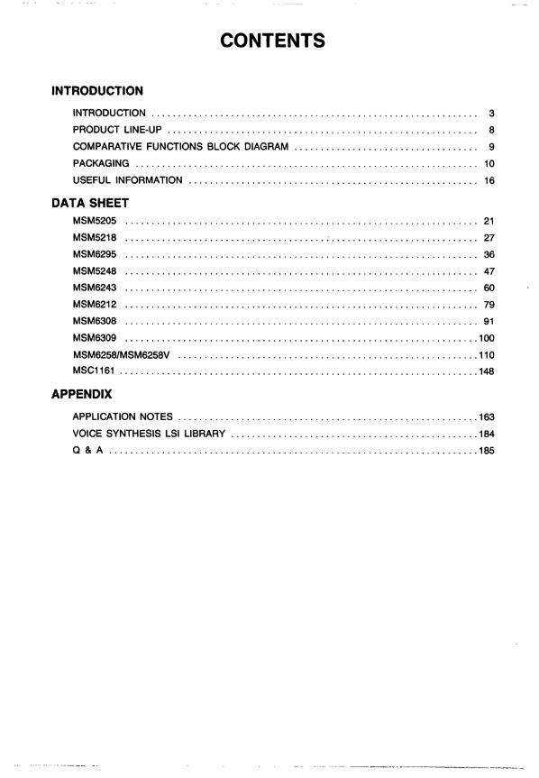
CONTENTS
INTRODUCTION
INTRODUCTION .............................................................. 3
PRODUCT LINE-UP ... . . . . . . . . . . . . . . . . . . . . . . . . . . . . . . . . . . . . . . . . . . . . . . . . . . . . . . .. 8
COMPARATIVE FUNCTIONS BLOCK DIAGRAM................................... 9
PACKAGING ................................................................. 10
USEFUL INFORMATION ....................................................... 16
DATA SHEET MSM5205 ................................................................... 21
MSM5218 ................................................................... 27
MSM6295 ................................................................... 36
MSM5248 ................................................................... 47
MSM6243 ................................................................... 60
MSM6212 ................................................................... 79
MSM6308 ................................................................... 91
MSM6309 ................................................................... 100
MSM6258/MSM6258V ......................................................... 110
MSC1161 .................................................................... 148
APPENDIX
APPLICATION NOTES ......................................................... 163
VOICE SYNTHESIS LSI LIBRARy ............................. , ................. 184
a & A ...................................................................... 185

INTRODUCTION ----,

INTRODUCTION
• The Voice Synthesis LSI In regular tape recorders where sound is stored as analog signals on magnetic
tape, the subsequent amplification of those signals to drive a speaker is referred to as sound "reproduction". It cannot be called sound "synthesis". If the amount of information stored (which is 100% in the above tape recorder) is reduced, the amount of storage medium (memory) can also be reduced for greater economy. Where the amount of information is reduced (compressed) on the basis of a certain principle, the restoration of the original sound is called "synthesis".
• Voice Synthesis Methods Voice synthesis methods can be divided into three major types:- waveform
encoding, parametric synthesis, and synthesis by rule. Each type is briefly outlined below.
(1) Waveform coding methods This type includes differential PCM (DPCM), adaptive delta modulation (ADM), and adaptive differential PCM (ADPCM). The original sound wave amplitude is sampled at fixed intervals, digitized, and the volume of data then reduced on the basis of the principles mentioned above.
(2) Parametric synthesis methods Characteristic information included in voice waveforms is extracted as parameters for synthesizing purposes. The PARCOR method is a typical example. In this method where models of the human vocalization mechanism are used, voiced and voiceless consonant sounds are discriminated, and voiced sound pitch and amplitude data is extracted together with filter characteristic of vocal tract. Voice synthesis is then achieved by passing this data to hardware consisting of digital filter circuits etc.
(3) Synthesis by rule method This synthesis method is an ideal method where groups 'of phonemes expressed by small quantities of data are skillfully linked together to reproduce any desired words. However, since further elucidation of linguistic laws taking intonation, accents, and length sounds into consideration is required to achieve a highly natural voice, this method must still be considered to be in the research stage.
• Basic ADPCM Method Oki voice synthesis LSls are based on adaptive differential PCM (ADPCM)
which is an improved form of the DPCM method. The PCM and ADPCM methods are described below.
3
.- .,., '-_.,-----
(1) Pulse code modulation (PCM) Voice waveforms and other analog data can be PCM encoded (into digital data) by sampling and quantization in S&H (sample and hold) and AD converter stages. The SIN ratio in this case is determined by the following expression
(N - 1) x 6 dB
where N is the number of output bits from the AD converter assuming that the maximum waveform amplitude is equivalent to full scale in the converter. For example, if the sampling frequency is 8 kHz and the number of AD converter output bits is 12, the required amount of data (number of bits) per second is
8 kHz x 12 bits = 96K bitslsec
This is called the bit rate. The SIN ratio is this case is obtained as
(12 - 1) x 6 = 66 dB
(2) Adaptive Differential PCM The ADPCM method was devised as a means of reducing the bit rate without sacrificing the SIN ratio too much. In this method, the amount of data is reduced by quantizing and encoding the differential (dn) between adjacent signal samples. A feature of this method is the ability to make adaptive changes to the quantization width c.n when quantizing the differential dn. (In the DPCM method, the quantization width is fixed.) In other words, c.n is enlarged when the differential dn is large, and reduced when dn is small.
(3) ADPCM analysis
4
If the input at the nth sampling pOint is Xn, and the waveform reproduction value at the (n-1 )th sampling point is Xn-1, the differential dn between the two is
1\
dn = Xn - Xn-1 (Differential calculation)
This is then encoded by the quantization width c.n at the present point of time (the nth point of time).
Ln = dnl c.n (Encoding: Ln = ADPCM data)
And if this is then quantized and the waveform subsequently reproduced,
qn = (Ln + 1/2)c.n (Quantization) 1\ 1\
Xn = Xn-1 + qn (Reproduction)
The quantization width for the next (n+ 1 )th item of data is then changed from c.n to c.n+ 1.
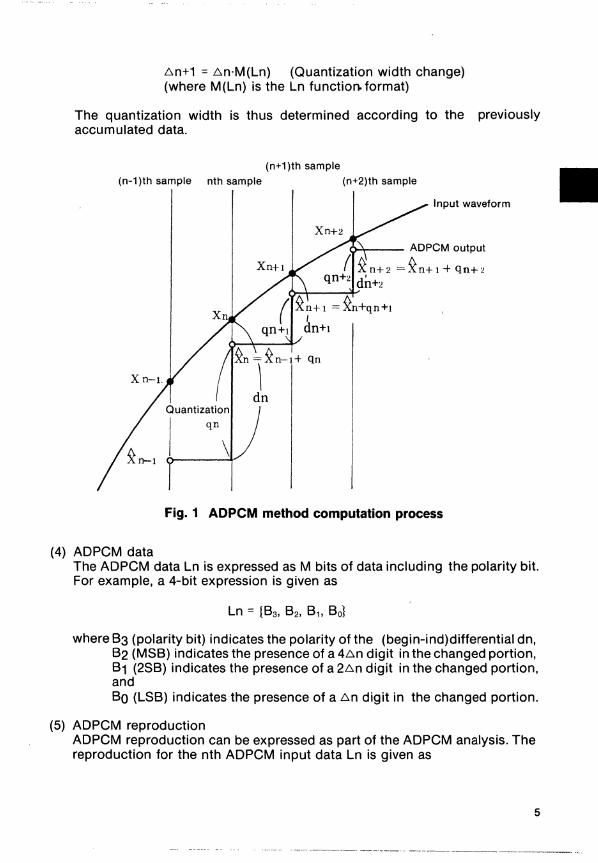
.6.n+1 = .6.n·M(Ln) (Quantization width change) (where M(Ln) is the Ln function. format)
The quantization width is thus determined according to the previously accumulated data.
(n+1 )th sample
(n-1 )th sample nth sample (n+2)th sample
Input waveform
Fig. 1 ADPCM method computation process
(4) ADPCM data The ADPCM data Ln is expressed as M bits of data including the polarity bit. For example, a 4-bit expression is given as
Ln = {B3' B2, B1, Bol
where B3 (polarity bit) indicates the polarity of the (begin-ind)differential dn, B2 (MSB) indicates the presence of a 4.6.n digit in the changed portion, B1 (2SB) indicates the presence of a 2.6.n digit in the changed portion, and BO (LSB) indicates the presence of a .6.n digit in the changed portion.
(5) ADPCM reproduction ADPCM reproduction can be expressed as part of the ADPCM analysis. The reproduction for the nth ADPCM input data Ln is given as
5
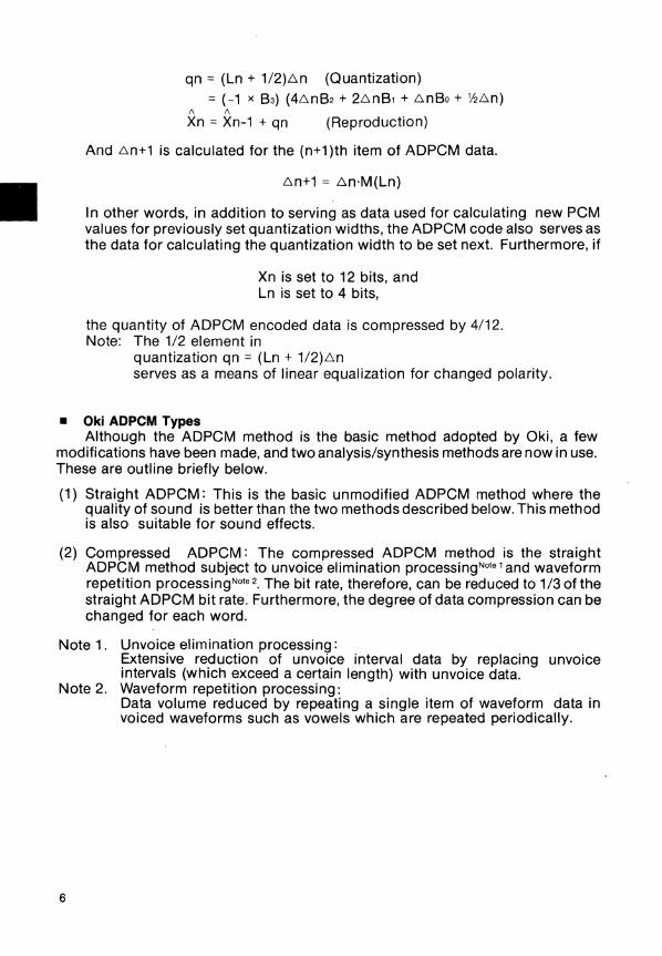
qn = (Ln + 1/2)6n (Quantization) = (-1 x B3) (46nB2 + 26nB1 + 6nBo + '126n)
A A Xn = Xn-1 + qn (Reproduction)
And 6n+1 is calculated for the (n+1 )th item of ADPCM data.
6n+1 = 6n·M(Ln)
In other words, in addition to serving as data used for calculating new PCM values for previously set quantization widths, the ADPCM code also serves as the data for calculating the quantization width to be set next. Furthermore, if
Xn is set to 12 bits, and Ln is set to 4 bits,
the quantity of ADPCM encoded data is compressed by 4/12. Note: The 1/2 element in
quantization qn = (Ln + 1/2)6n serves as a means of linear equalization for changed polarity.
• Oki ADPCM Types Although the ADPCM method is the basic method adopted by Oki, a few
modifications have been made, and two analysis/synthesis methods are now in use. These are outline briefly below.
(1) Straight ADPCM: This is the basic unmodified ADPCM method where the quality of sound is better than the two methods described below. This method is also suitable for sound effects.
(2) Compressed ADPCM: The compressed ADPCM method is the straight ADPCM method subject to unvoice elimination processingNote 1 and waveform repetition processingNote 2. The bit rate, therefore, can be reduced to 1/3 of the straight ADPCM bit rate. Furthermore, the degree of data compression can be changed for each word.
Note 1. Unvoice elimination processing: Extensive reduction of unvoice interval data by replacing unvoice intervals (which exceed a certain length) with unvoice data.
Note 2. Waveform repetition processing:
6
Data volume reduced by repeating a single item of waveform data in voiced waveforms such as vowels which are repeated periodically.
• Features of Oki Voice Synthesis LSls The major features of Oki voice synthesis LSls are summarized below.
(1) Quality and object of synthesis (i) Good quality sound with high degree of naturalness (ii) Synthesis of sound effects, musical instruments, and animal sounds also
possible
(2) Hardware (i) Easy to handle built-in ROM 1-chip devices prepared for application in
simple sets (ii) Range of voice synthesis LSls with varying built-in ROM sizes to meet
diversified market needs (iii) Low power requirements due to CMOS with low fundamental oscillating
frequency - ideal also for battery operated applications
(3) Software (i) Simple and precise analysis for broader range of user selected sounds (ii) Comprehensive range of anlilytical tools to enable synthesis to be
executed by user
Because of the fine quality of sound achieved in a wide range of applications,Oki voice synthesis LSls are used by a great many users in many different applications.
7
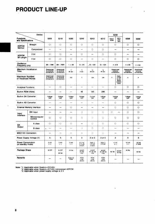
PRODUCT LINE-UP
~ Functions 5205 5218 6295 and Specifications
ADPCM Straight 0 0 0
Method Compressed - - -
ADPCM 3 bit 0 0 -
Bit Length 4 bit 0 0 0
Oscillation 384 -738K 384 -768M 1 - 5M Frequency (Hz)
Maximum Vocalization Determined Deternubed ·f Time by external by external 90 sec connectIOns connections
Maximum Number Determrned Determined
of Vocalized Words by external by external f27 connectIOns connections
Analytical Functions - 0 -
BUilt-in ROM (Kblts) - - -
BUIIt·1n DA Converter Voltage Voltage Voltage !ype Iype type
Budt-In AD Converter - - -
External Memory Interface - - 0
Input SW Input - - -
Interface Microcomputer Control 0 0 0
DA A class 0 0 0
Output B class - - -,
MSCl161 Connection - - -
Power Supply Voltage (V) 5 5 5
Power Consumption 4 mA 4 mA 5 mA (in standby mode) (-) (-) (-)
Package Shape 18 DIP 24 DIP 44 flat
32 Itat
Remarks - - External ROM
Note: ·1 Applicable when fsAMPLE = 5.5 kHz ·2 Applicable when tsAMPLE=8.2 kHz compressed ADPCM ·3 Applicable when power supply voltage IS 3 V
8
5248
0
-
0
-
10- 50K
·f 3 sec
7
-
48
Voltage type
-
-
0
0
-
u
-
3
05 rnA {1 O/<A) (05/.A)
IS-DIP 24 flat chip
ROM code
deYlce
6258
6243 6212 Stand- MPU 6308 6309 alone Inter-
I.",
0 0 0 0 0
0 0 - - -- 0 0 - -0 - 0 0 0
, ,30-t32K 30- 132K 4-8 M 4-6 M 4-6 M
., ., Determined Determined OeterlTltned 20,.., 40 sec external external external
connectionS connections connectIons
Deter· f2. 12. 7 mIned • 4
byex-ternal
connec-tionS
- - 0 0 0
192 288 - - -Current Voltage Voltage Voltage VOltage
type Iype type type !y.'
- - 0 0 0
- - 0 0 0
0 0 0 - 0 0
0 0 0 0
0 0 0 0 0
0 0 - - -
0 0 - - -3 or 5 3 or 5 5 5 5
Note 3 NOle 3 • mA 10 rnA IOmA 05 rnA 05 rnA (-) (-) (f OpAl (051,A)
40,DIP 40·DIP 4O-DIP 44 flat 44 60 flat 44, eo flat 60 flat
44 flat 60 flat
chiP chip
ROM ROM code code -- - -
deVice deVice
co
MSM5248 MSM6243 MSM6212
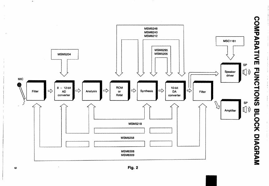
MSM6295 MSM5205
"- n /
Filter c:> AD ¢ Analysis ¢ or ¢ I Synthesis )
MIC c:J 8 - 12-bit E1 [JOM ¢ 10-bit DA
converter
h ?C:J converter RAM
r;
1 _F ~
1LJ MSM5218
MSM6258
MSM6308 MSM6309
Fig. 2
0 0 :s: ." » :D » -I -<
SP m Sp~aker I aJ») ." dnver c:
Z 0 -I -0 Z
SP en Amplifier • IT])) OJ
r 0 0 ~
C -» C) :D » i:
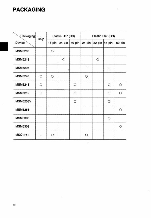
PACKAGING
~ Plastic DIP (RS) Plastic Flat (GS)
Chip Device 18 pin 24 pin 40 pin 24 pin 32 pin 44 pin 60 pin
MSM5205 0
MSM5218 0 0
MSM6295 0 . MSM5248 0 0 0
MSM6243 0 0 0 0
MSM6212 0 0 0 0
MSM6258V 0 0
MSM6258 0
MSM6308 0
MSM6309 0
MSC1161 0 0 0
10
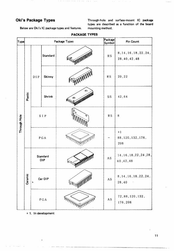
Oki's Package Types
Below are Oki's IC package types and features.
Through-hole and surface-mount IC package types are described as a function of the board mounting method.
PACKAGE TYPES
Type Package Types Package Pin Count Symbol
~ 8,14,16,18,22,24, Standard RS
28,40,42,48
DIP Skinny ~ RS 20,22
()
~ .;:; Shrink SS 42,64 ..
'" 1i:
., SIP ~ RS 8 (5 :I: -§, ::l e
Q .s:: I- *1
PGA - 88,120,132.176,
208
Standard ~ 14,16.18,22,24,28. AS
DIP 4tl,42,48
()
~ 8,14,16,18.22,24. ·E '" Cer DIP AS ~ , 28,40
~ 72,88,120,132, PGA ~ AS
176,208
* 1. In development
11
12
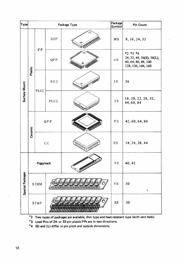
Type Package Type Package Pin Count Symbol
SOP MS 8,16,24,32
FP *2 *3 *4
QFP GS 24,32,44, 56(S), 56(L), 60,64,80,88,100
to) 128, 136, 144, 160 .;::l .. OJ
a:::
... sOJ c: JS 26 :::J 0 ~ PLCC
Q> to) OJ 't: 18,20,22,28,32, :::J PLCC JS II) 44,68,84
QFP FS 42,60,64,80
.!:! E ~ Q>
U
CC ES 14,24,28,44
Piggyback VS 40,42
& ~------.-------l-------~~------------4-----+---______________ ~ OJ -" ~ (ij
SIMM YS 30
l II) ~------4-------------------------------4-----+-----------------~
SIMP KS 30
*2 Two types of packages are available, thin type and heat· resistant type (with vent hole).
*3 Lead Pins of 24- or 32-pin plastic FPs are in two directions. *4 (5) and (L) differ in pin pitch and outside dimensions.
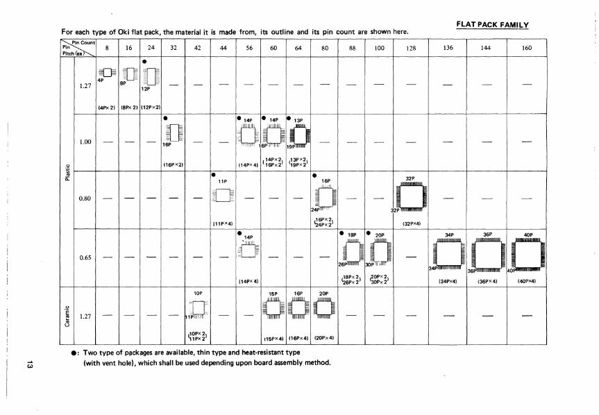
FLAT PACK FAMILY For each type of Oki flat pack, the material it is made from, its outline and its pin count are shown here.
~t Pin 8 16 24 32 42 44 56 60 64 80 88 100 128 136 144 160 Pitch Gnm
• 0 {] i] -
4P 1.27 SP - - - - - - - - - - - - -
12P
(4PX21 (SPX21 (12Px21
• • 14P • 14P • 13P
1.00 - - -[]
- - :OlD 16P 10 - - - - - - -
u (16P X 21 114px 41 ( ~:~~~I (~~~;~I .~ • • 0: lIP 16P 32P
0.80 - - - - - [J - - -2D
- - ~O - - -
J11p X 41 ~~~~~I (32PX41
• • lSP • 20P 34P 36P 40P 14P
20 0 0 D ~O 0.65 - - - - - -,:U
- - - 3O~'111I"1'" ~ -
(14PX41 ~~~~~I sg~~~1 (34PX41 (36P X 41 (40PX41
lOP 15P 16P 20P
;CJ 0 0 0 u -
'E 1.27 - - - - - - - -- - - - -~ II
"
I u
(:~~~~I 115PX41 (16Px41 (20Px41
e: Two type of packages are available, thin type and heat-resistant type ..... W
(with vent hole), which shall be used depending upon board assembly method .
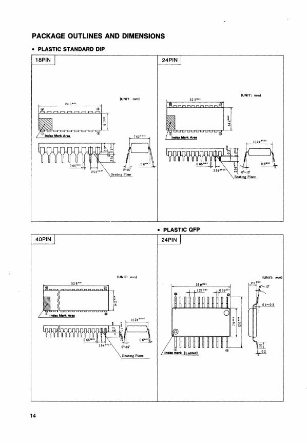
PACKAGE OUTLINES AND DIMENSIONS
• PLASTIC STANDARD DIP
18PIN
(UNIT. mml
B 254:!:02S O~15°
Seabng Plan'!
40PIN
(UNIT: mm)
Seating Plane
14
24PIN
(UNIT: mm)
.. ~~ )~~r\~()~,~~~r-~~~~ ,
• PLASTIC QFP
24PIN
~ ~ NI 0·-15' Seatm Plane
(UNIT: mml
22±02
0·-10·
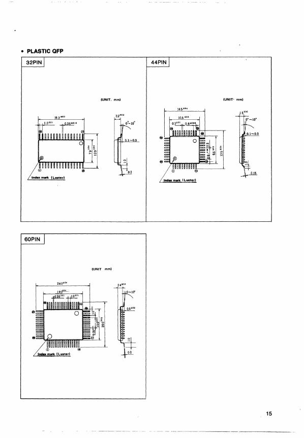
• PLASTIC QFP
32PIN 44PIN
(UNIT. mm) (UNIT' mm)
22;t02 15%02
0.1-0.3
In"" mark C LUlter. Index mark C LUlter)
60PIN
(UNIT mm)
15
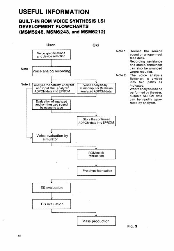
USEFUL INFORMATION BUILT-IN ROM VOICE SYNTHESIS LSI DEVELOPMENT FLOWCHARTS (MSM,5248, MSM6243, and MSM621 2)
16
User
Analyze the data by analyzer and input the analyzed
ADPCM data into EPROM
Oki
Note 1. Record the source sound on an open-reel tape deck. Recording assistance and studio/announcer can also be arranged where required.
Note 2. The voice analysis flowchart is divided into two paths as indicated. Where analysis is to be performed by the user, suitable ADPCM data can be readily generated by analyzer.
Fig. 3
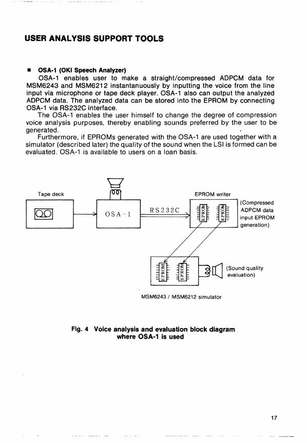
USER ANALYSIS SUPPORT TOOLS
• OSA·1 (OKI Speech Analyzer) OSA-1 enables user to make a straight/compressed ADPCM data for
MSM6243 and MSM6212 instantanuously by inputting the voice from the line input via microphone or tape deck player. OSA-1 also can output the analyzed ADPCM data. The analyzed data can be stored into the EPROM by connecting OSA-1 via RS232C interface.
The OSA-1 enables the user himself to change the degree of compression voice analysis purposes, thereby enabling sounds preferred by the user to be generated.
Furthermore, if EPROMs generated with the OSA-1 are used together with a simulator (described later) the quality of the sound when the LSI is formed can be evaluated. OSA-1 is available to users on a loan basis.
Tape deck
OSA -1 RS232C
EPROM writer
(Compressed ADPCM data input EPROM
'--:>''----r-----' generation)
rr1 (Sound quality L1-J evaluation)
MSM6243/ MSM6212 simulator
Fig.4 Voice analysis and evaluation block diagram where OSA-1 is used
17
• Speech Analyzer The speech analyzer set using MSM5218RS is used to make an ADPCM
data on real-time basis by inputting voice from microphone or tape deck player etc. Analyzed data is stored in a built-in RAM, and can be written into an EPROM by a built-in EPROM writer.
This EPROM can be used as the voice simulator's data or as ROM data for MSM5248 etc. For further details, please contact
Nihon Denso Kogyo Co., Ltd. 3-14-19 Shibaura, Minato-ku, Tokyo, Japan TEL. (03) 452-2351
• MSM5248 Simulator The MSM5248 simulator has the same functions as the MSM5248. When
the EPROM, in which the analyzed data is stored, is mounted on this simulator, this simulator can synthesize the same quality voice data as that of MSM5248.
• MSM6243 Simulator, MSM6212 Simulator When the EPROM, in which the analyzed data by using OSA-1 is stored, is
mounted on the simulator these simulators can synthesize the same quality voice data as that of MSM6243, MSM6212 respectively.
18
DATA SHEET---------.

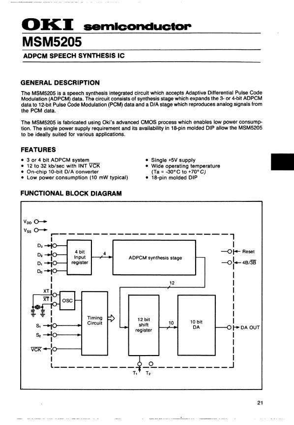
OKI semiconductor MSM5205 ADPCM SPEECH SYNTHESIS IC
GENERAL DESCRIPTION
The MSM5205 is a speech synthesis integrated circuit which accepts Adaptive Differential Pulse Code Modulation (ADPCM) data. The circuit consists of synthesis stage which expands the 3- or 4-bit ADPCM data to 12-bit Pulse Code Modulation (PCM) data and a D/A stage which reproduces analog signals from the PCM data.
The MSM5205 is fabricated using Oki's advanced CMOS process which enables low power consumption. The single power supply requirement and its availability in 18-pin molded DIP allow the MSM5205 to be ideally suited for various applications.
FEATURES
• 3 or 4 bit ADPCM system • 12 to 32 kb/sec with INT VCK • On-chip 10-bit D/ A converter • Low power consumption (10 mW typical)
FUNCTIONAL BLOCK DIAGRAM
Vee 0-Vss 0-
• Single +5V supply • Wide operating temperature
(Ta = -30°C to +70° C) • 18-pin molded DIP
,---------------------, ~~ I D -t 4 bit 4 -{) t+- Reset
2 I Input ADPCM synthesis stage 1 D, ~ register --01- 48/38
~~ I 1 12 1
XT 1 1 XTI I
D ;..;1 - - I Timing
Circuit 10
I 1 1
5, ~IO---~ 12 bit shift
register
10 bit DA I-DA OUT
S.-tlo---~ I
VCK -l:O-----I I L..-_---' L _________ _
1 1 I 1 _C2.- _________ J
21
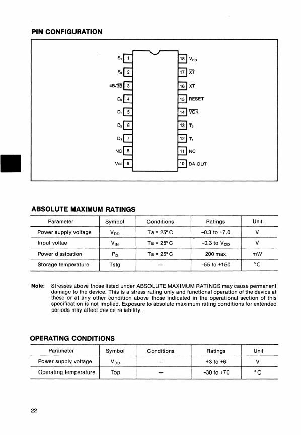
PIN CONFIGURATION
18 Vee
XT
XT
RESET
VCK
T2
T,
NC
10 DA OUT
ABSOLUTE MAXIMUM RATINGS
Parameter Symbol Conditions Ratings Unit
Power supply voltage Voo Ta = 25° C -0.3 to +7.0 V
Input voltae V1N Ta = 25°C -0.3 to Voo V
Power dissipation Po Ta = 25°C 200 max mW
Storage temperature Tstg - -55 to +150 °C
Note: Stresses above those listed under ABSOLUTE MAXIMUM RATINGS may cause permanent damage to the device. This is a stress rating only and functional operation of the device at these or at any other condition above those indicated in the operational section of this specification is not implied. Exposure to absolute maximum rating conditions for extended periods may affect cl€vice raliability.
OPERATING CONDITIONS
Parameter Symbol Conditions Ratings Unit
Power supply voltage Voo - +3 to +6 V
Operating temperature Top - -30 to +70 °C
22
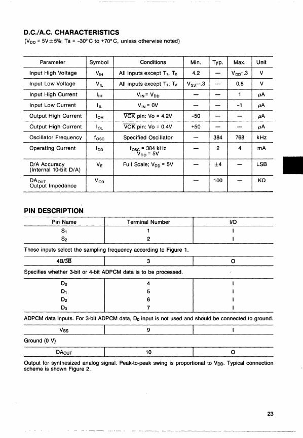
D.C'!A.C. CHARACTERISTICS (VDD = 5V±5%; Ta = -30°C to +70°C, unless otherwise noted)
Parameter Symbol Conditions Min.
Input High Voltage VIH All inputs except T" T2 4.2
Input Low Voltage VIL All inputs except T" T2 Vss-·3
Input High Current IIH VIN = VDD -Input Low Current IlL VIN = OV -
Output High Current IOH VCK pin: Vo = 4.2V -50
Output High Current IOL VCK pin: Vo = 0.4V +50
Oscillator Frequency fosc Specified Oscillator -Operating Current IDD fosc = 384 kHz -
VDD = 5V
D/A Accuracy VE Full Scale; VDD = 5V -(Internal 10-bit D/A)
DAoUT VOR -Output Impedance
PIN DESCRIPTION
Pin Name Terminal Number
2
These inputs select the sampling frequency according to Figure 1.
4B/3B 3
Specifies whether 3-bit or 4-bit ADPCM data is to be processed.
4
5
6 7
Typ. Max. Unit
- VDD+·3 V
- 0.8 V
- 1 JlA
- -1 JlA
- - JlA
- - JlA
384 768 kHz
2 4 mA
±4 - LSB
100 - KO
1/0
o
ADPCM data inputs. For 3-bit ADPCM data, Do input is not used and shduld be connected to ground.
Vss 9
Ground (0 V)
DAouT 10 o Output for synthesized analog signal. Peak-to-peak swing is proportional to Voo. Typical connection scheme is shown Figure 2.
23
PIN DESCRIPTION (continued)
12
13
IC test pins used at the factory for testing purposes only. During normal operations, Tl is grounded and T2 is left open.
Pin Name Terminal Number 1/0
VCK 14 o This pin outputs a signal whose frequency is equal to the sampling frequency selected by the S1, S2 inputs. See note *1.
RESET 15
An active high input which initializes the internal circuitry. Internally, the reset pulse is synchronized with the VCK signal. To be effective, it must be true for at least twice VCK time.
XT XT
16
17
1/0
1/0
Oscillator input and output for a 384 kHz crystal or ceramic resonator (Figure 3).
'Voo 18
Power supply pin (Typical + 5 V)
24
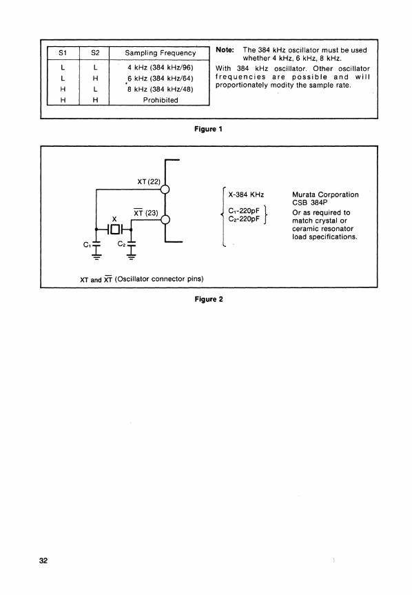
S1 S2
L L
L H
H L
H H
Sampling Frequency
4 kHz (384 kHz/96)
6 kHz (384 kHz/64)
8 kHz (384 kHz/48)
Prohibited See Note *1
Note: "1 The 384 kHz oscillator must be used whether 4 kHz, 6 kHz, 8 kHz.
Figure 1 Functional table
DAOUT
--~~O ~I LPF H>1 AMP Speaker
Cut off frequency fc of LPF should be related to the selected sampling frequency f sample by,
fc = f sample/2 x 0.85
Sound quality is strongly dependent on the sharpness of thE' low pass filter.
*If the 5205 is sent a stream of ADPCM data that causes greater than full scale output, the D/A output will wrap around: +5 0.0 +5.
Figure 2
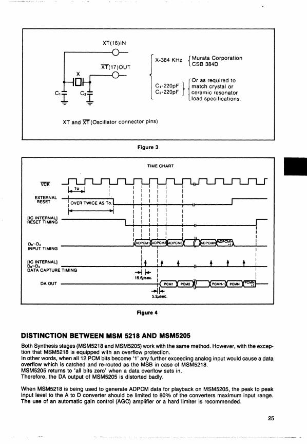
EXTERNAL RESET
XT(16)IN
X-384 KHz {MUrata Corporation CSB 3840
C,-220pF match crystal or (Or as required to
C2-220PF} ceramic resonator load specifications.
XT and X1(Osciliator connector pins)
Figure 3
TIME CHART
I..!2-J : I
! OVER TWICE AS TO.!-! --...;..4_.-_-i--...;.-illl-------1
I- "I [IC INTERNALI ________ .....
RESET TIMING L...-+-...;.. ..... -4_I-_ ..... _~III--------_!
00-0, INPUT TIMING
I I I I
gc INTERNAL] i t I t t t t t 0-0, _____________ ....j.,~ __ ~IL----L--~I!~I-~---~-----L-~--
DATA CAPTURE TIMING -..j j..- I I
15.6psec. I~~ ---------------~I~~··· ...
-..jj;: oAOUT
5.2lAsec.
Figure 4
DISTINCTION BETWEEN MSM 5218 AND MSM5205 Both Synthesis stages (MSM5218 and MSM5205) work with the same method. However, with the exception that MSM5218 is equipped with an overflow protection. In other words, when all 12 PCM bits become '1' any further exceeding analog input would cause a data overflow which is catched and re-routed as the MSB in case of MSM5218. MSIjII5205 returns to 'all bits zero' when a data overflow sets in. Therefore, the OA output of M~M5205 is distorted badly.
When MSM5218 is being used to generate AOPCM data for playback on MSM5205, the peak to peak input lel1el to the A to 0 converter should be limited to 80% of the converters maximum input range. The use of an automatic gain control (AGC) amplifier or a hard limiter is recommended.
25
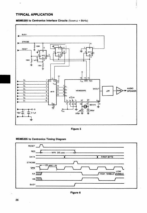
TYPICAL APPLICATION
MSM5~5 to Centronics Interface Circuits (fSAMPLE = 8kHz)
BUSY
STROBE
RESET
lOOK
lOOk
18 14 15 D. Voo VCR RES D, 5
D, 3 7 D, 1 12 6 D, DAOUT
6 4019 11 5 D, MSM5205RS LPF
D,
D.
D, 4 10 400
2 D, 15
Vss a
':"
Voo
Figure 5
MSM5205 to Centronics Timing Diagram
RESET~~ ________________________________________ ___
RES ~"'.---MIN 250psec--_~I'----------------DATA _________ I~ ___________ I~~F~IR~S~T~B~Y~T~E~ __ _
STROBE ____ ~---------J
I \~ ___ ..J'--BUSy ____________________ --JJ
Figure 6
26
AUDIO SPEAKER
OKI 5eft1iconductor
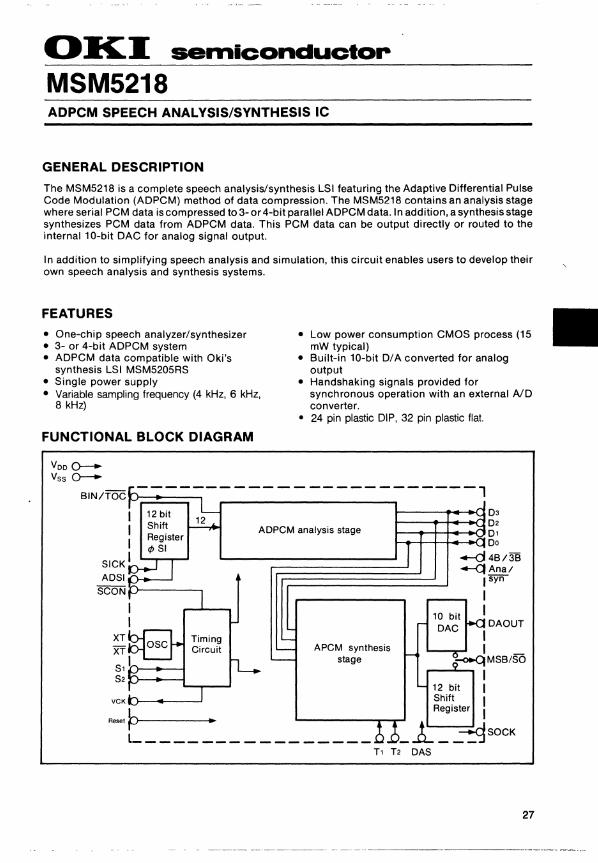
MSM5218 ADPCM SPEECH ANALYSIS/SYNTHESIS IC
GENERAL DESCRIPTION
The MSM5218 is a complete speech analysis/synthesis LSI featuring the Adaptive Differential Pulse Code Modulation (ADPCM) method of data compression. The MSM5218 contains an analysis stage where serial PCM data is compressed to 3- or 4-bit parallel ADPCM data. In addition, a synthesis stage synthesizes PCM data from ADPCM data. This PCM data can be output directly or routed to the internal 10-bit DAC for analog signal output.
In addition to simplifying speech analysis and simulation, this circuit enables users to develop their own speech analysis and synthesis systems.
FEATURES
• One-chip speech analyzer/synthesizer • 3- or 4-bit ADPCM system • ADPCM data compatible with Oki's
synthesis LSI MSM5205RS • Single power supply • Variable sampling frequency (4 kHz, 6 kHz,
8 kHz)
FUNCTIONAL BLOCK DIAGRAM
Voo 0---Vss 0----
• Low power consumption CMOS process (15 mW typical)
• Built-in 10-bit 0/ A converted for analog output
• Handshaking signals provided for synchronous operation with an external AID converter.
• 24 pin plastic DIP, 32 pin plastic fiat.
BIN/TOC ------------------------,
ADSI....,.-__
SCaN l.r-----,
XT
VCK
Rese1 p .-
ADPCM analysis stage
APCM synthesis stage
L _______________ _
t---___ _+<.l D3 t-----1t---+ __ _+<""l D2 t----1>-1-+ __ _+<~ D 1
HH-I-+---<:lDo ---d 4B/38 -+--Q Anal
10 bit DAC
I syn
I I
DAOUT
I I _
~MS8/S0 ~-.:L..., I
12 bit Shift Register
I I I
_.f. __ ~ SOCK
T1 T2 DAS
27
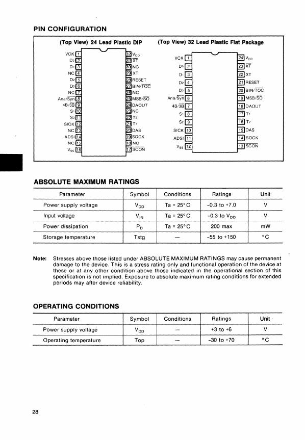
PIN CONFIGURATION
(Top View) 24 Lead Plastic DIP (Top View) 32 Lead Plastic Flat Package
ABSOLUTE MAXIMUM RATINGS
Parameter Symbol Conditions Ratings Unit
Power supply voltage VDD Ta = 25°C -0.3 to +7.0 V
Input voltage VrN Ta = 25°C -0.3 to VDD V
Power dissipation PD Ta = 25°C 200 max mW
Storage temperature Tstg - -55 to +150 °C
Note: Stresses above those listed under ABSOLUTE MAXIMUM RATINGS may cause permanent damage to the device. This is a stress rating only and functional operation of the device at these or at any other condition above those indicated in the operational section of this specification is not implied. Exposure to absolute maximum rating conditions for extended periods may after device reliability.
OPERATING CONDITIONS
Parameter Symbol Conditions Ratings Unit·
Power supply voltage VDD - +3 to +6 V
Operating temperature Top - -30 to +70 °C
28
D.CJ A.C. CHARACTERISTICS (Voo =5V±5%, Ta= -30oe to + 70oe, unless otherwise noted)
Parameter Symbol Conditions Min. Typ. Max. Unit
Input High Voltage VIH All input except 4.2 - - V T1, T2
Input Low Voltage VIL All inputs except - - 0.8 V T1, T2
Input High Current(1) IIH VIN = Voo - - 1 JiA
Input Low Current IlL VIN = OV - - -1 JiA
Output High Current IOH SCON, VCK, SOCK, -50 - - JiA MSBJSO, 00-03
Vo = 4.2V
Output Low Current IOL SCON~CK SOCK, 50 - - JiA MSBJ ,00 - 03
Vo = OAV
Oscillator Frequency fosc Specified Oscillator - 384 768 kHz
Operating Current 100 fVCK = 8 kHz - 3 6 mA Operating Current 100 fVCK = 16 kHz - 6 12 mA
DA. OUT Output Impedance VOR 100 - kO
DJ A Accuracy Ve Full Scale - ±4 - LSB (Internal 10-bit OJ A) Voo = +5V
SICK Clock Frequency fSICK - - 500 kHz
Input High current (2) IIH2 VIN = Voo Note 1 20 - 400 JiA
Note1: Applicable for Reset
29

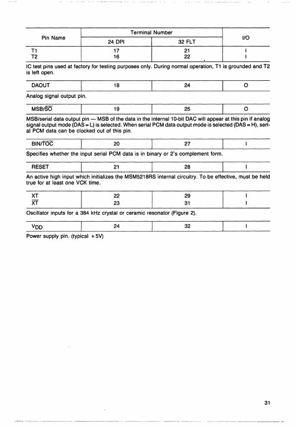
PIN DESCRIPTION
Terminal Number Pin Name
24 DIP 32 FLT I/O
VCK 1 1 0
This pin outputs a signal whose frequency is equal to the sampling frequency selected by S1, S2 inputs.
Do D1 D2 D3
2 3 4 5
2 3 5 6
Data I/O port for the ADPCM data. For 3-bit ADPCM data, Do input is not used.
ANAISYN 6 8
I/O I/O I/O I/O
I/O
Analyze/synthesize function selector. Controls data I/O port direction. When high, data I/O are outputs and simultaneous analysis and synthesis occur. When low, data I/O are inputs and no analysis occurs.
4B/3B 7 9
Specifies whether 3-bit or 4-bit ADPCM data is to be used. High = 4-bit.
8 9
10 11
These inputs select the sampling frequency according to figure 1.
SICK 10 12
o
Clock input for clocking in serial PCM data from an external ADCinto the internal 12-bit shift resister.
ADSI 11 14
Serial PCM data input.
VSS 12 16
Ground (OV)
SCON 13 17 0
Output which signals the start of conversion.
SOCK 14 19 0
When serial PCM data output mode is selected (DAS = H), this pin provides a 192 kHz signal which is synchronized with the output of the serial PCM data through the MSB/SO pin. Each bit of the 12-bit PCM data will be valid before the positive edge of this 192 kHz signal.
DAS 15 20 o Selector for analog signal output (DAS = L), or serial PCM data output (DAS = H).
30
T1 T2
Pin Name 24 DPI
17 16
Terminal Number
32 FLT
21 22
1/0
Ie test pins used at factory for testing purposes only. During normal operation, T1 is grounded and T2 is left open.
DAOUT 18 24 o Analog signal output pin.
MSB/SO 19 25 o MSB/serial data output pin - MSB of the data in the internal10-bit DAC will appear at this pin if analog signal output mode (DAS = L) is selected. When serial PCM data output mode is selected (DAS = H), serial PCM data can be clocked out of this pin.
BINITOC 20 27
Specifies whether the input serial PCM data is in binary or 2's complement form.
RESET 21 28
An active high input which initializes the MSM5218RS internal circuitry. To be effective, must be held true for at least one VCK time.
XT XT
22 23
29 31
Oscillator inputs for a 384 kHz crystal or ceramic resonator (Figure 2).
VDD 24 32
Power supply pin. (typical + 5V)
31
S1
L
L
H
H
32
S2
L
H
L
H
Sampling Frequency
4 kHz (384 kHzl96)
,6 kHz (384 kHzl64)
8 kHz (384 kHzl48)
Prohibited
Note: The 384 kHz oscillator must be used whether 4 kHz, 6 kHz, 8 kHz.
With 384 kHz oscillator. Other oscillator frequencies are possible and will proportionately modity the sample rate.
Figure 1
X-384 KHz
C,-220pF } C2-220pF
Murata Corporation CSB 384P Or as required to match crystal or ceramic resonator load specifications.
Xl and XT (Oscillator connector pins)
Figure 2
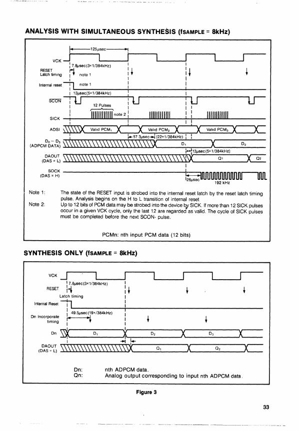
ANALYSIS WITH SIMULTANEOUS SYNTHESIS (fSAMPLE = 8kHz)
I- 125IJsec--+<~1
VCK .J I r-I ---:" __ -1
: 7.8IJsec(3x 1/384kHz) I I
RESET!1 + : I Latch timing I note 1 I t
I
Internal reset ""1lL_no_te_1 _____ t--______ ~:'_ _________ _ I 13iJSec(5x1/384kHz) I
SCONilJ I ~
SICK I 111111111111 note 2 111111111111 I I I
AOSI m Valid PCM, ~ Valid PCM, ~ Valid PCM3 c=x=
u u 111111111111
I !--57 3iJSec..j (22x1/384kHz) :
(AOPCJ'~;T~) \\\\\\\\\\\\\\\\\\\\\\\\\SX 0, XI... ___ O';"" __ r-: 13lJsec(5x 1/384kHz)
(g:so=u~) t"T\\""\\~\\M"\'\""I\\~\"r"'I\\~\"'t""O\\~\"'t""O\\i"T\~\\\'I:\~\'r:\\~\"'t""O\\i"T\'\'\\\'I:\~\'r:'3~I\X 0, I
SOCK -----------------~~nnnnnnnnnnn~nn (OAS = H) I;:::jJUUUUUUUUUUU UUL
iJSec 192 kHz
Note 1:
Note 2:
The state of the RESET input is strobed into the internal reset latch by the reset latch timing pulse. Analysis begins on the H to L transition of internal reset Up to 12 bits of PCM data may be strobed into the device bl SICK. If more than 12 SICK pulses occur in a given VCK cycle, only the last 12 are regarded as valid. The cycle of SICK pulses must be completed before the next SCON- pulse.
PCMn: nth input PCM data (12 bits)
SYNTHESIS ONLY (fSAMPLE = 8kHz)
VCK -'
17.8iJSec(3x1/384kHz) I
RESET 11 : t Latch timing I
Internal Reset -n : I I I 49.5iJSec (19x/384kHz) I
On Incorporate I"' .1 I timing I' I
I 1_------..... ,..--------."..--On ~ 0, ¥ 0, X 0 3 x\.. __
I +l '-
(O~~o=U~ \\\\\\\\\\\\\\\\\\\\X~====O=,=====X\.. __ ..=;O,:...... __ x== On: nth AOPCM data. Qn: Analog output corresponding to input nth AOPCM data.
Figure 3
33
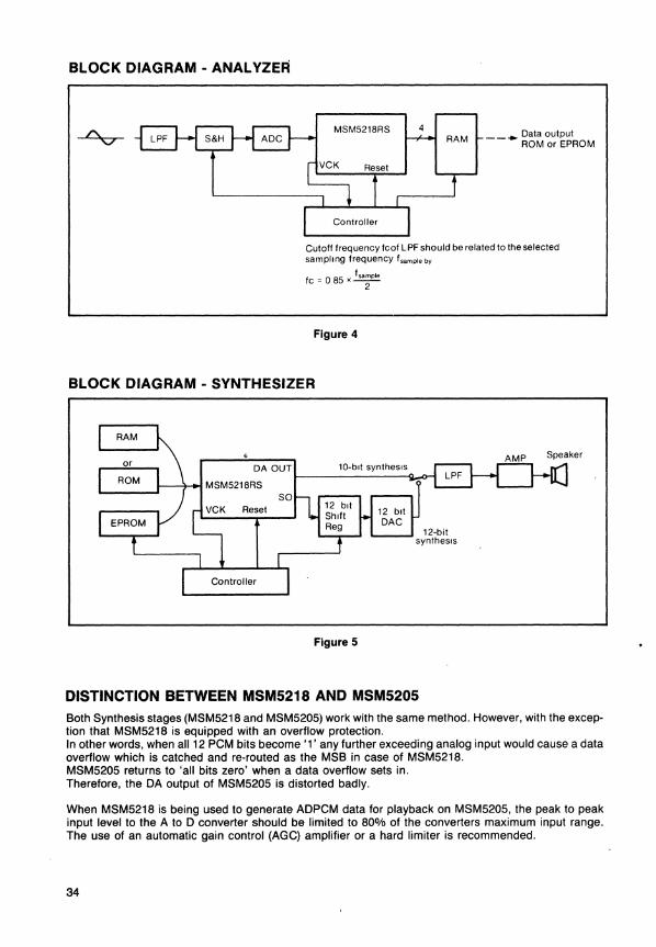
BLOCK DIAGRAM - ANALYZER
v __ +- Data output ROM or EPROM
Cutoff frequency fcof LPF should be related to the selected sampling frequency f sample by
fc = 085 x fsample 2
Figure 4
BLOCK DIAGRAM - SYNTHESIZER
Figure 5
DISTINCTION BETWEEN MSM5218 AND MSM5205 Both Synthesis stages (MSM5218 and MSM5205) work with the same method. However, with the exception that MSM5218 is equipped with an overflow protection. In other words, when all 12 PCM bits become '1' any further exceeding analog input would cause a data overflow which is catched and re-routed as the MSB in case of MSM5218. MSM5205 returns to 'all bits zero' when a data overflow sets in. Therefore. the DA output of MSM5205 is distorted badly.
When MSM5218 is being used to generate ADPCM data for playback on MSM5205, the peak to peak input level to the A to 0 converter should be limited to 80% of the converters maximum input range. The use of an automatic gain control (AGC) amplifier or a hard limiter is recommended.
34
W 0"1
1M
+ +
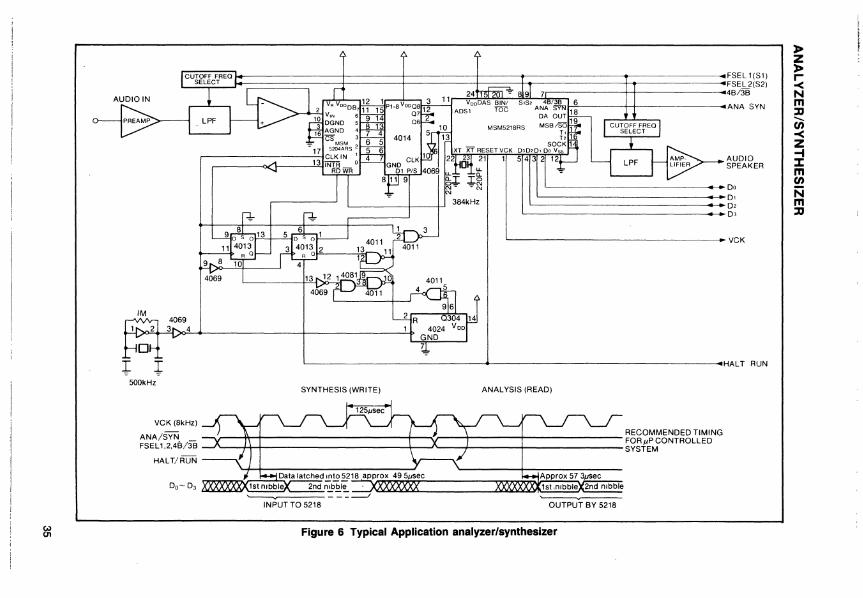
~ ~ :"'"'''' 1 CU~~E:rfTREQ I: I J ---=~7~(S2) I ~ ~ ~4 ~;o 20 ",,- ~;- 7Lo,/6 I I ANA SYN
2 VA VOD087 ~~ 10 ~~ND 6 9
t~ AGND ~ CS MSM 6
17 5204ARS 2 5 ~-----------'-'-ICLKIN 1 4 ~ ____ <X1-___ 1,-,3'lIN~ \VA 0
AUDIO SPEAKER
'II .. Do 'II --01 'II .. 02 II • 03
L-________________________________ -.~ VCK
L----------------~~--------------------~.HALT RUN
500kHz SYNTHESIS (WRITE) ANALYSIS (READ)
VCK (8kHz)
ANA/SYN )} It) ? RECOMMENDED TIMING FSEL1,2,4B/3B::::::X 1 x FOR/JPCONTROLLED
HAL TlRUN ___ I SYSTEM
.!!l!9g18 approx 495tJSec Do- 0 3 1st nibble 2nd n.!!'2!~ =:xxxxxxxx 1st ,nibble 2nd nibble
-------.....-- - - -~ INPUT TO 5218
~
OUTPUT BY 5218
Figure 6 Typical Application analyzer/synthesizer
>Z >r -< N m ::D en -< z -I ~ m CJ)
N m ::D
OKI semiconductor
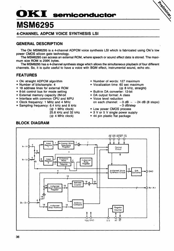
MSM6295 4-CHANNEL ADPCM VOICE SYNTHESIS LSI
GENERAL DESCRIPTION
The Oki MSM6295 is a 4-channel ADPCM voice synthesis LSI which is fabricated using Oki's low power CMOS silicon gate technology.
The MSM6295 can access an external ROM, where speech or sound effect data is stored. The maximum size ROM is 256K bytes.
The MSM6295 has a 4-channel synthesis stage which allows the simultaneous playback of four different channels. So, it is quite useful to have a voice with BGM effect, instrumental sound, echo etc.
FEATURES
• Oki straight ADPCM algorithm • Number of bits/sample: 4 • 18 address lines for external ROM • 8-bit control bus for mode setting • External memory capacity 2M-bit • Interface with common CPU and MPU • Clock frequency: 1 MHz and 4 MHz • Sampling frequency: 6.4 kHz and 8 kHz
(@ 1 MHz clock) 25.6 kHz and 32 kHz (@ 4 MHz clock)
BLOCK DIAGRAM
14-17
10-13
• Number of words: 127 maximum • Vocalization time: 60 sec maximum
(@ 8 kHz, straight) • Built-in DA converter: 12-bit • DA output format: A class • Voice level reduction
on each channel: -3 dB - -24 dB (8 steps) -3 dB/step
• Low power CMOS process • 3 V or 5 V si'\9le power supply • 44 pin plastic flat package
4·channel VOIce ,-___ -/'--_________ ++-_.j SyntheSIS CIrCUIt DAO
18
18
'-+--------.,----+--0 Ao-A17
00-070--+-1
VOOGNO 88
36
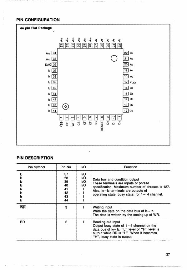
PIN CONFIGURATION
44 pin Flat Package
'" ... '" N e 0> ~ < ~ .:£ < < < < < < <{
A'6 A4
A'7 0 Aa
A2
10 A,
11 Ao
12 Voo Ia 07
14 06
15 05
16 @) 04
17 Oa
en 0 II: en I- I~ en l- e Ci 0 en II: 3: () X en w 0 > en
w II:
PIN DESCRIPTION
Pin Symbol Pin No. 110 Function
10 37 1/0 h 38 110 Data bus and condition output 12 39 110 These terminals are inputs of phrase 13 40 1/0 specification. Maximum number of phrases is 127. 14 41 I Also, 10 -13 terminals are outputs of Is 42 I operating state, busy state, for 1 - 4 channel. Is 43 I 17 44 I
WR 3 I Writing input Write the data on the data bus of 10 -17. The data is written by the setting-up of WR.
-RD 2 I Reading out input
Output busy state of 1 - 4 channel on the data bus of 10-13. "L" level or "H" level is output while RD is "L". When it becomes "H", busy state is output.
37
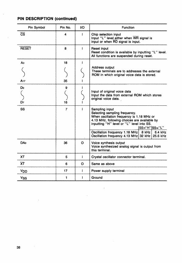
PIN DESCRIPTION (continued)
Pin Symbol Pin No. I/O Function
CS 4 I Chip selection input Input "L" level either when WR signal is input or when RD signal is input.
RESET 8 I Reset input Reset condition is available by inputting "L" level. All functions are suspended during reset.
Ao 18 I
S S S Address output These terminals are to addresses the external ROM in which original voice data is stored.
A17 35 I
Do 9 I
S S S Input of original voice data Input the data from external ROM which stores original voice data.,
07 16 I
SS 7 I Sampling input Selecting sampling frequency. When oscillation frequency is 1.18 MHz or 4.13 MHz, following choices are available by inputting "H" level or "L" level into SS.
SS="H" SS="L" Oscillation frequency 1 .18 MHz 8 kHz 6.4 kHz Oscillation frequency 4.13 MHz 32 kHz 25.6 kHz
DAo 36 0 Voice synthesis output Voice synthesized analog signal is output from this terminal.
XT 5 I Crystal oscillator connector terminal.
XT 6 0 Same as above
VDD 17 I Power supply terminal
VSS 1 I Ground
38
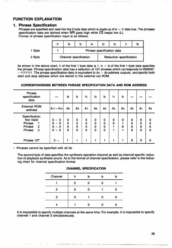
FUNCTION EXPLANATION
1. Phrase Specification Phrases are specified and read into the 2 byte data which is made up of 10 - 17 data bus. The phrases specification data are latched when WR goes high while CS keeps low (L). Format of phrase specification input is as follows.
17 Is J 15 1 14 I 13 I 12 J 11 I 1 Byte
2 Byte
1 Phrase specification data
Channel specification I Reduction specification
10
As shown in the above chart, 17 of the first 1 byte data is 1. 10 - Is of the first 1 byte data specifies the phrase. Phrase specification data has a selection of 127 phrases which corresponds to 0000001 -1111111. The phrase specification data is equivalent to A3 - A9 address outputs, and specify both start and stop address which are stored in the external out ROM.
CORRESPONDENSE BETWEEN PHRASE SPECIFICATION DATA AND ROM ADDRESS
Phrase specification - Is 15 14 13 12 11 10 - - -
data
External ROM A17-A10 A9 As A7 As A5 A4 A3 A2 A1 Ao address
Specification Not Valid 0-0 0 0 0 0 0 0 0 0 0 0
Phrase 1 0-0 0 0 0 0 0 0 1 0 0 0 Phrase 2 0-0 0 0 0 0 0 1 0 0 0 0 Phrase 3 0-0 0 0 0 0 0 1 1 0 0 0
Phrase 127 0- 1 1 1 1 1 1 1 0 0 0
• Phrases cannot be specified with all Os.
The second byte of data specifies the synthesis operation channel as well as channel specific reduction of playback synthesis sound. As to the format of channel specification, please refer to the following chart for channel specification format.
CHANNEL SPECIFICATION
Channel 17 Is 15 14
o o o
2 o o o
3 o o o
4 o o o
It is impossible to specify multiple channels at the same time. For example, it is impossible to specify channel 1 and channel 3 simultaneously.
39
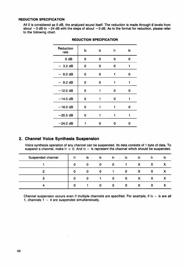
REDUCTION SPECIFICATION
2.
40
All 0 is considered as 0 dB, the analyzed sound itself. The reduction is made through 8 levels from about - 3 dB to - 24 dB with the steps of about - 3 dB. As to the format for reduction, please refer to the following chart.
REDUCTION SPECIFICATION
Reduction 13 12 11 10 rate
o dB 0 0 0 0
- 3.2 dB 0 0 0 1
- 6.0 dB 0 0 1 0
- 9.2 dB 0 0 1 1
-12.0 dB 0 1 0 0
-14.5 dB 0 1 0 1
-18.0 dB 0 1 1 0
-20.5 dB 0 1 1 1
-24.0 dB 1 0 0 0
Channel Voice Synthesis Suspension
Voice synthesis operation of any channel can be suspended. Its data consists of 1 byte of data. To suspend a channel, make 17 = O. And 13 - Is represent the channel which should be suspended.
Suspended channel 17 Is 15 14 13 12 11 10
0 0 0 0 X X X
2 0 0 0 0 X X X
3 0 0 0 0 X- X X
4 0 0 0 0 X X X
Channel suspension occurs even if multiple channels are specified. For example, if 13 - Is are all 1, channels 1 - 4 are suspended simultaneously.
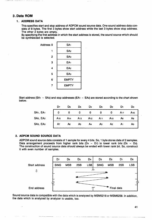
3.Data ROM 1. ADDRESS DATA
This specifies start and stop address of AOPCM sound source data. One sound address data consists of 8 bytes. The first 3 bytes show start address while the last 3 bytes show stop address. The other 2 bytes are empty. By specifying the first address in which the start address is stored, the sound source which should be synthesized is selected.
Address 0
2
3
4
5
6
7
SA1
SA2
SA3
EA1
EA2
EA3
EMPTY
EMPTY
Start address (SA1 - SA3) and stop addresses (EA1 - EA3) are stored according to the chart shown below.
SA1, EA1
SA2, EA2
SA3, EA3
0
A15
A7
2. ADPCM SOUND SOURCE DATA
Os
0
A14
As
05 04
0 0
A13 A12
A5 A4
03 02 01 Do
0 0 A17 A1S
An A10 As As
A3 A2 A1 Ao
AOPCM sound source data consists of 1 sample for every 4 bits. So, 1 byte stores data of 2 samples. Data arrangement proceeds from higher rank bits (04 - 07) to lower rank bits (Do - 03). The construction of sound source data should always be ended with lower rank bit. So, construct it with even number of samples.
07 Os 05 04 03 02 01 Do
Start address SING MSB 2SB LSB SING MSB 2SB LSB
.... - -
- -v "'
End address ====== -----y----. Final data i Sound source data is compatible with the data which is analyzed by MSM5218 or MSM6258. In addition, the data which is analyzed by analyzer is usable, too.
41
42
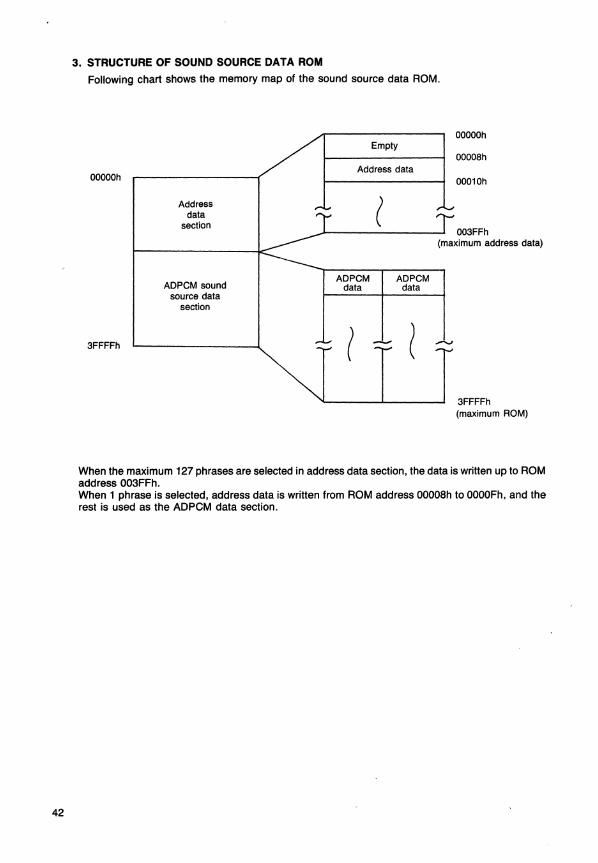
3. STRUCTURE OF SOUND SOURCE DATA ROM
Following chart shows the memory map of the sound source data ROM.
OOOOOh Empty
0OOO8h Address data
OOOOOh 0OO10h
Address ( data section 003FFh
(maximum address data)
ADPCM sound ADPCM ADPCM
data data source data
section
3FFFFh ( -- ( 3FFFFh (maximum ROM)
When the maximum 127 phrases are selected in address data section, the data is written up to ROM address 003FFh. When 1 phrase is selected, address data is written from ROM address 00008h to OOOOFh, and the rest is used as the ADPCM data section.
FUNCTIONAL DESCRIPTION
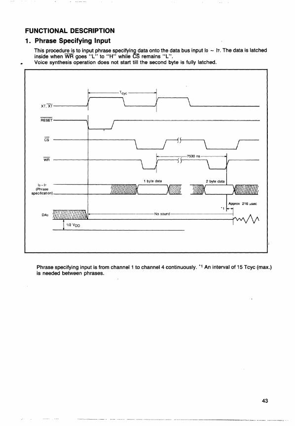
1. Phrase Specifying Input This procedure is to input phrase specifying data onto the data bus input 10 - 17. The data is latched inside when WR goes "L" to "H" while CS remains "L". Voice synthesis operation does not start till the second byte is fully latched.
XT,xr-{ RESET-----,I
cs
WR
10-17 (Phrase
speclflcatlon) _____ +-__ -'-lJ.J.J.1JI.J1JJ.u.w.1JJ '-___ --.J
\'--------
\,--_r-
DAo I-----------No sound----------l
Phrase specifying input is from channel 1 to channel 4 continuously. '1 An interval of 15 Tcyc (max.) is needed between phrases. .
43
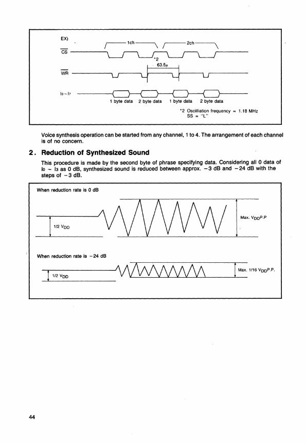
EX) r--1Ch~ ;---2ch~
CS -------, ,------
WR
10-17
1 byte data 2 byte data 1 byte data 2 byte data
• 2 Oscilliation frequency = 1.18 MHz SS = "L"
Voice synthesis operation can be started from any channel, 1 to 4. The arrangement of each channel is of no concern.
2. Reduction of Synthesized Sound
44
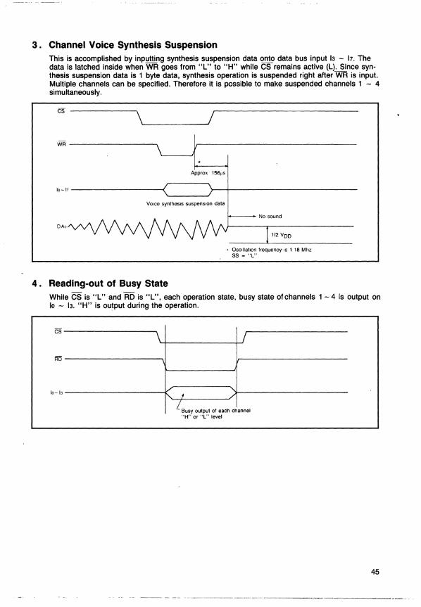
This procedure is made by the second byte of phrase specifying data. Considering a" 0 data of 10 - 13 as 0 dB, synthesized sound is reduced between approx. - 3 dB and - 24 dB with the steps of - 3 dB.
When reduction rate is 0 dB
------11/2vDD-v\/VVVW l·~ '00"
When reduction rate is - 24 dB
-'~1n-VD-D--------~~ I Max. 1116 VDDP,P,
3. Channel Voice Synthesis Suspension This is accomplished by inputting synthesis suspension data onto data bus input 13 - 17. The data is latched inside when WR goes from "L" to "H" while CS remains active (L). Since synthesis suspension data is 1 byte data, synthesis operation is suspended right after WR is input. Multiple channels can be specified. Therefore it is possible to make suspended channels 1 - 4 simultaneously.
C5 --------~\~ ______ ~/
WR -------------------,
Approx 156"5
10-17 ------------------<
VOIce syntheSIS suspension data
DAo
4. Reading-out of Busy State
• OSCillation frequency IS 1 18 Mhz 55 = "L"
While CS is "L" and RD is "L", each operation state, busy state of channels 1 - 4 is output on 10 - 13. "H" is output during the operation.
/
10-13 ./ " "- I ./
i Busy output of each channel "H" or "L" level
45
s. Output of Voice Synthesized -Sound
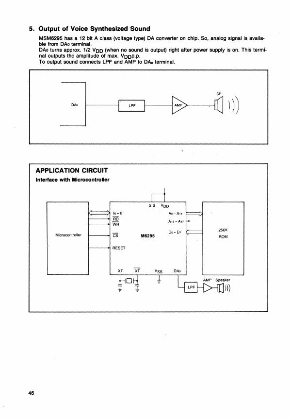
46
MSM6295 has a 12 bit A class (voltage type) OA converter on chip. So, analog signal is available from OAo terminal. OAo turns approx. 112 VOO (when no sound is output) right after power supply is on. This terminal outputs the amplitude of max. VOOP.p. To output sound connects LPF and AMP to OAo terminal.
OAo
APPLICATION CIRCUIT Interface with Mlcrocontroller
Microconlroller
10-17
Ri5 WR
CS
RESET
XT
SS VOO
Ao-A14
A'5-A17
00-07 M6295
XT OAo
256K
ROM
n)
OKI semiconductor
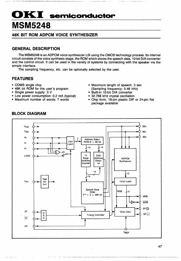
MSM5248 48K BIT ROM ADPCM VOICE SYNTHESIZER
GENERAL DESCRIPTION
The MSM5248 is an ADPCM voice synthesizer LSI using the CMOS technology process. Its internal circuit consists of the voice synthesis stage, the ROM which stores the speech data, 10-bit D/A converter and the control circuit. It can be used in the variety of systems by connecting with the speaker via the simple interface.
The sampling frequency, etc. can be optionally selected by the user.
FEATURES
• COMS single chip • 48K bit ROM for the user's program • Single power supply: 3 V • Low power consumption: 0.2 rnA (typical) • Maximum number of words: 7 words
BLOCK DIAGRAM
VDD
VSS
• Maximum length of speech: 3 sec (Sampling frequency: 5.46 kHz)
• Built-in 10-bit D/A converter • 32.768 kHz crystal oscillation • Chip form, 18-pin plastic DIP or 24-pin flat
package available
.---__ --1>--___ oJ SD,
~--_+__--.. Jo SD1
Ao I ~ r Address Select I 0-_---+1-__..---1 3·bIt r-r-l ROM 8 x 28 bit
~.: .--t.:=t SDo
A2
LOAD 14 END Stage Address
/" ADPCM
Address Detec- SyntheSizer Counter tor
1--.-
~ 12 14
H 12-bIt Latch Test
Test ()....... CIr· 1---+ CUlt
Speech Data MSB 9 ROM
214 x 3 ~ 48K bit - MSB
~ MSB
XT
XT
t ~1 C SPG)
10·blt DAC spG
1 Tlmtng C.Jntrolier
AC
47
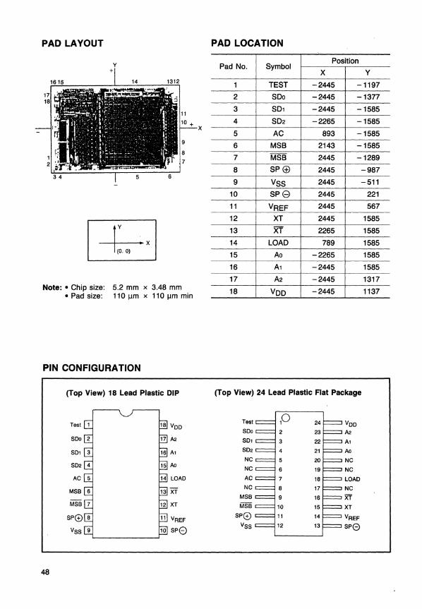
PAD LAYOUT PAD LOCATION
Pad No. Symbol Position
X y
1 TEST -2445 -1197
2 SDo -2445 -1377
3 SD1 -2445 -1585
4 SD2 -2265 -1585 x
5 AC 893 -1585
6 MSB 2143 -1585
7 MSB 2445 -1289
8 SP <±> 2445 -987
9 VSS 2445 -511
10 SP8 2445 221
11 VREF 2445 567
12 XT 2445 1585
13 XT 2265 1585
14 LOAD 789 1585
15 Ao -2265 1585
16 A1 -2445 1585
17 A2 -2445 1317 Note: • Chip size: 5.2 mm x 3.48 mm
• Pad size: 110 IJm x 110 IJm min 18 VDD -2445 1137
PIN CONFIGURATION
(Top View) 18 Lead Plastic DIP (Top View) 24 Lead Plastic Flat Package
Test VOO SOo A2 S01 A1 S02 Ao NC NC NC NC AC LOAD NC NC
MSB XT
MSB XT
11 VREF Spe VREF
SP8 VSS SpG
48
ELECTRICAL CHARACTERISTICS
Absolute Maximum Ratings Table 1 (VSS = 0 V)
Parameter Symbol Conditions Limit Unit
Supply Voltage VOO -0.3 to +3.6 V Ta = 25°C
Input Voltage VI -0.3 to VOO V
Power Oissipation Po 200 max mW
Storage Temperature Tstg - -55 to +150 °C
Operating Range Table 2
Parameter Symbol Conditions Limit Unit
Supply Voltage VOO - +2.4 to +3.6 V
Operating Temperature Top - -10 to +60 °C
External Reference Resistor RREF Applicable for VREF Min 100 kQ
DC Characteristics Table 3 (VOO = 3.1 V, VSS = 0 V, Ta = 25°C)
Parameter Symbol Conditions Min Typ Max
"H" Input Voltage VIH - 2.5 - -"L" Input Voltage VIL - - - 0.5
, "H" Input Voltage *1 IIH VIH = 3.1 V - - 1
"L" Input Voltage IlL VIL = 0 V - - -1
"H" Input Voltage *2 IIH1 VIH1 = 3.1 V 7 - 200
"H" Output Voltage *3 IOH VOH = 2.5 V -0.1 - -"L" Output Voltage *3 IOL VOL = 0.5.V 0.1 - -Power Consumption (1) 1001 Active - 0.2 1.0
Power Consumption (2) 1002 Standby (no oscillation) - - 1
Power Consumption (3) 1003 Standby (oscillation) - 10 20
OA Synk Current *4 ISYNK Note 1 260 400 600
OA Accuracy *4 IE Note 2 0.75 1 1.25 x1 x 1
Notes: *1 Applicable for Ao, A1, A2, when pull down resistor is not provided. * 2 Applicable for LOAO, AC and Ao, A1 and A2 when pull down resistor is applied. * 3 Applicable for MSB, MSB. * 4 Applicable for SP <±> ' SP e .
Unit
V
V
IlA
IlA IlA
mA
mA
mA
IlA
IlA
IlA
IlA
49
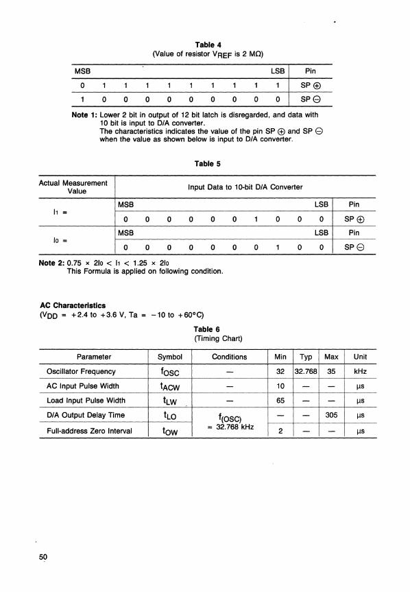
Table 4 (Value of resistor VREF is 2 MQ)
MSB LSB Pin
o SP@
o o o o o o o o o SP8
Note 1: Lower 2 bit in output of 12 bit latch is disregarded, and data with 10 bit is input to D/A converter. The characteristics indicates the value of the pin SP @ and SP 8 when the value as shown below is input to D/A converter.
Table 5
Actual Measurement Input Data to 1Q-bit D/A Converter Value
MSB LSB h =
0 0 0 0 0 0
MSB 10 =
0 0 0 0 0 0
Note 2: 0.75 x 210 < h < 1.25 x 210 This Formula is applied on following condition.
AC Characteristics (VDD = +2.4 to +3.6 V, 1a = -10to +600 C)
Parameter
Oscillator Frequency
AC Input Pulse Width
Load Input Pulse Width
D/A Output Delay Time
Full-address Zero Interval
50
Symbol
fosc
tACW
tLW
tLO
tow
Table 6 (Timing Chart)
Conditions
---
f(OSC) = 32.768 kHz
1 0 0 0
LSB
0 1 0 0
Min Typ Max
32 32.768 35
10 - -65 - -- - 305
2 - -
Pin
SP@
Pin
SP8
Unit
kHz
IlS
IlS
Ils
IlS
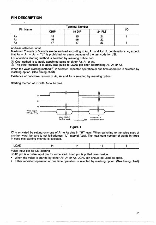
PIN DESCRIPTION
Terminal Number Pin Name
CHIP 18 DIP 24 FLT 1/0
Ao 15 15 21 I Al 16 16 22 A2 17 17 23 I
Address selection input Maximum 7 words or 3 words are determined according to Ao, Al, and A2 H/L combinations -, except that Ao = Al = A2 = "L" is prohibited for users because of the test code for LSI. LSI operation starting method is selected by masking option, too. CD One method is to-apply appointed pulse- to either-Ao, Al or A2. ® The other method is to apply 10ad pulse to LOAD pin after determining Ao, Al or A2.
When the voice starting method CD is selected, repeated operation or one time operation is selected by masking option. (See timing chart)
Existence of pull-down resistor of Ao, Al and A2 is selected by masking option.
Starting method of IC with Ao to A2 pins.
Ao
Al --------II----'-~
A2----------~I----~~---~I------
VOice output (SPIj). SPG)
VOice start of the first word
VOice start of _-i-~t""ow the second word
Figure 1
IC is activated by setting only one of Al to A2 pins in "H" level. When switching to the voice start of another word, be sure to set full-address "L" interval (tow). The maximum number of words in three in case this starting method is selected.
LOAD 14 14 18
Pulse input pin for LSI starting LOAD pin is a pulse input pin for voice start. Load pin is pulled down inside. • When the voice is started by either Ao, Al or A2, LOAD pin should be used as open. • Either repeated operation or one time operation is selected by masking option. (See timing chart)
51
PIN DESCRIPTION (Continued)
Terminal Number Pin Name
CHIP 18 DIP 24 FLT
XT 12 12 15 XT 13 13 16
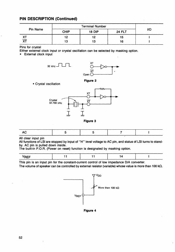
Pins for crystal Either external clock input or crystal oscillation can be selected by masking option. • External clock input
32kHZJL.JL XT
Q-C>o J. ~ Open 0-Figure 2
• Crystal oscillation
Crystal ~,.-------<~ n ~ """H, !lD~ ~~-----'
Figure 3
AC 5 5 7
All clear input pin
110
I I
All functions of LSI are stopped by input of "H" level voltage to AC pin, and status of LSI turns to standby. AC pin is pulled down inside. The built-in P.O.A. (Power on reset) function is deSignated by masking option.
11 11 14
This pin is an input pin for the constant-current control of low impedance D/A converter. The volume of speaker can be controlled by external resistor (variable) whose value is more than 100 kO.
More than 100 kO
Figure 4
52
PIN DESCRIPTION (Continued)
Terminal Number Pin Name
CHIP 18 DIP 24 FLT 1/0
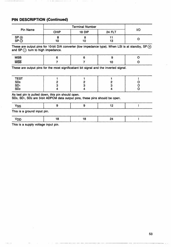
SP~ 8 8 11 0 SP8 10 10 13
These are output pins for 10-bit OIA converter (low impedance type). When LSI is at standby, SP e±:> and SP e turn to high impedance.
MSB
MSB
6
7
6
7
9
10
These are output pins for the most significatiant bit signal and the inverted signal.
TEST SOo S01 S02
1 2 3 4
As test pin is pulled down, this pin should open.
1 2 3 4
1 2 3 4
SOo, S01, S02 are 3-bit AOPCM data output pins, these pins should be open.
VSS 9 9 12
This is a ground input pin.
VOO 18 18 24
This is a supply voltage input pin.
o o
I o o o
53
TIMING CHART
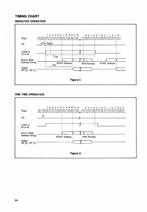
REPEATED OPERATION
fosC
AC
LOAD or Ao to A2
Built-in ROM Address Timing
Output ([email protected])
2 3 4 5 6 7 8 9101112 abc d e f g h I j k j m
~r--r------r~---+--~I~~----~ __________ ~ __ I.
I I END Address
I START Address I
:----~----------I I
'''--~~--~t.==
Figure 5
ONE TIME OPERATION
54
fosc
AC
LOAD or Ao to A2
6 7 8 9 1011 12 abcdefghljklmno
~L-----~----4-~Hf------~------------I
! II I I
-------~:~, ~--------------BUiltlnROM _ ~~
Address Timing START Address: END Address
Output _____________________ ir--ilr----1J---__________________ _ ([email protected]) L--(f
Figure 6
TYPICAL APPLICATION CIRCUIT
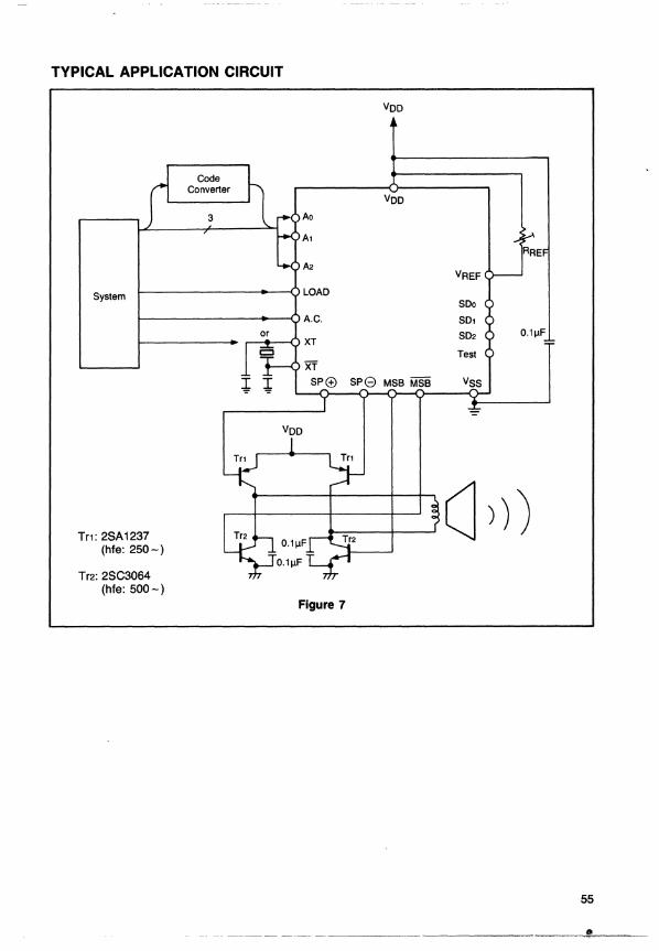
System
Tr1: 2SA 1237 (hfe: 250-)
Tr2: 2SC3064 (hfe: 500-)
VOO
Figure 7
VOO
VOO
SP8 MSB MSB
RE
VREF
SOo
SOl
S02 O.1~F
Test
VSS
-=-
55
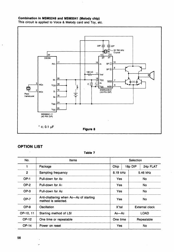
Combination in MSM5248 and MSM5041 (Melody chip) This circuit is applied to Voice & Melody card and Toy, etc.
22P
22
OSCIN
16 R01~1~7 _____ +-4-__ ~ A1
32768 kHz Crystal
spG 10
spEB 8
Pezo transducer
M1 39
MO, VDD 38
MO,
MSM5041-11 (40 PIN DIP)
S1 19
• c; 0.1 IlF
100 kO
-
Figure 8
OPTION LIST
Table 7
No. Items
1 Package
2 Sampling frequency
OP·1 Pull-down for Ao
OP-2 Pull-down for Al
OP-3 Pull-down for A2
OP-7 Anti-chattering when Ao-A2 of starting method is selected.
OP-9 Oscillation
OP-10, 11 Starting method of LSI
OP-12 One time or repeatable
OP-14 Power on reset
56
11 Vref C] A, Ms8
VSS MSB
MSM5248-01 (18 PIN DIP)
Selection
Chip I 18p DIP I 24p FLAT
8.19 kHz 5.46 kHz
Yes No
Yes No
Yes No
Yes No
X'tal External clock
Ao-A2 LOAD
One time Repeatable
Yes No
~ 9 (OP-12)
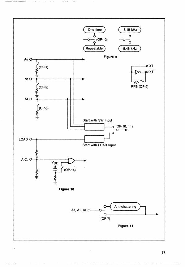
( Repeatable)
Ao G T Figure 9
( 8.19 kHZ)
2) -0-« ( 5.46 kHZ)
t(OP-l l
A1 1
i(OP-2) 6 XT
XT
A2 T
f(OP-31
Start with SW Input
RFB (OP-9)
(OP-10,11) ---0---.
LOAOGo-~----------------~1 L..-__ --'
Start with LOAD Input
~ A.C.o-~T---:-;---j)-
VOO I -" t (OP-l.j
Figure 10
:c Anti-chattering 2J Ao, A1, A2 o-----<:r-
--------------~~--.~ (OP-7)
Figure 11
57
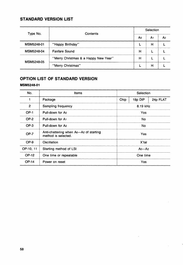
STANDARD VERSION LIST
Type No. Contents
MSM5248-01 "Happy Birthday"
MSM5248-04 Fanfare Sound
"Merry Christmas & a Happy New Year" MSM5248-05
"Merry Christmas"
OPTION LIST OF STANDARD VERSION
MSM5248·01
No. Items
1 Package
2 Sampling frequency
OP-1 Pull-down for Ao
OP-2 Pull-down for A1
OP-3 Pull-down for A2
OP-? Anti-chattering when Ao-A2 of starting method is selected.
OP-9 Oscillation
OP-10, 11 Starting method of LSI
OP-12 One time or repeatable
OP-14 Power on reset
58
Selection
Ao A1 A2
L H L
H L L
H L L ---
L H L
Selection
Chip I 18p DIP I 24p FLAT
8.19 kHz
Yes
No
No
Yes
X'tal
Ao-A2
One time
Yes
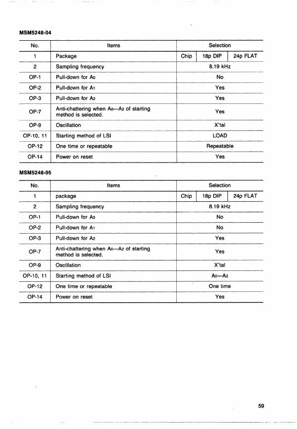
MSM5248-04
No. Items Selection
1 Package Chip I 18p DIP I 24p FLAT
2 Sampling frequency 8.19 kHz
OP-1 Pull-down for Ao No
OP-2 PUll-down for A1 Yes
OP-3 Pull-down for A2 Yes
OP-7 Anti-chattering when Ao-A2 of starting Yes method is selected.
OP-9 Oscillation X'tal
OP-10, 11 Starting method of LSI LOAD
OP-12 One time or repeatable Repeatable
OP-14 Power on reset Yes
MSM5248-05
No. Items Selection
1 package Chip I 18p DIP I 24p FLAT
2 Sampling frequency 8.19 kHz
OP-1 Pull-down for Ao No
OP-2 Pull-down for A1 No
OP-3 Pull-down for A2 Yes
OP-7 Anti-chattering when Ao-A2 of starting Yes method is selected.
OP-9 Oscillation X'tal
OP-10, 11 Starting method of LSI Ao-A2
OP-12 One time or repeatable One time
OP-14 Power on reset Yes
59
OKI semiconductor
MSM6243 SPEECH SYNTHESIS LSI WITH 192 KBIT ROM
GENERAL DESCRIPTION
The Oki MSM6243 is a single-chip, CMOS, speech synthesis LSI for AOPCM systems. It contains 192k bits of speech data ROM storage. This IC has an input interface, a timing generation circuit, and a 10 bit OA converter. Therefore, voice output systems may be constructed easily by connecting the voice output circuit consisting of a simple input circuit, filter, amplifier, and speaker to the chip.
FEATURES
• CMOS single chip • Low power consumption • Custom ROM • Selection of supply voltage: 3V system or 5V
system. • AOPCM bit length: 4 bits • Maximum word number: 124 words • Maximum speaking time: 20 seconds
(compressed AOPCM) • Selection of class A or class B analogue
output is possible. • Built-in 10 bit OA converter
BLOCK DIAGRAM
VOD
VDO'
Vss
LOAD
BUSY/NAR
XT Xl'
AC
tr >------
r-
-- ~1 15 ...
T I c>--
~
Address Select ROM
124x14 bit
t'4
14 bit Address Counter
t'4
192 kblt DATA ROM
(214X12 bit)
i Control CIrCUIt
11
T" T2, SIP and S03, SD2 , SO" SOo are test pins.
60
• Oscillator frequency: 30 to 132 kHz (5V system).
• Chip, 40 pins plastic DIP, 44 pins or 60 pins plastic flat package. 2 types of plastic flat package are provided depending on terminal pin bending or not bending.
Terminal pin not bending MSM6243-XXGS
Terminal pin bending MSM6243-XXGS-K
When placing an order, specify the type. • Word selection through an internal random
number circuit is possible (maximum 32 words).
,.
,---
I --~
~=§ -
~:. -
12 -
I
1
J ADPCM Synthe·
sizer
t'2
12 btt Latch
110
10 bit DAC
SLA SLB
~
---<~ ---<~
SD, SD, SO,
SDo
SIP
MSB
DAU
DAL
SPE VCK
PAD LAYOUT PAD LOCATION
Pad No. Symbol Position
X Y
1 SLB -2300 -1125
2 VDD' -2300 -1425
3 SLA -2300 -1725
4 MSB -2300 -2000
5 DAU -2300 -2570
6 DAL -2110 -2615
7 SPE -1560 -2615
8 VCK -675 -2625
9 SIP -395 -2625
10 VSS 885 -2625
11 SDo 1075 -2625
12 SD1 1480 -2625
13 SD2 1660 -2625
14 SD3 2060 -2625 y
15 T2 2295 -2325
x 16 T1 2295 -1925
(0.0) 17 LOAD 2295 -1745
18 Ao 2295 -1345
19 A1 2295 440
20 A2 2295 745
21 A3 2295 1145 Note: • Chip size: 4.91 mm x 5.57 mm
• Chip thickness: 350 ± 30 11m 22 A4 2295 1325
23 As 2295 1730
24 As 2295 1910
25 AC 2295 2310
26 BUSY/NAR 2295 2625
27 VDD 1965 2625
28 XT 1650 2625
29 XT 1345 2625
61
PIN CONFIGURATION
(Top View) 40 Lead Plastic DIP
Vss
A.
As
As
AC
BUSY/NAR
Voo
Xi
XT
SIP
VCK
SPE
DAL
DAU
MSB
SLA
VOOI
SLB
NC
NC
NC
NC
NC
NC
NC
NC
NC
NC
NC
Note: This pinout applies to the MSM6243-XXRS.
62
(Top View) 44 Lead Plastic Flat Package
T2 MSB
0 SLA
VDD
SLB
A, NC
NC
NC
A4 NC
NC
A,; NC
AC NC
cr: Q
I!K !K u Q 0 0 0 0 0 « Q z Z z z z z > Q Z > ): (f) ::::J co
Note 1. This pinout applies to the MSM6243-XXGS and -XXGS-K. Note 2. Since 17 and 39 pin (Voon) is substrate continuity, short-circuits with Voo and Voo'
in the outside.
63
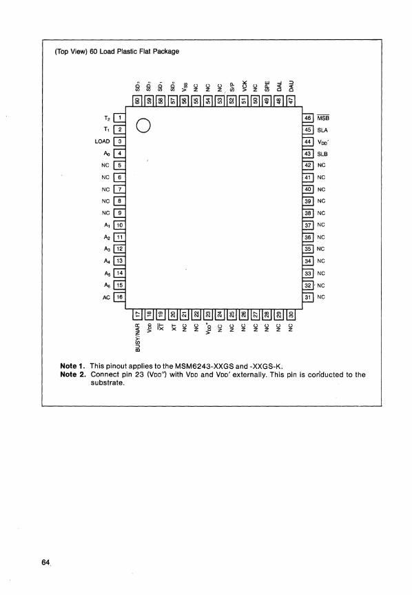
(Top View) 60 Load Plastic Flat Package
0 0 0 0 '" Q. lc: W ...J :;)
'" () () () en () () Q. C'i C'i en en en en > z z z > z en
T2
0 MSB
T, SLA
Voo'
SLB
NC NC
NC
NC
NC
NC
A, NC
A2 NC
~ NC
Ai NC
As NC
~
AC
a:: 0 I~ ~ () () .
() () () () () () () 0 0 « > z z ~ z z z z z z z z
:;: en :;)
III
Note 1. This pinout applies to the MSM6243-XXGS and -XXGS-K. Note 2. Connect pin 23 (Voo") with Voo and Voo' externally. This pin is con'ducted to the
substrate.
ELECTRICAL CHARACTERISTICS
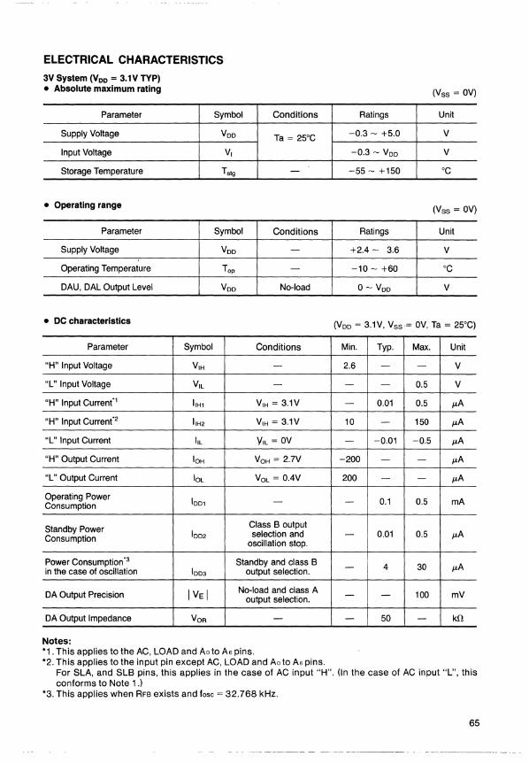
3V System (Voo = 3.1 V TYP) • Absolute maximum rating
Parameter
Supply Voltage
Input Voltage
Storage Temperature
• Operating range
Parameter
Supply Voltage
Operating Temperature
DAU, DAL Output Level
• DC characteristics
Parameter
"H" Input Voltage
"L" Input Voltage
"H" Input Current"1
"H" Input Current"2
"L" Input Current
"H" Output Current
"L" Output Current
Operating Power Consumption
Standby Power Consumption
Power Consumption'3
in the case of oscillation
DA Output Precision
DA Output Impedance
Notes:
Symbol
VIH
VIL
IIHI
IIH2
IlL
IOH
IOL
1001
1002
1003
I VE I
VOR
Symbol Conditions
Voo Ta = 25DC
VI
T5tg -
Symbol Conditions
Voo -Top -
Voo No-load
Conditions
--
VIH = 3.1V
VIH = 3.1V
VIL = OV
VOH = 2.7V
VOL = O.4V
-
Class B output selection and
oscillation stop.
Standby and class B output selection.
No-load and class A output selection.
-
*1. This applies to the AC, LOAD and Ao to As pins. *2. This applies to the input pin except AC, LOAD and Ao to As pins.
(Vss = OV)
Ratings Unit
-0.3 - +5.0 V
-0.3 - Voo V
-55 - +150 DC
(Vss = OV)
Ratings Unit
+2.4 - 3.6 V
-10 - +60 DC
0- Voo V
(Voo = 3.1V, Vss= OV, Ta = 25DC)
Min. Typ. Max. Unit
2.6 - - V
- - 0.5 V
- 0.01 0.5 p..A
10 - 150 p..A
- -0.01 -0.5 p..A
-200 - - p..A
200 - - p..A
- 0.1 0.5 mA
- 0.01 0.5 p..A
- 4 30 p..A
- - 100 mV
- 50 - kO
For SLA, and SLB pins, this applies in the case of AC input "H". (In the case of AC input "L", this conforms to Note 1 .)
*3. This applies when RFB exists and fose = 32.768 kHz.
65
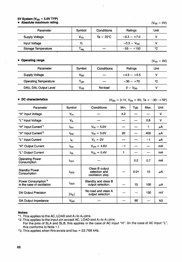
SV System (Voo = S.OV TYP) • Absolute maximum rating
Parameter
Supply Voltage
Input Voltage
Storage Temperature
• Operating range
Parameter
Supply Voltage
Operating Temperature
DAU, DAL Output Level
Symbol
Voo
VI
T'19
Symbol
Voo
Top
Voo
(Vss = OV)
Conditions Ratings Unit
Ta = 25°C -0.3 ~ +7.0 V
-0.3 ~ Voo V
- -55 ~ +150 °C
(Vss = OV)
Conditions Ratings Unit
- +4.5 ~ +5.5 V
- -30 ~ +70 °C
No-load o ~ Voo V
• DC characteristics (Voo = 3.1V, Vss = OV, Ta = -30~+700)
Parameter Symbol Conditions Min. Typ. Max. Unit
"H" Input Voltage VIH - 4.2 - - V
"L" Input Voltage VIL - - - 0.8 V
"H" Input Current'l IIHI VIH = 5.0V - - 1 p.,A
"H" Input Current'2 IIH2 VIH = 5.0V 20 - 400 p.,A
"L" Input Current IlL VIL = OV - - -1 p.,A
"H" Output Current 10H VOH = 4.SV -1 - - mA
"L" Output Current IOL VOL = O.4V 1 - - mA
Operating Power Consumption IDOl - 0.2 0.7 mA
Standby Power Class B output
1002 selection and - 0.01 10 p.,A Consumption oscillation stop.
Power Consumption'3 10D3
Standby and class B in the case of oscillation output selection. - 15 100 p.,A
DA Output Precision No-load and class A - - 130 mV IVel output selection
DA Output Impedance VOR - - so - kO
Notes: *1. This applies to the AC, LOAD and Ao to A6 pins. *2. This applies to the input pin except AC, LOAD and Ao to A6 pins.
For the pins of SLA and SLB, this applies in the case of AC input "H". (In the case of AC input "L", this conforms to Note 1 .)
*3. This applies when RFB exists and fose = 32.768 kHz.
66
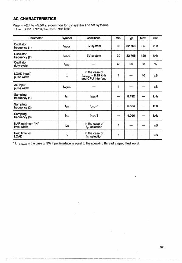
AC CHARACTERISTICS
(Voo = +2.4 to +5.5V are common for 3V system and 5V systems. Ta = -30 to +70°C, fose = 32.768 kHz.)
Parameter Symbol Conditions
Oscillator fosc1 3V system frequency (1)
Oscillator fosc2 5V system frequency (2)
Oscillator fduty -duty-cycle
LOADinpu(1 In the case of tL fsample = 8.19 kHz pulse width and CPU interface
AC input pulse width tW(AC) -
Sampling fS1 fosc/4 frequency (1)
Sampling f52 fosc/5 frequency (2)
Sampling fS3 fosc/8 frequency (3)
NAR minimum "H" tMN
I n the case of level width fS1 selection
Hold time for tH
In the case of LOAD fS1 selection
Min. Typ.
30 32.768
30 32.768
40 50
1 -
1 -
- 8.192
- 6.554
- 4.096
1 -
1 -
*1. tL(MAX) in the case qf SW input interface is equal to the speaking time of a specified word.
Max. Unit
35 kHz
120 kHz
60 %
40 ILS
- ILS
- kHz
- kHz
- kHz
- ILS
- ILS
67
PIN DESCRIPTION
Terminal Number Pin Name
CHIP 40 DIP 44 FLT 60 FLT 1/0
AC 25 16 11 16 I
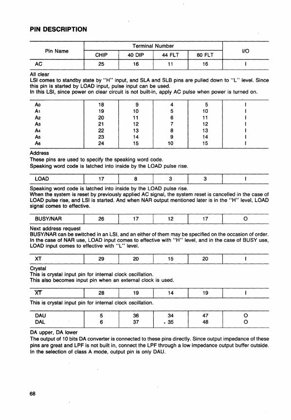
All clear LSI comes to standby state by "H" input, and SLA and SLB pins are pulled down to "L" level. Since this pin is started by LOAD input, pulse input can be used. In this LSI, since power on clear circuit is not built-in, apply AC pulse when power is turned on.
Ao 18 9 4 5 I Al 19 10 5 10 I A2 20 11 6 11 I A3 21 12 7 12 I A4 22 13 8 13 I As 23 14 9 14 I As 24 15 10 15 I
Address These pins are used to specify the speaking word code. Speaking word code is latched into inside by the LOAD pulse rise.
LOAD 17 8 3 3
Speaking word code is latched into inside by the LOAD pulse rise. When the system is reset by previously applied AC signal, the system reset is cancelled in the case of LOAD pulse rise, and LSI is started. And when NAR output mentioned later is in the "H" level, LOAD signal comes to effective.
BUSY/NAR 26 17 12 17 o Next address request BUSY/NAR can be switched in an LSI, and an either of them may be specified on the occasion of order. In the case of NAR use, LOAD input comes to effective with "H" level, and in the case of BUSY use, LOAD input comes to effective with "L" level.
XT 29 20 15 20
Crystal This is crystal input pin for internal clock oscillation. This also becomes input pin when an external clock is used.
Xi 28 19 14 19
This is crystal input pin for internal clock oscillation.
DAU 5 36 34 47 0 DAL 6 37 • 35 48 0
DA upper, DA lower The output of 10 bits DA converter is connected to these pins directly. Since output impedance of these pins are great and LPF is not built in, connect the LPF through a low impedance output buffer outside. In the selection of class A mode, output pin is only DAU.
68
PIN DESCRIPTION (Continued)
Terminal Number Pin Name
CHIP 40 DIP 44 FLT 60 FLT 1/0
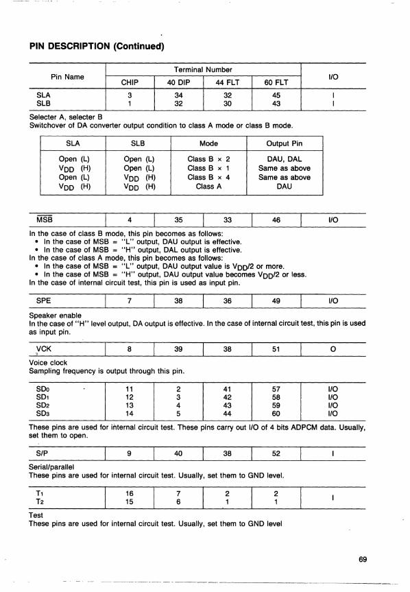
SLA 3 34 32 45 I SLB 1 32 30 43 I
Selecter A, selecter B Switchover of DA converter output condition to class A mode or class B mode.
SLA SLB Mode Output Pin
Open (L) Open (L) Class B x 2 DAU, DAL VDD (H) Open (L) Class B x 1 Same as above Open (L) VDD (H) Class B x 4 Same as above VOD (H) VOO (H) Class A DAU
MSB 4 35 33 46 1/0
In the case of class B mode, this pin becomes as follows: • In the case of MSB = "L" output, OAU output is effective. • In the case of MSB = "H" output, DAL output is effective.
In the case of class A mode, this pin becomes as follows: • In the case of MSB = "L" output, DAU output value is VDD/2 or more. • In the case of MSB = "H" output, DAU output value becomes VDD/2 or less.
In the case of internal circuit test, this pin is used as input pin.
SPE 7 38 36 49 1/0
Speaker enable In the case of "H" level output, DA output is effective. In the case of internal circuit test, this pin is used as input pin.
VCK 8 39 38 51 o • Voice clock Sampling frequency is output through this pin.
SDo 11 2 41 57 I/O SDl 12 3 42 58 1/0 SD2 13 4 43 59 1/0 SD3 14 5 44 60 1/0
These pins are used for internal circuit test. These pins carry out 1/0 of 4 bits ADPCM data. Usually, set them to open.
SIP 9 40 38 52
Serial/parallel These pins are used for internal circuit test. Usually, set them to GNO level.
Tl T2
Test
16 15
7 6
2 1
2 1
These pins are used for internal circuit test. Usually, set them to GND level
69
TIMING CHART Power On
Voo
AC
NAR r--:-ff _____ J '
LSI Start and No Operation (Standby) 1. Start In the case of CPU interface
LOAD
NAR
BUSY
SPE
DAUor DAL output
__ ~I~ ~} --!IH~
____ ~---JI tL --! tMN ~/r/-----------Approx. r---l ,..-----------I=--:: 1.1 msec -----=j I Irl
----~I ~1~ __________ _ Approx.
-1.0msec-/
r-----i~~:r-----~ ____ ---t-__ ~Sta~ndb~Y ::::J--1
, ~. ~===I Silent -Approx. ---I Approx. ----
1.5 msec 0.4 msec
First word speaking
(for 3 samples)
Second word speaking
2. Transfer to standby in the case of CPU interface
70
LOAD
NAR
BUSY
SPE
DAUor DAL output
_____ ~A~ __ E_N_D_co_de _____________ __
___________ ~rl~ _______________ __
--------- Last word--------... • t;1 =::::.:...:S~ta~n~d~by speaking "-
Speaking completed
When END code (Ao to As = "L") is accompanied with LOAD, LSI comes to the same state as standby because of AC input.
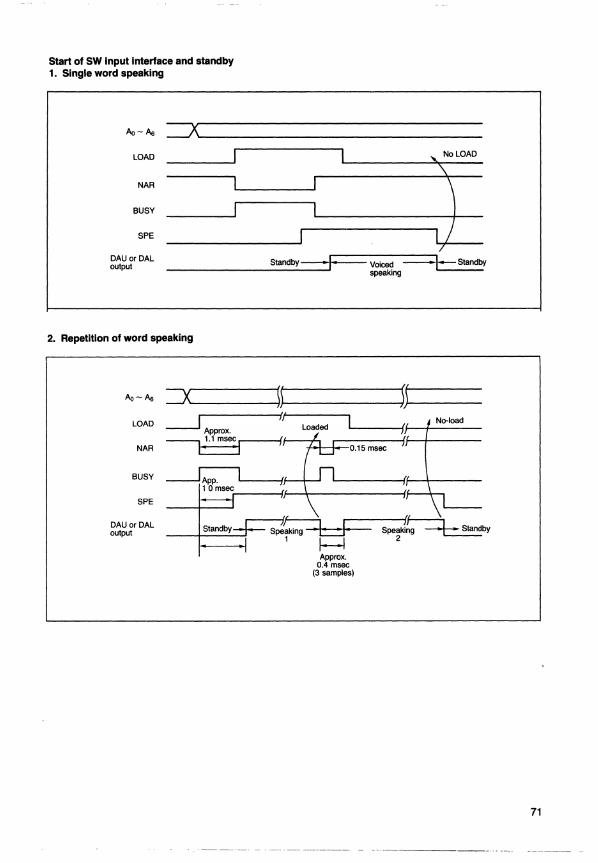
Start of SW input interface and standby 1. Single word speaking
Aa-~ ==x LOAD
NAR
BUSY
SPE
DAU or DAL output
2. Repetition of word speaking
Aa-~ =x LOAD -.-J Approx.
I
I
I
NAR ~ 1.lmsec. • -j
BUSY
SPE
DAU or DAL Standby output
I
I
I
Standby .,.
I~ " 1/
spe~' 1 I--l
Approx. 0.4 msec
(3 samples)
'" NoLOAD
\
1/ /
Voiced -b Standby speaking
~ /
~ ) Speaking Standby
2
71
FUNCTIONAL DESCRIPTION
Speaking Word Code Specification User can specify word codes set by Ao - Pte and can select either CPU interface or SW input interface.
1. CPU Interface In this case, user specified words are maximum 124 words. For Ao to As, the following 3 codes, "1111111", "0111111", "1011111", are test codes, and the code "0000000" is an END code, therefore, these 4 codes can not be used.
The procedure up to the LSI operation start is as follows: Input Ao to As - LOAD pulse apply - latched inside, also LSI operation starts simultaneously.
LOAD pulse is effective when NAR output is "H".
2. SW input interface By the reason described in clause 9.1.1. CPU interface, number of words is set to maximum 124 words with combination of Ao to Pte.
After the code is set by Ao to As, when "H" level LOAD input is switched by push switch, etc., the specified word starts speaking. (From standby to operation state).
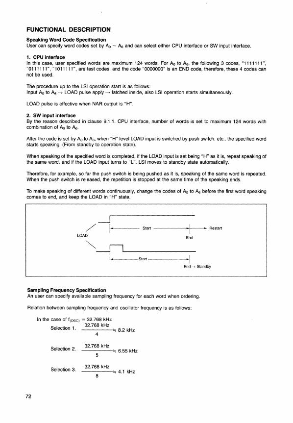
When speaking of the specified word is completed, if the LOAD input is set being "H" as it is, repeat speaking of the same word, and if the LOAD input turns to "L", LSI moves to standby state automatically.
Therefore, for example, so far the push switch is being pushed as it is, speaking of the same word is repeated. When the push switch is released, the repetition is stopped at the same time of the speaking ends.
To make speaking of different words continuously, change the codes of Ao to As before the first word speaking comes to end, and keep the LOAD in "H" state.
-.J
End
/ 1---LOAD
Start ------.41---· Restart
~~~---------1""1 ~---Start-------l'1
End .... Standby
Sampling Frequency Specification An user can specify available sampling frequency for each word when ordering.
Relation between sampling frequency and oscillator frequency is as follows:
In the case of f(osc) = 32.768 kHz
Selection 1. 32.768 kHz ·.8.2 kHz
4
Selection 2. 32.768 kHz
·.6.55 kHz 5
Selection 3. 32.768 kHz
·.4.1 kHz 8
72
Straight ADPCM and Compressed ADPCM 1. Straight ADPCM Features of the straight ADPCM are as follows: 1) ADPCM bit length ..... ~ .. Fixed in 4 bits. 2) Deletion of silent component is possible. 3) High bit rate, high tone quality. 4) Suitable for a sound effect
Bit rate (B'A) example:
UAMPLE = 8.2 kHz ADPCM bit length = 4 bits Deleted silent data'=; 1/5 (voice)
B·A '=; 8.2x4x4/5 '=; 26.3 kbits/sec
2. Compressed ADPCM Features of the compressed ADPCM are as follows: 1) ADPCM bit length ........ Fixed in 4 bits 2) Deletion of data by repeated detection of speech waveform. 3) Deletion of silent component is possible. 4) Low bit rate 5) Mainly applies to speech.
Bit rate example: fSAMPLE = 8.2 kHz
{ADPCM bit length = 4 bits Number of average waveform repetition = 3 (deleted data = 2/3) Deleted silent data,=; 1/5
B·A '=; 8.2x4x1/3x4/5 '=; 8.8 kbits/sec
Sampling Frequency and Band 1. Simple relation between sampling frequency and band fSAMPLEX1/2 = fBANo(uL)
Here, fBANo(uL) means upper limit of the band.
fSAMPLE fBAND Characteristics
8.2 kHz DC - 4.1 kHz Clear comprehending almost all tones of voice.
6.55 kHz DC - 3.2 kHz High tone female voice sounds usual.
4.1 kHz DC - 2.0 kHz Both male and female voices sound nasal and unclear.
2. Relation between sampling frequency and LPF (Low Pass Filter) is as follows: fSAMPLEX1/2 = fc (cut-off frequency of ideal filter)
Practically, according to the skirt characteristics of filter, fc shall be designed to be lower than the above mentioned equation. That is, the band will be further narrowed according to filter characteristics.
As an example, the fc and skirt characteristics of filter used for speech analysis by OKI are shown as follows.
fSAMPLE fc Skirt character fBAND
8.2 kHz 3.4 kHz -48 dB/oct Dc - 3.4 kHz
5.55 kHz 2.7 kHz -48 dB/oct DC - 2.7 kHz
4.1 kHz 1.7 kHz -48 dB/oct DC -1.7 kHz
73
J
., .... -.-.--.. ~--... ~-~~~---.-----... -.- .. ,-- , ..... _ ...
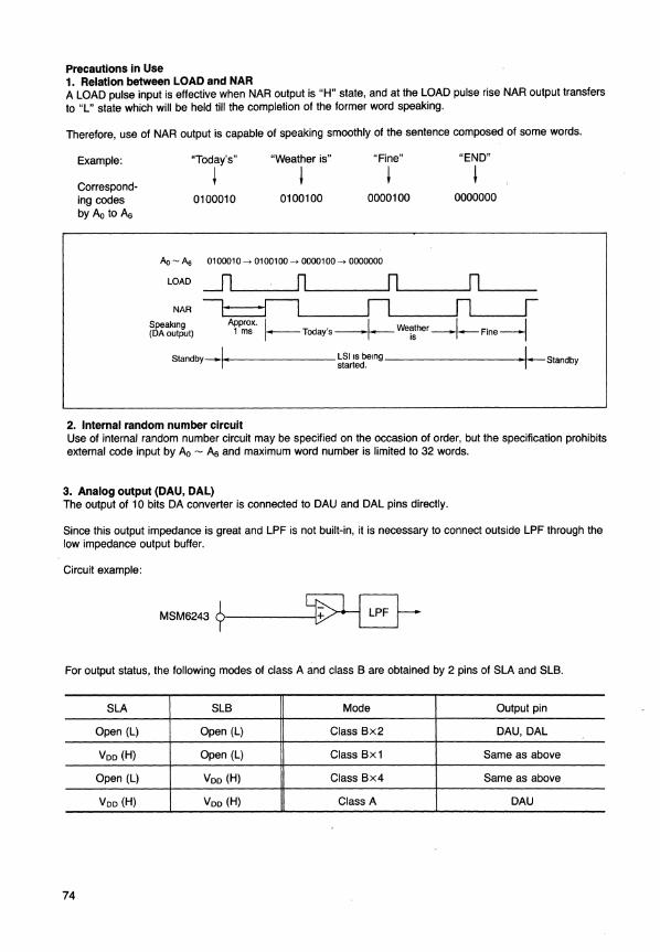
Precautions in Use 1. Relation between LOAD and NAR A LOAD pulse input is effective when NAR output is "H" state, and at the LOAD pulse rise NAR output transfers to "L" state which will be held till the completion of the former word speaking.
Therefore, use of NAR output is capable of speaking smoothly of the sentence composed of some words.
Example:
Correspond-ing codes by Ao to A6
"Today's" "Weather is" "Fine"
+ + + 0100010 0100100 0000100
Ao - A6 0100010 -> 0100100 -> 0000100 -> 0000000
LOAD
NAR Speaking (DAoutput)
"END"
+ 0000000
Standby_.+I .... -------LSI IS bemg----------.II-o.>--standbY started.
2. Internal random number circuit Use of internal random number circuit may be specified on the occasion of order, but the specification prohibits external code input by Ao - A6 and maximum word number is limited to 32 words.
3. Analog output (DAU, DAL) The output of 10 bits DA converter is connected to DAU and DAL pins directly.
Since this output impedance is great and LPF is not built-in, it is necessary to connect outside LPF through the low impedance output buffer.
Circuit example:
MSM6243 (}-------j
For output status, the following modes of class A and class B are obtained by 2 pins of SLA and SLB.
SLA SLB Mode Output pin
Open (L) Open (L) Class Bx2 DAU,DAL
Voo (H) Open (L) Class Bx1 Same as above
Open (L) Voo (H) Class Bx4 Same as above
Voo (H) Voo (H) Class A DAU
74
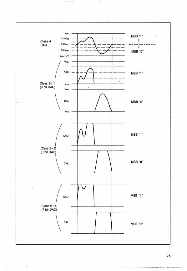
Voo
3/4Voo Class A DAU 1/2Voo
1/4Voo
voo=ov
( Voo
DAU
Class Bx1 vss (9 bit DAC)
voo
\ DAL
vss
(~ Class Bx2 (8 bit DAC)
\ '"
MSB "1"
t ----r------MSB "0"
MSB "1"
MSB "0"
MSB "1"
MSB "0"
MSB "1"
MSB "0"
75
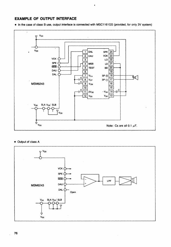
EXAMPLE OF OUTPUT INTERFACE • In the case of class B use, output interface is connected with MSC1161GS (provided, for only 3V system)
voo
Voo
VCK SPE
~ DAU
DAL
MSM6243
Vss SLA Voo' SLB
Vss
• Output of class A
Voo
MSM6243
VCK
SPE
MSB
DAU 0------1
DAL Open
Vss SLA voo' SLB
Vss
76
VCM
Note: Cs are all 0.1 /LF.
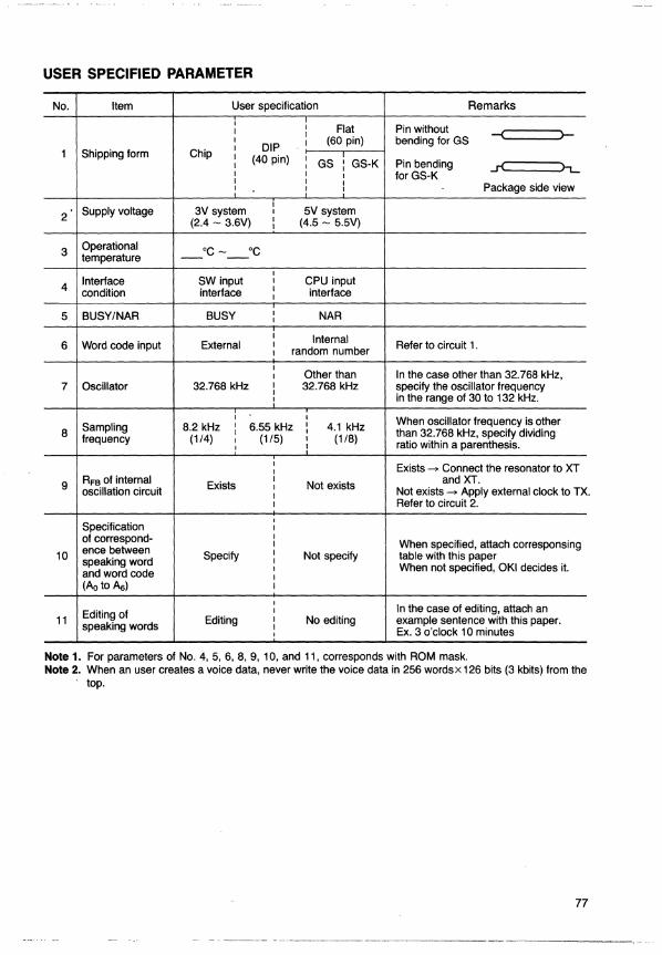
USER SPECIFIED PARAMETER
No. Item User specification Remarks
I I Flat Pin without I I -( >-I (60 pin) bending for GS I DIP I
1 Shipping form Chip I (40 pin) I I I GS I GS-K Pin bending Jf. >-t-I I I I for GS-K I I I Package side view I I I
Supply voltage 3V system I
5V system 2 I
(2.4 - 3.6V) I (4.5 - 5.5V) I
3 Operational °C _ °C temperature --I
4 Interface SW input I CPU input condition interface I interface I
5 BUSYINAR BUSY I NAR I
I Internal 6 Word code input External I Refer to circuit 1.
I random number I I Other than In the case other than 32.768 kHz,
7 Oscillator 32.768 kHz I 32.768 kHz specify the oscillator frequency I I in the range of 30 to 132 kHz.
I I When oscillator frequency is other Sampling 8.2 kHz I 6.55 kHz I 4.1 kHz 8 I I than 32.768 kHz, specify dividing frequency (1/4) (1/5) I (1/8) I
I ratio within a parenthesis. I
I Exists -> Connect the resonator to XT I
9 RFB of internal Exists I
Not exists and XT. oscillation circuit I Not exists -> Apply external clock to TX I
I Refer to circuit 2.
Specification , I
of correspond- I I When specified, attach corresponsing
10 ence between Specify I Not specify table with this paper speaking word I I When not specified, OKI decides it. and word code I
(Ao to A6) I
, In the case of editing, attach an
Editing of I
11 Editing I No editing example sentence with this paper. speaking words I I Ex. 3 o'clock 10 minutes
Note 1. For parameters of No.4, 5, 6, 8, 9, 10, and 11, corresponds with ROM mask. Note 2. When an user creates a voice data, never write the voice data in 256 words x 126 bits (3 kbits) from the
top.
77
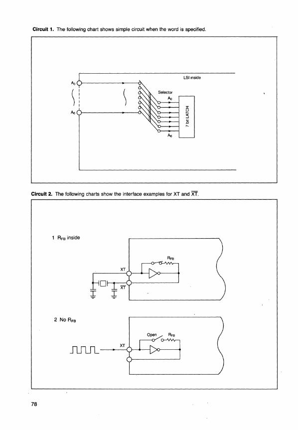
Circuit 1. The following chart shows simple circuit when the word is specified.
LSI Inside Ao
) J:
Ae u ~ .is ....
Ae
Circuit 2. The following charts show the interface examples for XT and XT.
1 RFB inside
78
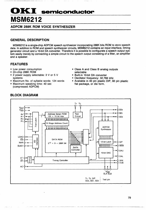
OKI semiconductor
MSM6212 ADPCM 288K ROM VOICE SYNTHESIZER
GENERAL DESCRIPTION
MSM6212 is a single-chip ADPCM speech synthesizer incorporating 288K bits ROM to store speech data. In addition to ROM and speech synthesizer circuits, MSM6212 contains an input interface, timing generator circuit and a 10-bit DA converter. Therefore it is possible to configurate a speech output system easily merely by connecting a simple circuit to the speech output consisting of a filter, an amplifier and a speaker.
FEATURES
• Low power consumption • On-chip 288K ROM • 2 power supply selectable: 3 V or 5 V
systems • Maximum No. of syllable words: 124 words • Maximum speaking time: 40 sec
(compressed ADPCM)
BLOCK DIAGRAM
VDD vss
Ao A, A2 A3
DATA ROM LOAD
cs NAR
BUSY 2'5 x 9 = 288K bit
XT XT Timing Controlier
• Class A and Class B analog outputs selectable
• Built-in 10-bit DA converter • Oscillator frequency: 32,768 kHz • Available in 40 pin plastic DIP, 60 pin plastic
flat package, or die form.
T, T2
SD2
SD,
SDo
SIP
:m:mtHEE~-? MSB
DAU
DAL
~==~--~~-+~--oSPE L-__ ~ ________________________ J--------t--i-~~VCK AC V---------'
VDD' SLA SLB
T" T2, SIP \ T t . SD2, SD" SDo es pin
79
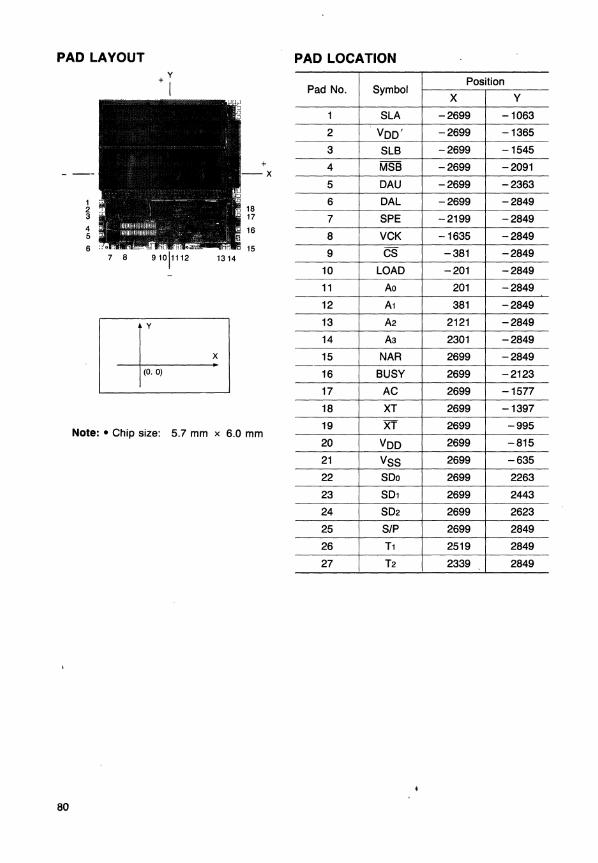
PAD LAYOUT
1 2 3
4 5
6
+y
I
Note: • Chip size: 5.7 mm x 6.0 mm
80
x
PAD LOCATION
Pad No. Symbol
1 SLA 2 VDD' 3 SLB 4 MSB 5 DAU 6 DAL 7 SPE 8 VCK 9 CS
10 LOAD 11 Ao 12 A1 13 A2 14 A3 15 NAR 16 BUSY 17 AC 18 XT 19 XT 20 VDD 21 VSS 22 SDo 23 SD1 24 SD2 25 SIP
26 T1 27 T2
Position X Y
-2699 -1063
-2699 -1365
-2699 -1545
-2699 -2091
-2699 -2363
-2699 -2849
-2199 -2849
-1635 -2849
-381 -2849
-201 -2849
201 -2849
381 -2849
2121 -2849
2301 -2849
2699 -2849
2699 -2123
2699 -1577
2699 -1397
2699 -995
2699 -815
2699 -635
2699 2263
2699 2443
2699 2623
2699 2849
2519 2849
2339 2849
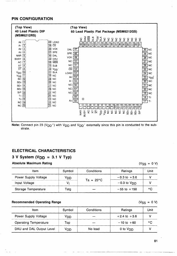
PIN CONFIGURATION
(Top View) (Top View) 40 Lead Plastic DIP 60 Lead Plasti.c Flat Package (MSM6212GS) (MSM6212RS)
~ 1m ~ ~8::s u u u u () U U () () () () z o ~ 00 > 00 Z Z Z Z Z Z Z Z Z Z
Ao LOAD A1 CS
VCK DAL NC SPE SPE NC DAL
BUSY OAU VCK NC
AC NC NC
XT NC NC VOo' CS NC SLA LOAD NC NC Ao Voo NC NC A1 NC
NC NC NC NC NC NC NC NC NC NC T2 NC A3 NC T1
a: >- () ~ I~ o 00 () () () () () 0 Q '" c.. « 00 « o 00 Z Z Z Z Z 0 0 iii Z => > > 00 00 00
'"
Note: Connect pin 23 (VOO") with VOO and VOO' externally since this pin is conducted to the substrate.
ELECTRICAL CHARACTERISTICS
3 V System (VOO = 3.1 V Typ)
Absolute Maximum Rating
Item Symbol
Power Supply Voltage VOO
Input Voltage VI
Storage Temperature Tstg
Recommended Operating Range
Item Symbol
Power Supply Voltage VOO
Operating Temperature Top
OAU and OAL Output Level VOO
Conditions
Ta = 25°C
-
Conditions
--
No load
(VSS 0 V)
Ratings Unit
-0.3 to +3,6 V
-0.3 to VOO V
-55 to + 150 °C
(VSS = 0 V)
Ratings Unit
+2.4 to +3.6 V
-10 to +60 °C
o to VOO V
81
DC Characteristics (Voo = 3.1 V, VSS = 0 V, Ta = 25°C)
Item Symbol Conditions Min Typ Max Unit
"H" Input Voltage VIH - 2.5 - - V
"L" Input Voltage VIL - - - 0.5 V
"H" Input Current *1 IIHl VIH = 3.1 V - - 1 IlA
"H" Input Current *2 IIH2 VIH = 3.1 V 10 - 150 IlA
"L" Input Current IlL VIL = 0 V - - -1 IlA
"H" Output Current IOH VOH = 2.7 V -50 - - IlA
"L" Output Current IOL VOL = 0.4 V 50 - - IlA
Operating Current Consumption 1001 - - 0.1 0.5 mA
Standby current 1002
When selecting - 0.01 0.5 IlA Consumption class "B" output
OA Output Accuracy IVEI No Load - - 100 mV
OA Output Impedance VOR - - 170 - kQ
Notes: * 1 Applied to AC, LOAO and Ao to A3 terminals * 2 Applied to input terminals other than the above.
However, terminals SLA and SLB are applied when AC input is set to "H" (Conform to Note 1 when AC input is set to "L").
5 V System (Voo = 5.0 V Typ) Absolute Maximum Rating
Item Symbol
Power Supply Voltage VOO
Input Voltage VI
Storage Temperature Tstg
Recommended Operating Range
Item Symbol
Power Supply Voltage VOO
Operating Temperature Top
OAU and OAL Output Level VOO
82
(Vss = 0 V)
Conditions Ratings Unit
-0.3 to +5.5 V Ta = 25°C
-0.3 to VOO V
- -55 to +150 °C
(Vss = 0 V)
Conditions Ratings Unit
- +4.5 to +5.5 V
- -30 to +70 °C
No load o to VOO V
DC Characteristics (Voo = 5.0 V, VSS = 0 V, Ta = - 30 to + 70°C)
Item Symbol Conditions Min Typ Max Unit
"H" Input Voltage VIH - 4.0 - - V
"L" Input Voltage VIL - - - 1.0 V
"H" Input Current *1 IIH1 VIH = 5.0 V - - 1 iJA
"H" Input Current *2 IIH2 VIH = 5.0 V 40 - 400 iJA
"L" Input Current IlL VIL = 0 V - - -1 iJA
"H" Output Current IOH VOH = 4.6 V -1 - - mA
"L" Output Current IOL VOL = 0.4 V 1 - - mA
Operating Current 1001 - - 0.2 0.7 mA Consumption
Standby current 1002 - - 30 100 iJA Consumption
OA Output Accuracy IVEI No Load - - 130 mV
OA Output Impedance VOR - - 150 - kQ
Notes: * 1 Applied to AC, LOAO and Ao to A3 terminals * 2 Applied to input terminals other than the above. However, terminals SLA and SLB are applied
when AC input is set to "H" AC power. (Conform to Note 1 when AC input is set to "L").
AC Characteristics (Common to VOO = +2.4, +5.5 V, 3 V system and 5 V system) T 30 t 70°C f 32768 kH a = - 0+ T(OSC) = z
Item Symbol Conditions Min Typ Max Unit
Original oscillation f(OSC1) 3 V system 30 32.768 35 kHz frequency (1)
Original oscillation f(OSC2) 5 V system 30 32.768 65 kHz frequency (2)
Original oscillation fduty - 40 50 60 % duty cycle
~-
When Load Input Pulse Width tL f sample = 1 - 45 iJs
8.19 kHz
AC Input Pulse Width tW(AC) - 1 - - iJs
Sampling Frequency (1) fS1 f(OSC)/4 - 8.192 - kHz
Sampling Frequency (2) fS2 f(OSC)/5 - 6.554 - kHz
Sampling Frequency (3) fS3 f(OSC)/8 - 4.096 - kHz
NAR minimum tMN When fS1 is selected 1 . "H" Level Width - - iJS
Input Change Standby tA When fS1 is selected 1 - - iJs Time
Load Pulse Interval tNL When fS1 is selected 5 - 1000 iJs
83
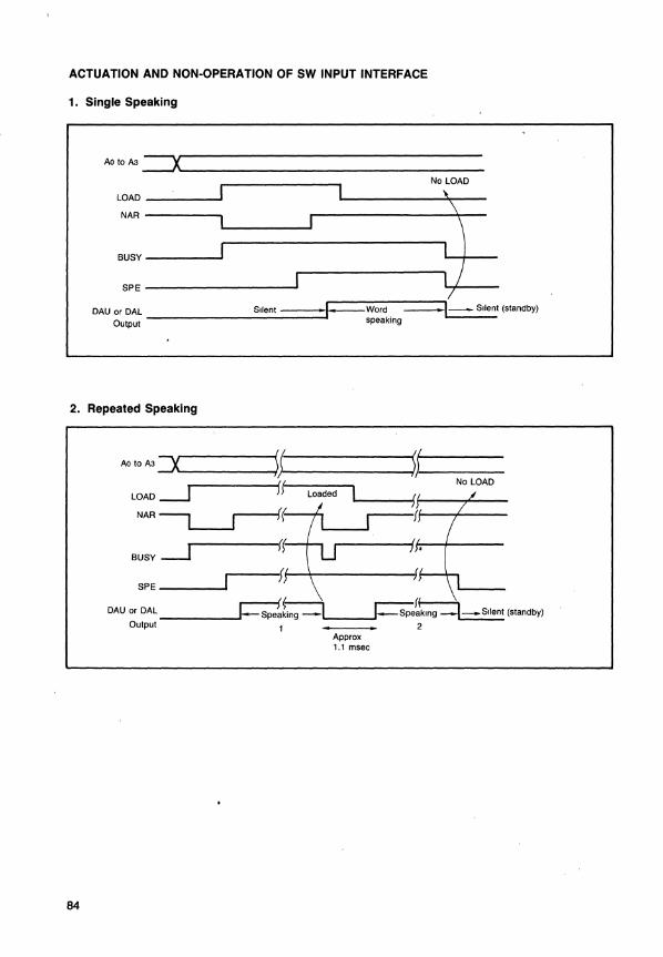
ACTUATION AND NON·OPERATION OF SW INPUT INTERFACE
1. Single Speaking
AO to A3 ::::x~ ............................................................................ -LOAD ................ _.J1 1 NAR ....................... 1 J
BUSY ____ --'1
No LOAD
It \
\
I
J 1,-,1 __ SPE-.......................................... 7
DAU or DAL Silent _!--Word. _1-- Silent (standby) Output _ ........................................ ---1 speaking
2. Repeated Speaking
84
,(-Ao to A3 =:x ........................ -l Il"
LOAD --.J if f(:-NAR ~L.._---I
r----1{(: BUSY --....l
),t
~--~f~~------~ SPE __ .... _-I
No LOAD
DAU or DAL ___ .... _.J~ting _I I_spe~klng :::J_Sllent (standby)
Output 1 2 Approx 1.1 msec
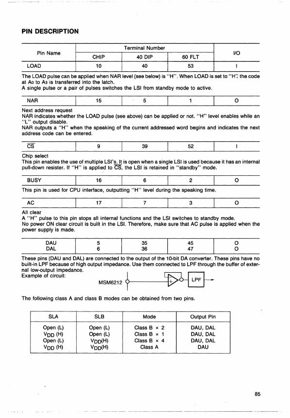
PIN DESCRIPTION
Terminal Number Pin Name
CHIP 40 DIP 60 FLT 1/0
LOAD 10 40 53 I
The LOAD pulse can be applied when NAR level (see below) is "H". When LOAD is set to "H': the code at Ao to A3 is transferred into the latch. A single pulse or a pair of pulses switches the LSI from standby mode to active.
NAR 15 5 o Next address request NAR indicates whether the LOAD pulse (see above) can be applied or not. "H" level enables while an "L" output disable. NAR outputs a "H" when the speaking of the current addressed word begins and indicates the next address code can be entered.
CS 9 39 52
Chip select This pin enables the use of multiple LSI's. It is open when a single LSI is used because it has an internal pull-down resister. If "H" is applied to CS, the LSI is retained in "standby" mode.
BUSY 16 6 2 o This pin is used for CPU interface, outputting "H" level during the speaking time.
AC 17 7 3 o All clear A "H" pulse to this pin stops all internal functions and the LSI switches to standby mode. No power ON clear circuit is built in the LSI. Therefore, make sure that AC pulse is applied when the power supply is made.
DAU DAL
5 6
35 36
45 47
o o
These pins (DAU and DAL) are connected to the output of the 10-bit DA converter. These pins have no built-in LPF because of high output impedance. Use them connected to LPF through the buffer of external low-output impedance. Example of circuit:
MSM6212 0-------1
The following class A and class B modes can be obtained from two pins.
SLA SLB Mode Output Pin
Open (L) Open (L) Class B x 2 DAU, DAL VDD (H) Open (L) Class B x 1 DAU, DAL Open (L) VDD{H) Class B x 4 DAU, DAL VDD (H) VDD{H) Class A DAU
85
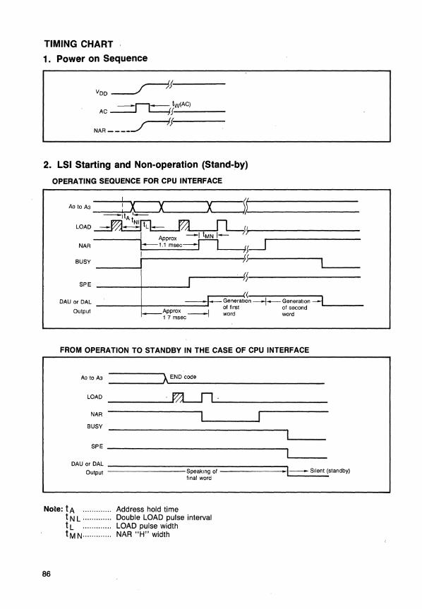
TIMING CHART
1. Power on Sequence
VDD~f 'n' :tW(AC)
AC f-----
NAR-- __ ~f
2. LSI Starting and Non-operation (Stand-by)
OPERATING SEQUENCE FOR CPU INTERFACE
Ao to A3
--~--LOAD
NAR
BUSY
SPE
X ,\ '-----...I~--~v~I------------
ff,I,-------
'--~H~ ~-------~5-----..., L-. __ _
~--~~----------------r---,---«--,.-----...,
DAU or DAL _____ +-_____ --' Generation -1-Generation --1 of first of second L-. __ _
Output _Approx _I word word 17 msec
FROM OPERATION TO STANDBY IN THE CASE OF CPU INTERFACE
AO to A3
LOAD
NAR
BUSY
_____ ~A~E_N_D_c_od_e ____________ __
--------~~----------------
SPE _________________ ~
DAUorDAL :==============~~~~=============t==~~~ Output Speaking of .1-Silent (standby) final word
Note: tA ............. Address hold time t N L ............. Double LOAD pulse interval t L ............. LOAD pulse width tMN ............. NAR "H" width
86
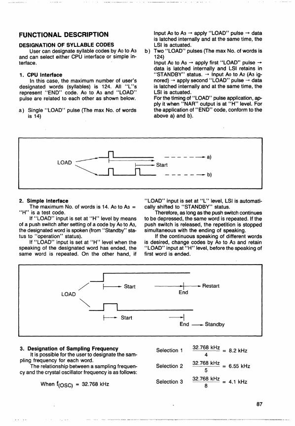
FUNCTIONAL DESCRIPTION
DESIGNATION OF SYLLABLE CODES User can designate syllable codes by Ao to A3
and can select either CPU interface or simple interface.
1. CPU Interface In this case, the maximum number of user's
designated words (syllables) is 124. All "L"s represent "END" code. Ao to A3 and "LOAD" pulse are related to each other as shown below.
a) Single "LOAD" pulse (The max No. of words is 14)
Input Ao to A3 -+ apply "LOAD" pulse -+ data is latched internally and at the same time, the LSI is actuated.
b) Two "LOAD" pulses (The max No. of words is 124) Input Ao to A3 -+ apply first "LOAD" pulse -+
data is latched internally and LSI retains in "STANDBY" status. -+ Input Ao to A2 (A3 ignored) -+ apply second "LOAD" pulse -+ data is latched internally and at the same time, the LSI is actuated. For the timing of "LOAD" pulse application, apply it when "NAR" output is at "H" level. For the application of "END" code, conform to the above a) and b).
LOAD -------D -------a) I .. ~ I---Start
~~ ------b)
2. Simple Interface The maximum No. of words is 14. Ao to A3 =
"H" is a test code. If "LOAD" input is set at "H" level by means
of a push switch after setting of a code by Ao to As, the designated word is spoken (from "Standby" status to "operation" status).
If "LOAD" input is set at "H" level when the speaking of the designated word has ended, the same word is repeated. On the other hand, if
~ / f---- Start
LOAD
"LOAD" input is set at "L" level, LSI is automatically shifted to "STANDBY" status.
Therefore, as long as the push switch continues to be depressed, the same word is repeated. If the push switch is released, the repetition is stopped simultaneous with the ending of speaking.
If the continuous speaking of different words is desired, change codes by Ao to A3 and retain "LOAD" input at "H" level, before the speaking of first word is ended.
.\ • Restart End
~~---------I---- Start
3. Designation of Sampling Frequency It is possible for the user to designate the sam
pling frequency for each word. The relationship between a sampling frequen
cy and the crystal oscillator frequency is as follows:
When f(OSC) = 32.768 kHz
--I End __ Standby
Selection 1
Selection 2
Selection 3
32.768 kHz = 8.2 kHz 4
32.768 kHz = 6.55 kHz 5
32.768 kHz = 4.1 kHz 8
87
STRAIGHT ADPCM AND COMPRESSED ADPCM
1. Straight ADPCM The features are enumerated below.
1. Length of ADPCM bits ..... fixed in 3 bits. 2. Deletion of silent component is possible. 3. High bit rate and high tone quality. 4. Suitable to imitation sound.
Example of bit rate fSAMPLE = 8.2 kHz Length of ADPCM bits = 3 bits Deleted silent component ~ 1/5 (speech)
B.R :; 8.2 x 3 x 4/5 =. 19.7 kb/sec
2. Compressed ADPCM The features are enumerated below:
1. Length of ADPCM bits ..... fixed in 3 bits 2. Deletion of data by repeated detection of
speech waveform 3. Deletion of silent component is possible. 4. Low bit rate. 5. Mainly applied to speech.
88
Example of bit rate fSAMPLE = 8.2 kHz Length of ADPCM bits = 3 bits Frequency of average repetition ~ 3
(Deleted data component of waveform ~ 1/3)
Deleted silent component =: 1/5 (speech) B.R lr 8.2 x 3 x 1/3 x 4/5 =. 6.6 kb/sec
SAMPLING FREQUENCY AND BAND WIDTH
1. Simple Relationship between Sampling Frequency and Band Width
fSAMPLE x 1/2 = fBAND (UL) Here tBAND (UL) ..... Upper limit of band
fSAMPLE fBAND Quality
8.2 kHz DC to 4.1 kHz Clear maximum in-telligibility
Female speech of 6.55 kHz DC to 3.2 kHz high tone sounds
nasal
Unclear both male
4.1 kHz DC to 2.0 kHz and female speeches sound nasal
2. The Relationship between a Sampling Frequency and LPF (low pass filter) The relationship between a sampling frequen
cy and LPF (low pass filter) is fSAMPLE x 1/2 = fc (cutoff frequency of ideal filter). However, realistically it is necessary to design' 'f c" to be lower than the above equation according to the skirt characteristics of filter. That is, the band will be further narrowed according to filter characteristics.
As an example, the fc and skirt characteristics of L.P.F. used for speech analysis by Oki are shown as follows.
Skirt fSAMPLE fc Charac- fBAND
teristics
8.2 kHz 3.4 kHz -48 dB/oct DC to 3.4 kHz
6.55 kHz 2.7 kHz -48 dB/oct DC to 2.7 kHz
4.1 kHz 1.7 kHz -48 dB/oct DC to 1.7 kHz
EXAMPLE OF OUTPUT INTERFACE
When connected to MSCl161 for Class B (for 3 V system only)
VDD
VDD
VCK
SPE DAU VCK
MSB 16 DAU DAL
MSC1161
6212 SP@
SP8 12
VDD
VSS SLA VDD' SLB
VDD
Note: C's are all 0.1 IlF.
Class A Output
VCK
SPE
MSB 6212
DAU
DAL Open
VSS SLAVDD'SLB
VSS
89
90
VOO
3/4 VOO
Class A OAU 1/2 VOO
1/4 VOO
VSS=O V
(
( Class B x 2
(8-bit OAC)
\
VOO
OAU
VSS
VOO
OAL
VSS
OAU
OAL
( DAU
Class B x 4
(7-bit OAC)
\ DAL
MSB "1" t
~ MSB "0"
MSB "1"
MSB "0"
MSB "1"
MSB "0"
MSB "1"
MSB "0"
(An abbreviated name of the type is sometimes used as an indication representing an actual product)
OKI semiconductor
MSM6308 ADPCM SPEECH PROCESSOR FOR SOLID STATE RECORDER DRAM INTERFACE
GENERAL DESCRIPTION
The Oki MSM630a is a ADPCM speech processor LSI for solid state recording which is manufactured using Oki's low power CMOS silicon gate technology. A maximum of 256K Dynamic RAM is used to store the ADPCM data.
The MSM630a has internal LPF and amplifier for a microphone. So, by connecting microphone, speaker, speaker driving amplifier and 256K DRAM, recording and playback of voice can be implemented in the same manner as a tape recorder.
FEATURES
• 4-bit ADPCM algorithm • Built-in a-bit AD converter • Built-in a-bit DA converter • Amplifier for microphone on chip • LPF (Low Pass Filter) on chip • 256K DRAM direct drive capability • Oscillation frequency: 4 MHz - 6 MHz
BLOCK DIAGRAM
RESET o----~
XT o---~
Xl' ()4---j
VCK ()4---i
NCR ()4---j
SAM o---~
START o----~ BUSY 0.---1
REC/PLAY 0---"
CSEL,
CSEL20---" CA,
CA2 o------<~
TEST,
TEST2
Timing and
Control
Channel Control
z ::J u:
• Sampling frequency: 4 kHz, a kHz (@ 4 MHz)
• Recording phrase: 1, 2, 4 selectable • Vocalization time: 16 sec. maximum
(@ 4 kHz) • Supply voltage: + 5 V • 44 pin plastic flat package
AOPCM AnalysIs! Systtiesis
10 to ..:J ..::l u: u::
z 15 <:
>:::> o <: o
VOD1
V002 V003 Analog voltage
VSS, VSS2 Analog ground
As
A7 I
A,
Ao
RAS CAS
WE
01/0
SG
SGC
91
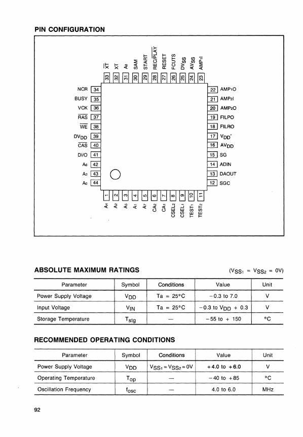
PIN CONFIGURATION
I- I~ I- en a:: w I- en en 0:: ~ <1: () en :::> en en
I~ I- < <1: I- W W () > :;;: ~ x en en a:: a:: u.. 0 <1:
NCR AMP10
BUSY AMP21
VCK AMP20
RAS FILPO
WE FILRO
OVOO VOO
CAS AVOO
0110 SG
A6 AOIN
A3 0 OAOUT
Ao SGC
J. .i{ .;;: ~ .:;: '" is '" .:i ~ ~ <1: ....J () W W en en en en w w
() () l- I-
ABSOLUTE MAXIMUM RATINGS (VSS1 = VSS2 = OV)
Parameter Symbol Conditions Value Unit
Power Supply Voltage VOO Ta = 25°C -0.3 to 7.0 V
Input Voltage VIN Ta = 25°C -0.3 to VOO + 0.3 V
Storage Temperature Tstg - -55 to + 150 °C
RECOMMENDED OPERATING CONDITIONS
Parameter Symbol Conditions Value Unit
Power Supply Voltage VOO VSS1 =VSS2 =OV +4.0 to +6.0 V
Operating Temperature Top - -40 to +85 °C
Oscillation Frequency losc - 4.0 to 6.0 MHz
92
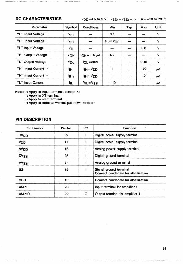
DC CHARACTERISTICS
Parameter Symbol
"H" Input Voltage ·1 VIH
"H" Input Voltage ·1 VIH
"L" Input Voltage VIL
"H" Output Voltage VOH
"L" Output Voltage VOL
"H" Input Current ·3 IIH1
"H" Input Current ·4 IIH2
"L" Input Current IlL
Note: ·1 Apply to input terminals except XT ·2 Apply to XT terminal ·3 Apply to start terminal
VDD=4.5 to 5.5 VSS1 =VSS2=OV TA= -30 to 70°C
Conditions Min Typ Max Unit
- 3.6 - - V
- 0.8xVOD - - V
- - - 0.8 V
10H= -40pA 4.2 - - V
IOL=2mA - - 0.45 V
IIH=VOD 1 - 100 pA
IIH=VDD - - 10 pA
VIL=VSS -10 - - pA
·4 Apply to terminal without pull down resistors
PIN DESCRIPTION
Pin Symbol Pin No. 1/0 Function
DVOD 39 I Digital power supply terminal
VDD' 17 I Digital power supply terminal
AVDD 16 I Analog power supply terminal
OVSS 25 I Digital ground terminal
AVSS 24 I Analog ground terminal
SG 15 I Signal ground terminal Connect condenser for stabilization
SGC 12 I Connect condenser for stabilization
AMP11 23 I Input terminal for amplifier 1
AMP10 22 0 Output terminal for amplifier 1
93
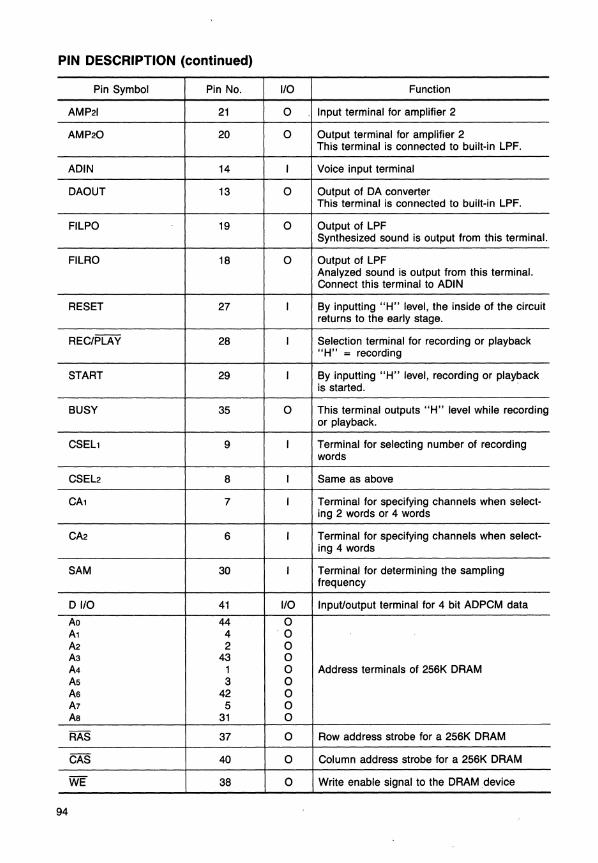
PIN DESCRIPTION (continued)
Pin Symbol Pin No. 110 Function
AMP21 21 0 Input terminal for amplifier 2
AMP20 20 0 Output terminal for amplifier 2 This terminal is connected to built-in LPF.
ADIN 14 I Voice input terminal
DAOUT 13 0 Output of DA converter This terminal is connected to built-in LPF.
FILPO 19 0 Output of LPF Synthesized sound is output from this terminal.
FILRO 18 0 Output of LPF Analyzed sound is output from this terminal. Connect this terminal to ADIN
RESET 27 I By inputting "H" level, the inside of the circuit returns to the early stage.
REC/PLAY 28 I Selection terminal for recording or playback "H" = recording
START 29 I By inputting "H" level, recording or playback is started. '
BUSY 35 0 This terminal outputs "H" level while recording or playback.
CSEL1 9 I Terminal for selecting number of recording words
CSEL2 8 I Same as above
CA1 7 I Terminal for specifying channels when select-ing 2 words or 4 words
CA2 6 I Terminal for specifying channels when select-ing 4 words
SAM 30 I Terminal for determining the sampling frequency
D 110 41 1/0 InpuUoutput terminal for 4 bit ADPCM data
Ao 44 0 A1 4 0 A2 2 0 A3 43 0 A4 1 0 Address terminals of 256K DRAM As 3 0 A6 42 0 A7 5 0 As 31 0
RAS 37 0 Row address strobe for a 256K DRAM
CAS 40 0 Column address strobe for a 256K DRAM
WE 38 0 Write enable signal to the DRAM device
94
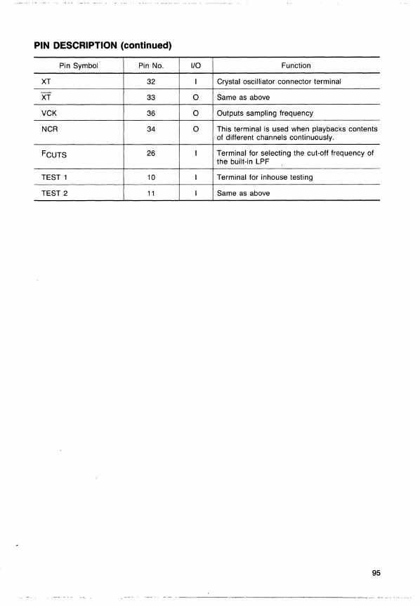
PIN DESCRIPTION (continued)
Pin Symbol Pin No. I/O Function
XT 32 I Crystal osciliiator connector terminal
-XT 33 0 Same as above
VCK 36 0 Outputs sampling frequency
NCR 34 0 This terminal is used when playbacks contents of different channels continuously.
FCUTS 26 I Terminal for selecting the cut-off frequency of the built-in LPF
TEST 1 10 I Terminal for inhouse testing
TEST 2 11 I Same as above
95
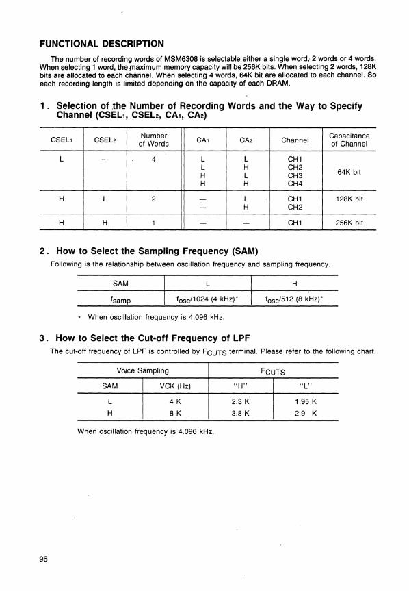
FUNCTIONAL DESCRIPTION
The number of recording words of MSM630B is selectable either a single word, 2 words or 4 words. When selecting 1 word, themaximum memory capacity will be 256K bits. When selecting 2 words, 12BK bits are allocated to each channel. When selecting 4 words, 64K bit are allocated to each channel. So each recording length is limited depending on the capacity of each DRAM.
1. Selection of .the Number of Recording Words and the Way to Specify Channel (CSEL1, CSEl2, CAl, CA2)
CSELl CSEL2 Number
CAl CA2 Channel Capacitance
of Words of Channel
L - 4 L L CH1 L H CH2
64K bit H L CH3 H H CH4
H L 2 - L CH1 12BK bit - H CH2
H H 1 - - CH1 256K bit
2. How to Select the Sampling Frequency (SAM) Following is the relationship between oscillation frequency and sampling frequency.
SAM L H
fsamp fosc/1024 (4 kHz)' fosc/512 (8 kHz)'
, When oscillation frequency is 4.096 kHz.
3. How to Select the Cut-off Frequency of LPF The cut-off frequency of LPF is controlled by FCUTS terminal. Please refer to the following chart
Vo,ice Sampling
SAM I VCK (Hz)
L
I 4K
H 8K
When oscillation frequency is 4.096 kHz.
96
"H"
2.3 K
3.B K
FCUTS
"L"
1.95 K
2.9 K
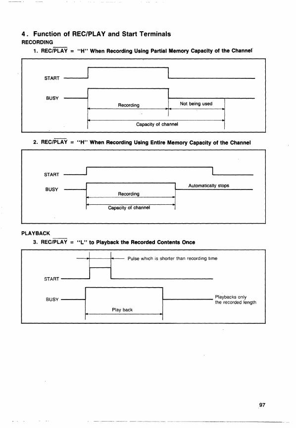
4. Function of REC/PLAY and Start Terminals RECORDING
1. REC/PLA Y = "H" When Recording Using Partial Memory Capacity of the Channel'
START
BUSY Recording Not being used
Capacity of channel
2. REC/PLAY = "H" When Recording Using Entire Memory Capacity of the Channel
START
BUSY Automatically stops
Recording
Capacity of channel
PLAYBACK
3. REC/PLAY = "L" to Playback the Recorded Contents Once
Pulse which is shorter than recording time
START
BUSY ~ .1
Playbacks only the recorded length
Play back
97
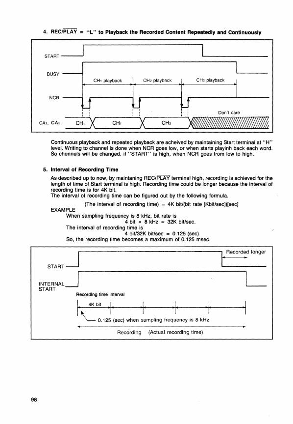
98
4. REC/PLAY = "L" to Playback the Recorded Content Repeatedly and Continuously
START I I BUSY I I
CH, playback CH2 playback CH2 playback .1
NCR I ,W ,L.j ,W , , , , , : Don't care , , , I
'X CA" CA2 CH, X CH, CH2 -Continuous playback and repeated playback are acheived by maintaining Start terminal at "H" level. Writing to channel is done when NCR goes low, or when starts playinh back each word. So chen nels will be changed, if "START" is high, when NCR goes from low to high.
5. Interval of Recording Time
As described up to now, by maintaning REC/PLAY terminal high, recording is achieved for the length of time of Start terminal is high. Recording time could be longer because the interval of recording time is for 4K bit. The interval of recording time can be figured out by the following formula.
(The interval of recording time) '" 4K bitl(bit rate (KbitlsecJ)[sec] EXAMPLE
When sampling frequency is 8 kHz, bit rate is 4 bit x 8 kHz '" 32K bit/sec.
The interval of recording time is 4 bitl32K bitlsec '" 0.125 (sec)
So, the recording time becomes a maximum of 0.125 msec.
START~' I' ReCOrd!d longer
INTERNAL~r--------------------------------------------~ __ __
START Recording time interval
I 4K bit I I I I .. 'I' " 1 r 1 " •
'- 0.125 (sec) when sampling frequency is 8 kHz •
Recording (Actual recording time)
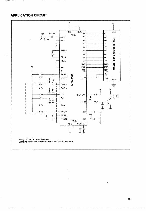
APPLICATION CIRCUIT
VOO1 Voo, VCC
~PF VOO, As As
AMP11 A7 A7 5 mV AMP10 A6 A6 ~ «
As As cr: A4
0 A4
~ AMP,I A3 A, <0
Lt)
A, A2 ~
FIL1N A1 A1 « CD In
FIL,O Ao Ao N -RAS RAS .... ::E
ADIN CAS CAS (J)
WE WE ::E
RESET GO 0
DIN
START CO) 01/0 °OUT VSS CD
::E (J)
CSEL1 ::E CSEL,
CA1 REC/PLAY ~I)) CA,
FIL10
SAM
I -=-
FCUTS XT
=l TEST1 0 TEST2 Xl
FIxing "L" or "A" level determlns Sampling frequency, number of words and cut-off frequency.
99
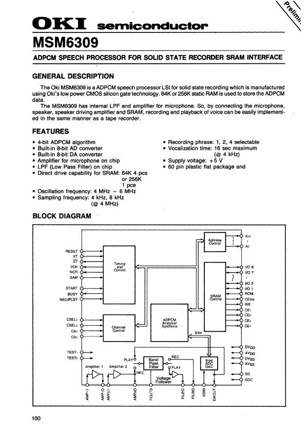
OKI semiconductor
MSM6309 ADPCM SPEECH PROCESSOR FOR SOLID STATE RECORDER SRAM INTERFACE
GENERAL DESCRIPTION
The Oki MSM6309 is a ADPCM speech processor LSI for solid state recording which is manufactured using Oki's low power CMOS silicon gate technology. 64K or 256K static RAM is used to store the ADPCM data.
The MSM6309 has internal LPF and amplifier for microphone. So, by connecting the microphone, speaker, speaker driving amplifier and SRAM, recording and playback of voice can be easily implemented in the same manner as a tape recorder.
FEATURES
• 4-bit ADPCM algorithm • Built-in a-bit AD converter • Built-in a-bit DA converter • Amplifier for microphone on chip • LPF (Low Pass Filter) on chip • Direct drive capability for SRAM: 64K 4 pes
or 256K 1 pce
• Oscillation frequency: 4 MHz - 6 MHz • Sampling frequency: 4 kHz, a kHz
(@ 4 MHz)
BLOCK DIAGRAM .
100
RESET o---~ XT o---~ Xfo.--~
VCK ()4----i NCR ()4----i SAM o---~
START o---~ BUSY o.--~
RECJPlJiV o---.j
CSEL. o---~ CSEL2 o---~
CA. o---~
CM o---~
TEST.
TEST,
Timing and
Control
Channel Control
• Recording phrase: 1, 2, 4 selectable • Vocalization time: 16 sec maximum
(@ 4 kHz) • Supply voltage: + 5 V • 60 pin plastic flat package and
ADPCM AnalYSIs! Syst~eslS
g 0u.~ Ii:
z is <
A ••
Ao
1108 1107
V02 I/O 1 ROM CE2sa WE
CEo CE,
CE, CE4
DVDD AVDD DVSS AVSS
SG
SGC
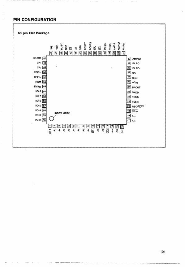
PIN CONFIGURATION
60 pin Flat Package
~ !U f!! III en 0 ~
I~ '" a: :E en => I~ I~
en 0:: 0:: 0 => 0 I~ ~ ~ w 0 1) ~ ::ii ::ii ::ii > ID Z a: LL « « «
START AMP20
CA, FILPO
CII:! FILRO
CSEL, SG
CSEL2 SGC ROM ADIN
DVDD BAOUT
1/08 AVDD
1107 TEST2
1/06 TEST,
1105 REC/PLAY
1/04 CE2 .. INDEX MARK
1/03
cf A,.
1/02 A'3
~ ~ « ~ ~ < .:l! .l! .< I~ .l! ~ I~ 0
~ N
g « «
101
ABSOLUTE MAXIMUM RATINGS (VSSl = VSS2 = OV)
Parameter Symbol Condition Value Unit
Power Supply Voltage VOO Ta = 25DC -0.3 to 7.0 V
Input Voltage VIN Ta = 25DC - 0.3 to VOO + 0.3 V
Storage Temperature Tstg - -55 to + 150 DC
RECOMMENDED OPERATING CONDITIONS
Parameter Symbol
Power Supply Voltage VOO
Operating Temperature Top
Oscillation Frequency fosc
DC CHARACTERISTICS
Parameter Symbol
"H" Input Voltage " VIH
"H" Input Voltage '2 VIH
"L" Input Voltage VIL
"H" Output Voltage VOH
"L" Output.Voltage VOL
"H" Input Current IIH1
"L" Input Current IlL
Note: " Apply to input terminals except XT '2 Apply to XT terminal
102
Condition Value Unit
VSS1 =VSS2 =OV +3.5 to +6.0 V
- -40 to +85 DC
- 4.0 to 6.0 MHz
VOO=4.5 to 5.5 VSS1 =VSS2 =OV Ta= -40-85DC
Condition Min Typ Max Unit
- 3.6 - - V
- 0.8xVOO - - V
- - - 0.8 V
IOH= -40pA 4.2 - - V
IOL=2mA - - 0.45 V
VIH=VOO 20 - 400 pA
VIL=VSS -10 - - pA
PIN DESCRIPTION
Pin Symbol Pin No. 110 Function
OVOO 53 I Oegital power supply terminal
AVOO 23 I Analog power supply terminal
OVSS 35 I Oegital ground terminal
AVSS 34 I Analog ground terminal
SG 27 I Signal ground terminal Connect condenser for stabilization
SGC 26 I Connect condenser for stabilization of SG
AMP11 33 I Input terminal for amplifier 1
AMP10 32 0 Output terminal for amplifier 1
AMP21 31 I Input terminal for amplifier 2
AMP20 30 0 Output terminal for amplifier 2 This terminal is connected to built-in LPF.
AOIN 25 I Voice input terminal
OAOUT 24 0 Output of OA converter This terminal is connected to built-in LPF.
FILPO 29 0 Output of LPF Synthesized sound is output from this terminal.
FILRO 28 0 Output of LPF Analized sound, original sound is output from this terminal
RESET 39 I By inputting "H" level, the inside of the circuit returns to the early stage, viz. stand-by stage
REC/PLAY 20 I Selection terminal for recording or playback "H" = recording
START 47 I By inputting "H" level, recording or playback is started
BUSY 44 0 This terminal outputs "H" level during recording or playback
CSEL1 50 I Terminal for selecting number of recording phrase
CSEL2 51 I Same as above
CA1 48 I Terminal for specifying channels when select-ing 2 phrases or 4 phrases
CA2 49 I Terminal for specifying channels when select-ing 4 phrases
SAM 40 I Terminal for determining the sampling frequency
103
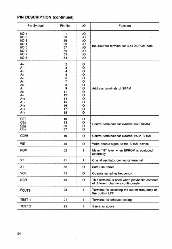
PIN DESCRIPTION (continued)
Pin Symbol Pin No. I/O Function
I/O 1 1 I/O I/O 2 60 I/O I/O 3 59 I/O I/O 4 58 I/O
Input/output terminal for 4-bit ADPCM data I/O 5 57 I/O I/O 6 56 I/O I/O 7 55 I/O I/O 8 54 I/O
Ao 2 0 A1 3 0 A2 4 0 A3 5 0 A4 6 0 As 7 0 As 8 0 A7 9 '0 Address terminals of SRAM As 11 0 A9 12 0 A10 14 0 An 15 0 A12 16 0 A13 17 0 A14 18 0
CE1 10 0 CE2 13 0 Control terminals for external 64K SRAM CE3 36 0 CE4 37 0
CE2ss 19 0 Control terminals for external 256K SRAM
WE 46 0 Write enable signal to the SRAM device
ROM 52 I Make "H" level when EPROM is equipped externally
XT 41 I Crystal oscillator connector terminal
XT 42 0 Same as above
VCK 45 0 Outputs sampling frequency
NCR 43 0 This terminal is used when playbacks contents of different channels continuously
FCUTS 38 I Terminal for selecting the cut-off frequency of the built-in LPF
TEST 1 21 I Terminal for inhouse testing
TEST 2 22 I Same as above
104
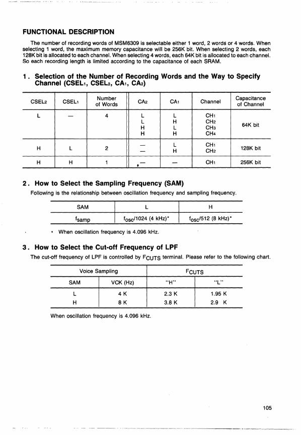
FUNCTIONAL DESCRIPTION
The number of recording words of MSM6309 is selectable either 1 word, 2 wordS or 4 words. When selecting 1 word, the maximum memory capacitance will be 256K bit. When selecting 2 words, each 128K bit is allocated to each channel. When selecting 4 words, each 64K bit is allocated to each channel. So each recording length is limited according to the capacitance of each SRAM.
1. Selection of the Number of Recording Words and the Way to Specify Channel (CSEL1, CSEL2, CA1, CA2)
CSEL2 CSEL1 Number CA2 CA1 Channel Capacitance
of Words of Channel
L - 4 L L CH1 L H CH2
64K bit H L CH3 H H CH4
H L 2 - L CH1 128K bit - H CH2
H H 1 • - - CH1 256K bit
2. How to Select the Sampling Frequency (SAM) Following is the relationship between oscillation frequency and sampling frequency.
SAM L H
fsamp fosc/1024 (4 kHz)' fosc/512 (8 kHz)'
, When oscillation frequency is 4.096 kHz.
3. How to Select the Cut-off Frequency of LPF The cut-off frequency of LPF is controlled by FCUTS terminal. Please refer to the following chart.
Voice Sampling FCUTS
SAM VCK (Hz) "H" "L"
L 4K 2.3 K 1.95 K
H 8K 3.8 K 2.9 K
When oscillation frequency is 4.096 kHz.
105
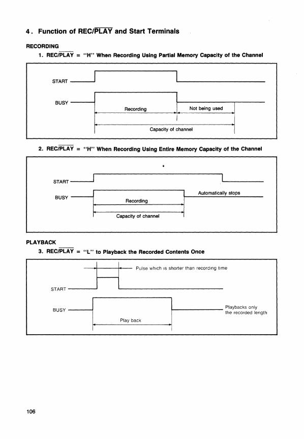
4. Function of REC/PLAY and Start Terminals
RECORDING
1. REC/PLAY = "H" When Recording Using Partial Memory Capacity of the Channel
START __ ....oJ
BUSY ----I Recording Not being used _I
Capacity of channel I
2. REC/PLAY ="H" When Recording Using Entire Memory Capacity of the Channel
START--....oJ
BUSY --:~: =====R=eco=rd~ing:======::1 Capacity of channel
Automatically stops
PLAYBACK
3. REC/PLAY = "L" to Playback the Recorded Contents Once
--1----+'-- Pulse which IS shorter than recording time
START -----'
BUSY
I. .1
Playbacks only the recorded length
Play back
106
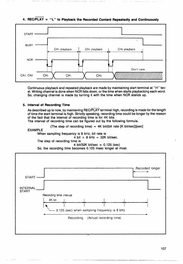
4. REC/PLAY = OIL" to Playback the Recorded Content Repeatedly and Continuously
STAR1 I I BUSY
, I CH, playback CH2 playback CH2 playback I
NCR I ,W ,W W , , I , , : Don't care , , , , ,
CA1, CA2 CH, X CH, X CHz -Continuous playback and repeated playback are made by maintaining start terminal at "H" level. Writing channel is done when NCR falls down, or the time when starts playbacking each word. So, changing channel is made by turning it with the time when NCR stands up.
5. Interval of Recording Time
As described up to now, by maintaning REC/PLAY terminal high, recording is made for the length of time the start terminal is high. Strictly speaking, recording time could be longer by the reason of the fact that the interval of recording time is for 4K bits. The interval of recording time can be figured out by the following formula.
(The step of recording time) = 4K bitl(bit rate [K bit/sec])[sec) EXAMPLE
When sampling frequency is 8 kHz, bit rate is 4 bit x 8 kHz = 32K bitlsec.
The step of recording time is 4 bitl32K bitlsec = 0.125 (sec)
So, the recording time becomes 0.125 msec longer at most.
START~ INTERNAL~'--------------------------------------------~ __ __
START Recording time interval
I_ 4K bit -I- ' I ' "" I, '- 0 125 (sec) when sampling frequency IS 8 kHz
-I
Recording (Actual recording time)
107
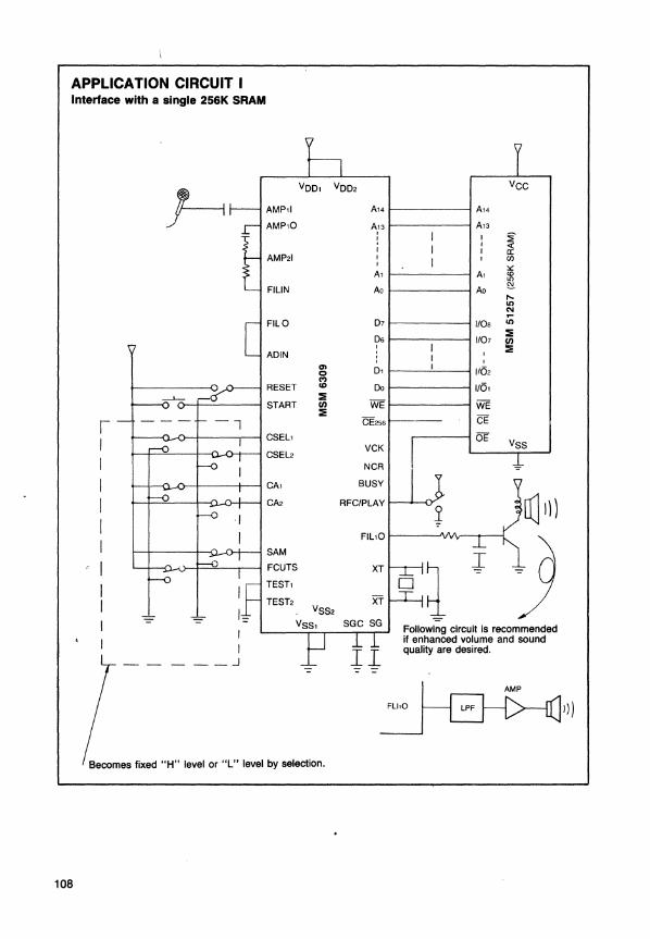
APPLICATION CIRCUIT I Interface with a single 256K SRAM
r I I I I I I I I I
1= - =
-- - __ .J
AMP11
AMP10
AMP21
FILIN
FILO
AOIN
RESET
START
CSEL1
CSEL2
CA,
CA2
SAM
FCUTS
TEST,
TEST2
VOO, vo02
A14
A'3 , :
A1
Ao
07
06
'" 0, C ..., CD Do :E en WE :E
CE256
VCK
NCR
BUSY
RFC/PLAY
FIL10
XT
XT VSS2
SGC SG
-=
Becomes fixed "H" level or "L" level by selection.
108
A14
An
~ « II: (J)
~ A1 <0 on Ao f;!..
"-Il) N ...
1/08 Il)
1/07 :E en :E ,
1/02
110,
WE
CE
OE VSS
~ll)
~ d J
0
Following circuit is recommended if enhanced volume and sound quality are desired.
AMP
FLI,Q I))
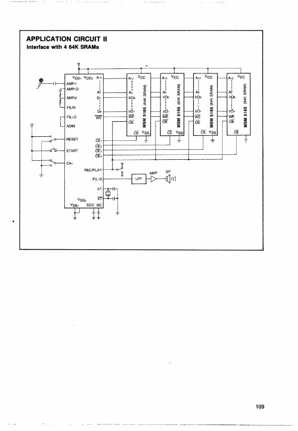
APPLICATION CIRCUIT II Interface with 4 64K SRAMs
~ Voo, VDO, A"
AMP,I , , ,
A~ AMP,' D; , FILIN I
I Do
FIL20 WE
RESET GE, CE2
START CE3 GE4
CA,
REC/PLAY
FIL,O
XT 0
Xi'
A" VCC I I I ~ I <t
Ao a: (J)
I/OB '" , ~ I
I
1/01 II) ., u;
WE
5E ::ii IJl ::ii
cr
~
1
A" VCC A12 VCC Ay VCC I I
~ , ,
~ I I ~ I I <t I <t A!
<t AD a: Ao a: a:
(J) (J) (J)
I/OB '" I/?B '" liP' '" ,
~ ,
~ I .. I ~
, I I I I It) I II) I II)
I/O, ., "0'
., 11O, .,
~ u; ~
WE II) WE WE II)
OE ::ii DE ::ii 5E ::ii IJl IJl IJl ::ii ::ii ::ii
II)
109
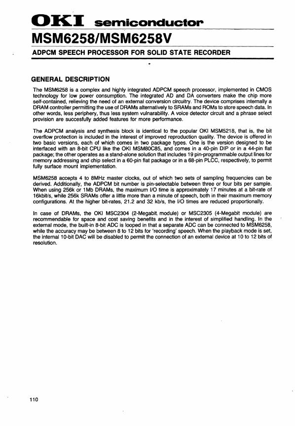
OKI semiconductor
MSM6258/MSM6258V ADPCM SPEECH PROCESSOR FOR SOLID STATE RECORDER
GENERAL DESCRIPTION
The MSM6258 is a complex and highly integrated ADPCM speech processor, implemented in CMOS technology for low power consumption. The integrated AD and DA converters make the chip more self-contained, relieving the need of an external conversion circuitry. The device comprises internally a DRAM controller permitting the use of DRAMs alternatively to SRAMs and ROMs to store speech data. In other words, less periphery, thus less system vulnarability. A voice detector circuit and a phrase select provision are succesfully added features for more performance.
The ADPCM analysis and synthesis block is identical to the popular OKI MSM5218, that is, the bit overflow protection is included in the interest of improved reproduction quality. The device is offered in two basic versions, each of which comes in two package types. One is the version designed to be interfaced with an 8-bit CPU like the OKI MSM80C85, and comes in a 40-pin DIP or in a 44-pin flat package; the other operates as a stand-alone solution that includes 19 pin-programmable output lines for memory addressing and chip select in a 60-pin flat package or in a 68-pin PLCC, respectively, to permit fully surface mount implementation.
MSM6258 accepts 4 to 8MHz master clocks, out of which two sets of sampling frequencies can be derived. Additionally, the ADPCM bit number is pin-selectable between three or four bits per sample. When using 256k or 1 Mb DRAMs, the maximum I/O time is approximately 17 minutes at a bit-rate of 16kbitls, while 256k SRAMs offer a little more than a minute of speech, both in their maximum memory configurations. At the higher bit-rates, 21.2 and 32 kb/s, the I/O times are reduced proportionally.
In case of DRAMs, the OKI MSC2304 (2-Megabit module) or MSC2305 (4-Megabit module) are recommendable for space and cost saving benefits and in the interest of simplified handling. In the external mode, the built-in 8-bit ADC is looped in that a separate ADC can be connected to MSM6258, while the accuracy may be between 8 to 12 bits for 'recording' speech. When the playback mode is set, the internal 10-bit DAC will be disabled to permit the connection of an external device at 10 to 12 bits of resolution.
110
FEATURES
• On chip analog I/O circuits: 8-bit ADC and 10-bit DAC
• ADC and DAC can be looped to connect external devices
• External conversion from 8 to 12 bits • Analog or PCM data input • Analog or PCM data output • Selectable voice detector function • On-chip complex memory timing & control • SRAM interface: 64 to 256kbit (128kbyte max) • Power-down mode possible with SRAM
interface • DRAM interface: 64K to 1 Mbit (2M byte max) • Internal DRAM controller/refresh circuit • Playback from programmed EPROMs • Master clock 4 to 8MHz (typically 4.096MHz) • Sampling frequencies 4.0, 5.3, and 8.0kHz
@4.096MHz clock • Selectable ADPCM bit numbers: 3 or 4-bit • Recording and playback monitor outputs • Momentary pause function during recording
and playback
• 7 phrase channels with individual length • Two versions: For stand-alone operation
For CPU interface (8-bit) • Four packaging options for flexible device
mounting • Single power supply + 5Volts (10%) • Current comsumption: 4mA (@4.096MHz)
10uA during standby (SRAM interface)
• Operational temperature - 40 to + 85°C (Stand-alone version)
• Operational temperature - 40 to + 85°C (MPU ifF version)
• Stand-alone version 60 pin plastic FLAT 68 pin PLCC (upon request only)
• MPU interface version 44 pin plastic FLAT 40 pin plastic DIP
111
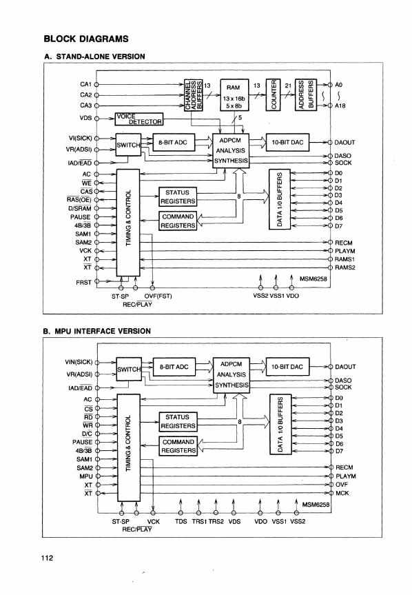
BLOCK DIAGRAMS
A. STAND-ALONE VERSION
CA1~----------------~
C~~--------------~
CA3~--------------~
AO
AlB
VDS
VI (SICK)
VR(ADSI)
IAD/EAD CD--;;;-~
AC WE CAS
RAS(OE) D/SRAM PAUSE
48/38
SAMl SAM2
VCK XT XT
FRST (I)---;;..~~
DAOUT
~--====~~ DASO ~~~1-~::::----~1S0CK
~--------------~ ~~----~DDO I-------(j) Dl ~-----"'O(])D2
~-----(j)D3
k'-----~O(]) D4 ~----(j)D5
~--------->~D6
k'---------->>{j) D7
~-r------------------------------------~~RECM
~~------------------------~PLAYM
~~----------------------------_(j)RAMSl
~-r-----------------------------------_(j)RAMS2
ST-SP OVF(FST) REC/PLAY
VSS2 VSSl VDO
B. MPU INTERFACE VERSION
112
VIN(SICK)
VR(ADSI) DAOUT
~-=====----.4 DASO IAD/EAD (I}-_---' ~--------------~~SOCK
AC CS RD WR D/C
PAUSE 48/38
SAMl SAM2 MPU
XT XT
~ ....... ......,..,....... i---------..<J) DO ~---?OO(])Dl
I-E----......... O(]) D2 ~----..<J) D3 ~---<>O(])D4
tE---------;.0(]) D5 ~------;~ D6 ~-------i>{]) D7
~~-----------------------~RECM
~~--------------------------------------~PLAYM
~~--------------------------~OVF
~~---------------------------~MCK
ST·SP VCK TDS TRS1TRS2 VDS VDO VSSl VSS2 REC/i'DiY
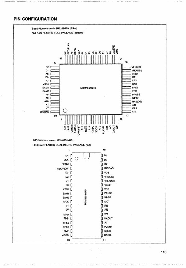
PIN CONFIGURATION
Stand-Alone version MSM6258GSK (GS-K)
6O-LEAD PLASTIC FLAT PACKAGE (bottom)
02
01
A6
DO A7
VSS1
SAM1
SAM2
A8
A9 A10
XT
XT
D/SRAM
60
MPU Intenace verSion MSM6258VRS
40-LEAD PLASTIC DUAL-IN-L1NE PACKAGE (top)
04
VCK
RECM
REC/PLAY
03
02
01
DO
VSS1
SAM1
SAM2
MCK
XT
Xl MPU
TDS
TRS2
TRS1
OVF
46/36
20
VI(SICK)
VR(ADSI)
VSS2 CA1
CA2
CA3
FRST
VDD
PAUSE
ST'SP
RAS(OE) A18
CAS A17
17
16
40
05
06
07
IAD/EAD
VDS
VI(SICK)
VRlADSI)
VSS2
VDD
PAUSE
ST·SP
ole RD
CS WR
DAOUT
AC
PLAYM
SOCK
DASO
21
113
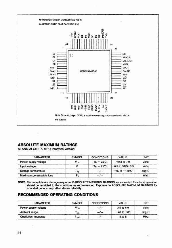
MPU interface version MSM6258VGS (GS-K)
44-LEAO PLASTIC FLAT PACKAGE (top)
£L ilj !.: 0 I~ 0 o:wu-v ~~~Bb
c ~ I-cc>o :$
44 34
33
03 0 NC
02 VI(AOSI)
01 VR(AOSI)
DO VSS2
VSSI VOO
SAMI MSM6258VGS-K PAUSE
SAM2 TSP
MCK DIG
XT RO
XT CS MPU WR
11 23
12 22
(J) iX en !:l; l[!l 0 0 !.: :::;; U ~ r=~~o~~~g~<Q
£L 0
Note: Since 17, 39 pIn (VOO') is substrate contInUIty, short-CircuIts wIth VOO in
the outside.
ABSOLUTE MAXIMUM RATINGS STAND-ALONE & MPU interface version
PARAMETER SYMBOL
Power supply voltage Voo
Input voltage V,
Storage temperature Tstg
Maximum permissable loss Pd
CONDITIONS VALUE
Ta = 25°C -0.3 to 7.0
Ta = 25°C -0.3 to VDD+0.3
-1- -55 to +1S00C
-1- 1
UNIT
Volts
Volts
deg C
Watt
NOTE: Permanent device damage may occur if ABSOLUTE MAXIMUM RATINGS are exceeded. Functional operation should be restricted to the conditions as recommended. Exposure to ABSOLUTE MAXIMUM RATINGS for extended periods may affect device reliability.
RECOMMENDED OPERATING CONDITIONS
PARAMETER SYMBOL CONDITIONS VALUE UNIT
Power supply voltage Voo -1- 3.5 to 6.0 Volts
Ambient range Top -1- -40 to +85 deg C
Oscillation frequency fose -1- 4 to 8 MHz
114
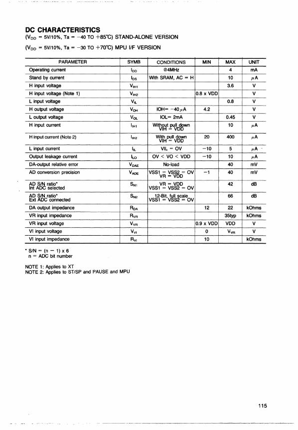
DC CHARACTERISTICS (VDD = 5V/10%, Ta = -40 TO +85·C) STAND-ALONE VERSION
(VDD = 5V110%, Ta = -30 TO +70·C) MPU IIF VERSION
PARAMETER SYMB CONDITIONS MIN MAX UNIT
Operating current IDD @4MHz 4 mA
Stand by current IDS With SRAM, AC = H 10 pA
H input voltage V,H1 3.6 V
H input voltage (Note 1) V,H2 0.8 x VDD V
L input voltage V,L 0.8 V
H output voltage VOH IOH= -401'A 4.2 V
L output voltage VOL IOL= 2mA 0.45 V
H input current I'HI Without pull down 10 I'A VIH = VDD
H input current (Note 2) I'H2 WJI~l,!;!IIJ8~n 20 400 I'A
L input current I'L VIL = OV -10 5 I'A
Output leakage current ILO OV < VO < VDD -10 10 I'A
DA-output relative error VDAE No-load 40 mV
AD conversion precision VADE VSS1 = VSS2 = OV -1 40 mV VR = VDD
AD SIN ratio' SNI VR = VDD 42 dB Int ADC selected VSS1 = VSS2 = OV
AD SIN ratio' SN2 12-Bit, full scale 66 dB Ext ADC connected VSS1 = VSS2 = OV
DA output impedance RDA 12 22 kOhms
VR input impedance RVR 35typ kOhms
VR input voltage VVR 0.9 x VDD VDD V
VI input voltage VVI 0 VVR V
VI input impedance RVI 10 kOhms
• SIN = (n - 1) x 6 n = ADC bit number
NOTE 1: Applies to XT NOTE 2: Applies to ST/SP and PAUSE and MPU
115
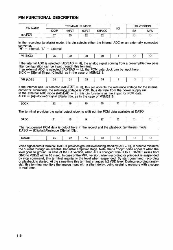
PIN FUNCTIONAL DESCRIPTION
TERMINAL NUMBER LSI VERSION PIN NAME I/O
40DIP I 44FLT I 60FLT I 68PLCC SA I MPU
IAD/EAD 37 I 35 I 32 I 62 I 0 I 0
In the recording (analysis) mode, this pin selects either the internal ADC or an externally connected converter. "H" = internal, "L" = external.
VI (SICK) 35 32 30 60 o o
If the internal ADC is selected (IAD/EAD = H), the analog signal coming from a pre-amplifier/low pass filter configuration can be input thrOimllJhis terminal. If an external ADC is selected (IAD/EAD = L), the PCM data clock can be input here. SICK = [S)erial [I)nput [C]loc[k), as in the case of MSM5218.
VR (ADSI) 34 31 29 59 o o
If the internal ADC is selected (IAD/EAD = H), this pin accepts the reference voltage for the internal converter. Nominally, the referen~oltage is VDD. thus derivale from the power supply rail. In the external ADC mode (IAD/EAD = L), this pin functions as the imput for PCM data. ADS I = [A)nalogue/[D)igital [S)erial [I)n, as in the case of MSM5218.
SOCK 22 19 10 38 o o
The terminal provides the serial output clock to shift out the PCM data available at DASO.
DASO 21 18 9 37 o o
The recuperated PCM data is output here in the record and the playback (synthesis) mode. DASO = [D)igital/[A)nalogue [S)erial [O)ut.
DAOUT 25 22 15 43 o o
o
o
o
Voice signal output terminal. DAOUT provides ground level during stand by (AC = H), in order to minimize the current through an eventual transistor amplifier stage. Note, that a "pop" noise appears when the level goes to ground. In case of the SA version, when AC is changed from H to L, DAOUT raises from GND to VDD/2 within 16 msec. In case of the MPU version, when recording or playback is suspended by stop command, this terminal maintains the level when suspended. By start command, recording or playback is started. At the same time this terminal changes 1/2 VDD level. During recording (analysis), this terminal monitors the analog input with a slight delay, being useful to measure with a scope in real time.
116
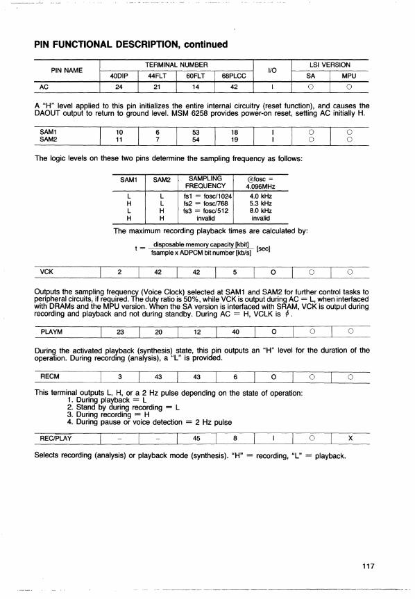
PIN FUNCTIONAL DESCRIPTION, continued
TERMINAL NUMBER LSI VERSION PIN NAME I/O
40DIP I 44FLT I 60FLT I 68PLCC SA I MPU
AC 24 I 21 I 14 I 42 I 0 I 0
A "H" level applied to this pin initializes the entire internal circuitry (reset function), and causes the DAOUT output to return to ground level. MSM 6258 provides power-on reset, setting AC initially H.
SAM1 SAM2
10 11
6 7
53 54
18 19
The logic levels on these two pins determine the sampling frequency as follows:
SAM1 SAM2 SAMPLING @fosc = FREQUENCY 4.096MHz
L L fs1 = fosc/1024 4.0 kHz H L fs2 = foscl768 5.3 kHz L H fs3 = foscl512 8.0 kHz H H invalid invalid
The maximum recording playback times are calculated by:
t = disposable memory capacity [kbit] [ ] fsample x ADPCM bit number [kb/s] sec
VCK 2 42 42 5 o
o o
o
o o
o
Outputs the sampling frequency (Voice Clock) selected at SAM1 and SAM2 for further control tasks to peripheral circuits, if required. The duty ratio is 50%, while VCK is output during AC = L, when interfaced with DRAMs and the MPU version. When the SA version is interfaced with SRAM, VCK is output during recording and playback and not during standby. During AC = H, VCLK is "'.
PLAYM 23 20 12 40 o o o
During the activated playback (synthesis) state, this pin outputs an "H" level for the duration of the operation. During recording (analysis), a "L" is provided.
RECM 3 43 43 6 o o o
This terminal outputs L, H, or a 2 Hz pulse depending on the state of operation: 1. During playback = L 2. Stand by during recording = L 3. During recording = H 4. During pause or voice detection = 2 Hz pulse
REC/PLAY 45 8 o x
Selects recording (analysis) or playback mode (synthesis). "H" = recording, "L" = playback.
117
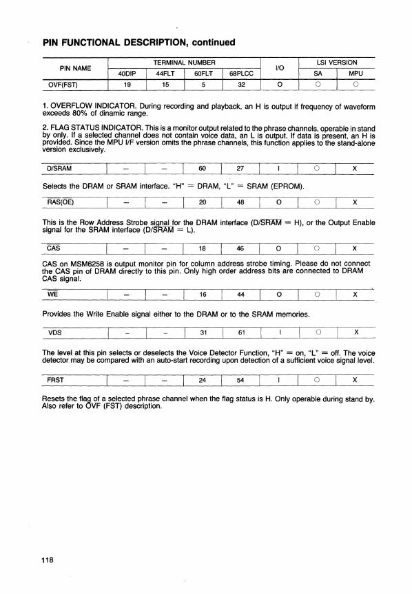
PIN FUNCTIONAL DESCRIPTION, continued
TERMINAL NUMBER LSI VERSION PIN NAME
I I I I/O
I 40DIP 44FLT 60FI..!T 68PLCC SA MPU
OVF(FST) 19 1 15 T 5 T 32 0 0 I 0
1. OVERFLOW INDICATOR. During recording and playback, an H is output if frequency of waveform exceeds 80% of dinamic range.
2. FLAG STATUS INDICATOR. This is a monitor output related to the phrase channels, operable in stand by only. If a selected channel does not contain voice data, an L is output. If data is present, an H is provided. Since the MPU IIF version omits the phrase channels, this function applies to the stand-alone version exclusively.
D/SRAM 60 27 o x
Selects the DRAM or SRAM interface. "H" = DRAM, "L" = SRAM (EPROM).
RAS(OE) 20 48 o o x
This is the Row Address Strobe s~nal for the DRAM interface (D/SRAM = H), or the Output Enable signal for the SRAM interface (DI RAM = L).
CAS 18 46 o o x
CAS on MSM6258 is output monitor pin for column address strobe timing. Please do not connect the CAS pin of DRAM directly to this pin. Only high order address bits are connected to DRAM CAS signal.
WE 16 44 o o x
Provides the Write Enable signal either to the DRAM or to the SRAM memories.
VDS 31 61 o x
The level at this pin selects or deselects the Voice Detector Function, "H" = on, "L" = off. The voice detector. may be compared with an auto-start recording upon detection of a sufficient voice signal level.
FRST 24 54 o x
Resets the flag of a selected phrase channel when the flag status is H. Only operable during stand by. Also refer to OVF (FST) description.
118
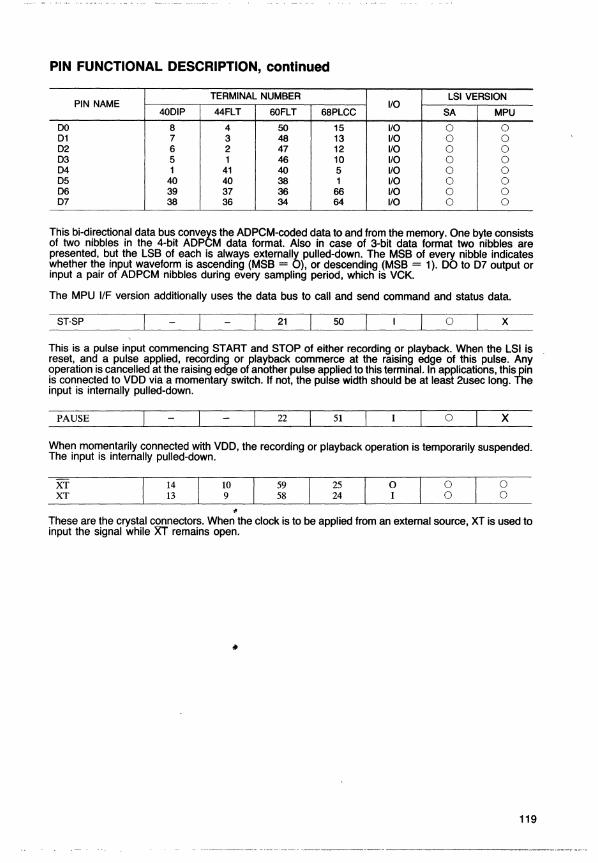
PIN FUNCTIONAL DESCRIPTION, continued
TERMINAL NUMBER LSI VERSION PIN NAME I/O
400lP 44FLT 60FLT 68PLCC SA MPU DO 8 4 50 15 I/O 0 0 01 7 3 48 13 I/O 0 0 02 6 2 47 12 I/O 0 0 03 5 1 46 10 I/O 0 0 04 1 41 40 5 I/O 0 0 05 40 40 38 1 I/O 0 0 06 39 37 36 66 I/O 0 0 07 38 36 34 64 I/O 0 0
This bi-directional data bus conveys the ADPCM-coded data to and from the memory. One byte consists of two nibbles in the 4-bit ADPCM data format. Also in case of 3-bit data format two nibbles are presented, but the LSB of each is always externally pulled-down. The MSB of every nibble indicates whether the input waveform is ascending (MSB = 0), or descending (MSB = 1). DO to 07 output or input a pair of ADPCM nibbles during every sampling period, which is VCK.
The MPU IIF version additionally uses the data bus to call and send command and status data.
ST·SP 21 50 o x
This is a pulse input commencing START and STOP of either recording or playback. When the LSI is reset, and a pulse applied, recording or playback commerce at the raising edge of this pulse. Any operation is cancelled at the raising edge of another pulse applied to this terminal. In applications, this pin is connected to VDD via a momentary switch. If not, the pulse width should be at least 2usec long. The input is internally pulled-down.
PAUSE 22 51 o x
When momentarily connected with VDD, the recording or playback operation is temporarily suspended. The input is internally pulled-down.
XT XT
14 13
10 9
1
59 58
25 24
o I
o o
o o
These are the crystal connectors. When the clock is to be applied from an external source, XT is used to input the signal while XT remains open.
119
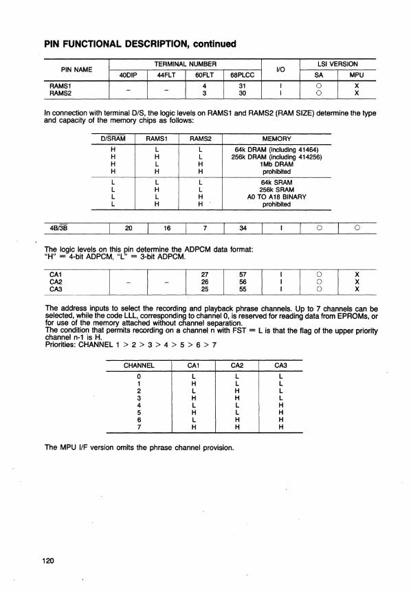
PIN FUNCTIONAL DESCRIPTION, continued
TERMINAL NUMBER LSI VERSION PIN NAME 110
40DIP 44FLT 60FLT 68PLCC SA MPU
RAMSl 4 31 I 0 X RAMS2 - - 3 30 I 0 X
In connection with terminal DIS, the logic levels on RAMS1 and RAMS2 (RAM SIZE) determine the type and capacity of the memory chips as follows:
D/SRAM RAMSl RAMS2 MEMORY H L L 64k DRAM (including 41464) H H L 256k DRAM (including 414256) H L H 1Mb DRAM H H H prohibited L L L 64k SRAM L H L 256k SRAM L L H AO TO A18 BINARY L H H prohibited
4B/3B 20 16 7 34 0 0
The logic levels on this pin determine the ADPCM data format: "H" = 4-bit ADPCM, "L" = 3-bit ADPCM.
CAl 27 57 0 X CA2 26 56 0 X CA3 25 55 0 X
The address inputs to select the recording and playback phrase channels. Up to 7 channels can be selected, while the code LLL, corresponding to channel 0, is reserved for reading data from EPROMs, or for use of the memory attached without channel separation. The condition that permits recording on a channel n with FST = L is that the flag of the upper priority channel n-1 is H. Priorities: CHANNEL 1 > 2 > 3 > 4 > 5 > 6 > 7
CHANNEL CAl CA2 CA3
0 L L L 1 H L L 2 L H L 3 H H L 4 L L H 5 H L H 6 L H H 7 H H H
The MPU ifF version omits the phrase channel provision.
120
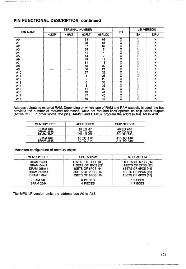
PIN FUNCTIONAL DESCRIPTION, continued
TERMINAL NUMBER LSI VERSION PIN NAME 1/0
40DIP 44FLT 60FLT 68PLCC SA MPU
AO 33 63 0 0 X Al 35 65 0 0 X A2 37 67 0 0 X A3 39 2 0 0 X A4 41 4 0 0 X A5 44 7 0 0 X A6 49 14 0 0 X A7 51 16 0 0 X A8 55 20 0 0 X A9 - - 56 21 0 0 X Al0 57 23 0 0 X All 1 28 0 0 X A12 2 29 0 0 X A13 6 33 0 0 X A14 8 35 0 0 X A15 11 39 0 0 X A16 13 41 0 0 X A17 17 45 0 0 X A18 19 47 0 0 X
Address outputs to external RAM. Depending on which type of RAM and RAM capacity is used, the bus provides the number of required addresses, while not required lines operate as chip select outputs (Active = 0). In other words, the pins RAMS1 and RAMS2 program the add tess bus AO to A18
MEMORY TYPE ADDRESSES CHIP SELECT
DRAM 64k AO TO A7 A8 TO A18 DRAM 256k AD TO A8 A9 TO A16 DRAM 1Mb AO TO A9 Al0 TO All SRAM 64k AO TO A12 A13 TO A18
SRAM 256k AO TO A14 A15 TO A18
Maximum configuration of memory chips:
MEMORY TYPE 4-BIT ADPCM 3-BIT ADPCM
DRAM 64kxl 11 SETS OF 8PCS [88J 11 SETS OF 6PCS [66J DRAM 64kx4 11 SETS OF 2PCS [22J 11 SETS OF 2PCS [22J
DRAM 256kxl 8SETS OF 8PCS [64J 8SETS OF 6PCS [48J DRAM 256kX4 8SETS OF 2PCS [16J 8SETS OF 2PCS [16J DRAM 1Mbxl 2SETS OF 8PCS [16J 2SETS OF 6PCS [12J
SRAM 64k 6 PIECES 6 PIECES SRAM 256k 4 PIECES 4 PIECES
The MPU IfF version omits the address bus AO to A 18.
121
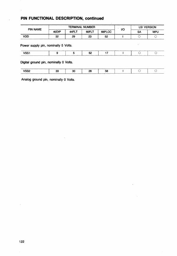
PIN FUNCTIONAL DESCRIPTION, continued
TERMINAL NUMBER - LSI VERSION PIN NAME I/O
40DIP I 44FLT I 60FLT I 68PLCC SA I MPU
VDD 32 I 29 I 23 I 52 I 0 I 0
Power supply pin, nominally 5 Volts.
VSS1 9 5 52 17 o o
Digital ground pin, nominally 0 Volts.
VSS2 33 30 28 58 o o
Analog ground pin, nominally 0 Volts.
122
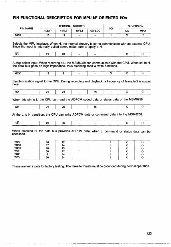
PIN FUNCTIONAL DESCRIPTION FOR MPU IIF ORIENTED 1I0s
TERMINAL NUMBER LSI VERSION PIN NAME 110
40DIP I 44FLT I 60FLT I 68PLCC SA I MPU MPU 15 I 11 I - I - I X I 0
Selects the MPU interface. When H, the internal circuitry is set to communicate with an external CPU. Since the input is internally pulled-down, make sure to apply a H.
CS 27 23 x o
A chip select input. When receiving a L, the MSM6258 can communicate with the CPU. When set to H, the data bus goes on high impedance, thus disabling read & write functions.
MCK 12 8 o X o
Synchronization signal to the CPU. During recording and playback, a frequency of fsample/2 is output here.
RD 28 24 46 X o
When this pin is L, the CPU can read the ADPCM coded data or status data of the MSM6258.
WR 26 25 48 X o
At the L to H transition, the CPU can write ADPCM data or command data into the MSM6258.
D/C 29 26 X o
When selected H, the data bus provides ADPCM data; when L, command or status data can be accessed.
TDS 16 12 I X 0 TRS1 17 14 I X 0 TRS2 18 13 I X 0 TSP 30 27 - - I X 0 TRP 4 44 I X 0 TVD 36 34 I X 0
These are test inputs for factory testing. The three terminals must be grounded during normal operation.
123
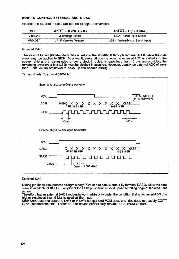
HOW TO CONTROL EXTERNAL ADC & DAC
Internal and external modes are related to signal conversion:
MODE IAD/EAD = H (INTERNAL) IAD/EAD = L (EXTERNAL)
VI (SICK) VI (Voltage Input) SICK (Serial Input Clock)
VR(ADSI) VR (Reference Voltage) ADSI (Analog/Digital Serial Input)
External DAC
The straight binary (PCM-coded) data is fed into the MSM6258 through terminal ADSI, while the data clock must be applied to SICK. As a result, every bit coming from the external ADC is shifted into the speech chip at the raising edge of every clock-in pulse. In case less than 12 bits are provided, the remaining lower order bits (LSB) must be clocked in as zeros. However, usually an external ADC of more than 8 bits will be employed to boost up the speech quality.
Timing charts (fosc = 4.096MHz)
External Analogue-Io-Digital converter
VCK
ADSI MSB 2SB 3SB4SB
SICK
>2us
External Digital-to-Analogue Converter
VCK ----.J DASO
SOCK
MSB2SB3SB
7.8 us -!--""*""""'foo!- 3.9 u s
DATA LATCHED L...----------f INTO MSM6258
LSB 10SB11SB
>2us
L SB
10SB11S
(lose = 4.096 MHz)
External DAC
During playback, recuperated straight binary PCM coded data is output by terminal DASO, while the data clock is available at SOCK. Every bit of the PCM pulse train is valid upon the falling edge of the clock-out pulses. The effort that an external DAC involves is worth while only under the condition that an external ADC of a higher resolution than 8 bits is used at the input. MSM6258 does not accept u-LAW or A-LAW companded PCM data, and also does not satisfy CCITT G.721 recommendation. Therefore, the device cannot fully replace an ADPCM CODEC.
124
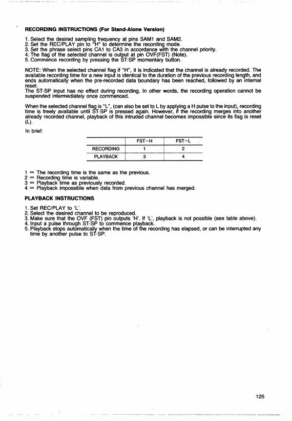
RECORDING INSTRUCTIONS (For Stand-Alone Version)
1. Select the desired sampling frequency at pins SAM1 and SAM2. 2. Set the REC/PLA Y pin to "H" to determine the recording mode. 3. Set the phrase select pins CA1 to CA3 in accordance with the channel priority. 4. The flag of the selected channel is output at pin OVF(FST) (Note). 5. Commence recording by pressing the ST·SP momentary button.
NOTE: When the selected channel flag if "H", it is indicated that the channel is already recorded. The available recording time for a new input is identical to the duration of the previous recording length, and ends automatically when the pre-recorded data boundary has been reached, followed by an internal reset. The ST·SP input has no effect during recording. In other words, the recording operation cannot be suspended intermediately once commenced.
When the selected channel flag is "L", (can also be set to L by applying a H pulse to the input), recording time is freely available until ST·SP is pressed again. However, if the recording merges into another already recorded channel, playback of this intruded channel becomes impossible since its flag is reset (L).
In brief:
FST=H
RECORDING 1
PLAYBACK 3
1 = The recording time is the same as the previous. 2 = Recording time is variable. 3 = Playback time as previously recorded.
FST=L
2
4
4 = Playback impossible when data from previous channel has merged.
PLAYBACK INSTRUCTIONS
1. Set REC/PLAY to 'L'. 2. Select the desired channel to be reproduced. 3. Make sure that the OVF (FST) pin outputs 'H'. If 'L', playback is not possible (see table above). 4. Input a pulse through ST·SP to commence playback. 5. Playback stops automatically when the time of the recording has elapsed, or can be interrupted any
time by another pulse to ST·SP.
125
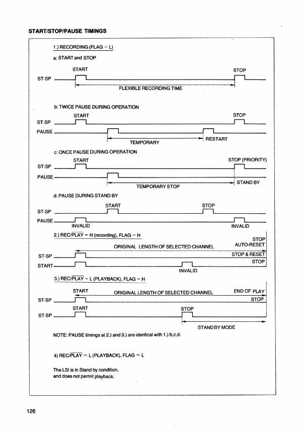
START/STOP/PAUSE TIMINGS
1.) RECORDING (FLAG = L)
a: START and STOP
START STOP
ST·SP ~ fI I
I • -: FLEXIBLE RECORDING TIME
b: TWICE PAUSE DURING OPERATION
START STOP
ST·SP !l n PAUSE fI n I. .. : RESTART
TEMPORARY
c: ONCE PAUSE DURING OPERATION
START STOP (PRIORITY)
ST·SP !l f1 PAUSE fI I .. .. ! STANDBY TEMPORARY STOP
d: PAUSE DURING STAND BY
START STOP ST·SP !l 11 PAUSE !l 11
INVALID INVALID
2.) REC/PLAY = H (recording), FLAG = H STOP
ORIGINAL LENGTH OF SELECTED CHANNEL AUTO-RESET
ST·SP 11 STOP & RESET
STOP START
INVALID
3.) REC/PLAY = L (PLAYBACK), FLAG = H
START ORIGINAL LENGTH OF SELECTED CHANNEL ENDOF PLAY
ST·SP 11 STOP
START STOP
ST·SP ~iIE ..
STANDBY MODE
NOTE: PAUSE timings at 2.) and 3.) are identical with 1.) b,c,d.
4) REC/PLA Y = L (PLAYBACK), FLAG = L
The LSI is in Stand by condition,
and does not permit playback.
126
POWER-DOWN REDUCTION MODE
During stand by, the internal oscillation circuit automatically stops the operation and validates the power-saving mode. This mode can be entered under the condition that the SRAM interface is set (D/S = L).when the master clock is 4.096MHz, the start-up period after cancellation of the power-saving mode by a START pulse lasts 20 to 30 ms until the oscillator stabilizes.
HOW TO USE PHRASE CHANNEL "0" (Stand-Alone Version)
[1]. Phrase channel "0" is effective for reading EPROM resident ADPCM coded speech data into the MSM6258. The EPROMs may have been programmed previously by a SAS1A or AW101 development system. When channel "0" is selected (CA1 to CA3 = L L L), all address outputs from AO to A18 are initialized to all "0", and commence counting up the ~na;gaddresses upon receipt of a pulse to the START input. Condition: RAMS1 = L, RAMS2 = H, 0/ RA = L; refer to pin descriptions. Playback of certain words or word groups can be implemented by external individual control of the CE inputs of the EPROMs. However, this demands adequate editing of speech data prior to writing the EPROMs. In the interest of best reproduction, the MSM6258 should be set at the same sampling rate at which the data was recorded and stored in the memories. When channel "0" is selected VDS (voice detector) input goes to L.
PLAYBACK INSTRUC'rIONS:
a. Set "REC/PLAY" to "L". b. Select channel 0 by setting CA 1 to CA3 to "L L L". c. Make sure that "OVF/FST" output is H, otherwise playback is impossible. If necessary, reset the chip. d. Apply a pulse to "ST·SP", and playback commences. e. Suspend playback with another pulse to START/STOP.
[2]. When DRAM or SRAM memories are interfaced with MSM6258, the selection of channel 0 gives the user the totally available memory area without channel separations.
SPEECH DEVELOPMENT SYSTEMS
Right top: SAS1 A records, replays, edits speech 00010203 04050607 data, and writes ADPCM coded data into 64 to
}M6258 128k EPROMs. It also copies written EPROMs. n I I n+1
A microphone and a line input are provided. n+2 I I n+3 Right bottom: The latest development system AW101 performs the same functions as SAS1 A,
} SAS but can be linked with a floppy drive, and has a n+1 I ! n
HEX keyboard for comfortable operation. It n+3 II n+2 writes EPROM's from 64k to 512k.
127
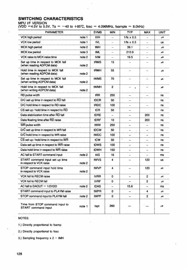
SWITCHING CHARACTERISTICS MPU IIF VERSION (VDD =4.SV to S.SV, Ta = -40 to +8S·C, fose = 4.096MHz, fsample = 8.0kHz)
PARAMETER
VCK high period
VCK low period
MCK high period
MCK low period
VCK raise to MCK raise time
Set up time in respect to MCK fall (when reading ADPCM data)
Hold time in respect to MCK fall (when reading ADPCM data)
Set up time in respect to MCK fall (when writing ADPCM data)
Hold time in respect to MCK fall (when writing ADPCM data)
RD pulse width
D/C set up time in respect to RD fall
D/C hold time in respect to RD raise
CS set up I hold time in respect to RD
Data stabilization time after RD fall
Data floating time after RD raise
WR pulse width
D/C set up time in respect to WR fall
D/C hold time in respect to WR raise
CS set up I hold time in respect to WR
Data set up time in respect to WR raise
Data hold time in respect to WR raise
AC fall to START command input
START command input set up time in respect to VCK raise
STOP command input hold time in respect to VCK raise
VCK fall to RECM raise
VCK fall to RECM fall
AC fall to DAOUT = 1/2VDD
START command inputto PLA YM raise
STOP command input to PLA YM fall
Time from STOP command input to START command input
NOTES:
1.) Directly proportional to fsamp
2.) Directly proportional to fosc
3.) Sampling frequency x 2 - tMH
128
note 1
note 1
note 2
note 3
note 2
note 2
note 2
note 2
note 2
note 2
note 2
note 2
note 2
note 2
note 1
SYMB MIN TYP
tVH - 1lfs x 0.5
tVL - 1lfs x 0.5
tMH - 39.1
tML - 210.9
tVM - 19.5
tRMS 15 -
tRMH 55 -
tWMS 70 -
tWMH 2 - • tRR 250 -
tDCR 50 -tRDC 100 -tCR 50 -
tORE - -tDRF 10 -tWW 250 -tDCW 50 -
tWDC 100 -
tCW 50 -tOWS 100 -
tDWH 150 -lAS 16 -
tWVS 4 -
tWVP 4 -
tVRR 0 -tVRF 0 -tDAS - 15.6
tWPR 0 -tWPF 0 -
tspt 260 -
MAX UNIT
- p.S
- us
- ~s
- ~s
- p.S
- ~s
- p.S
- ~s
- p.S
- ns
ns
- ns
ns
200 ns
200 ns
- ns
- ns
- ns
- ns
- ns
- ns
- ms
120 us
120 ~s
2 ~s
2 ~s
- ms
4 ~s
2 ~s
- p.S
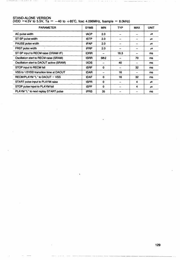
STAND-ALONE VERSION (VOO =4.5V to 5.5V, Ta = -40 to +85·C, fosc 4.096MHz, fsample = 8.0kHz)
PARAMETER SYMB MIN TYP MAX UNIT
AC pulse width tACP 2.0 - - ~s
ST·SP pulse width tSTP 2.0 - - ~
PAUSE pulse width tPAP 2.0 - - ~
FRST pulse width tFRP 2.0 - - ~s
ST·SP input to RECM raise (DRAM I/F) tORR - 16.3 - ms
Oscillation start to RECM raise (SRAM) tSRR 5&>2 - 70 ms
Oscillation start to DAOUT active (SRAM) tXDS - 40 - ms
STOP input to RECM fall tSRF 0 - 32 ms
VSS to 1/2VDD transition time at DAOUT tDAR - 16 - ms
RECM/PLAYM "L" to DAOUT = VSS tDAF 0 16 32 ms
START pulse input to PLA YM raise tSPR 0 - 4 ~
STOP pulse input to PLA YM fall tSPF 0 - 4 ~s
PLAYM "L" to next replay START pulse tPRS 35 - - ms
129
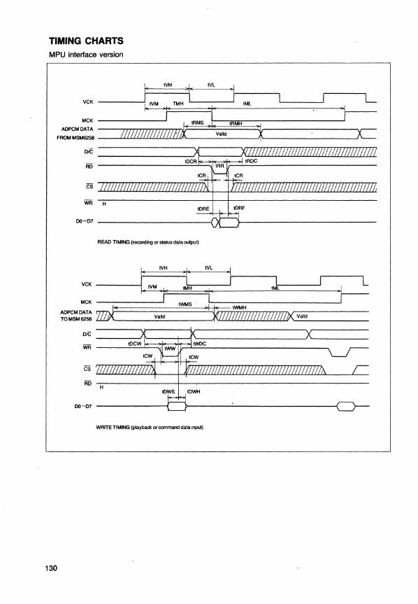
TIMING CHARTS MPU interface version
________ ~I TMH I~----~I j ... tVM iii> IE' tMl ",I
VCK
I I i MCK --------' ~~. tRMS _ !-1.-...,t:;.;;RMrT.H..,.----------~
F:~:~~:~ IVO!/! /Owl/lili .. -ValkJ 1----------'C
L
OIC __________ ../ )--____ -:''-'w.Lu..LLI...1..I..J.../..I..J.../...LJ..J...LJ..J...LJ..J..LLI...LJ..J...LLJ..I..J.../.~l.L
RO _________ ~t~OC~R~=t~tRrnR~~~~--------------
WR ~-----------+-~~----------------
00-07 ___________ --{
READ TIMING (recording or status data output)
I_ tVH _I" tVL ,I
I I I I VCK --------l tVM I tMH tML I
~ .. ~~-.~E======~·tIE~-----~~-----_1. MCK ---r;~~~~;;;;'~I==~~~I~~~~::;::::::===~r--tWMS I ~t. . ~ tWMH
~~p~::~~ WiA _____ --'V.::;:all.:..d ___ ~f..OIV7!OO0l701111JX'-v_al_ld _____ _
L
OIC ------/1'---,-+--1''--------------1 '--____ _
WR
00-07
WRITE TIMING (playback or command data Input)
130
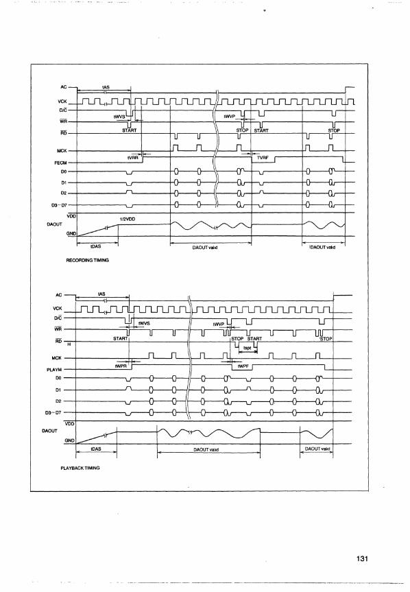
AC lAS
VCK
O/C
ViR
AD
MCK
FECM
DO
01
02
03-07
OAOUT
DAOUTvaild IDAOUTvalld
RECORDING TIMING
AC lAS
VCK
DlC
ViR
AD H
MCK
PLAYM
DO
01
02
03-07
OAOUT
tOAS DAOUTvahd OAOUTvalid
PLAYBACK TIMING
131
--- -------. --------~------- ----------------
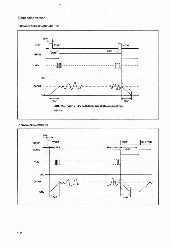
Stand-alone version
1.Recordlng Timing, DRAM IIF, VDS ~ "l"
SPSP STOP
ISRF -,,/---1--RECM
VCK - - - - - -JUUL- ----------------------------ft ---------
VDD--~-------------------------------4----------
DAOUT
GND'-4~---4-----------------------------------4~--~~--
IDAR
NOTE: When "VDS" IS H, the pIn RECM outputs a 2-Hz pulse during voice
delection.
IDAF
2. Playback TimIng (DRAM IIF)
SPSP START
---+t----ISPR ISPF --..... -+<---------1 PLAYM I r------------------------------------~~ ~-----
VCK - - - - - -JUUl- -----------------------c - - - -JU1ll -------------------
VDD--4--------------------------------------4------------------
DAOUT
GND---*----~------------------------------------+_~~~~~~------
IDAR IDAF
132
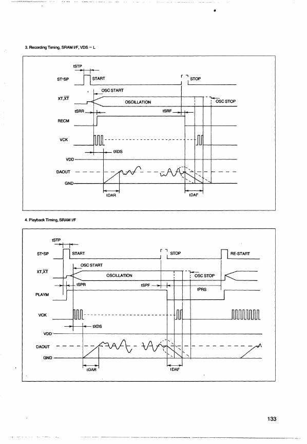
3. Recording Timing, SRAM IIF, VDS ~ L
tSTP
"j I' ST'SP ~L.S_T_A_RT ____________ ~
OSCSTART
~ STOP
XT,Xl __ --------------------------r---~~-~ : OSCSTOP
tSRF
RECM
VCK
VDD------~----------------------_+--+__r_+--------
GND-----~~-+_---------_+~~~~~-----
IOAR lOAF
4. Playback Timing, SRAM IIF
tSTP
"j I" ST'SP n START r , STOP n RE-START ~ I ________________________ ~I. LI ______________ ~ ..
OSCSTART
XT,Xl __ -----------------~--_r_.-~ OSCILLATION OSCSTOP
tSPF ~O+-+<--+--+--+--------__I tPRS
PLAYM
VCK
VDD·'----------r---------------------------+_-+~--+_-----------------------
DAOUT
GND---------1L----+----------------------~~~-'~----------------~------
tDAR lOAF
133
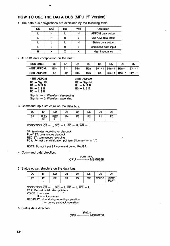
•
HOW TO USE THE DATA BUS (MPU IIF Version)
1. The data bus designations are explained by the following table:
CS D/C RD WR Operation
L H L H ADPCM data output
L H H L ADPCM data input
L L L H Status data output
L L H L Command data input
H X X X High impedance
2. ADPCM data composition on the bus:
BUS LINES:
4-BIT ADPCM:
3-BIT ADPCM:
4-BIT ADPCM
83 = Sign Bit B2=MSB B1 = 2 S B BO=LSB
DO D1
BOn B1n
XX BOn
Sign bit = 1: Waveform descending Sign bit = 0: Waveform ascending
D2 D3
B2n B3n
B1n B2n
3-BIT ADPCM 82 = Sign bit B1 = M S B BO=LSB
3. Command input structure on the data bus:
DO D1 D2 D3 D4 D5
SP PLAY REC P4 P3 P2 ST ST
CONDITION: CS = L, D/C = L, RD = H, WR = L
SP: terminates recording or playback PLAY ST: commences playback REC ST: commences recording
D4
BOn+1
XX
D6
P1
PO to P4: set the initialization pOinters. (Normaly set to "L")
NOTE: Do not input SP command during PAUSE.
4. Command data direction: command
CPU • MSM6258
5. Status output structure on the data bus:
DO D1 D2 D3 D4 D5
r:'O P1 P2 P3 P4 XX
CONDITION: CS = L, D/C = L, RD = L, WR = L PO to P4: set initialization pointers VOICE: L = mute '
H = voice present REC/PLAY: H = during recording operation
L = during playback operation
6. Status data direction: status
D6
VOICE
CPU • MSM6258
134
D5
B1n+1
BOn+1
D7
PO
D7
RECI PLAY
,
D6 D7
B2n+1 83n+1
B1n+1 82n+1
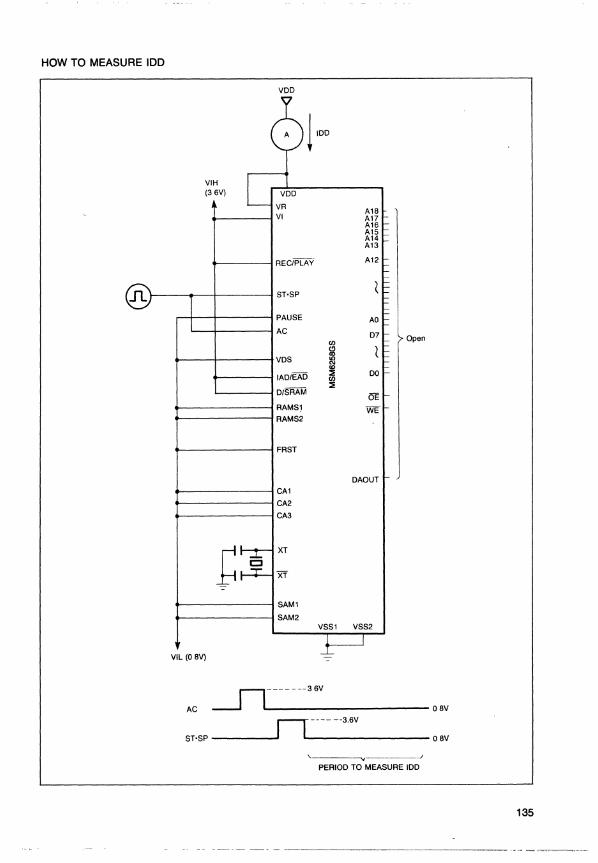
HOW TO MEASURE IDD
VDD
A 1 100
VIH L (36V) VDD
VR A18
VI A17 A16 A'S A14 A13
--~ A12 REC/PLAY
n ST'SP ( 1=
1 PAUSE AO f-I AC D7
en Open C!l l f-ClO
VDS It)
'" f-<0
IAD/EAD ::;: DO f-en ::;:
DIS RAM 5Ef-RAMSI WE RAMS2
FRST
DAOUT
CAl
CA2
CA3
tl= XT
XT
-=-SAMI
SAM2 VSSI VSS2
VIL (08Vj }--=--=-I
AC
~-------36V
o 8V _____ ~n-- --- --3.6V ST'SP • L. ___________ 08V
,---_v-___ J
PERIOD TO MEASURE 100
135
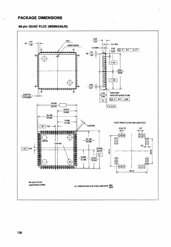
PACKAGE DIMENSIONS
68-pln QUAD PLCC (MSM6258JS)
136
45'~ 1,45
O,50lYP
3 PLACES
R1h (JA) 53'C/W Lead frame:CUIAIIoy
25,020
25,270
24,130
PIN 1
INDEX MARK
B-C 0,177 I
0,66
0,81 ·--r-1-:'·~1~-'--_-1-
12,510
12,635
FooT·PRINT LAYOUT 88-LEAD PLCC
'fl-fI-B-23,12
ALLDIMENSIONS ARE IN MILLIMETERS ~
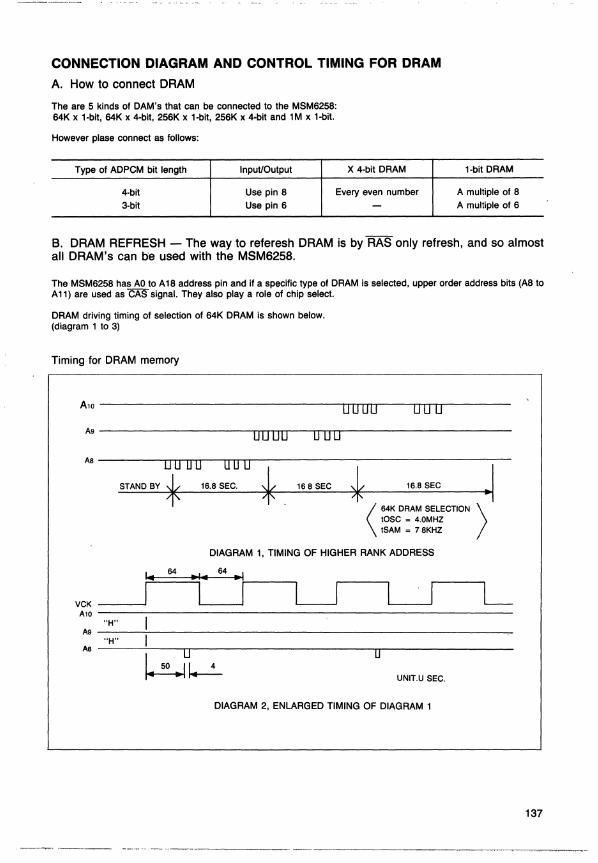
CONNECTION DIAGRAM AND CONTROL TIMING FOR DRAM
A. How to connect DRAM
The are 5 kinds of DAM's that can be connected to the MSM6258: 64K x 1-bit, 64K x 4-bit, 256K x 1-bit, 256K x 4-bit and 1M x 1-bit.
However plase connect as follows:
Type of ADPCM bit length Input/Output X 4-bit DRAM
4-bit Use pin 8 Every even number
3-bit Use pin 6 -
1-bit DRAM
A multiple of 8 A multiple of 6
B. DRAM REFRESH - The way to referesh DRAM is by RAS only refresh, and so almost all DRAM's can be used with the MSM6258.
The MSM6258 has AD to A18 address pin and if a specific type of DRAM is selected, upper order address bits (A8 to A 11) are used as CAS signal. They also playa role of chip select.
DRAM driving timing of selection of 64K DRAM is shown below. (diagram 1 to 3)
Timing for DRAM memory
A1O------------------------------~OTrrO~O~O.----nD'Dno~--------
A9--------------------~O~O~O~O~--~D~O~O~---------------------
M--------U~O~U~D~~U~D~O~~----------------------------I--
''''NO'' t ,.., ",c. Jtf '" "'C *' '" '"C •
VCK A10 "H" A9 "H" As
I.,. 64
< 64K DRAM SELECTION > IOSC = 4.0MHZ ISAM = 78KHZ
DIAGRAM 1, TIMING OF HIGHER RANK ADDRESS
~I .. 64 ~I
I I
o
L
I hn ~ ~~ UNIT.U SEC.
DIAGRAM 2, ENLARGED TIMING OF DIAGRAM 1
137
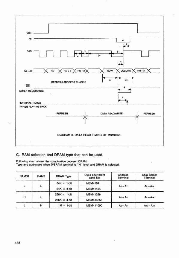
VCK
AS 4
RAS
AO-A7 ___ ~ '-.:.::..:_./ ,-...:..::..:..:..:..-/
REFRESH ADDRESS CHANGE I- 8 12 ~I
I-8
~ WE
(WHEN RECORDING)
~ INTERNAL TIMING (WHENP~Y~I~NG~B~A~CK~)--------------------~L-------------
REFRESH DATA READIWRITE REFRESH
DIAGRAM 3, DATA READ TIMING OF MSM6258
C. RAM selection and DRAM type that can be used.
Following chart shows the combination between DRAM Type and addresses when D/SRAM terminal is "H" level and DRAM is selected.
RAMSl RAM2 DRAM Type Oki's equivalent Address Chip Select parts No. Terminal Terminal
64K xl-bit MSM4164 L L Ao-A7 A8-A18
64K x 4-bit MSM41464
256K x l-bi! MSM41256 H L Ao-A8 Ag-A16
256K x 4-bit MSM414256
L H 1M xl-bit MSM411000 Ao-Ag AlO-All
138
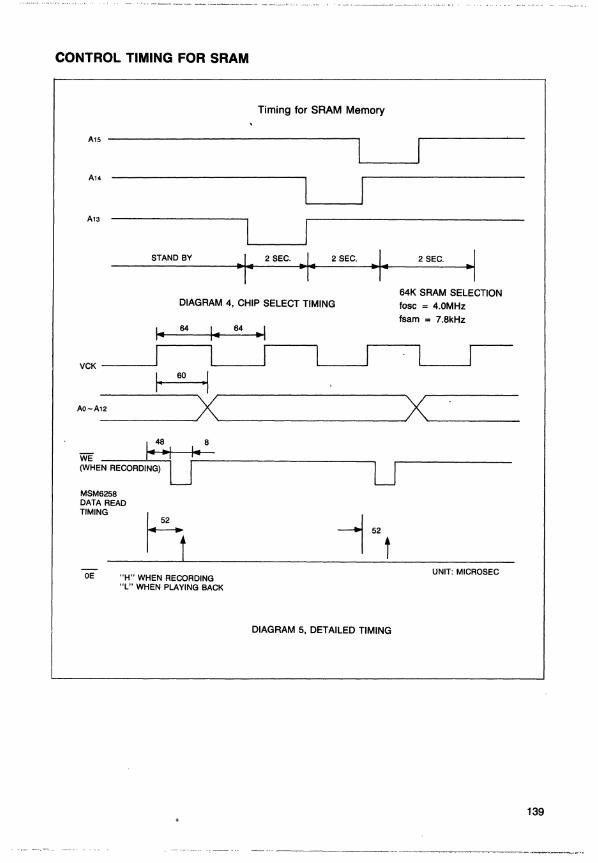
CONTROL TIMING FOR SRAM
Timing for SRAM Memory
A15 -------------------.1
A14
I A13
STAND BY 2 SEC. 2 SEC.
DIAGRAM 4, CHIP SELECT TIMING
vcK----~~1 ----~I----~I----~----~
2 SEC. ~I 64K SRAM SELECTION lose = 4.0MHz
Isam = 7.8kHz
I. 60 .1 AO-Al-2---~--~~~ _____________ ~~~ _____ __
I 48 8
WE" ~Oi--I" _____ ---, (WHEN RECORDING) U MSM6258 DATA READ TIMING
OE "H" WHEN RECORDING "L" WHEN PLAYING BACK
52
t
DIAGRAM 5, DETAILED TIMING
UNIT: MICROSEC
139
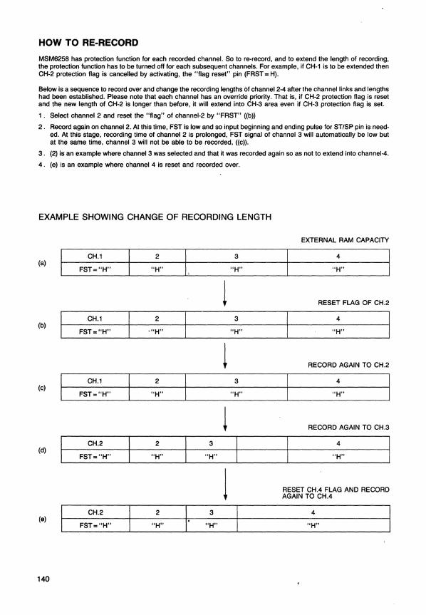
HOW TO RE-RECORD
MSM6258 has protection function for each recorded channel. So to re-record, and to extend the length of recording, the protection function has to be turned off for each subsequent channels. For example, if CH-1 is to be extended then CH-2 protection flag is cancelled by activating, the "flag reset" pin (FRST = H).
Below is a sequence to record over and change the recording lengths 6f channel 2-4 after the channel links and lengths had been established. Please note that each channel has an override priority. That is, if CH-2 protection flag is reset and the new length of CH-2 is longer than before, it will extend into CH-3 area even if CH-3 protection flag is set.
1. Select channel 2 and reset the "flag" of channel-2 by "FRST" «b»
2. Record again on channel 2. At this time, FST is low and so input beginning and ending pulse for ST/SP pin is needed. At this stage, recording time of channel 2 is prolonged, FST signal of channel 3 will automatically be low but at the same time, channel 3 will not be able to be recorded, «c».
3. (2) is an example where channel 3 was selected and that it was recorded again so as not to extend into channel-4.
4. (e) is an example where channel 4 is reset and recorded over.
EXAMPLE SHOWING CHANGE OF RECORDING LENGTH
EXTERNAL RAM CAPACITY
CH.1 2
I, 3 4
(a) FST="H" "H" "H" "H"
l RESET FLAG OF CH.2
CH.1 2 3 4 (b)
FST="H" -"H" "H" "H"
l RECORD AGAIN TO CH.2
CH.1 2 3 4 (c)
FST="H" "H" °H" "H"
~ RECORD AGAIN TO CH.3
CH.2 2 3 4 (d)
FST="H" "H" "H" "H"
j RESET CH.4 FLAG AND RECORD AGAIN TO CH.4
CH.2 2
I· 3 4
(e) FST="H" "H" "H" "H"
140
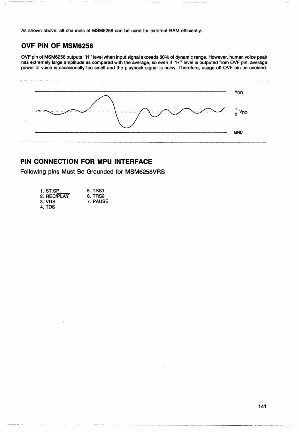
As shown above, all channels of MSM6258 can be used for external RAM efficiently.
OVF PIN OF MSM6258
OVF pin of MSM6258 outputs "H" level when input signal exceeds 80% of dynamic range. However, human voice peak has extremely large amplitude as compared with the average, so even if "H" level is outputed from OVF pin, average power of voice is occasionally too small and the playback signal is noisy. Therefore, usage off OVF pin be avoided.
PIN CONNECTION FOR MPU INTERFACE
Following pins Must Be Grounded for MSM6258VRS
1. ST.SP 5. TRS1 2. RECIPLAY 6. TRS2 3. VDS 7. PAUSE 4. TOS
Vee
GND
141
-- --- ---~-~~--.---~-----".-~~-
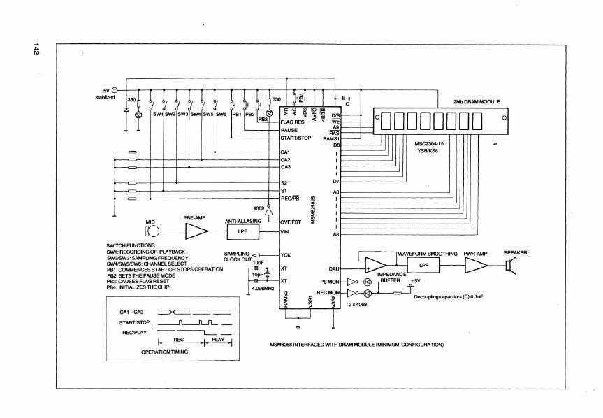
it
2Mb DRAM MODULE
L-----f----I!START/STOP
E 11111 I liE ~ I t I II~~
MIC PRE-AMP OVF/FST
+---= ! REC/PB i ~
VIN
SWITCH FUNCTIONS
r---------r---1°D D DOD D D D
D7~--------------
MSC2304-15 YSBlKSB
~.~~ M~===------------------
SWI: RECORDING OR PLAYBACK SAMPLING YCK PWR-AMP SW2ISW3' SAMPLING FREQUENCY CLOCK OUT SW4/SW5ISW6: CHANNEL SELECT IOpF PBI' COMMENCES START OR STOPS OPERATION F XT DAU PB2: SETS THE PAUSE MODE IOpF= _ PB3: CAUSES FLAG RESET XT PB MON PB4: INITIALIZES THE CHIP 4.096MHz
REC M3N Decoupllng capaCItors (C) 0 I uF
CAl -CA3
START/STOP
~-----~----
---IL-.JL.IL _
REC/PLAY --~_
/. REC '1_ PLAY ~I
OPERATION TIMING
en
L..:r---..:r--,gi;...J 2 x 4069
MSM6258 INTERFACED WITH DRAM MODULE (MINIMUM CONFIGURATION)
1 1
SPEAKER
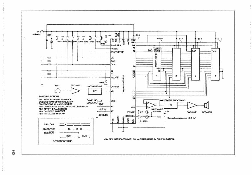
.j>. eN
L-------t--lSTART/STOP
~ 111111 II~: AO
~ rh
07 06 05 04 S I j • I I~c/PB
MIC PRE·AMP OVF/FST
LPF VIN
SWITCH FUNCTIONS
SWl RECORDING OR PLAYBACK SAMPLING SW2ISW3' SAMPLING FREQUENCY CLOCK Ou,.·<::f---IVCK
I D3.~~~~ 02 01 DO
SW4/SW5/SW6 CHANNEL SELECT 10pF
PWR·AMP
'"
PB2 SETS THE PAUSE MODE 10pF = PB3. CAUSES FLAG RESET XT PB4 INITIALIZES THE CHIP 4096MHz
~ _ Decouphng capacitors (C) 0 1 uF
1 qJ l ,,-00
~
PB1' COMMENCES START,OR STOPS OPERATION F. XT
~ CA1·CA3
START/STOP
REC/PLAY
----....-------- ------------------ ---~-
L--_ I, REC ,I, PLAY 1
OPERATION TIMING MSM 6258 INTERFACED WITH 64K x 4 DRAM (MINIMUM CONFIGURATION)
-
SPEAKER
H C
4 A
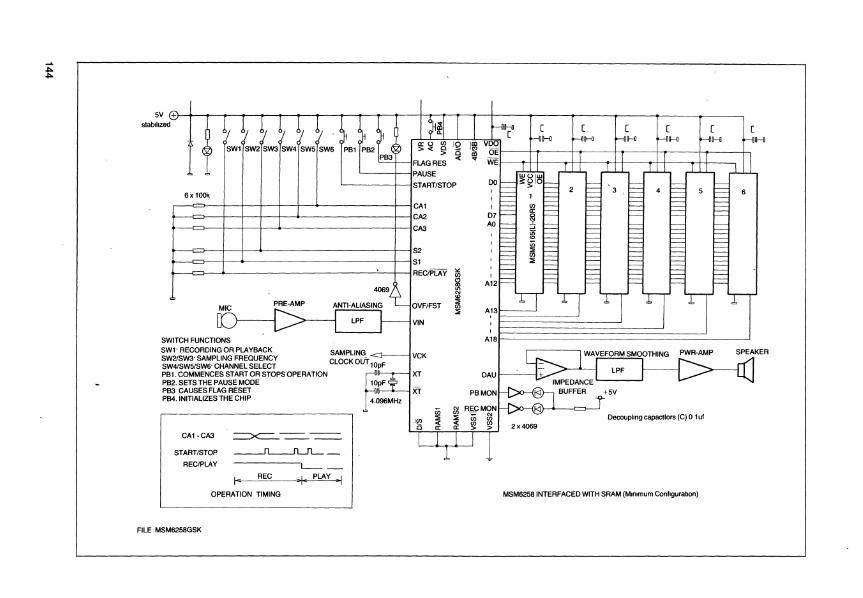
t
SWll sW21sW31sW41 swsl SW6
PAUSE
START/STOP
6x lOOk
CAl
CA2
CA3
S2
SI
REC/PLAY " (/)
C!J ., 4069/\ "' '" "'
OVF/FST ::; (/) ::;
VIN
SWITCH FUNCTIONS
~~~;~i~~~~~~::~6~~~~y SAMPLING <CJ-------I VCK SW4/SWS/SW6' CHANNEL SELECT CLOCK OUT 1 OpF PB1. COMMENCES START OR STOPS OPERATION PB2. SETS THE PAUSE MODE PB3 CAUSES FLAG RESET PB4.INITIALIZES THE CHIP
CA1-CA3
START/STOP
REC/PLAY
------...------ ------------ -- ---~-
L-_
I~ REC 'I, PLAY _I OPERATION TIMING
FILE MSM6258GSK
GPF c5
F~MHZ
XT
XT
Al~~1 ~~~-DAU f------l
Decouphng capactlors (C) 0 1 uf 2x4069
MSM62S81NTERFACED WITH SRAM (MInimum Conflgurallon)
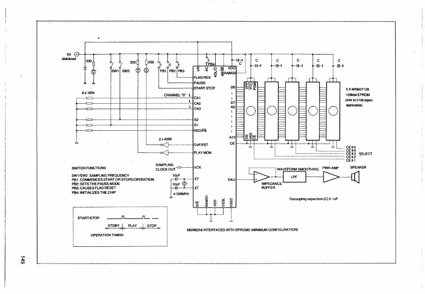
..... ~
5V (+! , , stabilized
330 330 330
SW11 S~2
6x 100k
SWITCH FUNCTIONS
SWlISW2. SAMPLING FREQUENCY PB1. COMMENCES START OR STOPSIOPERATION PB2: SETS THE PAUSE MODE PB3: CAUSES FLAG RESET PB4: INITIALIZES THE CHip
PAUSE
START STOP
CHANNEL "0" L I CA1
CA2 L 'CA3
2 x 4069
SAMPLING CLOCK OUT
p.10~
10pF c:::::J
4~6MHZ
I
S2
S1
REC/PB
OVF/FST
PLAYMON
VCK
XT
lIT
START/STOP ~-
DAU
5XMSM27128
128kbitEPROM
(64k to 512k types
applicable)
CE#5 L ______ ~======~======~~~~~~~CE#4 CE#3 SELECT
CE#2 CE#1
Decouphng capacitors (C) 0 1 uF
MSM6258 INTERFACED WITH EPROMS (MINIMUM CONFIGURATION)
OPERATION TIMING
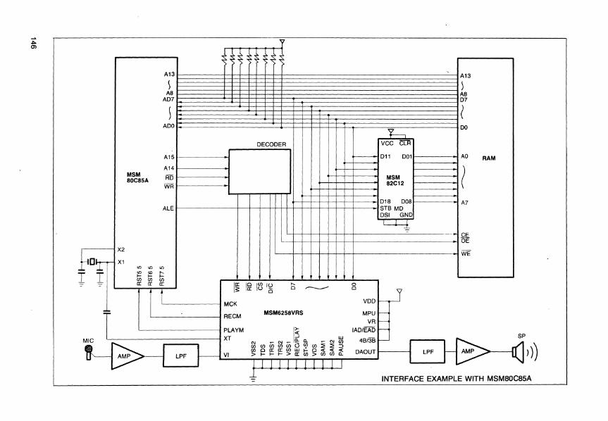
-"
~ 'V
. ~ : ~ ~ : ~
A13 ,
A13
~ ~ A8 A8
AD7 D7
~ ( ADO DO
~ DECODER VCC ern
A15 t------- Dll DOl AD RAM
A14 ( MSM AD MSM 80C85A WR 82C12
D18 D08 A7 ALE STB MD
DSI GND .~
--~ CE
OE
.0o~ X2
-. WE X1
L() L() L()
L() to "-I I f- f- f-(fJ (fJ (fJ a: cr a:
I~ 10 1(fJ IU "- 0
1 a: U (3 0 -------- 0
MCK VDD f--
"" T RECM MSM6258VRS MPU f--
VR f--
PLAYM I~ IAD/EAD f--<C XT ...J w
4B/38 - 1-l?>-<f) )) C\l ...-N...-Q::a.. ,....N(J)
~~{ ~VI (fJ(fJ(fJ(fJ(fJUC(>(fJ::;::;:;' r (fJoa:a:(fJWf-O<C<C<C DAOUT LPF
LPF >f-f-f->a:(fJ>(fJ(fJa. I I I I I I I I I I I ~ INTERFACE EXAMPLE WITH MSM80C85A
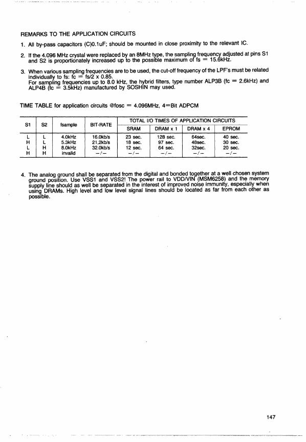
REMARKS TO THE APPLICATION CIRCUITS
1. All by-pass capacitors (C)0.1 uF; should be mounted in close proximity to the relevant IC.
2. If the 4.096 MHz crystal were replaced by an SMHz type, the sampling frequency adjusted at pins S1 and S2 is proportionately increased up to the possible maximum of fs = 15.6kHz.
3. When various sampling frequencies are to be used, the cut-off frequency of the LPF's must be related individually to fs: fc = fs/2 x 0.S5. For sampling frequencies up to S.O kHz, the hybrid filters, type number ALP3B (fc = 2.6kHz) and ALP4B (fc = 3.5kHz) manufactured by SOSHIN may used.
TIME TABLE for application circuits @fosc = 4.096MHz, 4=Bit ADPCM
TOTAL I/O TIMES OF APPLICATION CIRCUITS S1 S2 fsample BIT-RATE
SRAM DRAM x 1 DRAM x 4 EPROM
L L 4.0kHz 16.0kb/s 23 sec. 128 sec. 64sec. 40 sec. H L 5.3kHz 21,2kb/s 18 sec. 97 sec. 48sec. 30 sec. L H 8.0kHz 32.0kb/s 12 sec. 64 sec. 32sec. 20 sec. H H invalid -/- -/- -/- -/- -/-
4. The analog ground shall be separated from the digital and bonded together at a well chosen system ground position. Use VSS1 and VSS2! The power rail to VDDNIN (MSM625S) and the memory supply line should as well be separated in the interest of improved noise immunity, especially when usinQ DRAMs. High level and low level signal lines should be located as far from each other as possible.
147
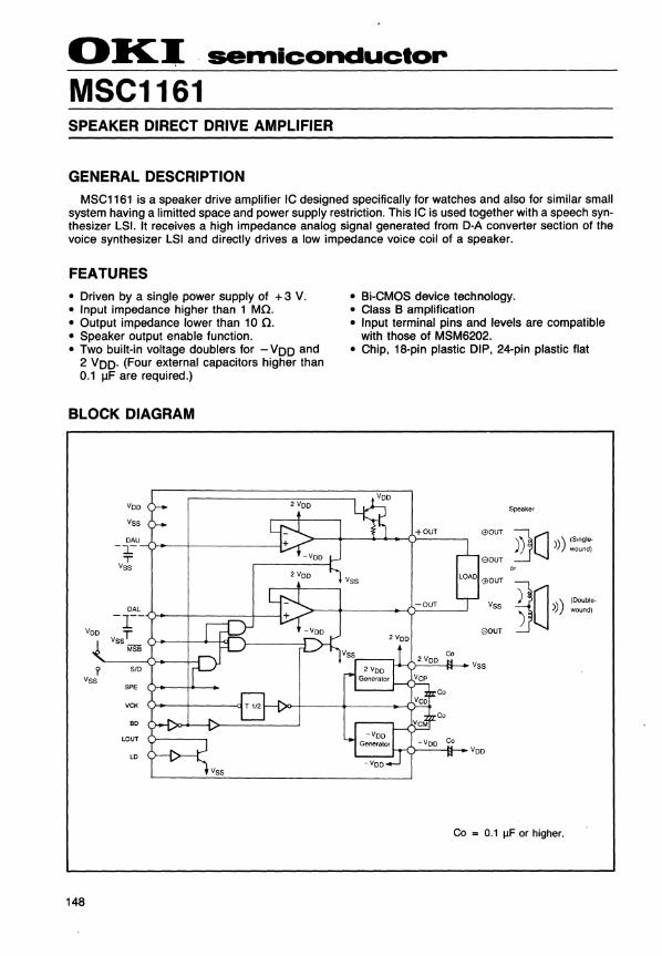
OKI semiconductor
MSC1161 SPEAKER DIRECT DRIVE AMPLIFIER
GENERAL DESCRIPTION
MSC1161 is a speaker drive amplifier IC designed specifically for watches and also for similar small system having a limitted space and power supply restriction. This IC is used together with a speech synthesizer LSI. It receives a high impedance analog signal generated from D-A converter section of the voice synthesizer LSI and directly drives a low impedance voice coil of a speaker.
FEATURES
• Driven by a single power supply of + 3 V. • Input impedance higher than 1 MO. • Output impedance lower than 10 O. • Speaker output enable function. • Two built-in voltage doublers for - VDD and
2 VDD. (Four external capacitors higher than 0.1 IlF are required.)
BLOCK DIAGRAM
Voo
VSS
oAU -T
T VSS
oAL
Voo
-r-vssT
MSB
? SID
VSS SPE
VCK
BO
LOUT
LD
148
• Bi-CMOS device technology. • Class B amplification • Input terminal pins and levels are compatible
with those of MSM6202. • Chip, 18-pin plastic DIP, 24-pin plastic flat
Speaker
$OUT
~(] »)) ~~:~~; eOUT
~O»)) VSS (Double-
wound)
eOUT
VSS
VDo
Co = 0.1 IlF or higher.
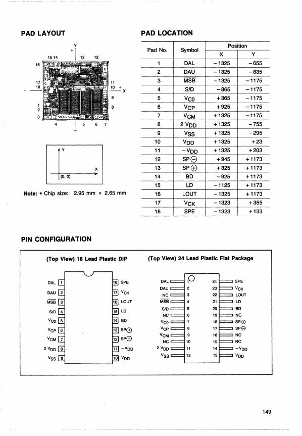
PAD LAYOUT
y
16
4 567
11 10 + --x 9
8
Note: • Chip size: 2.95 mm x 2.65 mm
PIN CONFIGURATION
(Top View) 18 Lead Plastic DIP
SPE
VCK
LOUT
LO
BO
Spe
Spe
-VOO
VOO
PAD LOCATION
Pad No. Symbol Position
X y
1 DAL -1325 -655
2 DAU -1325 -835
3 MSB -1325 -1175
4 SID -865 -1175
5 Veo +365 -1175
6 VCP +925 -1175
7 VCM +1325 -1175
8 2VDD +1325 -755
9 VSS +1325 -295
10 VDD +1325 +23
11 -VDD +1325 +203
12 sp8 +945 + 1173
13 SPc±) +325 +1173
14 BD -925 + 1173
15 LD -1125 + 1173
16 LOUT -1325 +1173
17 VCK -1323 +355
18 SPE -1323 +133
(Top View) 24 Lead Plastic Flat Package
OAL 10 SPE OAU 2 VCK
NC 3 LOUT MSB 4 LO
SID 5 BO NC 6 NC
Vco 7 spe Vcp 8 spG
VCM 9 NC NC NC
2VOO -VOO Vss Voo
149
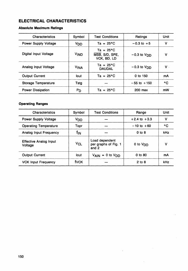
ELECTRICAL CHARACTERISTICS
Absolute Maximum Ratings
Characteristics Symbol Test Conditions Ratings Unit
Power Supply Voltage VDD Ta = 25°C -0.3 to +5 V
Ta = 25°C Digital Input Voltage VIND MSB, SID, SPE, -0.3 to VDD V
VCK, BD, lD
Analog Input Voltage VINA Ta = 25°C -0.3 to VDD V· DAUDAl
Output Current lout Ta = 25°C o to 150 mA
Storage Temperature Tstg - -55 to + 150 °C
Power Dissipation Po Ta = 25°C 200 max mW
Operating Ranges
Characteristics Symbol Test Conditions Range Unit
Power Supply Voltage VDD - +2.4 to +3.3 V
Operating Temperature Topr - -10 to +60 °C
Analog Input Frequency fiN - o to 8 kHz
Effective Analog Input VCl
load dependent Voltage per graphs of Fig. 1 o to VDD V
and 2
Output Current lout VAIN = 0 to VDD o to 80 mA
VCK Input Frequency fVCK - 2 to 8 kHz
150
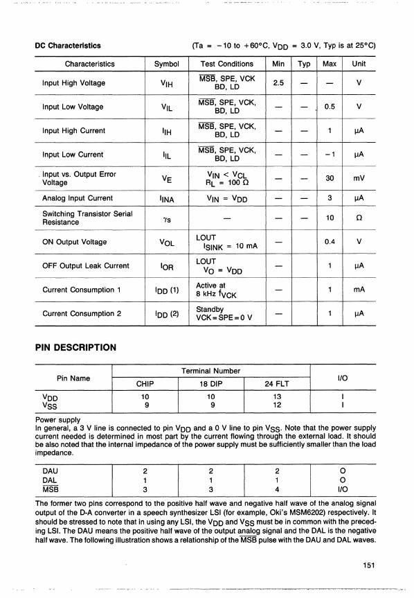
DC Characteristics (Ta = -10 to +60°C, VOO = 3.0 V, Typ is at 25°C)
Characteristics Symbol Test Conditions Min Typ Max Unit
Input High Voltage VIH MSB,SPE, VCK 2.5 - - V BO, LO
Input Low Voltage VIL MSB, SPE, VCK, - - 0.5 V BO, LO
Input High Current IIH MSB, SPE, VCK, - - 1 IlA BO, LO
Input Low Current IlL MSB, SPE, VCK, - - -1 IlA BO, LO
. Input vs. Output Error VE VIN < VCL - - 30 mV
Voltage RL = 100 n
Analog Input Current IINA VIN = VOO - - 3 IlA
Switching Transistor Serial 'Ys - - - 10 n Resistance
ON Output Voltage VOL LOUT 0.4 V
ISINK = 10 mA -
OFF Output Leak Current lOR LOUT 1 IlA
Vo = VOO -
Current Consumption 1 100 (1) Active at 1 mA 8 kHz fVCK
-
Current Consumption 2 100 (2) Standby - 1 IlA VCK=SPE=O V
PIN DESCRIPTION
Terminal Number Pin Name
CHIP 18 DIP 24 FLT I/O
VOO 10 10 13 I VSS 9 9 12 I
Power supply In general, a 3 V line is connected to pin VOO and a 0 V line to pin VSS. Note that the power supply current needed is determined in most part by the current flowing through the external load. It should be also noted that the internal impedance of the power supply must be sufficiently smaller than the load impedance.
OAU OAL MSB
2 1 3
2
3
2 1 4
o o I/O
The former two pins correspond to the positive half wave and negative half wave of the analog signal output of the O-A converter in a speech synthesizer LSI (for example, Oki's MSM6202) respectively. It should be stressed to note that in using any LSI, the VOO and VSS must be in common with the preceding LSI. The OAU means the positive half wave of the output analog signal and the OAL is the negative half wave. The following illustration shows a relationship of the MSB pulse with the OAU and OAL waves.
151
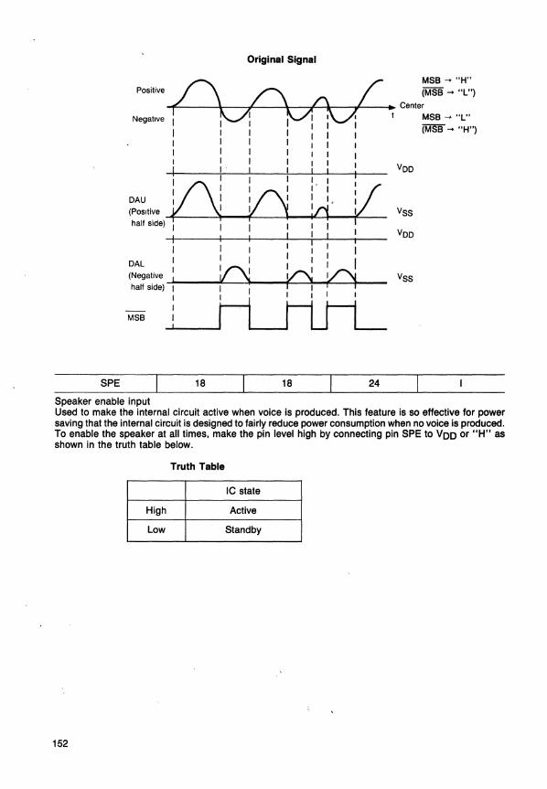
Original Signal
Positive ~ /\ /
Negatlve~'\ ~ ~ I I I I ;'-'i I I I I I I I I I I I I I I I I I I I I I I I I I ul :I~I:
DAU I I I I
(Positive ~ I
half side) I I I I I I
I I I I: I I
1/ i
DAL
MSB
SPE 18 18 24
Speaker enable input
MSB -+ "H"
(MSB -+ "L")
Center
VDD
VSS
VDD
VSS
MSB -+ "L" (MSB -+ "H")
Used to make the internal circuit active when voice is produced. This feature is so effective for power saving that the internal circuit is designed to fairly reduce power consumption when no voice is produced. To enable the speaker at all times, make the pin level high by connecting pin SPE to VOO or "H" as shown in the truth table below.
Truth Table
Ie state
High Active
Low Standby
152
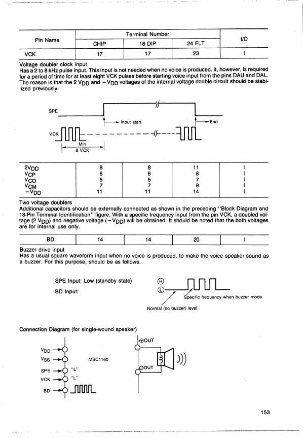
Terminal Number Pin Name 110
CHIP 18 DIP 24 FLT
VCK 17 17 23 I
Voltage doubler clock input Has a 2 to 8 kHz pulse input. This input is not needed when no voice is produced. It, however, is required for a period of time for at least eight VCK pulses before starting voice input from the pins DAU and DAL. The reason is that the 2 VDD and - VDD voltages of the internal voltage double circuit should be stabilized previously.
~ _ ~f I SPE
______ ...1 Input startt \---~ -E-nd-
VC~-- - --- - ---ff----iJlJL
I" 8 ~~K ~ I
2VDD 8 8 11 I VCP 6 6 8 I VCO 5 5 7 I VCM 7 7 9 I -VDD 11 11 14 I
Two voltage doublers Additional capacitors should be externally connected as shown in the preceding "Block Diagram and 18-Pin Terminal Identification" figure. With a specific frequency input from the pin VCK, a doubled voltage (2 VDD) and negative voltage (- VDD) will be obtained. It should be noted that the both voltages are for internal use only.
BD 14 14 20
Buzzer drive input Has a usual square waveform input when no voice is produced, to make the voice speaker sound as a buzzer. For this purpose, should be as follows.
SPE Input: Low (standby state)
BD Input:
Connection Diagram (for Single-wound speaker)
"L"
"L"
MSC1160
JU1JlIL
® nnn ©---.-J/U U L-
/ Specific frequency when buzzer mode
Normal (no buzzer) level
153
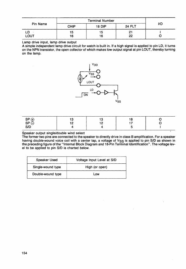
Terminal Number Pin Name
CHIP 18 DIP 24 FLT 1/0
LD 15 15 21 I LOUT 16 16 22 0
Lamp drive input, lamp drive output A simple independent lamp drive circuit for watch is built in. If a high signal is applied to pin LD, it turns on the NPN transistor, the open collector of which makes low output signal at pin LOUT, thereby turning on the lamp.
SP (f) SP8 SID
13 12 4
Speaker output singleldouble wind select
13 12
4
vss
18 17 5
o o I
The former two pins are connected to the speaker to directly drive in class B amplification. For a speaker having double-wound voice coil with a center tap, a voltage of VSS is applied to pin SID as shown in the preceding figure of the" Internal Block Diagram and 18-Pin Terminal Identification" . The voltage level to be applied to pin SID is charted below.
Speaker Used Voltage Input Level at SID
Single-wound type High (or open)
Double-wound type Low
154
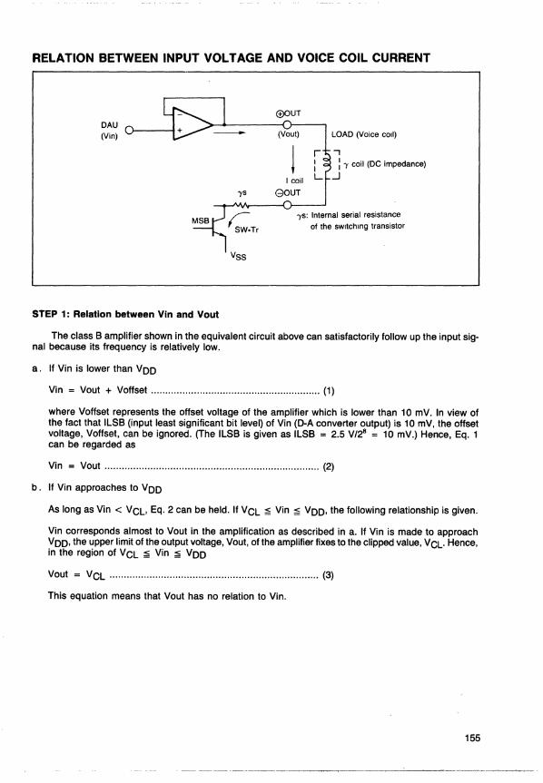
RELATION BETWEEN INPUT VOLT AGE AND VOICE COIL CURRENT
DAU (Vin)
STEP 1: Relation between Vin and Vout
)'5
C SW.Tr
VSS
EElOUT
(Vout)
I coil
gOUT
LOAD (Voice cOil)
r .., : : )' coil (DC impedance)
L ...J
)'5: Internal serial resistance of the sWitching transistor
The class B amplifier shown in the equivalent circuit above can satisfactorily follow up the input signal because its frequency is relatively low.
a. If Vin is lower than VOO
Vin = Vout + Voffset ........................................................... (1)
where Voffset represents the offset voltage of the amplifier which is lower than 10 mV. In view of the fact that IlSB (input least significant bit level) of Vin (D-A converter output) is 10 mV, the offset voltage, Voffset, can be ignored. (The IlSB is given as IlSB = 2.5 V/28 = 10 mV.) Hence, Eq. 1 can be regarded as
Vin = Vout ........................................................................... (2)
b. If Vin approaches to VOO
As long as Vin < Vel, Eq. 2 can be held. If Vel ~ Vin ~ VOO, the following relationship is given.
Vin corresponds almost to Vout in the amplification as described in a. If Vin is made to approach VOO, the upper limit of the output voltage, Vout, of the amplifier fixes to the clipped value, Vel. Hence, in the region of Vel ~ Vin ~ VOO
Vout = Vel ......................................................................... (3)
This equation means that Vout has no relation to Vin.
155
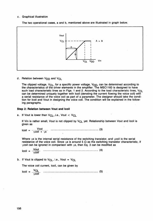
c. Graphical illustration
The two operational cases, a and b, mentioned above are illustrated in graph below.
Vou!
VCl A = B
VCl Voo Vin
d. Relation between VOO and VCl
The clipped voltage, VCl, for a specific power voltage, VOO, can be determined according to the characteristics of the driver elements in the amplifier. The MSC1160 is designed to have such load characte~istic lines as in Figs. 1 and 2. According to the load characteristic lines, VCl can be determined uniquely together with Icoil (denoting the current flowing the voice coil) with a serial resistance of the voice coil as part of a parameter. The designer should take the condition for Icoil and Vout in designing the voice coil. The condition will be explained in the following paragraphs.
Step 2: Relation between Vout and Icoil
a. If Vout is lower than VCl,J.e., Vout < VCl
If Vin is rather small, Vout is not clipped by VCl yet. Relationship between Vout and Icoil is given as
Icoil = 'Yco~o~t 'Ys ........................................................... (3)
Where 'Ys is the internal serial resistance of the switching transistor, and 'Ycoil is the serial resistance of the voice coil. Since 'Ys is around 5 n as the switching transistor characteristic, if 'Ycoil can be ignored in comparison with 'Ys, then Eq. 3 can be modified as
Icoil = vou.t .................................................................... (4) 'Ycoll
b. If Vout is clipped to VCl, i.e., Vout = VCl
The voice coil current, Icoil, can be given by
Icoil - VCl .................................................................... (5) - 'Ycoil
156
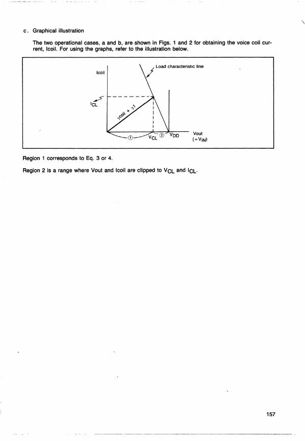
c. Graphical illustration
The two operational cases, a and b, are shown in Figs. 1 and 2 for obtaining the voice coil current, Icoil. For using the graphs, refer to the illustration below.
tcoil
Region 1 corresponds to Eq. 3 or 4.
Vout (=VtN)
Region 2 is a range where Vout and Icoil are clipped to VCl and ICl.
157
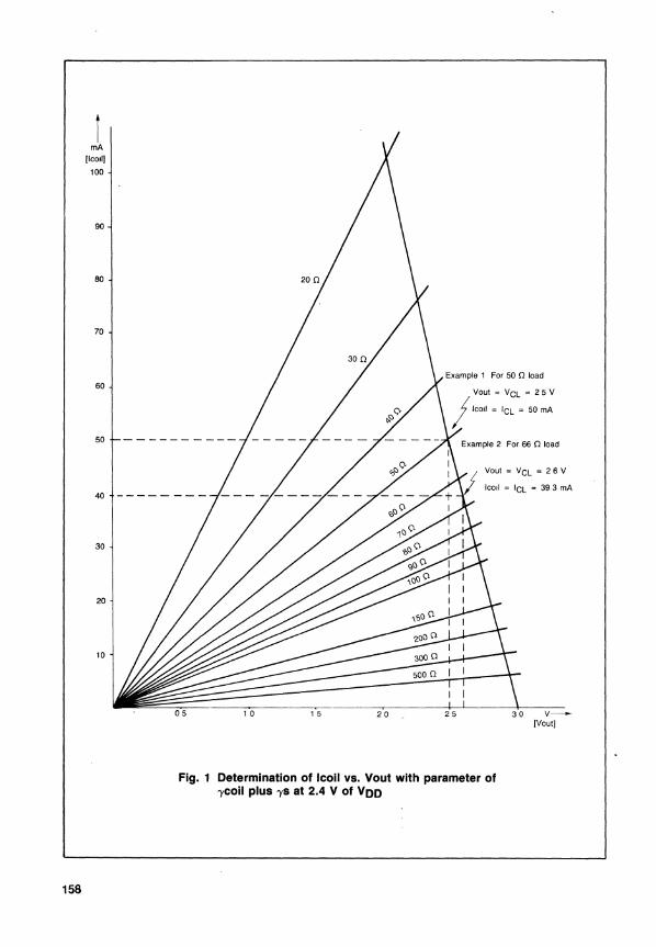
158
t rnA
[lcoll[
100
90
80
70
60
50
Example 1 For 50 n load
Vout = VCl = 25V
Icoll = ICl = 50 mA
Example 2 For 66 n load
40 --------
Vout = V Cl = 2 6 V
Icoll = ICl = 39 3 rnA
30
20
10
10 15 20
Fig. 1 Determination of Icoil vs. Vout with parameter of 'Ycoil plus 'Ys at 2.4 V of VDD
V~
[Vout]
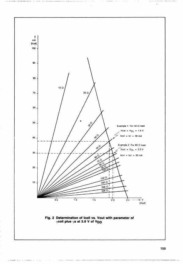
t mA
[leo,II)
100
90
80
70
60
50
40
30
20
10
10 15
Example 1 For 50 0 load
Vout = VCL = 1 9 V
leoll = lei = 38 mA
Example 2 For 66 0 load
VOU! = VCL = 20V
Icoll = Icc = 30 mA
4 ~-_V
[Vaut]
Fig. 2 Determination of Icoil vs. Vout with parameter of 'Ycoil plus 'Ys at 3.0 V of VDD
159

APPENDIX

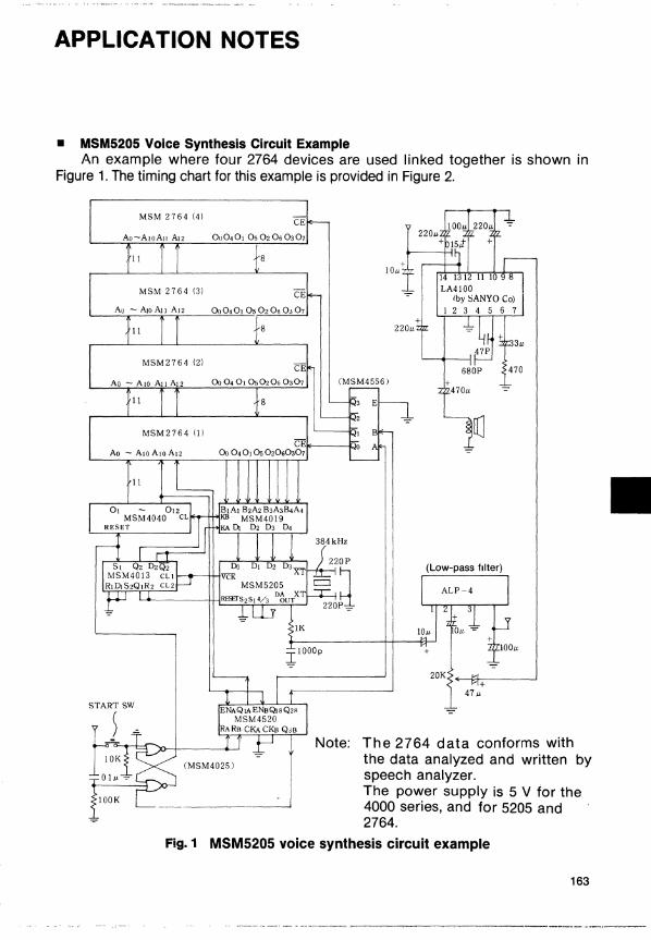
APPLICATION NOTES
• MSM5205 Voice Synthesis Circuit Example An example where four 2764 devices are used linked together is shown in
Figure 1. The timing chart for this example is provided in Figure 2.
(MSM4025)
100" 220" -::-
L-....... _1 47P
680P 470 (MSM4556) +
470"
20K< .. --l:'>------' +
47 "
Note: The 2764 data conforms with the data analyzed and written by speech analyzer. The power supply is 5 V for the 4000 series, and for 5205 and 2764.
Fig. 1 MSM5205 voice synthesis circuit example
163
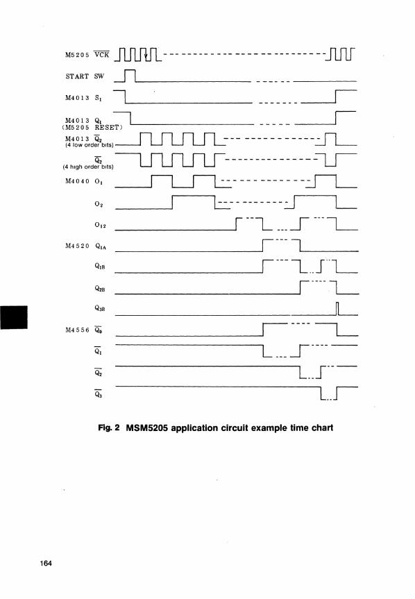
M5 205 VCK JlJ1.J1J"L ---------------------------llflf START SW -.JlL--____________________ _ M4013 SI 1 .... __________ _ -------~ M4013 QI I
(M5205 RESET) '------------------ ----- __ --'I M401 3 ~ n n n n - -_______ - _____ n (4 low order bits) --l LJ LJ LJ L -.-.J L-
(4hlghOrd!fzbltS)~--------------~ M4040 0 1 -------------~
02 L-- -------.:r--L 012 r--L ___ S---~
M4520 Q1A i---l Q1B i---L .. J'··L Q2B I----·~
Q3B L M4556 Q;; ,----1.-
QI L ___ S-----Q2 L __ S---Q3 L_r
Fig. 2 MSM5205 application circuit example time chart
164
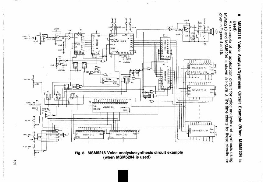
... Ol (11
~AM SEL A
RAM SEL ! B •
IUOK Fig,3 MSM5218 Voice analysis/synthesis circuit example (when MSM5204 is used)
eg_s: • < (f)
~~»cs:: S- '" ::J Xl (f) 11 ..... (Oc.s:: -- CD X _ U1 CO OlOl I\)
~::J3 .... 5l 0."2. <XI ~s:(O < 0lg20 2. ::J;:,.- (") 0. (J1 Ol (I)
(J1 '" ::J -0 ~Ol __ "0 en "0 en -:::T(") 00l :Ett ::JO
::J S-(") 11""' --(") COc C --.... -(0_
w O - ""' --1< :::TO CD 0-ttCD 30l CD::J (")~ :::T'< Olen .... --c;ren _Ol 0::J .... 0. -en :::T,< 5l::J CD-:::T (")(0 ~.(J)
(") -cen ;::t:c en en Ol SCOCO
l> :::l II)
i ~ (f) '< :::l -:::T (I) en iii'
o ~' c ::;:
m ~ 3 'tJ c;"
i :::T (I) :::l
s:: (f)
s:: U1 I\)
g iii'
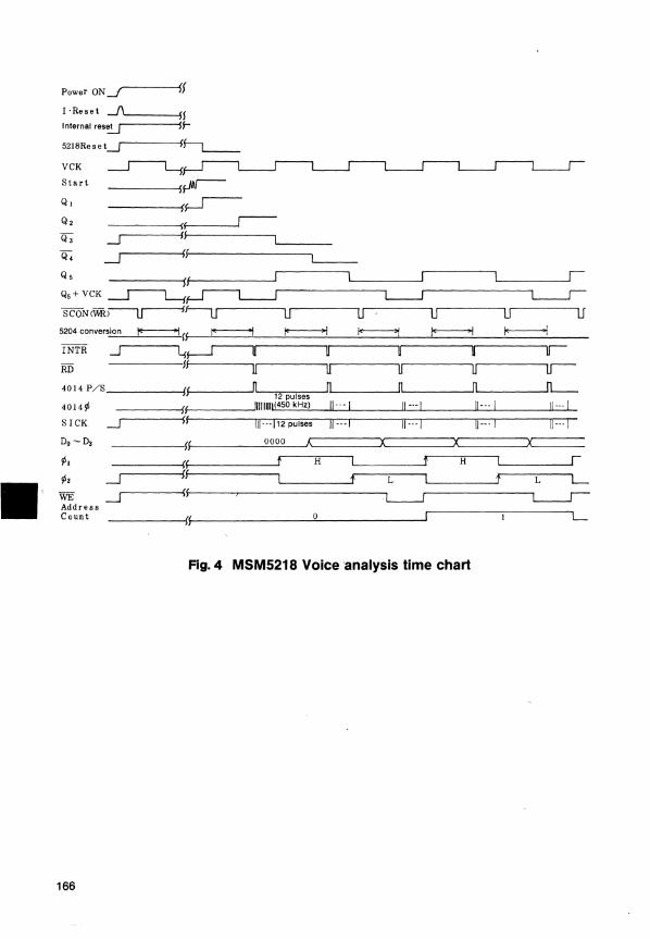
Power ON Jr---~ff
I . Re set -1'Il..-----JH Internal res~ $I ....
5218Re set --1r -----i
VCK
Start
Q,
Q2
Q,
Q;
Q5
166
....J .....J
u u U-
il U u U U--~ __ ~nl..~~~~n,~ __ ~~ ___ ~n.~ ____ ~
12 pulses ____ --ff-____ "I1UII'(450kHZ) 11---1 11-·-1 11---1 11_ 00 1
111---112 pulses 11 000 1 11 00 .1 liml 11- 00 1
~ ____ O~O~O~O~A~ ___ ~Xl.. ___ ~XL ___ ~XL __ _
H t H L-___ ---Ir t L t L L
r----~S~---,---------------~.~~-----------~
L
Fig.4 MSM5218 Voice analysis time chart
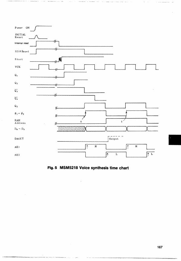
Power ON ~
INITIAL 1\ Reset ---.J '---
~h,--____________ _ Internal reset --.J 1_ r----~{'rf--------~
5218Reset ~
Start
VCK
Q,
-------iff---~
---~~~------------~~
ll-f ___ --'I 1 I L---I _ ¢, = ¢,
RAM Address
Do - Da
DAOUT
AEI
AE2
,, _____ ~t~--~I t~--~~ ff- / "--------t+
If 0 I 17 ~
fJl//!I////lIJlIlJA'--_--'X'--_X'-------'~ r-----:Output
----_____ ~I
_______ --'1 i H ~_~'i H L I It '----------' 1-1 __ --'ffL L
Fig.5 MSM5218 Voice synthesis time chart
167
• MSM5218 Voice Analysis/Synthesis Circuit Example (When 12-bit AD Converter is Used) . An example of an application circuit for voice analysis and synthesis using
MSM5218 and a 12-bit AD converter (ADC-80AG is manufactured by *MN Co.) is shown in Figure 6.
The time charts for these circuits are given in Figures 5 and 7.
* Micro Network Corp.
168
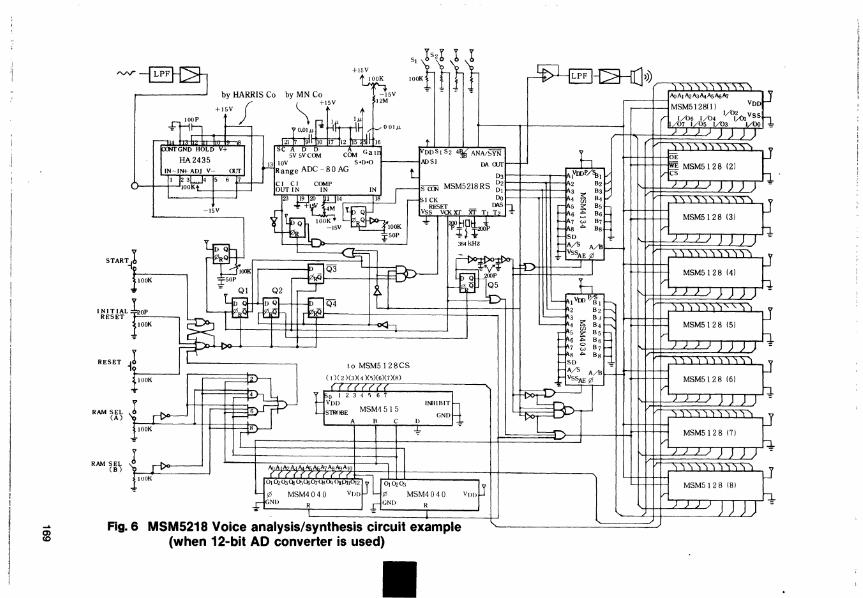
..... m
~5V jl~
~~ I
+15V ,:t;h~t ~~)j)( '1 '1'i'i'i'i 'i'i'i'" 'I
~AoAlAeA3"'AsAoAo MSM5128111 Voo
I/06 I/04 V~~I VSS
~I/03 I/jl:: J J J
t
6 7 w 8 ....
SO
1 Voo e:;r11 2 B2 INITIAL 3 B3 RESET 4 a: B4
5 ~ B5 6 ~ B6 7 CJJ B7 8 ..". B8
SO _ RESET i! to MSM5 12 8CS A/S A/ll -
It --. (1)(2 )(3)(4 )(5)(6)(7)(8) VSSAE ¢ i lOOK
(1)(2)(3)(L '
T77
RAMSEL~ (A)
lOOK
~
RAM SEL .1 (B)
~ ~
o I 2 3 4 'j 6 7 VOO
SlROBE MSM4515 INHIBIT
GND I A C f) ,.~
I I {" -
AIlA1A?AiAtm~/v,!:.AiO
Ws MSM5128 121 CS
)))n2) ISS:SSSSSS:i~
~ MSM5128 131
)))11]) 1~5JSJ5::ill
~ MSM5128 141
LJ)))) ~
[lOOK 0] ()2(}JQj O:JQjOr{~,Oj OlP1l0 12
¢ MSM4 040 VIm
.N"
OJ ()20:1
¢ MSM4040 J" ~~ fll I .""" 1 ",,' II ]Jj Fig.6 MSM5218 Voice analysis/synthesis circuit example
(when 12-bit AD converter is used)
J ) J J
-=
-
-
-
-
-
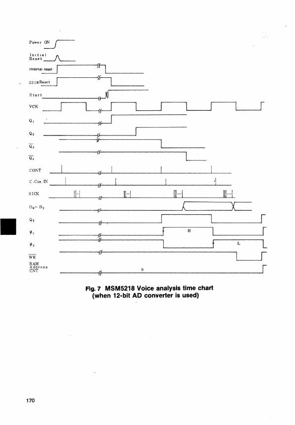
Power~
InitIal A Reset---1 ~
'---_r
111---1 111---1
~ ___ ---Jr ____________ ~-----H----~ I
L L L..-----II
------1r-----~----------------~1
170
Fig.7 MSM5218 Voice analysis time chart (when 12-bit AD converter is used)
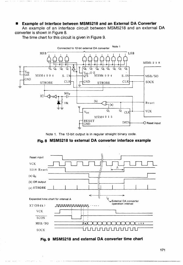
• Example of Interface between MSM5218 and an External DA Converter An example of an interface circuit between MSM5218 and an external DA
converter is shown in Figure 8. The time chart for this circuit is given in Figure 9.
Connected to 12-bit external DA converter Note 1
MSBr,----------------~------------------LSB
MSM5 2 1 8
VDD
O.E MSM4094 S. INI-------l MSB/SO GND
STROBE CLK SOCK ~----~~~------~
(c) '-".h....,../L~-.J 1-_+ ____________ ----,
Q3
MSM4 0 1 5 RESET
Q, CL·~>---~ VCK
GND DATN-----< Reset input
Note 1. The 12-bit output is in regular straight binary code.
Fig.8 MSM5218 to external DA converter interface example
Reset lnput
VCK
5218 Reset
(a) Q3 ------~====~~r----~
(b) OR output
(c) S TRO BE ----'-____ -'--__ --' ____ ---'-___ If.L-____ L-__ --L ____ ....L ____ .J-_
Expanded time chart for lnterval A ~External DA converter operation interval
XT (3 8 4 k)
VCK
SCON
MSB/SO
SOCK
-.-J : ,: ~:~ ____________ ~==============:: --------,LJ-: :
~-----I I I '
------------, , ____________ ~L~S~B __ __
Fig.9 MSM5218 and external DA converter time chart
171
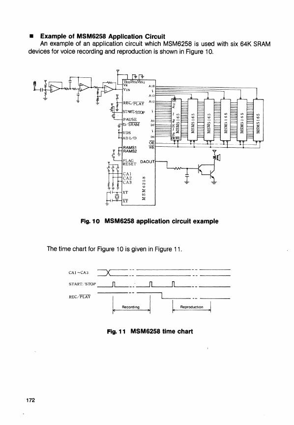
• Example of MSM6258 Application Circuit An example of an application circuit which MSM6258 is used with six 64K SRAM
devices for voice recording and reproduction is shown in Figure 10.
Fig. 10 MSM6258 application circuit example
The time chart for Figure 10 is given in Figure 11.
CAI-CA3 =:::::x== -- _______ _ START~"STOP -----It-__ -~ _____ _
REC/PLAY
~ Recording .1 ReproductIon
Fig. 11 MSM6258 time chart
172
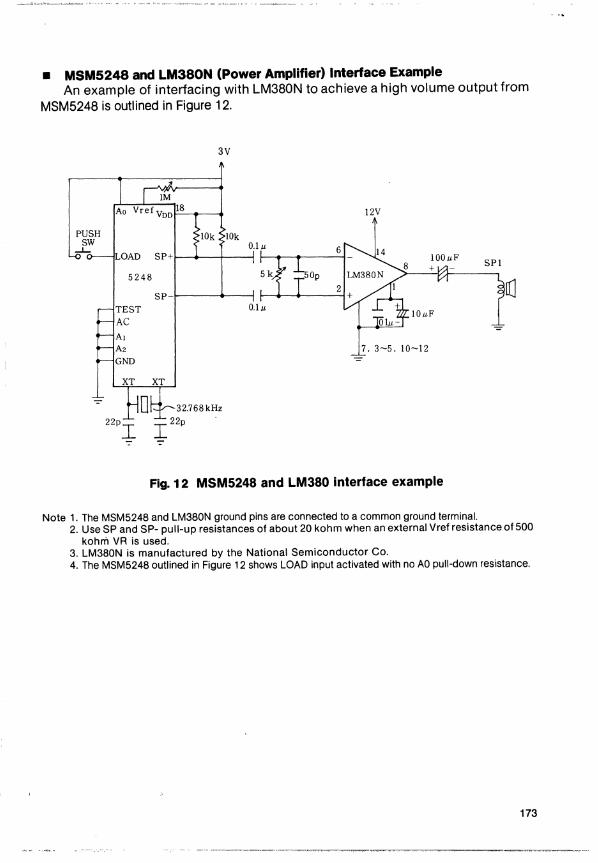
• MSM5248 and LM380N (Power Amplifier) Interface Example An example of interfacing with LM380N to achieve a high volume output from
MSM5248 is outlined in Figure 12.
3V
12V
PUSH 10k 10k sw O.lu ..J... LOAD SP+
5248
SP-TEST O.lu
AC
Al A2 7.3-5.10-12 GND
Dtl-:32.768 kHz
22PI 1 22P .
Fig. 12 MSM5248 and LM380 interface example
Note 1. The MSM5248 and LM380N ground pins are connected to a common ground terminal. 2. Use SP and SP- pull-up resistances of about 20 kohm when an external Vref resistance of 500
kohni VR is used. 3. LM380N is manufactured by the National Semiconductor Co. 4. The MSM5248 outlined in Figure 12 shows LOAD input activated with no AO pull-down resistance.
173
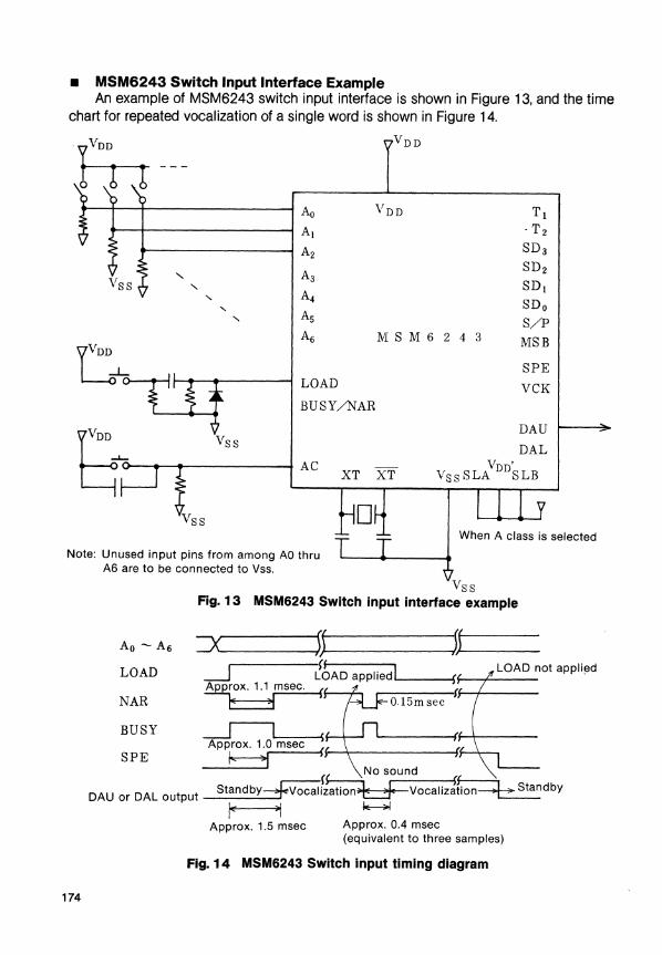
• MSM6243 Switch Input Interface Example An example of MSM6243 switch input interface is shown in Figure 13. and the time
chart for repeated vocalization of a single word is shown in Figure 14.
VDD
Ao VDD TJ
Al . T2
A2 SD 3
" A3 SD2
"- SD I "- A4
SDo '-"- A5 S/P
A6 MSM6243 MSB TVDDcr- SPE
LOAD VCK BUSY/NAR
t;~ DAU
VSS DAL AC V .
XT XT Vss SLA DDSLB
Vss When A class is selected
Note: Unused input pins from among AO thru A6 are to be connected to Vss.
174
LOAD
NAR
BUSY
SPE
Vss Fig. 13 MSM6243 Switch input interface example
=x )f "
ff T#
-.Jr-----~bAD applied Ll __ ~'~---f::...-LO_A_D_not appliild
Approx. 1.1 msec. ( r-----~rf_+------r: :J O.15msec
APJrox.1.0~I_m~se~c~{~~~ _______ ff-~~ b:=::I No sound
StandbY~f~ vocalizl~dbY IE'., ~
DAU or DAL output
Approx. 1.5 msec Approx. 0.4 msec (equivalent to three samples)
Fig. 14 MSM6243 Switch input timing diagram
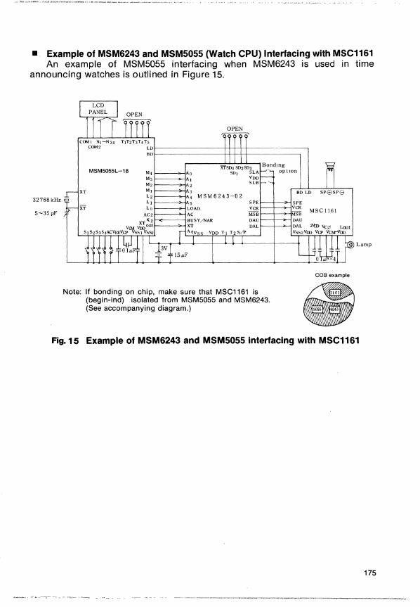
• Example of MSM6243 and MSM5055 (Watch CPU) Interfacing with MSC1161 An example of MSM5055 interfacing when MSM6243 is used in time
announcing watches is outlined in Figure 15.
MSM5055L-18
XT
OPEN
f--------t-+-f++~--- -------,
USDO SD2 SD3 BondIng SOl SLA op t IOn
VDD 5LB ~~
SO LO
32168 kHz Cl
M4f-------<>~AO M31---_-lA M21------i>--iA MII---~-lA L21---_-iA LII---_-lA Lof--->~
MSM6243-02 SPEI---+-....jSPE
5-35 pF ~~~ v~: MSC 1161 DAUI--+~~ DALI--+-~
Note: If bonding on chip, make sure that MSC1161 is (begin-ind) isolated from MSM5055 and MSM6243. (See accompanying diagram.)
COB example
~ \\SJ
Lamp
Fig.15 Example of MSM6243 and MSM5055 interfacing with MSC1161
175
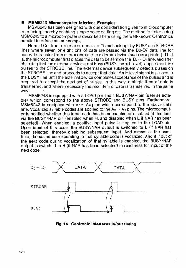
• MSM6243 Microcomputer Interface Examples MSM6243 has been designed with due consideration given to microcomputer
interfacing, thereby enabling simple voice editing etc. The method for interfacing MSM6243 to a microcomputer is described here using the well-known Centronics parallel interface as an example.
Normal Centronic interfaces consist of "handshaking" by BUSY and STROBE lines where seven or eight bits of data are passed via the 00-07 data line for accurate transfer from microcomputer to external device (such as a printer). That is, the microcomputer first places the data to be sent on the Do -- D7 line, and after checking that the external device is not busy (BUSY line at L level). applies positive pulses to the STROBE line. The external device subsequently detects pulses on the STROBE line and proceeds to accept that data. An H level signal is passed to the BUSY line until the external device completes acceptance of the pulses and is prepared to accept the next set of pulses. In this way, a single item of data is transferred, and where necessary the next item of data is transferred in the same way.
MSM6243 is equipped with a LOAD pin and a BUSY INAR pin (user selectable) which correspond to the above STROBE and BUSY pins. Furthermore, MSM6243 is equipped with Ao - As pins which correspond to the above data line. Vocalized syllable codes are applied to the Ao ~ As pins. The microcomputer is notified whether this input code has been enabled or disabled at this time via the BUSY/NAR pin (enabled when H, and disabled when L if NAR has been selected). When enabled, a positive input pulse is applied to the LOAD pin. Upon input of this code, the BUSY/NAR output is switched to L (if NAR has been selected) thereby disabling subsequent input. And almost at the same time, the sound corresponding to that syllable code is vocalized. And if input of the next code during vocalization of that syllable is enabled, the BUSY INAR output is switched to H (if NAR has been selected) in readiness for input of the next code.
Do- D7 ~ ____ O_A_T_A __ ~~~ ____ O_A_T_A __ ~~~ ______ _
STROBE
BUSY
Fig. 16 Centronic interfaces in/out timing
176 '
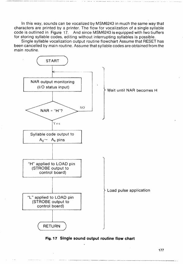
In this way, sounds can be vocalized by MSM6243 in much the same way that characters are printed by a printer. The flow for vocalization of a single syllable code is outlined in Figure 17. And since MSM6243 is equipped with two buffers for storing syllable codes, editing without interrupting syllables is possible.
Single syllable vocalization output routine flowchart Assume that RESET has been cancelled by main routine. Assume that syllable codes are obtained from the main routine.
( START)
~---------NAR output monitoring
(1/0 status input)
Syllable code output to
Ao~ As pins
"H" applied to LOAD pin (STROBE output to
control board)
1 "L" applied to LOAD pin
(STROBE output to control board)
NO
____ --oJ
~
Wait until NAR becomes H
Load pulse application
Fig. 17 Single sound output routine flow chart
177
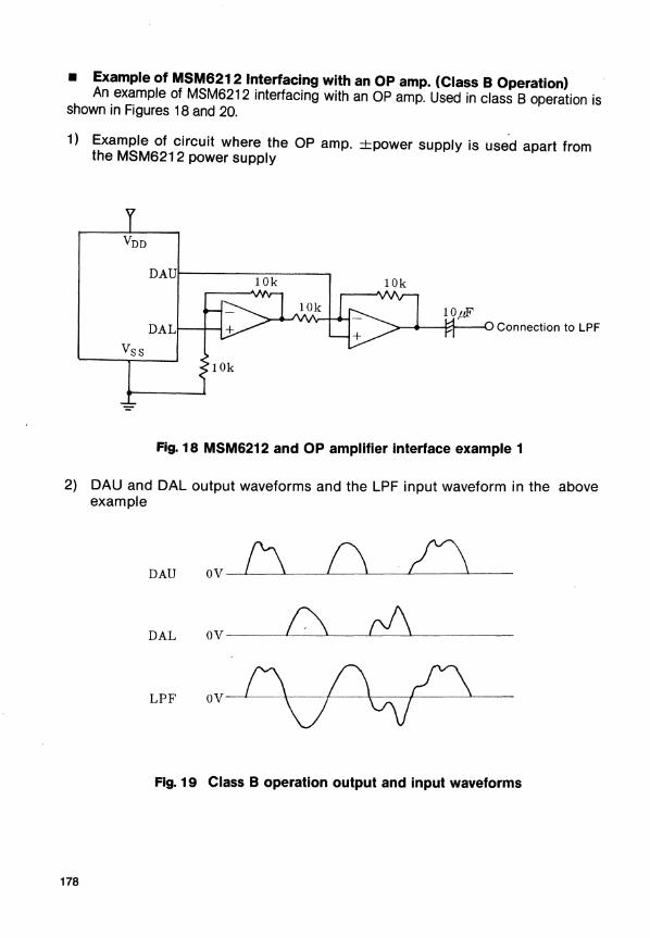
• Example of MSM6212 Interfacing with an OP amp. (Class B Operation) An example of MSM6212 interfacing with an OP amp. Used in class B operation is
shown in Figures 18 and 20.
1) Example of circuit where the OP amp. +power supply is used apart from the MSM6212 power supply
VDD
DAU~-------1-0-k----~ 10k
DAL·I---+--I '>--+--Y-I--.() Connection to LPF
Vss 10k
Fig. 18 MSM6212 and OP amplifier interface example 1
2) DAU and DAL output waveforms and the LPF input waveform in the above example
DAU OV t\ f\ n DAL OV C\ d\
LPF OV CVf\P Fig. 19 Class B operation output and input waveforms
178
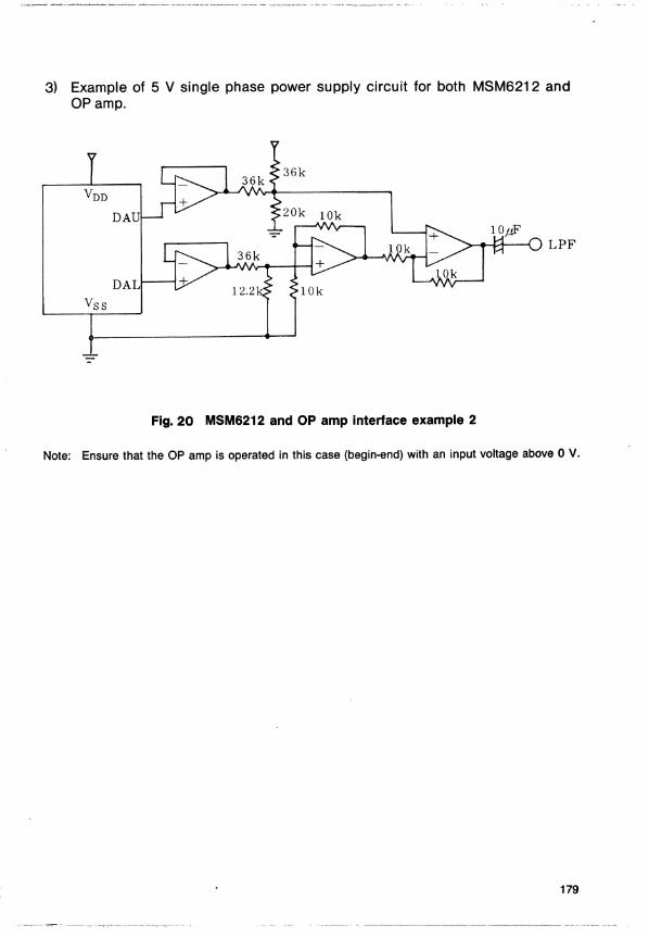
3) Example of 5 V single phase power supply circuit for both MSM6212 and OP amp.
LPF
Vss
Fig. 20 MSM6212 and OP amp interface example 2
Note: Ensure that the OP amp is operated in this case (begin-end) with an input voltage above 0 V.
179
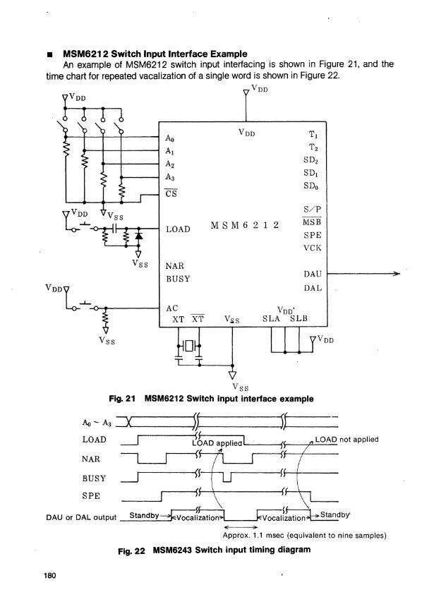
• MSM6212 Switch Input Interface Example An example of MSM6212 switch input interfacing is shown in Figure 21, and the
time chart for repeated vacalization of a single word is shown in Figure 22.
Vss
Ao Al A2 A3
cs
LOAD
NAR BUSY
VDD
VDD
MSM6212
Tl T2
SD2 SDl SDo
S/P MSB SPE VCK
V DDl....J---O--+-___ ---l AC
DAU I------~
DAL
VDD' SLA SLB XT XT Vss
Vss VDD
v ss Fig. 21 MSM6212 Switch input interface example
Ao - A3 .:=:x )f. ; )t
LOAD _I If LOAD applied l LOAD not applied
NAR ---, ~
BUSY ---.J ~f
SPE ~
DAU or DAL output StandbY~~~f!ationJ-:.StandbY' E ...
Approx. 1.1 msec (equivalent to nine samples)
Fig. 22 MSM6243 Switch input timing diagram
180
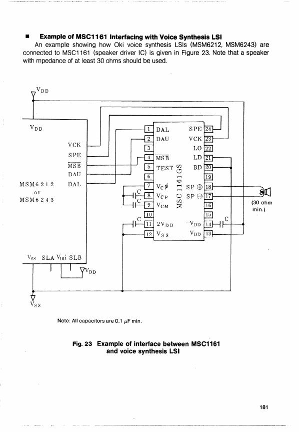
• Example of MSC1161 Interfacing with Voice Synthesis LSI An example showing how Oki voice synthesis LSls (MSM6212, MSM6243) are
connected to MSC1161 (speaker driver IC) is given in Figure 23. Note that a speaker with mpedance of at least 30 ohms should be used.
VDD SPE
VCK VCK LO SPE LD MSB 5 TEST rs BD DAD .....
MSM6212 DAL \0
vc1> ..... ..... or
VCP 0 MSM6243 Cf)
VCM ~
2VDD -VDD
Vss VDD
\'ss SLA VDD SLB
Vss
DD
Note: All capacitors are 0.1 JLF min.
Fig.23 Example of interface between MSC1161 and voice synthesis LSI
nJ (30 ohm min.)
181
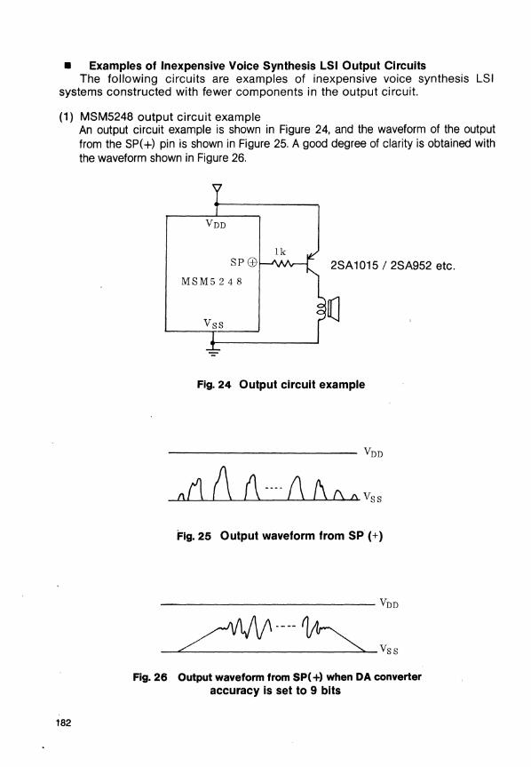
• Examples of Inexpensive Voice Synthesis LSI Output Circuits The following circuits are examples of inexpensive voice synthesis LSI
systems constructed with fewer components in the output circuit.
(1) MSM5248 output circuit example
182
An output circuit example is shown in Figure 24, and the waveform of the output from the SP(+) pin is shown in Figure 25. A good degree of clarity is obtained with the waveform shown in Figure 26.
lk S P (B "--""'''---'
MSM5248
Vss
2SA1015 / 2SA952 etc.
Fig. 24 Output circuit example
-------------------------- VDD
Fig.25 Output waveform from SP (+)
-----------------------------VDD
~~------~~vss Fig. 26 Output waveform from SP( +) when DA converter
accuracy is set to 9 bits
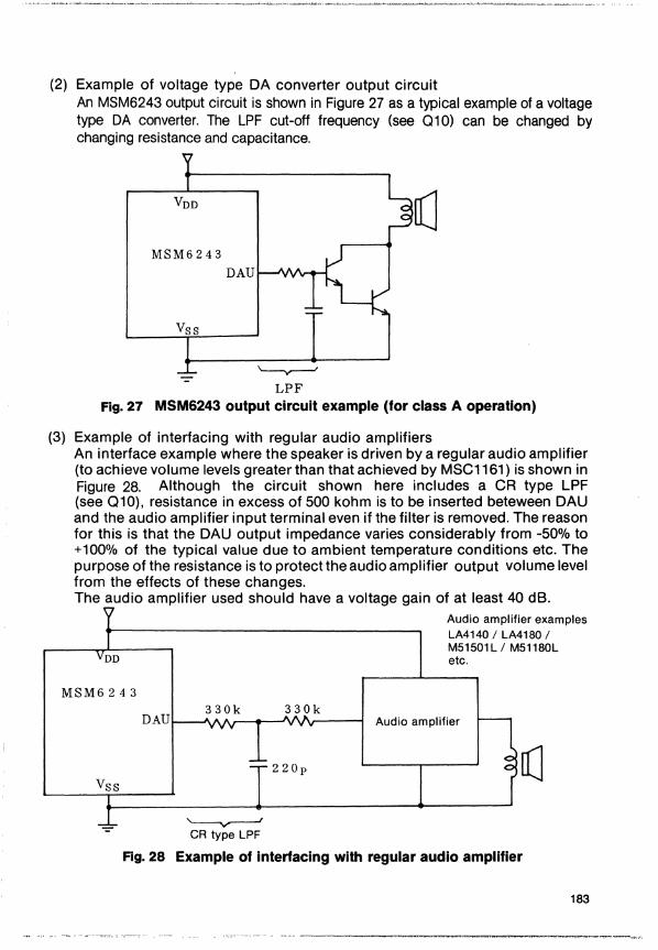
(2) Example of voltage type DA converter output circuit An MSM6243 output circuit is shown in Figure 27 as a typical example of a voltage type DA converter. The LPF cut-off frequency (see 010) can be changed by changing resistance and capacitance.
VDD
MSM6243 DAU I--J\I'o,~--'
Fig.27 MSM6243 output circuit example (for class A operation)
(3) Example of interfacing with regular audio amplifiers An interface example where the speaker is driven by a regular audio amplifier (to achieve volume levels greater than that achieved by MSC1161) is shown in Figure 28. Although the circuit shown here includes a CR type LPF (see 010), resistance in excess of 500 kohm is to be inserted beteween DAU and the audio amplifier input terminal even if the filter is removed. The reason for this is that the DAU output impedance varies considerably from -50% to +100% of the typical value due to ambient temperature conditions etc. The purpose of the resistance is to protect the audio amplifier output volume level from the effects of these changes. The audio amplifier used should have a voltage gain of at least 40 dB.
MSM6243
Vss
330k 330k DAU~-J\AJ\~-+--~~----~
'----y----J CR type LPF
Audio amplifier examples LA4140/ LA4180 / M51501L1 M51180L etc.
Audio amplifier
Fig. 28 Example of interfacing with regular audio amplifier
183
- ... -.---~--.---.~~--~-~.
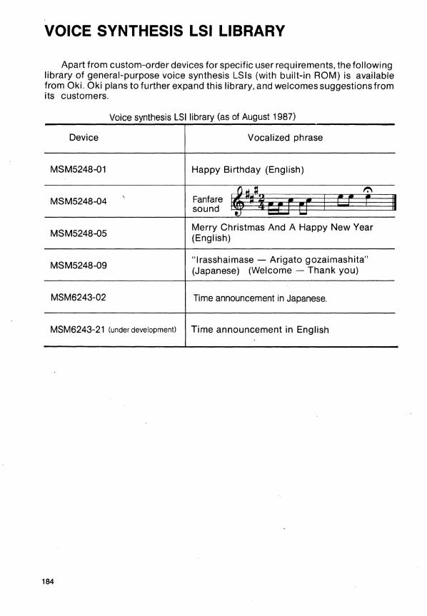
VOICE SYNTHESIS LSI LIBRARY
Apart from custom-order devices for specific user requi rements, the following library of general-purpose voice synthesis LSls (with built-in ROM) is available from Oki. Oki plans to further expand this library, and welcomes suggestions from its customers.
Voice synthesis LSI library (as of August 1987)
Device Vocalized phrase
MSM5248-01 Happy Birthday (English)
I~"a~ •• 1':'1
MSM5248-04 " Fanfare I ~ ~ II sound W=~
MSM5248-05 Merry Christmas And A Happy New Year (English)
MSM5248-09 "Irasshaimase - Arigato gozaimashita" (Japanese) (Welcome - Thank you)
MSM6243-02 Time announcement in Japanese.
MSM6243-21 (under development) Time announcement in English
184
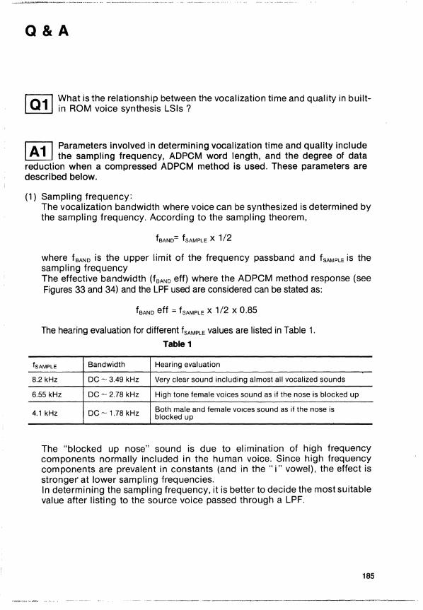
Q&A
I Q11 What is the relationship between the vocalization time and quality in builtin ROM voice synthesis LSls ?
I A1 I Parameters involved in determining vocalization time and quality include the sampling frequency, ADPCM word length, and the degree of data
reduction when a compressed ADPCM method is used. These parameters are described below.
(1) Sampling frequency: The vocalization bandwidth where voice can be synthesized is determined by the sampling frequency. According to the sampling theorem,
fBAND= fSAMPLE x 1/2
where f BAND is the upper limit of the frequency passband and fSAMPLE is the sampling frequency The effective bandwidth (fBAND eff) where the ADPCM method response (see Figures 33 and 34) and the LPF used are considered can be stated as:
f BAND eft = f SAMPLE X 112 x 0.85
The hearing evaluation for different fSAMPLE values are listed in Table 1.
Table 1
fSAMPLE Bandwidth Hearing evaluation
8.2 kHz DC - 3.49 kHz Very clear sound including almost all vocalized sounds
6.55 kHz DC - 2.78 kHz High tone female voices sound as if the nose is blocked up
4.1 kHz DC -1.78 kHz Both male and female vOices sound as if the nose is blocked up
The "blocked up nose" sound is due to elimination of high frequency components normally included in the human voice. Since high frequency components are prevalent in constants (and in the" i" vowel), the effect is stronger at lower sampling frequencies. In determining the sampling frequency, it is better to decide the most suitable value after listing to the source voice passed through a LPF.
185
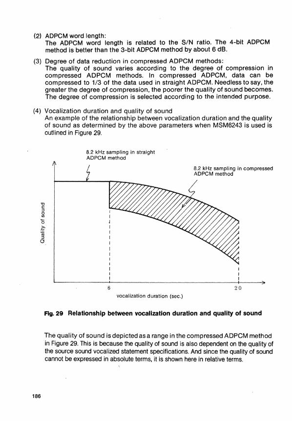
(2) ADPCM word length: The ADPCM word length is related to the SIN ratio. The 4-bit ADPCM method is beUer than the 3-bit ADPCM method by about 6 dB.
(3) Degree of data reduction in compressed ADPCM methods: The quality of sound varies according to the degree of compression in compressed ADPCM methods. In compressed ADPCM, data can be compressed to 1/3 of the data used in straight ADPCM. Needless to say, the greater the degree of compression, the poorer the quality of sound becomes. The degr.ee of compression is selected according to the intended purpose.
(4) Vocalization duration and quality of sound
"0 C
'" o (/)
An example of the relationship between vocalization duration and the quality of sound as determined by the above parameters when MSM6243 is used is outlined in Figure 29.
8.2 kHz sampling in straight ADPCM method
8.2 kHz sampling in compressed ADPCM method
'0 .£ m
'" a
186
20 vocalization duration (sec.)
Fig. 29 Relationship between vocalization duration and quality of sound
The quality of sound is depicted as a range in the compressed ADPCM method in Figure 29. This is because the quality of sound is also dependent on the quality of the source sound vocalized statement specifications. And since the quality of sound cannot be expressed in absolute terms, it is shown here in relative terms.
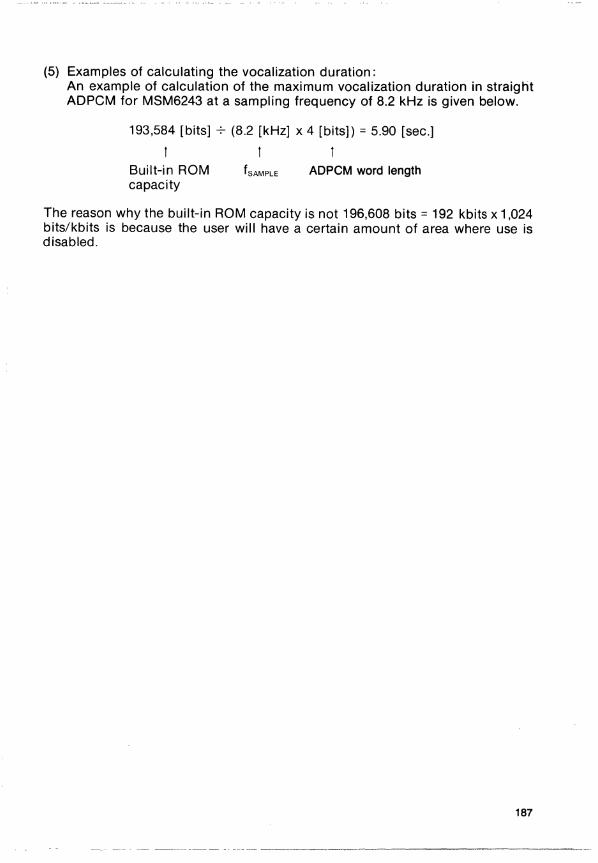
(5) Examples of calculating the vocalization duration: An example of calculation of the maximum vocalization duration in straight ADPCM for MSM6243 at a sampling frequency of 8.2 kHz is given below.
193,584 [bits] -7- (8.2 [kHz] x 4 [bits]) = 5.90 [sec.]
1 1 1 Built-in ROM capacity
fSAMPLE ADPCM word length
The reason why the built-in ROM capacity is not 196,608 bits = 192 kbits x 1,024 bits/kbits is because the user will have a certain amount of area where use is disabled.
187
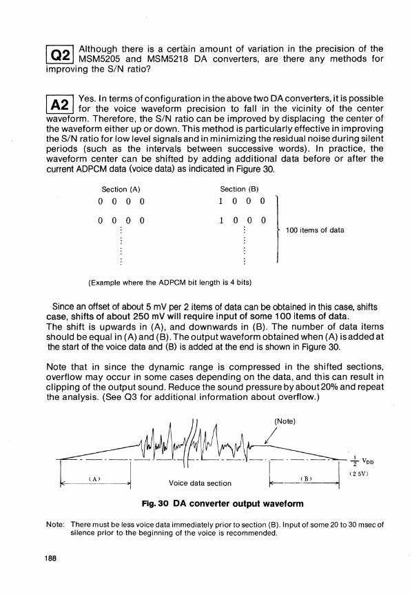
I Q21 Although there is a certain amount of variation in the precision of the MSM5205 and MSM5218 DA converters, are there any methods for
improving the SIN ratio?
I A21 Yes. In terms of configuration in the above two DA converters, it is possible for the voice waveform precision to fall in the vicinity of the center
waveform. Therefore, the SIN ratio can be improved by displacing the center of the waveform either up or down. This method is particularly effective in improving the SIN ratio for low level signals and in minimizing the residual noise during silent periods (such as the intervals between successive words). In practice, the waveform center can be shifted by adding additional data before or after the current ADPCM data (voice data) as indicated in Figure 30.
Section (A)
o 0 0 0
o 0 0 0
Section (8)
1 000
1 000
(Example where the ADPCM bit length is 4 bits)
100 items of data
Since an offset of about 5 mV per 2 items of data can be obtained in this case, shifts case, shifts of about 250 mV will require input of some 100 items of data. The shift is upwards in (A), and downwards in (8). The number of data items should be equal in (A) and (8). The output waveform obtained when (A) isadded at the start of the voice data and (8) is added at the end is shown in Figure 30.
Note that in since the dynamic range is compressed in the shifted sections, overflow may occur in some cases depending on the data, and this can result in clipping of the output sound. Reduce the sound pressure by about20% and repeat the analysis. (See 03 for additional information about overflow.)
Voice data section
Fig. 30 DA converter output waveform
I TVDD
(25V)
Note: There must be less voice data immediately prior to section (8). Input of some 20 to 30 msec of silence prior to the beginning of the voice is recommended.
188
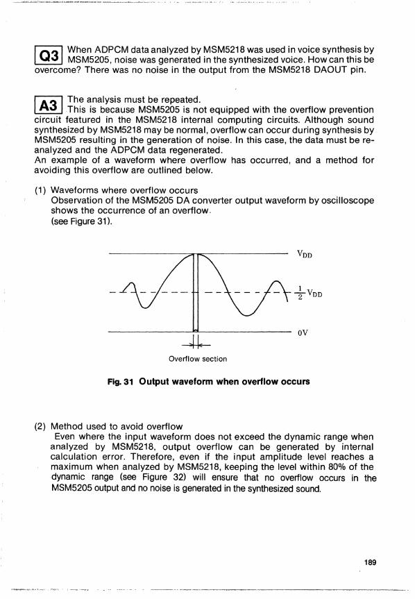
I Q31 When ADPCM data analyzed by MSM5218 was used invoice synthesis by MSM5205, noise was generated in the synthesized voice. How can this be
overcome? There was no noise in the output from the MSM5218 DAOUT pin.
I A31 The analysis must be repeated. This is because MSM5205 is not equipped with the overflow prevention
circuit featured in the MSM5218 internal computing circuits. Although sound synthesized by MSM5218 may be normal, overflow can occur during synthesis by MSM5205 resulting in the generation of noise. In this case, the data must be reanalyzed and the ADPCM data regenerated. An example of a waveform where overflow has occurred, and a method for avoiding this overflow are outlined below.
(1) Waveforms where overflow occurs Observation of the MSM5205 DA converter output waveform by oscilloscope shows the occurrence of an overflow. (see Figure 31).
Overflow section
Fig. 31 Output waveform when overflow occurs
(2) Method used to avoid overflow Even where the input waveform does not exceed the dynamic range when
analyzed by MSM5218, output overflow can be generated by internal calculation error. Therefore, even if the input amplitude level reaches a maximum when analyzed by MSM5218, keeping the level within 80% of the dynamic range (see Figure 32) will ensure that no overflow occurs in the MSM5205 output and no noise is generated in the synthesized sound.
189
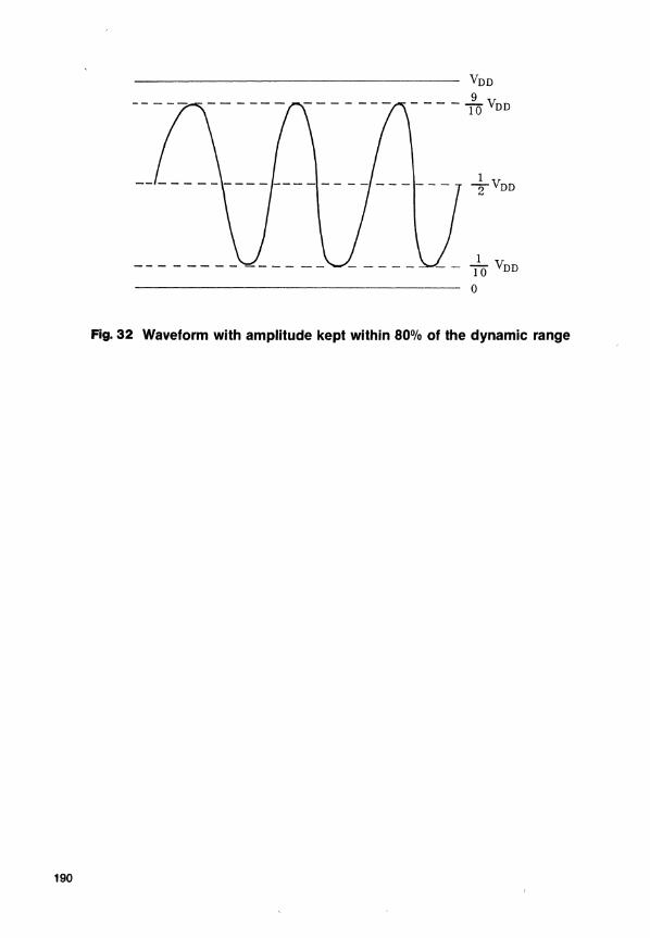
190
VDD
9 - - - - 10 VDD
1 Z-VDD
1 10 VDD
o
Fig. 32 Waveform with amplitude kept within 80% of the dynamic range
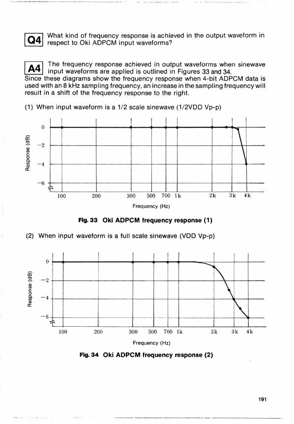
What kind of frequency response is achieved in the output waveform in respect to Oki ADPCM input waveforms?
I A41 The frequency response achieved in output waveforms when sinewave input waveforms are applied is outlined in Figures 33 and 34.
Since these diagrams show the frequency response when 4-bit ADPCM data is used with an 8 kHz sampling frequency, an increase in the sampling frequency will result in a shift of the frequency response to the right.
(1) When input waveform is a 1/2 scale sinewave (1/2VDD Vp-p)
0
iii' ~ -2 Q) en c: 0 a. " \ en -4 Q)
cc
-6 ...;
100 200 300 500 700 1k 2k 3k 4k
Frequency (Hz)
Fig.33 Oki ADPCM frequency response (1)
(2) When input waveform is a full scale sinewave (VDD Vp-p)
0
iii' ~ -2 Q) en c: 0 a. -4 en Q)
cc
-6
-.......,
1\ \
f--- ~ :::
100 200 300 500 700 lk 2k 3k 4k
Frequency (Hz)
Fig. 34 Oki ADPCM frequency response (2)
191
1 osl What does it mean to say that the DA converter output from MSM6243 etc is a "class A output" or "class B output"?
1 Asl MSM6243 and other devices are equipped with two DA converter output pins DAU and DAL. In class A output mode (the normal mode), the output
waveform only appears at the DAU pin with the VDD/2 potential at the amplitude center to obtain maximum amplitude for Vss thru VDD. Class B output mode is used in interfacing with MSC1161 (note). The upper half of the waveform above the class A output amplitude center appears at the DAU pin and the lower half of the waveform appears at the DAL pin with the main amplitude direction as the positive direction. The comparative waveforms are shown in Figure 35.
Where class B is multiplied by 1, the amplitude scale istwicethe class A level, and likewise class B multiplied by 2 and 4 result in class A multiplied by 4 and 8 respectively. In waveforms where the VDD level is exceeded, however, the output is clamped at Voo·
Note: The method described in MSM6212 Switch Input Interface Example at page 174.
192
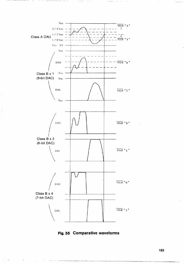
VUD
3/4 VUIJ -
1/2 Vou Class A DAU
1/4 VI)[)
MS H • 0 •
1
----j
_____ ~lSB·l·
v" OV -+--------+--
Class B x 1 v" (9-bit DAC) VIlIJ
\"':"
Class B x 2 (8-bit DAC)
\'"
Class B x 4 (7-bit DAC)
- - -- MSB '0'
Fig. 35 Comparative waveforms
193
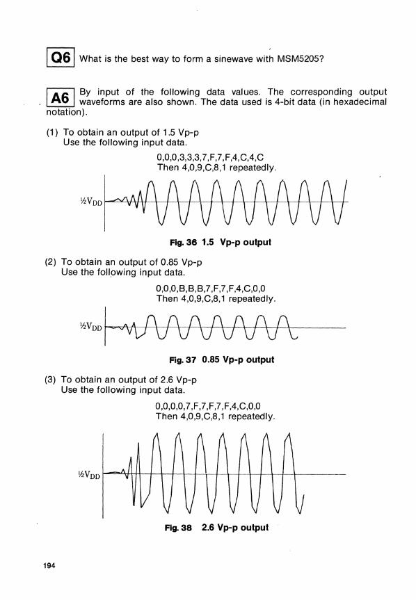
1 QSI What is the best way to form a sinewave wit~ MSM5205?
fA"I;ls By input of the following data values. The corresponding output . ~ waveforms are also shown. The data used is 4-bit data (in hexadecimal
notation).
(1) To obtain an output of 1.5 Vp-p Use the following input data.
0,0,0,3,3,3,7,F,7,F,4,C,4,C Then 4,0,9,C,8,1 repeatedly.
Fig. 36 1.5 Vp-p output
(2) To obtain an output of 0.85 Vp-p Use the foll,owing input data.
0,0,0,B,B,B,7,F,7,F,4,C,0,0 Then 4,0,9,C,8,1 repeatedly.
~VDDI-~t----Fig. 37 0.85 Vp-p output
(3) To obtain an output of 2.6 Vp-p
194
Use the following input data.
0,0,0,0,7,F,7,F,7,F,4,C,0,0 Then 4,0,9,C,8,1 repeatedly.
Fig. 38 2.6 Vp-p output
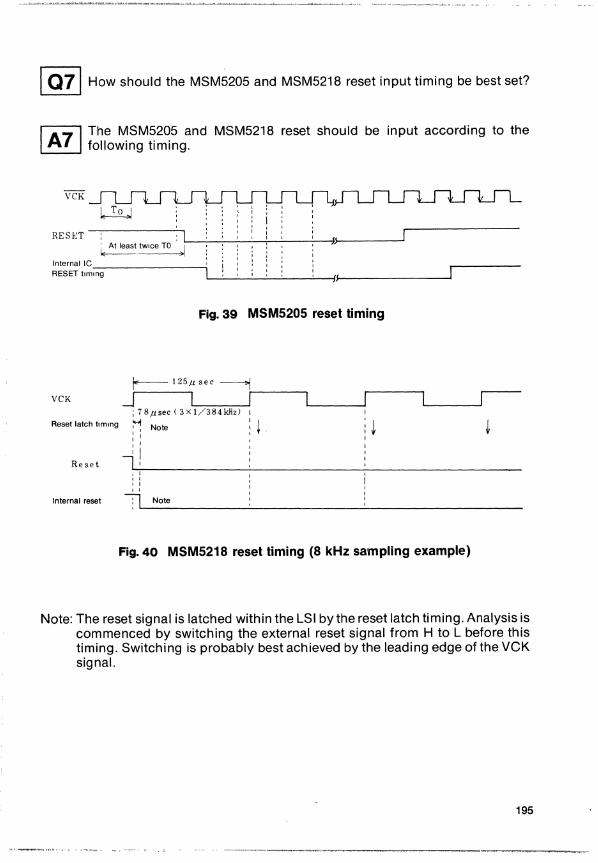
1 Q71 How should the MSM5205 and MSM5218 reset input timing be best set?
I A71 The MSM5205 and MSM5218 reset should be input according to the following timing.
InternaIIC _______ -i RESET timing L-'--'--'--'--'---'---jJJ~----------I
Fig. 39 MSM5205 reset timing
r----- 1 25/1 sec -----1 VCK J 1 ;""'1 ---, I
; 78,usec(3Xl/384kHz) I L--__ -l
Reset latch timing ~ Note ; ! ~ I I I I
! I Reset I~,I ______ ~ _______ ~ __________ _
! I ! I I I I I
Internal reset --n Note
Fig.40 MSM5218 reset timing (8 kHz sampling example)
Note: The reset signal is latched within the LSI by the reset latch timing. Analysis is commenced by switching the external reset signal from H to L before this timing. Switching is probably best achieved by the leading edge of the VCK signal.
195
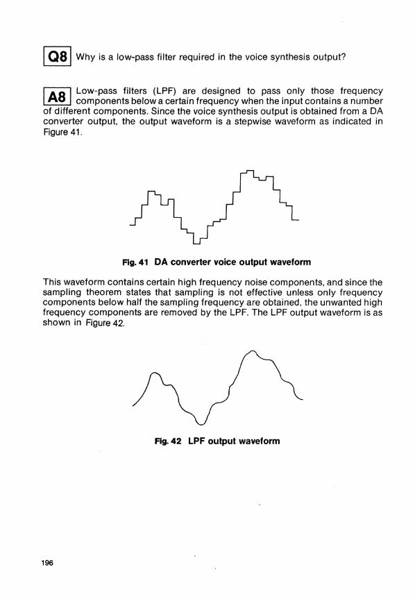
I QSI Why is a low-pass filter required in the voice synthesis output?
I Asl Low-pass filters (LPF) are designed to pass only those frequency components below a certain frequency when the input contains a number
of different components. Since the voice synthesis output is obtained from a DA converter output, the output waveform is a stepwise waveform as indicated in Figure 41.
Fig. 41 DA converter voice output waveform
This waveform contains certain high frequency noise components, and since the sampling theorem states that sampling is not effective unless only frequency components below half the sampling frequency are obtained, the unwanted high frequency components are removed by the LPF. The LPF output waveform is as shown in Figure 42.
Fig. 42 LPF output waveform
196
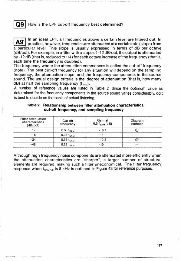
I osl How is the LPF cut-off frequency best determined?
fAft.ls' In an ideal LPF, all frequencies above a certain level are filtered out. In ~ practice, however, frequencies are attenuated at a certain rate (slope) from a particular level. This slope is usually expressed in terms of dB per octave (dB/oct). For example, in a filter with a slope of-12 dB/oct, the output is attenuated by -12 dB (that is, reduced to 1/4) for each octave increase of the frequency (that is, each time the frequency is doubled). The frequency where the attenuation commences is called the cut-off frequency (note). The best cut-off frequency for any situation will depend on the sampling frequency, the attenuation slope, and the frequency components in the source sound. The usual design criteria is the degree of attenuation (that is, how many dB) at half the sampling frequency (fSAM)' A number of reference values are listed in Table 2. Since the optimum value as determined for the frequency components in the source sound varies considerably, ddit is best to decide on the basis of actual listening.
Table 2 Relationship between filter attenuation characteristics, cut-off frequency, and sampling frequency
Filter attenuation Cut-off Gain at Diagram characteristics (dB/oct) frequency 0.5 fSAM (dB) number
-12 0.3 fSAM - 8.7 <D -18 0.33 fSAM -11 -
-24 0.35 fSAM -12.5 CD -48 0.38 fSAM -19 -
Although high frequency noise components are attenuated more efficiently when the attenuation characteristics are "sharper", a larger number of structural elements are required, making such a filter uneconomical. The filter frequency response when fSAMPLE is 8 kHz is outlined in Figure 43 for reference purposes.
197
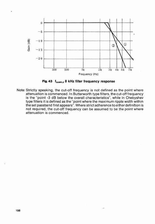
0
-5
iii' -10 2-.S a:! -15 (9
-20
~ ~ \ (2)' [\\ CD
\. --_ ..
\ \ I\.
\ ..
.300 500 lk 2k 3k 4k 5k 7k
Frequency (Hz)
Fig. 43 fSAMPLE 8 kHz filter frequency response
Note: Strictly speaking, the cut-off frequency is not defined as the point where attenuation is commenced. I n Butterworth type filters, the cut-off frequency is the "point -3 dB below the overall characteristics", while in Chebyshev type filters it is defined as the "point where the maximum ripple width within the set passband first appears". Where strict adherence to eitherdefinilion is not required, the cut-off frequency can be assumed to be the point where attenuation is commenced.
198
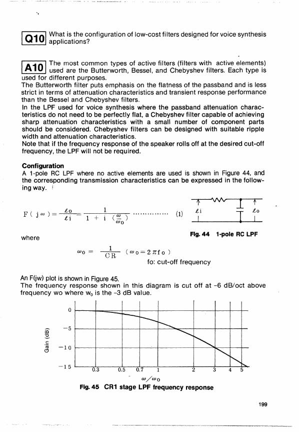
"
1 Q1 01 Wha~ is ~he configuration of low-cost filters designed for voice synthesis applications?
I A1 0 I The most common types of active filters (filters with active elements) used are the Butterworth, Bessel, and Chebyshev filters. Each type is
used for different purposes. The Butterworth filter puts emphasis on the flatness of the passband and is less strict in terms of attenuation characteristics and transient response performance than the Bessel and Chebyshev filters. In the LPF used for voice synthesis where the passband attenuation characteristics do not need to be perfectly flat, a Chebyshev filter capable of achieving sharp attenuation characteristics with a small number of component parts should be considered. Chebyshev filters can be designed with suitable ripple width and attenuation characteristics. Note that if the frequency response of the speaker rolls off at the desired cut-off frequency, the LPF will not be required.
Configuration A 1-pole RC LPF where no active elements are used is shown in Figure 44, and the corresponding transmission characteristics can be expressed in the following way. i
Lo Fejw)= Li
where
1 +
Wo =
1 e ~ ) ...............
Wo
1 OR e w 0 = 2 71:f 0 )
(1)
l' '\N'v 1 f Li
J Lo
I I
Fig. 44 1-pole RC LPF
fa: cut-off frequency
An Ffjw) plot is shown in Figure 45. The frequency response shown in this diagram is cut off at -6 dB/oct above frequency wo where Wo is the -3 dB value.
0
iD -5
~ c: 'iii -10 C)
-15
r-------I'--.... -......... ~
"-... "'-r-..
0.3 0.5 0.7 1 2 3 4 5
w/wo Flg.45 CR1 stage LPF frequency response
199
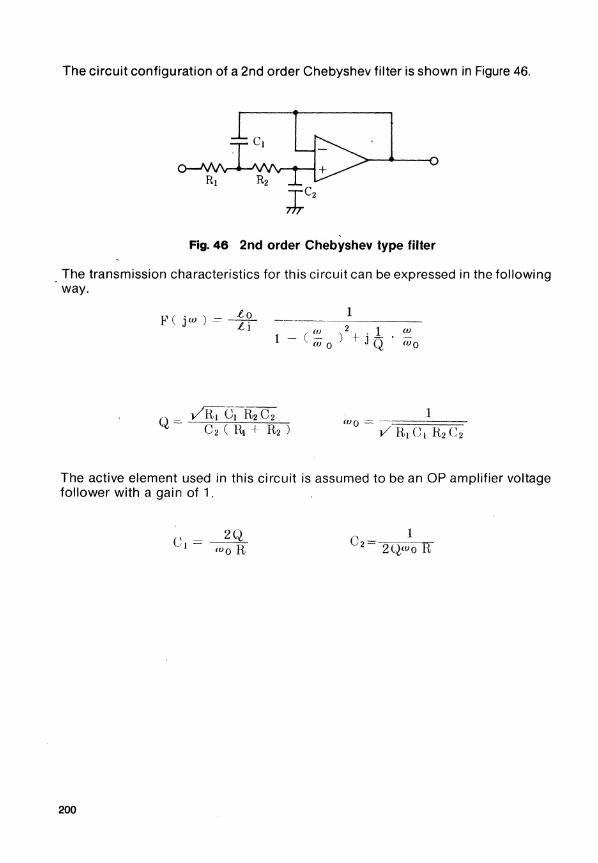
The circuit configuration of a 2nd order Chebyshev filter is shown in Figure 46.
,
Fig. 46 2nd order Chebyshev type filter
_ The transmission characteristics for this circuit can be expressed in the following way.
l~ (. ) _ -to r " J IV '----z-r- 1
IV 2 1 1-(- )+j-
IVo Q IV
IVo
The active element used in this circuit is assumed to be an OP amplifier voltage follower with a gain of 1.
u - 2(~ J - IVo R
200
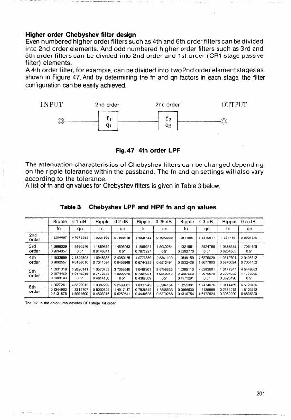
Higher order Chebyshev filter design Even numbered higher order filters such as 4th and 6th order filters can be divided into 2nd order elements. And odd numbered higher order filters such as 3rd and 5th order filters can be divided into 2nd order and 1 st order (CR1 stage passive filter) elements. A 4th order filter, for example, can be divided into two 2nd order element stages as shown in Figure 47. And by determining the fn and qn factors in each stage, the filter configuration can be easily achieved.
INPUT 2nd order 2nd order OUTPUT
©----!
Fig.47 4th order LPF
The attenuation characteristics of Chebyshev filters can be changed depending on the ripple tolerance within the passband. The fn and qn settings will also vary according to the tolerance. A list of fn and qn values for Chebyshev filters is given in Table 3 below.
Table 3 Chebyshev LPF and HPF tn and qn values
Ripple = 0 1 dB Ripple = 0 2 dB Ripple = 0.25 dB Ripple = 03 dB Ripple = 0 5 dB
In qn In qn In qn In qn In qn
2nd 1 8204497 07673593 15351966 07966418 1 4539722 08092536 1 3911667 08210811 1231418 08637210 order
3rd 12999029 13490276 11889612 1 4595033 11569921 15080264 11321861 1 5524768 10868535 1 7061895 order 09694057 05" 08146341 05" 07672227 05" 07292773 05" 06254565 05"
4th 11532699 21829303 10948338 24350125 10779389 25361100 10648159 26279020 10312704 29405542 order 07892557 06188010 07011094 06458968 06744223 06572494 06532428 08677803 05970024 07051102
5th 10931318 32820141 1 0570753 37068586 10466301 38756825 10385110 40283601 10177347 45449633
order 07974460 09145215 07472558 10009079 07324054 1 0359319 07207553 1 0678979 06904832 1 1778056 05389143 05" 04614106 05" 04369509 05" 04171291 05" 03623196 05"
6th 1 0627261 46329012 10382299 52689021 10311242 55204164 1 0255981 57474076 10114459 65128456
order 08344903 13315707 08030621 1 4917187 07938542 1 5556533 07866830 1 6135959 07681212 18103772 05131875 05994600 04603216 06259511 04440628 06370268 04310754 06472924 03962290 06836390
The 0 5* In the qn column denotes CR1 stage 1st order
201
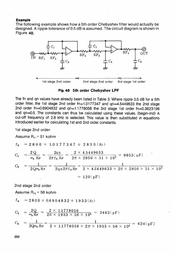
Example The following example shows how a 5th order Chebyshev filter would actually be designed. A ripple tolerance of 0.5 dB is assumed. The circuit diagram is shown in Figure 48.
1 st stage 2nd order 2nd stage 2nd order 3rd stage 1 st order
Fig. 48 5th order Chebyshev LPF
The fn and qn values have already been listed in Table 3. Where ripple 0.5 dB for a 5th order filter, the 1 st stage 2nd order fn=1.0177347 and qn=4.5449633 the 2nd stage 2nd order fn=0.6904832 and qn=1.1778056 the 3rd stage 1 st order fn=0.3623196 and qn=0.5. The constants can thus be calculated using these values. (begin-ind) A cut-off frequency of 2.8 kHz is selected. This value is then substituted in equations introduced earlier for calculating 1 st and 2nd order constants.
1 st stage 2nd order
Assume RF1 = 51 kohm
f 0 = 2 8 0 0 x 1.0 1 7 7 3 4 7 ::;:: 2 8 5 0 C Hz )
2Q 2qn 2 x 4.5449633 0 1 =--
CUo RF 2/Tfo RF 2/T x 2850 x 51 x 103
1 1 O2 2QcuoRF 2qn2/TfoRF 2 x 4.5449633 X
2nd stage 2nd order
Assume RF2 = 56 kohm
120CpF)
f 0 = 2800 x 0.6904832 ::;:: 1 933 (Hz)
= 9953(pF)
1 2/T x 2850 x
= ~ = 2 x 1.1778056 CUoRF 2/TX1933X56xI03
3463CpF)
51 X 103
__ ~1~= __________________ ~IL-__________ _ 2Qwo RF 2 x 1.1 7 7 8 0 5 6 x 2 /T X 1 933 x 5 6 x 1 03
624CpF)
202
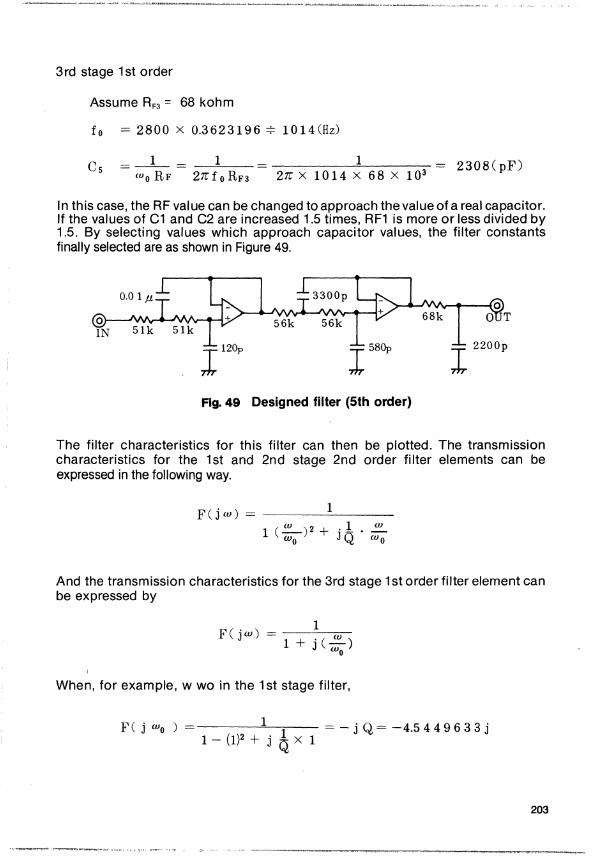
3rd stage 1 st order
Assume RF3 = 68 kohm
fo = 2800 x 0.3623196,* 1014CHz)
27r x 1014 ; 68 x 103 = 2308(pF)
In this case, the RF value can be changed to approach the value of a real capacitor. If the values of C1 and C2 are increased 1.5 times, RF1 is more or less divided by 1.5. By selecting values which approach capacitor values, the filter constants finally selected are as shown in Figure 49.
r 580p r 2200p
Fig. 49 Designed filter (5th order)
The filter characteristics for this filter can then be plotted. The transmission characteristics for the 1 st and 2nd stage 2nd order filter elements can be expressed in the following way.
F (j w) = ____ 1 ___ _ w 1 w 1 (_)2 + J' - • -Wo Q Wo
And the transmission characteristics for the 3rd stage 1 st order filter element can be expressed by
FCjW)-I+·C.!:.!....) J Wo
1
When, for example, w wo in the 1st stage filter,
F ( j Wo ) = 1 = - j Q = - 4.5 4 4 9 6 3 3 j 1 - (1)2 + j ~ x 1
203
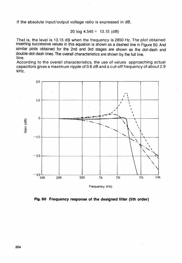
If the absolute input/output voltage ratio is expressed in dB,
20 log 4.545 = 13.15 (dB)
That is, the level is 13.15 dB when the frequency is 2850 Hz. The plot obtained inserting successive values in this equation is shown as a dashed line in Figure 50. And similar plots obtained for the 2nd and 3rd stages are shown as the dot-dash and double-dot-dash lines. The overall characteristics are shown by the full line. line. According to the overall characteristics, the use of values approaching actual capacitors gives a maximum ripple of 0.6 dB and a cut-off frequency of about 2.9 kHz.
iiJ :s. c: 'iii (!l
204
20
10
0
-10
-20
-30 100 200
, \
I \ \
/ \ / \
",' \ ". \
....-.,J'.--...:. .. :-~"':"-"'"
Do. \ ·_-t ~\ \
.......... \ ...........
"'. \
r \
500 lk 2k
Frequency (Hz)
I I
, \
, . ~ ,
t-.. , . "', \~
". , \
\
5k 10k
Fig. 50 Frequency response of the designed filter (5th order)
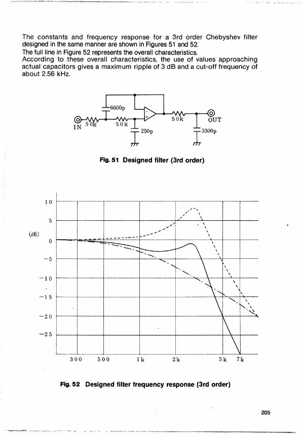
The constants and frequency response for a 3rd order Chebyshev filter designed in the same manner are shown in Figures 51 and 52. The full line in Figure 52 represents the overall characteristics. According to these overall characteristics, the use of values approaching actual capacitors gives a maximum ripple of 3 dB and a cut-off frequency of about 2.56 kHz.
r3300P
Fig. 51 Designed filter (3rd order)
10
I , .. '" -, , \
/ \
5 .- \
.- .- \
(dB) 0
-5
-10
-15
-20
, , \
--' \ - - - ------- ---\ . . . --:-::::::- U
\
t:-, \ -" \
......... \
...... , ..... \ \
1'. \
\
" \
r---
"~, ,
\
,
\1 " , , \
) i'.~
-25 1\ \
300 500 1k 2k 5k 7k
Fig. 52 Designed filter frequency response (3rd order)
205
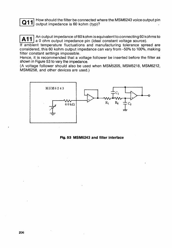
I Q111 How should the filterbe connected where the MSM6243 voice output pin output impedance is 60 kohm (typ)? •
I A111 An output impedance of60 kohm iseql,Jivalenttoconnecting60 kohms to a 0 ohm output impedance pin (ideal constant voltage source).
If ambient temperature fluctuations and manufacturing tolerance spread are considered, this 60 kohm output impedance can vary from -50% to 100%, making filter constant settings impossible. Hence, it is recommended that a voltage follower be inserted before the filter as shown in Figure 53 to vary the impedance. (A voltage follower should also be used when MSM5205, MSM5218, MSM6212, MSM6258, and other devices are used.)
MSM6243
Fig.53 MSM6243 and filter interface
206
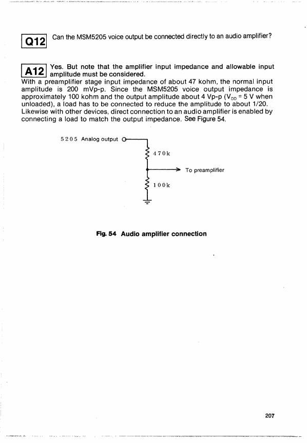
1 Q121 Can the MSM5205 voice output be connected directly to an audio amplifier?
I A121 Yes. But note that the amplifier input impedance and allowable input amplitude must be considered.
With a preamplifier stage input impedance of about 47 kohm, the normal input amplitude is 200 mVp-p. Since the MSM5205 voice output impedance is approximately 100 kohm and the output amplitude about 4 Vp-p (VDD = 5 V when unloaded), a load has to be connected to reduce the amplitude to about 1/20. Likewise with other devices, direct connection to an audio amplifier is enabled by connecting a load to match the output impedance. See Figure 54.
52 0 5 Analog output 0-----,
470k
To preamplifier
lOOk
Fig. 54 Audio amplifier connection
207

Note : Product data and specification information herein are subject to change without advance notice for the sake of technical improvements in performance and reliability since OKI is permanently endeavoring to supply the best products possible. The manufacturer does not assume responsibi lity for customer product designs and for the fitness to any particular application, nor for patent rights or other rights of third parties and infringements thereof resulting from the use of his products. This publication does not commit immediate availability of the product(s) described by it. If in doubt, please contact your nearest OKI representative . The information furnished by OKI is believed to be accurate and reliable. However, no responsibil ity is assumed for inaccuracies that may not have been detected prior to printing, and for those wh ich occur beyond our control . This issue substitutes and supersedes all publications previously supplied by OKI for the captioned product(s). This document may not, in whole or part, be copied, photocopied , reproduced , translated , or converted to any machine readable form, without prior written consent from OK!. r- ..
Oki Semiconductor 785 North Mary Avenue, Sunnyvale, CA 94086-2909
Tel : (408) 720-1900 Fax: (408) 720 -1918
FOR FURTHER INFORMATION PLEASE CONTACT :
OKI
Pr inted in USA