NSF US-EU Workshop on 2D Layered Materials and...
53
1 NSF US-EU Workshop on 2D Layered Materials and Devices April 22-24, 2015, Arlington, VA, USA Workshop Final Report Submitted to the NSF by: Anupama Kaul, University of Texas, El Paso, TX, U.S.A. James Hwang, Lehigh University, PA, U.S.A. http://engineering.utep.edu/useu2dworkshop/ Disclaimer: The views expressed are those of the authors and do not necessarily reflect the views of the National Science Foundation
Transcript of NSF US-EU Workshop on 2D Layered Materials and...

1
NSF US-EU Workshop on
2D Layered Materials and Devices
April 22-24, 2015, Arlington, VA, USA
Workshop Final Report Submitted to the NSF by:
Anupama Kaul, University of Texas, El Paso, TX, U.S.A. James Hwang, Lehigh University, PA, U.S.A.
http://engineering.utep.edu/useu2dworkshop/
Disclaimer: The views expressed are those of the authors and do not necessarily reflect the views of the
National Science Foundation

2
NSF US EU Workshop on 2D Layered Materials and Devices
Sponsorship: NSF, UTEP, AFRL, and STARnet
Workshop Organizing Committee and Break-out leaders
Organizing Committee
US Workshop Chair and Co-chair
EU Workshop Chair and Co-chairs
US Workshop Chair: Professor Anupama B. Kaul
[email protected] Associate Dean for Research and Innovation AT&T Distinguished Professor MME & ECE (joint) The University of Texas at El Paso, El Paso, TX, USA
US Workshop Co-chair: Professor James Hwang
[email protected] Director of Compound Semiconductor Laboratory Department of Electrical and Computer Engineering Lehigh University, Bethlehem, PA, USA
EU Workshop Chair: Professor Jari Kinaret
[email protected] Director of Graphene Flagship Department of Applied Physics Chalmers University of Technology, Gothenburg, Sweden, EU

3
Steering Committee
Program Manager
EU Workshop Co-chair: Professor Vladimir Falko
[email protected] Distinguished Professor Department of Physics- Lancaster University, England, United Kingdom, EU
EU Workshop Co-chair: Professor Andras Kis
[email protected] Director for Laboratory of Nanoscale Electronics and Structures, EPFL, Switzerland, EU
Dr. Wide Hogenhout
[email protected] European Commission Directorate-General for Communications Networks, Content and Technology; Directorate C 'Excellence in Science' - Unit 'Flagships'; Office BU33 6/53 B-1049 Belgium, EU
Dr. Dimitris Pavlidis
[email protected] Program Director, Engineering Directorate National Science Foundation, Arlington, VA, USA
Dr. Sandra Aguirre-Covarrubias
[email protected] Assistant Director for Research, College of Engineering The University of Texas at El Paso, El Paso, TX, USA

4
Break-out Leaders
Material Properties and Devices
Theory, Modeling and Simulation
Synthesis and Scalability
http://engineering.utep.edu/useu2dworkshop/
Professor Vivek Shenoy
US Break-out Chair
[email protected] MSE, BE, MEAM School of Engineering and Applied Science, University of Pennsylvania, Philadelphia, PA, USA
Professor Guido Burkard
EU Break-out Chair
Guido.Burkard@uni-
konstanz.de
Department of Physics
University of Konstanz,
Germany, EU
Professor Evan Reed
Scribe
[email protected] Assistant Professor Department of Materials Science and Engineering, Stanford University, Stanford, CA, USA
Professor Manish Chhowalla
US Break-out Chair
[email protected] Materials Science & Engineering, Rutgers, The State University of New Jersey, New Brunswick, NJ, USA
Professor Juerg Osterwalder
EU Break-out Chair
[email protected] Physics Institute University of Zurich Zurich, Switzerland , EU
Professor Mauricio Terrones
Scribe
[email protected] Physics, Chemistry and Materials Science and Engineering; Eberly College of Science; The Pennsylvania State University, State College, PA, USA
Professor Andras Kis
EU Break-out Chair
[email protected] Director for Laboratory of Nanoscale Electronics and Structures EPFL, Switzerland, EU
Professor Huili (Grace) Xing
US Break-out Chair
[email protected] Richard Lunquist Sesquicentennial Professor School of ECE & MSE, Cornell University, Ithaca, NY, USA
Professor Chun Ning (Jeanie) Lau
Scribe
Department of Physics
University of California, Riverside,
Riverside, CA, USA

5
1.0 Preface The ability to isolate or grow two-dimensional (2D) materials has been a source of scientific fascination ever since it was shown to be possible. This started with graphene, followed by various other 2D materials, and then by the ability to build custom-made structures (hetero-structures) by stacking combinations of 2D materials on top of each other and constructing libraries of crystals to provide specific electrical, thermal, physical or mechanical properties and functionalities. Today it is a field that spreads out from fundamental science to final products such as tennis rackets.
Research funders on both sides of the Atlantic have taken up the challenge of exploring the technological opportunities this has generated. Research linked to 2D materials has been taken up by various American research agencies, in particular linked to the US Department of Defence and the US Department of Energy, and on the European side by the European Research Council. In October 2013 the European Commission launched the Graphene FET Flagship, bringing together many European researchers around this topic, and in September 2013 the National Science Foundation (NSF) launched the Two-dimensional Atomic-layer Research and Engineering (2DARE) program.
The “US - EU Workshop on 2D Layered Materials and Devices”, held in Arlington, was set up to develop a shared understanding of research challenges in the area of layered 2D materials and explore opportunities for cross-Atlantic collaboration. It involved research communities from both sides, and resulted in a dynamic and open debate with a particular focus on three topics:
Materials Properties and Devices
Theory, Modelling and Simulation
Synthesis and Scalability
International collaboration in these areas can make a crucial contribution by bringing together complementary competencies, exchanging experience and injecting new ideas into research teams on both sides. This report contains many of the scientific insights into these questions that were put forward.
It has also given rise to a discussion about bilateral actions for mobility funding, enabling researchers from both sides of the Atlantic to work with a research team on the other side for some time. This is a first step towards jointly addressing some of the key issues that have been identified, such as the importance of interdisciplinary research leading to deeper interactions between different parts of the research community (e.g., material growers and device researchers), the role of technology-driven roadmaps, and cross-Atlantic exchange of information (e.g., information about material properties).

6
The next workshop has been planned for September 2016 in Europe, which will aim at further advancing our understanding of common research challenges in the field and further the discussion on the joint planning of research activities.
The workshop participants would like to acknowledge the assistance provided by Dr. Dimitris Pavlidis, NSF Program Director, and Dr. Wide Hogenhout, Programme Officer at the European Commission.

7
Table of Contents
Section Page No.
Cover Page and Organizing Committee…………………………………………………. 1
1.0 Preface……………………………………………………….……………………………………….. 5
2.0 Overview……………..………………………………………………………..……………………… 8 3.0 Agenda and List of Topics
3.1 Workshop Agenda……………………………………………………….………………… 13 3.2 List of Topics ….…………………………………………………………………..………… 18 3.3 List of Participants …………………..……….………………………………….………. 19 3.4 Picture Gallery……………………………………………………………………….……… 22
4.0 Technical Highlights & Break-out Summaries………………………………………. 23
4.1 Materials Properties and Devices………………………………………..……….. 25 4.1.1 Technical Highlights……………………………….……..………..….. 25 4.1.2 Report for Break-out Topic 1…….………..…………………..….. 32
4.2 Theory and Modeling ……………………………………………………………….…. 35 4.2.1 Technical Highlights….……………………………….…..……...…… 35 4.2.2 Report for Break-out Topic 2..………..………….……………….. 36
4.3 Synthesis and Scalability.…………………………………………………………….… 40 4.3.1 Technical Highlights….………………….……….………………….... 40 4.3.2 Report for Break-out Topic 3…….………..…………………..….. 42
5.0 Summary and Recommendations…………………………..……………………......... 43
References………………………………………………………………………………………….…. 48

8
2.0 Overview The idea of a joint United States (US) European Union (EU) Workshop on Two-dimensional (2D) Layered Materials and Devices was borne out of informal discussions held by researchers and administrators from the US and the EU at the Graphene Conference in Toulouse, France in May 2014. This 3-day workshop was particularly timely in bringing together a growing community of leading scientists from Europe and the US who are embarked on important fundamental research on 2D layered materials including graphene, and for addressing important challenges for this interdisciplinary field that lie ahead. Amongst the research challenges in the field of 2D layered materials are: a) devising techniques that can enable the scalable synthesis of these materials, b) controlling layer number and exploring growth on multiple substrates, c) understanding doping mechanisms and optimizing contacts for device research, d) utilizing interface-induced novel effects in planar and vertical heterostructures, e) developing predictive modeling and simulation techniques, and f) devising in situ and ex situ characterization techniques to measure material properties. The objective of this workshop was to provide an open technical forum that brings together leading researchers from the US and Europe to discuss cutting-edge research in the areas (a) – (f) outlined above.
Graphene, the thinnest material physically in existence, has a layered 2D atomic structure and has shown exceptional electronic, thermal, mechanical and optical properties.1,2 Exfoliated and vapor grown graphene, as well as a variety of other morphologies such as nanoribbons, have provided fascinating insights into how this material can be modified and fabricated into novel devices for applications such as transistors,3,4,5 circuits,6,7,8 interconnects,9,10 sensors,11 memory and spintronic devices,12,13,14 flexible electronics,15,16 ,17 and photonic devices and solar cells.18,19,20,21 The impressive body of work on graphene -- yielding more than 5,000 publications on average annually over the last decade -- has opened the opportunity to explore other 2D layered materials based on non-carbon compositions.22,23,24,25 For example, 2D hexagonal boron nitride (h-BN), transition metal di-chalcogenides (TMDCs), tertiary compounds of carbo-nitrides, and complex oxides such as clays and zeolites can be exfoliated and isolated as stable, single atomic layers.26,27,28
Given the wide range of compositions of 2D layered materials beyond graphene,29,30,31 they offer a rich spectrum of properties. One such property is the presence of an inherent and appreciable band gap. This inherent band gap, unlike graphene, coupled with the potential for atomically-smooth, pristine interfaces free of dangling bonds, can offer a unique platform for advancing research in nanoelectronics for example, to enable low-power and low-loss devices.32,33 Quantum-mechanical effects in these materials are equally intriguing, where 2D layered materials such as MoS2, WS2, WSe2, MoSe2 and MoTe2, undergo an indirect-to-direct band gap transition in going from the bulk to monolayers.34,35,36 Correlated behavior including superconductivity and charge density waves are also manifested at low temperatures in some 2D layered materials, such as NbSe2, TaS2 and Cu-intercalated TiSe2. The influence of mechanical strain on modulating the band gap of some 2D layered semiconducting materials is also a unique attribute of these systems, opening-up prospects for innovative opto-mechanical sensing devices, as another example.37,38,39,40

9
This field is currently experiencing intense activity in areas of material structure-property correlations, manufacturable synthesis and nanofabrication, device integration and device characterization studies; at the same time, modeling and simulation are also proving invaluable for predicting materials properties and new device functionalities. It is therefore extremely timely to have such a workshop focusing on capturing recent advances in 2D layered materials research that have the potential to impact fundamental science and discovery, as well as pushing new technological avenues for exploration in the future. At the core of this workshop was the opportunity to bring together leading experts in this area of research from the US and EU, where activity is being propelled by research investments made by both continents to support research in this area. Besides leveraging the expertise of researchers from these two geographical regions, the workshop also brought together experts with diverse technical backgrounds ranging from the basic sciences (e.g. physics, chemistry, computational sciences) as well as the engineering disciplines (materials, electrical, chemical and mechanical engineering), to promote discussions across disciplinary boundaries.
The venue for this workshop was the Holiday Inn in Arlington, Virginia, USA, and about 111 participants from academia, government laboratories, industry, and federal funding agencies convened as invited speakers, panelists, or guests. Figure 1 provides a mapping of the participant distribution at the workshop, in terms of (a) geography, and (b) sector. The workshop would not have been possible without the support from the National Science Foundation (NSF), specifically Dr. Dimitris Pavlidis from the Engineering Directorate, and the European Commission, specifically Dr. Wide Hogenhout, who both served as members of the Steering Committee, and helped guide the organization of this workshop. While this workshop provided a forum for researchers from the US and EU to share their work and engage in discussions, it should be noted that significant investments in 2D layered materials research have also taken place in Asia, as indicated in the summary of the major world-wide initiatives and centers in this area of research outlined in Figure 2.
US Participants EU Participants
Figure 1. (a) Geographical distribution of participants at the workshop from the US and Europe. (b) Breakdown of participants at workshop from the various sectors: academia, federal agencies, government labs and industry.
62%12%
19%
7%
Workshop Participants
Academia Government Lab
Federal Agency Industry
(a) (b)

10
The US Workshop Chair for this event was Prof. Anupama Kaul from the University of Texas, El Paso (UTEP). Prof. James Hwang, from Lehigh University, served as the US Workshop Co-chair. In their prior roles while on rotation serving in the federal government, specifically the NSF and the Air Force Office of Scientific Research (AFOSR), Prof. Anupama Kaul and Prof. James Hwang were instrumental in the creation of the NSF’s Emerging Frontiers in Research and Innovation (EFRI) 2-Dimensional Atomic-layer Research and Engineering (2-DARE) initiative, and the AFOSR, Basic Research Initiative (BRI) on 2D Materials and Devices Beyond Graphene, respectively. The NSF EFRI 2-DARE program solicited proposals in 2013 and 2014, and Prof. Dimitris Pavlidis has coordinated and is currently overseeing this initiative, while on assignment to the NSF from Boston University. The 2-DARE EFRI program has invested in areas that will play a major role in future generations of nanoelectronics, optoelectronics, as well as mechanical and bio-engineering. The 2014 2-DARE EFRI call also promoted device applications such as high-frequency components for signal treatment and generation, as well as power, highlighting the technological benefits from the proposed materials. Fundamental material properties, growth considerations, as well as device concepts, thermal management and related effects, have been some of the key areas of the proposed research activities and awards. These are expected to serve as an enabling platform for new device functionality and improved performance when compared to current technologies. The combined funding commitment of the EFRI 2-DARE and BRI programs exceeds more than $50 Million over a period of time extending from 2014 to 2019. NSF has also been supporting the 2-Dimensional atomic-layer materials and device technology research by a multi-million dollar investment through many other programs.
Meanwhile, the Graphene Flagship Project in Europe has 142 partners in 23 countries and is targeted at the level of $1 Billion Euros over the course of ten years; it also showcases a large industrial contingent. The Graphene Flagship is managed by Chalmers University of Technology, in Gothenburg, Sweden. Prof. Jari Kinaret from the Applied Physics Department at Chalmers University is the appointed Director of this EU Flagship, and he served as the EU Workshop Chair to lead activities of European researchers participating in this joint workshop. Prof. Vladimir Falko from Lancaster University, who leads the Flagship Work Package focused on the development of new 2D materials, and Prof. Andras Kis from the Ecole Polytechnique Federale de Lausanne (EPFL), both acted as a Co-chairs from the EU to help coordinate the participation of EU researchers at this workshop. Prior to the workshop, the organizing committee held several
Figure 2. World-wide initiatives and centers on 2D layered materials research.
World-wide Initiatives & Centers on 2D Layered Materials
Europe: Graphene Flagship Mission ($1Billion Euros/10 yrs); Manchester Graphene Center, etc.
USA: ARO / ARL – MURI on Beyond Graphene; NSF EFRI 2-DARE, AFOSR BRI Program; NIST Materials Initiative; SRC/NRI STARnet program; ONR / NRL – Initiative on Graphene and Beyond; ARO MURI on 2D Organic Materials; AFOSR – MURI on 2D for Flexible Electronics, etc.
Asia: Graphene Research Center, NUS, Singapore; Samsung-SKKU Graphene Center, Korea; Science of Atomic Layers (SATL), Japan; Advanced Carbon Division, Shenyang Natl. Lab, China, etc.
11
teleconferences and were in constant communication electronically. The US Chairs also had several face-to-face meetings with the NSF in Washington D. C., in the months preceding the workshop to help finalize the program. Dr. Sandra Aguirre-Covarrubias from UTEP served as the Program Manager of the workshop to help coordinate the logistical details. She was assisted by four student assistants (Dr. Dalal Fadil, Ms. Monica Michel, Mr. Gustavo Lara and Mr. Alberto Delgado) from the Nanomaterials and Devices Laboratory at UTEP directed by Prof. Kaul; these assistants provided on-site workshop support.
The workshop was primarily supported by the NSF with complimentary support from UTEP’s College of Engineering, the Air Force Research Labs (AFRL), and the STARnet program managed by Semiconductor Research Corporation (SRC) and Defense Advanced Research Projects Agency (DARPA). The AFRL provided travel support to enable the workshop keynote speaker, Sir Konstantin Novoselov and Nobel Laureate from the University of Manchester, UK, to participate at this workshop. The STARnet program provided support to allow additional researchers from some of the STARnet research centers in the US (e.g. LEAST and FAME) to attend this workshop. In addition to the scientific community, there was a strong contingent of representatives from other federal agencies in the US besides the NSF and AFOSR, which included the Air Force Research Laboratory (AFRL), Army Research Labs (ARL), Army Research Office (ARO), DARPA, National Institutes of Standards (NIST), Naval Research Laboratory (NRL), and the National Nanotechnology Coordination Office (NNCO). Senior management from the NSF and EU helped open the workshop with their opening remarks, as well as closing statements.
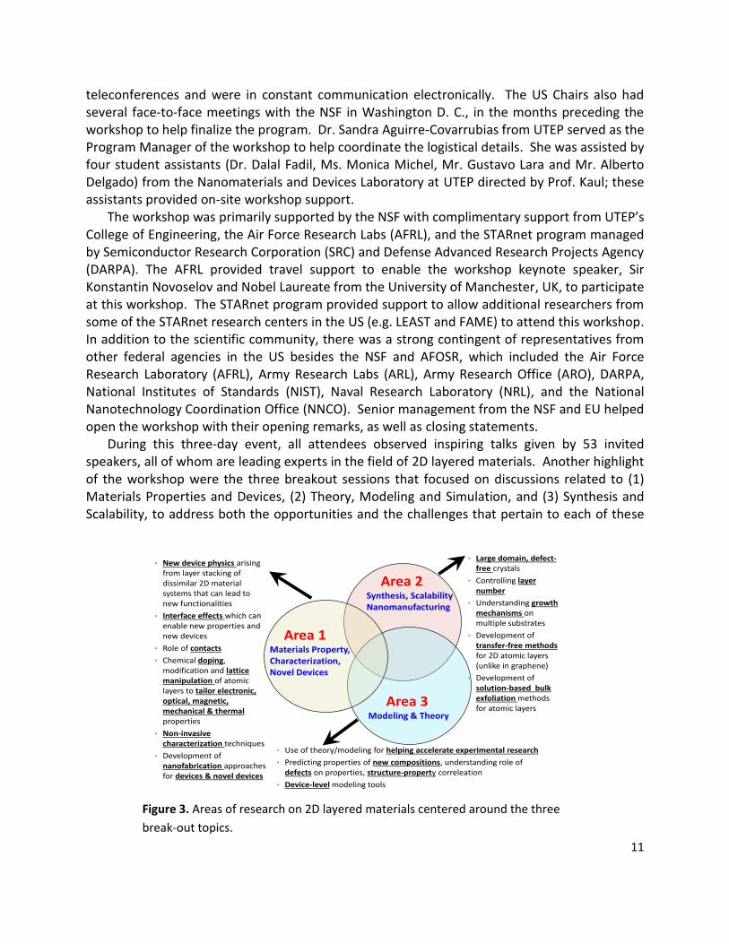
During this three-day event, all attendees observed inspiring talks given by 53 invited speakers, all of whom are leading experts in the field of 2D layered materials. Another highlight of the workshop were the three breakout sessions that focused on discussions related to (1) Materials Properties and Devices, (2) Theory, Modeling and Simulation, and (3) Synthesis and Scalability, to address both the opportunities and the challenges that pertain to each of these
Area 2Synthesis, ScalabilityNanomanufacturing
Area 1Materials Property,Characterization,Novel Devices
Area 3Modeling & Theory
• Large domain, defect-free crystals
• Controlling layer number
• Understanding growth mechanisms on multiple substrates
• Development of transfer-free methodsfor 2D atomic layers (unlike in graphene)
• Development of solution-based bulk exfoliation methods for atomic layers
• Use of theory/modeling for helping accelerate experimental research
• Predicting properties of new compositions, understanding role of defects on properties, structure-property correleation
• Device-level modeling tools
• New device physics arising from layer stacking of dissimilar 2D material systems that can lead to new functionalities
• Interface effects which can enable new properties and new devices
• Role of contacts
• Chemical doping, modification and lattice manipulation of atomic layers to tailor electronic, optical, magnetic, mechanical & thermal properties
• Non-invasive characterization techniques
• Development of nanofabrication approaches for devices & novel devices
Figure 3. Areas of research on 2D layered materials centered around the three
break-out topics.

12
topics. Figure 3 provides a summary of the broadly defined areas of exploration for the three topics.
The keynote presentation was given by Nobel Laureate, Sir Konstantin Novoselov from the UK, who highlighted the state-of-the-art in 2D layered materials research and the new mechanisms that can emerge from exploring 2D material heterostructures. The workshop closing talk provided by Professor Tony Heinz from Stanford University, also shed insights into the fundamental optical properties of 2D layered materials induced via quantum confinement effects.
Other highlights of the workshop included two working lunch speakers. Dr. Vladimir Falko provided the first working lunch talk to increase awareness of a new recently launched journal, The 2D Materials Journal from the Institute of Physics. On Day 2, Dr. Dennis P. Butcher Jr. described the US Department of Defense’s (DoD’s) International Programs. The two working dinner speakers included Dr. Mark Suskin from the NSF who spoke about NSF international programs, while Dr. Thomas N. Theis from IBM research discussed the device possibilities enabled by 2D materials. A panel discussion was also hosted on Day 2, composed of federal agency representatives from the US: Dimitris Pavlidis (NSF), Ken Goretta (AFOSR), Kiki Ikossi (DTRA), Pani Varanasi (ARO), Avram Bar-Cohen (DARPA), and Gernot Pomerenke (AFOSR); Jari Kinaret and Wide Hogenhout were also a part of this panel discussion to share perspectives from the EU-side. Two additional members who joined this panel discussion while at the workshop and who were not listed in the formal program, included Joe Qiu from ARO and Lisa Fridersdorf from the NNCO.
Through the technical discussions held at the workshop, another aim was to help open a dialogue between the EU (e.g. EU Commission) and US funding agencies (e.g. NSF) to discuss mechanisms that can help catalyze greater activity and collaborations between researchers in the two regions in this area of research. The website dedicated to this workshop (http://engineering.utep.edu/useu2dworkshop/) contains a wealth of information including a copy of many of the presentations, as well as the participant list. This report summarizes what transpired at the workshop from the technical talks and the break-out discussions, and we are truly grateful to all of the invited speakers, guests, and program directors who participated to make this workshop such a successful and memorable event.

13
3.0 Agenda and List of Topics
3.1. Workshop Agenda
NSF US – EU Workshop on 2D Layered Materials and Devices
Holiday Inn at Ballston April 22 – 24, 2015 Arlington, VA, USA
WEDNESDAY, April 22, 2015
7:00 - 8:00 AM Registration & Continental Breakfast
8:00 - 8:15 AM Welcome and Introductions
Assistant Director for Engineering Division Director for Electrical, Communications, and Cyber Systems (ECCS) Division Director of the Office for Emerging Frontiers in Research and Innovation (EFRI) Program Director, ECCS Division
Pramod Khargonekar, NSF Samir El-Ghazaly, NSF Sohi Rastegar, NSF Dimitris Pavlidis , NSF
8:15 – 8:45 AM Overview Anupama Kaul, US US Workshop Chair
8:45 – 9:00 AM EU Flagship Wide Hogenhout, EU EU Flagship Office
9:00 – 9:40 AM
KEYNOTE Speaker "Heterostructures from 2D Atomic Crystals"
Session Chair: James Hwang (US) Lehigh University Sir Konstantin Novoselov Nobel Laureate, EU University of Manchester United Kingdom
9:40 – 11:00 AM Session I 2D Electronic Materials Properties & Devices (I)
Session Chair: Kenneth Goretta (US) AFOSR

14
9:40 - 9:55 AM "Quantum Transport in 2D Atomic Layers" Jeanie Lau (US) University of California, Riverside
9:55 – 10:10 AM "Bandstructure Engineering in Bilayer Graphene with Large Displacement Fields"
Klaus Ensslin (EU) ETH Zurich, Switzerland
10:10 – 10:25 AM "Excitonic Behavior in MX2 Monolayers" Berry Jonker (US) Naval Research Lab (NRL)
10:25 – 10:40 AM "2D Materials: Prospects for Electronics" Luigi Colombo (US) Texas Instruments
10:40 – 11:00 AM Discussion
11:00 – 11:20 AM Coffee Break
11:20 – 12:20 PM Session II 2D Electronic Materials Properties & Devices (II)
Session Chair: Dimitris Pavlidis, NSF
11:20 – 11:35 AM "Layered Materials for Electronics" Grace Xing (US) Cornell University
11:35 – 11:50 AM "MoS2 and Dichalcogenide-Based Devices and Hybrid Heterostructures"
Andras Kis (EU) EPFL, Switzerland
11:50 – 12:05 AM
"Synthesis & Properties of van der Waals Solids"
Joshua Robinson (US) The Pennsylvania State University
12:05 – 12:20 PM Discussion
12:20 – 1:30 PM Working Lunch Speaker "IOP 2D Materials Journal"
Vladimir Falko Lancaster University
1:30 – 3:05 PM Session III 2D Optical Materials Properties & Devices (I)
Session Chair: Charles Ying, NSF
1:30 – 1:45 PM "Picosecond Optoelectronics of 2D Materials and Devices" Alexander Holleitner (EU) Technical University of Munich, Germany
1:45 – 2:00 PM "Photocurrent Studies of 2D Material Devices" David Cobden (US) University of Washington
2:00 – 2:15 PM "Three-Particle Charged Complexes in TMDC Optics" Vladimir Falko (EU) Lancaster University
2:15 – 2:30 PM "Bridging the Gap: Layered Black Phosphorus for Electronics and Optoelectronics"
Fengnian Xia (US) Yale University
2:30 – 2:45 PM "Valley Zeeman Effect of Free and Bound Excitons in WSe2" Ajit Srivastava (for A. Immoglu) (EU) ETH Zurich, Switzerland
2:45 – 3:05 PM Discussion
3:05 – 3:25 PM Coffee Break
3:25 – 5:00 PM Session IV Theory & Modeling
Session Chair: Gianluca Fiori (EU) University of Pisa
3:25 – 3:40 PM "From the First Principles: Defects in 2D, Variability and Electronic Consequences"
Boris Yakobson (US) Rice University
3:40 – 3:55 PM "From Band Structures to Devices in 2D Dichalcogenides"
Guido Burkard (EU) University of Konstanz, Germany
3:55 – 4:10 PM "Phase Change and Electromechanical Properties of 2D Materials"
Evan Reed (US) Stanford University

15
4:10 – 4:25 PM "Engineering Electron and Hole Wires in 2D Materials through Polar Discontinuities"
Marco Gibertini (for N. Marzari) (EU) EPFL, Switzerland
4:25 – 4:40 PM "Strain Engineering of Electronic Structure and Topological Order in 2D Materials and their Heterostructures"
Vivek Shenoy (US) The Pennsylvania State University
4:40 – 5:00 PM Discussion
5:00 – 5:40 PM Session V Elemental 2D Materials: Phosphorene and Silicene
Session Chair: Peide Ye (US) Purdue University
5:00 – 5:20 PM "Graphene's Synthetic Cousins: Silicene and Germanene" Guy Le Lay (EU) PIIM-CNRS at Aix-Marseille University, France
5:20 – 5:40 PM "Phosphorene: Can it be Effectively Passivated?" James Hwang (US) Lehigh University
5:40 – 6:25 PM
Session VI Poster Session
6:25 – 8:00 PM Working Dinner Speaker, “NSF International Programs” Mark Suskin, NSF
THURSDAY, April 23, 2015
7:00 – 8:00 AM Late Registration & Continental Breakfast
8:00 – 8:15 AM Day 2 Opening Remarks: "The Graphene Flagship"
Jari Kinaret (EU) EU Workshop Chair Chalmers University of Technology, Sweden
8:15 – 10:05 AM
Session I Advances in Synthesis Techniques: Vapor & Solution-based Techniques
Session Chair: Lincoln J. Lauhon (US) Northwestern University
8:15 – 8:30 AM "Phase Engineering in 2D TMDs" Manish Chhowalla (US) Rutgers University
8:30 – 8:45 AM "Exploring Pathways to Heterostacks of Graphene and Hexagonal Boron Nitride"
Juerg Osterwalder (EU) University of Zurich, Switzerland
8:45 – 9:00 AM "Hetero-Structures in 2D Systems: From Doped Monolayers to van der Waals Solids"
Mauricio Terrones (US) The Pennsylvania State University
9:00 – 9:15 AM "Liquid-Exfoliation of 2D Materials: From Fundamental Studies Towards Applications"
Claudia Backes (for J. Coleman) (EU) Trinity College, Ireland
9:15 – 9:30 AM "2D TMDC Materials: Engineering Light-Matter Interactions at The Atomic-Scale"
Linyou Cao (US) North Carolina State University
9:30 – 9:45 AM "Light-Matter Interaction in Superlattices and Heterostructures Made of 2D Crystals"
Cinzia Casiraghi (EU) University of Manchester, United Kingdom
9:45 – 10:05 AM Discussion
10:05 – 10:25 AM Coffee Break – Group Photo
10:25 – 11:45 AM Session II 2D Layered Materials: Sensors, Electronics, Energy, and Integration
Session Chair: Jeremy Robinson (US) Naval Research Lab

16
10:25 - 10:40 AM "Two-Dimensional Carbides and Nitrides of Transition Metals - the Largest Family of 2D Materials?"
Yuri Gogotsi (US) Drexel University
10:40 - 10:55 AM "Integration Challenges and Opportunities for 2D Materials"
Mark Hersam (US) Northwestern University
10:55 - 11:10 AM "Graphene and New 2D Materials: Opportunities for High Frequency Applications"
Henri Happy (EU) IEMN, France
11:10 - 11:25 AM "Integrating 2D Materials in Planar Photonic Circuits for Optical Communication"
Mo Li (US) University of Minnesota
11:25 – 11:45 AM Discussion
11:45 – 1:00 PM Working Lunch Speaker "DOD International Programs"
Dennis P. Butcher Jr. AFSOR
1:00 – 2:50 PM Session III Breakout Sessions (Parallel Sessions)
Topic 1 – Ballroom Materials Properties and Device Research: Core Challenges to Address in 2 D Materials Property Characterization, Device Research in Photonics, Energy, Flexible Electronics, Sensors.
Breakout Chairs: EU: Andras Kis US: Grace Xing Scribe: Jeanie Lau
Topic 2 – Fairfax Theory, Modeling and Simulation: Modeling, Characterization, Materials Property Database, Status of US Materials Genome Initiative.
Breakout Chairs: EU: Guido Burkard US: Vivek Shenoy Scribe: Evan Reed
Topic 3 – Wilson Synthesis and Scalability: Synthesis and Scalability for Translational Opportunities and Roadmap for Low End and High End Applications.
Breakout Chairs: EU: Juerg Osterwalder US: Manish Chhowalla Scribe: Mauricio Terrones
2:50 – 3:05 PM Coffee Break
3:05 – 4:20 PM Session IV 2D Electronic Materials Properties & Devices (III)
Session Chair: Dr. Pani Varanasi (US) Army Research Office
3:05 – 3:20 PM "Electron Transport in the van der Waals Interfaces" Philip Kim (US) Harvard University
3:20 – 3:35 PM "2D Crystals for Nanoelectronics and Beyond" Kaustav Banerjee (US) University of California, Santa Barbara
3:35 – 3:50 PM "Spectral Response of 2D Material-Based Photodiodes" Max Lemme (EU) University of Siegen, Germany
3:50 – 4:05 PM "High-Field, Thermal and Energy Properties of 2D Devices and Layers"
Eric Pop (US) Stanford University
4:05 – 4:20 PM Discussion
4:20 – 5:35 PM Session V Electronics & Novel Materials: Phosphorene, Silicene, Germanene, etc.
Session Chair: Fengnian Xia (US) Yale University
4:20 – 4:35 PM "Black Phosphorus and Phosphorene for Device Applications"
Peide Ye (US) Purdue University
4:35 – 4:50 PM "Group IV Graphene Analogues" Joshua Goldberger (US) Ohio State University

17
4:50 – 5:05 PM "Challenges and Opportunities of 2D Materials for Electronic Applications"
Gianluca Fiori (EU) University of Pisa, Italy
5:05 – 5:20 PM
"Buckled Atomic Sheets: The Intriguingly Complex Case of Phosphorene and Silicene"
Deji Akinwande (US) University of Texas at Austin
5:20 – 5:35 PM "Graphene Photonics and Optoelectronics" Andrea Ferrari (EU) University of Cambridge, United Kingdom
5:35 – 5:50 PM Discussion
5:50 – 6:35 PM Session VI Panel Discussion Panel on Research Programs on 2D Layered Materials
Moderator: Luigi Colombo (US) Texas Instruments
(2 to 3 Minute Overview by Each Program and then Open for Panel Discussion)
EU Graphene Flagship Jari Kinaret (EU)
NSF EFRI 2DARE Dimitris Pavlidis (US)
AFOSR BRI Ken Goretta (US)
EU Graphene Flagship Wide Hogenhout (EU)
ARO MURI Pani Varanasi (US)
DTRA Kiki Ikossi (US)
DARPA Avram Bar-Cohen (US)
AFOSR Gernot Pomrenke (US)
7:20 – 8:30 PM Working Dinner Speaker "Post-CMOS Device Concepts Enabled by 2D Materials"
Thomas N. Theis IBM Research
FRIDAY, April 24, 2015
7:00 – 8:00 AM Continental Breakfast
8:00 – 9:05 AM Session I 2D Optical Materials Properties & Devices (II)
Session Chair: David H. Cobden (US) University of Washington
8:00 – 8:15 AM "Single Photon Emitters in Exfoliated WSe2 Structures" Marek Potemski (EU) LNCMI-CNRS, France
8:15 – 8:30 AM "Optoelectronics of 2D Semiconductors and Heterostructures"
Xiaodong Xu (US) University of Washington
8:30 – 8:45 AM "Tunable Half-light Half-matter Polaritons in van der Waals Heterostructures"
Alexander Tartakovski (EU) University of Sheffield, United Kingdom
8:45 – 9:05 AM Discussion
9:05 – 10:50 AM
Session II Breakout Presentations Presentation and Discussion of Breakout Sessions to Entire Group
(35 Minutes for Each Breakout: 20 Minutes Presentation & 15 Minutes Discussion)
9:05 – 9:40 AM Topic 1 Materials Properties & Device Research
US EU Breakout Chairs
9:40 – 10:15 AM Topic 2 Theory, Modeling and Simulation
US EU Breakout Chairs
10:15 – 10:50 AM Topic 3 Synthesis and Scalability
US EU Breakout Chairs
10:50 – 11:10 AM Coffee Break

18
11:10 – 11:50 AM
Closing Talk "Probing Electronic Properties of Atomically Thin Transition Metal Dichalcogenide Layers and Heterostructures"
Session Chair: Anupama Kaul (US) University of Texas, El Paso Tony Heinz (US) Stanford University
11:50 – 12:00 PM Summary & Adjournment Anupama Kaul (US-Chair) Jari Kinaret (EU-Chair) Dimitris Pavlidis (NSF)
Lunch on Your Own
3.2. List of Topics
The list of topics discussed at this workshop is provided below. The talks ranged from elucidating the unique properties of 2D layered materials, developing novel material characterization schemes, device nanofabrication, device design and characterization, theory and modeling for predicting properties and device performance, and synthesis techniques for potential scalability.
Materials Properties and Devices:
i. Optoelectronics of 2D materials: Optical properties of monolayers and multilayers of TMDCs, phosphorene, van der Waals hetero- and superstructures, spin and valley effects, properties of excitons and charged complexes, and photonic devices and circuits.
ii. Electronic transport properties: New generation of high-mobility van der Waals solids such as some of the TMDCs and phosphorene, heterostructures, exploring transport properties and the role of strain, substrate choices, and contacts on such properties.
iii. Device Applications: Beyond-CMOS devices, novel tunneling devices enabled by heterostructures, flexible electronics, sensors, energy harnessing and energy storage devices, and catalysis.
Theory and Modeling: This topic focused on looking at theory and predictive modeling to understand materials and device properties, as well as predicting new structures and materials systems to gather insights into structure-property correlations, understanding the role of defects, excitonic physics, and predicting strain-related effects in 2D layered materials.
Synthesis and Nanomanufacturing: This topic discussed solution-based exfoliation methods for large-scale integration of 2D layered materials, vapor-based synthesis techniques, characterizing the role of defects for synthesis of TMDCs, nitrides, and elemental layered materials (e.g. silicene, phosphorene), among others.

19
3.3. List of Participants
No First Name Last Name Organization E-Mail 1 Sandra Covarrubias University of Texas at El Paso [email protected]
2 Deji Akinwande University of Texas at Austin [email protected]
3 Claudia Backes Trinity College Dublin [email protected]
4 Kaustav Banerjee University of California, Santa Barbara [email protected]
5 Avram Bar-Cohen DARPA [email protected]
6 Ludwig Bartels University of California at Riverside [email protected]
7 Guido Burkard University of Konstanz [email protected]
8 Dennis Butcher Jr AFOSR IO [email protected]
9 Linyou Cao NC State University [email protected]
10 Cinzia Casiraghi University of Manchester [email protected]
11 Roman Caudillo Intel Corporation [email protected]
12 Phillip Chang DARPA MTO [email protected]
13 Michael Check AFRL [email protected]
14 Manish Chhowalla Rutgers University [email protected]
15 Kyeongjae Cho University of Texas, Dallas [email protected]
16 David Cobden University of Washington [email protected]
17 Luigi Colombo Texas Instruments [email protected]
18 Albert Davydov National Institute of Standards (NIST) [email protected]
19 Alberto Delgado University of Texas at El Paso [email protected]
20 Xlangfeng Duan University of California, Los Angeles [email protected]
21 Madan Dubey US Army Research Lab [email protected]
22 Samir El-Ghazaly National Science Foundation [email protected]
23 Nadia El Masry National Science Foundation [email protected]
24 Klaus Ensslin ETH Zurich [email protected]
25 Dalal Fadil University of Texas at El Paso [email protected]
26 Vladimir Falko Lancaster University [email protected]
27 Randall Feenstra Carnegie Mellon University [email protected]
28 Jonathan Felbinger DoD [email protected]
29 Andrea Ferrari University of Cambridge [email protected]
30 Gianluca Fiori University of Pisa [email protected]
31 Susan Fullerton University of Notre Dame [email protected]
32 Mary Galvin DMR, NSF [email protected]
33 Sabyasachi Ganguli AFRL [email protected]
34 Marco Gibertini EPFL [email protected]
35 Yury Gogotsi Drexel University [email protected]
36 Joshua Goldberger Ohio State University [email protected]
37 Ken Goretta AFOSR [email protected]
38 Henri Happy University of Lille 1 - IEMN [email protected]
39 Tony Heinz Stanford University [email protected]
40 Mark Hersam Northwestern University [email protected]
41 Wide Hogenhout European Commission [email protected]
42 Alexander Holleitner Technical University Munich [email protected]

20
43 Yu Huang University of California, Los Angeles [email protected]
44 James Hwang Lehigh University [email protected]
45 Kiki Ikossi Defense Threat Reduction Agency (DTRA) [email protected]
46 Tony Ivanov US Army Research Laboratory [email protected]
47 Berry Jonker Naval Research Laboratory [email protected]
48 Anupama Kaul University of Texas at El Paso [email protected]
49 Roland Kawakami Ohio State University [email protected]
50 Jeffry Kelber University of North Texas [email protected]
51 Pramod Khargonekar National Science Foundation [email protected]
52 Philip Kim Harvard University [email protected]
53 Ki Wook Kim North Carolina State University [email protected]
54 Jari Kinaret Chalmers University of Technology, Applied Physics [email protected]
55 Andras Kis Ecole Polytechnique Federale de Lausanne (EPFL) [email protected]
56 Steven Koester University of Minnesota [email protected]
57 Zoran Krivokapic Global Foundaries [email protected]
58 Tillmann Kubis Purdue University [email protected]
59 Maija Kukla National Science Foundation [email protected]
60 Roger Lake University of California Riverside [email protected]
61 Gustavo Lara University of Texas at El Paso [email protected]
62 Jeanie Lau University of California, Riverside [email protected]
63 Lincoln Lauhon Northwestern University [email protected]
64 Guy Le Lay Aix-Marseille University [email protected]
65 Max Lemme University of Siegen [email protected]
66 Mo Li University of Minnesota [email protected]
67 Monica Lugo University of Texas at El Paso [email protected]
68 Michael McConney AFRL [email protected]
69 Shin Mou Air Force Research Lab [email protected]
70 Konstantine Novoselov University of Manchester [email protected]
71 Juerg Osterwalder University of Zurich, Switzerland [email protected]
72 Shanee Pacley AFRL [email protected]
73 Tim Patten National Science Foundation [email protected]
74 Dimitris Pavlidis National Science Foundation [email protected]
75 Gernot Pomrenke AFOSR [email protected]
76 Eric Pop Stanford University [email protected]
77 Marek Potemski CNRS-UJF-UPS-INSA [email protected]
78 Joe Qiu Army Research Office [email protected]
79 Daniel Radack IDA [email protected]
80 Sohi Rastegar National Science Foundation [email protected]
81 Joan Redwing Pennsylvania State University [email protected]
82 Evan Reed Stanford University [email protected]
83 Joshua Robinson Pennsylvania State University [email protected]

21
84 Jeremy Robinson Naval Research Laboratory [email protected]
85 Mike Roco National Science Foundation [email protected]
86 Mike Scott National Science Foundation [email protected]
87 Alan Seabaugh University of Notre Dame [email protected]
88 Vivek Shenoy Pennsylvania State University [email protected]
89 Uttam Singisetti University at Buffalo SUNY [email protected]
90 Paul Sokol DMR [email protected]
91 Ajit Srivastava ETH Zurich [email protected]
92 Mark Suskin National Science Foundation [email protected]
93 Alexander Tartakovskii University of Sheffield [email protected]
94 Humberto Terrones Rensselaer Polytechnic Institute [email protected]
95 Mauricio Terrones Pennsylvania State University [email protected]
96 Thomas Theis SRC-NRI [email protected]
97 Abbas Torabi Raytheon [email protected]
98 Gilroy Vandentop Semiconductor Research Corporation [email protected]
99 Pani Varanasi Army Research Office [email protected]
100 Andrey Voevodin Air Force Research Laboratory [email protected]
101 Eric Vogel Georgia Institute of Technology [email protected]
102 Robert Wallace University of Texas at Dallas [email protected]
103 Haiyan Wang Division of Materials Research [email protected]
104 Fengnian Xia Yale University [email protected]
105 Ya Hong Xie UCLA, Materials Science & Engineering Dept [email protected]
106 Grace Xing Cornell University [email protected]
107 Xiaodong Xu University of Washington [email protected]
108 Boris Yakobson Rice University [email protected]
109 Peide Ye Purdue University [email protected]
110 Charles Ying National Science Foundation [email protected]
111 Mona Zaghloul National Science Foundation [email protected]
22
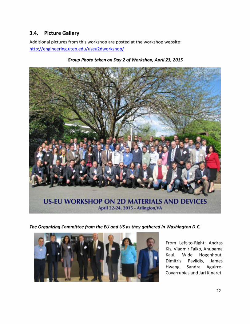
3.4. Picture Gallery
Additional pictures from this workshop are posted at the workshop website:
http://engineering.utep.edu/useu2dworkshop/
Group Photo taken on Day 2 of Workshop, April 23, 2015
The Organizing Committee from the EU and US as they gathered in Washington D.C.
From Left-to-Right: Andras Kis, Vladmir Falko, Anupama Kaul, Wide Hogenhout, Dimitris Pavlidis, James Hwang, Sandra Aguirre-Covarrubias and Jari Kinaret.

23
Speakers and Guests
4.0 Technical Highlights and Break-out Summaries
Technical highlights are presented in this section that revolve around the three breakout session topics, specifically, 1) Materials Properties and Devices, 2) Theory, Modeling and Simulation, and 3) Synthesis and Scalability, which are presented in Sections 4.1, 4.2, and 4.3, respectively. The technical highlights for each of the three topics are summarized in Sections 4.1.1, 4.2.1, and 4.3.1, while the respective break out reports follow these in Sections 4.1.2, 4.2.2, and 4.3.2, respectively.
The break-out reports were compiled by the break out session leaders for each of the three topics. The breakout sessions drew very enthusiastic participation from all of the workshop attendees. To facilitate and help guide the break out discussions, the organizing committee came

24
up with a list of potential questions which were provided to the breakout leaders weeks prior to the workshop to help them prepare for these discussions. These guiding questions were divided into two categories, A. General and Programmatic Considerations, and B. Topic-specific Questions, and are reproduced here.
A. General and Programmatic Questions:
Current State of Field
1. Current state-of-the-field with respect to the specific break out topic (i.e. topics 1 through 3). Some examples of topic-specific questions have been provided in Section B below.
2. Can a roadmap for the topic/field be proposed or is it too early? i. What are the key areas where 2D materials and devices are expected to (a) make a
substantial difference with respect to existing technologies; (b) the industry is primarily interested in and the research community can help guide research towards the interests and needs of industry?
Potential Challenges & Obstacles 1. What are the key areas in which knowledge and resources limit the progress of this field,
as perceived by US and EU researchers, which may prevent us from reaching the desired goals? i. Can a collaboration help overcome these hurdles?
2. What is needed in the research infrastructure to transform the promise of this field to an area of scientific and technological strength?
3. What lessons can we learn from prior research “waves” that will help speed-up R&D of 2D layered materials and devices?
How Can EU-US Collaboration Help Address Challenges? 1. How do you envision a US EU collaboration will help accelerate research for the topic and
what are some of the avenues you foresee as being valuable, such as bi-lateral exchange programs at all levels (faculty, postdocs, students), shared facilities, etc.?
2. Are there specific areas within each break out topic that should get priority for US-EU collaboration? Why?
3. What are the objectives to be achieved within those topics? 4. How can the progress made through EU-US collaboration be measured?
B. Topic-specific Questions:
Topic 1 - Materials Properties and Device Research: 1. Core challenges to address in 2D materials property characterization? 2. New characterization tools & approaches? 3. Integration of materials to devices, role of contacts, doping, substrates, etc. 4. Device challenges & opportunities in electronics, photonics, energy, flexible
electronics, sensors etc.?

25
5. Which devices and components will 2D materials and devices outperform and replace among currently existing approaches: (a) active devices; (b) passive components/applications; (c) other?
Topic 2 - Theory, Modeling and Simulation: 1. Modeling tools & techniques and the prospect of a materials property database? 2. Status of the US Materials Genome Initiative (MGI) and the US nanotechnology
knowledge infrastructure (NKI) signature initiative. Topic 3 - Synthesis and Scalability:
1. Synthesis and scalability for translational opportunities. 2. What are the needs and potential barriers in global manufacturing of 2D based
materials and devices? 3. Roadmap for low-end and high-end applications, engagement with industry and
equipment manufacturers for scalability?
The first of these topics, “Materials Properties and Devices,” is now discussed in Section 4.1, which starts with the technical highlights gathered in Section 4.1.1, and then the break out summary for this topic is presented in Section 4.1.2.
4.1. Materials Properties and Devices Summary 4.1.1. Technical Highlights Discussion related to “Materials Properties and Devices” spanned the entire three days of the workshop. Specifically, these included Sessions I, II, III, V on Day 1; Sessions II, IV and IV on Day 2; and Session I on Day 3. Being the most widespread topic, this overarching area is further categorized into six areas of high activity which includes: a) Optical Properties; b) Optical Material Characterization Techniques; c) Electronic, Thermal and Related Properties; d) Heterostructures; e) Devices and Applications; and f) Emergent 2D Layered Materials (e.g. silicene and phosphorene).
The keynote opening presentation by Sir Konstantin Novoselov from Manchester University, as well as the closing talk by Professor Tony Heinz from Stanford University, reviewed the fundamental materials properties of these 2D material systems and the potential device applications they enable. The keynote presentation by Sir Konstantin Novoselov elucidated the power of layer-by-layer engineering in forming heterostructures of MoS2, WS2, graphane, flurographene, BN, and graphene. These vertical heterostructures have already been shown to be promising for tunneling devices, such as tunneling transistors which exhibit ON/OFF ratios greater than 106 and are more than adequate for modern electronics.41,42 Tunneling structures were also discussed in the context of photodiodes and solar cells which exhibited large quantum efficiencies.43 Sir Novoselov also provided a detailed discussion related to tunneling structures showing large peak-to-valley gate-tunable currents, which also exhibit negative differential conductance. Momentum conservation was discussed in such structures where the conical cross sections also introduce additional conservation restrictions.44,45 Sir Novoselov also presented

26
promising examples of 2D materials integrated onto flexible and transparent substrates;42,46 flexible electronics is an area considered by many to be one of the more nearer term applications for 2D layered materials.
In his closing talk, Professor Tony Heinz presented his recent work that shed insights into explaining the optical properties of monolayers of TMDCs, such as MoS2, MoSe2, MoTe2, WS2, WSe2. He recapped his group’s prior work that showed the transition of 2D MoS2 from being an indirect-gap material in the bulk, to a direct-gap semiconductor for monolayers.34 Two types of interactions in these 2D TMDC materials were discussed. The first focused on the many-body interaction between charge carriers in one layer, and the second was targeted at interactions that occur in bilayers. Spectroscopic studies were conducted that reveal the progression of excited exciton states through precise absorption measurements which yielded exciton binding energies of several hundred meV. Another unusual type of interaction associated with these materials concerns the electronic states and transitions expected in stacks of TMDC monolayers with adjustable twist angle between the crystal planes of the layers.
Both of these opening and closing talks revealed the importance of basic science and discovery in enhancing our understanding of the fundamental properties of 2D layered materials, and the ensuing possibilities for furthering device research. The technical highlights of the rest of the talks that spanned the topic of 2D Materials Properties and Devices are now discussed below in the context of the six areas mentioned earlier, specifically: a) Optical Properties; b) Optical Material Characterization Techniques; c) Electronic, Thermal and Related Properties; d) Heterostructures; e) Devices and Applications; and f) Emergent 2D Layered Materials (e.g. silicene and phosphorene).
a) Optical Properties: Many of the talks at the workshop focused on the optical properties of 2D layered materials, in particular the TMDCs. In TMDCs the d-orbital conductivity of the metallic components makes them an interesting material system for exploring optical properties. Quantum confinement effects in 2D layered materials turn some of these materials, such as MoS2, WS2, WSe2, MoSe2 and MoTe2, from indirect-band gap semiconductors to direct band gap semiconductors in going from the bulk to monolayers.34,47 Besides the observed band gap transition from indirect-to-direct gap, it is also interesting to note that the band gaps in some bilayer TMDCs can be tuned through the application of an external electric field. For example, density functional theory calculations conducted on bilayer MoS2, WS2, MoSe2, and MoTe2 show that that their band gaps undergo a gradual semiconducting-to-metallic transition through the application of an external electric field oriented orthogonal to the plane of the layers.48 The optical properties of 2D layered materials can enable photodetection, for example in mechanically exfoliated layers of MoS2, where the photocurrent was shown to depend on the incident light intensity.49 In addition, by using MoS2 layers of different thicknesses, photo-detection can be tuned for different wavelengths where single- and double-layer MoS2 were shown to be effective for detecting green light, while triple-layer MoS2 was well suited for red light.50 Given the tunable, direct band gaps of some of the 2D TMDCs and their relative earth abundance, they also appear to be a promising choice for solar cells, potentially opening up prospects for multi-junction solar cells that capture photons from the visible to the near-infrared.51 Recent work has also shown

27
that layers as thin as 1 nm of materials such as MoS2, MoSe2, and WS2, have the exceptional ability to absorb 5–10% of the incident light.52 When compared to conventional solar cell materials such as GaAs and Si, the absorption in some of these 2D layered materials is an order of magnitude higher.
A significant fraction of the talks at the workshop discussed excitonic effects in 2D layered materials. The reduced screening in 2D layered materials results in enhanced electron-electron interactions which are largely responsible for the excitonic effects, as well as the large excitonic binding energies that seem to be characteristic of 2D semiconducting TMDCs. Well known scientists at this workshop who presented their work in exploring the optical properties of 2D layered materials included: Berry Jonker, Vladimir Falko, Ajit Srivastava, Linyou Cao, Andrea Ferrari, Xiaodong Xu, and Alexander Tartakovskii.
Berry Jonker described his team’s work on measuring the excitonic binding energy of WS2 and WSe2 monolayers, where measurements were conducted over a wide range of temperatures from 4K to 300 K. Vladimir Falko has examined three-particle charged complexes in TMDCs and compared binding energies of trions X±, with that of localized charged complexes.53 His analysis suggests that the disassociation energy of X± is significantly larger than those of localized exciton complexes, implying that trions are more resilient to heating as compared to defect-localized excitons. Ajit Srivastava, who represented Atac Imamoglu’s group at EPFL, has studied the valley Zeeman effect of free and bound excitons in WSe2, where the pseudo-spin degree of freedom in WSe2 can be optically addressed using circularly polarized light.54 Low temperature magneto-optical spectroscopy was utilized in this work to investigate the exciton and trion resonance in the presence of magnetic fields. Their results show that the valley degree of freedom is preserved even in bound excitons, making them attractive for optical control of spin-valley degree of freedom in TMDCs.55
In work conducted by Linyou Cao, analysis of the dielectric function of atomically thin MoS2
was conducted as a function of layer number. Cao has found that the dielectric function shows an anomalous dependence on the layer number; it first decreases and then increases as the layer number increases beyond five layers. He has attributed the decrease in the dielectric function to the contribution of excitons to the dielectric function. Andrea Ferrari presented a review of 2D materials for photonics and optoelectronics applications, touching upon topics such as their use in optical absorbers, photodetectors, plasmonics, in addition to discussing other areas such as spintronics of 2D materials and their use in sensors and flexible electronics.56
Xiaodong Xu discussed his group’s work to demonstrate the valley-specific interlayer excitons in monolayer WSe2-MoSe2 vertical heterostructures through optical pumping. Coupled spin-valley polarization of interlayer excitons was conducted and polarization lifetimes were measured to be more than 10 nanoseconds. Alexander Tartakovskii discussed the ability to tune exciton-polaritons in van der Waals heterostructures of MoSe2 and h-BN through the construction of van der Waals quantum wells. He has observed the strong exciton-photon coupling regime and formation of exciton-polariton states, whose energy can be tuned by changing the gap between the distributed Bragg reflector mirrors.57

28
b) Optical Material Characterization Techniques: Several talks at the workshop were focused on utilizing novel optical characterization schemes that will provide researchers with the techniques necessary to allow deeper insights into some of the optoelectronic properties of 2D layered materials. Talks related to novel optical characterization schemes were provided by Alexander Holleitner, David Cobden, and Marek Potemski. Alexander Holleitner discussed his work in characterizing picosecond transport dynamics of photogenerated charge carriers in 2D materials using an on-chip pump/probe scheme to measure the photocurrent dynamics which conventional electronic measurements fail to capture directly.58 His group has isolated the non-radiative energy transfer from fluorescent emitters, specifically nitrogen vacancy centers, in graphene59 which are likely to pave the way for future quantum devices.60
David Cobden discussed his work on photocurrent microscopy where the short-circuit current generated by a 2D layered material sample is measured when a laser is focused at a point or scanned over it. Cobden has found that when a perpendicular magnetic field is applied, an additional photocurrent is generated near the sample edges, other than what is observed near contacts, junctions and in homogeneities. He has explained this behavior on the basis of the photo-Nernst effect, where a current density is induced perpendicular to the laser-induced temperature gradient. Marek Potemski discussed optical micro-spectroscopy studies of thin layers of WSe2, where the edges of WSe2 flakes give rise to sharp emission lines down to 0.1 meV at low temperatures. These narrow emission lines reveal the effect of photon ant bunching, a direct signature of single photon emitters.
c) Electronic, Thermal and Related Properties: The scaling trends of Si transistors according to Moore’s Law has integrated nearly billions of transistors into smaller and smaller areas, as illustrated in Fig. 4, which poses a serious concern in mitigating heat management issues. Through phonon engineering in the atomically sharp interfaces of 2D materials, thermal transport across interfaces can be tuned and optimized, which
will play a major role in determining the performance of ultra-high-density nanoscale circuits. Several talks scattered through the three days of the workshop were focused on a discussion of the electronic and thermal properties of 2D layered materials,
which included researchers Jeanie Lau, Klaus Ensslin, Grace Xing and Eric Pop.
In her talk, Jeanie Lau discussed quantum transport in graphene and the results of dual-gated suspended ABC trilayer graphene structures. She also discussed quantum transport and mobility of suspended and unsuspended MoS2 and considered the effects of contacts on the transport characteristics, along with her current research activities in few-layer phosphorene structures for high-mobility devices. Klaus Ensslin has studied the effect of large vertical electric fields in bilayer graphene which opens a band gap in graphene as discussed during his talk. Grace Xing talked
Figure 4. Moore’s Law scaling trends showing number of transistors on a chip, which has now exceeded 1 billion.
29
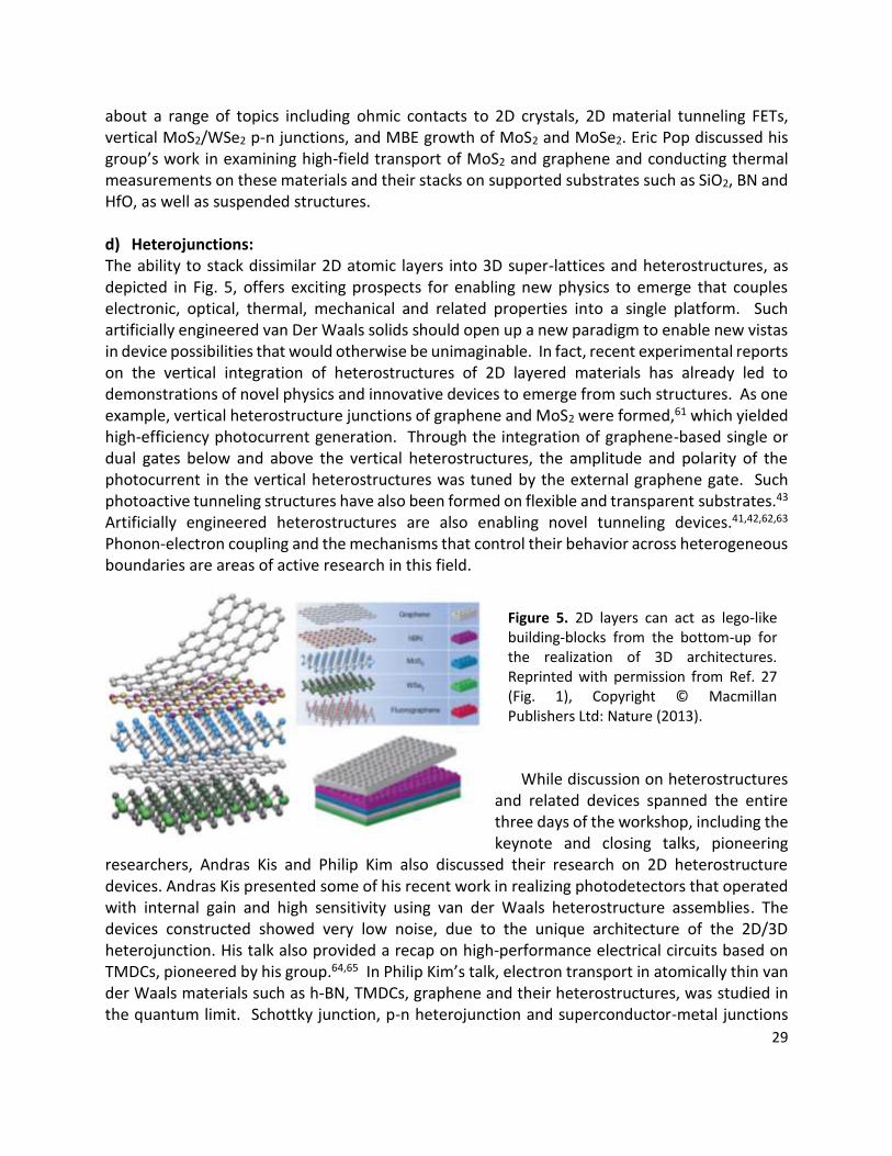
about a range of topics including ohmic contacts to 2D crystals, 2D material tunneling FETs, vertical MoS2/WSe2 p-n junctions, and MBE growth of MoS2 and MoSe2. Eric Pop discussed his group’s work in examining high-field transport of MoS2 and graphene and conducting thermal measurements on these materials and their stacks on supported substrates such as SiO2, BN and HfO, as well as suspended structures. d) Heterojunctions: The ability to stack dissimilar 2D atomic layers into 3D super-lattices and heterostructures, as depicted in Fig. 5, offers exciting prospects for enabling new physics to emerge that couples electronic, optical, thermal, mechanical and related properties into a single platform. Such artificially engineered van Der Waals solids should open up a new paradigm to enable new vistas in device possibilities that would otherwise be unimaginable. In fact, recent experimental reports on the vertical integration of heterostructures of 2D layered materials has already led to demonstrations of novel physics and innovative devices to emerge from such structures. As one example, vertical heterostructure junctions of graphene and MoS2 were formed,61 which yielded high-efficiency photocurrent generation. Through the integration of graphene-based single or dual gates below and above the vertical heterostructures, the amplitude and polarity of the photocurrent in the vertical heterostructures was tuned by the external graphene gate. Such photoactive tunneling structures have also been formed on flexible and transparent substrates.43 Artificially engineered heterostructures are also enabling novel tunneling devices.41,42,62,63 Phonon-electron coupling and the mechanisms that control their behavior across heterogeneous boundaries are areas of active research in this field.
While discussion on heterostructures
and related devices spanned the entire three days of the workshop, including the keynote and closing talks, pioneering
researchers, Andras Kis and Philip Kim also discussed their research on 2D heterostructure devices. Andras Kis presented some of his recent work in realizing photodetectors that operated with internal gain and high sensitivity using van der Waals heterostructure assemblies. The devices constructed showed very low noise, due to the unique architecture of the 2D/3D heterojunction. His talk also provided a recap on high-performance electrical circuits based on TMDCs, pioneered by his group.64,65 In Philip Kim’s talk, electron transport in atomically thin van der Waals materials such as h-BN, TMDCs, graphene and their heterostructures, was studied in the quantum limit. Schottky junction, p-n heterojunction and superconductor-metal junctions
Figure 5. 2D layers can act as lego-like building-blocks from the bottom-up for the realization of 3D architectures. Reprinted with permission from Ref. 27 (Fig. 1), Copyright © Macmillan Publishers Ltd: Nature (2013).
30
have been realized by his group, to potentially enable efficient, fast and tunable bipolar electronics. Philip Kim has also observed a modulation of the Andreev reflection probability when Cooper pairs are injected across a van der Waals interface, specifically between a superconductor and graphene. e) Devices and Applications As eluded to earlier, 2D layered materials and their heterostructures can enable novel devices for nanoelectronics applications. Earlier work on h-BN and MoS2 vertical heterostructure FETs demonstrated tunneling currents in such devices.41 The tunneling time for electrons to traverse the nanometer-thick barrier was demonstrated to be extremely small in the range of femtoseconds, which far exceeds the switching frequency of conventional planar FETs and provides a promising example for the potential of 2D heterostructures for beyond-CMOS architectures. Important factors for the transistor applications of 2D materials are issues such as the ability to control doping of the semiconducting layered materials to selectively form p- and n-type regions for realizing 2D complimentary logic circuits.66 Besides selectively doping n-type and p-type regions in the same parent semiconductor, forming lateral heterostructures of dissimilar materials, similar to recent work with graphene67 and h-BN,68 suggests prospects for realizing 2D lateral n-type and p-type heterostructures. The issues to be resolved include identifying the appropriate substrates where both the n-type (e.g. MoS2) or p-type (e.g. WSe2) semiconductors can be synthesized laterally or as vertical heterostructures. For device and circuit applications, dielectrics are also necessary. Materials such as h-BN are attractive candidates for atomically-thin dielectrics, allowing for the design of various device architectures with metal/dielectric/semiconductor interfaces. Heterostructure FETs69 or tunneling devices70 formed by stacking 2D semiconductors as the channel, 2D insulator layers as the dielectric, and 2D metallic layers (graphene, TaSe2, etc.) as gates and interconnects can enable energy-efficient transistor devices71,72 for digital and analog circuit applications.73,74 Beyond single devices, multiple transistor devices have also been integrated to enable digital circuits, such as inverters and NOR logic gates by patterning electrodes on a single layer of MoS2 on which the circuits are fabricated.65 Recently complex integrated circuits built on bilayer MoS2 were also demonstrated which included an inverter circuit and a logic NAND gate to achieve static random access memory (SRAM) operation.75 Together with graphene and insulating materials such as h-BN, 2D semiconducting materials may be an attractive choice for constructing digital circuits on flexible and transparent substrates, as illustrated in Fig. 6, for applications such as paper-like transparent displays, wearable electronics and solar cells. In addition, the mechanical properties of MoS2 also appear to be very attractive given the strong intra-layer covalent bonds; the in-plane strength of MoS2 has been found to be 30 times larger than steel, where a Young’s Modulus of 270 GPa was measured. Leading researchers who presented their work on the device applications of 2D layered materials included: Luigi Colombo, Henry Happy, Kaustav Banerjee, Max Lemme, Gianluca Fiori, and Mo Li. Luigi Colombo provided a review of 2D TMDCs that will make them attractive for electronics from an industrial standpoint. Luigi Colombo also provided some perspectives on TMDCs and the difficulties in the preparation of low-defect-density, large-area, single crystals

31
using vapor transport, CVD, and molecular beam epitaxy. Henry Happy discussed the prospects for graphene field effect transistors (GFETs) where one of the focus areas is to increase fmax, the
frequency of oscillation, despite the fact that such GFETs have exhibited high gain cut-off frequency (ft) over 400 GHz. Kaustav Banerjee talked about his group’s progress in using 2D TMDCs in designing low-power, low-loss, and ultra energy-efficient active and passive devices for green electronics. Max Lemme described his work on measuring the spectral response of graphene/silicon and molybdenum diselenide (MoSe2)/silicon diodes.76 Additional discussion on the integration issues of graphene with other 2D materials was also presented, along with reliability issues of graphene FETs.77,78 Gianluca Fiori shared his perspectives, as gauged through theory and simulations, on the challenges of integrating 2D materials with conventional electronics for both digital and analog applications. Mo Li discussed approaches for integrating 2D materials, specifically black phosphorus with few layer graphene as the top cladding, into planar photonic circuits for optical communication. He discussed the responsivity and internal quantum efficiency of the black phosphorus devices and presented a framework for integrating these structures with
silicon photonics and CMOS circuitry.
f) Emergent 2D Layered Materials (e.g. Silicene and Phosphorene)
While research on 2D layered materials such as the TMDCs continues at a rapid pace, recently activities on elemental 2D layered materials besides graphene, are spawning new avenues for exploration. This includes interest in materials such as black phosphorus and silicene.79 Just like graphite, black phosphorus exhibits a layered structure, but unlike graphite it is a direct band gap semiconductor; mobilities as high as 10,000 cm2/V-s, have been reported, opening up prospects for its use in nanoelectronics, optoelectronics and sensors.80,81 Moreover, black phosphorus has a band gap of 0.3 eV in the bulk and by reducing thickness, the band gap can be tuned to be close to 2 eV for single atomic layers of black phosphorus known as phosphorene.82 Other exciting developments in elemental 2D materials includes research on 2D silicon or silicene. Planar 2D silicon appears unstable and reports show that a buckled morphology seems to be energetically more favorable for the realization of 2D silicene. Driven by the success of graphene research, interest in silicene, phosphorene and other elemental 2D materials continues to grow, which will help accelerate the integration of these exciting materials into practical devices.
At this workshop, there were half a dozen talks focused on such emergent 2D layered materials provided by Fengnian Xia, Guy Le Lay, James Hwang, Peide Ye, Joshua Goldberger, and Deji Akinwande. Fengnian Xia’s talk was focused on black phosphorus and the recent observation of highly anisotropic robust excitons in monolayer black phosphorus. He also presented his group’s work on radio-frequency transistors and wideband photodetectors derived from black
Figure 6. 2D layered materials appear to have attractive mechanical properties, making them amenable to flexible electronics. Reprinted with permission from Ref. 42 (Fig. 4), Copyright © Macmillan Publishers Ltd: Nature (2013).

32
phosphorus. Guy Le Lay shared his group’s work on silicene, which was first grown on Ag (111) substrates as monolayers,83 and then as multilayers,84 while the first silicene FETs operating at room temperature were achieved in 2015.85,86 He also ventured into germanene, which was synthesized on Au;87 efforts are also underway to synthesize stanine, sometimes coined tinene given that Sn has a very large spin-orbit interaction and is potentially attractive for sustaining the quantum spin Hall effect well above room temperature.
James Hwang discussed passivation schemes in 2D phosphorene using Al2O3 and h-BN and also talked about annealing studies and the mechanical stability of Al2O3 passivated phosphorene. Peide Ye provided some historical background on the synthesis and material
properties of black phosphorus, where the physical and transport properties of black phosphorus and phosphorene were highlighted for applications in electronic and
optoelectronic devices; Fig. 7 is an example of Ye’s recent work where he has demonstrated digital circuits based on black phosphorus.88 Joshua Goldberger shed insights into alloys of 2D Ge or Sn which exhibit unique optoelectronic properties as well. His team has created hydrogen and organic-terminated group IV graphane analogues, from the topochemical deintercalation of precursor Zintl phases, such as CaGe2, and measured their optical, electronic, and thermal properties. Deji Akinwande discussed research that his group is performing on phosphorene and silicene,85 where the phosphorene devices showed record mobilities; devices and circuits based on these two elemental materials were also demonstrated on flexible substrates for the first time.
4.1.2. Report for Break-out Topic 1: “Materials Properties & Devices Research” Break-out Session Leaders: US-Chair: Huili Grace Xing, Cornell University; EU-Chair: Andras Kis, EPFL; Scribe: Jeanie Lau, UC Riverside Participants: About 40 researchers attended the breakout session on Materials Properties & Device Research. About 50% of the attendees participated actively in the session discussions. A partial list of the attendees includes Deji Akinwande, David Cobden, Cinzia Casiraghi, Linyou Cao, Randy Feenstra, Andrea Ferrari, Tony Heinz, Mark Hersam, Jim Hwang, Roland Kawakami, Philip Kim, Zoran Krivokapic, Max Lemme, Eric Pop, Pani Varanasi, Bob Wallace, and Peide Ye.
Figure 7. Crystal structure of black phosphorus (bottom) which has already been implemented in CMOS logic circuits (top). Reprinted with permission from Ref. 88 (Fig. 5), Copyright © ACS Nano: American Chemical Society (2014).
33
Topics discussed:
1. Core challenges to address in 2D materials property characterization. The available layered materials as of today are still primarily produced by exfoliation of commercial bulk crystals formed geologically or prepared by chemical vapor transport. Methods including powder deposition, metalorganic chemical vapor deposition, molecular beam epitaxy etc. have been investigated by numerous groups, producing monolayer or multilayer 2D crystals with grain sizes ranging from tens of nanometers to tens of microns.
At this early stage of material growth, many fundamental questions need to be addressed.
(a) Are the resultant 2D layers stoichiometric?
(b) What impurity levels and defects are present?
(c) How do the defects affect the measured material properties?
(d) In spite of the van der Waals bonding between layers, impurities can physically and/or chemically adsorbed on surfaces and interfaces of 2D materials. What are the properties of realistic surfaces and buried interfaces of 2D crystals and their heterostructures?
(e) As properties of nearly all 2D materials are sensitive to the layer thickness near the limit of monolayer, how to prepare 2D crystals with uniform thicknesses?
(f) What properties measured are intrinsic to the 2D crystals, what are not?
(g) Are there adequate characterization tools to resolve the desired spatial resolution?
(h) The small size of 2D crystals available today, generally speaking, limits application of bulk material characterization techniques.
2. New characterization tools & approaches. Traditional characterization methods, such as ellipsometry, photoluminescence and mobile carrier mobility, are very powerful. It is suggested that the 2D materials community should always state the quantum efficiency when photoluminescence is reported so as to compare the material quality and help the readers to judge if the reported phenomenon is intrinsic or extrinsic to the active material. It is also suggested that the 2D materials community should always state the carrier mobility along with the carrier concentration at where the mobility is characterized.
It is highly desired to integrate characterization tools with growth tools. Given the 2D materials are all surface, surface science techniques can be readily employed: Auger spectroscopy, X-ray photoelectron spectroscopy (XPS), Reflection high electron energy diffraction (RHEED), Low electron energy microscopy (LEEM), Photoemission electron microscopy (PEEM), Scanning tunneling microscopy (STM) and other transport methods. The challenge faced when applying some of these techniques is often the disparity between the small grain size of grown 2D crystals (up to a few microns) and the limited spatial resolution of the characterization technique (some are around millimeters).

34
It is also highly desired to integrate transmission electron microscopy (TEM) with material growth, potentially equipped with “slicing” capability to prepare 2D crystals with desired thicknesses in-situ, and with femtosecond lasers for time resolved studies. Other instrumental tools to address the challenge of small lateral sizes in 2D materials include near-field or sub-wavelength spectroscopy, multi-probe conduction atomic force microscopy (AFM), nanoscale angular resolved photoemission spectroscopy (nano-ARPES). Atomic probe tomography is a powerful tool in re-constructing the atomic distribution in 3D and nanometer scale. Multi-photon processes can greatly enhance our understanding beyond the conventional optical probes.
3. Integration of materials to devices, role of contacts, doping, substrates etc. To date, preliminary results on several doping schemes have been reported: (a) modulation doping by depositing molecules, dielectrics, metal or electrolyte gating on top of 2D materials, very often reported in monolayer 2D materials; (b) substitutional doping in multiple layer 2D materials. The key question remains whether substitutional doping is effective in monolayer and bilayer 2D materials in addition to the concern that substitutional doping may degrade carrier mobility significantly.
In terms of ohmic contacts, the following approaches have been demonstrated: (a) edge contacts; (b) graphene contacts; (c) metallic phase contacting semiconducting phase of the same 2D material; (d) metal contacts with matched work function on substitutionally doped 2D contact regions. The Edisonian approach that was historically used in industry is also very popular with an increasing presence with assistance of theoretical modeling.
4. Device challenges & opportunities in electronics, photonics, energy, flexible electronics etc. Which devices and components will 2D materials and devices outperform and replace among currently existing approaches: (a) active devices, (b) passive components/applications, (c) others.
In general, the community is still looking for killer applications for 2D materials. As stated by the Lemma of New Technology by Herbert Kroemer: The principle applications of any sufficiently new and innovative technologies always have been – and will continue to be – applications that are created by that technology, the community strives to seek killer applications that take advantage of properties not found in bulk materials but unique to the atomically thin 2D materials. It has been often expressed by laboratory researchers that it is hard to guess real world applications. It may be a good idea to get the new materials out to the market and let the market figure out what the killer applications are. Sometimes, getting an application out needs to go through slow regulatory processes, which also attribute the slow adoption of new technologies enabled by 2D materials.
The following have been suggested as potential killer applications: flexible and wearable electronics and photonics, strain sensors, night vision, energy applications such as supercapacitors, composite materials that take advantage of the structural and thermal properties of 2D materials, bio-sensing, bio-compatible devices and other bio-related applications. One interesting example brought about was anti-counterfeiting using carbon nanotubes. It benefits from the fact that Raman signature of carbon nanotubes critically depend
35
on the chirality distribution of the tubes. Furthermore, it is difficult to reproduce carbon nanotubes with the exactly same chiral distribution.
5. Need to have a Roadmap of 2D materials? A roadmap has already been published by Andrea Ferrari with 63 co-authors in Nanoscale: See Ref. 56. It has 213 pages, 120 figures and 2344 references.
6. What lessons can we learn from prior research “waves” that will help speed-up R&D of 2D layered materials and devices? The community unanimously agrees that this field is already moving too fast. It is as important
to report “success research” as to report “failure research”. But there does not exist such a mechanism.
In terms of US-EU collaborations, the community agrees that it is beneficial to collaborate taking advantage of each other’s expertise and infrastructures. There are a good number of US agencies open to proposals from Europe. There exists mechanisms at both US and EU to finance travel between the two. But mechanisms are clearly lacking to fund one-to-one US-EU collaborations. The funded PIs at US have been invited to contact their project managers to initiate cross-Atlantic collaborations.
4.2 Theory, Modeling, and Simulation Summary
4.2.1. Technical Highlights Discussion on theory and modeling of 2D materials transcended all of the sessions of the workshop but a dedicated Session on this topic was held on Day 1, Session V. Theory and modeling can be used to investigate computational materials design of 2D atomic layers, defect engineering, structure-property correlations, understanding the electronic, optical, thermal, magnetic and mechanical properties, as well as device design to help accelerate experimental research based on 2D materials. The materials properties of 2D-layered materials have been deduced theoretically using first principles density functional theory from the band structure calculations of these materials.89 One such interesting property deciphered through modeling and theory is the strong influence mechanical strain has on the band gap of some 2D layered semiconducting materials.37,38,40 This is especially attractive in the case of MoS2 which has an in-plane strength comparable to that of steel, and has the ability to accommodate strains well in excess of 11% without showing signs of mechanical degradation. In general, strain in semiconductors modifies the lattice constant and crystal symmetry, causing the energy bands to shift, which in turn induces changes in the relative effective masses. The optical band gap is found to decrease at a rate of ~ 45 meV/% and ~ 120 meV/% of strain for monolayer and bilayer MoS2, respectively. These reports clearly suggest the potential for strain engineering to modify band gaps, carrier effective masses and mobilities, in order to yield a number of interesting tunable devices,90 including nano-electro-mechanical-systems (NEMS) and opto-mechanical transduction schemes for sensing applications.

36
Interesting talks on theory and modeling were provided by Boris Yakobson, Guido Burkard, Evan Reed, Marco Gibertini, and Vivek Shenoy at this workshop. Boris Yakobson discussed the role of modeling, theory and simulation to unveil the structure-morphology characteristics of 2D materials by considering bottom-up atomistic interactions. His work on the modeling and theory of 2D materials has shed insights into 2D graphene,91,92,93,94 transition metal disulfides,95 and phosphorene.96,97 Guido Burkard has utilized the k.p approach with density functional theory (DFT) and found trigonal warping and electron-hole asymmetries in multilayer TMDCs.98,99 Unlike graphene, the multi-layer TMDCs lack inversion symmetry leading to interesting spin-orbit effects, both in the valence and conduction band.100 Evan Reed has developed atomistic modeling methods to unveil electromechanical coupling effects, specifically piezoelectric and flexoelectric-like effects in monolayer MoS2 that are absent in the bulk crystal.101,102 He has also shown that monolayers of 2D Mo- and W-dichalcogenide compounds also exhibit the metal-to-semiconductor transition from mechanical deformation that can present exciting prospects for new devices.103 Marco Gibertini has used first-principles quantum-mechanical simulations to explore the electronic and thermal properties of 2D layered materials where polar discontinuities emerge in nanoribbons, through functionalization effects, and at the interfaces of phase engineered materials. Vivek Shenoy discussed strain engineering of electronic structure and topological order in 2D materials and their heterostructures. 4.2.2. Report for Break-out Topic 2: “Theory, Modeling and Simulation”
Break-out Session Leaders: US-Chair: Vivek Shenoy, University of Pennsylvania; EU-Chair: Guido Burkard, University of Konstanz; Scribe: Evan Reed, Stanford University. Participants: KJ Cho, University of Texas at Dallas, Marco Gibertini, EPFL, Tillmann Kubis, Purdue, Roger Lake, University of California Riverside, Boris Yakobson, Rice University.
Open Questions and Opportunities for Theory The theoretical description of excitons and exotic electronic excited states and the role and description of dielectric screening effects for 2D materials are providing new insights into the nature of electronic excitations in these materials and are likely to continue to provide important insights into experimental results. The extension of two-particle excitonic theories (bound hole and electron) to higher numbers of interacting particles (e.g. trions) requires both theoretical and computational advances. Better and more efficient electron correlation methods are required to predict band alignments.
The electronic and mechanical properties of heterostructures and stacks, including dielectric proximity effects, require advances in commonly employed computational approaches to efficiently treat incommensurate lattices. In many cases, interlayer distances are determined by van der Waals interactions that are either prohibitively expensive to predict or are only qualitatively described by existing methods. Understanding the mechanical properties and the role of plasticity in few layer materials may be important for flexible devices, but is a challenging

37
problem requiring multi-scale approaches. The development of interatomic potentials for more of these materials may also aid in studies of mechanical properties.
Electronic and thermal transport is important for devices and requires knowledge of likely material imperfections. Inter- and intra-layer transport and the effect of misorientation of adjacent layers are of interest. Electrical and thermal contacts for 2D layered materials are an important and potentially constraining technological requirement. Algorithms to enable high throughput screening for electrical and thermal contacts may play a role here.
Growth mechanisms and the resulting morphologies are an important and challenging area where simulation has the potential to play a significant role. The effects of gas flow rates, temperatures, and substrates on the solid state chemistry are important. New methods are needed to correlate device properties with growth conditions, e.g. correlating electron mobility with growth conditions.
Defects in these materials play a central role in electronic and photonic applications and are gradually being elucidated, but this process may be enhanced by a focused modeling effort to map all possible defects and their properties: electronic, magnetic, dopant properties, control distribution, ordering, etc.
Alloys of 2D materials have the potential to enable bandgap tuning and the control of other properties. The introduction of alloys, e.g. MoS2xSe2(1-x) increases the space of 2D materials from dozens of pure materials (e.g. MoS2) to potentially orders of magnitude larger. Theory and modeling, cluster expansions, and other techniques can play a role in helping to identify alloys with useful or interesting properties. Knowledge of these phase diagrams, the potential role of phase separation and kinetics can also benefit growth efforts.
The existence of multiple electronic and/or structural phases in 2D layered materials is an interesting scientific opportunity with potential applications, particularly if these phases are accessible near ambient conditions. Theoretical prediction of the control of structural phase changes, magnetic phases, electronic charge density waves and other broken symmetry phases, and strong electron correlation are scientific challenges. The ability to control these phases using temperature, strain, and other stimuli and a microscopic understanding of the mechanisms and kinetics of these changes may enable applications and are likely to complement experimental efforts.
One of the long term impacts of research on 2D layered materials is likely to be new science and applications for bulk layered or disordered versions of 2D materials. Energy storage applications for 2D and layered materials with Li and next generation ions are an opportunity for theory that may also translate into bulk applications. Catalysis and other energy conversion processes are also opportunities within this space.
Valley lifetimes and methods for their calculation are needed for valleytronic types of devices. The elucidation of properties relevant for spin transport and the identification of materials with strong spin-orbit coupling can facilitate both science and applications, e.g. topologically insulating materials.
Status of MGI and US Nanotech Signature Initiative The participants are not aware of a public database for 2D materials associated with the Materials Genome Initiative (MGI). The Materials Project database contains over 50,000 bulk materials

38
with some application-specific emphasis. The establishment of a related database for layered and 2D materials may be an opportunity for US-EU collaboration. There may be hundreds of pure 2D materials and many more alloys of these materials. Efforts to identify and characterize all possible defects, edge states, and stable phases (see section above) may also be incorporated into this database. The format of such a database could be similar to the nanoHUB and include the ability to share codes and code inputs.
Desired data from experiments Better characterization of the materials used for experimental measurements, their defects, local dielectric and chemical environment can facilitate comparison to theory. There is some sentiment that funding for basic materials characterization for layered materials is needed, since many workers in this community are referencing characterization performed in the 1960s and 1970s. This could be facilitated by charging NIST or a related US/EU organization with a mission for basic characterization/MGI tasks and standardization to facilitate comparison with theory, similar to the NIST nanotube characterization effort.
Resources useful for theory and modeling efforts The need for funding to update older experimental materials data is described in the previous section. Large computer facilities including Xsede (NSF supercomputer) and other national facilities are a good resource that should be kept well-funded. These machines may not be sufficiently capable for some applications, including electronic transport. More memory and cores are needed. The EU participants would benefit if computing requests are allowed from the EU.
Opportunities for joint US/EU funding and challenges that can be overcome Research on 2D materials is strong in both the US and EU and US/EU collaboration is already strong in the semiconductor industry. Joint US/EU collaborative funding opportunities for 2D materials may benefit some researchers and enable leveraging. The EU has significant funding by the Graphene Flagship and other sources. Specific joint funding mechanisms include:
• Joint conference support with full support for travel for modeling-centric conferences. • Support for travel to support collaborations, whether these collaborations are funded or not. • Joint US/EU 2D seminar series, webcast (minimal cost). • Long-term student exchange funding for housing for duration of e.g. 1 year to support US/EU
collaborations. • Fellowships awarded to students for joint US/EU collaborative activities. • Faculty support for visits of several week durations. • For joint funding proposals, reviews by more than one institution are to be avoided. A single
institution or panel should be designated to review. • Progress can be measured by joint publications
Since much of the materials electronic structure code development is funded in the EU (e.g. VASP, Quantum Espresso, Abinit, etc.) and not typically funded in the US, collaborative activities between US researchers and those developing codes in the US may be beneficial for tackling
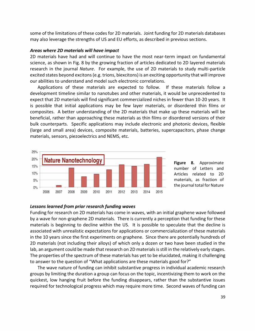
39
some of the limitations of these codes for 2D materials. Joint funding for 2D materials databases may also leverage the strengths of US and EU efforts, as described in previous sections.
Areas where 2D materials will have impact 2D materials have had and will continue to have the most near-term impact on fundamental science, as shown in Fig. 8 by the growing fraction of articles dedicated to 2D layered materials research in the journal Nature. For example, the use of 2D materials to study multi-particle excited states beyond excitons (e.g. trions, biexcitons) is an exciting opportunity that will improve our abilities to understand and model such electronic correlations.
Applications of these materials are expected to follow. If these materials follow a development timeline similar to nanotubes and other materials, it would be unprecedented to expect that 2D materials will find significant commercialized niches in fewer than 10-20 years. It is possible that initial applications may be few layer materials, or disordered thin films or composites. A better understanding of the 2D materials that make up these materials will be beneficial, rather than approaching these materials as thin films or disordered versions of their bulk counterparts. Specific applications may include electronic and photonic devices, flexible (large and small area) devices, composite materials, batteries, supercapacitors, phase change materials, sensors, piezoelectrics and NEMS, etc.
Lessons learned from prior research funding waves Funding for research on 2D materials has come in waves, with an initial graphene wave followed by a wave for non-graphene 2D materials. There is currently a perception that funding for these materials is beginning to decline within the US. It is possible to speculate that the decline is associated with unrealistic expectations for applications or commercialization of these materials in the 10 years since the first experiments on graphene. Since there are potentially hundreds of 2D materials (not including their alloys) of which only a dozen or two have been studied in the lab, an argument could be made that research on 2D materials is still in the relatively early stages. The properties of the spectrum of these materials has yet to be elucidated, making it challenging to answer to the question of “What applications are these materials good for?”
The wave nature of funding can inhibit substantive progress in individual academic research groups by limiting the duration a group can focus on the topic, incentivizing them to work on the quickest, low hanging fruit before the funding disappears, rather than the substantive issues required for technological progress which may require more time. Second waves of funding can
Figure 8. Approximate number of Letters and Articles related to 2D materials, as fraction of the journal total for Nature Nanotechnology.

40
create a challenge for groups who lost funding after the first wave and are now out of phase with the state of the field.
The breakout session participants feel that attempts to limit the rapid decline of funding after the waves can help alleviate these problems. A “reasonable” level of funding must be maintained to avoid being out of phase with substantive progress.
4.3 Synthesis and Scalability Summary
4.3.1. Technical Highlights On Day 2 of the workshop, Session I was extensively focused on bringing to light discussion on synthesis and scalability of 2D layered materials. Synthesis of high quality materials in scalable ways marks the most important challenge in the emergence of any new material. Carbon nanotubes and graphene are excellent examples of materials where roadblocks remain due to materials synthesis issues. While isolating single layers of 2D layered crystals through mechanical exfoliation has proven to be the natural choice for quickly unveiling their intriguing properties and exploring their device possibilities, there is an urgent need to explore novel synthesis techniques that can provide a path for scalable manufacturing. This topic was centered on two techniques for synthesizing 2D layered materials, specifically, a) Solution-based Synthesis, and b) Vapor-based Synthesis, which were discussed at the workshop.
a) Solution-based Synthesis: For the large scale synthesis of 2D layered nanomaterials, solvent based exfoliation methods have been demonstrated recently which yield mono and few layer nanosheets.104 Such materials have proven valuable in forming hybrid and composite materials, potentially in a scalable manner. Recent work on solution-based processing of 2D layered materials has shown the promise of ink-jet printing to print a diverse array of 2D materials over large areas in order to combine their complimentary properties for functional structures.105,106 It is not surprising that such solution-based techniques result in material that contains more structural imperfections compared to other approaches such as vapor-based techniques, but the materials maybe adequate for low-end electronics applications, such as flexible and printed electronics. Scientists presenting their work on the solution-based synthesis of 2D materials at this workshop included: Cinzia Casiraghi, Claudia Backes on behalf of Jonathan Coleman from Trinity College, Yuri Gogotsi and Mark Hersam.
In Cinzia Casiraghi’s talk, she discussed solution based approaches for the realization of heterostructures derived from 2D layered materials. The inks formulated by her group are not composed of organic solvents, which are often toxic, expensive, and have high boiling point, but they have developed water-based inks that are suitable for ink-jet printing, with particular applicability for flexible electronics.107 While Claudia Backes, who represented Jonathan Coleman, was unable to make it to the workshop due to a last minute emergency, Coleman’s group continues to be a pioneer in the liquid phase exfoliation of 2D layered nanomaterials that show promise for large volume production as deciphered from Fig. 9.104,108 Yuri Gogotsi discussed

41
his work on transition metal carbides (Ti2C, Ti3C2, Nb4C3, etc.) and carbonitrides where the selective etching of the A-group element from a MAX phase results in the formation of 2D Mn+1Xn solids, labeled “MXene”. Eleven different carbides and carbonitrides have been reported to date. Some of the potential applications of these materials such as 2D Ti3C2 are in electrical energy storage devices, in particular batteries, Li-ion capacitors and supercapacitors. Mark Hersam discussed his group’s work in utilizing manufacturable approaches at ambient conditions for the integration of 2D materials that range from dielectrics, contacts, and other semiconductors. His talk focused on efforts to improve the uniformity of solution-processed 2D layered materials such as MoS2, WS2, MoSe2, WSe2, boron nitride and black phosphorus, for large-area scalability.
b) Vapor-based Synthesis: Non-solution based approaches such as chemical or physical vapor deposition, as well as atomic layer deposition, offer more control on the physical properties of 2D layered materials which is important for electronics, photonics or magnetic device applications where defect-free materials are highly desirable. Unlike the vapor-based growth techniques for graphene and carbon nanotubes which require catalysts for growth, the synthesis of 2D chalcogenide materials is not a catalytic process. One way for synthesizing MoS2 is to expose deposited Mo metal to a sulphur vapor by heating a solid sulphur source to temperatures in excess of 700ºC.109 Another interesting report that has emerged recently presents a synthetic technique that can enable the growth of centimeter-scale, uniform, high-quality MoS2 films with controlled layer number.110 Such reports hold promise for the production of uniform, large-area sheets of TMDCs and other 2D layered materials. Other reports on the CVD synthesis of 2D layered materials have also emerged recently for the realization of vertical heterostructures of various TMDCs,111 lateral heterostructures WS2/MoS2, and variable-band-gap monolayer alloys WxMo1-xS,112 MoSxSe1-x
113 and BCN.114 Leading scientists who presented their work on this topic at the workshop included talks by Joshua Robinson, Manish Chhowalla, Juerg Osterwalder, and Mauricio Terrones. Joshua Robinson talked about the direct synthesis of 2D materials using techniques as such as metal-organic chemical vapor deposition for the formation of MoS2, WSe2, MoS2/WSe2, and hBN on epitaxial graphene; direct growth leads to superior interfaces and coupling to the substrate when compared to exfoliation. Manish Chhowalla has utilized phase engineering to study the phase transition of 2D materials induced through chemical means. Complex metal TMDCs assume the 1T phase where the transition metal atom coordination is octahedral. The 2H phase is stable in semiconducting TMDCs where the coordination of metal atoms is trigonal prismatic. He has been able to convert 2H phase 2D TMDCs to the 1T phase. The chemically converted 1T phase of MoS2 exhibits interesting properties that are being exploited for catalysis for hydrogen evolution
Figure 9. High-throughput production of solution exfoliated 2D layered materials. Reprinted with permission from Ref. 108 (Fig. 1), Copyright © Macmillan Publishers Ltd: Nature (2014).
42
reaction, source and drain electrodes in high performance FETs, and as electrodes for energy storage. Juerg Osterwalder has utilized surface science approaches to prepare high-quality graphene and h-BN heterostacks with CVD on different single-crystalline metal substrates such as Cu (111)115 and Rh (111). His team has also developed a low-cost photoelectron yield setup for in-situ process monitoring.116 Mauricio Terrones discussed the synthesis of high quality monolayers of nitrogen-, silicon- and boron-doped graphene sheets on Cu foils using ambient-pressure chemical vapor deposition (AP-CVD). He also talked about the synthesis of WS2 and MoS2 triangular monolayers, as well as large area films using a high temperature sulfurization of WOx clusters deposited on insulating substrates.
4.3.2. Report for Break-out Topic 3: “Synthesis and Scalability”
Break-out Session Leaders:
US-Chair: Manish Chhowalla, Rutgers University; EU-Chair: Juerg Osterwalder, University of Zurich; Scribe: Mauricio Terrones, Penn State University.
Participants: Ludwig Bartels, Tony Ivanov, Yury Gogotsi, Michael McConney, Albert Davydov, Joshua Robinson, Joan Redwing, Jeremy Robinson, Andrey Voevodin, Shanee Paciley, Luigi Colombo, Jeff Kelber, Josh Goldberger, Michael Check, Lincoln Lauhon, Robert Wallace
There was a general consensus that rapid progress in 2D materials growth was being made. Recent demonstration of uniform thin films on 4” wafer scale by the Cornell group is a promising step. However, despite the large number of papers on synthesis of 2D materials and their lateral and vertical heterostructures, the general opinion of the breakout group was that uniform and controllable growth over large area remains a key challenge for the field.
Much of the discussion focused on device applications of 2D materials and to this end, it was discussed that the community would benefit from more intimate interactions between the materials growers and device researchers. This is already occurring through several funded projects and additional efforts devoted to these sorts of interactions will be beneficial for the community. Scalability and reproducibility were voiced to be the primary challenges that need to be addressed for the device applications. Doping, control over the number of layers, heteroepitaxy for vertical integration, were also highlighted as unresolved issues that must be addressed. Finally, despite the emergence of phosphorene as an exciting 2D material, it cannot be directly grown currently.
To address these challenges, various deposition methods were discussed. The current widely used chemical vapor deposition methods were thought to be unsuitable for scalable growth of TMDCs. Molecular Beam Epitaxy was argued as a tool for achieving high quality materials but perhaps not sufficiently selective. Metal organic CVD was thought to be a feasible way to achieve large area uniform growth of 2D materials. However, there were discussions about liquid phase approaches to growth, including electrochemical atomic layer deposition, that provide possible opportunities that have not been explored in this recent 2D era. (Luigi pointed out that liquid phase epitaxy is the only way to make high quality II-VI materials.)

43
The goals for growth studies should be: To understand nucleation and growth, and how to achieve heteroepitaxy. To grow oriented films on amorphous substrates (not possible with 3-D materials). Determine the dimensions over which single crystal films are possible. Develop atomic layer deposition methods to demonstrate precise control over number of layers. Develop methodology for controllable doping. In addition to electronics, there are numerous applications where large quantities of 2D materials in the form of nanosheets would be useful. These include energy applications (storage, catalysis etc.), flexible electronics (e.g. inks), and fillers for composites. Tremendous progress has been made in this area in synthesis of 2D materials such as MXenes and transition metal dichalcogenides. To focus the synthesis and growth effort, the community could benefit from development of technology roadmaps that are focused. There is a need to develop several roadmaps to cover a range of applications. Some general comments: Think broadly about applications. Recognize near-term applications. Continue materials exploration to generate solutions for problems not yet identified.
5. Summary and Recommendations
The field of 2D layered materials and devices is accelerating at a rapid pace and significant contributions have been made to the field by researchers in Europe and the United States. This inaugural workshop between the US and EU in the area of 2D layered materials and devices, received tremendous interest from the community and presented a unique opportunity to bring together leading researchers from the two continents to address the opportunities and the challenges for this dynamic field in the coming years. In doing so, it is envisioned that this workshop can serve as a nucleation point to help catalyze synergistic joint cross-Atlantic collaborative activities between researchers to help accelerate research progress and the eventual technological impact of these materials on society.
As discussed at the workshop, the pool of 2D crystals encompasses diverse compositions that lead to a wide spectrum of properties ranging from metallic systems (e.g. graphene, TiS2, TaS2, NiSe2, and NbSe2) to insulating (e.g. hBN); intermediate to these are the semiconducting 2D layered materials (e.g. MoS2, MoSe2, WS2, WSe2, ZrS2, GaSe, InSe). These unique properties can be combined into hybrid architectures from the bottom-up using a lego-type framework to form composites or heterostructures exhibiting pristine, atomic-scale interfaces that conventionally scaled 3D materials fail to provide. Some of the new research directions for this field that have emerged in the last several years include exploring correlated and exictonic effects, such as two-particle bound hole and electron, or three-particle interactions. Another research direction that

44
has emerged recently includes the exploration of exotic elemental 2D semiconducting materials such as phosphorene and silicene which have the potential to provide a paradigm shift in device possibilities.
Despite the fact that these materials possess intriguing properties which fuels our scientific curiosity, an equally important consideration is our ability to mass produce and manufacture these materials in scalable ways to increase the likelihood of translational opportunities arising in the future. The field is ripe with tremendous potential for basic science and discovery, and for potentially spawning disruptive technologies, and it is imperative that an adequate amount of resources be allocated to enable further innovations to bear fruit in the future. Some of the cross-cutting recommendations deduced from the workshop are provided below, to help guide the strategic directions for the field, and the allocation of resources and future investments.
1. Enhancing Manufacturing Research
There was a general consensus at this workshop that despite the large number of papers on the synthesis of 2D materials and their lateral and vertical heterostructures, uniform and controllable growth of 2D materials over large area remains a key challenge for the field. The community would benefit from more intimate interactions between the materials growers and device researchers. This is already occurring through several funded projects and additional efforts devoted to foster more such interactions will be beneficial for the community. Scalability and reproducibility were voiced to be the primary challenges that need to be addressed. Doping, control over the number of layers, heteroepitaxy for vertical integration, were also highlighted as unresolved issues that must be addressed. In recent years, the US federal government has invested significantly in manufacturing research through the creation of the National Network for Manufacturing Innovation (NNMI). These manufacturing centers which are under the umbrella of the NNMI are selected in strategic topical and geographical areas throughout the US, and may pose an opportunity for 2D materials through interagency cooperation and engagement with industry and related partners. A program similar to the NSF scalable nanomanufacturing initiative would also be an equally beneficial avenue to fund smaller teams of investigators, particularly in the case where industry are involved and assist with prototyping as is the case with the NSF GOALI program as well. Agencies such as NIST could have an important role to play in providing material standards. In addition, having focused technology-driven roadmaps besides the one that already exists for the electronics industry through the ITRS road map, would be beneficial to consider for 2D materials for a wider variety of industrial sectors, such as flexible electronics, energy applications (e.g. storage, catalysis), or fillers for composites; some of the example sectors may present a more near-term market for 2D materials where defects and disorder are more tolerable and sometimes even desired for maximal performance. 2. Enhancing Research on Characterization Tools & Techniques
At the workshop through the talks and discussions, there was agreement that it is highly desirable to integrate characterization tools with growth tools. Given the 2D materials are all surface, surface science techniques can be readily employed: Auger spectroscopy, X-ray photoelectron
45
spectroscopy (XPS), Reflection high electron energy diffraction (RHEED), Low electron energy microscopy (LEEM), Photoemission electron microscopy (PEEM), Scanning tunneling microscopy (STM) and other transport methods. The desire to integrate transmission electron microscopy (TEM) with material growth was also discussed, as it would open up the potential for in situ analysis to “slice” 2D crystals with desired thicknesses; femtosecond lasers can also be integrated with the growth for time resolved studies to shed insights into growth mechanisms and surface chemistry. Other tools that may help address the challenge of small lateral size typical of 2D materials synthesis includes near-field or sub-wavelength spectroscopy, multi-probe conduction atomic force microscopy (AFM), and nanoscale angular resolved photoemission spectroscopy (nano-ARPES). Characterization tools and the development of new methods to analyze 2D atomic layers should be supported as they would accelerate the development of high-quality 2D materials.
3. Supporting Heterostructure Research
This workshop showcased tremendous advances that have taken place in the last several years, in the construction of 3D structures using 2D layered materials, which act as building blocks from the bottom-up. The electronic, optical, mechanical and thermal properties of heterostructures and stacks, including dielectric proximity effects and excitonic behavior, can offer new functionalities for applications in electronics, photonics, plasmonics, photo-voltaics, sensing, spin-based magnetic systems and related areas. Supporting research in heterostructures is clearly an area of immense opportunity to harness the unique properties of 2D layered materials.
4. Supporting Modeling and Simulation Research
Through discussions held at this workshop, it was clear that theory and modeling can play an important role in predicting the properties of new atomic layered materials, and to probe structure-property correlations. Concerted efforts in theory and modeling should work hand-in-hand with experimental research to validate and fine-tune the theoretical models. Focused efforts in theory and modeling can prove valuable in understanding the mechanisms for excitons and exotic electronic excited states, as well as dielectric screening effects. Currently theoretical methods are lacking the ability to calculate valley lifetimes which are important for valleytronic devices. The elucidation of properties relevant for spin transport and the identification of materials with strong spin-orbit coupling can facilitate fundamental science and applications arising from these materials for areas such as topological insulators. Understanding the mechanical properties and the role of plasticity in few layer materials also seems of great relevance for flexible devices, but this is a challenging problem requiring multi-scale approaches. The establishment of a materials property database related to 2D materials may be an opportunity for a US-EU collaboration. There are likely to be hundreds of pure 2D materials and many more alloys of these materials. Efforts to identify and characterize all possible defects, edge states, and stable phases may also be incorporated into this database. The format of such a database could be similar to the nanoHUB, and include the ability to distribute codes and code inputs. In particular, in the area of modeling and simulation, much of the materials electronic

46
structure code development is currently being developed by the EU, through mechanisms such as VASP, Quantum Espresso, Abinit, etc. Collaborative activities between US-EU researchers in the area of modeling and simulation may be helpful for sharing and disseminating the modeling tools and knowledge more widely.
5. Funding Interdisciplinary Teams for Center-like Efforts
A significant number of the talks presented at the workshop essentially captured the sense that many important fundamental issues still need to be addressed for 2D materials research which cut across disciplines. Breakthroughs in the field of 2D materials and devices is likely to occur through the collective expertise of researchers from many disciplines including physics, chemistry and engineering, and to form interdisciplinary research teams involving synthesis, chemistry, characterization, theory, and device fabrication. Large center-like efforts, co-sponsored by multiple agencies and industry will help bridge the “valley-of-death” to ensure translation of device prototypes to a manufacturing technology. A closer connection between industry and end-user of the technology is perceived as being beneficial to the community. Industry can set meaningful metrics for benchmarking and a roadmap for the technologies can be developed, where input from industry is critical under the umbrella of a center-like effort.
6. Incentivizing Engagement with Industry
During the workshop discussions, the following were suggested as potential “killer” applications of 2D materials which included: flexible and wearable electronics and photonics, strain sensors, night vision, energy applications such as supercapacitors, composite materials that take advantage of the structural and thermal properties of 2D materials, bio-sensing, bio-compatible devices and other bio-related applications. Strong engagement with industry is of paramount importance to translate the promise of these materials for practical applications. Approaches to incentivize engagement with industry should be considered. Examples in the past include the Semiconductor Research Corporation’s efforts to promote graphene research through the creation of the Nanoelectronic Research Initiative (NRI) or the South West Academy of Nanoelectronics (SWAN) center.
7. Enhancing Collaboration between US and EU Researchers & Administrators
This workshop generated tremendous interest amongst the participants from the EU and the US, with the hope that it will help catalyze partnerships and collaborations in strategic areas between leading researchers and administrators from the two regions. The community agrees that it is beneficial to collaborate taking advantage of the expertise and infrastructure available in the two regions. Several of the US agencies are open to proposals from Europe and there are some mechanisms at both the US and EU to help finance travel. At the workshop, it was discussed that mechanisms which fund one-to-one US-EU collaborations are clearly lacking. Some of the mechanisms for encouraging more collaborative activities which were discussed at the workshop

47
included: (1) Joint conference support to cover cost of travel to enable participants to attend these workshops/conferences; (2) Joint US/EU 2D seminar series, which could be webcast with minimal cost; (3) Personnel exchange programs that involve the bi-lateral exchange of faculty, graduate students and post-doctoral fellows; (4) Fellowships awarded to students for joint US/EU collaborative activities. A metric for measuring the progress of such collaborations could be gauged through the number and quality of the joint publications that emerge from such collaborations. The NSF International Programs Office may have an avenue to fund supplemental grants to currently funded PIs to promote such educational outreach and student exchange programs. Besides advancing the fundamental research of 2D layered materials through such exchange programs, these activities will also facilitate in the training of a globally engaged workforce which should help promote science and engineering breakthroughs in the present-day global economy. For these programmatic activities to emerge, it would be beneficial for the NSF to work jointly with counterpart EU Agencies to help promote such cross-Atlantic collaborations.
8. Ensuring a Sustained Level of Funding
The workshop participants felt that a “reasonable” level of sustained funding must be maintained for long-term progress, irrespective of geography. There was perception that the wave nature of funding can inhibit substantive progress in individual academic research groups by limiting the duration a group can focus on the topic, incentivizing them to work on the quickest, low hanging fruit before the funding disappears, rather than the substantive issues required for technological progress which may require more time. Stability of funding in basic science, as well as development of novel applications in 2D materials is needed. The participants felt that the field of 2D layered materials is still relatively “young” with numerous material compositions that have yet to be explored. Therefore expectations for these materials should be more realistic in terms of commercialization prospects which can take many years.
Conclusion
In conclusion, the talks and the break-out discussions at the workshop were in synergy with the workshop goals. We would once again like to thank all of the invited speakers, panelists and guests for their participation and contributions at this workshop, and for making it a successful event to help propel this exciting field forward through the recommendations put-forth through this workshop.
48
References
1 K. S. Novoselov, A. K. Geim, S. V. Morozov, D. Jiang, Y. Zhang, S. V. Dubonos, I. V. Grigorieva, and A. A. Firsov, Science 306, 666 (2004).
2 K. Novoselov, et al., “A roadmap for graphene,” Nature 490, 192 (2012). 3 Y. –M. Lin, C. Dimitrakopoulos, K. A. Jenkins, D. B. Farmer, H-Y Chiu, A. Grill, and P. Avouris, “100-
GHz transistors from wafer-scale epitaxial graphene,” Science 327, 662 (2010). 4 T. K. Agarwal, A. Nourbakhsh, P. Raghavan, I. Radu, S. De Gendt, M. Heyns, M. Verhelst, and A. Thean,
“Bilayer graphene tunneling FET for sub-0.2 V digital CMOS logic applications” IEEE Electron Device Letters 35, 1308 (2014).
5 S. Park, S. Lee, G. Mordi, S. Jandhyala, M. W. Ha, J. S. Lee, L. Colombo, R. M. Wallace, B. H. Lee, and J. Kim, “Triangular-pulse measurement for hysteresis of high-performance and flexible graphene field-effect transistors” IEEE Electron Device Letters 35, 277 (2014).
6 Y.-M. Lin, A. Valdes-Garcia, S.-J. Han, D. B. Farmer, I. Meric, Y. Sun, Y. Wu, C. Dimitrakopoulos, A. Grill, P. Avouris and K. A. Jenkins, “Wafer-scale graphene integrated circuit,” Science 332, 1294 (2011).
7 N. Savage, “One graphene device makes three amplifiers,” IEEE Spectrum 47, 15 (2010). 8 J. S. Moon, H. C. Seo, M. Antcliffe, D. Le, C. McGuire, et al. “Graphene FETs for zero-bias linear resistive
FET mixers,” IEEE Electron Device Letters 34, 465 (2013). 9 W. S. Zhao, D. W. Wang, G. Wang, et al., “Electrical modeling of on-chip Cu-graphene heterogeneous
interconnects” IEEE Electron Device Letters 36, 74 (2015). 10 X. Y. Chen, D. H. Seo, S. Seo, H. Chung, and H. S. P. Wong “Graphene interconnect lifetime: A reliability
analysis,” IEEE Electron Device Letters 33, 1604 (2012). 11 M. C. Chen, C. L Hsu, and T. J. Hsueh, “Fabrication of humidity sensor based on bilayer graphene” IEEE
Electron Device Letters 35, 590 (2014). 12 B. Chakrabarti, T. Roy, and E. M. Vogel, “Nonlinear switching with ultralow reset power in graphen-
insulator-graphene forming-free resistive memories” IEEE Electron Device Letters 35, 750 (2014). 13 W. Cao, J. H. Kang, S. Bertolazzi, A. Kis, and K. Banerjee “Can 2D-nanocrystals extend the lifetime of
floating-gate transistor based nonvolatile memory,” IEEE Transactions on Electron Devices 61, 3456 (2014).
14 R. Courtland, “Graphene goes the distance in spintronics,” IEEE Spectrum 50, 15 (2013). 15 S. Bae, H. Kim, Y. Lee, X. Xu, J. S. Park, Y. Zheng, J. Balakrishnan, T. Lei, H. Ri Kim, Y. I. Song, Y. J. Kim,
K. S. Kim, B. Özyilmaz, J. H. Ahn, B. H. Hong and S. Iijima, “Roll-to-roll production of 30-inch graphene films for transparent electrodes,” Nature Nanotechnol. 5, 574 (2010).
16 C. Yan, J. H. Cho and J.-H. Ahn, “Graphene-based flexible and stretchable thin film transistors,” Nanoscale 4, 4870 (2012).
17 J. Lee, T. J. Ha, K. N. Parrish, S. F. Chowdhury, L. Tao, A. Dodabalapur, and D. Akinwande “High-performance current saturating graphene field-effect transistor with hexagonal boron nitride dielectric on flexible polymeric substrates,” IEEE Electron Device Letters 34, 172 (2013).
18 P. Genevet and F. Capasso, “Breakthrough in Photonics 2013: Flat optics: wavefronts control with Huygens” IEEE Photonics Journal 6, 0700404 (2014).
19 Z. W. Pei, H. C. Lai, Y. J. Wang, W. H. Chiang and C. H. Chen, “High-responsivity and high-sensitivity graphene dots/a-IGZO thin film phototransistor” IEEE Electron Device Letters 36, 44 (2015).
20 L. Jiang, X. Dai, Y. Xiang, “Tunable group delay of the optical pulse reflection from Fabry-Perot cavity with the insertion of graphene sheets,” IEEE Photonics Journal 6, 3200109 (2014).

49
21 Y. M. Gao, D.H. Song, S. S. Chu, Z. G. Chen, “Artificial graphene and related photonic lattices generated
with a simple method,” IEEE Photonics Journal 6, 2201806 (2014). 22 S. Haigh, et al. “Cross-sectional imaging of individual layers and buried interfaces of graphene-based
heterostructures and superlattices,” Nature Mater. 11, 764 (2012). 23 L. Ponomarenko, et al., “Cloning of Dirac fermions in graphene superlattices,” Nature 497, 594 (2013). 24 B. Hunt, et al., “Massive Dirac Fermions and Hofstadter Butterfly in a van der Waals Heterostructure,”
Science 340, 1427 (2013). 25 G. Yu, et al., “Hierarchy of Hofstadter states and replica quantum Hall ferromagnetism in graphene
superlattices,” Nature Physics 10, 525 (2014). 26 Q. H. Wang, K. Kalantar-Zadeh, A. Kis, J. N. Coleman, and M. S. Strano, “Electronics and optoelectronics
of two-dimensional transition metal dichalcogenides,” Nature Nano. 7, 699 (2012). 27 A. Geim and I. Grigorieva, “Van der Waals heterostructures,” Nature 499, 419 (2013). 28 K. Novoselov, et al., “Two-dimensional atomic crystals,” PNAS 102, 10451 (2005). 29 M. Xu, et al., “Graphene-like two-dimensional materials,” Chem. Rev. 113, 3766 (2013). 30 A. B. Kaul, “Two-dimensional layered materials: structure, properties and prospects for device
applications,” J. Mater. Res. 29, 348 (2014). 31 M. Osada and T. Sasaki, “Two-Dimensional Dielectric Nanosheets: Novel Nanoelectronics From
Nanocrystal Building Blocks,” Adv. Mater. 24, 210 (2012). 32 N. Savage, “Graphene’s new rival,” IEEE Spectrum 49, 15 (2012). 33 K. Alam and R. K. Lake “Monolayer MoS2 transistors beyond the technology road map” IEEE
Transactions on Electron Devices 59, 3250 (2012). 34 K. F. Mak, C. Lee, J. Hone, J. Shan, and T. F. Heinz, “Atomically think MoS2: A new direct-gap
semiconductor,” Phys. Rev. Lett. 105, 136805 (2010). 35 A. Splendiani, L. Sun, Y. B. Zhang, T. S. Li, J. Kim, C. Y. Chim, et al, “Emerging photoluminescence in
monolayer MoS2,” Nano Lett. 10, 1271 (2010). 36 Y. D. Ma, Y. Dai, M. Guo, C. W. Niu, J. B. Lu, B. B. Huang, “ Electronic and magnetic properties of
perfect, vacancy-doped, and nonmetal adsorbed MoSe2, MoTe2 and WS2 monolayers,” Phys. Chem. Chem. Phys. 13, 15546 (2011).
37 H. J. Conley, B. Wang, J. I. Ziegler, R. F. Haglund, S. T. Pantelides, and K. I. Bolotin: Bandgap engineering of strained monolayer and bilayer MoS2. Nano Lett. 13, 3626 (2013).
38 K. He, C. Poole, K. F. Mak, and J. Shan, “Experimental demonstration of continuous electronic structure tuning via strain in atomically thin MoS2,” Nano Lett. 13, 2931 (2013).
39 P. Lu, X. Wu, W. Guo, and X. C. Zeng, “Strain-dependent electronic and magnetic properties of MoS2 monolayer, bilayer, nanoribbons and nanotubes,” Phys. Chem. Chem. Phys. 14, 13035 (2012).
40 E. Scalise, M. Houssa, G. Pourtois, V. Afanasev, A. Stesmans, “Strain-induced semiconductor to metal transition in the two dimensional honeycomb structure of MoS2,” Nano Res. 5, 43 (2012).
41 L. Britnell, et al, “Field-effect tunneling transistor based on vertical graphene heterostructures,” Science 335, 947 (2012).
42 T. Georgiou, et al. “Vertical field-effect transistor based on graphene–WS2 heterostructures for flexible and transparent electronics,” Nature Nanotechnol. 8, 100 (2013).
43 L. Britnell, R. M. Ribeiro, A. Eckmann, R. Jalil, B. D. Belle, A. Mishchenko, Y.-J. Kim, R. V. Gorbachev, T. Georgiou, S. V. Morozov, A. N. Grigorenko, A. K. Geim, C. Casiraghi, A. H. Castro Neto, and K. S. Novoselov, “Strong light-matter interactions in heterostructures of atomically thin films,” Science 340, 1311 (2013).
44 L. Britnell, et al., “Resonant tunnelling and negative differential conductance in graphene transistors,” Nature Comm. 4, 1794 (2013).

50
45 A. Mishchenko, et al. “Twist-controlled resonant tunnelling in graphene/boron nitride/graphene
heterostructures,” Nature Nanotechnol. 9, 808 (2014). 46 F. Withers, O. Del Pozo-Zamudio, A. Mishchenko, A. P. Rooney, A. Gholinia, K. Watanabe,T. Taniguchi,
S. J. Haigh, A. K. Geim, A. I. Tartakovskii , and K. S. Novoselov, “Light-emitting diodes by band-structure engineering in van der Waals heterostructures,” Nature Materials 14, 301-306 (2015).
47 W. J. Zhao, Z. Ghorannevis, L. Q. Chu, M. L. Toh, C. Kloc, P. H. Tan, and G. Eda, “Evolution of electronic structure in atomically thin sheets of WS2 and WSe2,” ACS Nano 7, 791 (2013).
48 A. Ramasubramaniam, D. Naveh, and E. Towe, “Tunable band gaps in bilayer transition-metal dichalcogenides,” Phys. Rev. B 84, 205325 (2011).
49 Z. Yin, H. Li, H. Li, L. Jiang, Y. Shi, Y. Sun, G. Lu, G. Lu, Q. Zhang, X. Chen, and H. Zhang, “Single-layer MoS2 phototransistors,” ACS Nano 6, 74 (2012).
50 H. S. Lee, S. W. Min, Y. G. Chang, M. K Park, T. Nam, H. Kim, et al., “MoS2 nanosheet phototransistors with thickness-modulated optical energy gap,” Nano Lett. 12, 3695 (2012).
51 A. Polman and H. A. Atwater, “Photonic design principles for ultrahigh-efficiency photovoltaics,” Nature Mater. 11, 174 (2012).
52 M. Bernardi, M. Palummo, and J. C. Grossman, “Extraordinary sunlight absorption and 1 nm-thick photovoltaics using two-dimensional monolayer materials,” Nano Lett. 13, 3664 (2013).
53 B. Ganchev, N. Drummond, I. Aleiner, and V. Fal’ko, “Three-particle complexe in two-dimensional semiconductors,” Phys. Rev. Lett. 114, 107401 (2015).
54 A. Srivastava, M. Sidler, A. V. Allain, D. S. Lembke, A. Kis, and A. Imamoğlu, “Valley Zeeman effect in elementary optical excitations of monolayer Wse2,” Nature Phys. 11, 141 (2015).
55 A. Srivastava, M. Sidler, A. V. Allain, D. S. Lembke, A. Kis, and A. Imamoğlu, “Optically active quantum dots in monolayer WSe2,” Nature Nanotech. 10, 491 (2015).
56 A. Ferrari et al., “Science and technology roadmap for graphene related two-dimensional crystals, and hybrid systems,” Nanoscale 7, 4587 (2015).
57 S. Schwarz, S. Dufferwiel, P. M. Walker, F. Withers, et al.,”Two-dimensional metal-chalcogenide films in tunable optical microcavities,” Nano Lett. 14, 7003 (2014).
58 L. Prechtel, L. Song, D. Schuh, P. Ajayan, W. Wegscheider, and A.W. Holleitner “Time-resolved ultrafast photocurrents and terahertz generation in freely suspended graphene,” Nature Comm. 3, 646 (2012).
59 A. Brenneis, L. Gaudreau, M. Seifert, H. Karl, M.S. Brandt, H. Huebl, J.A. Garrido, F.H.L. Koppens, and A.W. Holleitner “Ultrafast electronic readout of diamond nitrogen-vacancy centres coupled to graphene,” Nature Nanotech. 10, 135 (2015).
60 C. Kastl, C. Karnetzky, H. Karl, and A.W. Holleitner “Ultrafast helicity control of surface currents in topo-logical insulators with near-unity fidelity,” Nature Comm. 6, 6617 (2015).
61 W. J. Yu, Y. Liu, H. Zhou, A. Yin, Z. Li, Y. Huang, and X. Duan, “Highly efficient gate-tunable photocurrent generation in vertical heterostructures of layered materials,” Nature Nano. 8, 952 (2013).
62 R. K. Ghosh and S. Mahapatra “Direct band-to-band tunneling in reverse biased MoS2 nanoribbon p-n junctions,” IEEE Transactions on Electron Devices 60, 274 (2013).
63 A. Seabaugh “The tunneling transistor,” IEEE Spectrum 50, 35 (2013). 64 B. Radisavljevic, et al., “Single-layer MoS2 transistors,” Nature Nanotechnol. 6, 147 (2011). 65 B. Radisavljevic, M. B. Whitwick, and A. Kis, “Integrated circuits and logic operations based on single-
layer MoS2,” ACS Nano 5, 9934 (2011). 66 Y. C. Du, H. Liu, A. T. Neal, M. W. Si, and P. D. Ye “Molecular doping of multilayer MoS2 field-effect
transistors: reduction in sheet and contact resistances,” IEEE Electron Device Letters 34, 1328 (2013). 67 J. S. Moon, H. C. Seo, F. Stratan, M. Antcliffe, A. Schmitz, et al. “Lateral graphene heterostructure field-
effect transistor,” IEEE Electron Device Letters 34, 1190 (2013).

51
68 M. P. Levendorf, C. J. Kim, L. Brown, P. Y. Huang, R. W. Havener, D. A. Muller, J. Park, “Graphene and
boron nitride lateral heterostructrures for atomically thin circuitry,” Nature 488, 627 (2012). 69 H. Liu and P. D. D. Ye, “MoS2 dual-gate MOSFET with atomic-layer deposition Al2O3 as top-gate
dielectric,” IEEE Electron Device Letters 33, 546 (2012). 70 Q. Zhang, G. Iannaccone, and G. Fiori “Two-dimensional tunnel transistors based on Bi2Se3 thin film,”
IEEE Electron Device Letters 35, 129 (2014). 71 G. Fiori, F. Bonaccorsco, G. Iannaccone, T. Palacios, D. Neumaier, A. Seabaugh, S. K. Banerjee, and L.
Colombo “Electronics based on two-dimensional materials,” Nature Nanotech. 9, 768 (2014). 72 L. T. Liu, Y. Lu, and J. Guo “On monolayer MoS2 field-effect transistors at the scaling limit,” IEEE
Transactions on Electron Devices 60, 4133 (2013). 73 K. Majumdar, C. Hobbs, and P. D. Kirsch “Benchmarking transition metal dichalcogenides MOSFET in
the ultimate physical scaling limit,” IEEE Electron Device Letters 35, 402 (2014). 74 Q. Zhang, Y. Q. Lu, C. A. Richter, D. Jena, and A. Seabaugh, “Optimum bandgap and supply voltage in
tunnel FETs,” IEEE Transactions on Electron Devices 61, 2719 (2014). 75 H. Wang, L. L Yu, Y. H. Lee, Y. M. Shi, A. Hsu, M. L. Chin, L. J. Li, M. Dubey, J. Kong, T. Palacios,
“Integrated circuits based on bilayer MoS2 transistors,” Nano Lett. 12, 4674 (2012). 76 C. Yim, M. O’Brien, N. McEvoy, S. Riazimehr, H. Schäfer-Eberwein, A. Bablich, R. Pawar, G. Iannaccone,
C. Downing, G. Fiori, M. C. Lemme, and G. S. Duesberg, “Heterojunction hybrid devices from vapor phase grown MoS2,” Sci. Rep. 4, 5458 (2014).
77 G. Lupina, J. Kitzmann, I. Costina, M. Lukosius, C. Wenger, A. Wolff, S. Vaziri, M. Östling, I. Pasternak, A. Krajewska, W. Strupinski, S. Kataria, A. Gahoi, M. C. Lemme, G. Ruhl, G. Zoth, O. Luxenhofer, and W. Mehr, “Residual metallic contamination of transferred chemical vapor deposited graphene,” ACS Nano 9, 4776 (2015).
78 Y. Y. Illarionov, A. D. Smith, S. Vaziri, M. Ostling, T. Mueller, M. C. Lemme, T. Grasser, “Bias-temperature instability in single-layer graphene field-effect transistors,” Appl. Phys. Lett. 105, 143507 (2014).
79 A. Hellemans, “The quest for 2-D silicon,” IEEE Spectrum 49, 16 (2012). 80 F. Liu, Y. J. Wang, X. Y. Liu, J. Wang, and H. Guo “Ballistic transport in monolayer black phosphorus
transistors,” IEEE Transactions on Electron Devices 61, 3871 (2014). 81 X. Cao and J. Guo “Simulation of phosphorene field-effect transistor at the scaling limit,” IEEE
Transactions on Electron Devices 62, 659 (2015). 82 K. T. Lam, Z. P. Dong, and J. Guo, “Performance limits projection of black phosphorous field-effect
transistors,” IEEE Electron Device Letters 35, 963 (2014). 83 P. Vogt, P. De Padova, C. Quaresima, J. Avila, et al. “Silicene : compelling experimental evidence for
graphene-like two-dimensional silicon,” Phys. Rev. Lett. 108 (2012) 155501 84 P. De Padova, C. Ottaviani, C. Quaresima, et al. “24 h stability of thick multilayer silicene in air,”2D
Materials 1 (2014) 021003. 85 L. Tao, E. Cinquanta, D. Chiappe, C. Grazianetti, M. Fanciulli, M. Dubey, A. Molle, and D.
Akinwande, “Silicene field-effect transistors operating at room temperature,”Nature Nanotechnol. 10, 227 (2015).
86 G. Le Lay, “2D Materials : Silicene transistorse,”Nature Nanotechnol. 10, 202 (2015). 87 M. E. Dávila, L. Xian, S. Cahangirov, A. Rubio, G. Le Lay, “Germanene: a novel two-dimensional
germanium allotrope akin to graphene and silicene,” New J. Phys. 16 (2014) 095002. 88 H. Liu, A. T. Neal, Z. Zhu, Z. Luo, X. Xu, D. Tomanek and P. D. Ye, “Phosphorene: An unexplored 2D
semiconductor with a high hole mobility,” ACS Nano 8, 4033 (2014). 89 C. Ataca, H. Sahin, and S. J. Ciraci: Stable, single-layer MX2 transition-metal oxides and dichalcogenides
in a honeycomb-like structure. Phys. Chem. C 116(16), 8983 (2012).

52
90 J. Feng, X. Qian, C. Huang, and J. Li, “Strain-engineered artificial atom as a broad-spectrum solar energy
funnel,” Nature Photonics 6, 2 (2012). 91 V.I. Artyukhov, Y. Hao, R.S. Ruoff, and B.I. Yakobson, “Breaking of symmetry in graphene growth on
metal substrates,”Phys. Rev. Lett. 114, 115502 (2015). 92 X. Zhang, L. Wang, J. Xin, B. I. Yakobson, F. Ding, “Role of hydrogen in graphene chemical vapor
deposition growth on a copper surface,” J. Amer. Chem. Soc. 136, 3040 (2014). 93 Y. Liu, Y.M. Wang, B. I. Yakobson, B.C. Wood, “Assessing carbon-based anodes for lithium-ion
batteries: A universal description of charge-transfer binding,” Phys. Rev. Lett. 113, 028304 (2014). 94 A.G. Kvashnin, L.A. Chernozatonskii, B. I. Yakobson, P.B. Sorokin, “Phase diagram of quasi-two-
dimensional carbon, from graphene to diamond,” Nano Lett. 14, 676 (2014). 95 A. Aziz, et al. “Dislocation motion and grain boundary migration in two dimensional WS2,” Nature
Comm. 5, 4867 (2014). 96 Y. Liu, F. Xu, Z. Zhang, E.S. Penev, B. I. Yakobson, “Two-dimensional mono-elemental semiconductor
with electronically inactive defects: The case of phosphorus,” Nano Lett. 14, 6782 (2014). 97 L. Wang, A. Kutana, X. Zou, and B.I. Yakobson, “Electro-mechanical anisotropy of phosphorene,”
Nanoscale, in press (2015). 98 A. Kormányos, G. Burkard, M. Gmitra, J. Fabian. V. Zólyomi, N. D. Drummond, and V. I. Fal'ko, “k.p
theory for two-dimensional transition metal dichalcogenide semiconductors,” 2D Materials 2, 020011 (2015).
99 A. Kormányos, V. Zólyomi, N. D. Drummond, P. Rakyta, G. Burkard, and V. I. Fal'ko, “Monolayer MoS2: trigonal warping, “Γ-valley” and spin-orbit coupling effects,” Phys. Rev. B 88, 045416 (2013).
100 A. Kormányos, V. Zólyomi, N. D. Drummond, and G. Burkard, “Spin-orbit coupling, quantum dots, and qubits in monolayer transition metal dichalcogenides,” Phys. Rev. X 4, 011034 (2014).
101 Karel-Alexander N. Duerloo, Mitchell T. Ong, and Evan J. Reed, “Intrinsic piezoelectricity in two-dimensional materials,” J. Phy. Chem. Lett. 3, 2871 (2012).
102 Karel-Alexander N. Duerloo and Evan J. Reed, “Flexural electromechanical coupling: A nanoscale emergent property of boron nitride bilayers,” Nano Lett. 13, 1681 (2013).
103 K.-A. Duerloo, Y. Li, and E. J. Reed, “ Structural phase transitions in two-dimensional Mo- and W-dichalcogenide monolayers,” Nature Comm. 5, 4214 (2014).
104 J. Coleman, et al., “Two-Dimensional Nanosheets Produced by Liquid Exfoliation of Layered Materials,” Science 331, 568 (2011).
105 J. Li, M. M. Naiini, S. Vaziri, M. C. Lemme, and M. Ostling, “Inkjet printing MoS2,” Adv. Func. Matl. 24, 6525 (2014).
106 F. Withers, H. Yang, L. Britnell, A. P. Rooney, E. Lewis, A. Felten, C. R. Woods, V. Sanchez Romaguera, et al. “Heterostructures produced from nanosheet-based inks,” Nano Lett. 14, 3987 (2014).
107 H. Yang, F. Withers, E. Gebremedhn, E. Lewis, L. Britnell, A. Felten, V. Palermo, S. Haigh, D. Beljonne, and C. Casiraghi, “Dielectric nanosheets made by liquid-phase exfoliation in water and their use in graphene-based electronics,” 2D Materials 1, 011012 (2014).
108 K. R. Paton, “Scalable production of large quantities of defect-free few-layer graphene by shear exfoliation in liquids,” Nature Materials 13, 624 (2014).
109 Y. Zhan, Z. Liu, S. Najmaei, P. M. Ajayan, and J. Lou, “Large-area vapor phase growth and characterization of MoS2 atomic layers on a SiO2 substrate,” Small 8, 966 (2012).
110 Y. Yu, C. Li, Y. Liu, L. Su, Y. Zhang, and L. Cao, “Controlled scalable synthesis of uniform, high-quality monolayer and few layer MoS2 films,” Scientific Reports 3, 1866 (2013).
111 Y. Gong, J. Lin, X. Wang, G. Shi, et al. “Vertical and in-plane heterostructures from WS2/MoS2 monolayers,” Nature Materials 13, 1135-1142 (2014).

53
112 Z. Liu et al, “Composition-dependent Raman modes of Mo1-xWxS2 monolayer alloys,” Nanoscale 6,
2833 (2014). 113 Y. Gong, et al. “Band Gap Engineering and Layer-by-Layer Mapping of Selenium-Doped Molybdenum
Disulfide,” Nano Lett. 14, 442 (2014). 114 Y. Gong et al, “Direct Chemical Conversion of Graphene to Boron- and Nitrogen- and Carbon-
containing Atomic Layers,” Nature Comm. 5, 3193 (2014). 115 S. Roth, F. Matsui, T. Gerber, and J. Osterwalder, “Chemical vapor deposition and characterization of
aligned and incommensurate graphene/hexagonal boron nitride heterostack on Cu(111),” Nano Lett. 13, 2668 (2013).
116 A. Hemmi, H. Cun, S. Roth, J. Osterwalder, and T. Greber, “Low cost photoelectron yield setup for surface process monitoring,” J. Vac. Sci. Technol. A 32, 02302 (2014).