Non-adiabatic ab initio molecular dynamics of supersonic ...ucfbdxa/pubblicazioni/jcp13.pdf ·...
9
Non-adiabatic ab initio molecular dynamics of supersonic beam epitaxy of silicon carbide at room temperature Simone Taioli, Giovanni Garberoglio, Stefano Simonucci, Silvio a Beccara, Lucrezia Aversa et al. Citation: J. Chem. Phys. 138, 044701 (2013); doi: 10.1063/1.4774376 View online: http://dx.doi.org/10.1063/1.4774376 View Table of Contents: http://jcp.aip.org/resource/1/JCPSA6/v138/i4 Published by the American Institute of Physics. Additional information on J. Chem. Phys. Journal Homepage: http://jcp.aip.org/ Journal Information: http://jcp.aip.org/about/about_the_journal Top downloads: http://jcp.aip.org/features/most_downloaded Information for Authors: http://jcp.aip.org/authors
Transcript of Non-adiabatic ab initio molecular dynamics of supersonic ...ucfbdxa/pubblicazioni/jcp13.pdf ·...
Non-adiabatic ab initio molecular dynamics of supersonic beam epitaxy ofsilicon carbide at room temperatureSimone Taioli, Giovanni Garberoglio, Stefano Simonucci, Silvio a Beccara, Lucrezia Aversa et al. Citation: J. Chem. Phys. 138, 044701 (2013); doi: 10.1063/1.4774376 View online: http://dx.doi.org/10.1063/1.4774376 View Table of Contents: http://jcp.aip.org/resource/1/JCPSA6/v138/i4 Published by the American Institute of Physics. Additional information on J. Chem. Phys.Journal Homepage: http://jcp.aip.org/ Journal Information: http://jcp.aip.org/about/about_the_journal Top downloads: http://jcp.aip.org/features/most_downloaded Information for Authors: http://jcp.aip.org/authors
THE JOURNAL OF CHEMICAL PHYSICS 138, 044701 (2013)
Non-adiabatic ab initio molecular dynamics of supersonic beam epitaxyof silicon carbide at room temperature
Simone Taioli,1,2,3,4,a) Giovanni Garberoglio,1 Stefano Simonucci,1,3,5 Silvio a Beccara,1,2
Lucrezia Aversa,6 Marco Nardi,6,7 Roberto Verucchi,8 Salvatore Iannotta,9
Maurizio Dapor,1,10,11 and Dario Alfè12,13,14,15
1Interdisciplinary Laboratory for Computational Science, FBK-Center for Materials and Microsystems andUniversity of Trento, Trento, Italy2Department of Physics, University of Trento, Trento, Italy3Istituto Nazionale di Fisica Nucleare, Sezione di Perugia, Italy4Department of Chemistry, University of Bologna, Bologna, Italy5Department of Physics, University of Camerino, Camerino, Italy6Institute of Materials for Electronics and Magnetism, IMEM-CNR, Trento, Italy7Institut für Physik, Humboldt-Universität zu Berlin, Berlin, Germany8Institute of Materials for Electronics and Magnetism, FBK-CNR, Trento, Italy9Institute of Materials for Electronics and Magnetism, IMEM-CNR, Parma, Italy10Department of Materials Engineering and Industrial Technologies, University of Trento, Trento, Italy11Istituto Nazionale di Fisica Nucleare, Sezione di Padova, Italy12Department of Earth Sciences, University College London, London, United Kingdom13Department of Physics and Astronomy, University College London, London, United Kingdom14London Centre for Nanotechnology, University College London, London, United Kingdom15Thomas Young Centre @ UCL, University College London, London, United Kingdom
(Received 17 October 2012; accepted 14 December 2012; published online 22 January 2013)
In this work, we investigate the processes leading to the room-temperature growth of silicon car-bide thin films by supersonic molecular beam epitaxy technique. We present experimental datashowing that the collision of fullerene on a silicon surface induces strong chemical-physical per-turbations and, for sufficient velocity, disruption of molecular bonds, and cage breaking withformation of nanostructures with different stoichiometric character. We show that in these out-of-equilibrium conditions, it is necessary to go beyond the standard implementations of density func-tional theory, as ab initio methods based on the Born-Oppenheimer approximation fail to capture theexcited-state dynamics. In particular, we analyse the Si-C60 collision within the non-adiabatic nu-clear dynamics framework, where stochastic hops occur between adiabatic surfaces calculated withtime-dependent density functional theory. This theoretical description of the C60 impact on the Sisurface is in good agreement with our experimental findings. © 2013 American Institute of Physics.[http://dx.doi.org/10.1063/1.4774376]
I. INTRODUCTION
A fundamental problem in materials science is theunderstanding and control of epitaxy mechanisms for theproduction of high-quality crystals. In particular, thin filmcrystal growth of silicon carbide (SiC), a semiconductor syn-thesized to replace silicon in harsh working conditions, inopto- and micro-electronics, and in biomedical and biosens-ing applications,1 is affected by many factors, notably thetemperature. In the usual thin film growth processes, a depo-sition temperature in excess of 1000 K is used to synthesizethis material and speed up growth and nucleation. However, ahigher growth temperature results in a larger number of crys-tallographic defects, such as voids, stacking faults, and dislo-cations. The presence of these defects represents a substantialdrawback as it strongly influences the electronic and opticalproperties of SiC in a uncontrollable way. Furthermore, thetemperature issue is emphasized in SiC growth, as one has to
a)Author to whom correspondence should be addressed. Electronic mail:[email protected].
deal with the different thermal expansion (8% larger in SiC)of lattice-mismatched substrates (20% larger in Si) inducingstress and strain in the grains. Therefore, a reduction of thegrowth temperature of SiC thin films represents an undisputedadvantage.
To achieve this reduction down to room temperature con-ditions, we present in this work a technique2 based on super-sonic molecular beams of fullerene (C60) impinging on a Sisurface (SuMBE). By seeding a carrier gas, such as H2, He,and Ar, within an injection chamber with the material to de-posit (in our case carbon), and by using aerodynamical accel-eration to reach supersonic velocities out of the injection cell,high fluence, and directionality of the particles towards theSi surface can be obtained with a substantial freezing of theinternal degrees of freedom to typical temperatures of a fewkelvins.2 In this way, different processes, such as cage disrup-tion, Si-C covalent bond formation, and, finally, SiC growthcan be activated.
After presenting experimental evidence of SiC formationat room temperature by electron spectroscopy of core (XPS)and valence bands (UPS)3 for a 35 eV C60 beam impinging
0021-9606/2013/138(4)/044701/8/$30.00 © 2013 American Institute of Physics138, 044701-1
044701-2 Taioli et al. J. Chem. Phys. 138, 044701 (2013)
on a Si(111) reconstructed (7×7) surface, our analysis willbe mainly focused on the theoretical modeling of the C60
cage rupture, which triggers all further chemical-physical pro-cesses. Furthermore, this investigation will enable us to en-visage the role of the C60 kinetic energy in initiating the SiCgrowth and driving the chemical reactions.
The study of high-energy cluster beam impact on solidsurfaces is an old topic,4 both from a theoretical and exper-imental point of view, with many applications ranging frommaterials science, for sputtering5 or thin film deposition,6
to chemistry, for initiating reactions,7, 8 and even nuclear fu-sion experiments.9 In particular, the studies of C60 impacton semiconductor surfaces are important in materials sciencefor the growth of carbon-based nanostructures. Several rea-sons make C60 a very good precursor for SiC epitaxy. First,C60 is the most abundant among fullerenes, and can be inex-pensively obtained either by a discharge between two nearbygraphite electrodes in an inert atmosphere, or by other self-assembly mechanisms that have been recently proposed.10
Second, this molecule has a large total mass and thus canbe accelerated in the SuMBE experiment by exploiting theaerodynamical acceleration mechanism.11, 12 Finally, hydro-gen is not present in pristine fullerene, avoiding the pres-ence of an undesired chemical element into a SiC growingfilm.
On the other hand, state-of-the-art experimental and the-oretical investigations in high-energy cluster beam impactsare far from being conclusive on the nature of the chemi-cal and physical processes occurring at the surface. WhileSiC epitaxy has been already achieved in experiments,11, 12
the right stoichiometric ratio was obtained only above 800 Kand for a beam kinetic energy of 5 eV. However, availablecomputer simulations based on classical molecular dynamics(MD)13 or tight-binding approach14 are in complete disagree-ment with these experiments. In these studies Si structuralorder is maintained, with simple superficial permeation andno evidence of C60 cage breaking up to an energy per atomthree times the experimental value obtained by SuMBE. Inthis paper, we show that the reason of the failure in explain-ing the C60 cage rupture at the observed kinetic energy is theneglect of the coupling between the electronic and nuclear de-grees of freedom within the widely used Born-Oppenheimer(BO) approximation. To overcome this limitation, we de-cided to describe the coupled electronic-nuclear dynamics viaa non-adiabatic approach.15 In fact, recent modeling effortspoint out the importance of non-adiabatic effects in describ-ing various physical and chemical phenomena occurring atsurfaces.16–18
This paper is structured in the following way. InSec. II, we briefly outline the experimental apparatus andtechniques used to obtain the SiC growth. Experimental ev-idence of the SiC growth at room temperature by electronspectroscopy is provided in Sec. III. The ensuing calcu-lation of the fullerene cage impact on the Si(111)-(7×7)surface by different methods within BO approximation isthen described in Sec. IV. Section V illustrates the re-sults obtained by switching-on non-adiabatic surface hoppingmethod to describe the C60 rupture for the problem of SiCepitaxy.
II. EXPERIMENTAL TECHNIQUES
The study has been performed at the IMEM-CNR lab-oratory where an experimental setup, devoted to ultrahighvacuum (UHV) thin film growth by SuMBE and in situanalysis, has been developed. A detailed description of thistechnique is provided by Ref. 2. The supersonic beam isformed in a separate “source chamber” (base pressure of1 × 10−7 mbar) while film deposition and characterizationis performed in the main μ-metal chamber at a pressure of3 × 10−11 mbar. Auger (AES), X-ray (XPS), and ultravio-let (UPS) photoemission electron spectroscopies can be per-formed. XPS spectra have been taken using Mg Kα photons at1253.6 eV, while the valence band structure was probed usingthe HeI 21.2 eV of a Helium discharge lamp. The electron en-ergy analyzer, a VG hemispherical device (CLAM2), allowsa total energy resolution of 0.95 eV for XPS and about 0.1 eVfor UPS. The C60 source is essentially made of two coaxialquartz capillary tubes, resistively heated by a tantalum foil.The experiments were carried out using free-jet expansionsof H2 in which the seeded fullerene particles, using appropri-ate low percentages, reach a kinetic energy of about 35 eV,with an average growth rate of about 0.1 Å/min in the direc-tion perpendicular to the substrate. The substrates used wereobtained from a Si(111) wafer (resistivity 1.20 × 10⁻⁴ �m)cleaned by a modified Shiraki procedure.12 The silicon ox-ide film was then removed in vacuum by several annealingcycles, until a Si(111)-(7×7) surface reconstruction was ob-tained, as checked by the well-known sharp LEED pattern.The core level analysis has been performed by Voigt lineshapedeconvolution after background subtraction by a Shirley func-tion. The typical precision for peak energy positioning is±0.05 eV, uncertainty for full width at half maximum(FWHM) is less than 5% and for area evaluation is about2.5%.
III. EXPERIMENTAL FINDINGS
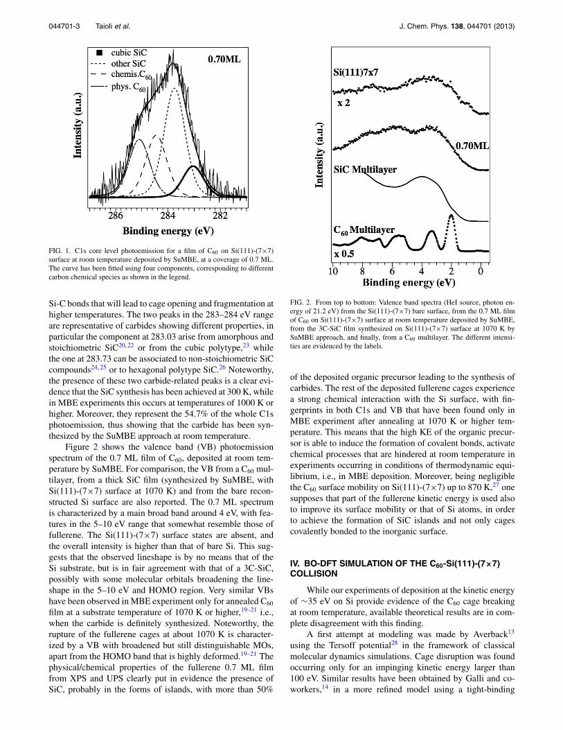
C60 supersonic molecular beams by SuMBE techniquehave been used to grow high quality crystalline SiC thin films.In this method, the formation and cleavage of bonds and theactivation of surface processes are kinetically driven. Epitaxyexperiments at room temperature have been carried out aim-ing to estimate the effects of the initial kinetic energy onthe growth without thermal contributions. Fig. 1 shows theC1s core level of a 0.7 monolayer (ML) fullerene film de-posited at room temperature by SuMBE. The peak lineshapeis quite complex and four components have been introducedto achieve the best curve fit, showing the same FWHM of1.00 eV. The features are located at binding energies (BE)of 283.03, 283.73, 284.46, and 285.10 eV and are character-ized by a percentage over the whole C1s signal of 12.0%,42.7%, 23.4%, and 21.9%, respectively. The peak at higherBE is typical of physisorbed C60 at room temperature depo-sition, possibly showing covalent interaction between a fewfullerene carbon atoms and the silicon surface.19–21 The struc-ture at 284.46 eV has been observed only in MBE experi-ments where the substrate temperature was at least 700 K; it isconsidered representative of the formation of several covalent
044701-3 Taioli et al. J. Chem. Phys. 138, 044701 (2013)
FIG. 1. C1s core level photoemission for a film of C60 on Si(111)-(7×7)surface at room temperature deposited by SuMBE, at a coverage of 0.7 ML.The curve has been fitted using four components, corresponding to differentcarbon chemical species as shown in the legend.
Si-C bonds that will lead to cage opening and fragmentation athigher temperatures. The two peaks in the 283–284 eV rangeare representative of carbides showing different properties, inparticular the component at 283.03 arise from amorphous andstoichiometric SiC20, 22 or from the cubic polytype,23 whilethe one at 283.73 can be associated to non-stoichiometric SiCcompounds24, 25 or to hexagonal polytype SiC.26 Noteworthy,the presence of these two carbide-related peaks is a clear evi-dence that the SiC synthesis has been achieved at 300 K, whilein MBE experiments this occurs at temperatures of 1000 K orhigher. Moreover, they represent the 54.7% of the whole C1sphotoemission, thus showing that the carbide has been syn-thesized by the SuMBE approach at room temperature.
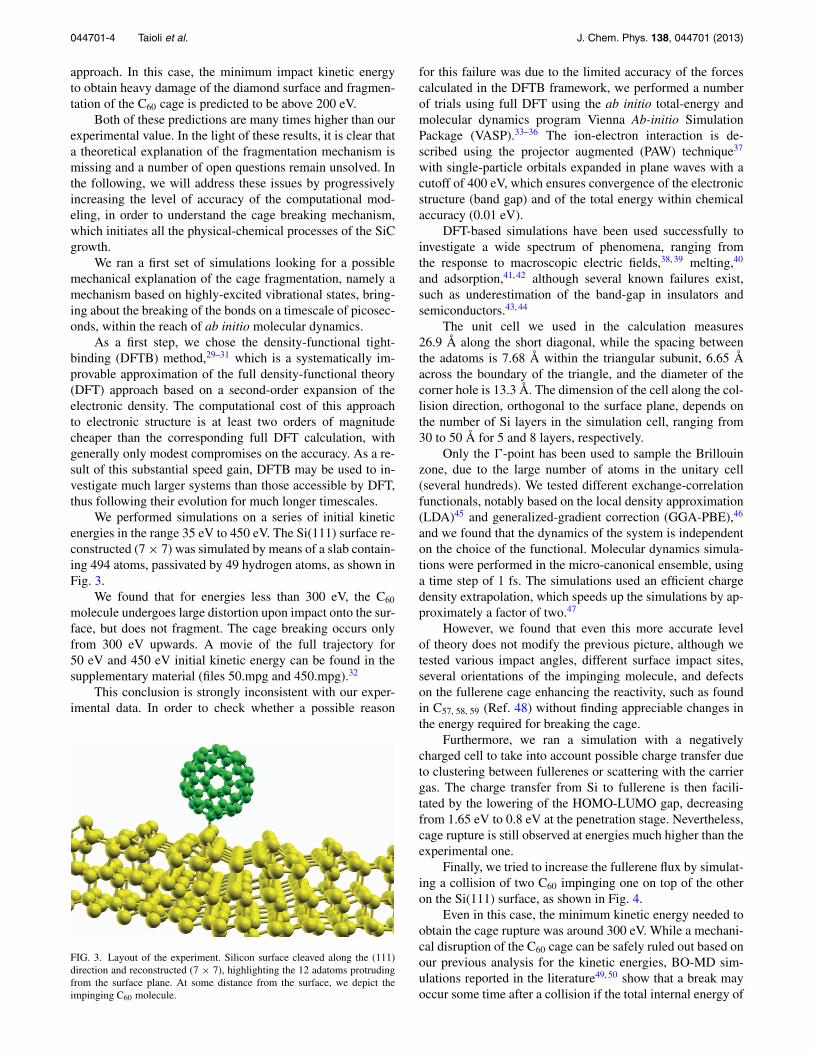
Figure 2 shows the valence band (VB) photoemissionspectrum of the 0.7 ML film of C60, deposited at room tem-perature by SuMBE. For comparison, the VB from a C60 mul-tilayer, from a thick SiC film (synthesized by SuMBE, withSi(111)-(7×7) surface at 1070 K) and from the bare recon-structed Si surface are also reported. The 0.7 ML spectrumis characterized by a main broad band around 4 eV, with fea-tures in the 5–10 eV range that somewhat resemble those offullerene. The Si(111)-(7×7) surface states are absent, andthe overall intensity is higher than that of bare Si. This sug-gests that the observed lineshape is by no means that of theSi substrate, but is in fair agreement with that of a 3C-SiC,possibly with some molecular orbitals broadening the line-shape in the 5–10 eV and HOMO region. Very similar VBshave been observed in MBE experiment only for annealed C60
film at a substrate temperature of 1070 K or higher,19–21 i.e.,when the carbide is definitely synthesized. Noteworthy, therupture of the fullerene cages at about 1070 K is character-ized by a VB with broadened but still distinguishable MOs,apart from the HOMO band that is highly deformed.19–21 Thephysical/chemical properties of the fullerene 0.7 ML filmfrom XPS and UPS clearly put in evidence the presence ofSiC, probably in the forms of islands, with more than 50%
FIG. 2. From top to bottom: Valence band spectra (HeI source, photon en-ergy of 21.2 eV) from the Si(111)-(7×7) bare surface, from the 0.7 ML filmof C60 on Si(111)-(7×7) surface at room temperature deposited by SuMBE,from the 3C-SiC film synthesized on Si(111)-(7×7) surface at 1070 K bySuMBE approach, and finally, from a C60 multilayer. The different intensi-ties are evidenced by the labels.
of the deposited organic precursor leading to the synthesis ofcarbides. The rest of the deposited fullerene cages experiencea strong chemical interaction with the Si surface, with fin-gerprints in both C1s and VB that have been found only inMBE experiment after annealing at 1070 K or higher tem-perature. This means that the high KE of the organic precur-sor is able to induce the formation of covalent bonds, activatechemical processes that are hindered at room temperature inexperiments occurring in conditions of thermodynamic equi-librium, i.e., in MBE deposition. Moreover, being negligiblethe C60 surface mobility on Si(111)-(7×7) up to 870 K,27 onesupposes that part of the fullerene kinetic energy is used alsoto improve its surface mobility or that of Si atoms, in orderto achieve the formation of SiC islands and not only cagescovalently bonded to the inorganic surface.
IV. BO-DFT SIMULATION OF THE C60-Si(111)-(7×7)COLLISION
While our experiments of deposition at the kinetic energyof ∼35 eV on Si provide evidence of the C60 cage breakingat room temperature, available theoretical results are in com-plete disagreement with this finding.
A first attempt at modeling was made by Averback13
using the Tersoff potential28 in the framework of classicalmolecular dynamics simulations. Cage disruption was foundoccurring only for an impinging kinetic energy larger than100 eV. Similar results have been obtained by Galli and co-workers,14 in a more refined model using a tight-binding
044701-4 Taioli et al. J. Chem. Phys. 138, 044701 (2013)
approach. In this case, the minimum impact kinetic energyto obtain heavy damage of the diamond surface and fragmen-tation of the C60 cage is predicted to be above 200 eV.
Both of these predictions are many times higher than ourexperimental value. In the light of these results, it is clear thata theoretical explanation of the fragmentation mechanism ismissing and a number of open questions remain unsolved. Inthe following, we will address these issues by progressivelyincreasing the level of accuracy of the computational mod-eling, in order to understand the cage breaking mechanism,which initiates all the physical-chemical processes of the SiCgrowth.
We ran a first set of simulations looking for a possiblemechanical explanation of the cage fragmentation, namely amechanism based on highly-excited vibrational states, bring-ing about the breaking of the bonds on a timescale of picosec-onds, within the reach of ab initio molecular dynamics.
As a first step, we chose the density-functional tight-binding (DFTB) method,29–31 which is a systematically im-provable approximation of the full density-functional theory(DFT) approach based on a second-order expansion of theelectronic density. The computational cost of this approachto electronic structure is at least two orders of magnitudecheaper than the corresponding full DFT calculation, withgenerally only modest compromises on the accuracy. As a re-sult of this substantial speed gain, DFTB may be used to in-vestigate much larger systems than those accessible by DFT,thus following their evolution for much longer timescales.
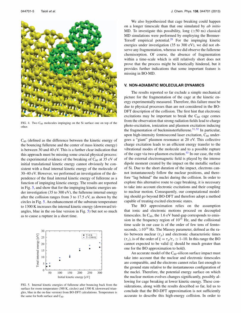
We performed simulations on a series of initial kineticenergies in the range 35 eV to 450 eV. The Si(111) surface re-constructed (7 × 7) was simulated by means of a slab contain-ing 494 atoms, passivated by 49 hydrogen atoms, as shown inFig. 3.
We found that for energies less than 300 eV, the C60
molecule undergoes large distortion upon impact onto the sur-face, but does not fragment. The cage breaking occurs onlyfrom 300 eV upwards. A movie of the full trajectory for50 eV and 450 eV initial kinetic energy can be found in thesupplementary material (files 50.mpg and 450.mpg).32
This conclusion is strongly inconsistent with our exper-imental data. In order to check whether a possible reason
FIG. 3. Layout of the experiment. Silicon surface cleaved along the (111)direction and reconstructed (7 × 7), highlighting the 12 adatoms protrudingfrom the surface plane. At some distance from the surface, we depict theimpinging C60 molecule.
for this failure was due to the limited accuracy of the forcescalculated in the DFTB framework, we performed a numberof trials using full DFT using the ab initio total-energy andmolecular dynamics program Vienna Ab-initio SimulationPackage (VASP).33–36 The ion-electron interaction is de-scribed using the projector augmented (PAW) technique37
with single-particle orbitals expanded in plane waves with acutoff of 400 eV, which ensures convergence of the electronicstructure (band gap) and of the total energy within chemicalaccuracy (0.01 eV).
DFT-based simulations have been used successfully toinvestigate a wide spectrum of phenomena, ranging fromthe response to macroscopic electric fields,38, 39 melting,40
and adsorption,41, 42 although several known failures exist,such as underestimation of the band-gap in insulators andsemiconductors.43, 44
The unit cell we used in the calculation measures26.9 Å along the short diagonal, while the spacing betweenthe adatoms is 7.68 Å within the triangular subunit, 6.65 Åacross the boundary of the triangle, and the diameter of thecorner hole is 13.3 Å. The dimension of the cell along the col-lision direction, orthogonal to the surface plane, depends onthe number of Si layers in the simulation cell, ranging from30 to 50 Å for 5 and 8 layers, respectively.
Only the �-point has been used to sample the Brillouinzone, due to the large number of atoms in the unitary cell(several hundreds). We tested different exchange-correlationfunctionals, notably based on the local density approximation(LDA)45 and generalized-gradient correction (GGA-PBE),46
and we found that the dynamics of the system is independenton the choice of the functional. Molecular dynamics simula-tions were performed in the micro-canonical ensemble, usinga time step of 1 fs. The simulations used an efficient chargedensity extrapolation, which speeds up the simulations by ap-proximately a factor of two.47
However, we found that even this more accurate levelof theory does not modify the previous picture, although wetested various impact angles, different surface impact sites,several orientations of the impinging molecule, and defectson the fullerene cage enhancing the reactivity, such as foundin C57, 58, 59 (Ref. 48) without finding appreciable changes inthe energy required for breaking the cage.
Furthermore, we ran a simulation with a negativelycharged cell to take into account possible charge transfer dueto clustering between fullerenes or scattering with the carriergas. The charge transfer from Si to fullerene is then facili-tated by the lowering of the HOMO-LUMO gap, decreasingfrom 1.65 eV to 0.8 eV at the penetration stage. Nevertheless,cage rupture is still observed at energies much higher than theexperimental one.
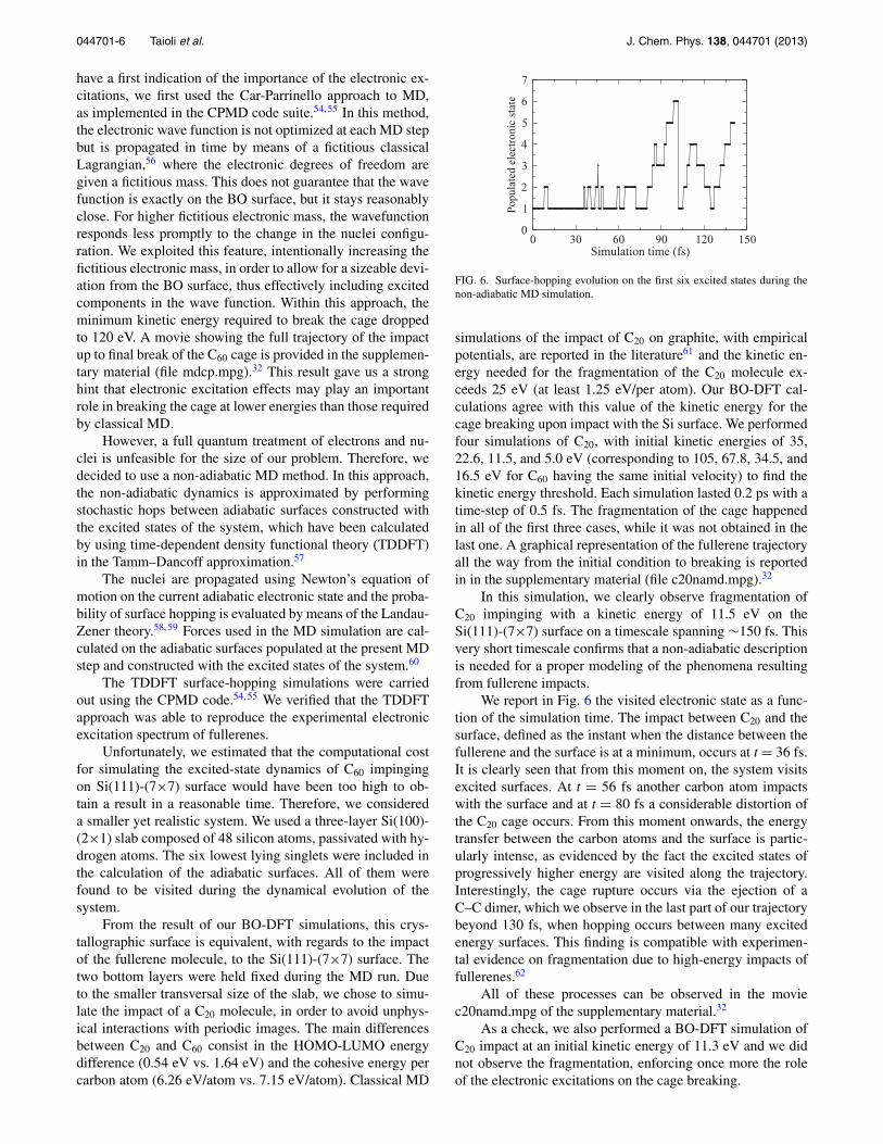
Finally, we tried to increase the fullerene flux by simulat-ing a collision of two C60 impinging one on top of the otheron the Si(111) surface, as shown in Fig. 4.
Even in this case, the minimum kinetic energy needed toobtain the cage rupture was around 300 eV. While a mechani-cal disruption of the C60 cage can be safely ruled out based onour previous analysis for the kinetic energies, BO-MD sim-ulations reported in the literature49, 50 show that a break mayoccur some time after a collision if the total internal energy of
044701-5 Taioli et al. J. Chem. Phys. 138, 044701 (2013)
FIG. 4. Two C60 molecules impinging on the Si surface one on top of theother.
C60 (defined as the difference between the kinetic energy ofthe bouncing fullerene and the center of mass kinetic energy)is between 30 and 40 eV. This is a further clear indication thatthis approach must be missing some crucial physical process:the experimental evidence of the breaking of C60 at 35 eV ofinitial translational kinetic energy cannot obviously be con-sistent with a final internal kinetic energy of the molecule of30–40 eV. However, we performed an investigation of the de-pendence of the final internal kinetic energy of fullerene as afunction of impinging kinetic energy. The results are reportedin Fig. 5, and show that for the impinging kinetic energies un-der investigation (35 to 300 eV), the fullerene internal energyafter the collision ranges from 3 to 17.5 eV, as shown by thecircles in Fig. 5. An enhancement of the substrate temperatureto 1300 K increases the internal kinetic energy (downward tri-angles, blue in the on-line version in Fig. 5) but not so muchas to cause a rupture in a short time.
50 100 150 200 250 300Initial kinetic energy [eV]
0
5
10
15
20
25
30
Tot
al in
tern
al e
nerg
y [e
V] T=0 K
T=1300 K
FIG. 5. Internal kinetic energies of fullerene after bouncing back from thesurface for room temperature (300 K, circles) and 1300 K (downward trian-gles, blue in the on-line version) from BO-DFT calculations. Temperature isthe same for both surface and C60.
We also hypothesized that cage breaking could happenon a longer timescale than that one simulated by ab initioMD. To investigate this possibility, long (�50 ns) classicalMD simulations were performed by employing the Brenner-Tersoff empirical potential.28 For the impinging kineticenergies under investigation (35 to 300 eV), we did not ob-serve any fragmentation, whereas we did observe the fullerenechemisorption. Of course, the absence of fragmentationwithin a time-scale which is still relatively short does notprove that the process might be kinetically hindered, but itprovides further indications that some important feature ismissing in BO-MD.
V. NON-ADIABATIC MOLECULAR DYNAMICS
The results reported so far exclude a simple mechanicalpicture for the fragmentation of the cage at the kinetic en-ergy experimentally measured. Therefore, this failure must bedue to physical processes than are not considered in the BO-DFT description of the collision. The first hint that electronicexcitations may be important to break the C60 cage comesfrom the observation that strong radiation fields lead to chargephoto-excitation, ionization and plasmon excitation inducingthe fragmentation of buckminsterfullerene.51, 52 In particular,upon high-intensity femtosecond laser excitation, C60 under-goes a “giant” plasmon resonance at 20 eV. This collectivecharge excitation leads to an efficient energy transfer to thevibrational modes of the molecule and to a possible ruptureof the cage via two-plasmon excitation.53 In our case, the roleof the external electromagnetic field is played by the intensedipole moment created by the impact on the metallic surfaceof Si. Due to the short duration of the impact, electrons can-not instantaneously follow the nuclear positions, and there-fore “lag behind” the nuclei during the collision. In order toexplore this alternative route to cage breaking, it is necessaryto take into account electronic excitations and their couplingto nuclear motion. Consequently, our computational model-ing should go beyond BO-DFT and therefore adopt a methodcapable of treating excited electronic states.
The BO approximation relies on the assumptionthat ionic and electronic motions proceed on decoupledtimescales. In C60, the 1.6 eV band-gap corresponds to emis-sion in the frequency region of 1015 Hz, and the collisionaltime scale in our case is of the order of few tens of femto-seconds, �1014 Hz. The Massey parameter, defined as the ra-tio between nuclear (τ p) and electronic characteristic times(τ e), is of the order of ξ = τ p/τ e � 1–10. In this range the BOcannot expected to be valid (ξ should be much greater thanone for the BO approximation to hold).
An accurate model of the C60-silicon surface impact musttake into account that the nuclear and electronic timescalesare comparable, and the electrons cannot relax fast enough tothe ground state relative to the instantaneous configuration ofthe nuclei. Therefore, the potential energy surface on whichthe nuclear motion evolves changes significantly, possibly al-lowing for cage breaking at lower kinetic energy. These con-siderations, along with the results described so far, led us toconclude that the BO-DFT approximation is not sufficientlyaccurate to describe this high-energy collision. In order to
044701-6 Taioli et al. J. Chem. Phys. 138, 044701 (2013)
have a first indication of the importance of the electronic ex-citations, we first used the Car-Parrinello approach to MD,as implemented in the CPMD code suite.54, 55 In this method,the electronic wave function is not optimized at each MD stepbut is propagated in time by means of a fictitious classicalLagrangian,56 where the electronic degrees of freedom aregiven a fictitious mass. This does not guarantee that the wavefunction is exactly on the BO surface, but it stays reasonablyclose. For higher fictitious electronic mass, the wavefunctionresponds less promptly to the change in the nuclei configu-ration. We exploited this feature, intentionally increasing thefictitious electronic mass, in order to allow for a sizeable devi-ation from the BO surface, thus effectively including excitedcomponents in the wave function. Within this approach, theminimum kinetic energy required to break the cage droppedto 120 eV. A movie showing the full trajectory of the impactup to final break of the C60 cage is provided in the supplemen-tary material (file mdcp.mpg).32 This result gave us a stronghint that electronic excitation effects may play an importantrole in breaking the cage at lower energies than those requiredby classical MD.
However, a full quantum treatment of electrons and nu-clei is unfeasible for the size of our problem. Therefore, wedecided to use a non-adiabatic MD method. In this approach,the non-adiabatic dynamics is approximated by performingstochastic hops between adiabatic surfaces constructed withthe excited states of the system, which have been calculatedby using time-dependent density functional theory (TDDFT)in the Tamm–Dancoff approximation.57
The nuclei are propagated using Newton’s equation ofmotion on the current adiabatic electronic state and the proba-bility of surface hopping is evaluated by means of the Landau-Zener theory.58, 59 Forces used in the MD simulation are cal-culated on the adiabatic surfaces populated at the present MDstep and constructed with the excited states of the system.60
The TDDFT surface-hopping simulations were carriedout using the CPMD code.54, 55 We verified that the TDDFTapproach was able to reproduce the experimental electronicexcitation spectrum of fullerenes.
Unfortunately, we estimated that the computational costfor simulating the excited-state dynamics of C60 impingingon Si(111)-(7×7) surface would have been too high to ob-tain a result in a reasonable time. Therefore, we considereda smaller yet realistic system. We used a three-layer Si(100)-(2×1) slab composed of 48 silicon atoms, passivated with hy-drogen atoms. The six lowest lying singlets were included inthe calculation of the adiabatic surfaces. All of them werefound to be visited during the dynamical evolution of thesystem.
From the result of our BO-DFT simulations, this crys-tallographic surface is equivalent, with regards to the impactof the fullerene molecule, to the Si(111)-(7×7) surface. Thetwo bottom layers were held fixed during the MD run. Dueto the smaller transversal size of the slab, we chose to simu-late the impact of a C20 molecule, in order to avoid unphys-ical interactions with periodic images. The main differencesbetween C20 and C60 consist in the HOMO-LUMO energydifference (0.54 eV vs. 1.64 eV) and the cohesive energy percarbon atom (6.26 eV/atom vs. 7.15 eV/atom). Classical MD
0 30 60 90 120 150Simulation time (fs)
0
1
2
3
4
5
6
7
Pop
ulat
ed e
lect
roni
c st
ate
FIG. 6. Surface-hopping evolution on the first six excited states during thenon-adiabatic MD simulation.
simulations of the impact of C20 on graphite, with empiricalpotentials, are reported in the literature61 and the kinetic en-ergy needed for the fragmentation of the C20 molecule ex-ceeds 25 eV (at least 1.25 eV/per atom). Our BO-DFT cal-culations agree with this value of the kinetic energy for thecage breaking upon impact with the Si surface. We performedfour simulations of C20, with initial kinetic energies of 35,22.6, 11.5, and 5.0 eV (corresponding to 105, 67.8, 34.5, and16.5 eV for C60 having the same initial velocity) to find thekinetic energy threshold. Each simulation lasted 0.2 ps with atime-step of 0.5 fs. The fragmentation of the cage happenedin all of the first three cases, while it was not obtained in thelast one. A graphical representation of the fullerene trajectoryall the way from the initial condition to breaking is reportedin in the supplementary material (file c20namd.mpg).32
In this simulation, we clearly observe fragmentation ofC20 impinging with a kinetic energy of 11.5 eV on theSi(111)-(7×7) surface on a timescale spanning ∼150 fs. Thisvery short timescale confirms that a non-adiabatic descriptionis needed for a proper modeling of the phenomena resultingfrom fullerene impacts.
We report in Fig. 6 the visited electronic state as a func-tion of the simulation time. The impact between C20 and thesurface, defined as the instant when the distance between thefullerene and the surface is at a minimum, occurs at t = 36 fs.It is clearly seen that from this moment on, the system visitsexcited surfaces. At t = 56 fs another carbon atom impactswith the surface and at t = 80 fs a considerable distortion ofthe C20 cage occurs. From this moment onwards, the energytransfer between the carbon atoms and the surface is partic-ularly intense, as evidenced by the fact the excited states ofprogressively higher energy are visited along the trajectory.Interestingly, the cage rupture occurs via the ejection of aC–C dimer, which we observe in the last part of our trajectorybeyond 130 fs, when hopping occurs between many excitedenergy surfaces. This finding is compatible with experimen-tal evidence on fragmentation due to high-energy impacts offullerenes.62
All of these processes can be observed in the moviec20namd.mpg of the supplementary material.32
As a check, we also performed a BO-DFT simulation ofC20 impact at an initial kinetic energy of 11.3 eV and we didnot observe the fragmentation, enforcing once more the roleof the electronic excitations on the cage breaking.
044701-7 Taioli et al. J. Chem. Phys. 138, 044701 (2013)
Following the epitaxy of SiC thin films is computation-ally not feasible due to the time-scale out of reach of MDsimulations, but in principle could be tackled by methodssuch as dominant reaction pathways.63 However, based onthe much higher solubility of carbon at the surface with re-spect to the bulk and the stability of SiC, it could be arguedthat the system, after the cage breaking, will evolve into thestate corresponding to the crystal phase without steep energybarriers.
VI. CONCLUSIONS
In this paper, experiments on the epitaxy of SiC bySuMBE technique and a first-principle model of the colli-sion of C60 with Si(111)-(7×7) surface have been described.SuMBE has been used to grow high quality crystalline SiCthin films. In this experimental method, the formation and dis-ruption of bonds and the activation of surface processes are ki-netically driven. Experiments of deposition at high kinetic en-ergy (∼30–35 eV) on Si gave evidence of SiC ordered domainformation at room temperature. In situ electron spectroscopymeasurements confirm the epitaxy of SiC nano-islands.
Simulations using DFT based on the Born-Oppenheimerand Car-Parrinello approximations are not able to capture thedynamics of the impact, predicting a minimum kinetic en-ergy for the cage breaking of one order of magnitude higherthan the experimental value. This failure is due to the ne-glect in BO-DFT of the excited electronic states, populatedupon the high-energy collision with the Si surface. In orderto properly capture the dynamics of the system, it is manda-tory to explicitly include the excited electronic states in thecalculation.
Therefore, non-adiabatic MD has been used with the in-clusion of several electronic excited states, so as to repro-duce the coupling between the electron and nuclear dynamicsthrough the surface hopping in the calculation of the forces.From our results, we may infer that the mechanism whichmakes it possible to break the fullerene cage at energies aslow as 0.6 eV per atom is the change in the force field felt bythe nuclei, due to the spawning of excited electronic states ofthe molecule upon impact with the surface.
While our theoretical approach and the calculations havebeen performed specifically in the case of SiC growth, we be-lieve that the underlying model and computational tools arerather general, and can be applied to other cases of materialepitaxy or organic molecule interaction by SuMBE with inor-ganic surfaces.
Finally, we would like to comment on the computationalcost of performing these ab initio simulations. All of the BO-DFT calculations presented above required roughly 105 cen-tral processing unit (CPU) hours on modern 2.3 GHz proces-sors of a high-end computing terascale resource. All of thenon-adiabatic simulations required twice as much. The con-siderable computational requirements of non-adiabatic sim-ulations allowed us to follow only the initial stage of theprocesses leading to SiC formation. Nevertheless, this modelagrees with the experimental finding of an energy thresholdfor C60 fragmentation close to 35 eV.
ACKNOWLEDGMENTS
We acknowledge useful discussions with Professor F.Pederiva (University of Trento), A. Bartók-Pártay, and G.Csányi (University of Cambridge). S.T. acknowledges finan-cial support from Provincia Autonoma di Trento, under theMarie-Curie Action “People Programme” of the 7th FP “TheTrentino programme of research, training and mobility ofpost-doctoral researchers—Outgoing Researcher” (2Superbproject). This work made use of the facilities of Aurora,KORE (Bruno Kessler Foundation, Trento) and HECToR, theUnited Kingdom’s national high-performance computing ser-vice, which is provided by UoE HPCx Ltd at the University ofEdinburgh, Cray, Inc., and NAG Ltd, and funded by the Officeof Science and Technology through EPSRC’s High End Com-puting Programme. Finally, S.T. gratefully acknowledges theInstitute of Advanced Studies in Bologna for the logistic sup-port provided during his fellowship.
1EMIS Datareview Series, Vol. 13, edited by G. L. Harris (INSPEC Publi-cation, London, 1995).
2P. Milani and S. Iannotta, Cluster Beam Synthesis of Nano-Structured Ma-terials (Springer-Verlag, Berlin, 1999).
3S. Taioli, S. Simonucci, L. Calliari, and M. Dapor, Phys. Rep. 493, 237(2010).
4G. N. Makarov, Phys. Usp. 49, 117 (2006).5A. Wucher and N. Winograd, Anal. Bioanal. Chem. 396, 105 (2010).6G. Fuchs, M. Treilleux, F. S. Aires, B. Cabaud, P. Melinon, and A. Hoareau,Phys. Rev. A 40, 6128 (1989).
7F. Rohmund, E. E. B. Campbell, O. Knospe, G. Seifert, and R. Schmidt,Phys. Rev. Lett. 76, 3289 (1996).
8T. Raz and R. Levine, Chem. Phys. Lett. 226, 47 (1994).9R. J. Beuhler, G. Friedlander, and L. Friedman, Phys. Rev. Lett. 63, 1292(1989).
10J. Jakowski, S. Irle, and K. Morokuma, Phys. Rev. B 82, 125443(2010).
11L. Aversa, R. Verucchi, G. Ciullo, P. Moras, M. Pedio, L. Ferrari, A. Pesci,and S. Iannotta, Appl. Surf. Sci. 184, 350 (2001).
12R. Verucchi, L. Aversa, G. Ciullo, A. Podestà, P. Milani, and S. Iannotta,Eur. Phys. J. B 26, 509 (2002).
13X. Hu, K. Albe, and R. Averback, J. Appl. Phys. 88, 49 (2000).14G. Galli and F. Mauri, Phys. Rev. Lett. 73, 3471 (1994).15J. C. Tully, J. Chem. Phys. 137, 22A301 (2012).16J. Behler, K. Reuter, and M. Scheffler, Phys. Rev. B 77, 115421 (2008).17D. Matsiev, Z. Li, R. Cooper, I. Rahinov, C. Bartels, D. J. Auerbach, and
A. M. Wodtke, Phys. Chem. Chem. Phys. 13, 8153 (2011).18I. Rahinov, R. Cooper, D. Matsiev, C. Bartels, D. J. Auerbach, and A. M.
Wodtke, Phys. Chem. Chem. Phys. 13, 12680 (2011).19M. D. Seta, N. Tomozeiu, D. Sanvitto, and F. Evangelisti, Surf. Sci. 460,
203 (2000).20K. Sakamoto, D. Kondo, Y. Ushimi, M. Harada, A. Kimura, A. Kakizaki,
and S. Suto, Phys. Rev. B 60, 2579 (1999).21C. Cepek, P. Schiavuta, M. Sancrotti, and M. Pedio, Phys. Rev. B 60, 2068
(1999).22M. Zilani, H. Xu, Y. Sun, X.-S. Wang, and A. Wee, Appl. Surf. Sci. 253,
4554 (2007).23Q. Cheng and S. Xu, J. Appl. Phys. 102, 056101 (2007).24R.-C. Fang and L. Ley, Phys. Rev. B 40, 3818 (1989).25C.-C. Liu, C. Lee, K.-L. Cheng, H.-C. Cheng, and T.-R. Yew, Appl. Phys.
Lett. 66, 168 (1995).26A. Santoni, J. Lancok, V. Dhanak, S. Loreti, G. Miller, and C. Minarini,
Appl. Phys. A 81, 991 (2005).27D. Chen and D. Sarid, Phys. Rev. B 49, 7612 (1994).28J. Tersoff, Phys. Rev. B 37, 6991 (1988).29W. M. Foulkes and R. Haydock, Phys. Rev. B 39, 12520 (1989).30T. Frauenheim, G. Seifert, M. Elstner, T. Niehaus, C. Köhler, M. Amkreutz,
M. Sternberg, Z. Hajnal, A. Di Carlo, and S. Suhai, J. Phys.: Condens.Matter 14, 3015 (2002).
31M. Elstner, D. Porezag, G. Jungnickel, J. Elsner, M. Haugk, T. Frauenheim,S. Suhai, and G. Seifert, Phys. Rev. B 58, 7260 (1998).
044701-8 Taioli et al. J. Chem. Phys. 138, 044701 (2013)
32See supplementary material at http://dx.doi.org/10.1063/1.4774376 formovies of fullerenes impinging on the silicon surfaces.
33G. Kresse and J. Hafner, Phys. Rev. B 47, 558 (1993).34G. Kresse and J. Hafner, Phys. Rev. B 49, 14251 (1994).35G. Kresse and J. Furthmüller, Comput. Mater. Sci. 6, 15 (1996).36G. Kresse and D. Joubert, Phys. Rev. B 59, 1758 (1999).37P. E. Blochl, Phys. Rev. B 50, 17953 (1994).38S. Baroni, S. de Gironcoli, A. D. Corso, and P. Giannozzi, Rev. Mod. Phys.
73, 515 (2001).39B. Chiavarino, M. E. Crestoni, S. Fornarini, S. Taioli, I. Mancini, and P.
Tosi, J. Chem. Phys. 137, 024307 (2012).40S. Taioli, C. Cazorla, M. J. Gillan, and D. Alfè, Phys. Rev. B 75, 214103
(2007).41D. Haberer, D. Vyalikh, S. Taioli, B. Dora, M. Farjam, J. Fink, D.
Marchenko, T. Pichler, K. Ziegler, S. Simonucci et al., Nano Lett. 10, 3360(2010).
42D. Haberer, L. Petaccia, M. Farjam, S. Taioli, S. Jafari, A. Nefedov, W.Zhang, L. Calliari, G. Scarduelli, B. Dora et al., Phys. Rev. B 83, 165433(2011).
43S. Taioli, P. Umari, and M. M. De Souza, Phys. Stat. Sol. 246, 2572(2009).
44P. Umari, O. Petrenko, S. Taioli, and M. M. De Souza, J. Chem. Phys. 136,181101 (2012).
45J. P. Perdew and A. Zunger, Phys. Rev. B 23, 5048 (1981).46J. P. Perdew, K. Burke, and M. Ernzerhof, Phys. Rev. Lett. 77, 3865 (1996).
47D. Alfè, Comput. Phys. Commun. 118, 31 (1999).48G. C. Vougioukalakis, M. M. Roubelakis, and M. Orfanopoulos, Chem.
Soc. Rev. 39, 817 (2010).49B. Zhang, C. Wang, C. Chan, and K. Ho, Phys. Rev. B 48, 11381 (1993).50S. G. Kim and D. Tomanek, Phys. Rev. Lett. 72, 2418 (1994).51L. Horvath and T. A. Beu, Phys. Rev. B 77, 075102 (2008).52H. Zettergren, H. T. Schmidt, P. Reinhed, N. Haag, D. Fisher, Z. Berenyi,
H. Cederquist, J. Jensen, P. Hvelplund, S. Tomita et al., J. Phys.: Conf. Ser.88, 012039 (2007).
53S. Hunsche, T. Starczewski, A. l’Huillier, A. Persson, C.-G. Wahlström, B.van Linden van den Heuvell, and S. Svanberg, Phys. Rev. Lett. 77, 1966(1996).
54D. Marx and J. Hutter, Ab Initio Molecular Dynamics (Cambridge Univer-sity Press, 2009).
55W. Andreoni and A. Curioni, Parallel Comput. 26, 819 (2000).56R. Car and M. Parrinello, Phys. Rev. Lett. 55, 2471 (1985).57J. Hutter, J. Chem. Phys. 118, 3928 (2003).58L. Landau, Zh. Eksper. Teor. Fiz. 2, 46 (1932).59C. Zener, Proc. R. Soc. London, Ser. A 137, 696 (1932).60M. Barbatti, WIREs Comput. Mol. Sci. 1, 620 (2011).61X. Ke, Z. Zhu, F. Zhang, F. Wang, and Z. Wang, Chem. Phys. Lett. 313, 40
(1999).62R. D. Beck, J. Rockenberger, P. Weis, and M. M. Kappes, J. Chem. Phys.
104, 3638 (1996).63S. Suhai and G. Seifert, J. Chem. Phys. 132, 111102 (2010).