NHANCED THERMOELECTRIC ZT IN THE TAILS OF THE FERMI ...
18
E NHANCED T HERMOELECTRIC ZT IN THE TAILS OF THE F ERMI D ISTRIBUTION VIA E LECTRON F ILTERING BY NANOINCLUSIONS —MODEL E LECTRON T RANSPORT IN NANOCOMPOSITES S. Aria Hosseini 1,† , Devin Coleman 1,† , Sabah Bux 2 , P. Alex Greaney 1,* , and Lorenzo Mangolini 1,* 1 Department of Mechanical Engineering, University of California, Riverside, Riverside, CA 92521, USA 2 Thermal Energy Conversion Research and Advancement Group, Jet Propulsion Laboratory/ California Institute of Technology, Pasadena, CA 91109, USA † These authors contributed equally to this work * Correspondence: PAG (Theory): [email protected]; LM (Experiment): [email protected] ABSTRACT Silicon carbide nanoparticles with diameters around 8 nm and with narrow size distribution have been finely mixed with doped silicon nanopowders and sintered into bulk samples to investigate the influence of nanoinclusions on electrical and thermal transport properties. We have compared the thermoelectric properties of samples ranging from 0–5% volume fraction of silicon carbide. The silicon carbide nanoinclusions lead to a significant improvement in the thermoelectric figure of merit, ZT, largely due to an enhancement of the Seebeck coefficient. A semiclassical Boltzmann transport equation is used to model the electrical transport properties of the Seebeck coefficient and electrical conductivity. The theoretical analysis confirms that the enhancements in the thermoelectric properties are consistent with the energy selective scattering of electrons induced by the offset between the silicon Fermi level and the carbide conduction band edge. This study proves that careful engineering of the energy-dependent electron scattering rate can provide a route towards relaxing long-standing constraints in the design of thermoelectric materials. Keywords bulk thermoelectric, electron transport, electron energy filtering, nanocomposites. 1 INTRODUCTION The imperative for reducing global use of energy from fossil fuels is incontrovertible, and humanity is faced with the difficult task of sharply reducing its consumption of hydrocarbon deposits while the energy demand continues to increase as the world becomes more industrialized. The societal and economic hurdles to reducing energy use are rendered less painful by using energy more efficiently. Towards this end, realizing good thermoelectric (TE) performance in bulk materials that are abundant, inexpensive, and environmentally benign is a holy grail of renewable energy technologies and has the potential to transform our use, and reuse, of energy [1, 2]. Designing materials for efficient thermoelectric energy conversion is a far-from-trivial task that requires careful optimization of several design parameters, such as doping level, charge carrier concentration, and thermal conductivity. Thermal to electric power conversion efficiency is described by the dimensionless figure of merit, ZT =(σS 2 )/(κ e + κ l )T , where κ e is the electrical contribution to the thermal conductivity, κ l is lattice thermal conductivity, σ is the electrical conductivity and S is the Seebeck coefficient (thermopower) and T is the temperature [3]. For a given material, it is challenging to decouple the transport terms independently. For instance, doping can increase electrical conductivity, decrease thermal conductivity via electron-impurity scattering, but decrease the Seebeck coefficient. Much of the research on thermoelectrics has focused on (a) the search for materials with inherently low thermal conductivity, such as skutterudites and chalcogenides [4], and/or (b) the control of nanoscale features to hinder thermal transport by phonons without affecting electronic transport properties [5, 6, 7, 8, 9]. While promising, these approaches rely either on materials that can be rare and expensive, limiting their potential for large-scale terrestrial applications, or on the arXiv:2110.13375v1 [cond-mat.mtrl-sci] 26 Oct 2021
Transcript of NHANCED THERMOELECTRIC ZT IN THE TAILS OF THE FERMI ...
ENHANCED THERMOELECTRIC ZT IN THE TAILS OF THE FERMIDISTRIBUTION VIA ELECTRON FILTERING BY
NANOINCLUSIONS — MODEL ELECTRON TRANSPORT INNANOCOMPOSITES
S. Aria Hosseini1,†, Devin Coleman1,†, Sabah Bux2, P. Alex Greaney1,*, and Lorenzo Mangolini1,*
1Department of Mechanical Engineering, University of California, Riverside, Riverside, CA 92521, USA2Thermal Energy Conversion Research and Advancement Group, Jet Propulsion Laboratory/ California Institute of
Technology, Pasadena, CA 91109, USA†These authors contributed equally to this work
*Correspondence: PAG (Theory): [email protected]; LM (Experiment): [email protected]
ABSTRACT
Silicon carbide nanoparticles with diameters around 8 nm and with narrow size distribution havebeen finely mixed with doped silicon nanopowders and sintered into bulk samples to investigate theinfluence of nanoinclusions on electrical and thermal transport properties. We have compared thethermoelectric properties of samples ranging from 0–5% volume fraction of silicon carbide. Thesilicon carbide nanoinclusions lead to a significant improvement in the thermoelectric figure of merit,ZT, largely due to an enhancement of the Seebeck coefficient. A semiclassical Boltzmann transportequation is used to model the electrical transport properties of the Seebeck coefficient and electricalconductivity. The theoretical analysis confirms that the enhancements in the thermoelectric propertiesare consistent with the energy selective scattering of electrons induced by the offset between thesilicon Fermi level and the carbide conduction band edge. This study proves that careful engineeringof the energy-dependent electron scattering rate can provide a route towards relaxing long-standingconstraints in the design of thermoelectric materials.
Keywords bulk thermoelectric, electron transport, electron energy filtering, nanocomposites.
1 INTRODUCTION
The imperative for reducing global use of energy from fossil fuels is incontrovertible, and humanity is faced withthe difficult task of sharply reducing its consumption of hydrocarbon deposits while the energy demand continuesto increase as the world becomes more industrialized. The societal and economic hurdles to reducing energy useare rendered less painful by using energy more efficiently. Towards this end, realizing good thermoelectric (TE)performance in bulk materials that are abundant, inexpensive, and environmentally benign is a holy grail of renewableenergy technologies and has the potential to transform our use, and reuse, of energy [1, 2].
Designing materials for efficient thermoelectric energy conversion is a far-from-trivial task that requires carefuloptimization of several design parameters, such as doping level, charge carrier concentration, and thermal conductivity.Thermal to electric power conversion efficiency is described by the dimensionless figure of merit, ZT = (σS2)/(κe +κl)T , where κe is the electrical contribution to the thermal conductivity, κl is lattice thermal conductivity, σ is theelectrical conductivity and S is the Seebeck coefficient (thermopower) and T is the temperature [3]. For a givenmaterial, it is challenging to decouple the transport terms independently. For instance, doping can increase electricalconductivity, decrease thermal conductivity via electron-impurity scattering, but decrease the Seebeck coefficient. Muchof the research on thermoelectrics has focused on (a) the search for materials with inherently low thermal conductivity,such as skutterudites and chalcogenides [4], and/or (b) the control of nanoscale features to hinder thermal transport byphonons without affecting electronic transport properties [5, 6, 7, 8, 9]. While promising, these approaches rely eitheron materials that can be rare and expensive, limiting their potential for large-scale terrestrial applications, or on the
arX
iv:2
110.
1337
5v1
[co
nd-m
at.m
trl-
sci]
26
Oct
202
1

control of nanoscale features such as diameter and length of nanowires, which also poses synthetic difficulties for largescale implementation. Here we present our most recent results in the use of nanoscale additives for the improvementof thermoelectric performance in common semiconductor materials such as silicon along with a theoretical modelto elucidate them. The model strongly indicates that at least part of the improvement in thermoelectric performanceobserved experimentally originates from the mechanism of electron energy filtering – an approach to enhancinga material’s thermopower by selectively scattering low energy electrons to recuperate the damage to the electricalproperties [1, 3] – and provides a theoretical framework for guiding the further experimental synthesis of these materials.Bulk silicon is not an efficient thermoelectric material due to its high thermal conductivity [10, 11]; however, it providesan excellent platform for studying the role of design parameters on transport properties, since its bulk properties areextremely well characterized. This study is partially motivated by our recent findings suggesting that oxide inclusion,spontaneously nucleated during the sintering of silicon nanoparticles, can be effective at improving thermoelectric powerconversion [12]. While the mechanism is attractive, this synthesis route is problematic since the thermodynamicallydriven nucleation of oxide inclusions is difficult to control, meaning that inclusions’ size and density are not easilyand independently tunable. Here we use silicon carbide nanoparticles as an additive that is mechanically mixed viaball milling with silicon feedstock powder. The addition of even a minor quantity of silicon carbide nanoparticles (5%by volume) increases the overall performance significantly. Careful transport measurements, coupled with detailedmodeling of the electronic transport properties, unequivocally confirm that energy-selective electron scattering isresponsible for the performance enhancement. The energy-selective scattering increases the Seebeck coefficient and theoverall power factor (PF), defined as σS2. In this SiC/Si system, the improvements in power factor are relatively modest,however, using the same modeling approach we show that there is scope to achieve significant enhancements in powerfactor through electron energy children. Our study suggests that carefully designed nanoinclusions can enable one toincrease doping concentration without the usual decrease in the Seebeck coefficient. As such, the approach overcomeslong-standing intrinsic constraints that have limited the power conversion efficiency of thermoelectric materials.
2 MATERIALS SYNTHESIS
Freestanding silicon carbide nanoparticles with a narrow distribution of sizes have been produced using the reactordescribed in detail in [13]. This synthetic approach leverages the well-established capability of non-thermal plasmasto (a) nucleate and grow small particles thanks to their electrostatic stabilization [14] and (b) produce high-qualitynanocrystals even for high melting point materials because of the exothermic reaction occurring at the surface of theseparticles while in the plasma [15]. The reactor consists of two non-thermal plasmas placed in series. The first step iscomposed of a 2.54 cm outer diameter quartz tube, through which 320 sccm of the argon-silane mixture has flowedat 2 Torr. The silane concentration was 1.37% by volume. Silane is fully converted into silicon nanoparticles in thefirst plasma stage. The second stage of the reactor is also composed of a 2.54 cm diameter quartz tube, separated fromthe first reactor by a 4 mm diameter orifice. The pressure in the downstream reactor is held constant at 1 Torr. 3.2sccm of methane is flowed through an inlet immediately downstream of the orifice between the first and the secondplasma. Each discharge is sustained using copper ring electrodes by a constant radio frequency (13.56 MHz) power of100 W. The particles are collected on a stainless-steel mesh downstream of the reactor and transferred air-free to anargon-filled glovebox. The silicon carbide particles produced are roughly spherical in shape with an average diameterof 8 nm. Representative transmission electron microscopy (TEM) for these particles is shown in Fig. 1(a). The particlesize distribution obtained from the analysis of several TEM images is shown in Fig. 1(b).
After collection, the SiC nanocrystals are mechanically mixed with silicon nanopowder at various ratios and sinteredvia hot pressing. The silicon nanopowder is prepared using a well-established approach of sealing silicon ingotfragments, red phosphorus, and gallium phosphide in a 50 ml tungsten carbide vial with tungsten carbide balls of 10mm diameter, followed by Spex milling for 24 hours [9]. Doping concentrations are 2% red phosphorus and 0.5% GaP.The SiC nanocrystals are mixed with the silicon powder at 0%, 1%, 5%, and 10% volume fractions. After mechanicalmixing, the powder is loaded into a 12.7 mm inner diameter graphite dies with boron nitride dry lubricant and sinteredin a hydraulic hot press at 1160 °C and 120 MPa with a linear heating rate of ∼ 20 °C/min to 1160 °C and a hold timeof 30 minutes. After sintering, the pressure is released, and the system is passively cooled to room temperature overa period of a few hours. The consolidated pucks are then cut and polished for characterization. Bulk samples with> 99% theoretical density are achieved for the 0%, 1%, and 5% samples. We found that the 10% sample exhibitssignificant porosity with only ∼ 90% of the theoretical density. This suggests that the addition of the silicon carbidenanoinclusions negatively affects the densification kinetics. While it is in principle possible to counteract this effect bytuning the sintering temperature and press profile, for the remainder of this manuscript we focus on the samples sinteredat 1160 °C and leave a more focused study on the sintering of these composites for a future contribution.
X-ray Diffraction (XRD) is performed by a PANalytical EMPYREAN diffractometer with a CuKα source. Thediffraction spectra of the consolidated pucks confirm the presence of β-phase SiC peak features at reflection angles
2

Figure 1: Characterization of SiC nanoparticles. Panel (a) shows a TEM image of the as synthesized SiC nanoparticleswith their size distribution shown in panel (b). In (b) the solid line is the measured sized distribution, and the dashedline is the best Gaussian fit to the distribution.
of 35.68°, 60.04°, and 71.84°for the 1%, 5%, and 10% conditions. Scherrer’s first peak approximation (corrected forinstrumental broadening by a LaB6 standard) on the SiC (111) peak yields a consistent crystallite value of 8 nm for allthree samples. This agrees with particle size statistics from TEM and suggests that the SiC inclusions do not grow orsinter during densification. Scherrer’s first peak approximation on the Si (111) peak revealed crystallite sizes of 147 nm,115 nm, 88 nm, and 70 nm for 0%, 1%, 5%, and 10% respectively. The decrease in crystallite size as a function of SiCvolume fraction is consistent with the reduced densification kinetics discussed earlier, implying that the addition of SiCinclusions slows down grain growth and densification.
Figures 2(a) and 2(b) show a cross-section of the sintered sample with 5% volume fraction of SiC inclusions. Thesample was prepared by focused ion beam milling (FIB) and characterized by scanning tunneling electron microscopy(STEM) and energy-dispersive X-ray spectroscopy (EDS) on a Titan Themis 300. Domains with a size around 100nm are clearly distinguishable, consistent with the crystal size for Si obtained by the analysis of the XRD diffractionpatterns. Spherical inclusions around 8 nm in size are also clearly present. The corresponding elemental map suggeststhat these small inclusions are carbon-rich. The elemental analysis and the fact that the size is consistent with the XRDresults and with the TEM in Fig. 1(a) strongly suggests that the small inclusions are the SiC nanocrystals. Some voidsare also present, again the likely result of reduced densification rate for the samples with inclusions.
3 THERMOELECTRIC TRANSPORT PROPERTIES
The electrical and thermal transport properties of the samples described above were characterized at the Jet PropulsionLaboratory, using commercially available equipment for thermal diffusivity and dedicated custom equipment for carrierconcentration, electrical conductivity, and Seebeck coefficient. Thermal conductivity was calculated from thermaldiffusivity measured using a commercial Netzch LFA 404 Laser Flash Analysis (LFA), and density measured byArchimedes method and literature values for heat capacity and thermal expansion [16, 11]. The measured thermalconductivity is shown in Fig. 2(c). Even without SiC inclusion, at room temperature, the thermal conductivity of theheavily doped polycrystalline Si is less than one-fifth of single-crystal Si. The thermal conductivity is dominated byphonon transport, and the addition of nanoparticles further reduces the thermal conductivity.
All electrical property measurements were made during a temperature sweep where the sample was heated from roomtemperature to 1300 K at a rate of 180 K/hour, and then cooled back down to room temperature. Electrical conductivityand carrier concentration were measured from a custom high-temperature Hall Effect using a four-point probe Vander Pauw method described in [17]. The Seebeck coefficient was measured using a small ∆T Seebeck coefficientmeasurement system with the procedure described in [18].
The measured electrical conductivity is plotted in Fig. 2(d). These show that on initial heating, conductivity fallslinearly with temperature up to around 900 K, after which it rises abruptly. On cooling, the conductivity does notfollow the same return path. Corresponding behavior is seen in the measured carrier concentrations (described in detaillater) indicating that this irreversible change arises from an initial supersaturation of electrically active P dopant in
3

Carbon Oxygen Silicon100 nm
(a) (b) (c)
(d) (e) (f)
()
(/
/)
()
(/)
()
(μ/)
()
(-)
Parent SiSi/SiC 1%
Si/SiC 5%
Parent Si
Parent Si
Si/SiC 1%
Si/SiC 5%
Si/SiC 5%
Si/SiC 5%
Parent SiSi/SiC 1%
Si/SiC 1%
Figure 2: Experimental characterization of the sintered SiC/Si nanocomposites. Panel (a) shows a TEM micrographof a fibbed cross-section of the SiC/Si composite with a 5% volume fraction of SiC particles. Image (b) shows thecorresponding composition map obtained from energy-dispersive X-ray spectroscopy (EDS). Plots (c-f) show themeasured transport properties as a function of the temperature of the parent silicon with no inclusions (blue) andSiC/Si nanocomposites with 1% (red) and 5% (gold) of SiC nanoparticles by volume. Plot (c) shows the total thermalconductivity. Plot (d&e) show the materials’ experimentally measured electrical conductivity σ, and Seebeck coefficientS, respectively. In these plots, the open circles show the properties during initial heating from room temperature, and theclosed dots show the properties measured as the system is cooled back down to room temperature. The non-monotonictrends, and the divergence of the heating and cooling curves in σ and S are due to changes in dissolved electrically activeP as described in the text. Overall, it can be seen that the addition of inclusions degrades the electrical conductivitybut increases the magnitude of the Seebeck coefficient sufficiently that the overall power factor is increased. Panel (f)shows the thermoelectric figure of merit ZT computed using Gaussian process (GP) regression fit to the experimentaldata in (c–d). Again open circles are for heating, and dots for cooling. The uncertainty band from the GP model is asimilar width to the plotting symbols and so if not drawn for clarity.
the as-sintered samples. Above around 900 K the dissolved P becomes mobile and drops out of solution (or formsdefect clusters that are not electron-donating), lowering the carrier concentration. However, the solubility of P riseswith temperature, and above around 1000 K dopant is re-dissolved into solution, and the carrier concentration andconductivity rise. During the cooling process, the P dopant drops out of the solution until around 800 K, below whichthe P is once more immobile. In addition to the change in conductivity with temperature, there is a clear trend for thereduction in conductivity with increasing volume fraction of SiC inclusions due to the extra electron scattering that theycause.
The irreversible change in carrier concentration is also seen in the thermopower, the magnitude of which is plotted inFig. 2(e). In parabolic band materials with energy independent electron scattering the Seebeck coefficient has a N−2/3
idependence on the carrier density Ni [19], so in this case, for each sample, the thermopower increases moderatelyafter the heating-cooling cycle due to the removal of the initial P supersaturation. However, a more significant increasein thermopower is seen to come from the addition of SiC nanoinclusions. We note that the addition of undoped SiCinclusions has the effect of reducing the overall doping concentration in the material – an effect that would cause
4
the magnitude of the Seebeck coefficient to increase and the electrical conductivity to decrease, consistent with thetrends seen in Fig. 2. With 5% of the P-doped Si replaced with SiC one would expect a 5% reduction in the net carrierconcentration assuming that the Si matrix maintained the same P concentration. However, the room temperature carrierconcentrations measured in the as-sintered 0% and 5% SiC samples are 3.3×10²⁰ 1/cm3 and 2.9×10²⁰, respectively.This 12% decrease in the carrier concentration perhaps indicates that P is segregating to grain boundaries or the Si/SiCinterface. More importantly, although larger than expected, a 12% decrease in carrier concentration is expected to yieldonly a ∼9% increase in Seebeck coefficient, not the ∼50% increase that was measured. This strongly suggests that thereduction in carrier concentration alone is not sufficient to explain the magnitude of the change in electrical transportproperties. We hypothesize that the additional enhancement in thermopower comes from electron energy filtering dueto scattering from inclusions.
To examine this hypothesis, we have developed a semiclassical model of electron transport that takes as its only inputthe measured carrier concentration. This model is able to reproduce the measured variation in electrical transportproperties with temperature, provided that we account for the scattering of electrons by SiC nanoinclusions. The modelshows that this scattering imparts an electron energy filtering effect that can increase thermopower — this enhancementis significant, almost a 100% increase in the room temperature Seebeck coefficient from the addition of 5% volumefraction of SiC.
The measurements of σ and S in Fig. 2(c)–(d) were made on the same sample during the same temperature sweep, butthe measurements were not synchronous, so to compute the thermoelectric figure of merit ZT (plotted in Fig. 2(f))the experimentally measured σ, S, and κ were interpolated using Gaussian process regression. Overall, the parentsample (0% SiC) has somewhat poor thermoelectric performance (ZT = 0.19 at 1,300 K). However, the addition ofthe SiC inclusions has a significant effect on the transport properties, with 5% of SiC inclusions producing roughly a50% increase in ZT . Most of this increase stems from the reduction in thermal conductivity, with the reduction of theelectrical conductivity due to inclusions compensated by an increase in the Seebeck coefficient that produces a smalloverall increase in the power factor. It can also be seen that the irreversible carrier concentration change from heatingto cooling creates a kink in the ZT profiles during heating that occurs at the same temperature for all three samples.Although there is some loss in ZT below 800 K after the first heating cycle, the additions of the nanoparticles provide alarge enhancement in ZT that remains after heating and cooling. The irreversible change in carrier concentration doesnot affect the thermoelectric performance above 1000 K, which is the targeted operating regime for these materials, butit is opportune for validation of our transport model and it means that we have six separate data sets in which the carrierconcentration is varied separately from the SiC fraction.
The concept of electron energy filtering for the enhancement of power factor relies on the use of energy-selectiveelectron scattering to impede the transport of electrons with low energy while leaving unimpeded electrons in energystates with occupancy most sensitive to changes in temperature. In the n-type Si studied in this work the filtering isprovided by the band offset of the SiC nanoparticles which produces a local step in the conduction band edge, as is shownschematically in Fig. 3(a). The inclusions present a barrier to the propagation of low-energy electrons — and in principle,one can engineer the height of this barrier by doping the nanoinclusions, or by substituting the SiC for a material witha different bandgap. The concept of electron filtering is described well in other works [3, 20, 21, 22, 23, 24, 25, 26],but we reiterate it here mathematically to set the scene for the model developed in the next section, and to provide thenecessary background to our exploration of the theoretical limits energy filtering at the end of this article.
3.1 Model of Transport Coefficients in Bulk Thermoelectrics
The electrical conductivity and thermopower of a population of independent charge carriers can be derived from theBoltzmann transport equation by integrating the contribution from all carriers states. In an isotropic system where thestates can be enumerated by their energy, and using the single relaxation time approximation for the collision operator,these can be written as integrals over the carrier energy E, so that σ, S, and κe are given by [25]
σ =−1
3e2
∫χ(E, T )τ(E, T )dE =
−1
3e2∆0, (1)
S =−1
eT
∫γ(E, T )τ(E, T )dE∫χ(E, T )τ(E, T )dE
=−1
eT(∆1 − Ef ), (2)
κe =−1
3Te2
(∫ζ(E, T )τ(E, T )dE −
(∫γ(E, T )τ(E, T )dE)2∫χ(E, T )τ(E, T )dE
)=−1
3T∆0(∆2 −∆2
1). (3)
Here the function χ(E, T ) = ν2(E)D(E)df(E,Ef , T )
dE, lumps together the material’s density of carrier states, D(E),
and group velocity, ν(E), with the energy derivative of the Fermi-Dirac occupancy, f(E,Ef , T ), where Ef is the
5

Fermi level. The functions γ(E, T ) = (E − Ef )χ(E, T ) and ζ(E, T ) = (E − Ef )2χ(E, T ). Eqs. 1, 2 and 3 alsoexpress the relationship between the transport properties and ∆n, the moments of the distribution of conductivity overcarriers with different energy, defined as
∆n =
∫χτdE n = 0
1∆0
∫EnχτdE n 6= 0
(4)
The Seebeck coefficient from Eq. 2 obtains its largest magnitude by maximizing the asymmetry of product Dτν2 aboutthe Fermi level to move its center of current, ∆1, away from the Fermi level. In bulk semiconductors, the relaxationtime, τ – from ionic impurities and phonons – is inversely proportional to the electronic density of states, D(E) [27],with a weak dependence on carrier energy and a prefactor that appears in the numerator and denominator of Eq. 2. Thismakes the Seebeck coefficient quite insensitive to the overall magnitude of electron scattering rate and leaves ν(E) asthe only property that impacts the Seebeck coefficient. As a result, most approaches to optimize power factor, σS2,focus on engineering the band structure and Fermi level to tune the charge carriers concentration and effective mass toalign the Fermi energy to where the density of states is changing most rapidly [28]. Unfortunately, these parametersproduce countervailing responses in S and σ, so the overall scope for enhancing the power factor is limited.
An alternative strategy for generating asymmetry in Dτν2 is to add extrinsic scattering processes (a task that is easierthan engineering intrinsic properties) to break the reciprocity of D and τ . Introducing any new scattering mechanismshortens the electron relaxation time and hence reduces σ. For the Seebeck coefficient, however, τ appears in bothnumerator and denominator of Eq. 2, consequently both numerator and denominator are decreased by the additionalscattering mechanism. The central strategy of electron energy filtering is to introduce a scattering mechanism thatcan reduce the denominator of S faster than the numerator so that the overall magnitude of the Seebeck coefficient isincreased.
The electron energy filtering concept is illustrated graphically in Fig. 3(b), which plots normalized χ and γ functionsfor the conduction band of silicon on the same axes as τ , the electron lifetime. For n-doped semiconductors, χ isnegative for any E in the conduction band, and thus γ is positive for electrons with energy lower than Ef . The highenergy tails in χ and γ look functionally similar, and imposing electron scattering in the high energy region has a similarscaling effect on the magnitude of the integrals in the numerator and denominator of Eq. 2. At low energies aroundand below the Fermi energy, χ and γ are functionally very different. In this region, γ contributes little or negatively toits integrated magnitude, whereas χ contributes strongly to its integrated magnitude. Hence introducing processes forselectively scattering electrons with energies in the blue shaded region of Fig. 3(b) will decrease the denominator ofEq. 2 faster than the numerator, yielding an increase in S – and can even increase the power factor.
The addition of SiC dispersoids to Si provides additional electron and phonon scattering centers that could enableelectron filtering; however, since phosphorous is not expected to dissolve in SiC, the presence of the nanoinclusionseffectively reduces the overall carrier concentration. To discriminate the effects of changes in carrier concentration fromelectron filtering we require a self-consistent and quantitatively accurate model of the electrical transport properties. Tothis end, we have developed a semiclassical transport model that computed Eqs. 1 and 2 using the ab initio computedband structure of pure Si in combination with the experimentally measured carrier concentration. The calculations wereperformed using a python package, thermoelectric.py, that we have made available for download through GitHub [29].
3.2 Calculation of Intrinsic Properties
The terms D(E), and ν(E), in functions χ and γ in Eqs. 1–4 were derived from the conduction band of Si computedwith density functional theory (DFT) using the Vienna Ab initio Simulation Package (VASP) [30, 31, 32, 33]. Thecalculations were performed using the generalized gradient approximation (GGA) with the Perdew-Burke-Ernzerhofexchange correlation functional (PBE) [34]. Ion cores were represented with projector augmented wave (PAW)pseudopotentials [35, 36], the Kohn-Sham wave functions constructed using a planewave basis set with a 700 eVenergy cutoff, and a 12× 12× 12 Monkhorst-Pack k-point grid was used to sample the Brillouin zone [37]. The Siprimitive cell and atomic basis were relaxed to minimize forces on the atoms to better than 10-6 eV/Å. The electronicband structure used to compute D(E) and ν(E) were generated from a 45× 45× 45 k-point grid. These intrinsicmaterials’ properties were treated as temperature independent. The group velocity was obtained from the conductionband curvature, ν = 1/~|∇kE| along the 〈100〉 direction on the Γ to X Brillouin zone path.
3.3 Evaluation of Carrier Concentration and Fermi Level
The final term that appears in the distributions χ and γ is the Fermi level Ef . This is not an intrinsic property, Ef isstrongly dependent on the carrier concentration, Ni, and experimentally this is found to vary non-monotonically withtemperature as the solubility of the phosphorus dopant changes. Rather than model the physics of the temperature
6

- ()
(
)
- ()
χ
γ
- ()
χ
γ
Uo
𝜏i (phonon + impurity)
500 K
1200 K𝜒 (denominator)𝛾 (numerator)
𝜒 (denominator)𝛾 (numerator)
𝜏 = (𝜏i-1 + 𝜏inc-1 )-1
(d) (f)
(× -)
(μ/)
0% SiC up
()
(
/
)
Energy
Ec
Ev
EFΔEc
SiC
Si matrix
Si matrix
SiC nanoparticle(a)
()
(
[
])
(× -)
(/)
5% SiC down
5% SiC up
1% SiC up
(e)
(b) (c)
0% SiC up
5% SiC down
5% SiC up
1% SiC up
𝜏ion Ionic impurities
𝜏GB — Grain boundary
𝜏p Phonons
𝜏incl Inclusions
0% SiC up
5% SiC down
5% SiC up1% SiC up
Figure 3: (a) Schematic picture of the energy barrier ∆Ec for filtering conduction band electrons in Si due to theconduction band offset of embedded SiC nanoparticles. Panel (b) illustrates the electron energy filtering concept. Theupper plot shows the energy dependence of the electron scattering time, including an additional filtering scatteringprocess that is felt by all electrons with energy less than Uo. The lower plots show the kernels χ and γ, normalized,and plotted at 500 K (middle) and 1200 K (bottom). The additional electron filtering scattering in the shaded regioncauses a larger reduction of the τ weighted integral of χ than γ. Panel (c) shows the temperature dependence of theexperimentally measured carrier concentration, Ni, for P-doped silicon with 0% (blue), 1% (red) and 5% (gold) volumefraction of SiC. You open circles and dots show the measurements made during heating and cooling respectively.The solid and dashed lines show Gaussian process regression fit (and corresponding uncertainty) to the four leastnoisy data sets. Plots (d&e) show the variation in electrical conductivity and thermopower with carrier concentrationusing the same color coding and symbols as in (c). In (d) the black lines provide a guide to the eye to illustrate theisothermal change in conductivity due to differences in carrier concentration. The dashed line compares how the0% SiC conductivity at 1285 K would change with Ni and it can be seen that the materials with SiC inclusions aremore restive than a material with the same Ni but without inclusions. The dot-dashed line shows a similar guide fitto the 300 K conductivity of the material with 5% SiC after heating and cooling. In plot (e) the black lines showisothermal N−2/3
i dependence expected of parabolic band material. As in (d), the dashed and dot-dashed lines are fit tothe high-temperature measurement of the material with 0% SiC, and the low-temperature measurement in the cooledmaterial with 5% SiC. The dotted line is fit to the high-temperature measurement of the material with 1% SiC. At bothhigh and low temperatures the materials with a higher fraction of inclusions have thermopower larger than that predictedby the variation in Ni. Panel (f) plots the electron lifetime for the different scattering mechanisms described in the textfor Si at 500 K with a carrier population of 2.8× 10²⁰ 1/cm3. It can be seen that the electron-inclusion scattering(purple) is dominant for electrons with energies less than ∼0.12 eV. The scattering of electrons with higher energies isdominated by electron-impurity scattering (blue). The electron-grain boundary (lg = 50 nm) and electron-inclusion(inclusion radius of 4 nm) for 5% SiC inclusion are two additional scattering terms Si nanocomposite and are shown inorange and green, respectively.
dependence of carrier concentration (which is unrelated to electron transport), we use the empirically measured carrierconcentration as an input and then compute the Fermi level that gives the same carrier population in the DFT computedconduction band. This circumvents the problem that DFT underestimates the bandgap as the Fermi level is computedself-consistently from the conduction band using the conduction band edge to set the reference frame. The carrierconcentration was measured concurrently with σ and S during the temperature, but the stability of the measurementswas inconsistent as can be seen in Fig. 3(c). In some portions of the experiment the measurements had little noiseand showed a smooth trend, while in others the measurements became wildly noisy producing nonsensical values.
7

Smooth interpolation of these data was obtained by first eliminating the extreme (nonphysical) outliers and performingGaussian process regression using a kernel constructed from the sum of white noise and Matérns 5/2 covariance function.With this approach, reasonable fits for Ni with moderate uncertainty were obtained for the heating sweep of all threematerials, but only for the cooling sweep of the material with 5% SiC, (which are plotted with solid and dashed lines inFig. 3(c)). The noise in the experimental values for Ni was too great to provide a meaningful fit to the cooling sweep forthe materials with 0 % and 1% SiC, and so only the four reliable Ni data sets were used in the modeling that follows.
The Fermi levels, Ef , at a given Ni was determined by inverting the relationship
Ni =
∫ ∞0
dED(E)f (E,Ef , T ) . (5)
This inversion was achieved numerically by generating a table of the carrier concentration Ni computed over a range ofT and Ef and then using this table to interpolate Ef at a given value carrier concentration. The Fermi levels computedfor the carrier concentrations in Fig. 3(c) were in the conduction band at all temperatures. This implies that there is arange of electron energies for which γ is positive. The addition of a scattering mechanism for low-energy electrons isthus expected to lead to an increase in the magnitude of S.
3.4 Models of Electron Scattering Processes
Semiconductor TEs are generally doped to beyond their saturation level (supersaturate solutions). In these materials,strongly screened Columbic force induced by ionized impurities provide the main source of scattering. The transitionrate between initial (Ei) and final (Ef ) energy states has SR(Ei, Ef ) =
2πNie4L4
D
(4πεεo)2~Ωδ(Ef −Ei), where Lc, Ω, ε, and εoare the Debye length, volume, relative and vacuum permittivity, respectively [38]. In this case, the electron lifetime isdefined as [38]
τion(E) =~
πNi
(e2L2
D
4πεεo
)2
D(E). (6)
We use ε = 11.7 to model permittivity in Si [39]. The Debye length has generalized form of [40]
LD =e2Nc
4πεεokBT
[F− 1
2(η) +
15αkBT
4F 1
2(η)
], (7)
where Nc = 2(mckBT
2π~2
) 32 is the effective density of states in the conduction band, mc is the conduction band effective
mass and η = Ef/kBT . While the electron lifetime in Eq. 6 serves reasonably well for many semiconductors it hastwo shortcomings. The Born approximation fails for slow moving electrons in a Coulombic potential, and modelingthe scattering as the colligative effect of multiple single impurity centers fails to capture any interference effects thatarise as the electron wave function propagate through a random distribution of impurities. We modeled the variationin the conduction band effective mass with temperature using mc(T ) = m∗c(1 + 5αkBT ) [41], with m∗c = 0.23me,where me is free electron rest mass (9.11× 10⁻³¹ kg). The reciprocal energy, α = 0.5 eV-1 describes the deviation ofthe conduction band from parabolic. This model assumes linear dependency on temperature and does not count fordegeneracy in high carrier population. A better model that captures the effects from dopant concentration needs furtherstudy. At moderate and low carrier populations, the electron-ion charged scattering rate is modeled using Brooks andHerring expression [38]
τim =16π√
2mc(4πεεo)2
e4Ni
(ln (1 + β)− β
1+β
)E 32 , (8)
where β =8mcEL
2D
~2 . For more details on the derivation of Eqs. 6 and 8, see Ref. [38].
The second important scattering mechanism in nonpolar semiconductors like Si is due to scattering from acousticphonons — it is particularly important at high temperature. Ravich has derived an expression for the electron scatteringlifetime due to this inelastic process [42]
τp(E) =ρν2s~
πΦ2AkBTD(E)
([1− αE
1 + 2αE
(1− Φv
ΦA
)]2
− 8
3
αE(1 + αE)
(1 + 2αE)2
Dv
DA
)−1
. (9)
Here ρ and νs are the crystal’s mass density and speed of sound, respectively. The terms Φv and ΦA are the electronand hole deformation potentials, which equal 2.94 eV and 9.5 eV, respectively [43]. We use ρ = 2329 kg/m3 andνs =
√(B/ρ), where the bulk modulus B = 98 GPA [39]. This equation accounts for both absorption and emission of
phonons.
8

The variation of τion and τp with electron energy are plotted in Fig. 3(f). Over the range of temperatures and carrierconcentrations studied here τion dominates except for very high temperatures where τp takes precedence over τion.Other intrinsic scattering processes such as electron-electron and electron intervalley scattering are negligible comparedto these and so are ignored.
4 MODEL OF TRANSPORT IN NANOCOMPOSITE THERMOELECTRICS
There are three significant differences between the material with and without silicon carbide inclusions that theelectrical transport properties: (1) There are differences between the doping concentration and resulting charge carrierconcentration and Fermi energy. (2) The additional inclusions provide an extra source of electron scattering (withlifetime τnp) that is not present in the parent Si. (3) The grain size differences between the three materials and thus therate of electron scattering from grain boundaries changes (which has lifetime τgb). To compute the electron lifetimefrom the two extra scattering processes we used Fermi’s golden rule to relate the transmission probability from theinitial energy state to the distribution of final energy states for a given time-invariant potential. In the case where energyconservation is imposed (elastic scattering) the scattering rate in Born approximation can be written as [6, 44]
τ−1(s) =N
(2π)2~
∫E(k′)=0
Mkk′Mkk′
∇E(k′)(1− cos θ)dS(k′). (10)
Here, Mkk′ is the matrix element operator shows the coupling strength between initial and final wavefunctions and thenumber of ways the transmission may happen, N is the number density of scattering source and θ is the angle throughwhich the electron’s momentum is turned between the initial and scattered states. For Bloch waves, Mkk′ is defined asMkk′ =
∫ei(k
′−k).rU(r)dr [45]. In Eq. 10, S(k′) represents isoenergic surface of electronic states in k-space. Forsemiconductors with Si-like band structures with indirect degenerate band gap, the contour surfaces of k-states aroundthe conduction band valley with energy E(k) above the conduction band edge is approximated well by an ellipsoidE(k) = ~2
[(kl−kol)2
2m∗l+
k2tm∗t
], where kl and kt are the components of the wavevector that are parallel ant transverse
to the long axis of the conduction band valley. The term kol describes the location of the conduction band minimum,while m∗l and m∗t are the effective masses of electrons traveling along and transverse to the conduction band valley,respectively. For silicon, m∗l = 0.98mo and m∗t = 0.19mo where mo is free electron rest mass, and kol = 0.852π/awhere a is silicon’s lattice parameter of 0.543 nm [39].
4.1 Model of Electron Lifetime for Scattering by Nanoparticles
The band alignment at the interface of nanoparticles presents a barrier to electron transport equal to the conduction bandoffset, ∆Ec between bulk silicon and the inclusions, as is shown in Fig. 3(a). For spherical nanoparticles, the scatteringpotential term, given as, U(r) = ∆EcΠ(ro − r), where ro is the nanoparticle’s radius and Π(r) is a dimensionlessboxcar function equal to unit inside and zero outside of the particles. For the spherical symmetric potential, Mkk′ onlydepends on q = k′ − k and is defined as [1, 46]
Mkk′ =4π∆Ec|q|2
(1
|q|sin (ro|q|)− ro cos (ro|q|)
). (11)
At equilibrium, the Fermi energy level of nanoparticles and parent material aligned leaving the band offset between SiCnanoparticles and silicon, ∆Ec, equal to the difference between Fermi energy level and conduction band edge of the SiC.For intrinsic semiconductors Fermi energy level is located at the middle of band gap so that ∆Ec = 1
2Eg . The SiC bandgap varies from 2.36 eV at 300 K down to 2.036 eV at 1200 K following (Eg = 2.39−6.0×10⁻⁴× T 2
T+1200 ) [39]. Sucha variation has negligible effect on scattering rate so that we used temperature independent value of Eg =2.19 eV (andtherefore ∆Ec = 1.095 eV) to model electron-nanoparticle scattering rate. Note that N in Eq. 10, is the number densityof nanoparticles and is equal to N = 3φ
4πr3o, with φ the volume fraction of nanoparticle. We have computed the rates of
electron scattering from SiC nanoparticles by using Eq. 11 in 10 and integrating over the ellipsoidal approximation forthe isoenergetic surfaces. The resulting distribution of scattering times τinc is shown in purple in Fig. 3(f).
4.2 Model of Electron Lifetime for Scattering by Grain Boundaries
Along with the change in dopant concentration, the addition of 1% and 5% of SiC nanoparticles results in a 22%and 40% reduction in the grain size, respectively. It is known that grain boundaries can cause an electron filteringeffect, particularly if the boundaries include segregated species such as oxygen that provide centers for trapping chargecarriers [47]. However, this effect only becomes significant in much smaller grain sizes. For our Si/SiC nanocomposites,
9

even with a 40% size reduction, the grains are still an order of magnitude larger than the average electron mean free pathin P-doped Si (which is only a few nanometers only at room temperature for carrier concentrations in excess of 1020
1/cm3) [9]. Furthermore, we have computed the rate of electron scattering from grains (this is of special importance inthe next section where we evaluate the scope of enhancement in power factor in Si nanocomposites) using the approachby Minnich et al. in Ref. [48] in which they have modeled grain boundaries as decomposition of many local regions,each interacts independently with charge carriers and coherently scatters electron waves. The model potential for grainboundaries in their work described as
UGB =
Uge
−|z|zo r < rGB
0 r > rGB(12)
In this equation, z is the direction normal to the grain with z = 0 at the center of the grain boundary, rGB is a constanton the order of the screening length, and zo is a constant related to the size of the depletion region. Ug in this model
is proposed as, Ug =e2N2
t
8εεoNc, where ε and εo are relative and vacuum permittivity, respectively, Nc is the doping
concentration, and Nt is the area density of traps. The matrix element of this potential is
Mkk′ = 4πUg
[zo
1 + (qzzo)2
]r2o
[J1(qrro)
qrro
](13)
where J1(qrro) is the first-order Bessel function of the first kind, q = k − k′, qr and qz are the r and z component of q,respectively. Equations 10 and 13 are used to compute τgb. Unfortunately, there is a limit information about the traparea density (Nt) and the exact value of zo and ro. Nevertheless, we know that depletion regime and the screeninglength are on the order of few nm. We used Nt = 1013 1
cm2 for trap density of doped silicon, zo = 1 nm and ro = 1nm [49].
4.3 Correction to the Electron Density of State in Nanocomposites
The Fermi level is set by the local doping and resulting carrier concentration in the silicon matrix. However, the carrierconcentration that is measured experimentally is the average carrier concentration, which for the nanocomposites willbe the carrier concentration in the Si matrix diluted by the volume of inclusions embedded in the matrix. This hasthe effect of reducing the density of electronic states which impacts the conductivity. Thus to predict σ and S for ananocomposite from an experimentally measured carrier density Ni, we first adjust the carrier density up to obtainthe concentration in the Si matrix Ni matrix = Ni measured/ (1− φ) and use this to find the Fermi level. Then, aftercomputing σ and S, the conductivity is adjusted down to give the effective conductivity σeff = (1−φ)σ which accountsfor the reduced density of states. This correction is not required for the Seebeck coefficient since the changes in thedensity of state cancel out for the denominator and numerator of S, Eq. 2. We assumed that nanoparticles do notchange the band structure of the Si. It is known that in Si with narrow nanoparticle spacing, confinement effect leads toflattening of the conduction band [50, 51] and increases the effective mass [51], making transport coefficients differentfrom the bulk Si. In this work, however, we consider a relatively small volume fraction of SiC particles (φ = 0.05) withradii make the inclusions far apart, and so the SiC nanoinclusions can be considered as perturbations encountered bythe electronic wave functions of bulk Si.
5 MODEL VALIDATION AGAINST EXPERIMENT
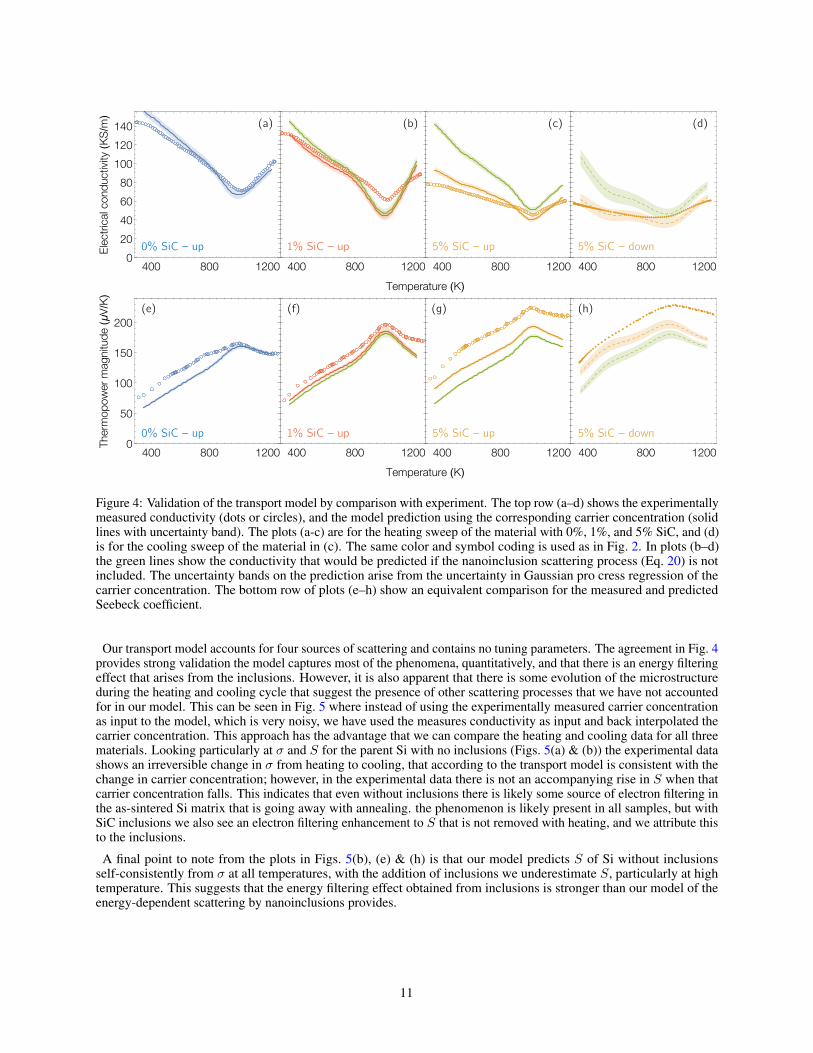
Figure 3(f) shows the electron lifetime for different scattering mechanisms in Si at 500 K with a carrier populationof 2.8× 10²⁰ 1/cm3. In the parent Si, impurity scattering is dominant across the whole energy spectrum. However,scattering from inclusions has a stronger energy dependence than impurity scattering, and so the addition of inclusionscreates a range of low energy states for which inclusion scattering is dominant. This fulfills the strategy for electronenergy filtering illustrated in Fig. 3(a)-(b). This is important as it shows that unequivocally the enhancement in theSeebeck coefficient in the experiments is at least partially due to the filtering effect. Moreover, the lifetimes plottedin Fig. 3(f) indicate that the additional grain boundary scattering rate is nearly two orders of magnitude weaker thanthat required to explain the experimental results (Fig. 2). The conclusion that grain boundaries are not influencingthe Seebeck coefficient is also constant with other works in the literature [52]. Figure 4 shows the comparison ofthe experimentally measured σ and S with the predictions from the model using the fits to the measured carrierconcentrations. The predictions for the electrical conductivity are in very good agreement with the experiment. Forthe material with 5% inclusions, omitting the inclusion scattering results in a significantly poorer prediction of σ. Themodel predictions for S are less good, systematically underestimate the Seebeck coefficient by around 10%. TheSeebeck coefficient is highly sensitive to the band curvature and so we speculate that our model’s underprediction of Sstems from the limitation in using a single band approximation to accurately represent the energy states in the wholeBrillouin zone – see for instance [49]. Nonetheless, the model predicts the correct overall trends in S between thedifferent nanocomposites, and it can again be seen that the predictions are worse if inclusion scattering is omitted.
10
(μ/)
()
(/)
()
(a) (b) (c) (d)
(e) (f) (g) (h)
0% SiC – up 1% SiC – up 5% SiC – up 5% SiC – down
0% SiC – up 1% SiC – up 5% SiC – up 5% SiC – down
Figure 4: Validation of the transport model by comparison with experiment. The top row (a–d) shows the experimentallymeasured conductivity (dots or circles), and the model prediction using the corresponding carrier concentration (solidlines with uncertainty band). The plots (a-c) are for the heating sweep of the material with 0%, 1%, and 5% SiC, and (d)is for the cooling sweep of the material in (c). The same color and symbol coding is used as in Fig. 2. In plots (b–d)the green lines show the conductivity that would be predicted if the nanoinclusion scattering process (Eq. 20) is notincluded. The uncertainty bands on the prediction arise from the uncertainty in Gaussian pro cress regression of thecarrier concentration. The bottom row of plots (e–h) show an equivalent comparison for the measured and predictedSeebeck coefficient.
Our transport model accounts for four sources of scattering and contains no tuning parameters. The agreement in Fig. 4provides strong validation the model captures most of the phenomena, quantitatively, and that there is an energy filteringeffect that arises from the inclusions. However, it is also apparent that there is some evolution of the microstructureduring the heating and cooling cycle that suggest the presence of other scattering processes that we have not accountedfor in our model. This can be seen in Fig. 5 where instead of using the experimentally measured carrier concentrationas input to the model, which is very noisy, we have used the measures conductivity as input and back interpolated thecarrier concentration. This approach has the advantage that we can compare the heating and cooling data for all threematerials. Looking particularly at σ and S for the parent Si with no inclusions (Figs. 5(a) & (b)) the experimental datashows an irreversible change in σ from heating to cooling, that according to the transport model is consistent with thechange in carrier concentration; however, in the experimental data there is not an accompanying rise in S when thatcarrier concentration falls. This indicates that even without inclusions there is likely some source of electron filtering inthe as-sintered Si matrix that is going away with annealing. the phenomenon is likely present in all samples, but withSiC inclusions we also see an electron filtering enhancement to S that is not removed with heating, and we attribute thisto the inclusions.
A final point to note from the plots in Figs. 5(b), (e) & (h) is that our model predicts S of Si without inclusionsself-consistently from σ at all temperatures, with the addition of inclusions we underestimate S, particularly at hightemperature. This suggests that the energy filtering effect obtained from inclusions is stronger than our model of theenergy-dependent scattering by nanoinclusions provides.
11

()
(/)
()
(μ/)
-
()
(
/
)
()
(/)
()
(μ/)
-
()
(
/
)
-
()
(/)
()
(μ/)
-
()
(
/
)
(a) (b) (c)
(d) (e) (f)
(g) (h) (i)
0% S
iCin
clus
ions
1% S
iCin
clus
ions
5% S
iCin
clus
ions
Figure 5: Predictions of the transport model working backward from the experimentally measured electrical conductivity.The top, middle, and bottom rows show the measured data from both the heating and cooling sweeps for the materialwith 0%, 1%, and 5% volume fraction of SiC respectively. Plots in the left column (a, d, g) show the measuredelectrical conductivity (blue) and the conductivity predicted by the transport model using the raw (unsmoothed) carrierconcentration measurement data (red). Open and closed circles are used to distinguish the data from the heating andcooling sweeps, respectively. Plots in the central column (b, e, h) show the magnitude of the experimentally measuredSeebeck coefficient (blue), and its prediction using the carrier concentration that is obtained from the transport modelby back interpolation from the experimentally measured conductivity (red). The plots in the right-hand column (c, f, i)show the raw experimental carrier concentration (blue), and the carrier concentration predicted by back interpolationfrom the experimentally measured conductivity (red). In the second two rows, data plotted in green is the modelprediction if the inclusion scattering term is omitted.
6 MAXIMUM THEORETICAL POWER FACTOR ENHANCEMENT OBTAINABLEFROM ENERGY FILTERING
In the prior sections, we have validated our transport model and used it to demonstrate that SiC inclusions in Siprovide an energy filtering effect. Here we extend the use of the transport model to examine how much scope existsfor improving the power factor of Si nanocomposites if one were able to engineer inclusions or some other scattering
12

mechanism that provides ideal filtering. The approach of electron energy filtering is to shift the transport distribution’scenter of mass by tuning τ – in essence, blocking or filtering low energy electrons so that they do not contribute totransport. The concept has the practical advantage that it is easier to add extrinsic sources of scattering to the materialthan it is to tune the material’s band structure. However, typically one can only add sources of electrical scattering whichmeans that, as with tuning χ, enhancement of S, is obtained at the expense of σ. This can still yield an improvement inZT providing the power factor is increased. When tuning the parameters in χ it is found that the trade-off between Sand σ leads to a narrow window of optimal conditions that maximize the power factor. However, as we demonstratebelow, no such trade-off exists when tuning τ . Electron energy filtering can always be made to increase S2 more quicklythan σ, enabling the power factor, in theory, to be increased indefinitely.
6.1 Cutoff Model – Perfect Filtering
To better understand the enhancement in power factor that can be obtained with the energy selective filtering we canconsider the extreme case where all the electrons with energy lower than Uo are completely blocked. For this perfectfiltering case, it is useful to evaluate the fraction of the total transport integrals in χ and γ as a function of energy abovethe conduction band edge. We call these X(E) and Γ(E) and define them as
X(E) =
∫ E0dE′χ(E′)τp(E
′)∫∞0dE′χ(E′)τp(E′)
(14)
Γ(E) =
∫ E0dE′γ(E′)τp(E
′)∫∞0dE′γ(E′)τp(E′)
(15)
The function X(E) is always positive, while Γ(E) is negative for E < EA, where EA is the energy level at which∫ Ef
0dEγ(E) = −
∫ EA
EfdEγ(E). The function Γ(E) is always less than X(E) and converges to 1 more slowly than
X(E). The integral fractions describe how much an energy range in the conduction band contributes to transport.They can be used to define, ασ(Uo), the ratio of a materials’ electrical conductivity with and without energy filtering.Similarly, we define αS(Uo) and αPF (Uo)
ασ(Uo) = 1−X(Uo) (16)
αS(Uo) =1− Γ(Uo)
1−X(Uo)(17)
αPF (Uo) =(1− Γ(Uo))
2
1−X(Uo)(18)
The power factor enhancement, αPF (Uo), always rises above unity for small values of Uo, but falls back below onewhen Γ(Uo) = 1−
√(1−X(Uo)). The optimum filtering threshold for power factor enhancement, U∗PF , satisfies the
condition
U∗PF = Ef −eTS
2
(1− Γ(U∗PF )
1−X(U∗PF )
)= Ef −
eTS
2αS(U∗PF ) (19)
where S is the Seebeck coefficient in the bulk material. This implies that Ef < U∗PF < EA. Figure 6(a) shows thevariation of power factor with carrier concentration for ideal electron filtering in Si as a function of energy filteringcutoff, Uo, at 500 K. This suggests that theoretically there is considerable room for further improvement to the powerfactor. More surprising is how the maximum obtainable power factor changes with carrier concentration as plotted inFig. 6(b) – it shows that if one can tune the energy filtering threshold then one should adopt a new paradigm for thedesign and optimization of thermoelectric materials. In the traditional picture of a n-type thermoelectric, the material’spower factor is maximized at carrier concentrations that place the Fermi energy at the conduction band edge. However,if one applies perfect energy filtering one can obtain a greatly enhanced power factor by doping the material so asto push the Fermi energy deeper into the conduction band — even to doping levels where thermal conductivity isdominated by electron transport. This presents a new strategy for designing thermoelectric which is freed from theconstraint of optimizing the carrier concentration.
13

σ(
/)
-(μ/)
([-])
σ(
/
/ )
-
()
- ()
σ(
/
/ )
(/)
(×
-
Ω/
)
Carrier conc. (Log10[cm-3])
Uo – E
c (eV)
Pow
er fac
tor
(mW
/m.K2 )
(a) (b)
(c) (d)300 K
500 K
1300 K
Kim modelBTE (this work)
@ 500 K
@ 500 K
@ 500 K 𝜎S
𝜎S!
EFUo
3 nm50 nm3 nm50 nmBulk
Figure 6: Plot (a) shows the variation of power factor of P-doped Si with carrier concentration as a function of theelectron perfect filtering threshold, Uo at 500 K. Panel (b) shows the model prediction of the electrical transportproperties in P-doped Si at 500 K. The top panel shows the conductivity σ (blue, left ordinate axis) and thermopowerS (red, right ordinate axis), while the bottom panel shows the power factor (purple, left ordinate) and the optimalperfect filtering threshold Uo relative to the Fermi level (green, right ordinate, solid and dashed lines respectively). Thetransport coefficients for the bulk and 5% SiC additive dispersoids are plotted in solid and dash lines, respectively. Thefilled markers are the experimentally measured quantities for the bulk Si (triangle) and Si/SiC (1% SiC in square, 5%SiC during heating in diamond and during cooling in circle) membranes. The maximum PF through ideal filtering isplotted dot-dash line. Without exploiting energy filtering there is an optimal carrier concentration for the thermoelectricpower, and the experimental materials are very close to it; however, by exploiting energy filtering it is possible tocontinue increasing the power factor by increasing the carrier concentration. The model predicts that at this temperaturethere is considerable scope for further enhancement of the power factor through ideal electron filtering. Plot (c) showsthe comparison the perfect filtering model (τo = 0 fs solid lines) and a less perfect filtering model (τo = 10 fs, dashedlines) as a function of the energy filtering threshold Uo. The carrier concentration is fixed at 1020 1/cm3, the red,orange, and yellow plots correspond to temperatures of 300, 500, and 1300 K, respectively. Shorter τo is more beneficialfor power factor enhancement, but the optimal Uo depends on temperature. Pane (d) shows the variation of Lorenz’snumber with carrier concentration for in a nanocomposite containing SiC nanoparticles with radii of 3 nm and 50 nm(dashed and dotted lines respectively). The blue lines show the prediction from Kim et al.’s model and red lines thepredictions from this work. The solid red line shows Lorenz’s number for bulk Si. The temperature is fixed at 500 K.
6.2 Generalized Cutoff Model
While the perfect cutoff model suggests an extremely large enhancement in power factor, it is not feasible to completelyblock low-energy electrons, here, we instead take a phenomenological approach. Regardless of the mechanism ofscattering, we assume that the scattering rate from inclusions is largest for low energy electrons and weaker for highenergy electrons (consistent with Fermi’s golden model of nanoparticles scattering rate). The reverse trend is true for ionscattering and so we assume that scattering of low energy electrons is dominated by scattering from inclusions but that
14
there can exist crossover energy Uo where the scattering of electrons with energy above this threshold is predominantlyfrom dopants. The filtering threshold Uo is related to the conduction band offset, ∆EC . The simplest phenomenologicalmodel of inclusion scattering is to model the additional rate of scattering as a step function so that electrons with energyE < Uo are subjected to an additional scattering process with characteristic lifetime τo, represented mathematically as
τ−1c = τ−1
o ϑ(Uo − E) (20)
where ϑ is the Heaviside function. Matthiessen’s rule is used to sum the rate of this extrinsic scattering term withelectron-impurity and electron-phonon scattering giving the total electron scattering rate. Using this scattering functionin the transport model we can examine the model’s prediction for transport properties of nanoengineered Si. Figure6(c) shows the predicted power factor for a material with the carrier concentration of n = 1020 1/cm3, for ideal cutoffmodel (τo = 0 fs) in red and generalized cutoff model (τo = 10 fs) in blue, if we could independently control Uo andτo. This provides several important insights. The first is that the optimal filtering threshold, Uo, for enhancing powerfactor is relatively independent of τo and vice versa. Figure 6(c) also shows that if the filtering threshold is not optimalelectron filtering can diminish the power factor rather than enhance it. Shorter τo is more beneficial for power factorenhancement, but the optimal Uo depends on temperature.
7 MODEL PREDICTION FOR ELECTRON THERMAL CONDUCTIVITY
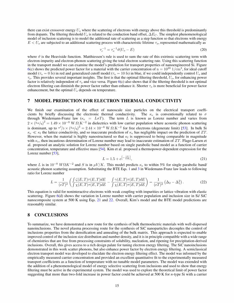
We finish our examination of the effect of nanoscale size particles on the electrical transport coeffi-cients by briefly discussing the electronic thermal conductivity. The κe is conventionally related to σthrough Wiedemann-Franz law (κe = LσT ). The term L is known as Lorenz number and varies from2× (kB/q)
2= 1.49× 10⁻⁸ W.Ω.K−2 in dielectrics with low carrier population where acoustic phonon scattering
is dominant, up to π2/3× (kB/q)
2= 2.44× 10⁻⁸ W.Ω.K−2 for free electrons (degenerate limit) [53]. In bulk Si
κe κl the lattice conductivity, and so inaccurate prediction of κe has negligible impact on the prediction of ZT .However, when the material is highly nanostructured so that κl is suppressed to being comparable in magnitudewith κe, then incautious determination of Lorenz number may lead to inaccurate estimation of ZT . Flage-Larsen etal. proposed an analytic solution for Lorenz number based on single parabolic band model as a function of carrierconcentration, temperature and effective mass [54]. Kim et al. proposed a thermopower-dependent expression for theLorenz number [53],
L = 1.5 + e[−|S|116 ], (21)
where L is in 10−8 WΩK−2 and S is in µV/K. This model predicts κe to within 5% for single parabolic band/acoustic phonon scattering assumption. Substituting the BTE Eqs. 1 and 3 in Wiedemann-Franz law leads to followingratio for Lorenz number
L =1
(eT )2
(∫ζ(E, T )τ(E, T )dE∫χ(E, T )τ(E, T )dE
−∫γ(E, T )τ(E, T )dE∫χ(E, T )τ(E, T )dE
)=
1
(eT )2
(∆2 −∆2
1
). (22)
This equation is valid for noninteractive electrons with weak coupling with impurities or lattice vibration with elasticscattering. Figure 6(d) shows the variation in Lorenz number with carrier population and inclusion size in Si/ SiCnanocomposite system at 500 K using Eqs. 21 and 22. Overall, Kim’s model and the BTE model predictions arereasonably similar.
8 CONCLUSIONS
To summarize, we have demonstrated a new route for the synthesis of bulk thermoelectric materials with well-dispersednanoinclusions. The novel plasma processing route for the synthesis of SiC nanoparticles decouples the control ofinclusions properties from the densification and annealing of the bulk matrix. This approach is expected to enableimproved control of the inclusion size distribution and number density, and it is in principle compatible with a wide rangeof chemistries that are free from processing constraints of solubility, nucleation, and ripening for precipitation-derivedinclusions. Overall, this gives access to a rich design palate for tuning electron energy filtering. The SiC nanoinclusionsdemonstrated in this work scatter phonons, but also enhance power factor by electron energy filtering. A semiclassicalelectron transport model was developed to elucidate the electron energy filtering effect. The model was informed by theempirically measured carrier concentration and provided an excellent quantitative fit to the experimentally measuredtransport coefficients as a function of temperature with no tunable model parameters. The model was extended withthe addition of a phenomenological model of energy selective scattering from inclusions and used to show that energyfiltering must be active in the experimental system. The model was used to explore the theoretical limit of power factorsuggesting that more than two-fold increase in power factor could be achieved at 500 K for n-type Si with a carrier
15
concentration ∼ 3× 10²⁰ 1/cm3. More remarkable, is that the theoretical maximum obtainable power factor usingelectron energy filtering continues to rise monotonically with increasing carrier concentration, substantially altering theconstraint imposed by carrier concentration on the design of thermoelectric materials.
9 ACKNOWLEDGEMENTS
Authors DC and LM were supported by the National Science Foundation under grant 1351386. Part of this workwas performed at the California Institute of Technology/Jet Propulsion Laboratory under contract with the NationalAeronautics and Space Administration and was support-ed by the NASA Science Missions Directorate’s RadioisotopePower Systems Program.
10 DATA AVAILABILITY
The raw data from these measurements and calculations is available upon request from the corresponding authors.
11 CONFLICT OF INTEREST
The authors declare no conflict of interest.
References
[1] S Aria Hosseini, Giuseppe Romano, and P Alex Greaney. Mitigating the effect of nanoscale porosity onthermoelectric power factor of si. ACS Applied Energy Materials, 4(2):1915–1923, 2021.
[2] Jinyao Tang, Hung-Ta Wang, Dong Hyun Lee, Melissa Fardy, Ziyang Huo, Thomas P Russell, and Peidong Yang.Holey silicon as an efficient thermoelectric material. Nano letters, 10(10):4279–4283, 2010.
[3] Chhatrasal Gayner and Yaron Amouyal. Energy filtering of charge carriers: Current trends, challenges, andprospects for thermoelectric materials. Advanced Functional Materials, 30(18):1901789, 2020.
[4] Yi Ma, Richard Heijl, and Anders EC Palmqvist. Composite thermoelectric materials with embedded nanoparticles.Journal of Materials Science, 48(7):2767–2778, 2013.
[5] S Aria Hosseini, Sarah Khanniche, P Alex Greaney, and Giuseppe Romano. Universal effective medium theory topredict the thermal conductivity in nanostructured materials. International Journal of Heat and Mass Transfer,183:122040, 2022.
[6] S Aria Hosseini, Giuseppe Romano, and P Alex Greaney. Enhanced thermoelectric performance of polycrystallinesi0. 8ge0. 2 alloys through the addition of nanoscale porosity. Nanomaterials, 11(10):2591, 2021.
[7] Laura de Sousa Oliveira, S Aria Hosseini, Alex Greaney, and Neophytos Neophytou. Heat current anticorrelationeffects leading to thermal conductivity reduction in nanoporous si. Physical Review B, 102(20):205405, 2020.
[8] Laura de Sousa Oliveira and Neophytos Neophytou. Large-scale molecular dynamics investigation of geometricalfeatures in nanoporous si. Physical Review B, 100(3):035409, 2019.
[9] Sabah K Bux, Richard G Blair, Pawan K Gogna, Hohyun Lee, Gang Chen, Mildred S Dresselhaus, Richard BKaner, and Jean-Pierre Fleurial. Nanostructured bulk silicon as an effective thermoelectric material. AdvancedFunctional Materials, 19(15):2445–2452, 2009.
[10] Jackson R Harter, S Aria Hosseini, Todd S Palmer, and P Alex Greaney. Prediction of thermal conductivity indielectrics using fast, spectrally-resolved phonon transport simulations. International Journal of Heat and MassTransfer, 144:118595, 2019.
[11] HR Shanks, PD Maycock, PH Sidles, and GC Danielson. Thermal conductivity of silicon from 300 to 1400 k.Physical Review, 130(5):1743, 1963.
[12] D Coleman, T Lopez, S Exarhos, M Mecklenburg, S Bux, and L Mangolini. Thermoelectric performance ofsilicon with oxide nanoinclusions. Materials Research Letters, 6(8):419–425, 2018.
[13] Thomas Lopez and Lorenzo Mangolini. In situ monitoring of hydrogen desorption from silicon nanoparticles dis-persed in a nonthermal plasma. Journal of Vacuum Science & Technology B, Nanotechnology and Microelectronics:Materials, Processing, Measurement, and Phenomena, 34(4):041206, 2016.
16

[14] Uwe R Kortshagen, R Mohan Sankaran, Rui N Pereira, Steven L Girshick, Jeslin J Wu, and Eray S Aydil.Nonthermal plasma synthesis of nanocrystals: fundamental principles, materials, and applications. Chemicalreviews, 116(18):11061–11127, 2016.
[15] Marc K Etherington, Nadzeya A Kukhta, Heather F Higginbotham, Andrew Danos, Aisha N Bismillah, David RGraves, Paul R McGonigal, Nils Haase, Antonia Morherr, Andrei S Batsanov, et al. Persistent dimer emission inthermally activated delayed fluorescence materials. The Journal of Physical Chemistry C, 123(17):11109–11117,2019.
[16] CA Swenson. Recommended values for the thermal expansivity of silicon from 0 to 1000 k. Journal of physicaland chemical reference data, 12(2):179–182, 1983.
[17] Kasper A Borup, Eric S Toberer, Leslie D Zoltan, George Nakatsukasa, Michael Errico, Jean-Pierre Fleurial, Bo BIversen, and G Jeffrey Snyder. Measurement of the electrical resistivity and hall coefficient at high temperatures.Review of Scientific Instruments, 83(12):123902, 2012.
[18] C Wood, D Zoltan, and G Stapfer. Measurement of seebeck coefficient using a light pulse. Review of scientificinstruments, 56(5):719–722, 1985.
[19] G Jeffrey Snyder and Eric S Toberer. Complex thermoelectric materials. In Materials for sustainable energy: acollection of peer-reviewed research and review articles from Nature Publishing Group, pages 101–110. WorldScientific, 2011.
[20] Xin Guan and Jianyong Ouyang. Enhancement in the seebeck coefficient of organic thermoelectric materialsthrough energy filtering of charge carriers. CCS Chemistry, pages 1–37, 2021.
[21] Anh Tuan Thanh Pham, Phuong Thanh Ngoc Vo, Hanh Kieu Thi Ta, Hoa Thi Lai, Vinh Cao Tran, Tan Le HoangDoan, Anh Tuan Duong, Ching-Ting Lee, PK Nair, Yohandys A Zulueta, et al. Improved thermoelectric powerfactor achieved by energy filtering in zno: Mg/zno hetero-structures. Thin Solid Films, 721:138537, 2021.
[22] Je-Hyeong Bahk, Zhixi Bian, and Ali Shakouri. Electron transport modeling and energy filtering for efficientthermoelectric mg2si1−xsnx solid solutions. Phys. Rev. B, 89:075204, Feb 2014.
[23] Je-Hyeong Bahk, Zhixi Bian, and Ali Shakouri. Electron energy filtering by a nonplanar potential to enhance thethermoelectric power factor in bulk materials. Phys. Rev. B, 87:075204, Feb 2013.
[24] Aaron J Schmidt, Kimberlee C Collins, Austin J Minnich, and Gang Chen. Thermal conductance and phonontransmissivity of metal–graphite interfaces. Journal of Applied Physics, 107(10):104907, 2010.
[25] Gang Chen. Nanoscale energy transport and conversion: a parallel treatment of electrons, molecules, phonons,and photons. Oxford University Press, 2005.
[26] T. J. Scheidemantel, C. Ambrosch-Draxl, T. Thonhauser, J. V. Badding, and J. O. Sofo. Transport coefficientsfrom first-principles calculations. Phys. Rev. B, 68:125210, Sep 2003.
[27] Mark S Lundstrom and Changwook Jeong. Near-Equilibrium Transport: Fundamentals and Applications,volume 2. World Scientific Publishing Company, 2012.
[28] Y Pei, AD LaLonde, H Wang, and G Jeffrey Snyder. Energy environ. sci. 5, 7963 (2012).[29] S. Aria Hosseini. Thermoelectric.py. https://github.com/ariahosseini/thermoelectric.py, 2019.[30] G. Kresse and J. Furthmüller. Efficient iterative schemes for ab initio total-energy calculations using a plane-wave
basis set. Phys. Rev. B, 54:11169–11186, Oct 1996.[31] G Kresse and J Hafner. Phys. re v. b 1993, 47, 558.(b) kresse, g.; furthmüller. Comput. Mater. Sci, 6:15, 1996.[32] G. Kresse and J. Hafner. Ab initio molecular-dynamics simulation of the liquid-metal–amorphous-semiconductor
transition in germanium. Phys. Rev. B, 49:14251–14269, May 1994.[33] Georg Kresse and Jürgen Hafner. Ab initio molecular dynamics for liquid metals. Physical Review B, 47(1):558,
1993.[34] John P Perdew, Kieron Burke, and Matthias Ernzerhof. Generalized gradient approximation made simple. Physical
review letters, 77(18):3865, 1996.[35] Georg Kresse and Daniel Joubert. From ultrasoft pseudopotentials to the projector augmented-wave method.
Physical review b, 59(3):1758, 1999.[36] Peter E Blöchl. Projector augmented-wave method. Physical review B, 50(24):17953, 1994.[37] Hendrik J Monkhorst and James D Pack. Special points for brillouin-zone integrations. Physical review B,
13(12):5188, 1976.[38] Mark Lundstrom. Fundamentals of carrier transport. Cambridge university press, 2009.
17
[39] Michael E Levinshtein, Sergey L Rumyantsev, and Michael S Shur. Properties of Advanced SemiconductorMaterials: GaN, AIN, InN, BN, SiC, SiGe. John Wiley & Sons, 2001.
[40] M Mondal and KP Gnatak. Effect of carrier degeneracy on the screening length in degenerate tetragonalsemiconductors. physica status solidi (b), 135(1):239–251, 1986.
[41] D Mark Riffe. Temperature dependence of silicon carrier effective masses with application to femtosecondreflectivity measurements. JOSA B, 19(5):1092–1100, 2002.
[42] Yu I Ravich, BA Efimova, and VI Tamarchenko. Scattering of current carriers and transport phenomena in leadchalcogenides. physica status solidi (b), 43(1):11–33, 1971.
[43] M. V. Fischetti. Monte carlo simulation of transport in technologically significant semiconductors of the diamondand zinc-blende structures. i. homogeneous transport. IEEE Transactions on Electron Devices, 38(3):634–649,1991.
[44] Hohyun Lee, Daryoosh Vashaee, DZ Wang, Mildred S Dresselhaus, ZF Ren, and Gang Chen. Effects of nanoscaleporosity on thermoelectric properties of sige. Journal of Applied Physics, 107(9):094308, 2010.
[45] Biswaranjan R Nag. Electron transport in compound semiconductors, volume 11. Springer Science & BusinessMedia, 2012.
[46] Seyed Aria Hosseini. Prediction of Thermal and Electrical Transport in Nanostructured Materials for EnergyConversion Applications. PhD thesis, University of California, Riverside, 2021.
[47] J Martin, Li Wang, Lidong Chen, and GS Nolas. Enhanced seebeck coefficient through energy-barrier scatteringin pbte nanocomposites. Physical review B, 79(11):115311, 2009.
[48] A. J. Minnich, H. Lee, X. W. Wang, G. Joshi, M. S. Dresselhaus, Z. F. Ren, G. Chen, and D. Vashaee. Modelingstudy of thermoelectric sige nanocomposites. Phys. Rev. B, 80:155327, Oct 2009.
[49] AJ Minnich, H Lee, XW Wang, G Joshi, MS Dresselhaus, ZF Ren, G Chen, and D Vashaee. Modeling study ofthermoelectric sige nanocomposites. Physical Review B, 80(15):155327, 2009.
[50] Guangsha Shi and Emmanouil Kioupakis. Electronic and optical properties of nanoporous silicon for solar-cellapplications. Acs Photonics, 2(2):208–215, 2015.
[51] M Cruz, C Wang, MR Beltrán, and J Tagüeña-Martínez. Morphological effects on the electronic band structure ofporous silicon. Physical Review B, 53(7):3827, 1996.
[52] M. Bachmann, M. Czerner, and C. Heiliger. Ineffectiveness of energy filtering at grain boundaries for thermoelec-tric materials. Phys. Rev. B, 86:115320, Sep 2012.
[53] Hyun-Sik Kim, Zachary M Gibbs, Yinglu Tang, Heng Wang, and G Jeffrey Snyder. Characterization of lorenznumber with seebeck coefficient measurement. APL materials, 3(4):041506, 2015.
[54] E Flage-Larsen and Ø Prytz. The lorenz function: Its properties at optimum thermoelectric figure-of-merit.Applied Physics Letters, 99(20):202108, 2011.
18