Next-Generation Memory Interfaces Capstone Report · PDF fileElectrical Engineering and...
51
Next-Generation Memory Interfaces Capstone Report Kyle Dillon Electrical Engineering and Computer Sciences University of California at Berkeley Technical Report No. UCB/EECS-2015-104 http://www.eecs.berkeley.edu/Pubs/TechRpts/2015/EECS-2015-104.html May 14, 2015
Transcript of Next-Generation Memory Interfaces Capstone Report · PDF fileElectrical Engineering and...

Next-Generation Memory Interfaces Capstone Report
Kyle Dillon
Electrical Engineering and Computer SciencesUniversity of California at Berkeley
Technical Report No. UCB/EECS-2015-104http://www.eecs.berkeley.edu/Pubs/TechRpts/2015/EECS-2015-104.html
May 14, 2015

Copyright © 2015, by the author(s).All rights reserved.
Permission to make digital or hard copies of all or part of this work forpersonal or classroom use is granted without fee provided that copies arenot made or distributed for profit or commercial advantage and thatcopies bear this notice and the full citation on the first page. To copyotherwise, to republish, to post on servers or to redistribute to lists,requires prior specific permission.

!
University of California, Berkeley College of Engineering
MASTER OF ENGINEERING - SPRING 2015
Electrical Engineering and Computer Science
Integrated Circuits
Next-Generation Memory Interfaces Capstone Report
Kyle Dillon
This Masters Project Paper fulfills the Master of Engineering degree requirement.
Approved by:
1. Capstone Project Advisor:
Signature: __________________________ Date ____________
Print Name/Department: Elad Alon/EECS
!!2. Faculty Committee Member #2:
Signature: __________________________ Date ____________
Print Name/Department: Vladimir Stojanovic/EECS
!

Next%Generation,Memory,Interfaces,Capstone,Report,Abstract,Kyle,Dillon,!
Next&generation!DDR4!memory!has!significantly!improved!performance!and!energy!consumption!over!previous&generation!DDR3!technology.!!However,!this!increase!in!performance!and!decrease!in!energy!has!resulted!in!a!variety!of!design!challenges!for!peripheral!circuitry.!This!paper!focuses!on!the!physical!interface!for!DDR4!memory.!!The!physical!interface!is!the!interface!over!which!the!processor!communicates!with!the!memory.!
This!paper!consists!of!three!main!sections:!industry!analysis,!intellectual!property!strategy,!and!technical!contribution.!A!market!analysis!of!the!memory!integrated!circuits!industry!in!presented!in!the!industry!analysis!section.!In!the!IP!strategy!section,!the!different!options!for!a!physical!interface!IP!are!considered!and!compared.!Finally,!in!the!technical!contributions!section,!a!research!summary!of!my!personal!research!on!DDR4!is!presented.!Also,!a!variety!of!serializer!(one!of!the!essential!circuit!blocks!of!the!physical!interface)!designs!are!compared!and!a!preferred!design!is!chosen!to!be!integrated!into!the!physical!interface.!The!other!circuit!blocks!that!make!up!the!collaboratively!designed!physical!interface!are!discussed!in!greater!detail!in!their!respective!Capstone!reports.!

Next-Generation Memory Interfaces Capstone Report
Kyle Dillon
May 15th, 2015

! 1!
Table of Contents
Project Context and Introduction 2 Industry, Market, and Trends Analysis 3 IP Strategy 16 Technical Contribution: Serializer 21 Conclusion and Reflection 36 Bibliography 38 Appendix 42

! 2!
Project Context and Introduction
As a team we designed and tested the physical interface (PHY) for DDR4
memory. Our PHY design is to be used by the Berkeley Wireless Research Center
(BWRC) in future research projects. The PHY is an essential circuit block that facilitates
the communication between a memory controller and the DDR4 memory itself. Figure 1
illustrates where the PHY exists in a typical computer’s data flow.
Figure 1 – Simplified flow diagram of data between the processor and memory in a typical computer system.
DDR4 is the latest generation of high-speed Dynamic Random Access Memory
(DRAM). DRAM is used widely in nearly every modern computer system including
laptops, desktops, smartphones, and servers. DDR4 is faster and more energy efficient
than it’s predecessors, and it’s crucial that BWRC leverage this technology in their
research. Our PHY block is an integral part in enabling the use of DDR4.
The PHY has been divided into five separate circuit blocks, two digital blocks and
three analog blocks. The digital blocks have been designed and verified through place
and route. The analog blocks have been modeled in VerilogA and circuits have been
designed that fit these models. Furthermore, we designed the circuits using an educational
32nm/28nm technology. As such, we have not designed the PHY to tape-out and it will
not be manufactured. However, the IP (Verilog source code and circuits) are provided to
BWRC so that they are able to develop the circuits in a usable technology if desired.

! 3!
We’ve integrated all blocks into Cadance as individual circuit blocks and wrapped
them in a top-level test infrastructure to verify that all blocks communicate properly with
one another. For more information regarding the different circuit blocks, see the
Technical Contribution section of this paper.
This paper consists of an industry and market analysis for the
semiconductor/memory industry, an IP strategy including the possibility for a patent, and
my personal technical contributions to the project.
Industry, Market and Trends Analysis
In this section we will investigate the current semiconductor industry, what
technologies exist and how our technology fits, and elaborate on the current competitive
landscape of the market. We will also establish our possible clients, stakeholders, and our
go-to-market strategy. Finally, we will evaluate the current social, technological, and
economic trends and how these forces affect the industry.
Integrated circuits are an important sector in the semiconductor industry. The
semiconductor industry is known to be highly competitive in nature, and the trend has
been increasing over the years (Ulama 2014:19). Product life cycles are short, as more
technologically advanced products replace older ones. Adoption of products is majorly
affected by performance and reliability. The notable companies in the integrated circuits
industry are Intel Corporation and Samsung Electronics with 7.6% and 5.3% of the global
semiconductor and electronics parts manufacturing market, respectively (IBISWorld
2015: 27). Broadcom Corporation, Texas Instruments Inc., Advanced Micro Devices
(AMD) Inc., Micron Technology Inc. are a few of the other major companies that
compete in this industry (Ulama 2014:19). The major companies in this industry are all

! 4!
fairly large and well established, and compete over products and technologies. High
demand for products and extremely low pricing intensify the competition in the industry.
This poses a significant barrier to entry for new and smaller companies leading to only
several companies currently building DDR4 memory chips and controllers. In fact,
Micron and Samsung is the only one of the large integrated circuits companies listed
above that develops DRAM technology.
As we strive to make a smaller, faster, and more efficient memory interface, we
have to compete with the products, research and development efforts of competing
companies. Our competitive landscape does not merely include semiconductor
companies, but also technologies that have similar features and functions when compared
against our project. Existing memory technologies, such as DDR3, 3D stacked (3DS) -
DDR3, and GDDR4, compete with DDR4 on various parameters such as cost, speed, and
use-cases. While DDR4 is faster than previous memory generations, the higher cost of
the new chip technology would make the cheaper DDR3 technology a strong competitor.
Emphasis is placed on the significant performance improvements that DDR4
presents over DDR3 technology. The following table shows a brief comparison of the key
features between two technologies.
Table 1. Comparison between DDR3 and DDR4 [1]:
DDR3 DDR4
Power supply voltage 1.5V 1.2 V
Speed 1.6~2.1 Gbps 1.6~3.2 Gbps
Density 8GB(max) 16GB(max)
Price $100 avg $200 avg.

! 5!
The first comparison is in regards to power efficiency, not only does DDR4 have a
lower supply voltage, but it also implements a new algorithm to control its energy
consumption by entering its “standby” mode more frequently and precisely than DDR3.
The improvements lead to better performance in both the power consumption, and
operating temperature.
Furthermore, the most essential feature, memory speed, has been improved
significantly in DDR4. The analogy between the memory speed and highway traffic
speed is very descriptive. The speed of the memory is the amount of data can be
transferred in a certain period of time. There are two factors determining the speed, which
are interface width (the number of parallel wires in the interface) and frequency of the
memory’s operation. Considering the analogy, the bandwidth is the quantity of lanes on a
highway, and frequency is the travel speed of its vehicles. Within a fixed time period,
having more lines and a faster speeds will allow for more vehicles to travel. Similarly,
having an improved working frequency, along with an enlarged bandwidth, DDR4
achieves a data transmission speed that is approximately 1.5 times faster than DDR3, as
Table 1 indicates. The increase of the speed is benefited from the revolutionary bank-
group management technology.
Another differentiating factor is the density, or say, the space of a single memory
chip. Advancements in the chip’s encapsulation provide DDR4 a 50% density increase,
with regard to maximum space. With a larger storage space, DDR4 is able to process
more information simultaneously. However, similar to every emerging new technology,
the current price of DDR4 memory is 30% to 50% more expensive than DDR3, which
can achieve similar functionality at lower speeds. With a large-scale adaptation for DDR4

! 6!
memory, and hardware compatibility of its peripheral devices, the manufacture price
would quickly become more affordable in the future.
The GDDR3 and GDDR5, which stands for Graphics Double Data Rate, are a
kind of memory specifically designed for image processing. Despite the similarity in
terms of the name, the graphic memory is named one generation ahead regular memory.
This means that the core technology of GDDR3 is essentially an upgraded version based
on DDR2 technology, rather than DDR3. The graphic memory is designed to have lower
energy consumption, and an optimized performance when dealing with graphical-data
processing. Since the application area of these two kinds memory differentiates amongst
each other, they do not compete directly. The Graphic DDR is typically developed based
on the previous generation of DDR memory technology, with improvements on speed
and application-specific functional modifications.
As for the market analysis of our product, the main markets include traditional
memory devices and consumer electronics - and they are booming. Based on
transparency market research, it states that the global next generation memory
technologies market (only considering new memory technologies) was worth $207.8
million in 2012, and is projected to be worth $2,837.0 million by 2019, growing at a
46.1% average growth rate from 2013 to 2019 (Transparency Market Research, 2014).
The report divides the overall market for next generation memory technologies on the
basis of certain parameters: interface type, application, and geography. On the basis of
interface, the market for next generation memory technologies can be categorized into
SATA, SAS, DDR, and PCIe and I2C (Transparency Market Research, 2014). The main

! 7!
applications of next generation memory technologies include embedded MCU and smart
card, mobile phones, mass storage, cache memory, enterprise storage, and automotive.
Geographically, the global next generation memory technologies’ markets can be
divided into North America, Europe, Asia-Pacific, and the rest of the world. This industry
is always looking for ways to decrease power consumption, increase density, and develop
clever architectures. The new generation memory technologies market has gained
significant momentum in recent years due to growing demand for faster, highly scalable,
and cost-effective memory solutions.
Understanding the necessity of our effort follows from understanding the
industry dynamic, which our product tempts to enter. After understanding the landscape
within which we stand, we remain to have reason to believe that our project is valuable to
our stakeholders. We remain to reason that our stakeholders should be more interested in
receiving a completed deliverable from us over any other, equally qualified, external
competitor.
Our first differentiating quality is that we offer to provide “non-contracted” work.
Contracted work is any work commissioned by one party to be executed by another party.
To begin such work, both parties must agree on the terms defined within the agreement
document prior to the work’s commencement. The agreement is realized through means
of a binding contract that both parties agree to enact. Once the contract is created, it
typically cannot be altered or modified, unless the consent of all parties is evident. This
could place the requesting party into a stiff situation if it discovers that its priorities have
changed mid-way through a contract.

! 8!
Upon the project’s completion, the completed work is commonly handed off “as-
is.” This means that no additional support is to be provided in the future (unless explicitly
negotiated upon within the original contract). Any additional requested support or
modification requires for a new contract to be written. Not only is this financially
inconvenient, but it can also be logistically inconvenient for the recipient. Without
support, the deliverable is handed off with a decreased utility. The recipient of the
deliverable is stuck with using the deliverable solely within its original scope.
Our stakeholder, BWRC, benefits from ownership over the development process.
A common clause added to most contractual work instills a limit on interim design
modification requests. This clause exists to prevent the requesting party from
overexerting the contracted party without compensation. Internal control over the
developmental process allows for precise design-source malleability during development,
and full exposure of the design files. Design-source malleability allows for the BWRC
professors to more closely guide our direction through the project’s development. It
allows for them to change the path that we follow if new interests arise. There is no
contractual overhead to worry about in this scenario.
BWRC benefits from retaining access, and owning, the source code and designs.
The design-source exposure enables BWRC to question every aspect of the
implementation until they understand it completely. With contracted work, this
information is typically unavailable to the requesting party due to trade secrets being used
in a design. Owning the source enables BWRC to have permanent design-source access.
Long-term source access enables cost-effective and effort-effective technology adaptation

! 9!
into any future BWRC projects. Along with adaptation, owning the source creates the
opportunity for growing in-house expertise at BWRC through education.
The benefits mentioned above align very closely with our stakeholder’s interests.
The stakeholder, being BWRC, is interested in three main attributes from the project.
First, BWRC wants a fully customizable deliverable due to unpredictable future
demands. Second, BWRC wants the freedom to optimize the design for unique
implementations that would require the modification of the source on a per-use basis.
Third, BWRC wants to avoid the financial, temporal, and contractual overheads
associated with third-party work. Our project delivers on all three attributes. By choosing
to complete this project through our team, rather than a team of contractors, BWRC
satisfies its internal interests.
Our team anticipates BWRC’s decision to work with us as opposed to larger
suppliers. The current semiconductor marketplace is saturated with both customers and
suppliers. As Ulama describes (Ulama 2014:28), “Established operators in this industry
have been able to develop solid relationships with customers, and it can be extremely
difficult for new companies to gain contracts with customers when existing
semiconductor manufacturing operators have built reputations over a long period.” To
exemplify the significance and the weight carried by the previous statement, note that the
Semiconductor and Circuit Manufacturing industry is one of the largest exporting
industries in the United States (Ulama 2014:5). It indirectly provides jobs to 250,000
Americans, is currently valued at $79.5 billion, and has grown at an annual rate of 4.8%
(Ulama 2014:5).
! 10!
The current players, both customers and producers, are very well established, and
very tightly connected. Penetrating into the customer base that the massive producers
currently support is near impossible for a small team like ours due to lack of reputation.
Aside from penetrating, the customers in this segment of the market are a significantly
strong force due to two reasons: 1. The intrinsic competitiveness of the current suppliers,
and 2. “The electronics marketplace is continually under pressure to improve product
functionality, decrease size, increase speed, and decrease cost.” (IBISWorld Global
Semiconductor & Electronic Parts 2015:33)
Our team has set our target in a completely different direction. Instead of focusing
on the massive customers, who are already served very competitively, we direct our focus
at an interestingly under-served segment in this market space. In part, our choice of
direction is due to the methods through which our Capstone project was decided upon.
The decision process confined the scope of the project to target academic goals and
provide solutions for academic institutions. Thus, our customer space currently only
encompasses the Berkeley Wireless Research Center, but is functionally able to serve any
academic or small-scale organizations.
As we currently stand, with one effective customer in our sights, we are
subjecting ourselves to a very strong customer market force. This is an undesirable
outcome due to the limited size of the space, which we choose to attack, but success in
this space will send positive signals at other research institutions. We would be able to
expand to encompass more academic institutions because they would prefer to acquire
the product through us. Our effective results are comparable to their current methods of

! 11!
operation, but with the benefit of reduced fixed-cost expenditures – which arise when
placing orders with large design and manufacture firms.
A majority of the market belongs to other companies, most all companies are well
establish large corporations including Micron (IBISWorld 2015: 27) and Texas
Instruments (IBISWorld 2015: 30). The barriers that cause this include “access to latest
technology and intellectual property, the level of investment…, access to skilled
employees, and the dominance of existing players” (IBISWorld 2015: 25). In the memory
industry, the companies compete over a very specific set of criteria including price,
performance, features and power consumption, all of which are highly measurable and
quantifiable metrics (IBISWorld 2015: 24).
If the dimensions of competition between companies in a given industry
converge, then the companies are left to compete solely on price (Porter 2008: 12). In the
integrated circuit market, the industry has converged heavily on these metrics of
performance, features and power consumption, which has resulted in fierce price
competition. Because “economies of scale can be significant in this industry” (IBISWorld
2015: 25), new entrants must manufacture large volumes to stand a chance against the
bigger companies. This requires up-front capital that many smaller new entrants do not
have available. Entering the market attempting to compete on these highly competitive
dimensions would result in “zero sum competition” (Porter 2008: 13), and and would not
be a viable business strategy.
When instead of converging on the same dimensions, companies target different
segments of the customer base, the result can be “positive sum” competition: competition
that increases the profitability of all companies (Porter 2008: 13). We plan to employ this

! 12!
strategy with our DDR4 memory controller. We’ve learned from BWRC that their needs
are different than the typical semiconductor customer. BWRC fabricates chips in low
volumes, so price is not a significant factor. Also, they require only a subset of the
industry-standard feature set for DDR4 memory controllers, enabling us to reduce the
size of the design. Finally, they need very specific portions of the controller designed, not
the entire IP block that most competitors would offer.
Although the memory technology industry is highly competitive, growing, and
difficult to penetrate, the market is growing fast due to this a demand for consumer
electronics, an industry which is expected to grow 5.3% annually to nearly $300 billion
dollars by 2019 (IBISWorld 2014: 4). This high demand and new market bring some
space for new companies to enter and grow. These new entrants usually emerge during
the transition between the technological revolutions and each one has its own speciality.
From the year of 2002 to 2013, DDR memory industry has undergone 4
significant technological transitions, all of which are aiming at improving in three
performance aspects and achieving a denser data processing capability. As Darryle stated
in the article, the product with “high levels of performance, reliability, quality and low
levels of power consumption” (Bach,2014:6) can gain an apparent advance in the
competition of memory design industry. Being the three largest manufactures of memory
chip and developer of DDR memory technology, Samsung, Crucial (Micron) and Hynix
have already invested millions of dollars in their R&D sector to develop the new
generation DDR4 memory interface in order to reinforce their dominating market share.
Given such a giant market, other major memory designers such as Kingston keep
fastening their pace to catch up the memory controller design for the recent DDR3 to

! 13!
DDR4 transition. Besides the companies who are already in the market, there are
significant number of new companies or say, new entrants, trying to seize this
opportunity. According to the statement made by Darryle, “the latest Census data
indicates that 64.1% of operators in this industry have fewer than 20 employees” (Ulama
2014:25). The development strategy of those new entrants are highly focused on certain
features, and “specializing in a small number of product lines to serve niche markets”
(Ulama 2014:25) in order to avoid a direct competition with large companies.
Table 2. Representative new entrants in DDR4 memory development
Company Name Specialized market/feature
Century Micro INC. Small physical size & low energy consumption
Montage Technology Fast operating speed & low energy consumption
G.SKILL Enhanced gaming performance
Three unique, representative companies are provided to conduct the analysis of
the new entrant. The table 1 above shows a brief comparison of three distinguished new
entrants key product features. It indicates each new entrant is trying to gain its market
share by specializing its product from the three technical aspects mentioned in the
previous paragraph.
The Japanese based company Century has just halved the physical size of DDR4
memory in their most recent product at the year of 2014. The China-based Montage Tech
is more focusing on developing fast speed and lower power rate DDR4 memory for large
scale server use. “Less power draw means less heat and longer battery life”, which
indicates “the servers are expected to be the biggest beneficiaries of the jump to DDR4”

! 14!
(Andy, 2014:6). Meanwhile, G.SKILL put majority of its resources into developing
DDR4 memory controller with improved gaming performance. These companies are
increasingly securing their niche markets by making breakthroughs in design of the
memory controller while the major developers are still dominating the memory chip
manufacturing area.
Big companies enjoy economies of scale, making it difficult to compete with
them in manufacturing the integrated circuits (ICs). Based on the analysis of the new
entrants, in order to build immunity for our design, we plan to segment the market to
research institutes like BWRC. Their needs are different from most, and provide an
opportunity for us to develop a product that satisfies these needs better than the
competition. Since the design of our project is specifically for BWRC internal research
use, there will be no direct competition and obvious threat from these new entrants either.
The threat from other technologies is weaker, as our DDR4 interface is more
advanced than existing DDR3/GDDR5 interfaces. Therefore, we focus on developing the
intellectual property and targeting the specific needs of the academic communities. This
specific category of consumers require more customizable, and open, circuit designs at a
lower volume, a need that is unmet by the larger companies that package their circuits in
black boxes, manufacture in volume, and allow little to no customization. By segmenting
the market based on unmet needs, and our abilities to satisfy them, we hope to entrench
our position as a profitable part of the semiconductor industry.
From the perspective of semiconductor circuit design, it is a complicated process
to design a controller and integrate it with the memory chip. Therefore, our technology
suppliers include both software side and hardware suppliers. Software suppliers are those

! 15!
who provide coding languages, design platforms, and simulation tools. Hardware
suppliers are those who provide electrical specifications, datasheets, and other fabrication
characteristics relating to memory chips.
Software suppliers mainly provide programming language support. Verilog and
SystemVerilog are the two main programming languages we are using. They are
hardware description languages used to model electronic systems. They are most
commonly used in design and verification of digital circuits. Cadence, a company that
provides electronic design automation software, covers many language design platforms,
including Verilog and SystemVerilog. As an all-in-one suite, Cadence is our main
software supplier.
Hardware suppliers provide descriptive information about the memory chip
technology. Our controller is on a software level, but it will be integrated with the next
generation memory chip technology, the DDR4 technology. Each generation of memory
chips has new fabrication breakthrough. Thus, during our controller design, the latest
information about memory chips is critical, such as voltage supply of the chips and the
memory bank structure. Our hardware suppliers, such as Micron Technology, Intel Corp.,
and Samsung, are big semiconductor companies in this industry. In Semiconductor &
Circuit Manufacturing in the US Industry Report, Intel Corp. and Samsung have 18% and
13.8% market share in 2014 (Ulama 2014:4). Although they seem like our competitors
from the sales end, they also have the best research departments and technical experts in
the chip fabrication domain. Samsung competes in the Semiconductor and Circuit
Manufacturing industry via its fabrication and research and development facilities in the
United States (Ulama 2014:4). They will release the paper and datasheet of their latest

! 16!
research results about DDR4 memory chip. According to the information provided by
these large semiconductor-manufacturing companies, we are able to define the interface
and design our memory controller.
Powerful suppliers capture more of the value for themselves by charging higher
prices, limiting quality or services, or shifting costs to industry participants. As
mentioned above, Intel Corp. and Samsung are both suppliers and competitors for us. If
they limit our access to their latest technology about DDR4 memory chip, it will be hard
for us to compete with them. However, the good news is that the DDR4 memory
specification is becoming a standard, so we will be less dependent on them.
There are certain aspects that we can focus on to succeed in this capital-intensive,
and research-intensive, memory design industry. New companies are trying to explore the
market by boosting their expertise in faster-speed designs, smaller dimension layouts, and
highly customized application-specific designs. WIth increasing maturity of the DDR4
technology, the competition is becoming more fierce. This increased competition will
largely benefit the semiconductor industry’s evolution speed, as well as provide
customers with cheaper and higher efficiency devices. Our project will not only
encourage further development from competing companies and research groups, but also
benefit BWRC’s exploration of the utilization of DDR4’s capabilities.
IP Strategy
The PHY interface provides us a good opportunity for creating a patentable
intellectual property. The physical layer has been split into 5 major parts, each of which
allow for novel implementations and innovations in circuit design. As we are working at

! 17!
the cutting edge of technology, we would have to adopt non-trivial techniques to meet the
specifications for high data rates of DDR4. One or more of these implementations can
provide us a patentable IP. This section will discuss why this technology may be
patentable, the advantages and disadvantages of seeking a patent, the current state of the
semiconductor IP space, and the risks associated with not seeking a patent.
In the context of IP, creative designs and creative solutions fall cleanly under the
category of patentable assets. In essence, the purpose for securing IP is to declare
discernible ownership over a design or utility (USPTO, 2013). As an independent entity,
we can draw benefits from securing patents and owning patents. The benefits we pose to
secure range from monetary compensation to strategic industrial presence.
From a monetary perspective, owning patents allows our team to claim ownership
to a recognizable asset. After incorporating our team as a legal entity, a patent opens us to
the opportunity of being acquired. The proceeds from an acquisition could be used to
finance additional ventures, which our team currently does not have the financial freedom
to pursue.
A secondary monetization strategy that patent ownership affords us, is the option
to license our technology to independent entities who wish to avoid committing R&D
expenses for the purpose of developing said technology independently. Aside from the
legal expense that we would need to undertake, the licensing option is financially robust.
The third and final benefit is an unquantifiable benefit. The third benefit arises
from establishing a reputation as an entity. Acquiring a patent will demonstrate that we,
as a team, know how to drive concepts into patentable ideas, and patentable ideas into
awarded patents. Successfully acquiring a patent will demonstrate to that we are capable

! 18!
as a team, and will instill external confidence into our capabilities. This reputation will
position us to open new leads amongst skeptical and risk averse customers.
The disadvantage of applying patent is obvious: it costs money. Filing a patent is not
as simple as people imagine. Normally an attorney fee becomes a big piece of the cost.
Determined by the type of invention, the attorney fees are range from $5000 to more than
$15,000(Quinn, 2011). Adding the government filing fee and many forms of application
fees, the total cost of preparing and filing a patent may exceed ten or twenty thousand
dollars. In addition, the maintenance fees would be another big part of the cost. Depends
on how many years the owner wants to keep the patent, the maintenance fees range from
$490 for small entities and $980 for large entities due at 3.5 years to $2055 for small
entities and $4110 for large entities due at 11.5 years (Stim, 2012).
Considering that this IP would be used only for research or instructional purpose,
it would be non-profitable. Therefore, applying for a patent brings financial burden to the
owner. In other words, it would not be worth for individuals to applying patent for this
IP. However, if the owner switches from individuals to college or Berkeley Wireless
Research Center (BWRC), the conclusion would be different. First of all, the college or
lab has budget to cover the cost. Furthermore, the patent would bring them reputation,
which is far more important than profit for them. Thus, it would be worth to apply a
patent for this IP for BWRC (note that BWRC happens to exists entirely in the public
domain so it does not apply for patents, but a patent may be appropriate for similar
institutions).
Unfortunately, the semiconductor IP market can be difficult for smaller entrants
like us. The rate of patent enforcement by larger corporations has not increased over the

! 19!
past few decades (Hall 2007, 5). However, in attempts to increase market share and
presence, they have increased the number of patents they file. In the 1980’s, the median
number of patents filed by an employee was less than one, whereas during the turn of the
century it was near eight (Hall 2007, 10). While larger corporations have a broad and
ever expanding portfolio, smaller firms focus on particular market segments in attempts
to perfect and own this portion of the total revenue stream. Unfortunately for these
smaller firms, this means that if and when larger corporations expand into their territory,
they have no choice but to defend what little they have. It is for this reason that smaller
firms tend to more be more aggressive in enforcing their patents (Hall 2007, 3). Thus, it
can be expected that we would have to actively enforce our patent. If our patent (or
patents) focused solely on DDR4 memory control and interfacing, then we would have no
choice but to defend the few eggs in our basket.
The risks associated with not patenting the design are significant. Since the
integrated circuit design is based on following certain physical requirements and
universal specifications, hundreds of similar designs and product scan be invented in the
short time of period based on a same standard. In DDR4 memory design particularly,
JEDEC standard is the critical specifications that everyone need to comply. There is high
possibility that other individuals or companies will come up with very similar or even the
same design. As Gene indicated in his article, engineers who are working on solving a
certain problem “are likely to find solutions that are similar” (Gene 2009:8). If a similar
design is first patented by other entities, the potential financial loss is irreparable and a
great amount design effort would be wasted. Furthermore, without patent the design
appropriately, competitors and free-riders can easily take advantage of the design or

! 20!
embedded our inventions into their products without any recognition of our work and
having any consequence. Besides these two factors, without proper patenting, it is almost
impossible to conduct technology transferring or licensing. And this would greatly
impede the process of commercialization of the invention or designs.
Therefore, there are a great number of critical risks involving in not patenting the
design and our memory controller design should be patented when its major functions
and specification are met.
Trade secret is one kind of intellectual property with unlimited time of protection.
It can be one method to protect our technology, but it is not the optimal. The DDR
technology evolves every three years on average. Therefore, an unlimited protection time
is unnecessary. Giving the fact that circuit design industry is highly standardized and
reverse engineering of circuit is quite mature, it would be difficult to protect the design
with only trade secret but not patent since the trade secret sufferers from commercial
espionage and high cost of protection. Moreover, the trade secret cannot prevent the
similar or same product from being designed. Due to the nature of the circuit design
industry, trade secret won’t play an excellent role in limiting other similar designs. As
Shane said, a patent is able to “protects your rights regardless of what anyone
subsequently develops” (Shane 2007:8). Therefore, for technological inventions such as
circuit design, patenting would be the optimal method to protect its originality.
Ultimately, deciding whether to seek or not to seek a patent for our design
depends on the novelty of the final product. If we discover and implement a new physical
layer architecture that provides performance, costs, and/or feature improvements over the
competition, then the patent’s value overcomes the cost associated with filing it. If the

! 21!
final outcome is unique, but provides only marginal benefits compared to the
competition, then there will be no benefit in filing the patent.
Technical Contribution: Serializer
We divided the PHY design into five blocks: the Serializer, Transmitter, Receiver,
Deserializer, and Timing blocks. I designed the Serializer block. This section will
describe how the five blocks create a functional PHY, my portion of the literature
overview, the design considerations for the Serializer, and the final Serializer design.
Physical Interface Description When the memory controller needs to write data to memory, it first sends this data
through the PHY. Similarly, when the memory controller needs to read data from
memory, it requests and receives this data via the PHY. The data flows through the
blocks linearly, as shown in the diagram below in Figure 2 (a larger, more detailed block
diagram is included in the Appendix).
!Figure'2'–'simplified'top'level'block'diagram'of'PHY.

! 22!
Note that the interface is shown linearly here for simplicity, but the Transmitter
and Receiver blocks are both on the side of the memory controller and therefore do not
actually interact with one another. This is expanded upon in the Results and Discussion
section.
Block Divisions
I was responsible for the first block in the data flow: the Serializer. The Serializer
is a digital circuit block responsible for receiving data from the memory controller and
serializing it in a time-multiplexed fashion. This results in higher data rates across the
PHY, which allows for fewer wires to be routed between the memory controller and the
memory. The Transmitter is an analog circuit block and belongs to Chenyang Xu (Xu
2015). The Transmitter is responsible for transmitting the serialized data to the memory,
as well as adjusting the transmission line impedance and the swing of the voltage signal.
The Receiver is an analog circuit block and belongs to Kalika Saxena (Saxena 2015). The
Receiver is responsible for receiving data from the memory, as well as performing one
stage of deserialization. The Deserializer is a digital circuit block and belongs to Miron
Veryanskiy (Veryanskiy 2015). The Deserializer is responsible for further deserializing
the data in a time-multiplexed fashion for the memory controller to use. Finally, the
Timing block is a primarily analog circuit block and belongs to Sinan Liu (Liu 2015).
The timing block is responsible for providing the proper clock signals at the proper
frequency and phase to each of the other blocks. For more information about any of the
blocks other than the Serializer, see the Technical Contribution paper of the associated
block owner.

! 23!
This specific division of block was chosen for two main reasons: design-
simplicity and ease-of-testing. Four of the five blocks have a naturally linear flow of data
from one to the next. Also, this division of block mostly separated digital and analog
circuitry. This allowed the interfaces between blocks to be simpler and easier to define.
Although the Transmitter and Receiver blocks do not interact in the final design, their
input/output properties allow them to be tested by interfacing one with the other.
Therefore, separating these blocks as we did allowed us to more easily test them.
Literature Overview
As a team, we studied a significant amount of literature to both define our project
as well as design it. We divided the literature to be studied among the team. I was
charged with reviewing, understanding, and summarizing the reading and writing states
of DDR4 memory, as well as the possible ways of approaching the Serializer design for
the PHY.
DDR4 Memory Introduction
The JEDEC standard is a crucially important document to be familiar with when
dealing with DDR memory systems. This standard formalizes the universal specification
for each new version of DDR memory. In other words, all entities developing
technologies that interact
with DDR memory must
conform to the
requirements of this
specification. Given that
our PHY is directly
Figure'3'–'DDR4'state'machine'for'reading'and'writing'operations.
! 24!
connected to the DDR4 memory, it was essential that we had a complete understanding
of this document. I was specifically in charge of studying the portion of the document
related to the reading and writing procedure of DDR4 memory.
A state machine defines the operation of DDR4 memory. It’s important for
technology that interacts with the memory to understand what state it’s in, how/when it
will transition states, and how to properly interact with the memory while it’s in a given
state. The DDR4 memory’s entire state machine is fairly large and complicated; I focused
on the reading and writing states that are depicted in Figure 3 above (JEDEC, 8).
To write to memory, it must first be sent the “ACT” command. This will put the memory
in the Activating state. In the Activation state, the memory opens a particular row of
memory in a particular bank to be read from or written to (JEDEC 2012: 82). For more
information on memory bank architecture, see
Sinan Liu’s Technical Contribution paper (Liu
2015). After the given row as been opened, the
memory automatically enters the Bank Active
state, at which point the memory can be instructed
to perform reading or writing from that bank
(JEDEC 2012, 8). To preform a read or write, the
memory must be sent a “READ” or “WRITE”
command. After a read or write, DDR4 memory is
flexible enough to continue reading or writing to
consecutive rows in memory by issuing additional
“READ” or “WRITE” commands. When
Figure'4'–'DQS'signal'is'used'to'validate'the'data,'which'may'arrive'before'or'after'the'clock'edge.

! 25!
reading/writing is complete, a “PRE” command can be issued to stop the process (JEDEC
2012, 8).
Reading from DDR4 Memory
It’s important that technologies interfacing with DDR4 memory understand the
proper way of reading from the memory, because being off by even one minor clock
cycle can be the difference between a successful and unsuccessful data read. This section
covers the intricacies of reading from DDR4 memory.
Depicted above in Figure 4 is the timing of the DQS, or data strobe signal
(Micron 2014: 181). The data strobe single is used to validate the data being read.
Because temperature and other environmental conditions can affect the data signals, the
data may actually arrive prior to, or later than the edge of the clock (Micron 2014: 181).
This is illustrated well by Micron’s DDR4 4GB memory specification document with the
above image. It shows that the rising strobe window may not be centered on the rising
edge of the clock (Micron 2014: 181). This information alerts the Receiver as to when the
data is valid.
Another important aspect of reading data is the read latency, which is depicted
below in Figure 5 (Micron 2014: 183).
!Figure'5'–'Read'operation'used'to'depict'the'Read'Latency.
! 26!
As can be seen in the image, the “READ” command is issued at T0, but the first data bit
doesn’t arrive until T11. The delay between the command and the data is called the Read
Latency and is an important piece of information that must be accounted for by the
memory controller. (Micron 2014: 183).
Writing to DDR4 Memory
Writing to DDR4 memory has the same characteristics as reading, including data
strobes and Write Latency. However, there is one notable difference with writing, which
is that the write data strobes are centered aligned with the data instead of edge aligned
(JEDEC 2003: 7). The purpose of this is to simplify things for the DDR memory. If the
write data is center aligned with the clock and strobe, then the DDR memory knows
exactly when to sample the data to get the most accurate reading.
Serializer Research
Beyond researching the reading and writing states of DDR4 memory, I was also
tasked with researching different strategies for designing the Serializer (my block) of the
PHY. The main goal of the Serializer is to reduce the number of data transmission lines
routed between the memory controller and the memory. The number of lines is reduced
by transmitted data more quickly across the interface. This additional speed is achieved
by serializing the data. Some of
the different strategies for
serialization are introduced well
by Micron in their TN-04-54:
High-Speed DRAM Controller
Figure'6'I'Simple'serialization'scheme'using'a'2X'clock.

! 27!
Design Introduction Technical Note.
The simplest approach is depicted about in Figure 6, where there is a clock is
provided to the system that is twice as fast as the regular system clock (CLK2X in the
figure). On each clock edge data is transmitted. This achieves twice the data rate and
allows for half the number of data transmission lines (Micron 2008: 6).
As the transmission rates of DDR memories increase, producing this faster clock
can be unrealistic. Therefore, an alternate approach is to instead use multiple phases of
the same clock, as shown here in Figure 7.
!Figure'7'I'More sophisticated serialization scheme using two phases of the clock.
This approaches uses two clocks that are 180 degrees out of phase. Then, a multiplexer is
used to convert the data from parallel to serial, achieving the serialization without a faster
clock (Micron 2008: 7).
Methods and Materials
Our methods, strategies, plans, and materials varied throughout the project. In this
section the progression of these changes will be discussed, as well as where I specifically
made the most significant contributions.
We decided to implement a generally waterfall-based design approach, but with
iterative refinement and verification build into each step. While we had planned on

! 28!
starting this hybrid approach earlier while still performing research and gathering
background information, we significantly underestimated the amount of domain
knowledge required to begin designing these circuits. This resulted in our team
dedicating the first half of the project to research and experimentation.
Research and Experimentation
In terms of research, there were two main areas in which knowledge needed be
acquired: standards and typical research. It was important that we understood standards
like the JEDEC specifications, as well as how actual DDR4 memory products worked
from retailers like Micron. It was also important that we understood the state-of-the-art,
current research, and why these standards are the way they are. The specification
documents are hundreds of pages long. To tackle this problem we employed a divide and
conquer approach, where each member was assigned a portion of the specification to
study and extract the most important information to be shared with the rest of the group.
The other major part of the first half of our project was experimentation; I took a
large portion of this roll. This involved learning how the design tools worked,
prototyping functional circuits and laying down a simple framework that everyone else
could follow to design their own blocks. Because my background is in digital design, I
focused on understanding the digital design tool flow.

! 29!
Digital Design Process
Synopsys CAD tools were used to design the digital circuit blocks. The design
process we used is shown in Figure 8, and important steps are elaborated upon here.
Before implementing any design, we first researched what it is our given blocks are to
accomplish. Once this is known, we also must specify our interface with adjacent blocks
in the overall design. Only at this point can actual design begin. For digital circuits,
designs are implemented in Verilog, a Register Transfer Level hardware description
language. After implementing the design in Verilog it can be synthesized to actual
transistors in the form of standard cells, which are a collection of pre-designed circuits
that the tools use to create larger designs. After synthesizing, the design is put through
place-and-route, where the imperfections of wires and parasitics are added to the design.
Throughout each of these steps, and especially after place-and-route, the design is
thoroughly tested. If the specifications set at the beginning of the design process are not
met then the processes is iterated upon with slight modifications at each iteration.!
Figure'8'–'The'digital'design'flow.'Note'that'we'did'not'perform'TapeIout'or'Verification'stages.

! 30!
Serializer Requirements
In designing the Serializer I
had to be compliant with the
DDR4 specification. DDR4
operates off a 1.2V supply and
both edges of a 1.6GHz clock
(Sohn 2013: 1). This clock is
provided at the proper phase by the
Timing block. For more
information on the Timing block,
see Sinan Liu’s Technical Contribution paper (Liu 2015). A reset signal is used to
initialize and synchronize the Serializer with incoming data from the memory controller.
New data at the data_in (see Figure 9) line is expected one byte at a time at 400MHz.
Finally, the Serializer produces one bit of data on each edge of the 1.6GHz clock, starting
with the least significant bit. Thus, the Serialzer results in an 8x reduction in number of
transmission lines between the memory controller and the memory and an output bit-rate
of 3.2Gbps. These single bits of data are provided to Chenyang Xu’s Transmitter block to
be sent across the interface (Xu 2015). It was crucial that these specifications were
clearly communicated among members of the team so that each block works properly
together upon integration.
Figure'9'–'block'level'specification'for'the'Serialier.

! 31!
Serializer Design Space Study
I investigated three different serializer designs in attempts to find the most
efficient design that still achieved the minimum requirements stated above. These designs
are depicted here.
Design 1: multiplexer + counter Design 2: shift register + one-hot counter
!
Design 3: multiplexer tree + clock dividers
The first design I considered was an 8:1 muliplexer with a double-edge-triggered
three bit counter for its select signal as shown in Design 1. The critical path for this
design was from the flip-flops in the 3-bit counter, through the select signal of the
multiplexer to the output. In an attempt to shorten that critical path, the second design

! 32!
was considered shown in Design 2. The 3-bit counter was traded for a one-hot counter,
reducing the counter delay. Also, the multiplexer was traded for a parallel load shift
register. A single bit propagates through the one-hot counter until it reaches the last bit.
This bit generates the load signal which causes a parallel load to occur at 400MHz,
assuming a 1.6GHz clock and double-edge triggered flip-flops are used.
For the double-edge triggered flip-flops, two variants were tested and are shown
below.
Double-edge flip flop with clock in data path Double-edge flip flop without clock in data path
Both design use two positive-edge-triggered flip flops. The design on the left has fewer
gates and therefore a shorter clock-to-q, but the design on the right is an elegant solution
that actually removes the clock from the data path.
Designs 1 and 2 were both implemented using both types of double-edge-
triggered flip lops. Unfortunately, neither of the designs were functional when
synthesized and tested with a 1.6GHz clock. The problem was with the flip flop’s
themselves; even when the critical path was less than the clock period, hold and setup
violations would occur. This is likely due to the fact that there was no double-edge
triggered flip flop standard cell in the library that was being used. As such, to make a
single double-edge triggered flip flop, a minimum of two single-edge triggered flip flops

! 33!
and two multiplexer cells are used. A future improvement for these designs would be to
develop an integrated standard cell for a double-edge triggered flip flop.
Fortunately, Design 3 is purely combinational and uses no double-edge triggered
flip flops (single edge flip flips are used to create the clock dividers). Design 3 works by
creating a multiplexer tree, where each level of the tree is clocked twice as slow as the
later level. This results in a time-multiplexing behavior at the output. Assuming a 1.6GHz
input clock, the output iterates over the input data at a rate of 3.2Gbps. Therefore, the
input is required to change at 400MHz to keep new data constantly on the output.
This design was implemented through place and route using an educational
32nm/28nm technology and tested at a variety of different inputs to ensure accuracy. The
signals below in Figure 10 show an input byte (data_in) being serialized to the output. It
shows that at every edge of the 1.6GHz clock, after some propagation delay, the
associated bit of the input appears on the output, with the first bit propagating after the
reset falls.

! 34!
!Figure'10'–'Serializer'input'and'output'signals.
Because this was the only design that met the timing requirements, area and
power were lesser concerns. However, the area, power and delay were recorded for the
final design after place and route and are recorded here in Table 3.
Table 3: delay, area and power results from the selected Design 3.
Critical Path Delay 0.1433 ns (data_in[3] to data_out)
Combination Area 21.6 cells (normalized to size of NAND gate)
Total Cell Area 35.8 cells (normalized to size of NAND gate)
Dynamic Power 64.053 uW Leakage Power 3.851 uW Total Power 67.904 uW

! 35!
Note: both the Serializer Verilog source and test bench have been included at the end of
this report in the Appendix.
My Serilizer block was also instantiated in Cadence Virtuoso where it was again
tested. While the Synopsys tools plotted the digital signals, simulating with HSPICE in
Cadance allowed the actual analog signals to be inspected. The plot in Figure 11 below
shows the output signal of the Serializer in red, with the clock signal in blue.
!Figure'11'–'The'output'of'the'Serializer'with'slight'glitching'(red)'and'the'clock'signal'(blue).
From inspection, it can be seen that there are slight glitches on the output, but that the
data quickly stabilizes and is stable at the center of each half-clock period. This glitching
is caused by a timing mismatch with the clock lines that feed to each stage of
multiplexers. Because of the clock dividers, the clock edge arrives to the slower stages

! 36!
later than the faster stages, which creates the glitching on the output. A future
improvement to this design could be to add additional delay to the clock lines going to
the faster stages such that the delay to each stage was matched.
After integrating with the clock from the Timing block and sending data to the
Transmitter block it was determined that these signals were more than sufficient for the
Transmitter to sample the data. At this stage, a variety of inputs combinations were
implemented in the Cadance test bench to ensure that the blocks worked reliably together.
Overall, our team designed and tested a functional DDR4 PHY. I specifically
designed the Serializer block through place and route, tested my individual block for
proper functionality, and then integrated it with the neighboring blocks and finally tested
for accurate top-level behavior.
Conclusion and Reflection
While the goals of the project changed over time, our final goal of delivering a
functional DDR4 PHY was completed. Throughout this experience I learned a few things
about project management. First, it is essential for the project to be scoped properly in the
beginning. After starting our project there were many obstacles that we faced which were
not accounted for in our initial timeline (for example: learning to use new design tools). I
also learned that it is important to ensure proper definition between different functional
blocks of a design. Upon integration of our different blocks, we realized that each
member of the team did not have a complete understanding of the interfaces with their
neighboring blocks.

! 37!
There are a variety of future works that could expand upon and improve our
project. First, for the PHY to be useful to BWRC it must be integrated with the memory
controller block (which has been designed by another group within BWRC). This
integration step may require modification to either the memory controller or the PHY.
Second, if the PHY were to be taped-out and manufactured, layout would need to be
performed for the analog circuit blocks. Lastly, (and specific to the Serializer), a proper
double-edge-triggered flip flop standard cell could be developed that ensured accurate
routing of the clock to the different peripheral circuits surround the flip flop. This may
mitigate the hold and setup time violations and result in a faster or more efficient circuit
than the multiplexer tree (Design 3).
In it’s entirety, this project has been an extremely enlightening and educational
experience. I now have a strong understanding of what most of the chip development
processes contains, as well as what types of challenges arise in this process. In every
weekly meeting I learned something new and interesting, even if it wasn’t directly related
to my portion of the design. Lastly, I’m proud of our team for overcoming the many
obstacles we faced and finishing with a functional and well-tested design.

! 38!
Bibliography
Bach, Matt
Aug. 2014, Tech Primer: DDR4 RAM,
http://www.pugetsystems.com/labs/articles/Tech-Primer-DDR4-RAM-589/
accessed March 1st ,2015.
Feng, J., et al.
2013, System level signal and power integrity analysis for 3200 Mbps DDR4
interface. Electronic Components and Technology Conference (ECTC), 63rd
IEEE 1081:1086., accessed February 16, 2015.
JEDEC
2012 JEDEC Standard DDR4 SDRAM JESD79-4, accessed March 12th, 2015.
Hall, Bronwyn
January 2007 An Empirical Analysis of Patent Litigation in the
Semiconductor Industry, accessed March 1st, 2015.
Hulkower, Billy
August 2013 2013 Laptops and Desktop Computers - US.
http://academic.mintel.com/display/637710/, accessed March 1st ,2015.
IBISWorld
2015 IBISWorld Industry Report Global Semiconductor & Electronic Parts.
http://clients1.ibisworld.com/reports/gl/industry/default.aspx?entid=960, accessed
March 1st ,2015.
JEDEC

! 39!
2003 JEDEC Standard DDR (Double Data Rate) SDRAM Specification, accessed
March 12th, 2015.
Liu, Sinan
2015 Next Generation Memory Interfaces Technical Contribution: Timing,
accessed March 12th 2015.
Micron
2014 DDR4 SDRAM MT40A1G4 MT40A512M8 MT40A256M16,
http://www.micron.com/~/media/documents/products/data-
sheet/dram/ddr4/4gb_ddr4_sdram.pdf, accessed March 12th, 2015.
Micron
2008 TN-04-54: High-Speed DRAM Controller Design Introduction.
http://www.micron.com/~/media/documents/products/technical-note/dram-
modules/tn0454.pdf, accessed March 12th, 2015.
Panek, Tracey
2015, Samsung Electronics Co., Ltd.
http://subscriber.hoovers.com/H/company360/overview.html?companyId=552770
00000000, accessed March 1st ,2015.
Patrizio, Andy
24 Jun. 2014,All about DDR4, the next-gen memory coming soon for PCs and
mobile devices. PCWorld, http://www.pcworld.com/article/2365823/next-gen-
memory-is-coming-fast-here-s-what-you-need-to-know-about-ddr4.html,,
accessed March 1st ,2015.
Porter, Michael E., and Victor E. Millar.

! 40!
1985, How Information Gives You Competitive Advantage, accessed March 1st
,2015.
Porter, Michael
2008, The Five Competitive Forces That Shape Strategy, accessed February 16th,
2015.
Quinn, Gene
October 30 2009 The Risk of Not Immediately Filing a Patent Application,
accessed March 1st, 2015.
Quinn, Gene
January 2011, The cost of obtaining a patent in the US, accessed February 28th,
2015
Saxena, Kalika
2015 Next Generation Memory Interfaces: Receiver front-end, accessed March
12th, 2015
Shane, Olafson
April 2007 Patents vs. Trade Secrets-Giving Your Business the Competitive
Edge, accessed March 1st, 2015.
Sohn, K., et al.
2013, A 1.2 V 30 nm 3.2 Gb/s/pin 4 Gb DDR4 SDRAM with dual-error detection
and PVT-tolerant data-fetch scheme. IEEE Journal of Solid State Circuits
48(1):168-177. , accessed February 16, 2015.
Stim, Rich

! 41!
March 2011, The usual costs of filing a patent application, accessed February
28th, 2015
Transparency Market Research
May 2014, Next Generation Memory Technologies Market (Non-volatile and
Volatile) - Global Industry Analysis, Market Size, Growth, Trends and Forecast
2013 - 2019, accessed October 14th, 2014
Ulama, Darryle
2014 IBISWorld Industry Report 33441a: Semiconductor & Circuit
Manufacturing in the US. http://www.ibis.com, accessed February 16, 2015.
U.S. Patent and Trademark Office
October 2013 Description of Patent Types,
http://www.uspto.gov/web/offices/ac/ido/oeip/taf/patdesc.htm, accessed March
1st, 2015
Veryanskiy, Miron
2015 Next Generation Memory Interfaces Technical Contribution – Deserializer,
accessed March 12th, 2015
World Intellectual Property Organization
May 26 1989 Treaty on Intellectual Property in Respect of Integrated Circuits,
http://www.wipo.int/treaties/en/text.jsp?file_id=295136, accessed March 1st,
2015
Xu, Chenyang
2015 Technical Contribution Next Generation Memory Interface: Transmitter,
accessed March 12th, 2015

! 42!
Appendix
Top level block diagram
Serializer.v – Serializer block Verilog source code
module serializer ( input clk_1600, input neg_clk_1600, input reset, input [7:0] data_in,

! 43!
output data_out ); //Generate clocks wire clk_800, clk_400; clock_div clock_div_0 ( .clock_in(clk_1600), .reset(reset), .clock_out(clk_800) ); clock_div clock_div_1 ( .clock_in(clk_800), .reset(reset), .clock_out(clk_400) ); // First mux stage 8:4 wire [3:0] stage1; assign stage1[0] = clk_400 ? data_in[4]: data_in[0]; assign stage1[1] = clk_400 ? data_in[5]: data_in[1]; assign stage1[2] = clk_400 ? data_in[6]: data_in[2]; assign stage1[3] = clk_400 ? data_in[7]: data_in[3]; // Second mux stage 4:2 wire [1:0] stage2; assign stage2[0] = clk_800 ? stage1[2] : stage1[0]; assign stage2[1] = clk_800 ? stage1[3] : stage1[1]; // Third mux stage 2:1 assign data_out = clk_1600 ? stage2[1] : stage2[0]; endmodule module clock_div( input clock_in, reset, output reg clock_out ); always@(negedge clock_in, posedge reset) begin if(reset) clock_out <= 1'b0; else clock_out <= ~clock_out; end
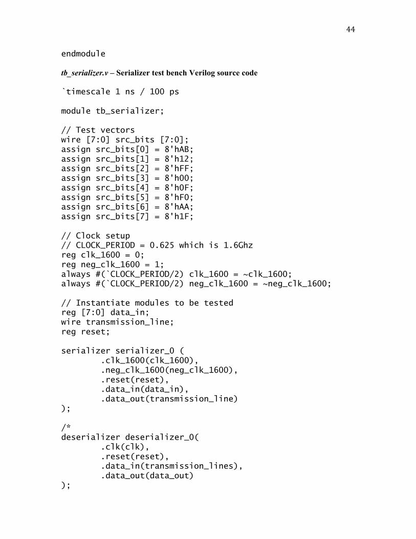
! 44!
endmodule
tb_serializer.v – Serializer test bench Verilog source code
`timescale 1 ns / 100 ps module tb_serializer; // Test vectors wire [7:0] src_bits [7:0]; assign src_bits[0] = 8'hAB; assign src_bits[1] = 8'h12; assign src_bits[2] = 8'hFF; assign src_bits[3] = 8'h00; assign src_bits[4] = 8'h0F; assign src_bits[5] = 8'hF0; assign src_bits[6] = 8'hAA; assign src_bits[7] = 8'h1F; // Clock setup // CLOCK_PERIOD = 0.625 which is 1.6Ghz reg clk_1600 = 0; reg neg_clk_1600 = 1; always #(`CLOCK_PERIOD/2) clk_1600 = ~clk_1600; always #(`CLOCK_PERIOD/2) neg_clk_1600 = ~neg_clk_1600; // Instantiate modules to be tested reg [7:0] data_in; wire transmission_line; reg reset; serializer serializer_0 ( .clk_1600(clk_1600), .neg_clk_1600(neg_clk_1600), .reset(reset), .data_in(data_in), .data_out(transmission_line) ); /* deserializer deserializer_0( .clk(clk), .reset(reset), .data_in(transmission_lines), .data_out(data_out) );

! 45!
*/ // Iterate over test vectors reg [7:0] test_index; reg [7:0] data_index; initial begin $vcdpluson; test_index = 0; assign data_in = src_bits[test_index]; // Strobe reset repeat(5) @(negedge clk_1600) reset <= 0; repeat(5) @(negedge clk_1600) reset <= 1; @(negedge clk_1600) reset <= 0;
// Test each vector and display results for(test_index = 0; test_index < 8; test_index = test_index + 1) begin for(data_index = 0; data_index < 8; data_index = data_index + 2) begin @(posedge clk_1600); if(transmission_line == src_bits[test_index][data_index]) $display("PASSED test %d, data bit %d", test_index, data_index); else $display("FAILED test %d, data bit %d: transmission_line = %d, src_bits[text_index][data_index] = %d",test_index, data_index, transmission_line, src_bits[test_index][data_index]); @(negedge clk_1600); if(transmission_line == src_bits[test_index][data_index+1]) $display("PASSED test %d, data bit %d", test_index, data_index+1); else $display("FAILED test %d, data bit %d: transmission_line = %d, src_bits[text_index][data_index] = %d",test_index, data_index+1, transmission_line, src_bits[test_index][data_index+1]); end end $vcdplusoff; $finish; end

! 46!
endmodule