NAVSPACECOM Space Surveillance Sensor System Digital ...
35
NRL/FR/I150--94-9715 NAVSPACECOM Space Surveillance I Sensor System Digital Signal Processing Receiver Volume 4-Hardware Interfaces CARL J. MoRRu STIC CAROLYN F. BRYANT 'm YL4CT9 Space Applications Branch D Space Systems Development Department P-6c 94-13227 April 6, 1994 Approved for public release; distribution unlimited. 94 5 02 097
Transcript of NAVSPACECOM Space Surveillance Sensor System Digital ...
NRL/FR/I150--94-9715
NAVSPACECOM Space SurveillanceI Sensor System Digital Signal
Processing Receiver
Volume 4-Hardware Interfaces
CARL J. MoRRu STICCAROLYN F. BRYANT 'm YL4CT9
Space Applications Branch DSpace Systems Development Department
P-6c 94-13227
April 6, 1994
Approved for public release; distribution unlimited.
94 5 02 097

REPORT DOCUMENTATION PAGE o Af0veI OMB NO. o0o,,-o?88
Public reporting burde for f. coliection of Information is estimated to oeoq I how per respone. incuding d time for reviewin insutuctions. e•chig existing date "mos,gatherqinge and mrnaln ; the dae needed. •nd compleat• and revWing th collection of iformaion. Sand comme•nt regarding iOft i eetwte or ary othe aspect of thiscolecton of inlormation. inluding eugeetioni for educing t"e burden, to Washington Heedquarters Services. Directorate for Information Operatic and Reports. 1216 JeffersonDavis Higiwey. Suite 1204. Arlington. VA 222024302. and to the Office of Menegernent and Budget. Peperwork Reduction Project 10704-0101). Weheglton. DC 20603.
1. AGENCY USE ONLY ILea•r lenk) 2. REPORT DATE 3. REPORT TYPE AND DATES COVERED
April 6, 1994 Final Oct. 1990- Sept. 19934. TITLE AND SUBTITLE 5. FUNDING NUMBERS
NAVSPACECOM Space Surveillance Sensor System Digital Signal Processing Receiver PE - 12427NVolume 4-Hardware Interfaces PU - X-0125
WU - DN780-065
6. AUTHOR(S)
Carl J. Morris and Carolyn F. Bryant
7. PERFORMING ORGANIZATION NAMEIS) AND ADDRESS(ES) e. PERFORMING ORGANIZATIONREPORT NUMBER
Naval Research LaboratoryWashington, DC 20375-5320 NRL/FR/8150-94-9715
9. SPONSORINGIMONITORING AGENCY NAME(S) AND ADDRESS(ES) 10. SPONSORING/MONITORINGAGENCY REPORT NUMBER
Naval Space CommandDahlgren, VA
11. SUPPLEMENTARY NOTES
12s. DISTRIBUTION/AVAILABILITY STATEMENT 12b. DISTRIBUTION CODE
Approved for public release; distribution unlimited.
13. ABSTRACT (Meximum 200 words)
This is a system description of the Naval Space Command (NAVSPACECOM) Space Surveillance Sensor System Digital SignalProcessing Receiver (DSPR). Formerly known as NAVSPASUR, the Space Surveillance system began as an advanced researchproject in June 1958, was commissioned as a operational Naval command in February 1961, and is operated by NAVSPACECOM'sSpace Surveillance Processing Center in Dahlgren, Virginia. The DSPR is a real-time radar data acquisition and analysis system.Its function is to detect, with no prior information, all space objects whose orbits cross the continental United States and to computetheir subsequent orbits. It provides vital satellite information in support of national defense mission objectives of space intelligence,saiellite attack warning, satellite intercept support, and space mission support. This system description was prepared as part of amodernization program that has replaced DSPR hardware for which parts are no longer available.
Volume 3 describes the operating system functions required by the applications software. Volume 4 describes the hardwareinterfaces between the major subsystems of the DSPR and identifies critical timing paths and interrupts between subsystems.Previously published, Volume 1 (NRL/FR/8154-93-9577) presents an overview of the hardware and software of the DSPR system,and Volume 2 (NRL/FR/8154-93-9578) discusses the function and capabilities of individual software and hardware components ofeach subsystem.
14. SUBJECT TERMS 15. NUMBER OF PAGES
Radar 35Satellite 16. PRICE CODEInterferometry
17. SECURITY CLASSIFICATION 18. SECURITY CLASSIFICATION 19. SECURITY CLASSIFICATION 20. LIMITATION OF ABSTRACTOF REPORT OF THIS PAGE OF ABSTRACT
UNCLASSIFIED UNCLASSIFIED UNCLASSIFIED UL
NSN "7540-01-280-5500 Standard Form 298 (Rev. 2-89)Prescribed by ANSI Std 239-18
298-102
CONTENTS
1. INTRODUCTION ................................................ I1.1 Purpose and Scope ........................................... 11.2 System Overview .............................................. 21.3 DSPR System Philosophy .. ....................................... 21.4 DSPR Subsystems .............................................. 3
2. HARDWARE INTERFACES ........................................... 42.1 Radio Frequency (RF) Subsystem Interfaces .............................. 42.2 System Monitor and Control Subsystem Interfaces ......................... 52.3 Utility Bus Control Subsystem Interfaces ............................... 132.4 Target Detection and Selection Subsystem Interfaces ....................... 212.5 Interferometer Subsystem Interfaces .................................. 222.6 Data Line Communications Subsystem Interfaces ......................... 272.7 Interprocessor Communications Subsystem Interfaces ...................... 272.8 Calibration and Diagnostics Subsystem Interfaces ......................... 27
3. CRITICAL TIMING PATHS .......................................... 273.1 Target Detection and Selection Subsystem ............................. 273.2 System Timing Subsystem ........................................ 283.3 Data Processing Subsystem .. ..................................... 283.4 Interferometer Data Collection Subsystem ............................. 28
4. HIGH-ALTITUDE SYSTEM ........................................... 284.1 RF Subsystem ................................................ 294.2 Target Detection and Selection Subsystem ............................. 294.3 Utility Bus Control Subsystem .. ................................... 29
5. ACKNOWLEDGMENTS ........................................... 30
ACRONYMS AND ABBREVIATIONS ...................................... 31
TABLES
Table 1 - Utility Bus I/O Card Connections for Jl and J3 .......................... 8Table 2 - Utility Bus I/O Card Connections for J2 and J4 .......................... 9Table 3 - Array Processor I/O Card Connections for J3 and BG31 ................... 15Table 4 - Utility Bus I/O Card Connections for BGI and J4 ....................... 16Table 5 - Digital Filter I/O Card Connector J3.................................. 25Table 6 - Digital Filter I/O Card Connector J4.................................. 26
iii
FIGURES
Fig. I - DSPR components diagram ...................................... 6Fig. 2 - Utility bus block diagram ....................................... 14
Fig. 3 - Data Distribution and Test Card connections ........................... 17Fig. 4 - High-altitude alert interconnections ................................. 29
Fig. 5 - High-altitude utility bus connections ................................. 30
Accession Yor 'i
I TIS R&DTIC TAB ]u•mooaZnced 0J.,tificatiO
By
Distributionflti,Ava'ILjiity o ,deS
a nd/or
Maet speo 181
iv
NAVSPACECOM SPACE SURVEILLANCE SENSOR SYSTEMDIGITAL SIGNAL PROCESSING RECEIVER
Volume 4-Hardware Interfaces
1. INTRODUCTION
This is Volume 4 of a four-volume system description of the Naval Space Command(NAVSPACECOM) Space Surveillance Sensor System Digital Signal Processing Receiver (DSPR)hardware and software. The hardware was developed by the Naval Research Laboratory (NRL) for theNAVSPACECOM Space Surveillance System (formerly NAVSPASUR). The software was designed byNRL and developed jointly by Digital Equipment Corporation (DEC) and NRL. The modernizedsoftware described in this volume was designed and developed by NRL.
The NAVSPACECOM Space Surveillance system began as an advanced research project in June1958. In October 1960, the project was transferred from the Advanced Research Projects Agency(ARPA) to the Navy, and was subsequently commissioned as an operational Naval command in February1961. Since then, it has been operated by the NAVSPACECOM Space Surveillance Processing Centerin Dahlgren, Virginia. The Processing Center is responsible to the Chief of Naval Operations for supportto the operating forces of the United States Navy, and is under the operational control of the U.S. SpaceCommand, Colorado Springs, Colorado, for those space object data collection functions that are part ofthe National Space Detection and Tracking System (SPADATS).
1.1 Purpose and Scope
This volume describes the hardware interfaces between the major subsystems of the DSPR andidentifies the critical timing paths and interrupts between different subsystems in terms of their currentfunctionality. Volume I presents a hardware and software overview of the DSPR system. Volume 2describes the function and capabilities of individual software and hardware components of the system.Volume 3 describes the operating system functions that are required by the applications software.
The documentation supports a project that has replaced DSPR hardware for which parts are nolonger available. Hardware replaced includes the DEC PDP-11/60 minicomputers that served as thecentral processors for the DSPR system, the Floating Point Systems Array Processors that performed fastFourier transforms on data from the alert antennas, and various interface hardware. New hardwareinstalled includes the VAX 4200 minicomputers, CSPI MAP 4000 array processors, and updated interfacehardware. All new hardware and associated software were required to interface with the rest of theexisting system. The new software was required to replicate all the functions of the existing software.
Manuscript approved January 31, 1994.
S. . . ... . .. . . - - -- -- • m m • nM mn uto n n nmm n u I I1
2 Morris and &yaw
The set of documents describes the DSPR system in terms of its current functionality withmodernized hardware and software. It will serve as a baseline description from which futurespecifications for upgrades to hardware and software may be drawn.
1.2 System Overview
The Digital Signal Processing Receiver is a real-time radar data acquisition and analysis system.The function of the NAVSPACECOM Space Surveillance system is to detect, with no prior information,all space objects whose orbits cross the continental United States and to compute their subsequent orbits.
The Space Surveillance system is a multistatic continuous-wave radar system operating as a largeradio interferometer, with nine stations located along a great-circle path across the southern United States.The inclination of the great circle is 33.570 with respect to the equator.
The system consists of three transmitters and six receivers. The stations are located as follows:
Transmitters: Jordan Lake Station, Wetumpka, AlabamaLake Kickapoo Station, Archer City, TexasGila River Station, Maricopa, Arizona
Receivers: Tattnall Station, Glennville, GeorgiaHawkinsville Station, Hawkinsville, Georgia (high altitude)Silver Lake Station, Hollandale, MississippiRed River Station, Lewisville, ArkansasElephant Butte Station, Truth or Consequences, New Mexico
(high altitude)San Diego Station, Chula Vista, California
Each transmitting station radiates a continuous wave of radio energy that combines with the othertransmitting stations' beams to form the Space Surveillance "fence." When an object, such as a satellite,enters the fence, a small fraction of the radio energy is reflected to one or more of the receiver sites.The receiving stations use large multiple-array interferometers to detect the reflected signal and tomeasure its angle of arrival. The transmitter and receiver arrays are cross-polarized to prevent thetransmitted energy from reaching the receivers without having been reflected from a space object. Eachreceiving station transmits phase and amplitude data, along with frequency identifiers, statistical measures,and time stamps to the Space Surveillance Processing Center via a dedicated telephone line, where localdirection angles for each object are computed.
The antenna data available at the receiver stations can be processed to produce three types of data:full-Doppler, half-Doppler, and quarter-Doppler. These three types are also referred to as low-altitude,mid-altitude, and high-altitude, respectively. The output of the full-Doppler data is far more importantthan either the half- or quarter-Doppler data. For this reason, production of the full-Doppler data by theDSPR system takes priority over half- and quarter-Doppler processing. The purpose, then, of each DSPRis to provide a continuous stream of full-Doppler data to the Space Surveillance Processing Center atDahlgren, Virginia.
1.3 DSPR System Philosophy
The DSPR system philosophy stems directly from the system purpose. This system is designedto run continuously, with any single component failure resulting in, at most, a very short (less than a
NAMSPACECOM Spawe Surveillawc DSPR 4 3
minute) interruption in full-Doppler data processing. For this reason, each DSPR actually consists of twosystems that duplicate each other. The primary system normally handles the full-Doppler data from theantennas. The secondary system normally handles the half- and quarter-Doppler data. If the primarysystem malfunctions and is no longer able to process data, the secondary system detects the failure anddeclares a "primary system failure." The secondary system then reinitializes itself to become a primarysystem. This reinitialization process occurs only in the secondary system. If, under normal conditions,the secondary system malfunctions, the primary system detects the failure, but does not attempt to processthe half- and quarter-Doppler data. This dual system philosophy is embedded in every aspect of theDSPR system.
1.4 DSPR Subsystems
For the purposes of this document, the DSPR is treated as consisting of the following subsystems.Their functions are briefly described below.
Radio Freuency converts the analog outputs from the antenna arrays to digital form forsubsequent processing.
System Monitor and Control initializes all other procedures, controls the system operation, andserves as the interface between the operators and the system.
Utility Bus Control directs and supervises activity on the utility bus and related hardwareelements that were designed and developed by NRL.
Target Detection and Selection performs the initial detection of targets that enter the SpaceSurveillance fence and compiles target lists that are used for target selection. The detectionprocedure runs in a CSPI MAP 4000 Array Processor; the selection procedure (TRGSEL) runsin the central controller, a DEC VAX 4000 Model 200 (VAX 4200).
Interferometer Data Collection takes the targets selected by the central controller and tunes thedigital filters to gather data. Accumulated data is provided to the VAX 4200 for formatting andtransmission to the Space Surveillance Processing Center.
Data Processing formats the data collected by the Interferometer Data Collection subsystem fortransmission to the Space Surveillance Processing Center.
Data Line Communications is responsible for interfacing the DSPR system to the communicationsline to the Space Surveillance Processing Center.
Interprocessor Communications provides communications between the central controller of theprimary system and that of the secondary system.
Operational Tests (also called OPTESTs) are on-line confidence tests used to exercise one ormore components of the DSPR system.
Calibration and Diagnostics allows the operator to check the status of various hardwarecomponents of the system. It also generates calibration constants, used to process interferometerdata.
The Operational Tests subsystem is not discussed in this document.
4 Morris and Bryan
2. HARDWARE INTERFACES
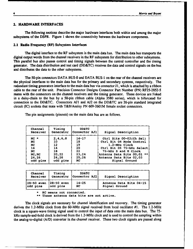
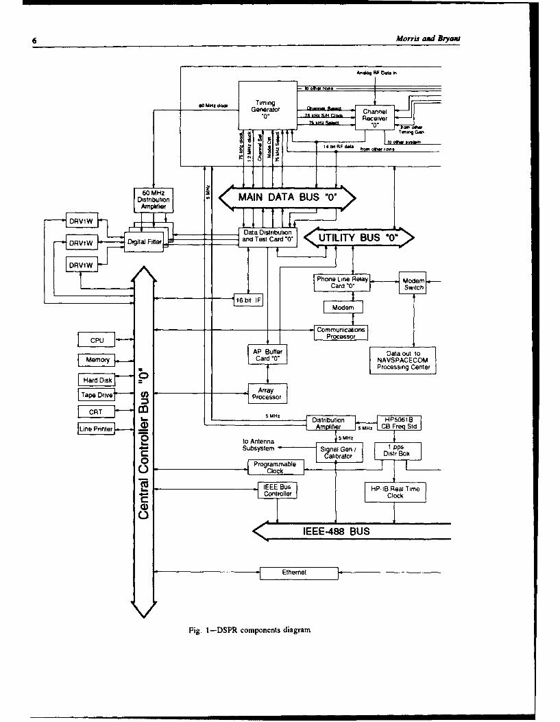
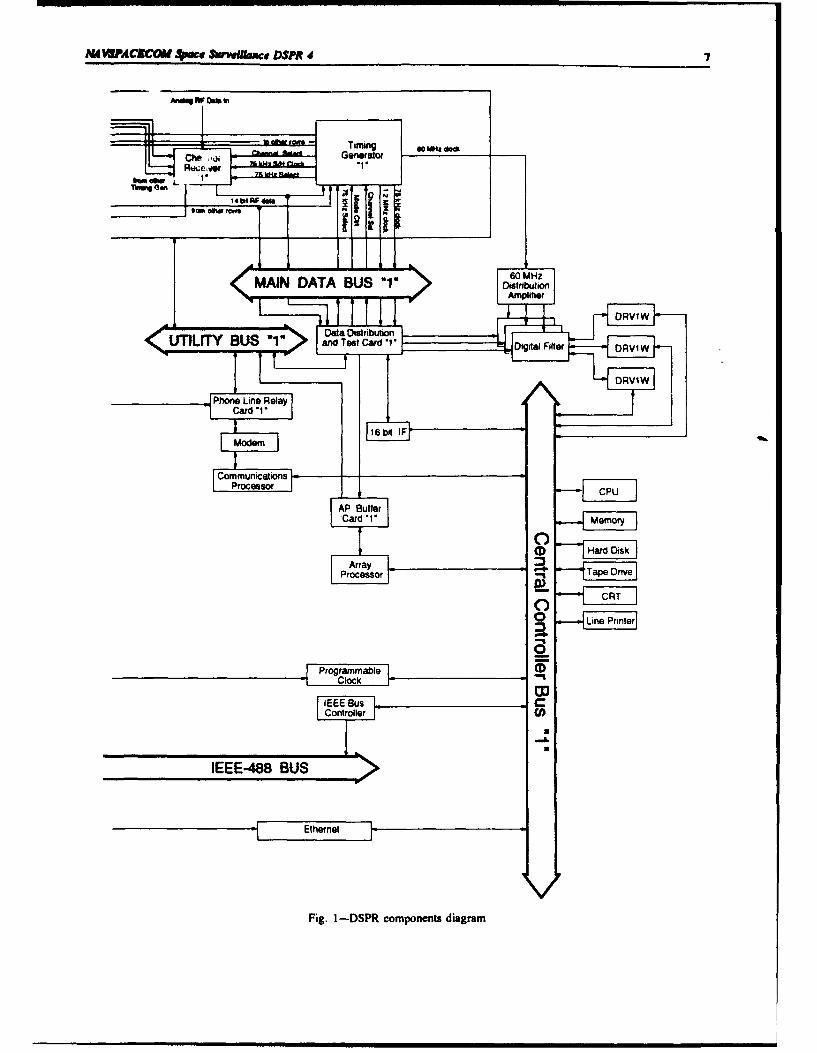
The following sections describe the major hardware interfaces both within and among the majorsubsystems of the DSPR. Figure 1 shows the connectivity between the hardware components.
2.1 Radio Frequency (RF) Subsystem Interfaces
The digital interface to the RF subsystem is the main data bus. The main data bus transports thedigital output words from the channel receivers in the RF subsystem for distribution to other subsystems.This parallel bus also passes control and timing signals between the central controller and the timinggenerator. The data distribution and test card (DD&TC) receives the data and control signals on the busand distributes the data to the other subsystems.
The 50-pin connectors DATA BUS-0 and DATA BUS-I on the rear of the channel receivers arethe physical interfaces to the main data bus for the primary and secondary systems, respectively. Theredundant timing generators interface to the main data bus via connector J 1, which is attached by a ribboncable to the rear of the unit. Precision Connector Designs Connector Part Number (PN) RF25-2852-5mates with the connectors on the channel receivers and the timing generator. These devices are linkedin a daisy-chain to the bus by a 50-pin ribbon cable (Alpha 3580 series), which is bifurcated forconnection to the DD&TC. Connectors AJ l and AJ2 on the DD&TC are 26-pin standard integratedcircuit (IC) sockets that mate with T&B/Ansley PN 609-2601M female socket connectors.
The pin assignments (pinouts) on the main data bus are as follows.
Channel Timing DD&TCReceiver Generator Connector AJi Signal Description
NC * 2,4,6,8 14-17 Ctrl Bits 00-03(Ch Sel)NC 10 18 Ctrl Bit 04 Mode ControlNC 12 19 1.2-MHz Clock14 14 20 Ctrl Bit 05 75-kHz SelectNC 18 22 75-kHz S and H ClockNC,NC 20,22 23,24 Antenna Data Bits 00,01 **24,26 24,26 25,26 Antenna Data Bits 02,03odd pins odd pins NC Signal Ground
Channel Timing DD&TCReceiver Generator Connector AJ2 Signal Description
28-50 even 28-50 even 14-25 Antenna Data Bits 04-15odd pins odd pins NC Signal Ground
• NC means not connected.** These antenna data bits are not active.
The clock signals are necessary for channel identification and recovery. The timing generatorderives the 1.2-MHz clock from the 60-MHz signal received from local oscillator #1. The 1.2-MHzclock is a square-wave timing signal used to control the input of data onto the main data bus. The 75-kHz sample-and-hold clock is derived from the 1.2-MHz clock and is used to control the sampling withinthe analog-to-digital (A/D) converter in the channel receiver. These two clock signals are passed along
MAVSPACECOM Space Surveillance DSPR 4 5
with the 14 antenna bits comprising the digitized RF data to the data distribution and test card fordistribution to the Interferometer subsystem and the Target Detection and Selection subsystem.
The control signals originate from the central controller and are passed to the DD&TC via theutility bus. The channel select bits identify which antenna channel to use to load data in the test mode.The (test) mode control bit determines the mode by which the timing generator places data on the bus.The "Auto" mode places data from all the channels on the bus in the normal fashion, whereas in the"Load" mode, data from the antenna identified in control bits 0-3 will be placed on all the channels onthe bus. The 75-kHz select signal determines which of the 75-kHz clocks from the two systems is to beenabled. This signal is passed to the channel receivers.
2.2 System Monitor and Control Subsystem Interfaces
The primary hardware component in the System Monitor and Control Subsystem is the DigitalEquipment Corporation VAX 4000 Model 200 (VAX 4200) minicomputer. The VAX 4200 is the centralcontroller for the DSPR and communicates with external devices via the Qbus. The communications andprocessing cards that interface the Qbus to external devices have the standard backplane Qbus interfacewith the VAX 4200. The cards' interfaces with the external devices are described in the followingsubsections.
2.2.1 Utility Bus Control Subsystem
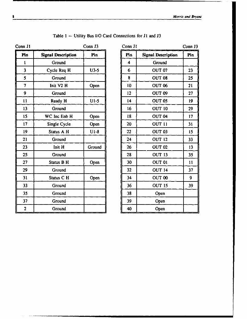
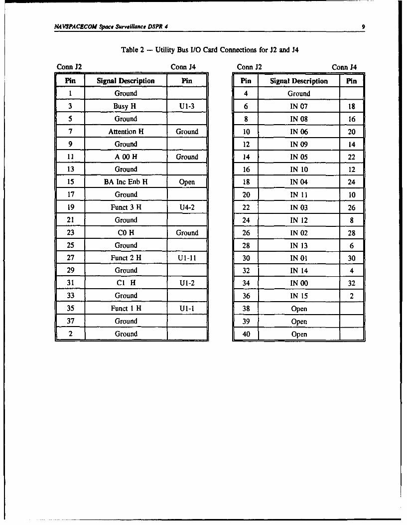
The DRVIW input/output (I/O) 16-bit parallel interface, in conjunction with a utility businput/output (UBIO) interface card, provides the interface between the Qbus and the utility bus (UB).The UBIO card is identical to the digital filter input/output (DFIO) card except for the position of jumperJ1. The DRVlW1 has two 37-pin D connectors (JI and J2) on its front panel. The DRVlW is connectedto the UBIO by a 40-conductor ribbon cable. On the DRVIW end is a 3M 37-pin D to ribbon connectorPN 3485-2400, and on the UBIO end (11 and J2) are female Bergcon-type connectors. Because the utilitybus cards were originally designed to interface with a Unibus DRI 1-K, the UBIO is required to generatecontrol signals for the DRV1W and the utility bus cards. The UBIO is connected to the utility bus bytwo 40-conductor ribbon cables (J3 and J4) with female Bergcon connectors on the UBIO end and a low-profile, 40-contact DIP plug such as T&B/Ansley PN 609-M407H, which plugs into connector areas BG land BG31 on the data distribution and test card. The pin assignments for J1-J3 and J2-44 of the UBIOare given in 'fables 1 and 2. The high byte of the 16-bit data word is defined as the UB card address.The low byte contains the data pertaining to the addressed device.
1 DRVI1-WA General Purpose DMA Interface, DEC User's Guide EK-DRVWA-UG-002, 1986.
Morrij axd Bryant
AAW" RF 0ý" on
to 91by rows
00 MHz d0a TimingGenerator Channel
Receiver.0. am 010WTm" Gen
sysbmI.-14 tot.RF come hom OWW, S
I! 7j.'
X460 MHz aDistribution MAIN DATA BUS "0'
Amplifier
DRVlW Data Distrib tion
DRVIW Do dal Fitter and Test Ca "0' UTILITY BUS 000
DRVIW
Phone Line Relay ModemCard '0* Switch
Modem
CommunicationsCPU Processor
AP Buffer Data outmemory Card V NAVSPACECOOM
X Processing Center
Hard Disk
Pr Arr or
CRT S MHz
:ETitrobuhon HP6061B)lit _older sm z CB Freq StdLine Printer =
0 to Antenna 5 MHzSubsystem Signal Gen i I pps
::; Calibrator Distr Box
0 Programýmable "zClock
IEEE Bus HP-IB Real TimController Clock
EEE-488 BUS
Ethernet
Fig. I-DSPR componcrits diagram
44 VSPA CZCOM $pwe S~rve~tmce DSPWR4 7
60Mz
Ph Line Relnay
Fag. 1 -DP opnet iga
Morris and Bryant
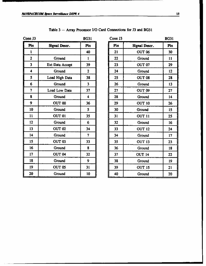
Table I - Utility Bus I/O Card Connections for JI and J3
Conn Jl Conn J3 Conn J l Conn J3
Pin Signal Description Pin Pin Signal Description Pin
1 Ground 4 Ground
3 Cycle Req H U3-5 6 OUT 07 23
5 Ground 8 OUT 08 25
7 lnit V2 H Open 10 OUT 06 21
9 Ground 12 OUT 09 27
11 Ready H U1-5 14 OUT 05 19
13 Ground 16 OUT 10 29
15 WC Inc Enb H Open 18 OUT 04 17
17 Single Cycle Open 20 OUT 11 31
19 Status A H UI-8 22 OUT 03 15
21 Ground 24 OUT 12 33
23 Init H Ground 26 OUT 02 13
25 Ground 28 OUT 13 35
27 Status B H Open 30 OUT 01 11
29 Ground 32 OUT 14 37
31 Status C H Open 34 OUT 00 9
33 Ground 36 OUT 15 39
35 Ground 38 Open
37 Ground 39 Open
2 Ground 40 Open
NAVSPACECOM Space Surveillance DSPR 4 9
Table 2 - Utility Bus I/O Card Connections for J2 and J4
Conn J2 Conn J4 Conn J2 Conn J4
Pin Signal Description Pin Pin Signal Description Pin
1 Ground 4 Ground
3 Busy H U1-3 6 IN 07 18
5 Ground 8 IN 08 16
7 Attention H Ground 10 IN 06 20
9 Ground 12 IN 09 14
11 A 00 H Ground 14 IN 05 22
13 Ground 16 IN 10 12
15 BA Inc Enb H Open 18 IN 04 24
17 Ground 20 IN 11 10
19 Funct 3 H U4-2 22 IN 03 26
21 Ground 24 IN 12 8
23 CO H Ground 26 IN 02 28
25 Ground 28 IN 13 6
27 Funct 2 H Ul-11 30 IN 01 30
29 Ground 32 IN 14 4
31 C1 H U1-2 34 IN 00 32
33 Ground 36 IN 15 2
35 Funct 1 H UI-1 38 Open
37 Ground 39 Open
2 Ground 40 Open

10 Morris and Bryant
The following paragraphs describe the operation of utility bus and DRVIW control signals.
Utility Bus Control Signals: The input control bit "Internal Data Accept" indicates that the centralcontroller has accepted the data on the utility bus. The output bit "External Data Ready" indicates thatthe utility bus has data available for the central controller. The command data are directed to the utilitybus device addressed in the command address bits. The two output control bits, "Internal High DataReady" and "Internal Low Data Ready," indicate that the DRVIW has data available for the utility bus."Internal High Data Ready" indicates that the eight most significant bits (high byte) of DRV IW data areon the utility bus. "Internal Low Data Ready" indicates that the eight least significant bits (low byte) ofDRVIW data ar- on the utility bus. The input bit "External Data Accept" indicates that the addresseddevice has accepted the data on the utility bus.
DRVIW Control Signals: The DRVIW control signals are "Ready," "Busy," "CO and Cl," and"Cycle Request." Transfers are controlled by the user device. There are three function bits which canbe set by the DRV1W and three status bits which can be set by the user and read by the DRVIW. Thedirection of the transfer is determined by CI with CO held high. C1 is set high for a transfer into theDRVIW from the UB; it is set low for a write to the UB. Function bit F1 is used to control the valueof Cl.
Theory of Operation: For a transfer to the UB, function bits 1, 2, and 3 are set. Function bit 1is returned through an inverter as "CO" and also enables "Load High Data." Function bit 2 enables the"Ready" signal as the input to an SN74123 dual monostable multivibrator, or single shot. Function bit 3enables "Load Low Data." After the function bits are set, the DRVIW sets "Ready" low to indicate itis ready for a transfer. Ready is passed to an SN74123 dual single shot. The output is sent to theDRVIW as "Cycle Request." The DRVIW sends "Busy," which is passed to the UB as "Load LowData" and "Load High Data." Each card on the UB compares the address byte to its own address, whichis set by switches. If they match, the card loads the data byte into its data register. It also passes theload signal back on the bus as "External Data Accepted." The "Busy" signal also enables the othersingle shot, whose output is passed to the UB as "Internal Data Accepted" and to the A input of the firstsingle shot to start another "Cycle Request" pulse. When the transfer is complete, "Ready" is assertedhigh.
For a transfer from a card on the UB, first a write cycle is performed with only function bits F1and F2 set. The "Load High Data" signal generated from Fl and the output of the second single shotforces the addressed card to place its data and address on the bus. Then a read is performed with allfunction bits clear. The DRVIW stores the data on the bus in the VAX 4200 memory.
2.2.2 Target Detection and Selection Subsystem
The CSPI MAP 4000 array processor consists of four boards: a host interface (HINT) board, aCPU board, a main memory board, and a direct input/output (DIO) interface board. The DIO is modeledon the DEC DRVlW 16-bit parallel interface card. The MAP 4000 plugs into the VAX 4200 chassis.The Qbus HINT board provides the translation and handshaking signals needed between the VAX 4200and the host interface in the array processor. The MAP 4000 is totally software controlled by the centralcontroller via the host interface. A custom array processor input/output (APIO) card is used to selectalert antenna data from the main data bus and pass it to the DIO for entry into the MAP 4000.
NA VSPACECOM Space Surveiliance DSPR 4 11
2.2.3 Interferometer Subsystem
The Interferometer subsystem consists of three digital filters (DFs). A DRV1W/DFIOcombination is responsible for data transfer and control between each DF and the central controller. Thefollowing paragraphs describe the operation of digital filter and DRVIW control signals.
Digital Filter Control Signals: The input control bit "Internal Data Accept" indicates that thecentral controller has accepted data from the DF. The output bit "External Data Ready" indicates thatthe DF has data available for the central controller. The command data are directed to the DF registeraddressed in the command address bits. The output control bit "Internal High Data Ready" indicates thatthe DRV1W has data available for the DF. This bit is returned by the DF as input bit "External DataAccept" to indicate that the DF has accepted the data.
DRV1W Control Sienals: The DRVIW control signals are "Ready," "Busy," "CO and CI," and"Cycle Request." Transfers are controlled by the user device. There are three function bits which canbe set by the DRVIW and three status bits which can be set by the user and read by the DRVIW. Thedirection of the transfer is determined by C1 with CO held high. CI is set high for a transfer into theDRV1W from the DF and low for a write to the DF. Function bit FI is used to control the value of CI.
Theory of Operation: For a transfer to the DF, function bits I and 2 are set. Function bit 1 isreturned through an inverter as "CO" and also enables "Load High Data." Function bit 2 enables the"Ready" signal as the input to a single shot. After the function bits are set, the DRVIW sets "Ready"low to indicate it is ready for a transfer. "Ready" is passed to an SN74123 dual single shot. The outputis sent to the DRVIW as "Cycle Request." The DRVlW sends "Busy," which is passed to the DF as"Load High Data." The DF loads the data into the register indicated by the address bits of the inputword and returns "High Data Ready" as "External Data Accepted." The "Busy" signal also enables theother single shot, whose output is passed to the DF as "Internal Data Accepted." "External DataAccepted" is passed to the A input of the first single shot to start another "Cycle Request" pulse. Whenthe transfer is complete, "Ready" is asserted high, which inhibits "Cycle Request."
For a transfer from the DF, a read is queued with the function bits cleared. Function bit 1 isinverted and is returned as "CO" to indicate a read. Function bit 2 being clear enables "External DataReady" as the trigger for the first single shot. After the DF has completed a discrete Fourier transform(DFT), it places its first data word on the DRVlW input lines and sets "External Data Ready," whichinitiates a "Cycle Request." "Busy" is set by the DRV1W and passed to the DF as "Internal DataAccepted." The DF places the next data word on the input bus on the trailing edge of "Busy" andinitiates an "External Data Accepted" pulse. This signal enables the first single shot, and another "CycleRequest" is generated. After all the data from the DFT has been transmitted (56 16-bit words), "DataReady" is cleared and the system waits for another DFT to be completed.
2.2.4 Data Line Communications Subsystem
The Codex V.3225 modem interfaces to the central controller via the DSVI I synchronousinterface using a standard RS-232C interface. The DSVI 1 has two independent channels, of which theDSPR system uses channel 0. Connector JO on the DSV 1I is a 50-pin male D connector. An 8-foot 50-pin to 25-pin cable adapts the output to an RS-232C 25-pin male connection which runs to J4 of thejunction panel. A 15-foot 25-pin male-to-female cable connects the junction panel J4 to the modem.
12 Morris and Bryant
The following signals are active:
Transmit Data (TD) Receive Data (RD)Transmit Clock (TC)Receive Clock (RC)Data Terminal Ready (DTR) DCE Receiver Ready (DSR)Request to Send (RTS) Clear to Send (CTS)Carrier Detect (RLSD)Ring Indicator (RI)External Transmit Clock (ETC)
2.2.5 Interprocessor Communications Subsystem
The Interprocessor Communications subsystem (ICC) uses the Ethernet controller imbedded onthe CPU card of the VAX 4200. The VAX 4200 has both a thickwire and thinwire connection. TheDSPR system uses only the thinwire connection. A coaxial cable with male BNC connectors runs fromthe thinwire connection on the CPU front panel to J7 of the junction panel, which has a BNC feed-through connector. A 30-foot BNC male-to-male cable connects J7 of the two junction panels.
2.2.6 Calibration and Diagnostics Subsystem
The Qbus interface to the IEEE-488 bus is the IEQI 1 bus controller. The controller has twoindependent channels, of which only channel I is used by the DSPR system. Connector J 1 on the IEQ 1Iis a standard IEEE 24-pin connector.
2.2.7 Operator's Console
The operator's console consists of a VT240 video terminal and a LA120 line printer for eachsystem. The LA 120 is used as the VAX 4200 console and is connected to the console jack on the VAX4200 CPU front panel, which is a DEC-423 modular jack. An 8-foot cable with a DEC-423 MMJconnector on one end and a 9-pin D connector on the other connects the console to the junction panel.The VT420 is connected to line 0 of a DZQl1 four-line RS-232C communications card. The DZQI1has four 9-pin D connectors (one for each line) on its front panel. An 8-foot cable with 9-pin male andfemale connectors runs from the DZQI 1 to the junction panel. Both the LA 120 and VT240 run at 9600baud.
2.2.8 System Timing
The 1-pulse-per-second (pps) distribution box interfaces to the central controller via the KWV 1Iprogrammable real-time clock. The KWV 11 clock is used to obtain precise time for time stamping theobserved data. The I-pps signal is used to reset the counter in the clock. A coaxial cable with BNCconnectors runs from the distribution box to the Schmitt trigger 2 input of a UDIP-KW front panel, whichis located in the rear of the VAX 4200 rack. A cable with 25-pin D connectors runs from the UDIP-KWto the KWV 11 front panel.
The KWVI 1 interrupts the central controller to update the system clock based on the l-pps fromthe cesium time standard. Upon receiving the interrupt, the connect-to-interrupt code updates the systemtime.
MWSPACECOM Spae SwwiUawe DSPR 4 13
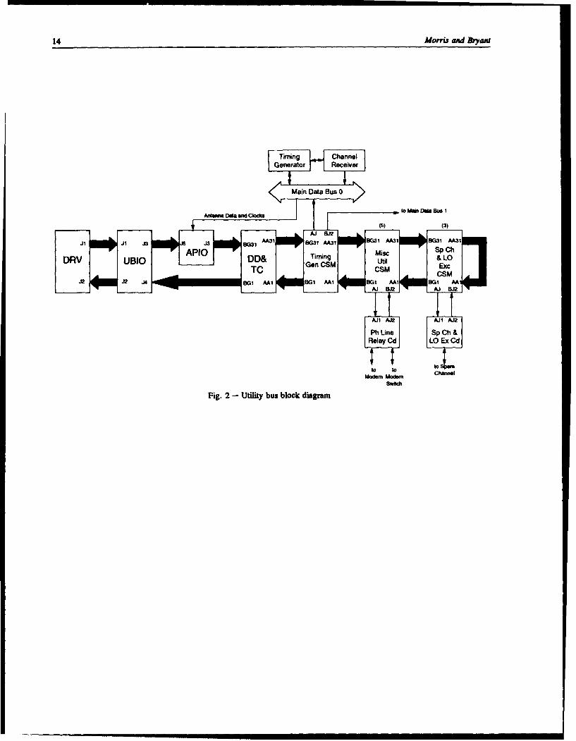
2.3 Utility Bus Control Subsystem Interfaces
The utility bus is used to initialize the custom hardware in the DSPR system and to detect changesin the hardware during system operation. As shown in Fig. 2, the hardware devices on the bus are linkedin a daisy-chain, and each has a specific address. The bus is 20 bits wide in each direction, consistingof eight bits of data, eight bits of addressing, and control signals.
The utility bus word is 16 bits long. The eight most significant bits (high byte) contain theaddress of the device (card). The eight least significant bits (low byte) contain the command or statusdata relating to the device. Data from the central controller to the utility bus consists of commands toenable/disable or change hardware features of the addressed device. Data to the central controller fromthe utility bus describe changes in hardware settings of the device associated with the address.
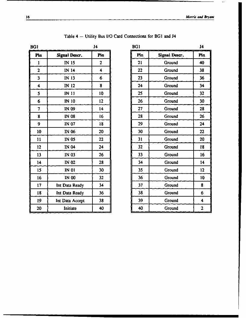
The utility cards connect to the VAX 4200 through the fourth DRV the Qbus and itsassociated UBIO card. The connectors on the UBIO are associated in pairs. J I contain the outputlines that handle commands to the UB cards, and J2 and J4 contain the input ..ies to the DRVIW.Control signals for the DRVIW and the UB are also on these connectors. Table 1 shows the UBIOconnections for J I and J3. Table 2 shows the connections for J2 and K4. J3 on the UBIO is connectedby a 40-conductor ribbon cable to Bergcon connector J6 on the APIO card. The signal is passed throughto the 40-pin Bergcon connector J3. A 40-pin ribbon cable connects J3 on the APIO card to area BG31on the DD&TC. A low-profile, 40-contact DIP plug T&B/Ansley PN 609-M407H is used to plug intoconnector area BG31 on the DD&TC. Table 3 gives the pinouts of this cable. The cards are daisy-chained on the utility bus and the bus is looped back to the input to the DRVIW. The APIO is not onthe input chain because it cannot return data to the VAX 4200. Table 4 gives the pinouts for the cablefrom area BG1 on the DD&TC to connector J4 on the UBIO card.
The signal descriptions for the command status module (CSM) connections are given in Section2.2.1.
2.3.1 System Monitor and Control Subsystem
The DRVIW is connected to the utility bus via the data distribution and test card. Thisconnection is shown in Fig. 2 and described in Section 2.2.1.
2.3.2 Data Distribution and Test Card
The DD&TC is the interface between the RF subsystem, the Target Detection and Selectionsubsystem, and the Interferometer subsystem. The DD&TC distributes data under control of the centralcontroller. Figure 3 shows the connector interfaces to the various subsystems.
Incorporated into this card are the CSM functions and connections to the bus with pin assignmentsas detailed in the previous section.
14 Morris aind Bryant
Tihnine Channe
Generato Reeie
Mainda DataBus
Fig.~~I 2-i Utalia bus blI iga
N.VSPACECOM 4,,pw Sun'e•awc# DSPR 4 15
Table 3 - Array Processor I/O Card Connections for B3 and BG31
Conn J3 BG31 Conn J3 BG31
Pin Signal Descr. Pin Pin Signal Descr. Pin
1 40 21 OUT 06 30
2 Ground 1 22 Ground 11
3 Ext Data Accept 39 23 OUT 07 29
4 Ground 2 24 Ground 12
5 Load High Data 38 25 OUT 08 28
6 Ground 3 26 Ground 13
7 Load Low Data 37 27 OUT 09 27
8 Ground 4 28 Ground 14
9 OUT 00 36 29 OUT 10 26
10 Ground 5 30 Ground 15
11 OUT 01 35 31 OUT 11 25
12 Ground 6 32 Ground 16
13 OUT 02 34 33 OUT 12 24
14 Ground 7 34 Ground 17
15 OUT 03 33 35 OUT 13 23
16 Ground 8 36 Ground 18
17 OUT 04 32 37 OUT 14 22
18 Ground 9 38 Ground 19
19 OUT 05 31 39 OUT 15 21
20 Ground 10 40 Ground 20
16 Morris and Bryan
Table 4 - Utility Bus I/O Card Connections for BGI and J4
BGI J4 BG1 J4
Pin Signal Descr. Pin Pin Signal Descr. Pin
1 IN 15 2 21 Ground 40
2 IN 14 4 22 Ground 38
3 IN 13 6 23 Ground 36
4 IN 12 8 24 Ground 34
5 IN 11 10 25 Ground 32
6 IN 10 12 26 Ground 30
7 IN 09 14 27 Ground 28
8 IN 08 16 28 Ground 26
9 IN 07 18 29 Ground 24
10 IN 06 20 30 Ground 22
11 IN 05 22 31 Ground 20
12 IN 04 24 32 Ground 18
13 IN 03 26 33 Ground 16
14 IN 02 28 34 Ground 14
15 IN 01 30 35 Ground 12
16 IN 00 32 36 Ground 10
17 Int Data Ready 34 37 Ground 8
18 Int Data Ready 36 38 Ground 6
19 Int Data Accept 38 39 Ground 4
20 Initiate 40 40 Ground 2

N4VSPACZCON 4pwe Sarovewe DSPR 4 17
BiAl B2 Antenna Data and ClocksMain Data Bus Al to APIO
In/Out A2
Cl Antenna Data and ClocksData C2 to Digital Filter Card 1-2Distribution
and D1 Antenna Data and ClocksCard to Digital Filter Card 2-2
El
E2 • Antenna Data and Clocksto Digital Filter Card 3-2
F1 Antenna Data and Clocks
F2 to APIO (High-Altitude)From APIO -- •AA1
Utility Bus AA31 Utility Bus out to Misc CSM
to UBIO BG31 BG1 Utility Bus from Misc CSM
Fig. 3 - Data Distribution and Test Card connections
is Moms and &yawu
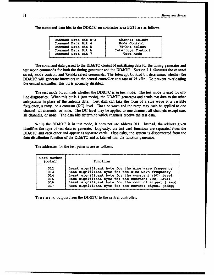
The command data bits to the DD&TC on connector area BG31 are as follows.
Command Data Bit 0-3 Channel SelectCommand Data Bit 4 Mode ControlCommand Data Bit 5 75-kHz SelectCommand Data Bit 6 Interrupt ControlCommand Data Bit 7 Test Mode
The command data passed to the DD&TC consist of initializing data for the timing generator andtest mode commands for both the timing generator and the DD&TC. Section 2.1 discusses the channelselect, mode control, and 75-kHz select commands. The Interrupt Control bit determines whether theDD&TC will generate interrupts to the central controller at a rate of 75 kHz. To prevent overloadingthe central controller, this bit is normally disabled.
The test mode bit controls whether the DD&TC is in test mode. The test mode is used for off-line diagnostics. When this bit is 1 (test mode), the DD&TC generates and sends test data to the othersubsystems in place of the antenna data. Test data can take the form of a sine wave at a variablefrequency, a ramp, or a constant (DC) level. The sine wave and the ramp may each be applied to onechannel, all channels, or none. The DC level may be applied to one channel, all channels except one,all channels, or none. The data bits determine which channels receive the test data.
While the DD&TC is in test mode, it does not use address 011. Instead, the address givenidentifies the type of test data to generate. Logically, the test card functions are separated from theDD&TC and each other and appear as separate cards. Physically, the system is disconnected from thedata distribution function of the DD&TC and is latched into the function generator.
The addresses for the test patterns are as follows.
Card Number(octal) Function
012 Least significant byte for the sine wave frequency013 Most significant byte for the sine wave frequency014 Least significant byte for the constant (DC) level015 Most significant byte for the constant (DC) level016 Least significant byte for the control signal (ramp)017 Most significant byte for the control signal (ramp)
There are no outputs from the DD&TC to the central controller.
NAVSPACECOM Sp"c Surve•anci DSPR 4 19
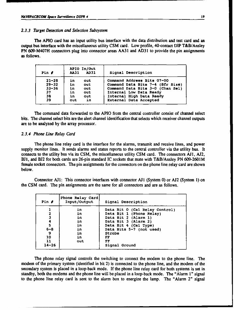
2.3.3 Target Detection and Selection Subsystem
The APIO card has an input utility bus interface with the data distribution and test card and anoutput bus interface with the miscellaneous utility CSM card. Low profile, 40-contact DIP T&B/AnsleyPN 609-M407H connectors plug into connector areas AA31 and AD31 to provide the pin assignmentsas follows.
APIO In/OutPin I AA31 AD31 Signal Description
21-28 in out Command Address Bits 07-0029-32 in out Command Data Bits 7-4 (Bfr Size)33-36 in out Command Data Bits 3-0 (Chan Sel)37 in out Internal Low Data Ready38 in out Internal High Data Ready39 out in External Data Accepted
The command data forwarded to the APIO from the central controller consist of channel selectbits. The channel select bits are the alert channel identification that selects which receiver channel outputsare to be analyzed by the array processor.
2.3.4 Phone Line Relay Card
The phone line relay card is the interface for the alarms, transmit and receive lines, and powersupply monitor lines. It sends alarms and status reports to the central controller via the utility bus. Itconnects to the utility bus via its CSM, the miscellaneous utility CSM card. The connectors AJI, AJ2,BJ1, and BJ2 for both cards are 26-pin standard IC sockets that mate with T&B/Ansley PN 609-2601Mfemale socket connectors. The pin assignments for the connectors on the phone line relay card are shownbelow.
Connector Al 1: This connector interfaces with connector All (System 0) or AJ2 (System 1) onthe CSM card. The pin assignments are the same for all connectors and are as follows.
Phone Relay CardPin I Input/Output Signal Description
1 in Data Bit 0 (Cal Relay Control)2 in Data Bit 1 (Phone Relay)3 in Data Bit 2 (Alarm 1)4 in Data Bit 3 (Alarm 2)5 in Data Bit 4 (Cal Type)
6-8 in Data Bits 5-7 (not used)9 in Strobe
10 in FF11 out FF
14-26 Signal Ground
The phone relay signal controls the switching to connect the modem to the phone line. Themodem of the primary system (identified in bit 2) is connected to the phone line, and the modem of thesecondary system is placed in a loop-back mode. If the phone line relay card for both systems is set instandby, both the modems and the phone line will be placed in a loop-back mode. The "Alarm 1" signalto the phone line relay card is sent to the alarm box to energize the lamp. The "Alarm 2" signal
20 Morrs and Bryant
energizes the buzzer that is connected to the alarm box. "Cal Relay Control" and "Cal Type" were twosignals associated with the calibrator in the production (old) receiver system. "Cal Relay" controlled theswitching between the production calibrator and the modernization (current) calibrator. "Cal Type"indicated whether the calibration signal was at the designated reference threshold. These two signals areobsolete since the production calibrator is no longer in use and the current calibrator is controlled by theIEEE-488 bus. This signal information is given here for clarification.
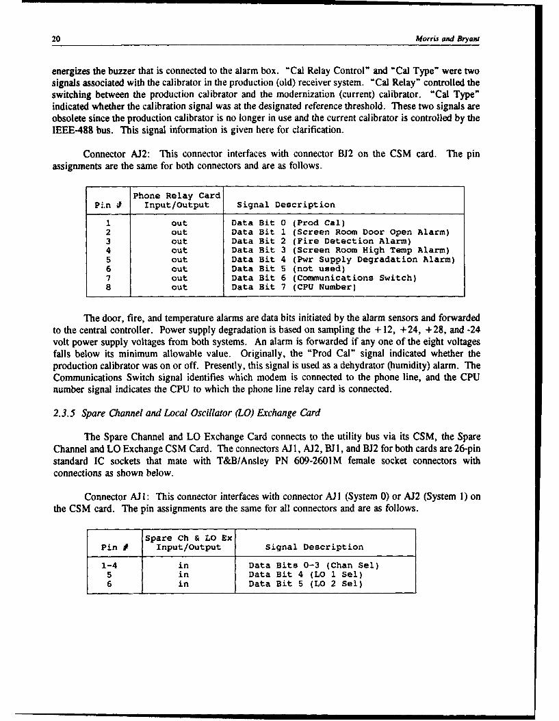
Connector AJ2: This connector interfaces with connector BJ2 on the CSM card. The pinassignments are the same for both connectors and are as follows.
Phone Relay CardPLn i# Input/Output Signal Description
1 out Data Bit 0 (Prod Cal)2 out Data Bit 1 (Screen Room Door Open Alarm)3 out Data Bit 2 (Fire Detection Alarm)4 out Data Bit 3 (Screen Room High Temp Alarm)5 out Data Bit 4 (Pwr Supply Degradation Alarm)6 out Data Bit 5 (not used)7 out Data Bit 6 (Communications Switch)8 out Data Bit 7 (CPU Number)
The door, fire, and temperature alarms are data bits initiated by the alarm sensors and forwardedto the central controller. Power supply degradation is based on sampling the + 12, +24, +28, and -24volt power supply voltages from both systems. An alarm is forwarded if any one of the eight voltagesfalls below its minimum allowable value. Originally, the "Prod Cal" signal indicated whether theproduction calibrator was on or off. Presently, this signal is used as a dehydrator (humidity) alarm. TheCommunications Switch signal identifies which modem is connected to the phone line, and the CPUnumber signal indicates the CPU to which the phone line relay card is connected.
2.3.5 Spare Channel and Local Oscillator (LO) Exchange Card
The Spare Channel and LO Exchange Card connects to the utility bus via its CSM, the SpareChannel and LO Exchange CSM Card. The connectors AJ 1, AJ2, BJ 1, and BJ2 for both cards are 26-pinstandard IC sockets that mate with T&B/Ansley PN 609-2601M female socket connectors withconnections as shown below.
Connector AJ 1: This connector interfaces with connector A] l (System 0) or AJ2 (System 1) onthe CSM card. The pin assignments are the same for all connectors and are as follows.
Spare Ch & LO ExPin # Input/Output Signal Description
1-4 in Data Bits 0-3 (Chan Sel)5 in Data Bit 4 (LO 1 Sel)6 in Data Bit 5 (LO 2 Sel)

NAVSPACECOM Sae Swvrwgw-e DSPR 4 21
Connector AJ2: This connector interfaces with connector BJ2 on the CSM card. The pinassignments are the same for both cards and are as follows.
Spare Ch & LO ExPin I Input/Output Signal Description
1 out Data Bit 0 (LO 1 '00 Status)2 out Data Bit 1 (LO 1 "1" Status)3 out Data Bit 2 (LO 1 Sol)4 out Data Bit 3 (LO 2 '00 Status)5 out Data Bit 4 (LO 2 "1' Status)6 out Data Bit 5 (LO 2 S.l)
The channel select bits form a four-bit data word that indicates which antenna channel the sparechannel switch shall select for the spare channel receiver. The input "LO Select" bits control whetherthe "0" or "1" oscillator circuit will be used for each local oscillator. The output "LO Status" bitsprovide the status of the local oscillator circuits. The output "LO Select" indicates the decision made bythe spare channel and LO exchange card based on the "LO Select" command from the central controllerand the status of the circuit.
2.4 Target Detection and Selection Subsystem Interfaces
The primary hardware components of the Target Detection and Selection subsystem are the CSPIMAP 4000 array processor and the APIO interface card. The System Monitor and Control interface isdescribed in Section 2.2.2 and the Utility Bus Control interface is described in Section 2.3.3.
2.4.1 Data Distribution and Test Card
The APIO card provides two interfaces between the subsystem and the DD&TC. The utility businterface is described in Section 2.3.3. The data interface to the APIO consists of alert channel data fromthe continuous stream of antenna data passing through the DD&TC. The APIO extracts this data andtransfers it to the MAP 4000 in 16-bit words. The connectors on the DD&TC are 26-pin standard ICsockets which mate with T&B/Ansley PN 609-2601M female socket connectors. The connectors on theAPIO card are 26-pin Bergcon-type connectors. The APIO card is connected to the MAP DIO boardthrough two 40-pin ribbon connectors with Bergcon-type connectors. By using the 75-kHz and 1.2-MHzclocks, the APIO determines when the data from the particular RF channel, input through the utility bus,is on the main data bus. It latches the data and passes it to the DIO for input into memory in the MAP4000.
The pin assignments are the same for both cards.
Connector BJ 1 on DD&TC to J 1 on AP Card
Pin # Signal Description
19 1.2-MHz Clock22 75-kHz Clock
* 23-26 Antenna Data Bits 0-3
*The two least significant bits contain no RF dataand are always 1.
=MEM
22 Morris and Bryant
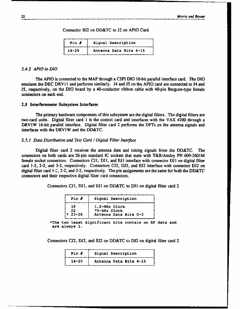
Connector BJ2 on DD&TC to J2 on APIO Card
Pin I Signal Description
14-25 Antenna Data Bits 4-15
2.4.2 APIO to DIO
The APIO is connected to the MAP through a CSPI DIO 16-bit parallel interface card. The DIOemulates the DEC DRV 1I and performs similarly. J4 and J5 on the APIO card are connected to J4 andJ5, respectively, on the DIO board by a 40-conductor ribbon cable with 40-pin Bergcon-type femaleconnectors on each end.
2.5 Interferometer Subsystem Interfaces
The primary hardware components of this subsystem are the digital filters. The digital filters aretwo-card units. Digital filter card 1 is the control card and interfaces with the VAX 4200 through aDRVIW 16-bit parallel interface. Digital filter card 2 performs the DFTs on the antenna signals andinterfaces with the DRVIW and the DD&TC.
2.5.1 Data Distribution and Test Card / Digital Filter Interface
Digital filter card 2 receives the antenna data and timing signals from the DD&TC. Theconnectors on both cards are 26-pin standard IC sockets that mate with T&B/Ansley PN 609-2601Mfemale socket connectors. Connectors CJ 1, DJ 1, and El I interface with connector DJ I on digital filtercard 1-2, 2-2, and 3-2, respectively. Connectors C02, DJ2, and EJ2 interface with connector DJ2 ondigital filter card I-C, 2-2, and 3-2, respectively. The pin assignments are the same for both the DD&TCconnectors and their respective digital filter card connectors.
Connectors CJ 1, D l, and ElI on DD&TC to DJ I on digital filter card 2
Pin # Signal Description
19 1.2-MHz Clock22 75-kHz Clock
* 23-26 Antenna Data Bits 0-3
*The two least significant bits contain no RF data andare always 1.
Connectors 02, DJ2, and EJ2 on DD&TC to DJ2 on digital filter card 2
Pin # Signal Description
14-25 Antenna Data Bits 4-15
NAVSPACECOM Spta Surveillance DSPR 4 23
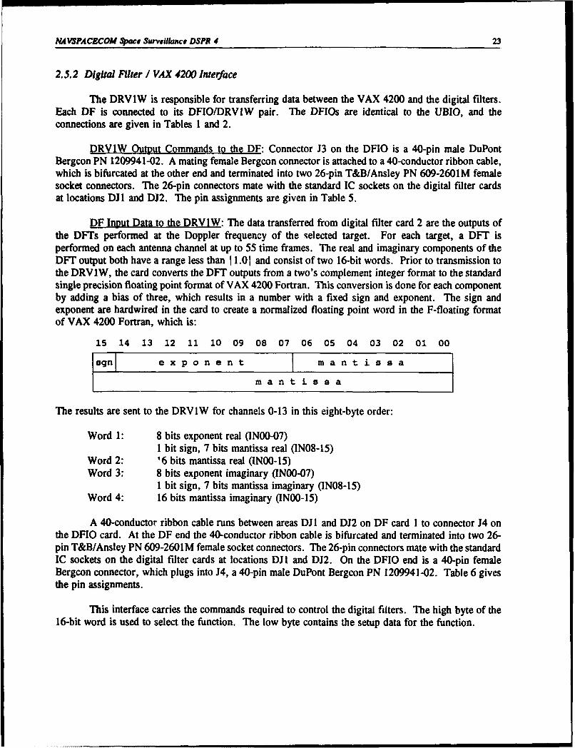
2.5.2 Digital Filter / VAX 4200 Interface
The DRV1W is responsible for transferring data between the VAX 4200 and the digital filters.Each DF is connected to its DFIO/DRVIW pair. The DFIOs are identical to the UBJO, and theconnections are given in Tables 1 and 2.
DRVIW Output Commands to the DF: Connector B3 on the DFIO is a 40-pin male DuPontBergcon PN 1209941-02. A mating female Bergcon connector is attached to a 40-conductor ribbon cable,which is bifurcated at the other end and terminated into two 26-pin T&B/Ansley PN 609-2601M femalesocket connectors. The 26-pin connectors mate with the standard IC sockets on the digital filter cardsat locations DJ I and DJ2. The pin assignments are given in Table 5.
DF Input Data to the DRV1W: The data transferred from digital filter card 2 are the outputs ofthe DFTs performed at the Doppler frequency of the selected target. For each target, a DFT isperformed on each antenna channel at up to 55 time frames. The real and imaginary components of theDFT output both have a range less than 11.01 and consist of two 16-bit words. Prior to transmission tothe DRV1W, the card converts the DFT outputs from a two's complement integer format to the standardsingle precision floating point format of VAX 4200 Fortran. This conversion is done for each componentby adding a bias of three, which results in a number with a fixed sign and exponent. The sign andexponent are hardwired in the card to create a normalized floating point word in the F-floating formatof VAX 4200 Fortran, which is:
15 14 13 12 11 10 09 08 07 06 05 04 03 02 01 00
sgn e x p o n e n t I m a n t i s s a
mantissa
The results are sent to the DRV1W for channels 0-13 in this eight-byte order:
Word 1: 8 bits exponent real (IN00-07)1 bit sign, 7 bits mantissa real (IN08-15)
Word 2: '6 bits mantissa real (INOO-15)Word 3: 8 bits exponent imaginary (INOO-07)
1 bit sign, 7 bits mantissa imaginary (IN08-15)Word 4: 16 bits mantissa imaginary (INOO-15)
A 40-conductor ribbon cable runs between areas DJ I and DJ2 on DF card 1 to connector J4 onthe DFIO card. At the DF end the 40-conductor ribbon cable is bifurcated and terminated into two 26-pin T&B/Ansley PN 609-2601M female socket connectors. The 26-pin connectors mate with the standardIC sockets on the digital filter cards at locations DJ I and DJ2. On the DFIO end is a 40-pin femaleBergcon connector, which plugs into J4, a 40-pin male DuPont Bergcon PN 1209941-02. Table 6 givesthe pin assignments.
This interface carries the commands required to control the digital filters. The high byte of the16-bit word is used to select the function. The low byte contains the setup data for the function.
24 Morris and Bryan
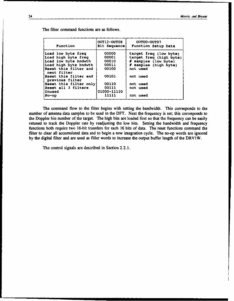
The filter command functions are as follows.
OUT12-OUT08 OUTOO-OUT07Function Bit Sequence Function Setup Data
Load low byte freq 00000 target freq (low byte)Load high byte freq 00001 target freq (high byte)Load low byte bndwth 00010 # samples (low byte)Load high byte bndwth 00011 # samples (high byte)Reset this filter and 00100 not usednext filter
Reset this filter and 00101 not usedprevious filter
Reset this filter only 00110 not usedReset all 3 filters 00111 not usedUnused 01000-11110No-op 11111 not used
The command flow to the filter begins with setting the bandwidth. This corresponds to thenumber of antenna data samples to be used in the DFT. Next the frequency is set; this corresponds tothe Doppler bin number of the target. The high bits are loaded first so that the frequency can be easilyretuned to track the Doppler rate by readjusting the low bits. Setting the bandwidth and frequencyfunctions both require two 16-bit transfers for each 16 bits of data. The reset functions command thefilter to clear all accumulated data and to begin a new integration cycle. The no-op words are ignoredby the digital filter and are used as filler words to increase the output buffer length of the DRV1W.
The control signals are described in Section 2.2.1.
NAVSPACECOM S)Pace Survwance DSPR 4 25
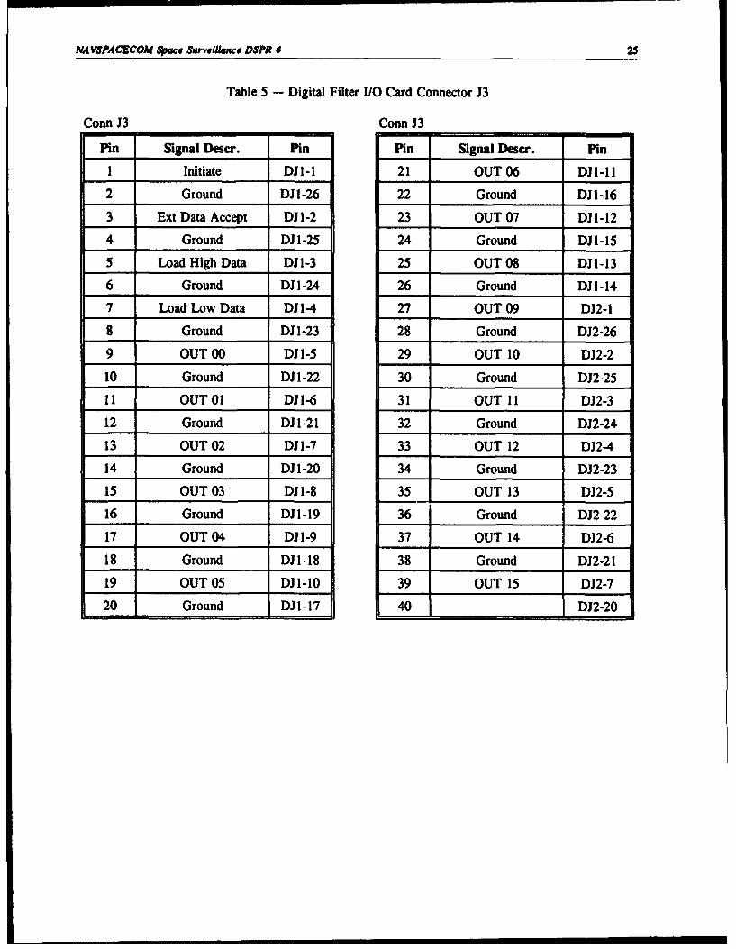
Table 5 - Digital Filter I/O Card Connector J3
Conn J3 Conn B3
Pin Signal Descr. Pin Pin Signal Descr. Pin
I Initiate DJI-1 21 OUT 06 DJI-II
2 Ground DJ1-26 22 Ground DJ1-16
3 Ext Data Accept DJ 1-2 23 OUT 07 DJ 1- 12
4 Ground DJI-25 24 Ground DJI-15
5 Load High Data DJ1-3 25 OUT 08 DJI-13
6 Ground DJ 1-24 26 Ground DJ 1-14
7 Load Low Data DJI 1-4 27 OUT 09 DJ2-1
8 Ground DJ 1-23 28 Ground DJ2-26
9 OUT 00 DJ 1-5 29 OUT 10 DJ2-2
10 Ground DJ 1-22 30 Ground DJ2-25
11 OUT 01 DJ1-6 31 OUT 11 DJ2-3
12 Ground DJ 1-21 32 Ground DJ2-24
13 OUT 02 DJ 1-7 33 OUT 12 DJ2-4
14 Ground DJ 1-20 34 Ground DJ2-23
15 OUT 03 DJ 1-8 35 OUT 13 DJ2-5
16 Ground DJ 1-19 36 Ground DJ2-22
17 OUT 04 DJ 1-9 37 OUT 14 DJ2-6
18 Ground DJI-18 38 Ground DJ2-21
19 OUT 05 DJI 1-10 39 OUT 15 DJ2-7
20 Ground DJ 1-17 40 DJ2-20
26 Morris and Bryant
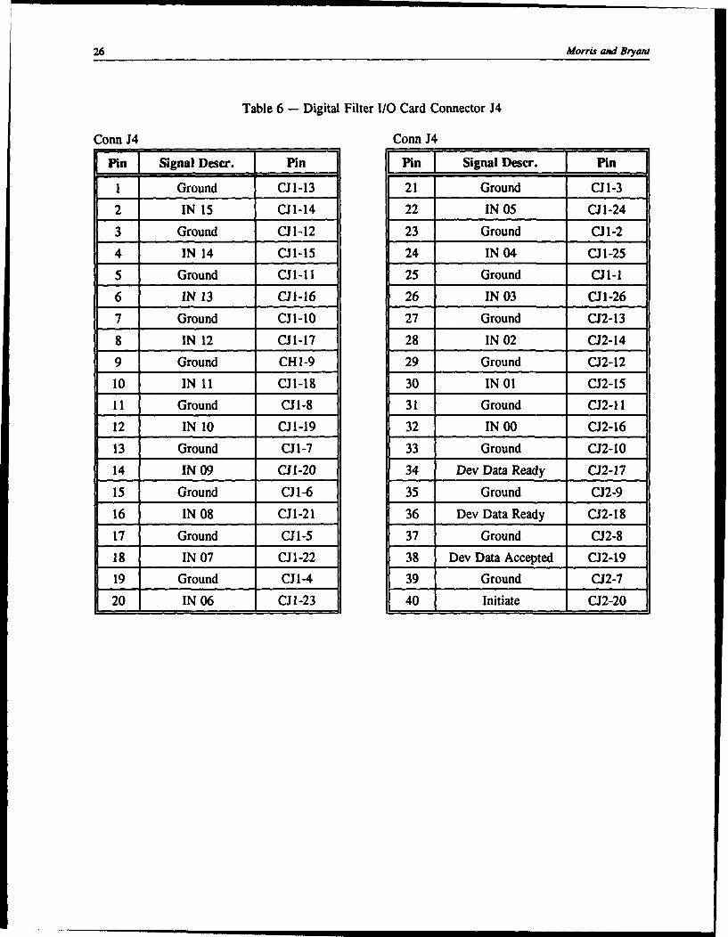
Table 6 - Digital Filter 1/0 Card Connector A4
Conn J4 Conn J4
Pin Signal Deser. Pin Pin I Signal Descr. Pin
I Ground CJ 1-13 21 Ground CJ 1-3
2 IN 15 CI- 14 22 IN 05 CJ1-24
3 Ground CJ 1-12 23 Ground CJ 1-2
4 IN 14 1-15 24 IN 04 CJ1-25
5 Ground 01-11 25 Ground CI1-1
6 IN 13 C11-16 26 IN 03 CJ1-26
7 Ground CI1-10 27 Ground C02-13
8 IN 12 CJI-17 28 IN 02 C02-149 Ground CH1-9 29 Ground C02-12
10 IN 11 CJI-18 30 IN 01 C2-15
11 Ground CJ 1-8 31 Ground CJ2-11
12 IN 10 CJ1-19 32 IN 00 02-16
13 Ground CJ 1-7 33 Ground C02-10
14 IN 09 CJI-20 34 Dev Data Ready CJ2-17
15 Ground CJ 1-6 35 Ground 02-9
16 IN 08 CJ1-21 36 Dev Data Ready 02-18
17 Ground CJ 1-5 37 Ground 02-8
18 IN 07 CJ1-22 38 Dev Data Accepted 02-19
19 Ground C0 1-4 39 Ground 02-7
20 IN 06 CJ1-23 40 Initiate 02-20
ASPACECOM Space Sw•,illance DSPR 4 27
2.6 Data Line Communications Subsystem Interfaces
The single hardware interface for this subsystem is described in Section 2.2.4.
2.7 Interprocessor Communications Subsystem Interfaces
The single hardware interface for this subsystem is described in Section 2.2.5.
2.8 Calibration and Diagnostics Subsystem Interfaces
The primary hardware component of this subsystem is the Hewlett-Packard (HP) 8565A SignalGenerator/Calibrator. The IEEE-488 bus is the interface between the central controller and the signalgenerator/calibrator and HP-lB clock. All items on the bus have the standard IEEE-488 bus interface.Listed below are the devices on the bus, the IEEE-488 interface connector, and the allowable modes ofoperation on the bus.
IEQ Defined FunctionsIEEE-488
Bus Device Conn Bus Sys Ctrlr Ctrlr-In-Chg Talk Listen
IEQ1l Bus Ctrlr Ji X X X XHP59309 HP-IB Clk A2J2 X XHP8565A Calibrator HP-IB X X
The IEQ 11 bus controller connects the Qbus to the IEEE-488 Bus. The bus is common to boththe primary and secondary systems, and each system has a connected IEQ 11. Connector J 1 is a 40-pinBergcon; an interface cable provides the standard IEC 25-pin connector. This connection is describedin Section 2.2.6. The bus system controller activates the "Interface Clear" (IFC) (pin 9) and the "RemoteEnable" (REN) (pin 17) control signals.
3. CRITICAL TIMING PATHS
Several data processing items in the DSPR system have critical timing paths. These include alertprocessing, interferometer data processing, and data communications to the Space Surveillance ProcessingCenter.
3.1 Target Detection and Selection Subsystem
IPocessing in this subsystem is time critical for two reasons. First, antenna data is fed to thissubsys,_-m and to the interferometer data collection subsystem simultaneously. Therefore, the targetselection process must be completed in the shortest time possible, so that the amount of data lost in theinterferometer subsystem is minimal. The primary system double buffers the data in the MAP 4000 andprocesses data in blocks of 2048 samples. At a 75-kHz sample rate, a buffer is ready for processingevery 27.3 ms. Consequently, the array processor must have finished its processing on the previousblock within this time. In the secondary system, data is double-buffered in blocks of 8192 samples,which take 109 ms to collect. A half-Doppler and quarter-Doppler detection cycle must be completedwithin this time. Summarized below are the steps involved in alert data processing and target selection.
The APIO card performs the alert data extraction and transmission in the following steps.

28 Morris and Bryat
1. Receive data from DD&TC2. Extract alert data3. Pass data to the MAP 4000 through the DIO as requested
3.2 System Timing Subsystem
The KWV II clock is used to obtain precise time for time stamping the observed data. Set tooperate at 10 kHz, the KWV1 I's counter increments every 0.1 ms. This counter is reset by the 1-pulse-per-second received from the HP 5061B Cesium Beam Time Standard. Each pulse generates an interruptfrom the KWV 11 to the central controller, which is used by a time stamp driver to update the softwareclock. Whenever interferometer data is time stamped, the hour, minute, and second are read from thesoftware clock. The fractional part of the second is read from the counter register of the KWVI 1.
Procedure CLOCK is assigned the task of keeping system time. At system startup, the softwareclock must be set by reading the HP 59309A digital clock. This procedure is given in Appendix E ofV olume 1 of this system description2.
3.3 Data Processing Subsystem
Processing in this subsystem is time critical for the data collection function. The maximum timerequired for the digital filters to process and output a complete cycle of data for each target is 1.0374seconds in the primary system. Because each filter operates independently, up to three targets can beprocessed simultaneously in a 1-second interval. However, the data reduction procedure can only processdata from one filter at a time. It is necessary that data reduction on three filter outputs is completed in1.0374 seconds. As a result, the computational time for the antenna data processing procedure isrestricted-to 300 ms. The data processing procedure in the central controller performs the antenna dataprocessing. This procedure is described in Section 6 of Volume 1 of this system description3.
3.4 Interferometer Data Collection Subsystem
All of the processing functions of this subsystem are time critical. Due to the short period of timethat a target is in the system, it is vital that data collection commence as soon as possible after targetselection. Also, the time stamp is formed after the reset command is given to the digital filter to beginprocessing. Hence, there will exist some delay between the time that the time stamp is formed and thereset command is interpreted by the digital filter. This time difference should be less than 0.1 ms sincethe KWVI I is accurate to this figure. Ideally, it should be less than 0.01 ms to minimize the likelihoodof the counter register incrementing while it is being read. GETTIME, the subroutine that time stampsthe interferometer data, raises its priority to the highest level to lock out other processes. GETTIMEreturns the priority to its normal level after reading the system time and the counter register of theKWV 11.
2 Carl J. Morris, Carolyn F. Bryant, Marilyn P. Earl, and Tamara A. Myers, NAVSPASUR Sensor System
Digital Signal Processing Receiver, Volume 1--Hardware and Software Overview, NRL/FR/8154--93-9577, Sept.1993.
3 Ibid.

?MVSPACECOM Space SwwiUawce DSPR 4 29
4. HIGH-ALTITUDE SYSTEM
This section describes the hardware differences between the low-altitude and high-altitude receiverstations. The hardware configuration of the high-altitude stations is very similar to that of the low-altitude(normal) stations, but with greater detection capability due to a larger, more sensitive antenna field. Thisantenna field allows detection of smaller or more distant orbiting objects.
4.1 RF Subsystem
The high-altitude station has 11 antenna arrays and two alert signals, designated as East Alert andWest Alert. A spare channel brings the number of receiver channels required to 14. This is the samenumber required for the low-altitude station, which has 12 antenna arrays, one alert signal, and one sparechannel. Consequently, the signal processing within the subsystem is identical between the two stations.
4.2 Target Detection and Selection Subsystem
Because the high-altitude stations have two alert channels, the capacity for twice the alertprocessing within the same time period is required. This increased capacity is accomplished by using twoAPIOs and two CSPI MAP 4000 array processors for each system. Figure 4 shows the configuration.
~AP Bus
P..........0
S~ Antenna
0. Data
Fig. 4--High-altitude alert interconnections
"-- m m I I l l ~ l i m m Elilnl
30 Morris and Bryat
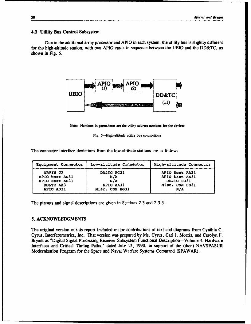
4.3 Utility Bus Control Subsystem
Due to the additional array processor and APIO in each system, the utility bus is slightly differentfor the high-altitude station, with two APIO cards in sequence between the UBIO and the DD&TC, asshown in Fig. 5.
(1) 0 (2)UBIO DD&TC
km109 7(11)TN
Note: Numbers in parentheses are the utility address numbers for the devices
Fig. 5-High-altitude utility bus connections
The connector interface deviations from the low-altitude stations are as follows.
Equipment Connector Low-altitude Connector High-altitude Connector
DRVlW J2 DD&TC BG31 APIO West AA31APIO West AD31 N/A APIO East AA31APIO East AD31 N/A DD&TC BG31
DD&TC AA3 APIO AA31 Misc. CSM BG31APIO AD31 Misc. CSM BG31 N/A
The pinouts and signal descriptions are given in Sections 2.3 and 2.3.3.
5. ACKNOWLEDGMENTS
The original version of this report included major contributions of text and diagrams from Cynthia C.Cyrus, Interferometrics, Inc. That version was prepared by Ms. Cyrus, Carl J. Morris, and Carolyn F.Bryant as "Digital Signal Processing Receiver Subsystem Functional Description-Volume 4: HardwareInterfaces and Critical Timing Paths," dated July 15, 1990, in support of the (then) NAVSPASURModernization Program for the Space and Naval Warfare Systems Command (SPAWAR).
44V$AC5UCOW 4.ow Swwawe DSpR 4 31
ACRONYMS AND ABBREVIATIONS
A/D analog-to-digitalAPIO array processor input/outputCSM command status modulesDD&TC data distribution and test cardDEC Digital Equipment CorporationDF digital filterDFIO digital filter input/outputDFT discrete Fourier transformDIO direct input/outputDSPR Digital Signal Processing ReceiverHINT host interfaceHP Hewlett-PackardIC integrated circuitICC interprocessor communications
(formerly inter-controller communications)I/O input/outputkHz kilohertzLO local oscillatorMAP MAP 4000 Array ProcessorMHz megahertzms millisecondsNAVSPACECOM Naval Space Command
(formerly Naval Space Surveillance (NAVSPASUR))NRL Naval Research LaboratoryOPTEST operational testPN part numberpps pulse per secondRF radio frequencySPADATS Space Detection and Tracking SystemTRGSEL Target SelectionUB utility busUBIO utility bus input/output