NANOSENSORS ENGINEERING: II. SUPERFICIAL FUNCTIONALIZATION OF SnO2
13
NANOSENSORS ENGINEERING: II. SUPERFICIAL FUNCTIONALIZATION OF SnO 2 NANOWIRE FOR SENSING PERFORMANCE IMPROVEMENT Serghei Dmitriev Physics Department, Moldova State University 60, A. Mateevici str., Chisinau, MD-2009, Moldova E-mail: [email protected] Abstract - Paper presents results of study aimed the tin dioxide nanowire gas sensing performance improvement via in situ functionalization with NiO. Developed nanostructures have demonstrated improved by order gas sensitivity toward H 2 and CO and drastic increase of selectivity to H 2 against CO. Obtained results are discussed from the point of view of NiO/SnO 2 heterojunction formation and its influence on electrical transport through nanowire and nanowire interaction with target gases. Key words: Nanowire, tin dioxide, nickel oxide, chemoresistor, functionalization, heterojunction I. INTRODUCTION Chemical nanosensors represent high interest for researchers and manufacturers in the field of gas sensorics due to their potential to detect very low concentrations of active impurities in atmosphere [1-5]. Capability to detect low concentrations of target gases is connected usually with extremely high surface-to-volume ratio of given nanostructures as their electrical characteristics are highly sensitive to surface-adsorbed gaseous species. However, the problem of selectivity of low-dimensional gas sensitive structures remains and on the nanoscopic level. There are known some attempts to improve gas sensing performance through the electron density manipulation in the nanodimensional structures (NDS) using UV irradiation [6] or nanowire configured as field effect transistor (FET) [7]. The attempt to functionalize polysilicon mesowire using Pd is well described in [8], however, for H 2 sensor there was used multi-step INTERNATIONAL JOURNAL ON SMART SENSING AND INTELLIGENT SYSTEMS, VOL. 3, NO. 4, DECEMBER 2010 807
Transcript of NANOSENSORS ENGINEERING: II. SUPERFICIAL FUNCTIONALIZATION OF SnO2
NANOSENSORS ENGINEERING:
II. SUPERFICIAL FUNCTIONALIZATION OF SnO2
NANOWIRE FOR SENSING PERFORMANCE IMPROVEMENT
Serghei Dmitriev
Physics Department, Moldova State University
60, A. Mateevici str., Chisinau, MD-2009, Moldova
E-mail: [email protected]
Abstract - Paper presents results of study aimed the tin dioxide nanowire gas sensing
performance improvement via in situ functionalization with NiO. Developed nanostructures
have demonstrated improved by order gas sensitivity toward H2 and CO and drastic increase of
selectivity to H2 against CO. Obtained results are discussed from the point of view of
NiO/SnO2 heterojunction formation and its influence on electrical transport through
nanowire and nanowire interaction with target gases.
Key words: Nanowire, tin dioxide, nickel oxide, chemoresistor, functionalization, heterojunction
I. INTRODUCTION
Chemical nanosensors represent high interest for researchers and manufacturers in the field
of gas sensorics due to their potential to detect very low concentrations of active impurities in
atmosphere [1-5]. Capability to detect low concentrations of target gases is connected usually
with extremely high surface-to-volume ratio of given nanostructures as their electrical
characteristics are highly sensitive to surface-adsorbed gaseous species. However, the problem of
selectivity of low-dimensional gas sensitive structures remains and on the nanoscopic level.
There are known some attempts to improve gas sensing performance through the electron density
manipulation in the nanodimensional structures (NDS) using UV irradiation [6] or nanowire
configured as field effect transistor (FET) [7]. The attempt to functionalize polysilicon mesowire
using Pd is well described in [8], however, for H2 sensor there was used multi-step
INTERNATIONAL JOURNAL ON SMART SENSING AND INTELLIGENT SYSTEMS, VOL. 3, NO. 4, DECEMBER 2010
807
micromachining process. At that Pd was deposited along of all top side of polysilicon nanowire,
forming practically continuous thin film on the NW surface. The resulting nanodevice was
metal/semiconductor Schottky diode. Another approach was demonstrated in [9], where Pd was
deposited already as particles on the surface of SnO2 NW.
Here we report an approach to SnO2 nanowire gas sensing performance improvement based
on in situ nanowire surface functionalization with NiOx clusters. In essence, the task is to format
the multitude nanodimensional p-n heterojunctions on the surface of such nanostructure as
nanowire. Nickel oxide, in its non-stoichiometric NiOx form, in contrast to metallic palladium, is
semiconducting material of p-type conductivity. It is intriguing from the physical point of view
material due to its useful catalytic [10-12], magnetic [13], optical [14] and electrochromic
properties [15]. In less degree, nickel oxide is known as gas sensing material [16-20].
As to SnO2 it is well known and wide used n-type semiconducting gas sensitive material with
wide band-gap (3.6 eV) with the rutile structure [21]. Electrical conductivity in tin oxide is result
of non-stoichiometry stipulated basically by point atomic defects (oxygen vacancies). Single and
double charged oxygen vacancies form two levels in forbidden zone - 30 meV and 150 meV
correspondingly - below conductance band [22]. Additional levels arise at the chemisorption of
gaseous molecules on the surface of semiconductor that leads to the space charge region
alteration and band bending changing. These phenomena are accompanied with conductivity
modulation. Deposition of the p-type NiOx clusters on the surface of SnO2 NW can dramatically
change the character of NW interaction with gases due to the formation of multitude local
NiO(p)-SnO2(n) heterojunctions on NW surface.
II. EXPERIMENTAL AND METHODS
a) General
Rutile structured SnO2 had been obtained as nanowire on Si/SiO2 substrate through the
standard vapor-solid procedure [23] at temperature T=900oC from SnO powder as precursor.
Argon gas of research purity was used as carrier gas in the tin dioxide nanowire grown process.
X-ray diffraction (XRD) study and Scanning Electron Microscopy (SEM) were used to
characterize the structure, composition and shape of the SnO2 NWs.
Serghei Dmitriev, NANOSENSORS ENGINEERING: II. SUPERFICIAL FUNCTIONALIZATION OF SnO2 NANOWIRE FOR SENSING PERFORMANCE IMPROVEMENT
808
Successive Ti/Au (20/500 nm) PVD deposition through the shadow mask in high vacuum
was used to produce electrical contacts to individual NWs. As fabricated SnO2 nanowire based
chemoresistor was mounted in UHV chamber with electrical feed-through and gas delivering
system governed by the computer.
Chemoresistor’s electrical characteristics (I-V curves) were measured in two-point
configuration under vacuum conditions. Gas sensing response toward inflammable (H2)
(PH2=3x10⁻⁴ Torr) and toxic (CO) (PCO=3x10⁻⁴ Torr) gases was measured with oxygen
background (PO2=1x10⁻⁴ Torr). The chemoresistor was kept at T=350oC for all electrical and gas
sensing measurements.
b) SnO2 nanowire functionalization
Before exposing chemoresistor to Ni flux the system was pumped to vacuum conditions
P=1x10⁻⁶ Torr and nanowire was exposed to UV light for 30 minutes for NW surface cleaning of
residue gases. Functionalization process was performed under the 6x10⁻⁶ Torr vacuum conditions
through standard PVD process. Sample’s temperature was kept at that at T=350oC. Ni deposition
process was controlled through the chemoresistor conductance change monitoring by computer.
For the process of in situ functionalization with NiOx there was used the deposition -
electrical - gas sensitive measurement cycle. Deposition time for NiOx was determined from
preliminary experiments, and has amounted 500 seconds per deposition. The deposition process
itself was repeated four times and it has been traced via controlling the NW current changing.
After deposition had ceased nanowire was subjected to pulses of H2 (PH2=3x10⁻⁴ Torr)
(inflammable gas) and CO (PCO=5x10⁻⁵ Torr) (toxic gas) with O2 background (PO2=1x10⁻⁴ Torr).
Considering the SnO2 functionalization with NiOx we should note that for its deposition there
was used metal Ni. At that we took into account that fact that Ni can be oxidized at sufficiently
low temperature even in the vacuum condition interacting with residual oxygen (P=6x10⁻⁶ Torr).
Briefly, we supposed that in our case the Ni deposited on the NW surface will transform into the
NiOx. We say NiOx because in reality the oxidation of Ni is not complete even at atmospheric
pressure and huge amount of oxygen vacancies is presented in the material, providing its
semiconducting properties (pure NiO is isolator). To verify this idea we deposited Ni between
another two pads (which were under the small voltage) to form a film. We had been continued
deposition process before current between these two pads has appeared. If as-grown film is really
INTERNATIONAL JOURNAL ON SMART SENSING AND INTELLIGENT SYSTEMS, VOL. 3, NO. 4, DECEMBER 2010
809
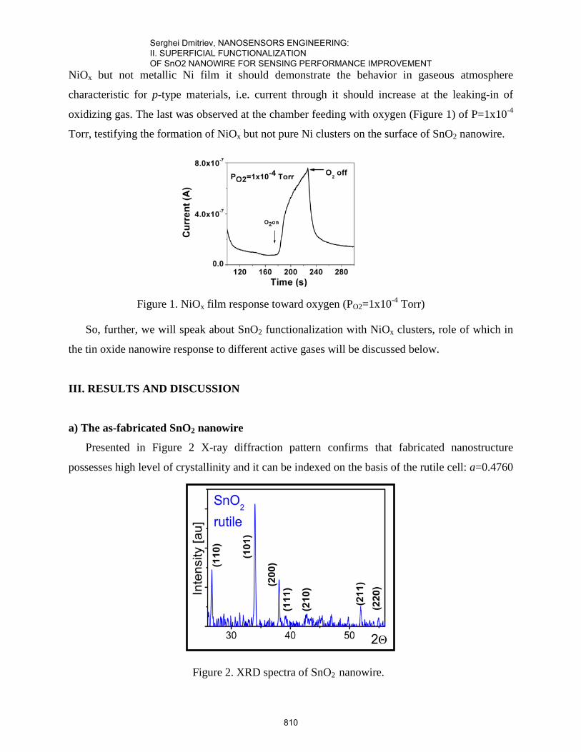
NiOx but not metallic Ni film it should demonstrate the behavior in gaseous atmosphere
characteristic for p-type materials, i.e. current through it should increase at the leaking-in of
oxidizing gas. The last was observed at the chamber feeding with oxygen (Figure 1) of P=1x10⁻⁴
Torr, testifying the formation of NiOx but not pure Ni clusters on the surface of SnO2 nanowire.
So, further, we will speak about SnO2 functionalization with NiOx clusters, role of which in
the tin oxide nanowire response to different active gases will be discussed below.
III. RESULTS AND DISCUSSION
a) The as-fabricated SnO2 nanowire
Presented in Figure 2 X-ray diffraction pattern confirms that fabricated nanostructure
possesses high level of crystallinity and it can be indexed on the basis of the rutile cell: a=0.4760
Figure 2. XRD spectra of SnO2 nanowire.
Figure 1. NiOx film response toward oxygen (PO2=1x10⁻⁴ Torr)
Serghei Dmitriev, NANOSENSORS ENGINEERING: II. SUPERFICIAL FUNCTIONALIZATION OF SnO2 NANOWIRE FOR SENSING PERFORMANCE IMPROVEMENT
810
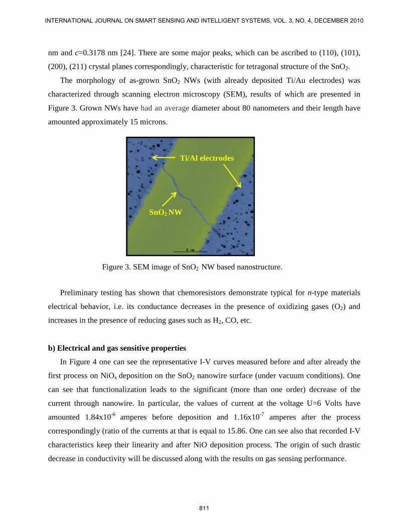
nm and c=0.3178 nm [24]. There are some major peaks, which can be ascribed to (110), (101),
(200), (211) crystal planes correspondingly, characteristic for tetragonal structure of the SnO2.
The morphology of as-grown SnO2 NWs (with already deposited Ti/Au electrodes) was
characterized through scanning electron microscopy (SEM), results of which are presented in
Figure 3. Grown NWs have had an average diameter about 80 nanometers and their length have
amounted approximately 15 microns.
Preliminary testing has shown that chemoresistors demonstrate typical for n-type materials
electrical behavior, i.e. its conductance decreases in the presence of oxidizing gases (O2) and
increases in the presence of reducing gases such as H2, CO, etc.
b) Electrical and gas sensitive properties
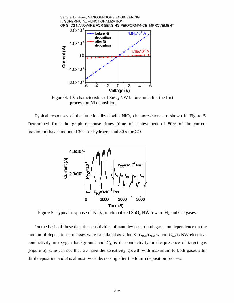
In Figure 4 one can see the representative I-V curves measured before and after already the
first process on NiOx deposition on the SnO2 nanowire surface (under vacuum conditions). One
can see that functionalization leads to the significant (more than one order) decrease of the
current through nanowire. In particular, the values of current at the voltage U=6 Volts have
amounted 1.84x10⁻⁶ amperes before deposition and 1.16x10⁻⁷ amperes after the process
correspondingly (ratio of the currents at that is equal to 15.86. One can see also that recorded I-V
characteristics keep their linearity and after NiO deposition process. The origin of such drastic
decrease in conductivity will be discussed along with the results on gas sensing performance.
Ti/Al electrodes
SnO2 NW
Figure 3. SEM image of SnO2 NW based nanostructure.
INTERNATIONAL JOURNAL ON SMART SENSING AND INTELLIGENT SYSTEMS, VOL. 3, NO. 4, DECEMBER 2010
811
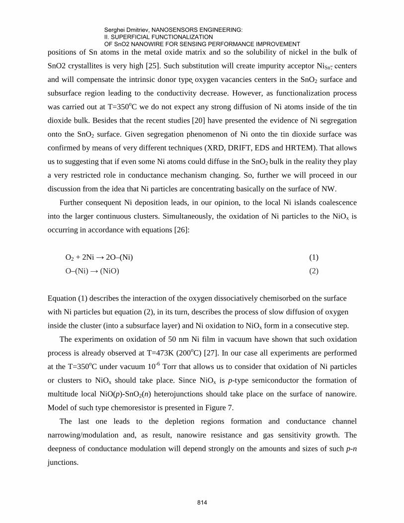
Typical responses of the functionalized with NiOx chemoresistors are shown in Figure 5.
Determined from the graph response times (time of achievement of 80% of the current
maximum) have amounted 30 s for hydrogen and 80 s for CO.
On the basis of these data the sensitivities of nanodevices to both gases on dependence on the
amount of deposition processes were calculated as value S=Ggas/GO2 where GO2 is NW electrical
conductivity in oxygen background and GR is its conductivity in the presence of target gas
(Figure 6). One can see that we have the sensitivity growth with maximum to both gases after
third deposition and S is almost twice decreasing after the fourth deposition process.
Figure 5. Typical response of NiOx functionalized SnO2 NW toward H2 and CO gases.
0 1000 2000 3000
2.0x10⁻⁸
4.0x10⁻⁸
P O2=
10-4 PCO=3x10⁻⁴ Torr
Curr
ent (
A)
Time (S)
PH2=3x10⁻⁴ Torr
Figure 4. I-V characteristics of SnO2 NW before and after the first process on Ni deposition.
-6 -4 -2 0 2 4 6-2.0x10⁻⁶
-1.0x10⁻⁶
0.0
1.0x10⁻⁶
2.0x10⁻⁶
1.16x10⁻⁷ A
before Ni deposition
after Ni deposition
Curr
ent (
A)
Voltage (V)
1.84x10⁻⁶ A
Serghei Dmitriev, NANOSENSORS ENGINEERING: II. SUPERFICIAL FUNCTIONALIZATION OF SnO2 NANOWIRE FOR SENSING PERFORMANCE IMPROVEMENT
812

Observed behavior we connect with the transformation of numerous and separated NiO
clusters on SnO2 NW surface in the regions of nanodimensional continuous film which:
1) are shunting the current through SnO2 NW due to the percolation effects and
2) are decreasing the SnO2 NW surface area open for interaction with gaseous species in air.
Another feature of the obtained data is connected with interaction of functionalized SnO2
NW with CO gas. In the case of NiOx functionalization sensitivity to CO (SCO) repeats the shape
of sensitivity to H2 (SH2) although is lower.
c) Electrical and gas sensing performance results analysis
Starting discussion of obtained results, we should note that at least three processes can take
place on the surface of SnO2 nanowire at the functionalization with NiOx:
1) Ni atoms interaction with SnO2 NW matrix and their incorporation in it;
2) Superficial Ni interaction with residual oxygen in the vacuum chamber and following
oxidation to NiOx;
3) NiO molecules/NiOx particles coalescence to the NiOx clusters on the SnO2 NW surface.
As to the first process, the positioning of the Ni atoms - on the surface or in the bulk of oxide
material – it remains still under the question. As the value of Ni2+ ionic radius (0.70Ǻ) is very
close to that of Sn4+ (0.69 Ǻ), it was suggested that Ni atoms are most likely to be located in the
Figure 6. Sensitivities of NiO functionalized SnO2 NW as function of the number of depositions.
INTERNATIONAL JOURNAL ON SMART SENSING AND INTELLIGENT SYSTEMS, VOL. 3, NO. 4, DECEMBER 2010
813
positions of Sn atoms in the metal oxide matrix and so the solubility of nickel in the bulk of
SnO2 crystallites is very high [25]. Such substitution will create impurity acceptor NiSn” centers
and will compensate the intrinsic donor type oxygen vacancies centers in the SnO2 surface and
subsurface region leading to the conductivity decrease. However, as functionalization process
was carried out at T=350oC we do not expect any strong diffusion of Ni atoms inside of the tin
dioxide bulk. Besides that the recent studies [20] have presented the evidence of Ni segregation
onto the SnO2 surface. Given segregation phenomenon of Ni onto the tin dioxide surface was
confirmed by means of very different techniques (XRD, DRIFT, EDS and HRTEM). That allows
us to suggesting that if even some Ni atoms could diffuse in the SnO2 bulk in the reality they play
a very restricted role in conductance mechanism changing. So, further we will proceed in our
discussion from the idea that Ni particles are concentrating basically on the surface of NW.
Further consequent Ni deposition leads, in our opinion, to the local Ni islands coalescence
into the larger continuous clusters. Simultaneously, the oxidation of Ni particles to the NiOx is
occurring in accordance with equations [26]:
O2 + 2Ni → 2O–(Ni) (1)
O–(Ni) → (NiO) (2)
Equation (1) describes the interaction of the oxygen dissociatively chemisorbed on the surface
with Ni particles but equation (2), in its turn, describes the process of slow diffusion of oxygen
inside the cluster (into a subsurface layer) and Ni oxidation to NiOx form in a consecutive step.
The experiments on oxidation of 50 nm Ni film in vacuum have shown that such oxidation
process is already observed at T=473K (200oC) [27]. In our case all experiments are performed
at the T=350oC under vacuum 10-6 Torr that allows us to consider that oxidation of Ni particles
or clusters to NiOx should take place. Since NiOx is p-type semiconductor the formation of
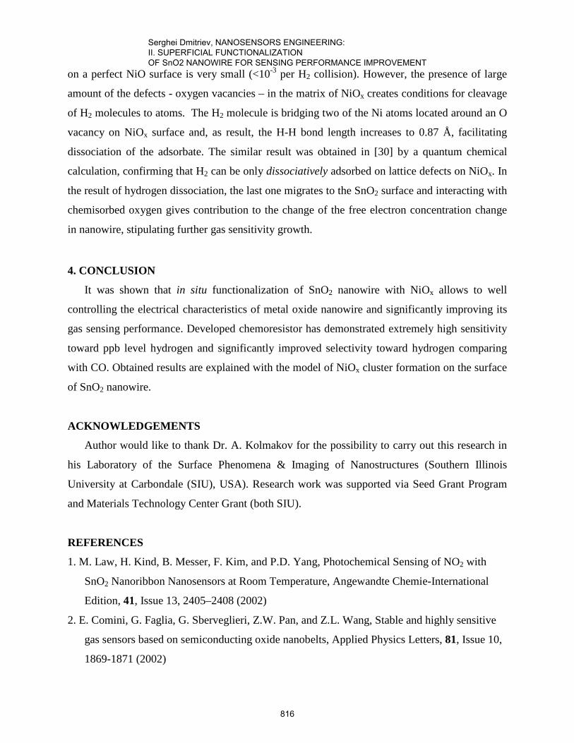
multitude local NiO(p)-SnO2(n) heterojunctions should take place on the surface of nanowire.
Model of such type chemoresistor is presented in Figure 7.
The last one leads to the depletion regions formation and conductance channel
narrowing/modulation and, as result, nanowire resistance and gas sensitivity growth. The
deepness of conductance modulation will depend strongly on the amounts and sizes of such p-n
junctions.
Serghei Dmitriev, NANOSENSORS ENGINEERING: II. SUPERFICIAL FUNCTIONALIZATION OF SnO2 NANOWIRE FOR SENSING PERFORMANCE IMPROVEMENT
814
Considering the NiOx clusters influence on sensitivities to the both gases we can see that
changes of the SH2 are more pronounced than in comparison with SCO as amount of depositions
grows. Such definite selectivity can be understood if to consider the reaction of NiO surface with
gaseous molecules of CO [28]:
NiO(s) + CO(g) ---> Ni(s) + CO2(g) (3)
where (s) and (g) mean solid and gas states correspondingly. It was shown that in given reaction,
yielding Ni atoms and CO2, there is a barrier of 15 kcal/mol relative to the reactants, occurring at
the second reaction step. Proceeding from that, nickel oxide material is expected to be less
efficient for oxidizing CO to CO2 [28]. Nickel oxide can also form the CONiO complex but the
latter would rather dissociate back to NiO + CO, requiring about 10 kcal/mol than to produce Ni
+ CO2 via the barrier of 25 kcal/mol. So, as result, the sensitivity of SnO2 NW functionalized
with NiO to CO gas is not so high in comparison with hydrogen.
As to sensitivity and selectivity to H2 we suggest here the next scheme of sensing. Along
with standard H2 interaction with tin dioxide surface the additional spillover effect takes place as
NiOx clusters provide the conditions for H2 molecules splitting [29]. In particular, it was shown
in given work both theoretically and experimentally (AES studies) that no reaction between H2
and the NiO(100) crystal after 50 min of exposure to the gas at 1x10⁻⁷ Torr and 350 °C, i.e. no
any significant changes in the O/Ni AES ratio. Thus, it was concluded that the probability for the
reaction
H2 (g)+ Ni-O (s) H2O (g) + Ni(s) (4)
SnO2 nanowire
NiO nanoclasters
depletion regions
ΔX
Figure 7. Model of the NiO(p)-SnO2(n) heterojunction type chemoresistor
INTERNATIONAL JOURNAL ON SMART SENSING AND INTELLIGENT SYSTEMS, VOL. 3, NO. 4, DECEMBER 2010
815
on a perfect NiO surface is very small (<10-3 per H2 collision). However, the presence of large
amount of the defects - oxygen vacancies – in the matrix of NiOx creates conditions for cleavage
of H2 molecules to atoms. The H2 molecule is bridging two of the Ni atoms located around an O
vacancy on NiOx surface and, as result, the H-H bond length increases to 0.87 Å, facilitating
dissociation of the adsorbate. The similar result was obtained in [30] by a quantum chemical
calculation, confirming that H2 can be only dissociatively adsorbed on lattice defects on NiOx. In
the result of hydrogen dissociation, the last one migrates to the SnO2 surface and interacting with
chemisorbed oxygen gives contribution to the change of the free electron concentration change
in nanowire, stipulating further gas sensitivity growth. 4. CONCLUSION
It was shown that in situ functionalization of SnO2 nanowire with NiOx allows to well
controlling the electrical characteristics of metal oxide nanowire and significantly improving its
gas sensing performance. Developed chemoresistor has demonstrated extremely high sensitivity
toward ppb level hydrogen and significantly improved selectivity toward hydrogen comparing
with CO. Obtained results are explained with the model of NiOx cluster formation on the surface
of SnO2 nanowire.
ACKNOWLEDGEMENTS
Author would like to thank Dr. A. Kolmakov for the possibility to carry out this research in
his Laboratory of the Surface Phenomena & Imaging of Nanostructures (Southern Illinois
University at Carbondale (SIU), USA). Research work was supported via Seed Grant Program
and Materials Technology Center Grant (both SIU).
REFERENCES
1. M. Law, H. Kind, B. Messer, F. Kim, and P.D. Yang, Photochemical Sensing of NO2 with
SnO2 Nanoribbon Nanosensors at Room Temperature, Angewandte Chemie-International
Edition, 41, Issue 13, 2405–2408 (2002)
2. E. Comini, G. Faglia, G. Sberveglieri, Z.W. Pan, and Z.L. Wang, Stable and highly sensitive
gas sensors based on semiconducting oxide nanobelts, Applied Physics Letters, 81, Issue 10,
1869-1871 (2002)
Serghei Dmitriev, NANOSENSORS ENGINEERING: II. SUPERFICIAL FUNCTIONALIZATION OF SnO2 NANOWIRE FOR SENSING PERFORMANCE IMPROVEMENT
816
3. C. Li, D.H. Zhang, X.L. Liu, S. Han, T. Tang, J. Han, and C.W. Zhou, In2O3 nanowires as
chemical sensors, Applied Physics Letters, 82, Issue 10, 1613 (2003)
4. A. Kolmakov, Y.X. Zhang, G.S. Cheng, and M. Moskovits, Detection of CO and O2 Using
Tin Oxide Nanowire Sensors, Advanced Materials, 15, 997 (2003)
5. A Maiti, J Rodriguez, M Law, P Kung, J McKinney, P Yang, SnO2 Nanoribons as NO2
Sensors, Nano Letters, 3, 1025-1028 (2003)
6. D. J. Zhang, C. Li, X. L. Liu, et al., Doping dependent NH3 sensing of indium oxide
nanowires, Applied Physics Letters, 83, 1845 (2003)
7. Y. Zhang, A. Kolmakov, S. Chretien, et al., Control of catalytic reactions at the surface of a
metal oxide nanowire by manipulating electron density inside it, Nano Letters, 4, 403 (2004)
8. A. Kolmakov, D.O. Klenov, Y. Lilach, S. Stemmer, and M. Moskovits, Enhanced Gas Sensing
by Individual SnO2 Nanowires and Nanobelts Functionalized with Pd Catalyst Particles,
Nano Letters, 5, 667 (2005)
9. M. Curreli, C. Li, Y. Sun, B. Lei, M.A. Gundersen, M.E. Thompson, C. Zhou, Selective
Functionalization of In2O3 Nanowire Mat Devices for Bio-sensing Applications, Journal of
the American Chemical Society, 127, 6922–6923 (2005)
10. A. Alejandre, F. Medina, P. Salagre, A. Fabregat, J.E. Sueiras, Characterization and activity
of copper and nickel catalysts for the oxidation of phenol aqueous solutions, Applied
Catalysis B-Environmental, 18, 307-315 (1998)
11. K. M. Dooley, S. Y. Chen, J. R. H. Ross, Stable Nickel-Containing Catalysts for the
Oxidative Coupling of Methane, J. Catal., 145, 402-408 (1994).
12. R. X. Dingsheng Wang, Xun Wang and Yadong Li, NiO nanorings and their unexpected
catalytic property for CO oxidation Nanotechnology, 17, 979–983 (2006)
13. R. H. Kodama, S. A. Makhlouf, A. E. Berkowitz, Finite Size Effects in Antiferromagnetic
NiO Nanoparticles, Physical Review Letters, 79, 1393 (1997)
14. T. M. H. Sato, S. Takata and T. Yamada, Transparent Conducting P-Type NiOx Thin Films
Prepared by Magnetron Sputtering, Thin Solid Films, 236, 27-31 (1993)
15. K. Yoshimura, T. Miki, and S. Tanemura, Nickel Oxide Electrochromic Thin Films Prepared
by Reactive DC Magnetron Sputtering, Japanese Journal of Applied Physics Part 1-Regular
Papers Short Notes & Review Papers, 34, 2440 (1995)
16. T. P. A.Neubecker, T. Doll, W. Hansch and I. Eisele, Ozone-enhanced molecular beam
INTERNATIONAL JOURNAL ON SMART SENSING AND INTELLIGENT SYSTEMS, VOL. 3, NO. 4, DECEMBER 2010
817

deposition of nickel oxide (NiO) for sensor applications, Thin Solid Films 310, 19-23 (1997)
17. J. H. I. Hotový, L. Spiess, R. Capkovic and S. Hascík, Preparation and characterization of
NiO thin films for gas sensor applications,.Vacuum, 58, 300 (2000)
18. M. Matsumiya, F. Qiu, W. Shin, N. Izu, N. Murayama, S. Kanzaki, Thin-film Li-doped NiO
for thermoelectric hydrogen gas sensor, Thin Solid Films, 419, 213 (2002)
19. V. R. I. Hotovy, P. Siciliano, S. Capone, L. Spiess, Sensing characteristics of NiO thin films
as NO2 gas sensor, Thin Solid Films, 418, 9 (2002)
20. R. C. P. Hidalgo, A.Coelho, and D. Gouvêa, Surface segregation and consequent SO2 sensor
response in SnO2-NiO, Chemistry of Materials, 17, 4149 (2005)
21. D.F.Cox, T.B. Fryberger, S. Semancik. Oxygen vacancies and defect electronic states on the
SnO2 (110)-1x1 surface, Physical Review B, 38, 2072-2083 (1988)
22. C.G.Founstadt, R.H.Rediker, Electrical Properties of High-Quality Stannic Oxide Crystals,
J.Appl. Phys, 42, 2911-2918 (1971)
23. Z.R. Dai, Z.W. Pan, and Z.L. Wang, Novel Nanostructures of Functional Oxides
Synthesized by Thermal Evaporation", Advanced Functional Materials, 13, 9, (2003)
24. McCarthy and J.Welton, Powder Diffraction, 4, 156 (1989)
25. M. N. Rumyantseva, O. V. Safonova, M. N. Boulova, L. I. Ryabova, A. M. Gas´kov, Russian
Chemical Bulletin, International Edition, Vol. 52, No. 6, pp. 1217—1238 ( 2003)
26. B. Monnerat, L. Kiwi-Minsker, A. Renken, Mathematical modelling of the unsteady-state
oxidation of nickel gauze catalysts, Chemical Engineering Science, 58, 4911–4919 (2003)
27. S. V.Kumari, M. Natarajan, V. K. Vaidyan, P. Koshy Surface oxidation of nickel thin films,
Journal of Materials Science Letters, 11, Iss.11, 761-762 (1992)
28. A.M. Mebel, D.-Y. Hwang, Theoretical Study on the Reaction Mechanism of Nickel Atoms
with Carbon Dioxide, J. Phys. Chem. A, 104 (49), pp 11622–11627, (2000)
29. J.A. Rodrigez, J.C.Hanson, A. I. Frenkel J.Y.Kim, M.Perez, Experimental and Theoretical
Studies on the Reaction of H2 with NiO: Role of O Vacancies and Mechanism of Oxide
Reduction, J.Am. Chem. Soc., 124, No.2, 346-354 (2002)
30. P.K. de Bokx, F. Labohm, O.L.J. Gijzeman, G.A. Bootsma, J.W. Geus, The Interaction of
Oxygen with Ni(100) and the Reduction of the Surface Oxide by Hydrogen, Appl. Surf. Sci.,
5, 321—331, (1980)
Serghei Dmitriev, NANOSENSORS ENGINEERING: II. SUPERFICIAL FUNCTIONALIZATION OF SnO2 NANOWIRE FOR SENSING PERFORMANCE IMPROVEMENT
818

INTERNATIONAL JOURNAL ON SMART SENSING AND INTELLIGENT SYSTEMS, VOL. 3, NO. 4, DECEMBER 2010
819