Nanoscience in Adolescence
101
Nanoscience in Adolescence George M. Whitesides Department of Chemistry and Chemical Biology Harvard University [email protected]
Transcript of Nanoscience in Adolescence

Nanoscience in Adolescence
George M. Whitesides
Department of Chemistry and Chemical Biology
Harvard University
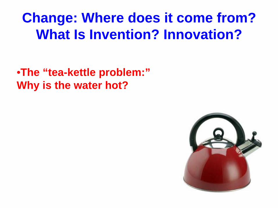
Change: Where does it come from? What Is Invention? Innovation?
•The “tea-kettle problem:” Why is the water hot?
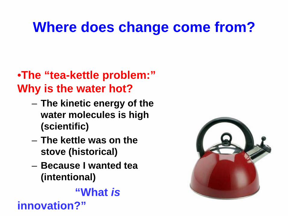
Where does change come from?
•The “tea-kettle problem:” Why is the water hot?
– The kinetic energy of the water molecules is high (scientific)
– The kettle was on the stove (historical)
– Because I wanted tea (intentional)
“What is innovation?”

How does a business exploit a new idea?
• Inventing fundamentally new products (U.S.)
• Developing better products, and engineering better ways of making them (Europe, Korea, Japan)
• Using inexpensive labor and low-cost capital to make lowest-cost products (China, India)
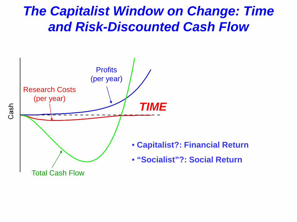
Research Costs (per year)
Profits (per year)
Total Cash Flow
The Capitalist Window on Change: Time and Risk-Discounted Cash Flow
TIME
• Capitalist?: Financial Return
• “Socialist”?: Social Return

All New Technologies: A Short, Qualitative History
Exaggerated expectations: exciting-sounding but irreproducible results and unrealistic claims.
Disappointment and (Over) reaction; Consolidation
Return to fundamentals; “discovery” and “science” in addition to technology and applications; development of new tools; large applications and real commercial investment.
Time
Expe
ctat
ions
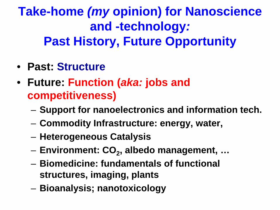
Take-home (my opinion) for Nanoscience and -technology:
Past History, Future Opportunity
• Past: Structure • Future: Function (aka: jobs and
competitiveness) – Support for nanoelectronics and information tech. – Commodity Infrastructure: energy, water, – Heterogeneous Catalysis – Environment: CO2, albedo management, … – Biomedicine: fundamentals of functional
structures, imaging, plants – Bioanalysis; nanotoxicology

At the Beginning: Expectations for Nano
• Applied Quantum Phenomena - Quantum computing • Futurist Speculations - Nanobots; The Assembler • Revolutionary Materials - Buckytubes and the space elevator - Quantum Dots • Revolutionary electronics - Single-molecule transistors - Ultradense computers • Biomedicine - “Nanotherapeutics” • Risks: - Nanobots, etc - Nanoparticle Toxicology
Drexler C&EN 2003

What is “nanoscience/technology”? • No universal definition • Dimensions are “small” (< 50 nm? < 20 nm?).
In popular terms “too small to see” (< 10 µm) • “Between molecules and macroscopic
matter” • New properties, especially room-temperature
quantum behavior (quantum dots) • Classical technology, but smaller than
current technology • “What I do” (whatever that is)
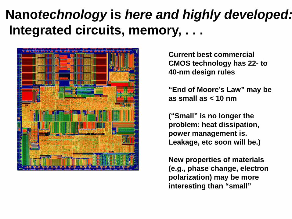
Nanotechnology is here and highly developed: Integrated circuits, memory, . . .
Current best commercial CMOS technology has 22- to 40-nm design rules “End of Moore’s Law” may be as small as < 10 nm (“Small” is no longer the problem: heat dissipation, power management is. Leakage, etc soon will be.) New properties of materials (e.g., phase change, electron polarization) may be more interesting than “small”
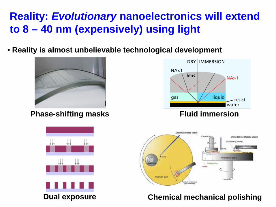
Reality: Evolutionary nanoelectronics will extend to 8 – 40 nm (expensively) using light
Phase-shifting masks Fluid immersion
Dual exposure Chemical mechanical polishing
• Reality is almost unbelievable technological development

Reality: New materials, but slow development of applications
• Buckytubes and maybe Graphene
• Quantum dots
• Other small particles
• (Nanoscale matter: grains, Interfaces, Debye layer, etc.)
M. Bawendi
Xu et. al. Nano Lett. 2004

Reality: Biomedical--Progress, but focused on conventional “high-technology” model
Medical Diagnostics
— Hydrophobic Nanoparticles — Transportation — Controlled Release
— Labeling — Imaging — Analyzing
Therapy
Challenges
— Volume-, tissue-, or cell-specific targeting — Remote guidance and activation — Safety Issues - biocompatibility and toxicity
Carbon nanotubes Quantum dots Magnetic nanoparticles Metal nanoparticles

Magnetite T. Hyeon Seoul National Univ.
Nanoparticles: MRI Contrast Agents
MRI = magnetic resonance imaging
A number of areas are approaching reality
• Buckytubes; graphene for electrically conductive plastics, perhaps electrochemical storage
• Low-cost methods of nanofabrication: printing, molding, others for consumer electronics, photovoltaics
• Optical systems for new optical effects, solid-state lighting, displays
• Nanoparticles/rods/cups/whatever with defined shapes for barcoding/tracking; delivery of hydrophobic drugs
• Nanometrology for industrial processing

Some Current Areas of Research: Examples in Fabrication
• Printing/molding • Phase-shifting lithography • 3D structures and Self-assembly • Nanoskiving • Holes • Optics
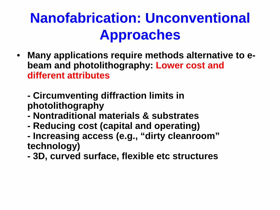
Nanofabrication: Unconventional Approaches
• Many applications require methods alternative to e-beam and photolithography: Lower cost and different attributes
- Circumventing diffraction limits in
photolithography - Nontraditional materials & substrates - Reducing cost (capital and operating) - Increasing access (e.g., “dirty cleanroom”
technology) - 3D, curved surface, flexible etc structures

Molding & Printing
Step-and-flash nanoimprinting
Willson & coworkers Macromolecules 2008
• Replace “mask” with “stamp” (“proximity” “contact”)
Isolated particles w/ low-γSL stamp
DeSimone & coworkers JACS 2005
Discrete TiO2 pillars
DeSimone & coworkers Adv. Mater. 2008
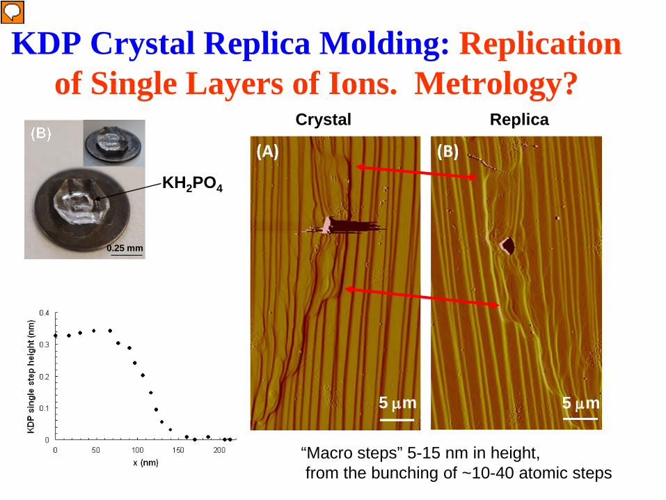
KDP Crystal Replica Molding: Replication of Single Layers of Ions. Metrology?
KH2PO4
0.25 mm
Crystal Replica
5 µm 5 µm
“Macro steps” 5-15 nm in height, from the bunching of ~10-40 atomic steps
簡報者
簡報註解
KDP = (potassium dihydrogen phosphate (KDP) – forms well defined Macro steps of varying height. Bottom left is an AFM lines scan of a single step on a crystal. This slide shows why we like KDP (it forms these macro steps of various height, so we can get lots of information in a single scan).
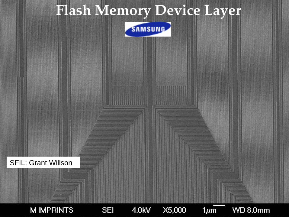
Gate Level: 38nm Half Pitch Flash Memory Device Layer
SFIL: Grant Willson

Phase-Separated Copolymers • Use photo-generated chemical patterns to direct block copolymer morphology
Stoykovich & Nealey Mater. Today 2006

If this works, it saves more than 100 unit process steps from the manufacturing of a modern microprocessor and provides a cost saving of 20-50% (per Infineon and SEMATECH. And Willson)
• Circumvents diffraction limits: physics limit < 0.01 nm; chemistry limit (granularity of matter) not understood
• Anomalously high resolution (<0.5 nm on open benchtop)
• 3D; eliminate process steps
• potential for roll-to-roll manufacturing: radical reduction in costs
• non-planar surfaces (soft lith; stretchy silicon)
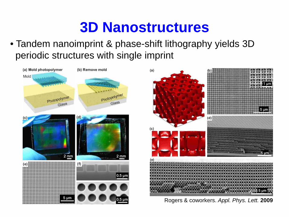
3D Nanostructures • Tandem nanoimprint & phase-shift lithography yields 3D periodic structures with single imprint
Rogers & coworkers. Appl. Phys. Lett. 2009
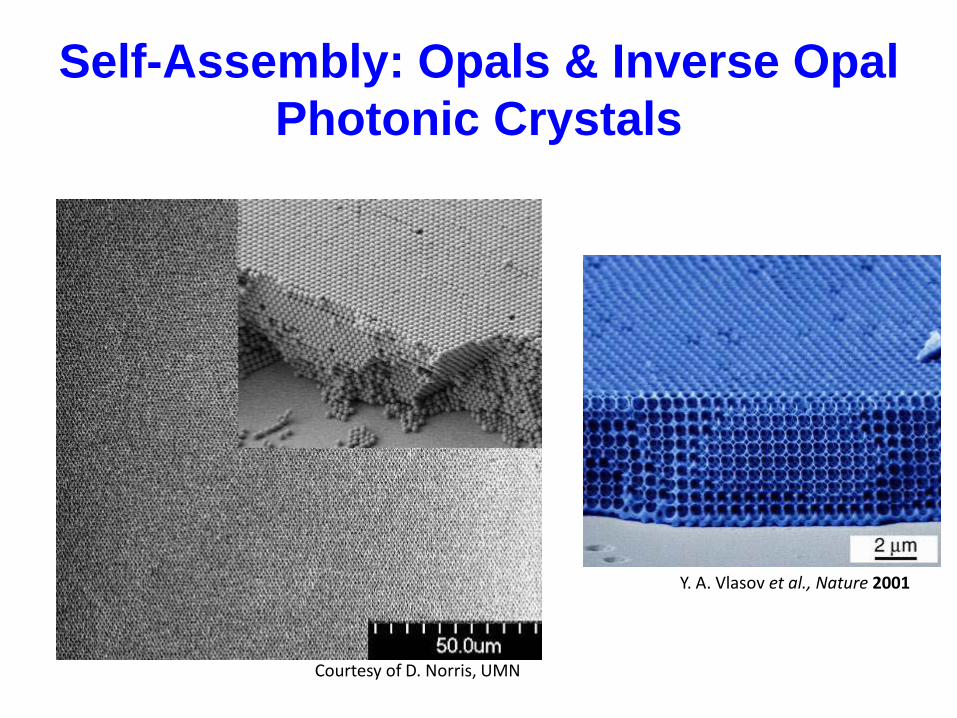
Self-Assembly: Opals & Inverse Opal Photonic Crystals
Courtesy of D. Norris, UMN
Y. A. Vlasov et al., Nature 2001

Nanoholes: Optofluidic Microscope • Slanted nanohole array • System resolution 490 nm
X. Heng, D. Erickson, L. R. Baugh, Z. Yaqoob, P. W. Sternberg, D. Psaltis, and C. Yang, Lab on a Chip 6, 1274 (2006). X. Cui, X. Heng, J. Wu, Z. Yaqoob, A. Scherer, D. Psaltis, and C. Yang, Optics Letters 31, 3161-3163 (2006).
Conventional microscope
Optofluidic microscope

Nanoskiving n. The use of an ultramicrotome for nanofabrication
Xu et al. Acc. Chem. Res. 2008

Gold Nanowires Generated by Sectioning Using a Microtome
10 nm wide 100 nm high nanowire on its edge
100 nm wide 10 nm high nanowire on its side

Fabrication of Complex 3-D Nanostructures
Template from diffraction gratings Template from periodic lines

Fabrication of Patterned Metallic Nanostructures over Large Areas
2 µm
View at an angle 35°
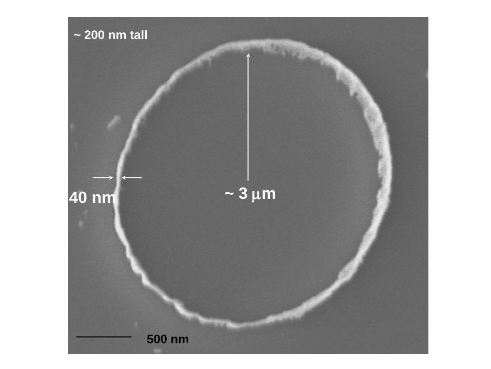
~ 200 nm tall
40 nm ~ 3 µm
500 nm


Some other Observations
• Nanotechnology now seen as a unifying field. Technologically useful? Yes. Technologically revolutionary? Not yet.
• The issues now are function and cost.
• For many important potential functions, we do not
know the rules. Heterogeneous catalysis, Nanotoxicology, Aerosols/albedo, Quantum isolation, Charge storage/transport/ interconversion, …
• We should answer the question: “Where does “nano” –rather than “micro” or just “small”—bring unique function or properties or behavior or cost?
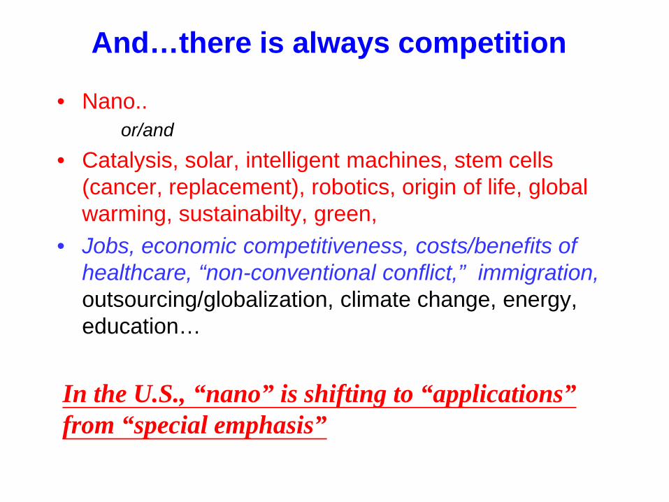
And…there is always competition
• Nano.. or/and
• Catalysis, solar, intelligent machines, stem cells (cancer, replacement), robotics, origin of life, global warming, sustainabilty, green,
• Jobs, economic competitiveness, costs/benefits of healthcare, “non-conventional conflict,” immigration, outsourcing/globalization, climate change, energy, education…
In the U.S., “nano” is shifting to “applications” from “special emphasis”
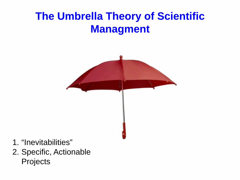
The Umbrella Theory of Scientific Managment
1. “Inevitabilities” 2. Specific, Actionable
Projects

Inevitabilities
• Areas where it is certain that society will need technology
• It may be too early to know what ultimate (or even initial) products are
• R&D should provide options, and early warning
• Examples: six (of perhaps 20) • Keys to success:
– Strategic selection, coupled with specificity – Critical mass in money, people – Patience (the www took 40 years; biotech still has
not happened)

1. Commodity Infrastructure: Energy, Water
• Supply/Demand-side technologies. • Honest, complete, accurate systems analysis • Biotechnology—finally a use? • Nanotechnology


Energy, Climate, Water, Sustainability
PeopleEnergyWellbeing ≈
Technology provides options to society
Options. •Generate more energy •Conserve the energy we now generate. •Have fewer people

Constraints
• Energy and Climate – Climate change may limit the combustion of fossil fuel
• Energy and Water
– Water production may become a major use of energy
• Energy and Nuclear – Weapons proliferation, reactor safety, waste
management
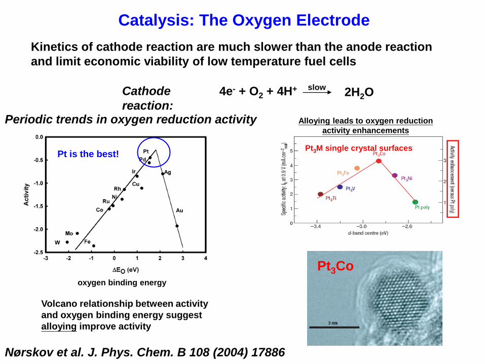
Catalysis: The Oxygen Electrode
4e- + O2 + 4H+ 2H2O slow
Kinetics of cathode reaction are much slower than the anode reaction and limit economic viability of low temperature fuel cells
Cathode reaction:
Nørskov et al. J. Phys. Chem. B 108 (2004) 17886
Periodic trends in oxygen reduction activity
oxygen binding energy
Volcano relationship between activity and oxygen binding energy suggest alloying improve activity
Pt is the best!
Alloying leads to oxygen reduction activity enhancements
Pt3M single crystal surfaces
Pt3Co

http://www.de.nec.de
Plasma Display
Diesel Fuel
spiral type compact fluorescent light bulb
Energy Conservation

Boeing 787. Approximately 50% carbon-epoxy composite. (Cost, autoclaves, damage, repair, electromagnetics/lightening, ….
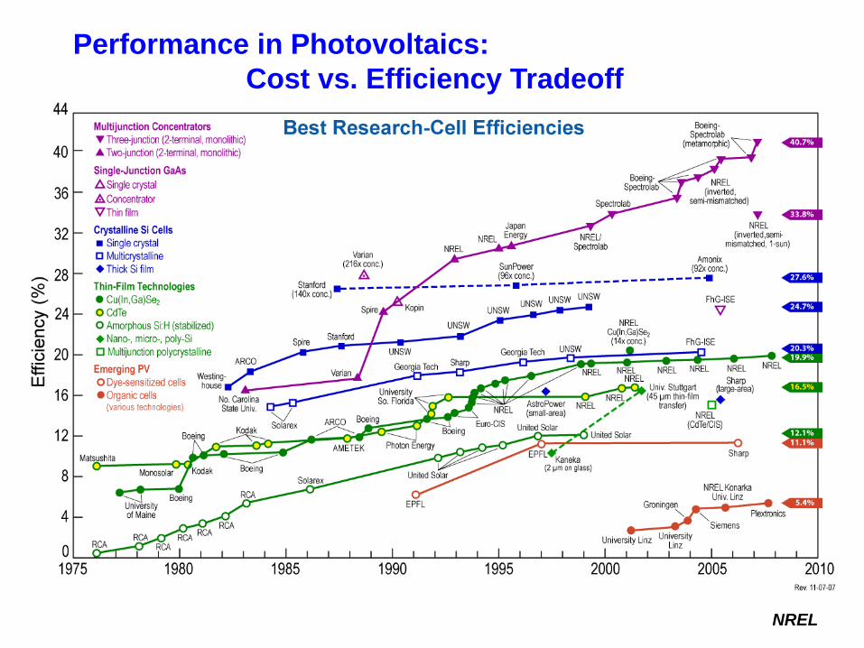
Performance in Photovoltaics: Cost vs. Efficiency Tradeoff
NREL

2. Global Stewardship
• CO2 and atmospheric management
• Population, “crowding”, future megacities • (Education)

“Geoengineering”
• Sulfuric Acid Sols – Tambora (1815) and the “year without a summer”
• CO2 for control
– Inject CO2 into atmosphere for “feedback” climate control

3. Information Technology
• Consumerization; globalization of information • Education, Entertainment

4. Health Care • Cost reduction: Prevention, Anticipation • Developing world • Is the patient important any more?
Vs.

5. Building the Global Middle Class
• The fusion of capitalism and socialism, with a 50- to 100-year time-scale
• National Security: Conflict and nation-building
Middle class in India

6. Robotics: Replacing Human Labor
BigDog, Boston Dynamics LittleDog, Boston Dynamics
http://www.bostondynamics.com/content/sec.php?section=BigDog http://www.bostondynamics.com/content/sec.php?section=LittleDog

A “Next Big Thing”
• Robotics: Changes the way we work. Work often defines what it is to be human.
• Investment: – Competition with low labor-rate competitors – Military
• Turing test

Robotics: Replacing Human Labor

1 µm
Fundamental/Basic Science: The Cell
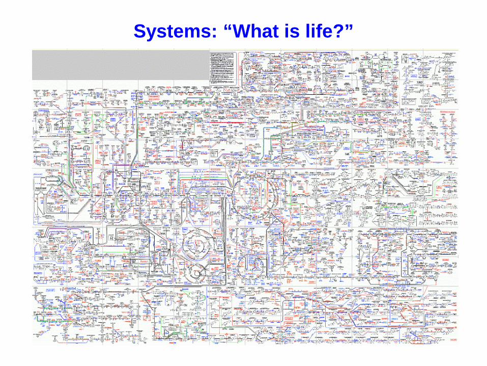
Systems: “What is life?”
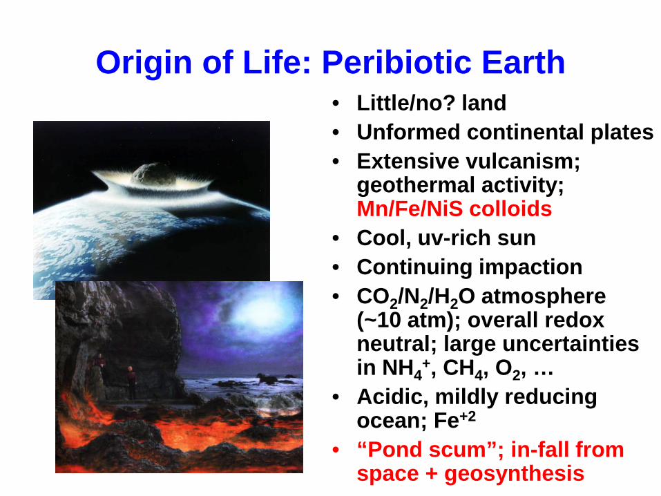
Origin of Life: Peribiotic Earth • Little/no? land • Unformed continental plates • Extensive vulcanism;
geothermal activity; Mn/Fe/NiS colloids
• Cool, uv-rich sun • Continuing impaction • CO2/N2/H2O atmosphere
(~10 atm); overall redox neutral; large uncertainties in NH4
+, CH4, O2, … • Acidic, mildly reducing
ocean; Fe+2
• “Pond scum”; in-fall from space + geosynthesis
Summary: Opportunities
• Nano has developed as integrative rather than revolutionary
• It is developing the tools needed to focus on function.
• Many connections to large-scale problems: Energy, water, climate change, health-care cost reduction, information technology
• Rich source of new materials and processes • Tools and concepts for fundamental science,
especially in catalysis, biology, charge-transport, optics, interfacial chemistry, materials science

For Nano and Nanochemistry, Fundamentals are Sound:
• Atoms/Molecules—”Nano”—Meso/Macro-scale Matter; the least-understood scale of matter.
• Charge transport (Energy generation/storage): occurs across nm-scale interfaces
• Assemblies in the cell are nanoscale • Heterogeneous catalysis: “catalysis by design” must
involve nano for empiricism to science • Surface science is nanoscale, and ubiquitous:
electrochemistry, plasmonics, membrane separations (RO/H2O, CO2, CH4), fuel cells/batteries/capacitors, solar cells
• The environment: Micro/nanoparticles, aerosols • New materials and characterization: Graphene, nanorods,
quantum dots, nanoresists, photovoltaics…SPM, tribology, corrosion, grain boundaries, phase-change materials

Some Generalizations about Nano: “Then” and “Now”
• Then – Generally: structure – “New” nanoelectronics – Nanosensors – Atomic/molecular-scale
visualization – “Nanomedicine” – The cell – “Nanobots”; the “self-
assembler”
• Now – Search for Function (Saalfeld
Criterion)—energy, consumer electronics, optics..
– Materials (graphene,..) – Nanoelectronics (materials
support) – Energy/sustainability/
climate/energy storage… – Search for applications in
biomedicine (NIH, VCs): imaging; research; environmental nano
– Search for a lead in heterogeneous catalysis

Acknowledgements
• Darren Lipomi • Roger York • Sindy Tang • Audrey Ellerbee (Stanford) • Zhihong Nie • Ben Wiley (Duke) • Qiaobing Xu • Michael Dickey (U. North Carolina) • Rob Rioux (Penn State)

Six big ideas 1. Applications: Electronics, Energy, Water 2. New materials 3. Information/globalization 4. The cell, biology, and medicine 5. Single atoms and molecules 6. Quantum phenomena, both fundamental
and applied

Opportunities: Lateral Transfer Electronics Chemistry
• Phase-shifting and immersion optics
• Spin-coating • Resists and thin films • Chemical vapor
deposition • Chemical mechanical
polishing • Si on oxide • High K materials
Opportunities: Lateral Transfer Chemistry Electronics
• Nanomolding • Buckytubes/nanotubes • High h+ mobility materials • Phase-change materials for electronics • Thin films; CVD
Opportunities: Energy
• Catalysis • Materials • Band-gap Engineering • Separations
----------------------- Energy: Thermal (high T is good) Electrochemistry (P = i2R = IV) Conservation Light weight, strong, corrosion resistant


http://www.de.nec.de/
Plasma Display
Diesel Fuel
spiral type compact fluorescent light bulb
Efficient Use of Energy
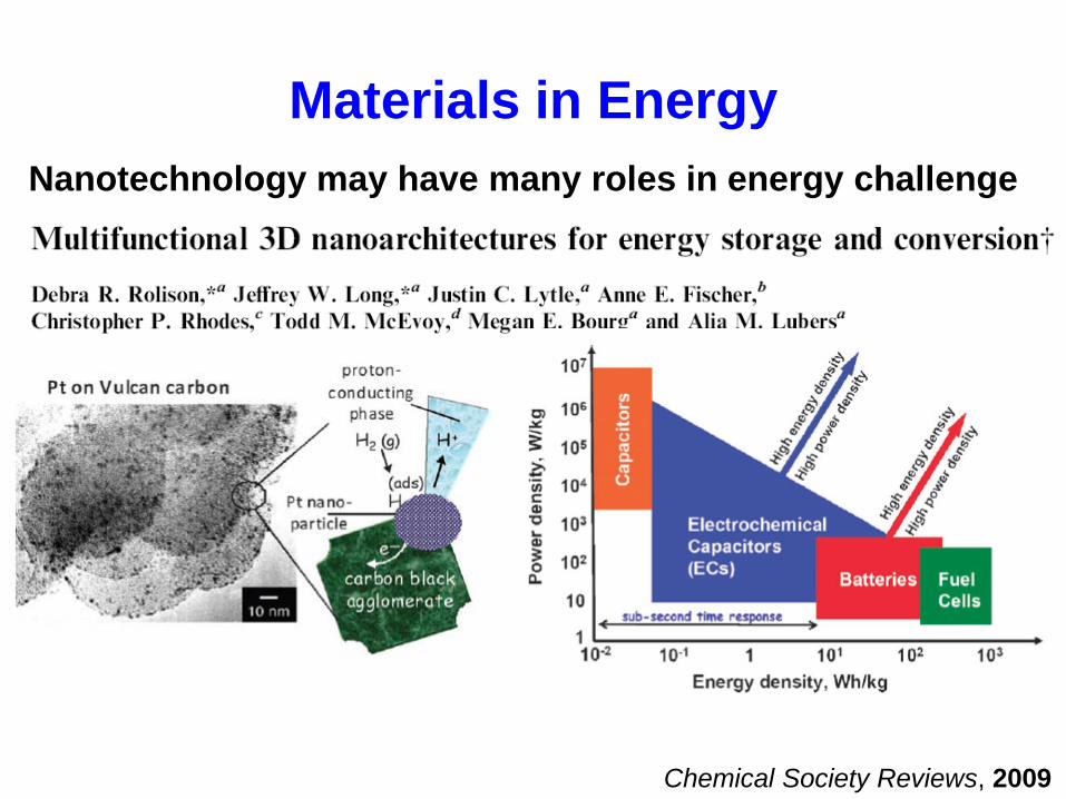
Materials in Energy
Chemical Society Reviews, 2009
Nanotechnology may have many roles in energy challenge

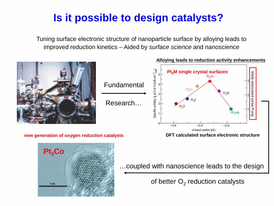
Is it Possible to Design Catalysts? Tuning surface electronic structure of nanoparticle surface by alloying leads to improved reduction kinetics – Aided by surface science and nanoscience
new generation of oxygen reduction catalysts DFT calculated surface electronic structure
Alloying leads to reduction activity enhancements
Pt3M single crystal surfaces
Fundamental
Research…
…coupled with nanoscience leads to the design
of better O2 reduction catalysts
Pt3Co

Nanoscience: Enabling Catalysis by Design
Particle size and shape is critical for activity and selectivity
•Relatively inert Au becomes active once the particle size reaches an optimal diameter. •Methods of surface science are still critical for understanding how catalyst operates, but the complexity of real catalysts must be integrated into model catalyst design
M. Valden et al. Science 281 (1998) 1647.

Supported Nanoparticles to Catalyze Reduction of O2 in Proton Exchange
Membrane Fuel Cells
anode cathode
2H2 4H+ + 4e- O2 + 4H+ + 4e-
2H2O
H+ H+
H+
H+
H+
H+
H+
H+
H+
H+
H2
O2
H2O
e- e-
Polymer membrane “electrolyte” (doped perfluorocarbon)
O2 reduction is the rate-limiting step…

Nanostructured Photovoltaic Cells • Solar materials - Cheap semiconductors (organics,
nanocrystals, etc.) have poor exciton and/or carrier lifetimes
- Nanostructuring is essential
100 – 200 nm
Ordered bulk heterojunction
10 – 20 nm
low-φ electrode
high-φ electrode e-donor
e-acceptor

Opportunities: Functional Materials
• Electronic & optical properties – Low defects – Metamaterials – Quantum confinement
• Mechanical properties – Much different than bulk materials
• Thermal properties – New forms of conductivity (diamond, graphite, aerogels)
• Chemical properties – Exploiting high surface-to-volume ratios
Nanotubes, Nanowires and Nanoparticles:

Opportunities: Optics, especially for IT
B. H. Cumpston et al., Nature 398, 51 (1999)
Two-Photon Woodpile Crystal
• Optical systems - More defect-tolerant than electronics • New science - Plasmonic waveguiding - Single-photon sources and detectors • New synthetic challenges - 3D fabrication - High-quality nanocrystals
Nanochemistry is developing alongside nanooptics

Opportunities: Biology and Biomedicine
ribosome
Nature-provides examples of actuation, sensing, signaling, information processing, and intelligence at the nanoscale
Ribosome = molecular assembler blueprints
functional product
assembly line
Learning the Functions of Bionanostructures

Additional Material…

Quantum

Chemical Control of Catalytic Particles
Design of Catalytic Nanostructures
Shape control
Pt cubes
Pt octahedra Pt cuboctahedra
H. Song et al. J.PC B 109 (2005) 188
Morphology control
Pt nanoparticle embedded in hollow CoO shell
Size control
K. Niesz et al. Nano Lett. 5 (2005) 2238

The Oxygen Electrode
Free-energy diagram for O2 reduction on Pt
4e- + O2 + 4H+ 2H2O slow
Kinetics of cathode reaction are much slower than the anode reaction and limit economic viability of low temperature fuel cells
Cathode reaction:
zero potential
equilibrium potential
Nørskov et al. J. Phys. Chem. B 108 (2004) 17886
Periodic trends in oxygen reduction activity
oxygen binding energy
Volcano relationship between activity and oxygen binding energy suggest alloying improve activity
Pt is the best!

Challenges
• Defect-free assemblies • Large-area assemblies • Fine-tuning of interparticle spacing • Precise manipulation of assemblies
Vital to applications in optics and electronics
Need Solutions • A combination of 'bottom-up' and 'top-down' methods • Nature-developed approaches (biological templates) • New opportunities?

Quantum Computing
• Binary digit (“bits”) replaced by a two-level quantum system (“qubits”) allowing for infinite superpositions of states
• Quantum operation could compute not just on one machine state at once!
• Factoring a 100-digit number
400 qubits
4002 classical registers
Factoring a 400 digit number would take 1010 years with today's fastest computers, but only 3 years
with quantum computers!
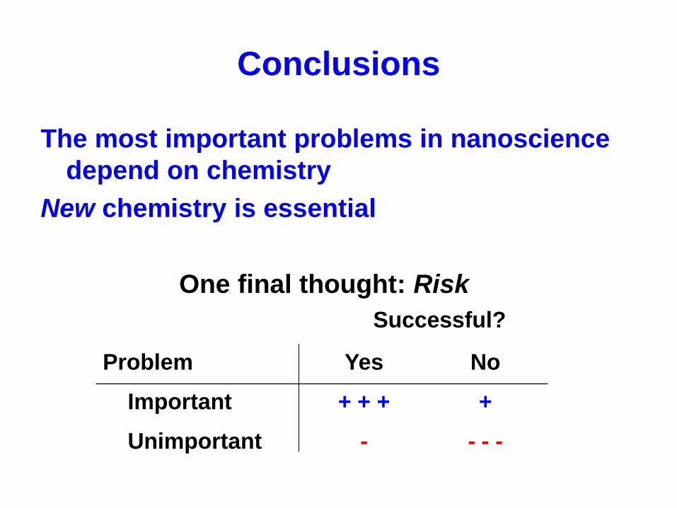
Conclusions
The most important problems in nanoscience depend on chemistry
New chemistry is essential One final thought: Risk
Problem Yes No
Important + + + +
Unimportant - - - -
Successful?

K. Aoki et al., Nature Materials 2 (2), 117 (2003)
[ B. H. Cumpston et al., Nature 398, 51 (1999) ]
Two-Photon Woodpile Crystal
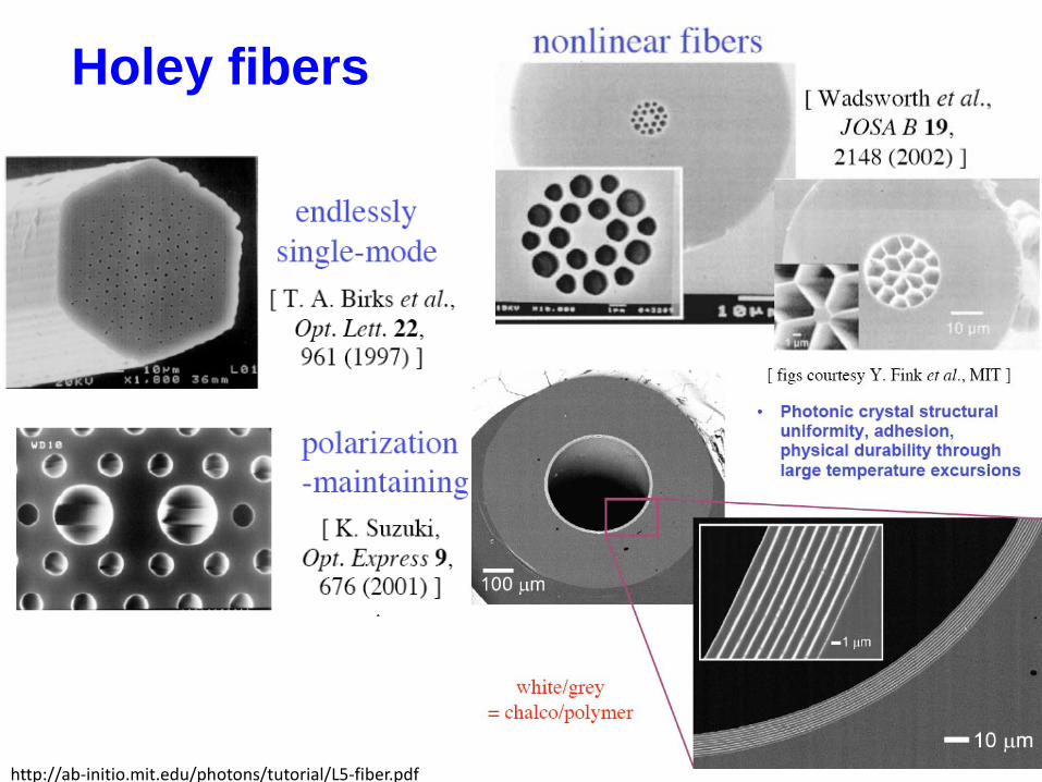
http://ab-initio.mit.edu/photons/tutorial/L5-fiber.pdf
Holey fibers
84
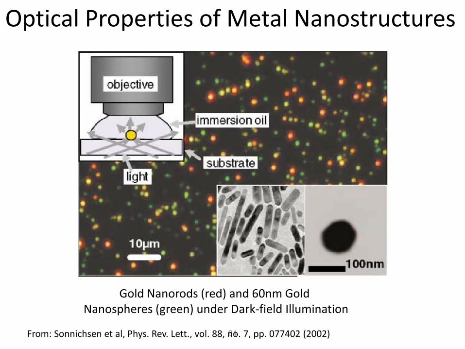
Optical Properties of Metal Nanostructures
From: Sonnichsen et al, Phys. Rev. Lett., vol. 88, no. 7, pp. 077402 (2002)
Gold Nanorods (red) and 60nm Gold Nanospheres (green) under Dark-field Illumination
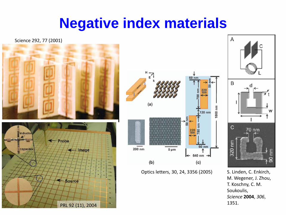
Negative index materials
Optics letters, 30, 24, 3356 (2005)
Science 292, 77 (2001)
PRL 92 (11), 2004
S. Linden, C. Enkirch, M. Wegener, J. Zhou, T. Koschny, C. M. Soukoulis, Science 2004, 306, 1351.

• Structure-reactivity relations
• Catalyst-support interactions
• Poisoning and Activation
• Stability
• Mass transport

Berkeley, CA: www.nrel.gov
Schatz Energy Research Center: www.humboldt.edu/~serc/animation.html
A stack of 36 PEM fuel cells
Plasma Display: http://www.de.nec.de/pressfiles/42vp4_plasma_display.jpg
Nanotechnology in Energy
Is it possible to design catalysts?
Tuning surface electronic structure of nanoparticle surface by alloying leads to improved reduction kinetics – Aided by surface science and nanoscience
new generation of oxygen reduction catalysts DFT calculated surface electronic structure
Alloying leads to reduction activity enhancements
Pt3M single crystal surfaces
Fundamental
Research…
…coupled with nanoscience leads to the design
of better O2 reduction catalysts
Pt3Co

Applications of Nanoskiving
Wiley et al. Nano Lett. 2008 Single-crystal nanowire plasmonic waveguides
Organic photovoltaic device
Conducting polymer nanowires
Lipomi et al. Adv. Funct. Mater. 2008
Lipomi et al. Nano Lett. 2008 Electrically addressable parallel nanowires Dickey et al. Nano Lett. 2008
Xu et al. Nano Lett. 2007 Frequency-selective surfaces
Xu et al. Nano Lett. 2007 Electrodes for electrodeposition

Templating • Example: electrochemical growth of core-shell and segmented metallic and polymeric tubes in anodic alumina membranes
Lahav et al. Nano Lett. 2006 C. Martin

Applications of Self-Assembled Particles
• Sensing — Chemi- and biosensors — Plasmonic rulers • Multifunctional carriers for delivery
• Data storage devices • Optoelectronic devices — Plasmon waveguides — Focusing lenses — Light generators — Optical switches • Nanoelectronics
Developing quickly
Developing slowly

Self-Assembly: Combining Top-down and Bottom-up
• Assembly in solutions – “artificial molecules” — Balance of attraction and repulsion forces — Molecular recognition
• Assembly using templating methods — Hard template: nanotubes, nanowires, nanofabricated templates — Soft template: synthetic polymers, proteins, DNA or viruses
• Assembly at interfaces — Langmuir-Blodgett technique — Sedimentation or evaporation-induced self-assembly — Adsorption of nanoparticles
• Assisted assembly of nanoparticles — Electric or magnetic fields — Shear forces — Light irradiation

SAMs
York et al. in prep
• Influence of defects in organic monolayers on growth of biofilms

Holey Fibers
http://ab-initio.mit.edu/photons/tutorial/L5-fiber.pdf
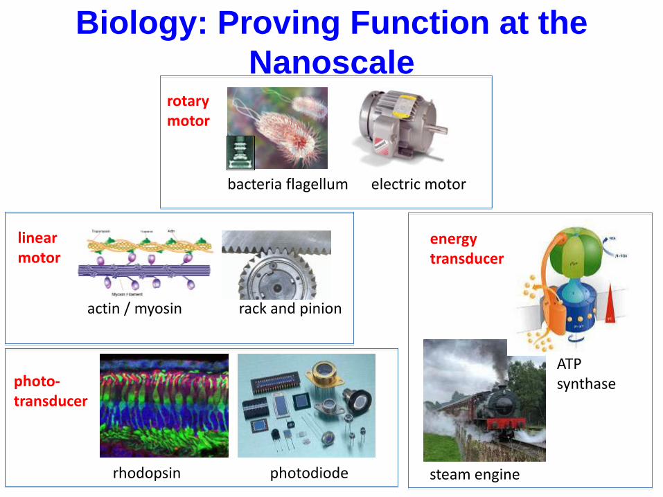
Biology: Proving Function at the Nanoscale
rotary motor
bacteria flagellum
linear motor
actin / myosin
electric motor
rack and pinion
rhodopsin
photo- transducer
photodiode
energy transducer
steam engine
ATP synthase

Particles for EM Heating
500 µm
Live cells, calcein-AM stain Dead cells, EthD-1 stain
In air, gold nanocages melted under camera flash as the temperature was raised by 200 degrees. In water, the temperature increase was enough to kill breast cancer cells targeted by gold nanocage at a laser (l=820 nm) power density of 0.9 W/cm2.
100 nm
Camera flash
Chen, Wang, Xi, Au, Siekkinen, Warsen, Li, Zhang, Xia & Li, Nano Lett. 2007

Nanoholes: DNA Sequencing
Nano Letters, 2008

Nanooptics
100 Sonnichsen et al, Phys. Rev. Lett., vol. 88, no. 7, pp. 077402 (2002)
Gold Nanorods (red) and 60nm Gold Nanospheres (green) under Dark-field Illumination
• Optical properties of metallic nanostructures

1 µm
The Cell