Nanometrology Device Standards for Scanning Probe ...
19
Portland State University Portland State University PDXScholar PDXScholar Physics Faculty Publications and Presentations Physics 1-6-2009 Nanometrology Device Standards for Scanning Nanometrology Device Standards for Scanning Probe Mmicroscopes and Processes for Their Probe Mmicroscopes and Processes for Their Fabrication and Use Fabrication and Use Peter Moeck Portland State University, [email protected] Follow this and additional works at: https://pdxscholar.library.pdx.edu/phy_fac Part of the Condensed Matter Physics Commons, and the Nanoscience and Nanotechnology Commons Let us know how access to this document benefits you. Citation Details Citation Details Moeck, Peter. "Nanometrology device standards for scanning probe microscopes and processes for their fabrication and use." U.S. Patent No. 7,472,576. 6 Jan. 2009. This Patent is brought to you for free and open access. It has been accepted for inclusion in Physics Faculty Publications and Presentations by an authorized administrator of PDXScholar. Please contact us if we can make this document more accessible: [email protected].
Transcript of Nanometrology Device Standards for Scanning Probe ...

Portland State University Portland State University
PDXScholar PDXScholar
Physics Faculty Publications and Presentations Physics
1-6-2009
Nanometrology Device Standards for Scanning Nanometrology Device Standards for Scanning
Probe Mmicroscopes and Processes for Their Probe Mmicroscopes and Processes for Their
Fabrication and Use Fabrication and Use
Peter Moeck Portland State University, [email protected]
Follow this and additional works at: https://pdxscholar.library.pdx.edu/phy_fac
Part of the Condensed Matter Physics Commons, and the Nanoscience and Nanotechnology
Commons
Let us know how access to this document benefits you.
Citation Details Citation Details Moeck, Peter. "Nanometrology device standards for scanning probe microscopes and processes for their fabrication and use." U.S. Patent No. 7,472,576. 6 Jan. 2009.
This Patent is brought to you for free and open access. It has been accepted for inclusion in Physics Faculty Publications and Presentations by an authorized administrator of PDXScholar. Please contact us if we can make this document more accessible: [email protected].

US007472576B1
(12) United States Patent (10) Patent N0.2 US 7,472,576 B1 Moeck (45) Date of Patent: Jan. 6, 2009
(54) NANOMETROLOGY DEVICE STANDARDS 4,687,987 A 8/1987 Kuchnir et a1. FOR SCANNING PROBE MICROSCOPES 4,966,952 A 10/1990 Riaza AND PROCESSES FOR THEIR FABRICATION 5,070,004 A 12/1991 Fujita et 31, AND USE 5,117,110 A 5/1992 Yasutake
5,194,161 A 3/1993 Heller et a1. (75) Inventor: Peter Moeck, Portland, OR (US) 5,223,409 A 6/1993 Ladner et a1‘
(73) Assignee: State of Oregon Acting By and 5347226 A 9/1994 Bachmann et a1’ . 5,403,484 A 4/1995 Ladner et a1.
Through The State Board of Higher 5 504 366 A 4/l996 Weiss et 31 Education On Behalf of Portland State ’ ’ '
University, Portland, OR (US)
( * ) Notice: Subject to any disclaimer, the term of this (Continued) patent is extended or adjusted under 35 USC 154(b) by 440 days' FOREIGN PATENT DOCUMENTS
(21) App1.No.: 11/282,395 CN 1209633 A 3/1999
(22) Filed: Nov. 17, 2005 (Continued)
Related US. Application Data _ _ _ _ OTHER PUBLICATIONS
(60) Prov1s1onal appl1cat1on No. 60/628,983, ?led on Nov. 17, 2004. Alchalabi et a1, “Self-assembled semiconductor quantum dots with
nearly uniform sizes,” Phys. Rev. Lett. 90:0261041-0261044 (Jan. (51) Int. C1. 2003)
B82B 1/00 2006.01 .
B82B 3/00 (2006.01) (Commued) G01B 21/00 (200601) Primary ExamineriThomas P Noland G01 N 13/10 (200601) (74) Attorney, Agent, or FirmiKlarquist Sparkman, LLP G12B 21/00 (2006.01)
(52) US. Cl. ............................ .. 73/1.75; 7/179; 7/189; (57) ABSTRACT 29/592; 977/701; 977/888
(58) Field of Classi?cation Search ................ .. 73/175, 73/179’ L89; 29/592’ DIG 105; 977/701’ Nanometrology device standards and methods for fabricating
977/888 and using such devices in conjunction With scanning probe See application ?le for Complete Search history microscopes are described. The fabrication methods com
prise: (1) epitaxial groWth that produces nanometer siZed (56) References Cited islands of knoWn morphology, structural, morphological and
Us‘ PATENT DOCUMENTS chemical stability in typical nanometrology environments, and large height-to-Width nano-island aspect ratios, and (2)
3,830,639 A 8/ 1974 Evans et a1, marking suitable crystallographic directions on the device for 4,100,091 A 7/ 1978 Powell alignment With a scanning direction.
4,267,507 A 5/1981 Guerpont 4,475,995 A 10/ 1984 Ziegler et a1. 17 Claims, 6 Drawing Sheets
1102 1700 1706
1704
US 7,472,576 B1 Page 2
US. PATENT DOCUMENTS 6,727,548 B1 4/2004 King 6,731,531 B1 5/2004 Forbesetal.
5,559,328 A 9/1996 Weiss eta1~ 6,746,517 B2 6/2004 Benson etal. 5,578,745 A 11/1996 Bayer et a1. 6,764,796 B2 7/2004 Fries 5,602,323 A 2/1997 Ohmi ....................... .. 73/179 6,768,918 B2 7/2004 Zelenchuk
5,605,800 A 2/1997 Kourilsky eta1~ 6,770,220 B1* 8/2004 Klimant ............... .. 252/301.36 5,619,035 A 4/1997 Weiss eta1~ 6,777,030 B2 8/2004 Veerasamyetal. 5,652,428 A 7/1997 Nishioka eta1~ 6,784,028 B2 8/2004 Rueckes et a1. 5665905 A 9/1997 Eartha eta1~ 6,870,309 B2* 3/2005 Blyablin et a1. ........... .. 313/310 5,729,015 A 3/1998 Tong ------------------------ -- 250/306 7,062,397 B1* 6/2006 Minor ....................... .. 702/90
5,760,901 A 6/1998 Hill 7,204,122 B2* 4/2007 Sullivan et a1. ............ .. 73/1.03 5,780,889 A 7/1998 Sethi 2001/0052122 A1 12/2001 Nanosetal. 5,825,670 A 10/1998 Chemoff er a1~ 2002/0025277 A1 2/2002 Dugas et a1. 5,830,287 A 11/1998 Pinnowetal 2002/0055033 A1 5/2002 Yadav etal. 5,837,500 A 11/1998 Ladner er 91- 2002/0113971 A1 8/2002 Zettleretal. 5,855,827 A V1999 Bussing eta1~ 2003/0062590 A1 4/2003 Anthony 5,876,928 A 3/1999 Kourilskyetal 2003/0080550 A1 5/2003 Phillips 5,905,000 A 5/1999 Yadav etal 2003/0132376 A1 7/2003 Bonnell et a1. 5936237 A 8/1999 Wm derweide 2003/0222050 A1 12/2003 Dugasetal. 5,948,972 A 9/1999 Samsavaretal 2004/0029041 A1 2/2004 Shih etal. 5,955,661 A 9/1999 samsavaretal' 2004/0037253 A1 2/2004 Bolandetal. 5,959,241 A 9/1999 stirametal 2004/0065252 A1 4/2004 Sreenivasan etal. 5,999,887 A 12/1999 Glannakopoulos eta1~ 2004/0120858 A1 6/2004 Dugasetal. 6,016,693 A V2000 Vianietal 2004/0146430 A1 7/2004 Dugas 6,028,008 A 2/2000 Bayer eta1~ 2005/0010310 A1* 1/2005 Touzov ...................... .. 700/56 6,060,549 A 5/2000 Li et a1. 6,066,806 A 5/2000 Higashiura et a1. .... .. 174/110 R FOREIGN PATENT DOCUMENTS 6,091,496 A 7/2000 Hill 6,146,390 A 11/2000 Heilbrun et a1. CN 1409109 A 4/2003 6,165,181 A 12/2000 Heilbrun et a1. CN 1434461 A 8/2003 6,214,368 B1 4/2001 Lee etal. (3N 1440087 A 9/2003 6,230,572 B1 5/2001 Pui et a1. CN 1440782 A 9/2003 6,237,029 B1 5/2001 Master et a1. (3N 1470322 A 1/2004 6,267,005 B1 7/2001 SaIIlSaVaI etal. DE 19651029 A1 6/1998 6,278,113 B1 8/2001 Murayama et a1. EP 0957333 A1 11/1999 6,337,215 B1 1/2002 Wilson EP 0736746 B1 3/2000 6,354,133 B1 3/2002 Yeduretal. EP 0676614 A1 6/2001 6,358,860 B1 3/2002 soheei et a1. EP 1251562 A1 10/2002 6,374,135 B1 4/2002 Bucholz EP 1298727 A2 4/2003 6,381,744 B2 4/2002 Nanosetal. JP 55155454 A2 12/1980 6,387,560 B1 5/2002 Yadav et 31‘ JP 59057110 A 4/1984 ............... .. 73/179 6,398,940 B1 6/2002 Chiet 31‘ JP 59057111 A 4/1984 ............... .. 73/179
6,405,583 B1 6/2002 Shirakawabe etal. JP 03122514 A2 5/1991 6,418,460 B1 7/2002 Bitar et a1. JP 05018708 A2 V1993 6,434,687 B1 8/2002 Huppenthal JP 05164512 A2 6/1993 6,459,482 B1 10/2002 Singh et a1. ............ .. 356/243.1 JP 05223704 A2 8/1993 6,463,319 B1 10/2002 Bucholz JP 05312506 A2 11/1993 6,480,285 B1 11/2002 Hill JP 06066512 A2 3/1994 6,490,913 B1 12/2002 Martin et a1. JP 06117844 A2 4/1994 6,491,702 B2 12/2002 Heilbrun et a1. JP 06201372 A2 7/1994 6,504,172 B2 1/2003 Zagoskin etal. JP 06201374 A2 7/1994 6,520,005 B2 2/2003 McWaid et a1. JP 07083650 A2 3/1995 6,537,847 B2 3/2003 Zagoskin etal. JP 07248332 A2 9/1995 6,544,698 B1 4/2003 Fries JP 08005313 A2 V1996 6,573,039 B1 6/2003 Dunlay etal. JP 08087701 A2 4/1996 6,573,497 B1 6/2003 Rangarajan et a1. JP 08233836 A2 9/1996 6,573,498 B1 6/2003 Rangarajan et a1. JP 08262037 A2 10/1996 6,589,229 B1 7/2003 Connelly etal. JP 08278315 A2 10/1996 6,591,658 B1 7/2003 Yeduretal. JP 09145722 A2 6/1997 6,610,355 B2 8/2003 Yadav etal. JP 11094862 A2 4/1999 6,611,039 B2 8/2003 Anthony JP 11304822 A2 11/1999 6,616,895 B2 9/2003 Dugasetal. JP 2002122529 A2 4/2002 6,620,591 B1 9/2003 Dunlay etal. JP 2002323429 A2 11/2002 6,635,874 B1 10/2003 Singh et a1. ............... .. 250/311 JP 2002350319 A2 12/2002 6,643,165 B2 11/2003 Segal et a1. JP 2003042928 A2 2/2003 6,643,616 B1 ll/2003 Granik et a1. JP 2003162954 A2 6/2003 6,661,004 B2 12/2003 Aumond et a1. JP 2004037325 A2 2/2004 6,689,650 B2 2/2004 Gambino etal. RU 2179704 (:2 2/2002 6,706,402 B2 3/2004 Rueckes et a1. W0 W09908785 A2 2/1999 6,709,018 B2 3/2004 Phillips W0 W09935600 A2 7/1999 6,720,553 B2 4/2004 Bonnell et a1. W0 W09946558 A1 9/1999 6,723,187 B2 4/2004 Segal et a1. W0 W00070297 A3 11/2000 6,727,071 B1 4/2004 Dunlay etal. W0 W00106227 A2 1/2001

US 7,472,576 B1 Page 3
WO WO0205304 1/2002 WO WO03019238 3/2003 WO WO03105184 12/2003 WO WO03107433 12/2003 WO WO2004035211 4/2004 WO WO04053860 6/2004 WO WO2004050237 6/2004 WO WO04055786 7/2004
OTHER PUBLICATIONS
Ferreira et al., “AFM characterization of PbTe quantum dots grown by molecular beam epitaxy under Volmer-Weber mode,” J'. Cryst. Growth 231: 121-128 (2001). Grif?th and Grigg, “Dimensional metrology with scanning probe microscopes,” J'. Appl. Phys. 74(9):R83-R109 (Nov. 1993). Keller and Franke, “Envelope reconstruction of probe microscope images,” Surface Science 294:409-419 (May 1993). Luders et al., “Self-organized structures in CoCr2O4 (001) thin ?lms: Tunable growth from pyramidal clusters to a {111} fully faceted surface,” Phys. Rev. B 70:045403.1-045403.6 (Jul. 2004). PincZolits et al., “Direct formation of self-assembled quantum dots under tensile strain by heteroepitaxy of PbSe on PbTe (111),” Appl. Phys. Lett. 73(2):250-252 (Jul. 1998). PincZolits et al., “Molecular beam epitaxy of highly faceted self assembled IV-VI quantum dots with biomodal siZe distribution,” J'. Cryst. Growth 201/202: 1126-1 130 (1999).
Raab et al., “Atomic Force Microscopy and Transmission Electron Microscopy Study of Self-Organized Ordering in Vertically Aligned PbSe Quantum Dot Superlattices,” Mat. Res. Symp. Proc. 696:N7.2. 1-N7.2.6 (2002). SpringholZ et al., “Dot siZe dependence of vertical and lateral order ing in self-organized PbSe/Pb1_XEuXTe quantum-dot superlattices,” App. Phys. Lett. 82:799-801 (Feb. 2003). SpringholZ et al., “Self-Organized Growth of Three Dimensional Quantum-Dot Crystals with fcc-Like Stacking and a Tunable Lattice Constant,” Science 282:734-737 (Oct. 1998). SpringholZ et al., “Tuning of Vertical and Lateral Correlations in Self-Organized PbSe/ Pb l_XEuXTe Quantum Dot Superlattices,” Phys. Rev. Lett. 84:4669-4672 (May 2000). SpringholZ et al., Self-organized ordering in self-assembled quantum dot superlattices, Materials Science and Engineering 88: 143-152 (2002). Stangl et al., “Structural properties of self-organized semiconductor nanostructures,” Rev. Mod. Phys. 76:725-783 (Jul. 2004). SpringholZ et al., “Controlling of lateral and vertical order in self organiZed PbSe quantum dot superlattices,” Proc. 25th Int. Conf on the Physics of Semiconductors, Sep. 2000, Osaka, Japan, Miura and Ando, eds. (Springer 2001), p. 355-358. Wang et al., “Size, shape, and stability of InAs quantum dots on the GaAs(001) substrate,” Physical Review B 62: 1897-1904 (Jul. 2000).
* cited by examiner
US. Patent Jan. 6, 2009 Sheet 1 of6 US 7,472,576 B1

US. Patent Jan. 6, 2009 Sheet 2 of6 US 7,472,576 B1
FIG. 4
FIG. 5 STEP HEIGHT --—
20-25 nm i1 nm

US. Patent Jan. 6, 2009 Sheet 3 of6 US 7,472,576 B1
FIG. 7
FIG. 8
FIG. 9

US. Patent Jan. 6, 2009 Sheet 4 of6 US 7,472,576 B1
US. Patent
FIG. 13
FIG. 14
Jan. 6, 2009 Sheet 5 0f 6 US 7,472,576 B1
1308 PbSe
CaF2 1302
(11])Si J
1402
CoCrO4
001 MgAl2O4 J1404

US. Patent Jan. 6, 2009 Sheet 6 0f6 US 7,472,576 B1
PbSe 1502 FIG. 15 PbTe J
1504 (111) BaFz J
1608 1606 \i K“ 'IIIIIIIIIII/IIII/IIIIIIIIIIIIIIIIIIIIIIIIA
Q
FIG. 16 °

US 7,472,576 B1 1
NANOMETROLOGY DEVICE STANDARDS FOR SCANNING PROBE MICROSCOPES
AND PROCESSES FOR THEIR FABRICATION AND USE
CROSS REFERENCE TO RELATED APPLICATIONS
This application claims the bene?t of US. Provisional Application 60/628,983, ?led Nov. 17, 2004 and that is incor porated herein by reference.
FIELD
The disclosure pertains to nanometrology device stan dards.
BACKGROUND AND SUMMARY
With the advent of science and engineering on the nanom eter scale, scanning probe microscopes are increasingly used for nanometrology applications. Scanning probe micro scopes use various probe tip con?gurations for assessing a range of physical properties on the atomic and nanometer scale. Based on the physical detection principle, a scanning probe microscope can be referred to as a scanning tunneling microscope, an atomic force microscope, a magnetic force microscope, or other type of microscope. The availability of these various con?gurations has permitted a wide range of nanometer scale measurements.
One particular application of scanning probe microscopy is in the measurement and characterization of specimen topog raphy. HoWever, accurate specimen metrology requires dimensional standards and standardized procedures for cali bration. An absolute length reference is typically unavailable on a sample of interest, and nanometrology device standards are needed. Conventional “top-doWn” approaches for fabri cating length references are based on conventional semicon ductor manufacturing lithographic and etching processes. HoWever, these processes are suitable for reference standards having feature heights greater than about 20 nm and feature pitches greater than about 1 pm, and smaller feature siZes are unavailable.
In many applications, interactions of a scanning probe tip and a sample are complex, and measurements of sample topography are complicated by the ?nite siZe of the scanning probe tip. See, for example, I. G. Gri?ith and D. A. Grigg, “Dimensional metrology With scanning probe microscopes,” J. Appl. Phys. 74, R83 (1993) and D. J. Keller and F. S. Franke, “Envelope reconstruction of probe microscope images,” Surface Science 294, 409 (1993). Accurate micro scope calibration could permit deconvolution of the effects of ?nite probe tip siZe from specimen measurements.
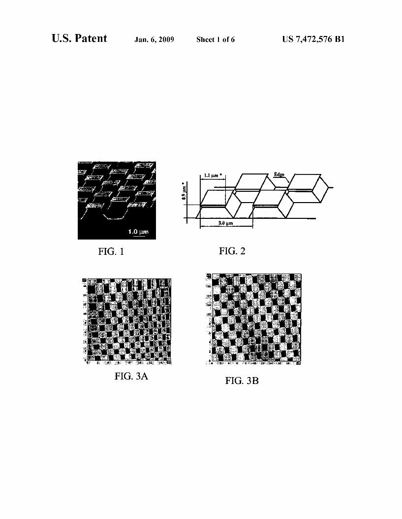
FIGS. 1, 2, and 3A-3B illustrate a typical lithographically produced nanometrology device standard and microscope calibration based on such a device standard. Using such a device, a microscope canbe calibrated for lateral dimensional measurements, and lateral non-linearity, hysteresis, creep, and cross-coupling effects can be identi?ed and compen sated. FIGS. 1-2 illustrate a conventional silicon calibration grating that includes a chessboard-like array of square pillars With sharp undercut edges formed by (110) planes of silicon. Step heights are on the order of 1 um and the pitch is on the order of a feW um, Wherein the pitch is generally accurate to Within 17.5 nm. The edge curvature is less than 5 nm. FIGS. 3A-3B illustrate scanning probe microscopy images before
20
25
30
35
40
45
50
55
60
65
2 and after lateral scan nonlinearities are corrected, respec tively, based on a nanometrology standard such as that illus trated in FIGS. 1-2.
FIGS. 4-5 illustrate a conventional “top-doWn” nanome trology standard for vertical calibrations. This standard includes a quasi-one-dimensional array of rectangular SiO2 steps that are 20 to 25 nm high and that are formed on a silicon Wafer. The area of this standard is about 9 m2. Step height is typically accurate to about :1 nm. The array is generally coated With Si3N4 to prevent Si from oxidation. Vertical cali bration and linearity corrections are typically based on sev eral such devices With different nominal step heights such as, for example, 22.5 nm, 100 nm, 500 nm, 1000 nm, and 1500 nm.
Since scanning tunneling microscopes (and special atomic force microscopes that operate in vacuum) can have resolu tion on an atomic scale, reference samples of inorganic crys talline materials having knoWn lattice constants can be used as lateral calibration standards. For example, highly ordered pyrolytic graphite can be used. In a [0001] oriented graphite crystal, the lateral lattice constant, ie the length of the <1000> and <1100> lattice vectors can be measured directly and is knoWn to be 0.2462 nm. A single atomic monolayer step of graphite is knoWn to be 0.3354 nm high. Thus, mul tilayer steps must have heights that are integral multiples of this monolayer step height. Such single- and multilayer steps can be used for vertical calibrations of scanning probe micro scopes. Standards based on other inorganic crystals can also be used to obtain lateral and vertical calibrations of less than about 1 nm. For example, a Si (1 1 1) surface such as illustrated in FIG. 6 can be used. This surface has a lateral period of 2.688 nm.
Thus, nanometrology device standards canbe obtained that are suitable for calibrations from atomic dimensions up to a feW nm. There is, hoWever, a gap betWeen these atomic pre cision nanometrology device standards and the about 20 nm dimensions of nanometrology device standards that are pro duced by the top-doWn approach. Accordingly, improved device standards and methods are needed.
SUMMARY
According to representative examples, calibration stan dards comprise a substrate and at least one nano-island situ ated at a surface of the substrate. An indicia associated With a crystallographic orientation of the at least one nano-island is ?xed With respect to the nano-island. In some examples, the indicia is situated on the substrate or at the at least one crystal island. In additional examples, the calibration standards com prise a plurality of nano-islands. The indicia canbe associated With a cleavage plane of the substrate or the nano-island. In representative embodiments, the substrate is (111) oriented silicon or (111) oriented BaF2, and a buffer, stress relief, or other layer is situated betWeen the substrate and the at least one nano-island. In typical examples, the nano-island has dimensions of betWeen about 2 nm and 20 nm.
Methods of fabricating a calibration standard comprise forming at least one nano-island at a surface of a substrate and providing an indicia of a crystallographic orientation of the nano-island, Wherein the indicia is ?xed With respect to the nano-island. In some examples, the indicia is provided by cleaving at least one of the substrate and the nano-island. In other examples, the indicia is based on X-ray diffraction analysis of the nano-island or is based on electron backscatter diffraction. In representative examples, the at least one nano island is formed by epitaxial groWth and has dimensions of
US 7,472,576 B1 3
between about 2 nm and 10 nm. In further examples, a plu rality of nano-islands is formed at the surface of the substrate.
Methods comprise evaluating a nano-island With a scan ning probe microscope, and calibrating the scanning probe microscope based on the evaluation. In representative examples, the calibration is associated With compensation of a scan nonlinearity. In additional examples, methods further comprise selecting a hardness of the nano-island based on a scanning probe hardness and evaluating a plurality of nano islands of at least tWo different heights With the scanning probe microscope, Wherein the scanning probe microscope is calibrated based on the evaluation.
The foregoing and other objects, features, and advantages of the technology Will become more apparent from the fol loWing detailed description, Which proceeds With reference to the accompanying ?gures.
BRIEF DESCRIPTION OF THE DRAWINGS
FIG. 1 is a scanning electron microscopy image of a con ventional nanometrology device standard.
FIG. 2 is a representation of a conventional nanometrology device standard. Dimensions noted With asterisks are given for information only and are not intended to serve as stan dards.
FIGS. 3A-3B are scanning probe microscopy images of the nanometrology device standard of FIG. 1 before (FIG. 3A) and after (FIG. 3B) correction of lateral nonlinearity. The images correspond to an area of about 400 umz.
FIG. 4 is a scanning electron microscopy image of a con ventional nanometrology device standard.
FIG. 5 is a schematic diagram of a conventional nanome trology device standard. Dimensions noted With an asterisk are listed for information only, and are do not generally serve as reference standards.
FIG. 6A is a tWo dimensional scanning tunneling micros copy image of a reconstructed surface of (111) oriented sili con. Image area is about 4900 nm2.
FIG. 6B is a schematic diagram illustrating an atomic arrangement of reconstructed (111) oriented silicon such as shoWn in FIG. 6A.
FIG. 7 is a 3D atomic force microscopy image of PbSe nano-islands on (111) oriented PbTe for nanometrology (modi?ed after M. PincZolits et al., J. Cryst. GroWth 201-202, 1126 (1999)). The height of the larger nano-islands (type A) is approximately 16.5 nm, and the height of the tWo smaller nano-islands (type B) is about 10 nm. The shape of all three nano-islands is that of trigonal pyramids With {100} facets. The nano-island aspect ratio (height to half-base Width in the
[-1-12], [-12-1], and [2-1-1] directions) is approximately The corresponding angle betWeen the (111) surface normal
and the (100), (010) and (001) facets is approximately 57.74°. The angle betWeen the [2-1-1] and the [100] direction is approximately 35.26°. The total nano-island density is approximately 100 um”.
FIG. 8 is a 3D atomic force microscopy image of PbSe nano-islands on (111) oriented PbTe (modi?ed after Pinc Zolits et al., Appl. Phys. Lett. 73, 250 (1998)). The nano island height is approximately 16.5 nm, the shape is that of trigonal pyramids With {100} facets. The nano-island aspect ratio (height to half-base Width in the [-1-12], [-12-1], and [2-1-1] directions) is approximately Nano-island density is approximately 100 um‘?
FIG. 9 is a 3D atomic force microscopy image of PbSe nano-islands on (111) oriented PbTe (after Alchalabi et al., Phys. Rev. Lett. 90, 26104 (2003)). Nano-island height is approximately 19 nm, and nano-island shape is that of trigo
20
25
30
35
40
45
50
55
60
65
4 nal pyramids With {100} facets. Nano-island aspect ratio (height to half-base Width in the [-1-12], [-12-1] and [2-1-1] directions) is approximately/ 2. Nano-island density is approximately 120 um“?
FIGS. 10A-10B are 2D atomic force microscopy images of a single PbSe nano-island layer (FIG. 10A) and of a last layer of a sixty-period PbSe/(Pb,Eu)Te superlattice on (111) ori ented PbTe (FIG. 10B), respectively. The ?gure inserts shoW 2D poWer spectra of the atomic force microscopy images that indicate the hexagonal ordering of the dots of FIG. 10B. Nano-island density is approximately 170 pm“2 for the single PbSe layer, and approximately 295 pm‘2 for the top PbSe layer of the sixty-period PbSe/(Pb,Eu)Te superlattice.
FIG. 11 is a scanning electron microscopy image of CoCr2O4 islands on (001) oriented MgAl2O4 (after Liiders, et al., Phys. Rev. B 70, 45403 (2004)). The island siZe distribu tion is bimodal, With nano-islands having heights smaller than about 50 nm and micro-islands having heights as great as about 500 nm. The shape of the nano-islands is that of tet ragonal pyramids With {111} facets so that there is a nano island aspect ratio (height to half-base Width in the [110], [1 -10], [-1-10], and [-110] directions) of approximately \/2. The combined nano-island density is approximately 5 pm‘?
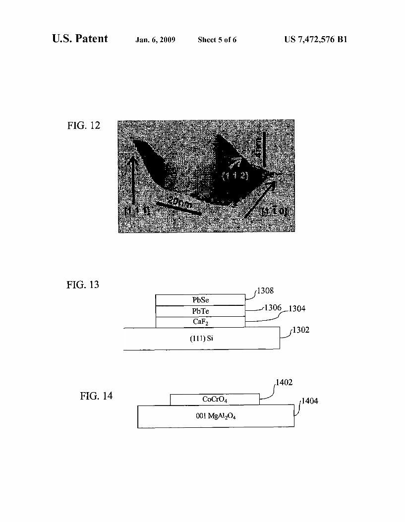
FIG. 12 is a 3D atomic force microscopy image of a single PbTe nano-island on (1 1 1) oriented BaF2 (after Ferreira et al., J. Cryst. GroWth 231, 121 (2001)). Nano-island height is approximately 4 nm. Nano-island shape is that of trigonal pyramids With {211} facets so that there is a nano-island aspect ratio (height to half-base Width in the [-1-12], [-12-1], and [2-1-1] directions) of approximately 0.3 536. Nano-island density is approximately 120 um“?
FIGS. 13-16 are schematic diagrams of representative nano-island metrology standards.
FIG. 17 is a perspective vieW of a representative nano island metrology standard.
DETAILED DESCRIPTION
As used in this application and in the claims, the singular forms “a,” “an,” and “the” include the plural forms unless the context clearly dictates otherWise. Additionally, the term “includes” means “comprises.” Further, the term “coupled” means electrically or electromagnetically connected or linked and does not exclude the presence of intermediate elements betWeen the coupled items.
Disclosed beloW are representative embodiments of metrology standards and associated methods of fabrication and use. The described systems, apparatus, and methods should not be construed as limiting in any Way. Instead, the present disclosure is directed toWard all novel and nonobvi ous features and aspects of the various disclosed embodi ments, alone and in various combinations and sub-combina tions With one another. The disclosed systems, methods, and apparatus are not limited to any speci?c aspect or feature or combinations thereof, nor do the disclosed systems, methods, and apparatus require that any one or more speci?c advan tages be present or problems be solved.
Although the operations of some of the disclosed methods are described in a particular, sequential order for convenient presentation, it should be understood that this manner of description encompasses rearrangement, unless a particular ordering is required by speci?c language set forth beloW. For example, operations described sequentially may in some cases be rearranged or performed concurrently. Moreover, for the sake of simplicity, the attached ?gures may not shoW the various Ways in Which the disclosed systems, methods, and apparatus can be used in conjunction With other systems,

US 7,472,576 B1 5
methods, and apparatus. Additionally, the description some times uses terms like “produce” and “provide” to describe the disclosed methods. These terms are high-level abstractions of the actual operations that are performed. The actual opera tions that correspond to these terms Will vary depending on the particular implementation and are readily discernible by one of ordinary skill in the art.
Disclosed herein are standards and associated methods of fabrication and use based on a “bottom-up” approach. Natu rally occurring self-assembly and ordering processes can be used to produce Well de?ned structures that have knoWn feature siZes and morphologies of nm siZe in three dimen sions. Epitaxial self-assembly of nanometer siZed islands, referred to herein as nano-islands, can produce suitable nanometrology device standards. Self assembly of nano-is lands is described in Alchalabi et al., “Self-assembled semi conductor quantum dots With nearly uniform siZes,” Phys. Rev. Lett. 90, 26104 (2003), Ferreira et al., “AFM character iZation of PbTe quantum dots groWn by molecular beam epitaxy under Volmer-Weber mode,” J. Cryst. GroWth 231, 121 (2001), Liiders et al., “Self-organized structures in CoCr2O4 (001) thin ?lms: Tunable groWth from pyramidal clusters to a {111} fully faceted surface,” Phys. Rev. B 70, 45403 (2004), PincZolits et al., “Direct formation of self assembled quantum dots under tensile strain by heteroepitaxy of PbSe on PbTe (111),” Appl. Phys. Lett. 73, 250 (1998), Raab et al., “Atomic Force Microscopy and Transmission Electron Microscopy Study of Self-OrganiZed Ordering in Vertically Aligned PbSe Quantum Dot Superlattices,” Mat. Res. Symp. Proc. Vol. 696, N7.2.1 (2002), PincZolits et al., “Molecular beam epitaxy of highly faceted self-assembled IV-VI quantum dots With bimodal size distribution,” J. Cryst. GroWth 201-202, 1126 (1999), SpringholZ et al., “Self-Orga niZed GroWth of Three-Dimensional Quantum-Dot Crystals With fcc-Like Stacking and a Tunable Lattice Constant,” Sci ence 76, 1675 (1996), SpringholZ et al., “Tuning ofVertical and Lateral Correlations in Self-OrganiZed Pb Se/ Pb l_,€Eu,€Te Quantum Dot Superlattices,” Phys. Rev. Lett. 84, 4669 (2000), SpringholZ et al., “Controlling of lateral and vertical order in self-organiZed PbSe quantum dot superlattices,” Proc. 25th Int. Conf. on the Physics of Semiconductors, Sep tember 2000, Osaka, Japan, Miura and Ando, eds. (Springer 2001), p. 355-358, SpringholZ et al., Self-organiZed ordering in self-assembled quantum dot superlattices,” Materials Sci ence and Engineering B 88, 143-152 (2002), SpringholZ et al., “Dot siZe dependence of vertical and lateral ordering in self-organiZed PbSe/Pbl_xEuxTe quantum-dot superlattices,” App. Phys. Lett. 82, 799 (2003), and Stangl et al., “Structural properties of self-organiZed semiconductor nanostructures,” Rev. Mod. Phys. 76, 725 (2004).
Nano-islands have several characteristics that make them particularly suitable for metrological standards. Nano-island morphology is knoWn, stable, and uniform so that sample topography/scanning tip deconvolutions can be calculated. Nano-islands have structural, morphological, and chemical stability in typical nanometrology laboratory environments. Nano-islands have morphological uniformity that is largely independent of nano-island height since the nano-island fac ets are the crystallographic net-planes With the loWest or a very loW surface energy (except for very small heights). In addition, nano-islands have large height-to-Width aspect ratios so that elastic lattice mismatch strain resulting from the heteroepitaxial groWth in the Stranski-KrastanoW or Volmer Weber mode tends to be partly relieved. Nano-islands can be produced With Wide or narroW siZe distributions, and Within hardness ranges that alloW calibrations With scanning tips of different hardnesses. In order to use nano-islands as calibra
20
25
30
35
40
45
50
55
60
65
6 tion standards, indicia that are detectable either macroscopi cally or microscopically can be provided to indicate crystal lographic alignment of the nano-islands With respect to, for example, a scanning direction of a scanning probe micro scope. In addition, aspect ratios, dimensions, siZe distribu tions, or other characteristics can be provided.
Application of nanometrology device standards to scan ning probe microscopy can be achieved by calibrating, cor recting, and ?ne tuning the scanning probe micro scope With a nanometrology device standard until a measurement of the standard yields a value or values identical or suf?ciently close to the dimensions or other values that are certi?ed for the standard. In some examples, nanometrology device standards described herein are associated With ?xed angles betWeen a sample surface and nano-island facets, and these angles can be used for calibration.
Representative examples of nanometrology device stan dards for scanning probe microscopes, processes for the fab rication of such standards, and use of the standards are described. Generally speaking, the representative standards consist of epitaxial structures With nano-islands that possess either three symmetrically equivalent {100} facets on a (11 1) oriented substrate (referred to herein as “type 1”), four sym metrically equivalent {111} facets on a (001) oriented sub strate (“type 2”), or three symmetrically equivalent {112} facets on a (111) oriented substrate (“type 3”). In all cases, there can also be tiny top facets more or less parallel to the surface normals of the substrate, a variety of free surface reconstructions or a slight rounding of the intersection points ofthe above mentioned {100}, {111}, and {112} facets. The nano-islands are of single crystalline materials and are chemi cally, structurally, and morphologically stable. Nano-islands that are of a material that occurs naturally as a mineral Will also generally be stable in the nano-metrology laboratory environment. One suitable process for nanometrology device standard
fabrication is heteroepitaxial self-assembly in either the Stranski-KrastanoW or the Volmer-Weber groWth mode com bined With processes that indicate the relevant crystallo graphic directions of the nano-islands. Such indications can be con?gured to be visible either macroscopically or micro scopically. Crystallographic orientations can be revealed by, for example, partial or complete cleaving of (111) oriented substrates having rock salt or diamond structure. Altema tively, standard X-ray crystallographic or electron backscat tering diffraction identi?cation and marking of loW-indexed crystallographic directions that are perpendicular to the sur face normal can be used With substrates having the spinel structure or other structures that do not cleave Well.
Substrates that are particularly suitable for nano-island self assembly include (111) (type 1 and 3) or (001) (type 2) oriented single crystals of the cubic crystal system having, for example, diamond, rock salt, or spinel structure. While cubic nano-islands on (111) oriented substrates tend to have three symmetrically equivalent {100} (type 1) or three symmetri cally equivalent {112} facets (type 3), their counterparts on (001) oriented substrates have four symmetrically equivalent {111} facets (type 2). Type 1 nano-islands can be groWn in the Stranski-Krast
anoW groWth mode to produce representative nano-islands as shoWn in FIGS. 7-10. Such nano-islands have nano-island aspect ratios (i.e., height to half-base Width ratio in the three symmetrically equivalent [2-1-1], [-12-1] and [-1-12] direc tions) of approximately \/2. The height to the full-base Width ratio for type 1 nano-islands is approximately \/2/3 or about 0.4714. These high-aspect ratio nano-islands exhibit their facetted equilibrium form for all but the smallest island

US 7,472,576 B1 7
heights. The rather high aspect ratio of these islands results from the 54.736o angle between {1 11} and {100} planes, and tends to provide relief of elastic mismatch strain energy due to relaxation of the crystal lattice of the upper part of the nano islands. These nano-island are thus thermodynamically (structurally, chemically, and morphologically) stable at all but the smallest heights in typical laboratory environments and can have either a narroW siZe distribution (Within approxi mately 2-25%) or a broad siZe distribution.
Type 2 nano-islands such as shoWn in FIG. 11 have a nano-island aspect ratio (i.e. height to half-base Width ratio in the four symmetrically equivalent [110], [1-10], [-1-10], and [-110] directions) of approximately \/2. The height to the full-base Width ratio is approximately 72-1 for type 2 nano islands, or roughly 0.7071. These high-aspect ratio nano islands possess their facetted equilibrium form for all but the smallest island heights. The extremely high aspect ratio of these nano-islands results from the 54.736o angle betWeen {100} and {111} planes, and ensures that there is relief of elastic mismatch strain energy due to relaxation of the crystal lattice of the upper part of the nano-islands. Such nano islands are thus thermodynamically stable at all but the small est island heights in a typical nanometrology laboratory envi ronments. Generally, such nano-islands can be formed With a broad distribution of siZes.
Type 3 nano-islands such as shoWn in FIG. 12 exhibit a nano-island aspect ratio (i.e. height to half-base Width ratio in the three symmetrically equivalent [2-1-1], [-12-1], and [-1 12] directions) of approximately arccos(2/\/5~ \/3)z0.3536. The height to full-base Width ratio is approximately 0.1179 for type 3 nano-islands. The relatively high aspect ratio of these nano-islands result from the 19.471 0 angle between {1 11} and {1 12} planes, and ensures that there is a suf?cient relief of elastic mismatch strain energy due to relaxation of the crystal lattice of the upper part of the nano-islands for the {112} planes to be stable. These nano-island are thus ther modynamically stable at all but the smallest island heights in typical nanometrology laboratory environments.
Type 1, 2 and 3 nanometrology device standards can be used in calibration of scanning probe microscopes. Typical number densities of nano-islands are in a range of from 1 to 500 pm‘? These number densities can generally be selected to provide spacing betWeen nano-islands so that height mea surements (Z-coordinates) based on a particular nano-island are substantially independent of adj acent nano-islands. Typi cal nano-island heights are in a range of from about 1 nm to 500 nm. Height measurements in scanning probe micro scopes are intrinsically more sensitive thanx- and y-measure ments and can be calibrated by standards With a certi?ed roughness. Over the knoWn large nano-island aspect ratios and height to full-base Width ratios, this height sensitivity can be used for the calibration of lateral measurements.
Since the shapes of type 1, 2 and 3 nano-islands are knoWn, scanning tip shape/nano-island shape deconvolutions can be calculated to determine the shape of a scanning probe tip. With the shape of the scanning probe tip determined in this Way, deconvolutions of the ?nite probe tip siZe from measure ments of nanometer- siZed objects of interest can be calculated in order to better estimate actual object shapes and siZes. Using nanometrology device standards that feature laterally ordered arrays of nano-islands such as illustrated in FIG. 10B, further calibrations of scanning probe microscopes such as, for example, the removal of non-linearities in x- and y-scan ning, can be achieved. In summary, very accurate calibrations of scanning probe microscopes can be achieved With the help of the above described type 1, 2, and 3 nanometrology device standards.
20
25
30
35
40
45
50
55
60
65
8 In order to provide such nanometrology standards, particu
larly those that can ?ll the gap betWeen the atomic precision nanometrology standards that alloW calibrations up to a feW nm, and conventional “top doWn” nanometrology device standards that alloW calibrations doWn to about 20 nm, so called “bottom-up approaches” are described. These “bottom up” approaches can be used to provide standards suitable for a Wide range of dimensions but are particularly needed for dimensional calibrations for Which atomic precision stan dards are too small, and “top doWn” standards are too large. Representative examples of such standards are described beloW.
Epitaxial self-assembly of PbSe (clausthalite) or Pb(Se,Te) With high PbSe content islands on PbTe (altaite) in the Stran ski-KrastanoW mode leads to nanometer siZed three-dimen sional islands that possess suitable properties for nanometrol ogy device standard applications. Epitaxial self-assembly of CoCr2O4 (cochromite) islands on MgAl2O4 (spinel) sub strates produces nanometer siZed three-dimensional islands that also have suitable properties for nanometrology applica tions. Epitaxial self-assembly of PbTe (altaite) in the Volmer Weber mode produces nanometer siZed three-dimensional islands that also have suitable properties for nanometrology device standard applications.
Other epitaxial materials systems can also be used to pro duce nanometer siZed three-dimensional islands that have suitable properties for nanometrology device standard appli cations. While PbSe and PbTe possess a Mohs hardness of 2.5, CoCr2O4 is much harder, having a Mohs hardness of 7. All three types of nanometrology device standards can, thus, be used in different scanning probe modes and With scanning probe tips of different harnesses. The self-assembly of nano-islands is a result of the epi
taxial groWth mode. One of many examples of the ?rst type of the device is a Wafer of (1 1 1) oriented BaF2 (frankdicksonite) substrate on Which ?rstly a lattice matched Pb(Se,Te) buffer layer or a PbTe buffer layer and secondly either a PbSe or Pb(Se,Te) nano-island layer With high PbSe content are groWn epitaxially by means of molecular beam epitaxy or metal organic vapor phase epitaxy in the Stranski-KrastanoW mode. The ?nal PbSe or Pb(Se,Te) nano-island layer may be replaced by a strain symmetriZed superlattice of several PbSe or Pb(Se,Te) nano-island layers With high PbSe content sepa rated by (Pb,Eu)(Se,Te) spacer layers With a high PbTe con tent that ends in nano-islands. These multilayer superlattices can also be groWn epitaxially by the same methods. The process of the fabrication of this device comprises epitaxial groWth and the introduction of macroscopically or micro scopically visible edges parallel to <110> directions that are perpendicular to the Wafer normal by partial or total cleaving of the pseudo-substrate While taking advantage of the three naturally occurring {1 1 1 } cleavage planes that are inclined by 70.5290 to the (111) BaF2 plane.
For scanning probe microscope calibration, the nano-is lands of this nanometrology device standard are aligned With their <110> edges (the intersections of the nano-island facets With the BaF2 Wafer normal) perpendicular to the scanning direction. This is achieved by taking advantage of the mac roscopically or microscopically visible <110> direction markers. When the scanning probe tip scans over such a nano-island, it folloWs a [2-1-1], [1-21] or [11-2] direction. First the scanning probe tip goes up a nano-island (100), (010), or (001) plane. Each of these planes makes an angle of 54.7360 With the (111) surface normal. Then the scanning probe tip goes doWn a nano-island [-100], [0-10], or [00-1] edge. Each of these edges makes an angle of 32.2640 With the (111) surface normal. The three-fold symmetry of the nano

US 7,472,576 B1
island is taken advantage of for the microscope calibration by adjusting each one of the above mentioned <110> directions to be perpendicular to the scanning direction, one after the other, repeating the calibration procedure three times, and averaging the results.
Another of many examples of the ?rst type of the device is a Wafer of (1 1 1) oriented Si substrate on Which ?rstly a CaF2 (?uorite) buffer layer, secondly a BaF2 buffer layer, thirdly a lattice matched Pb(Se,Te) buffer layer or a PbTe buffer layer, and fourthly either a PbSe or Pb(Se,Te) nano-island layer With high PbSe content or a strain symmetriZed superlattice of several PbSe or Pb(Se,Te) nano-island layers With high PbSe content separated by (Pb,Eu)(Se,Te) spacer layers With a high PbTe content are groWn epitaxially by molecular beam epitaxy or metal organic vapor phase epitaxy. The fabrication of this device comprises epitaxial groWth and the introduction of macroscopically or microscopically visible edges parallel to <1 12> directions that are perpendicular to the Wafer normal by either partial or complete cleavage of the pseudo-substrate While taking advantage of the three naturally occurring { 1 10} cleavage planes that are inclined by 90° to the (1 1 1) nanome trology device surface.
For microscope calibration, the nano-islands of this nanometrology device standard are aligned With their <110> edges (the intersections of the nano-island facets With the Si Wafer normal) perpendicular to the scanning direction. This is achieved by taking advantage of the macroscopically or microscopically visible <112> directions. The three-fold symmetry of the nano-island is taken advantage of by adjust ing each of the above mentioned <110> directions to be perpendicular to the scanning probe direction, one after another, repeating the calibration procedure three times, and averaging the results. One of many examples of the second type of the device is
a Wafer of (100) oriented MgAl2O4 (spinel) on Which CoCr2O4 (cochromite) nano-islands are groWn epitaxially by radio -frequency magnetron sputtering. The fabrication of this device comprises epitaxial groWth and the introduction of macroscopically or microscopically visible markers parallel to <1 10> directions that are perpendicular to the Wafer normal by employing standard X-ray crystallographic or electron backscatter diffraction determination of these directions and their marking by suitable processes. Another of many examples of the second type of device is a Wafer of (100) oriented MgAl2O4 (spinel) on Which a strain symmetriZed superlattice of CoCr2O4 (cochromite) and a suitable spinel structure spacer layer material are groWn epitaxially by radio frequency magnetron sputtering Whereby the superlattice ends in CoCr2O4 (cochromite) nano-islands. The fabrication of this device comprises epitaxial groWth and the introduction of macroscopically or microscopically visible markers paral lel to <110> directions that are perpendicular to the Wafer normal by employing standard X-ray crystallographic or electron backscatter diffraction determination of these direc tions and their marking by suitable processes.
For microscope calibration, the nano-islands of the second type of this nanometrology device standard are aligned With their <1 10> edges (the intersections of the nano-island facets With the MgAl2O4 Wafer normal) to be perpendicular to the probe tip scanning direction. This is achieved by taking advantage of the macroscopically or microscopically visible <110> directions. For the calibration of a scanning probe microscope With the second type of this nanometrology device standard, the scanning probe tip folloWs <110> direc tions. This means that the scanning probe tip goes up a nano island (111), (1-11), (-1-11), or (-111) plane. Thenthe scan ning probe tip goes doWn a nano-island(-1-11), (-111), (111),
20
25
30
35
40
45
50
55
60
65
10 or (1-11) plane. Each of these planes makes an angle of 54.736° With the (001) surface normal. The four-fold sym metry of the nano-island is taken advantage of for the cali bration of scanning probe microscopes by adjusting each one of the above mentioned <1 10> directions to be perpendicular to the scanning probe direction, one after the other, repeating the calibration procedure four times, and averaging the results.
One of many examples of the third type of the device is a Wafer of (111) oriented BaF2 (frankdicksonite) on Which PbTe (altaite) nano-islands are groWn epitaxially in the Volmer-Weber mode using molecular beam epitaxy. The pro cess of the fabrication of this device comprises epitaxial groWth and the introduction of macroscopically or micro scopically visible edges parallel to <110> directions that are perpendicular to the Wafer normal by partial or total cleaving of the pseudo-substrate While taking advantage of the three naturally occurring {1 1 1 } cleavage planes that are inclined by 70.529° to the (111) BaF2 plane.
For microscope calibration, the nano-islands of this nanometrology device standard are aligned With their <110> edges (the intersections of the nano-island facets With the BaF2 Wafer normal) to be perpendicular to the probe tip scan ning direction. This is achieved by taking advantage of the macroscopically or microscopically visible <1 10> directions. When the scanning probe tip scans over such a nano-island, it folloWs a [2-1-1], [1-21] of [11-2] direction. First the scan ning probe tip goes up a nano-island (211), (121), or (112) plane. Each of these planes makes an angle of 19.471° With the (111) surface normal. Then the scanning probe tip goes doWn a nano-island [-311], [1-31], or [11-3] edge. Each of these edges makes an angle of 10.025° With the (111) surface normal. The three-fold symmetry of the nano-island is taken advantage of for the calibration of scanning probe micro scopes by adjusting each one of the above mentioned <110> directions to be perpendicular to the scanning probe direction, one after the other, repeating the calibration procedure three times, and averaging the results.
EXAMPLE 1
PbSe (clausthalite) or Pb(Se,Te) islands With a high PbSe content can be groWn on PbTe (altaite) by molecular bean epitaxy using PbTe and PbSe sources. (111) oriented silicon can be used as a substrate. After desorption of surface layers, a 20 nm thick CaF2 (?uorite) buffer layer is groWn at 700° C. Subsequently, at 350° C., a 5 pm thick PbTe buffer layer is groWn. The substrate and layers are then exposed to a 380 C environment, and 1.5 nm (approximately 5 monolayers) of PbSe is deposited at a rate of 0.25 nm s_l. The sample is cooled to room temperature at a rate of 1 K s_l, and removed from the epitaxial groWth reactor. Crystallographic <112> directions that are perpendicular to the Si Wafer substrate normal are marked by partial or total cleavage of the epitaxial structure along the {110} planes that are perpendicular to the Si Wafer normal.
A simpli?ed representation of such a device is shoWn in FIG. 13. A (111) oriented silicon substrate 1302 is provided With a CaF2 layer 1304 and a PbTe layer 1306, respectively. A PbSe layer 1308 is then provided, and nano-islands self assemble in this layer. In typical examples, a thickness of the CaF2 layer 1304 is betWeen about 1 nm and 100 nm, and a thickness of the PbTe layer 1306 is betWeen about 1 pm and

US 7,472,576 B1 11
10 um. Target thickness for the PbSe layer 1308 is typically betWeen about 0.5 nm and 5 nm.
EXAMPLE 2
PbSe (clausthalite) or Pb(Se,Te) islands With a high PbSe content are grown on PbTe (altaite) using molecular bean epitaxy With PbTe and PbSe sources. (1 11) oriented silicon is the substrate. After desorption of surface layers, a 3 nm thick CaF2 (?uorite) buffer layer is groWn at 700° C. Subsequently, a 4 pm thick PbTe buffer layer is groWn at 350° C. The assembly is then exposed to a 380° C. environment and 1.1 nm (about 3.5 monolayers) of PbSe is deposited at a rate of about 0.25 nm s_l. The assembly is then cooled to room temperature at a rate of 1 K s' l and removed from the epitaxial groWth reactor. Crystallographic <112> directions perpen dicular to the Si Wafer normal are marked by partial or total cleavage of the epitaxial structure along the {1 10} planes that are perpendicular to the Si Wafer normal.
EXAMPLE 3
PbSe (clausthalite) or Pb(Se,Te) islands With a high PbSe content can be groWn on PbTe (altaite) by molecular bean epitaxy using PbTe and PbSe sources. (111) oriented silicon can be used as a substrate. After desorption of surface layers, a 25 nm thick CaF2 (?uorite) buffer layer can be groWn at 700° C. At the same temperature, a BaF2 (frankdicksonite) buffer layer With 1 um thickness is groWn. Subsequently at 350° C., a 4 nm thick PbTe buffer layer is groWn. The assembly is then heated to about 380° C. and 1 .1 nm (approximately 3.5 mono layers) of PbSe is deposited at a rate of 0.25 nm s'l. The assembly is cooled to room temperature at a rate of 1 K s-1 and removed from the epitaxial groWth reactor. Crystallographic <112> directions that are perpendicular to the Si Wafer nor mal are marked by partial or total cleavage of the epitaxial structure along the {110} planes that are perpendicular to the Si Wafer normal.
EXAMPLE 4
CoCr2O4 (cochromite) can be groWn on (001) oriented MgAl2O4 (spinel) by radio-frequency magnetron sputtering at a temperature of about 700° C. in an atmosphere of 75% Ar and 25% 02 at a pressure of 33.33 Pa and a groWth rate of approximately 0.03 nm s_l. Sputtering for 50 minutes results in a CoCr2O4 layer that is approximately 85 nm thick. After sputtering, the sample is cooled to room temperature and removed from the groWth chamber. Crystallographic <110> directions that are perpendicular to the MgAl2O4 Wafer nor mal are determined by standard X-ray crystallography or electron backscattering diffraction in a scanning electron microscope and marked on the device surface. A simpli?ed representation of such a device is illustrated in
FIG. 14. A CoCr2O4 layer 1402 is formed on a (001) oriented MgAl2O4 substrate 1404. A thickness of the CoCr2O4 layer 1402 is typically betWeen about 10 nm and 500 mm. Nano islands self assemble in the layer 1402, but these nano-islands are not shoWn in FIG. 14.
EXAMPLE 5
CoCr2O4 (cochromite) can be groWn on (001) oriented MgAl2O4 (spinel) by radio-frequency magnetron sputtering at a temperature of 700° C. in an atmosphere of 75% Ar and 25% 02 at a pressure of33 .33 Pa and a groWth rate ofapproxi mately 0.03 nm s_l. Sputtering for 100 minutes results in a
20
25
30
35
40
45
50
55
60
65
12 CoCr2O4 layer that is approximately 170 nm thick. The sample is then cooled to room temperature and removed from the sputtering chamber. Crystallographic <110> directions that are perpendicular to the MgAl2O4 Wafer normal are determined by standard X-ray crystallography or electron backscattering diffraction in a scanning electron microscope and marked on the device surface.
EXAMPLE 6
CoCr2O4 (cochromite) is groWn on (001) oriented MgAl2O4 (spinel) by radio-frequency magnetron sputtering at a temperature of 700° C. in an atmosphere of 75% Ar and 25% 02 at a pressure of 33.33 Pa at a groWth rate of approxi mately 0.03 nm s_1. Sputtering for 200 minutes results in a CoCr2O4 layer that is approximately 340 nm thick. The assembly is then cooled to room temperature and removed from the epitaxial groWth reactor. Crystallographic <110> directions that are perpendicular to the MgAl2O4 Wafer nor mal are determined by standard X-ray crystallography or electron backscattering diffraction in a scanning electron microscope and marked on the device surface.
EXAMPLE 7
PbSe (clausthalite) or Pb(Se,Te) islands With a high PbSe content can be groWn on PbTe (altaite) by molecular bean epitaxy using PbTe and PbSe sources. Freshly cleaved (111) oriented BaF2 (frankdicksonite) can be used as the substrate. After desorption of surface layers for 10 minutes at 500° C., a 3 pm PbTe is groWn at a rate of 0.2 nm s_l. Then the temperature is loWered to 380° C. and 2.5 nm (approximately 8 monolayers) of PbSe are deposited at a rate of 0.08 nm s_l. The assembly is ?nally cooled to room temperature by dis abling the molecular beam epitaxy system sample heaters. The sample is removed from the epitaxial groWth reactor and the crystallographic <110> directions that are perpendicular to the BaF2 Wafer normal are marked by partial or total cleav age of the epitaxial structure along the {111} planes that are inclined by 70.529° to the (111) Wafer normal plane. A simpli?ed representative example of such a device is
illustrated schematically in FIG. 15. A PbTe layer 1502 is situated on a (111) oriented BaF2 substrate 1504. A PbSe layer 1506 is con?gured for nano-island self-assembly. A thickness of the PbTe layer 1502 is typically betWeen 0.5 pm and 5 pm, and a thickness of the PbSe layer 1502 is selected to be betWeen 1 nm and 10 nm.
EXAMPLE 8
PbSe (clausthalite) or Pb(Se,Te) islands With a high PbSe content can be groWn on PbTe (altaite) by molecular bean epitaxy using PbTe and PbSe sources. Freshly cleaved (111) oriented BaF2 (frankdicksonite) is used as the substrate. After desorption of surface layers for 15 minutes at 500° C., a PbTe buffer layer is groWn at 400° C. and a groWth rate of 0.2 nm s_l. Then 50 periods of a PbSe nano-island layer plus a strain symmetriZing (Pb,Eu)Te spacer layer are groWn at 360° C. A 1.5 nm thick PbSe layer (approximately 5 monolayers) is deposited at a rate of 0.025 nm s-1 and a 16 nm thick
PbO_92EuO_8Te layer is deposited at a groWth rate of 0.35 nm s-1 for one period of this superlattice. The sample is cooled to room temperature at a rate of 1 K s'1 and removed from the epitaxial groWth reactor. Crystallographic <110> directions that are perpendicular to the BaF2 Wafer normal are marked by partial or total cleavage of the epitaxial structure along the {111} planes that are inclined by 70.529° to the (111) Wafer normal plane.

US 7,472,576 B1 13
A simpli?ed representative device con?guration is illus trated in FIG. 16. A PbTe layer 1602 is situated on a (111) oriented BaF2 substrate 1604. A plurality of layer pairs 1606 are provided, each layer pair 1606 including a PbSe layer 1608 and a spacer layer 1610.
EXAMPLE 9
PbSe (clausthalite) or Pb(Se,Te) islands With a high PbSe content can be groWn on PbTe (altaite) by molecular bean epitaxy using PbTe and PbSe sources. Freshly cleaved (111) oriented BaF2 (frankdicksonite) can be used as the substrate. After desorption of surface layers for 15 minutes at 500° C., a PbTe buffer layer is groWn at 400° C. and a groWth rate of 0.2 nm s_l. Then 50 periods of a PbSe nano-island plus a strain symmetriZing (Pb,Eu)Te spacer layer are groWn at 360° C. In this example, 1.5 nm (approximately 5 monolayers) of PbSe is deposited at a rate of 0.025 nm s-1 and 46.5 nm of PbO_92EuO_8Te is groWn at a rate of0.35 nm s'1 for one period of this superlattice. The sample is ?nally cooled to room temperature at a rate of 1 K s- 1 and removed from the epitaxial groWth reactor. Crystallographic <110> directions that are perpendicular to the BaF2 Wafer normal are marked by partial or total cleavage of the epitaxial structure along the {111} planes that are inclined by 70.529° to the (1 1 1) Wafer normal plane.
EXAMPLE 10
PbTe (altaite) can be groWn by molecular bean epitaxy using a PbTe source. Freshly cleaved (111) oriented BaF2 (frankdicksonite) is used as a substrate. After desorption of surface layers for 15 minutes at 500° C., the substrate tem perature is loWered to 300° C. and 0.475 nm (approximately 1.5 monolayers) ofPbTe is deposited at a rate of0.15 nm s-1 The assembly is then cooled to room temperature at a rate of 1 K s-1 and removed from the epitaxial groWth reactor. Crys tallographic <110> directions that are perpendicular to the BaF2 Wafer normal are marked by partial or total cleavage of the epitaxial structure along the {1 1 1} planes that are inclined by 70.529° to the (111) Wafer normal plane.
EXAMPLE 11
PbTe (altaite) can be groWn by molecular bean epitaxy using a PbTe source. Freshly cleaved, (111) oriented BaF2 (frankdicksonite) can be used as the substrate. After desorp tion of surface layers by exposure to a 500° C. environment for about 15 minute, the substrate temperature is reduced to about 300° C. and 1.9 nm (approximately 6 monolayers) of PbTe is deposited at a rate of 0.15 nm s_5. The sample is then cooled at a rate of 1 K s'1 and removed from the epitaxial groWth reactor. Crystallographic <110> directions that are perpendicular to the BaF2 Wafer normal are marked by partial or total cleavage of the epitaxial structure along the {111} planes that are inclined by 70.529° to the (1 1 1) Wafer normal plane
FIG. 17 illustrates a simpli?ed representative metrology standard. A nano-island region 1700 is situated on a substrate 1702. Indicia regions 1704, 1706 can be provided for indica tion of nano-island crystallographic directions, nano-island hardness, material, siZe distribution, or other characteristic. Such regions can be situated Within the nano-island region or at other convenient location.
Nanometrology device standards can be based on the rep resentative structures described above. Methods for fabricat ing and using such devices in conjunction With scanning
20
25
30
40
45
50
55
60
65
14 probe microscopes typically include (1) epitaxial groWth by any method that results in nanometer siZed islands, and (2) marking of suitable crystallographic directions on the device by any method so that scans in a range of suitable crystallo graphic directions can be performed for calibration purposes.
In some examples, nanometrology device standards and methods for fabricating and using such devices in conjunction With scanning probe microscopes are based on epitaxial groWth of nano-islands of a knoWn morphology, structural and chemical stability in typical nanometrology laboratory environments, morphological stability of the crystal form in typical nanometrology laboratory environments, nearly com plete morphological uniformity regardless of the nano-is lands height, large height-to-Width nano-island aspect ratios, either a small or a large nano-island siZe distribution, and a hardness range that alloWs for a multitude of calibrations of scanning probe microscopes With different scanning tips. Examples of nanometrology device standards and methods
for fabricating and using such devices in conjunction With scanning probe microscopes are described above. Standards can be provided With indicia that identify calibration direc tions or dimensions that are associated With, for example, crystallographic directions. Calibration directions can be identi?ed based on nano-island or substrate cleavage (or par tial cleavage) or by X-ray diffraction or electron backscatter diffraction. Directions and dimensions are conveniently included in such indicia. In some examples, device standards include nano-islands or other structures associated With one
or more feature populations, such as siZe, orientation, shape, or other structural features. These additional features can also be noted in any indicia.
Nano-islands of various sizes canbe included in calibration standards, and islands of larger or smaller siZes can be used. As used herein, nano-islands have dimensions of from about 0.5 nm to about 500 nm. Nano-islands or crystal islands can be formed Within a layer so as to project outWardly from a layer of nano-island material. Alternatively, a nano-island material can be deposited so that substantially separate nano islands are formed directly on a substrate. Thus, nano-islands or other islands can project from a substrate, a buffer or stress/ strain compensating layer, or out of a layer of a material from Which nano-islands are formed.
In vieW of the many possible embodiments to Which the principles of the disclosed invention may be applied, it should be recogniZed that the illustrated embodiments are only pre ferred examples of the invention and should not be taken as limiting the scope of the invention. Rather, the scope of the invention is de?ned by the folloWing claims. We therefore claim as our invention all that comes Within the scope and spirit of these claims.
I claim: 1. A calibration standard, comprising: a substrate; at least one nano-island situated at a surface of the sub
strate; and an indicia associated With a crystallographic orientation of
the at least one nano-island, Wherein the indicia is ?xed With respect to the nano-island.
2. The calibration standard of claim 1, Wherein the indicia is situated on the substrate.
3. The calibration standard of claim 1, Wherein the indicia is situated on the at least one nano-island.
4. The calibration standard of claim 1, further comprising a plurality of nano-islands.
5. The calibration standard of claim 1, Wherein the indicia is a cleavage plane of the substrate.

US 7,472,576 B1 1 5
6. The calibration standard of claim 1, wherein the indicia is a cleavage plane of the nano-island.
7. The calibration standard of claim 1, Wherein the sub strate is (l l l) oriented silicon.
8. The calibration standard of claim 1, Wherein the sub strate is (l l l) oriented BaF2.
9. The calibration standard of claim 8, further comprising a layer situated betWeen the substrate and the at least one nano island.
10. The calibration standard of claim 9, Wherein the nano island has dimensions of betWeen about 1 nm and 20 nm.
11. A method of fabricating a calibration standard, com prising:
forrning at least one nano-island at a surface of a substrate; and
5
15
16 providing an indicia of a crystallographic orientation of the
nano-island, Wherein the indicia is ?xed With respect to the nano-island.
12. The method of claim 1 1, Wherein the indicia is provided by cleaving at least one of the substrate and the nano-island.
13. The method of claim 1 1, Wherein the indicia is provided based on X-ray diffraction analysis of the nano-island.
14. The method of claim 1 1, Wherein the indicia is provided based on electron backscatter diffraction analysis.
15. The method of claim 11, further comprising forming the at least one nano-island by epitaxial groWth.
16. The method of claim 11, Wherein the nano-island has dimensions betWeen about 1 nm and about 10 nm.
17. The method of claim 11, further comprising forming a plurality of nano-islands at the surface of the substrate.
* * * * *

UNITED STATES PATENT AND TRADEMARK OFFICE
CERTIFICATE OF CORRECTION
PATENT NO. : 7,472,576 B1 Page 1 of 1 APPLICATION NO. : 11/282395 DATED : January 6, 2009 INVENTOR(S) : Peter Moeck
It is certified that error appears in the above-identi?ed patent and that said Letters Patent is hereby corrected as shown below:
In the Drawings:
Sheet 6, FIG. 17, “1/02” should read --1702-
Column 4, line 3, “approximately/2” should read --approximately J5 -
arccoqy Column 7, line 29, “arccos(2/” should read -- -
Column 11, line 30, “a 4 nm thick” should read --4 pm thick-
Column 11, line 57, “500 mm” should read --500 nm-
Column 13, line 51, “0.15 nm s'5” should read --0.15 nm s'1-
Signed and Sealed this
Seventh Day of December, 2010
David J. Kappos Director ofthe United States Patent and Trademark O?ice