Equilibrium protein adsorption on nanometric vegetable-oil ...

Nanometric-sized Fe/Pt thin films withperpendicular anisotropy developed bylayer-by-layer pulsed lased deposition
C. Constantinescu1, E. Morintale1,2, N. Scarisoreanu1,A. Moldovan1, M. Dinescu1
1INFLPR - National Institute for Laser, Plasma and Radiation Physics, PPAM - Lasers
Department, 409 Atomistilor blvd., Magurele, RO-077125, Bucharest, Romania2University of Craiova, Faculty of Physics, 13 A.I. Cuza St., Craiova, RO-200585,
Dolj, Romania
Abstract
Continuous Fe/Pt thin films were fabricated on double-polished silicon and plat-inum covered silicon plates from elemental Fe and Pt targets at room temperatureand in high vacuum (10−6mbar), by using a pulsed Nd:YAG laser working at 266 nmwavelength. The structure and magnetic properties of the films were characterizedby atomic force microscopy, X-ray diffractometry and vibrating sample magnetom-etry. As the film thickness increases, the coercivity increases, while the remanentmagnetization and saturation magnetization decrease, showing potential in hardmagnetic applications.Keywords: thin films, Fe/Pt, PLD.
1 Introduction
As magnetic recording density increases to ultra-high density (>1 Tbit/in2), the grainsize of thin-film recording media must be very small. Perpendicular magnetic recording(PMR) including heat assisted magnetic recording has been considered as a promisingway to achieve the recording areal density. But the thermal fluctuation may overcomethe magnetic anisotropy energy and disarrange the magnetic moments of the recordingbits. This phenomenon is known as the superparamagnetic effect. Patterned media havebeen suggested as a potential solution for this physical limit [1]. Stoichiometric Fe/Ptintermetallic alloy with L10 ordered structure Figure (1) is considered as one of the leadingcandidate materials for the next generation of the ultrahigh-density magnetic recordingmedia, because of its large magnetocrystalline anisotropy constant (∼ 7 × 10⁶ J/m3),small grain size (about 3 nm) permitting thermal stability, high coercivity and excellentcorrosion resistance [2]. Fe/Pt alloys have been investigated over the past decades becausethey have attracted much attention as materials for special permanent magnet applicationand for ultra-high density magnetic recording [3], [4]. However, Fe/Pt thin films depositedat room temperature adopt a disordered face-centered cubic (fcc) structure with softmagnetic properties. Fe/Pt films presents the shape memory effect [5] and invar effect [6].
The degree of chemical ordering can be enhanced by lowering the deposition ratefor the Fe/Pt layers. A slow deposition process also promotes the formation of the (001)
73

Figure 1: Schematic of the L10 unit cell: • represents the A-sublattice and ◦ is theB-sublattice [12].
preferred orientation by improving epitaxial growth, because the thickness of the Fe andPt layers in each revolution become smaller as the deposition rate is reduced. Therefore,the diffusion lengths of Fe and Pt atoms required for migration into the lattice sitesbecome shorter.There are several new technologies that involve L10 Fe/Pt of which most important
are thin films for improved conventional hard disc drives, or monodisperse Fe/Pt nanopar-ticles deposited with variety of techniques for patterned data storage media. Despite thesubstantial development of deposition techniques effective application of the materialsstill faces a number of problems, one of which is that the monodisperse Fe/Pt particlesshow no atomic long-range order. Although L10 ordering occurs on annealing, the treat-ment causes a parasitic effect of particle sintering and coalescence. Recent results of bothexperimental studies and computer simulations are consistent about the fact that in theordered L10 nano-particles or nano-layers free surface causes a decrease of the superstruc-ture stability. However, there is still an open discussion about the atomistic origin of theobserved behaviour.Recent Monte Carlo simulations suggested the explanation either in terms of substrate-
thin film buffer layer, surface Pt precipitation (in large particles and films the thicknessof the resulting Pt layer is sufficient to strongly impede oxidation, while in small particlesthis layer is incomplete and no longer provides protection against oxidation), surfaceFe oxidation (metallic nanoparticles containing 3d elements are generally susceptible tooxidation leading to a deterioration of desired properties), or in terms of surface-induceddisorder [7] - [14].
2 Experimental
2.1 The PLD technique
The first laser was succesfully run on May 16th in 1960 by Theodore Maiman at theHughes Research Laboratory in California, by shining a high-power flash lamp on a rubyrod with silver-coated surfaces [15]. In 1965, lasers have been used for the first time inthin film deposition experiments when H.M Smith si A.F Turner ablated material froma target in a low pressure chamber, by usind a ruby laser, but the thin films were notperfectly uniform in thickness and did not adhere to the substrate [16]. During the nexttwo decades, however, laser ablation was mainly used for the analysis of various materialsand further development of PLD was slow. The turning point in PLD applications was
74
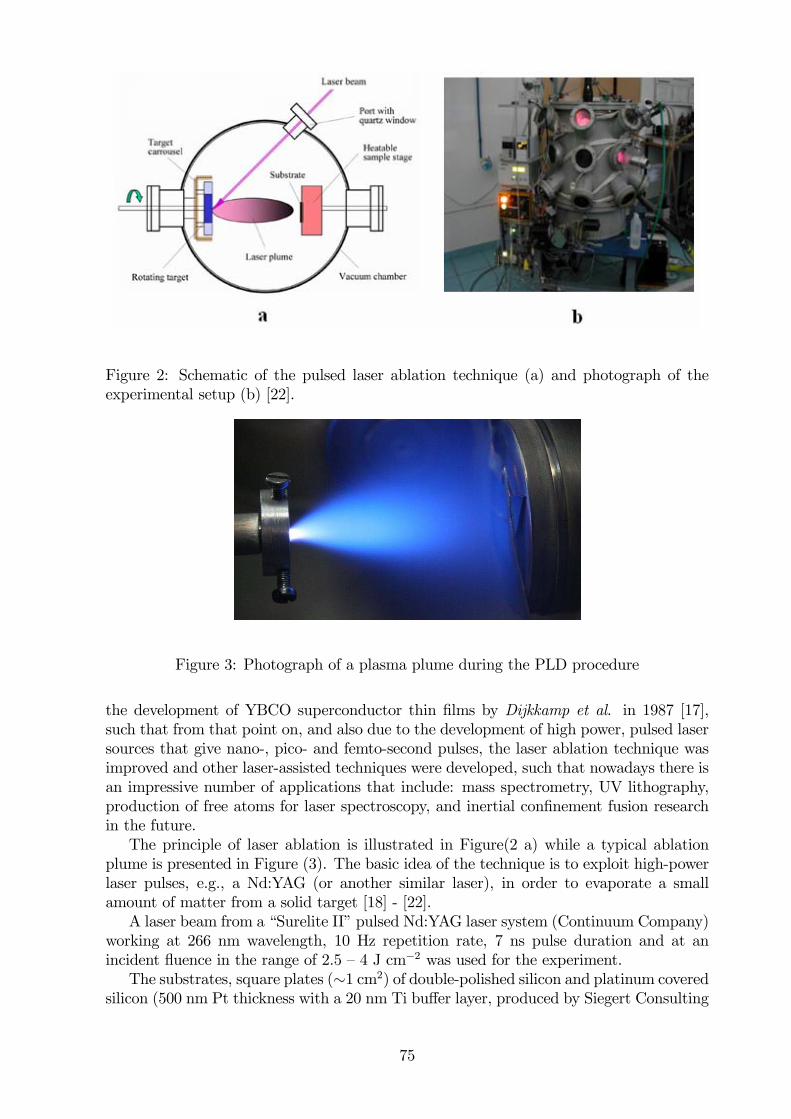
Figure 2: Schematic of the pulsed laser ablation technique (a) and photograph of theexperimental setup (b) [22].
Figure 3: Photograph of a plasma plume during the PLD procedure
the development of YBCO superconductor thin films by Dijkkamp et al. in 1987 [17],such that from that point on, and also due to the development of high power, pulsed lasersources that give nano-, pico- and femto-second pulses, the laser ablation technique wasimproved and other laser-assisted techniques were developed, such that nowadays there isan impressive number of applications that include: mass spectrometry, UV lithography,production of free atoms for laser spectroscopy, and inertial confinement fusion researchin the future.The principle of laser ablation is illustrated in Figure(2 a) while a typical ablation
plume is presented in Figure (3). The basic idea of the technique is to exploit high-powerlaser pulses, e.g., a Nd:YAG (or another similar laser), in order to evaporate a smallamount of matter from a solid target [18] - [22].A laser beam from a “Surelite II” pulsed Nd:YAG laser system (Continuum Company)
working at 266 nm wavelength, 10 Hz repetition rate, 7 ns pulse duration and at anincident fluence in the range of 2.5 — 4 J cm−2 was used for the experiment.The substrates, square plates (∼1 cm2) of double-polished silicon and platinum covered
silicon (500 nm Pt thickness with a 20 nm Ti buffer layer, produced by Siegert Consulting
75
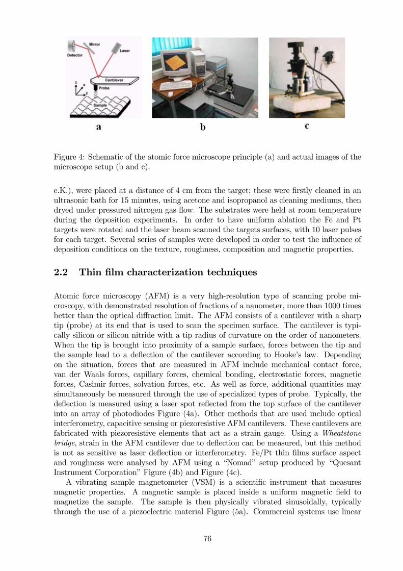
Figure 4: Schematic of the atomic force microscope principle (a) and actual images of themicroscope setup (b and c).
e.K.), were placed at a distance of 4 cm from the target; these were firstly cleaned in anultrasonic bath for 15 minutes, using acetone and isopropanol as cleaning mediums, thendryed under pressured nitrogen gas flow. The substrates were held at room temperatureduring the deposition experiments. In order to have uniform ablation the Fe and Pttargets were rotated and the laser beam scanned the targets surfaces, with 10 laser pulsesfor each target. Several series of samples were developed in order to test the influence ofdeposition conditions on the texture, roughness, composition and magnetic properties.
2.2 Thin film characterization techniques
Atomic force microscopy (AFM) is a very high-resolution type of scanning probe mi-croscopy, with demonstrated resolution of fractions of a nanometer, more than 1000 timesbetter than the optical diffraction limit. The AFM consists of a cantilever with a sharptip (probe) at its end that is used to scan the specimen surface. The cantilever is typi-cally silicon or silicon nitride with a tip radius of curvature on the order of nanometers.When the tip is brought into proximity of a sample surface, forces between the tip andthe sample lead to a deflection of the cantilever according to Hooke’s law. Dependingon the situation, forces that are measured in AFM include mechanical contact force,van der Waals forces, capillary forces, chemical bonding, electrostatic forces, magneticforces, Casimir forces, solvation forces, etc. As well as force, additional quantities maysimultaneously be measured through the use of specialized types of probe. Typically, thedeflection is measured using a laser spot reflected from the top surface of the cantileverinto an array of photodiodes Figure (4a). Other methods that are used include opticalinterferometry, capacitive sensing or piezoresistive AFM cantilevers. These cantilevers arefabricated with piezoresistive elements that act as a strain gauge. Using a Wheatstonebridge, strain in the AFM cantilever due to deflection can be measured, but this methodis not as sensitive as laser deflection or interferometry. Fe/Pt thin films surface aspectand roughness were analysed by AFM using a “Nomad” setup produced by “QuesantInstrument Corporation” Figure (4b) and Figure (4c).A vibrating sample magnetometer (VSM) is a scientific instrument that measures
magnetic properties. A magnetic sample is placed inside a uniform magnetic field tomagnetize the sample. The sample is then physically vibrated sinusoidally, typicallythrough the use of a piezoelectric material Figure (5a). Commercial systems use linear
76

Figure 5: Schematic of the VSM principle (a) and actual image of the LakeShore setup(b).
Figure 6: Schematic of the XRD principle (a) and actual image of the DRON DART UM2setup (b).
77

attenutators of some form and historically the development of these systems was doneusing modified audio speakers, though this approach was dropped due to the interferencethrough the in-phase magnetic noise produced, as the magnetic flux through a nearbypickup coil varies sinusoidally. The induced voltage in the pickup coil is proportionalto the sample’s magnetic moment, but does not depend on the strength of the appliedmagnetic field. In a typical setup, the induced voltage is measured through the use of alock-in amplifier using the piezoelectric signal as its reference signal. By measuring in thefield of an external electromagnet, it is possible to obtain the hysteresis curve of a material.Vibrating sample magnetometry was performed for specific magnetic characterization ona LakeShore setup Figure (5b).X-ray crystallography is an important method of determining the arrangement of
atoms within a crystal in which a beam of X-rays strikes a crystal and diffracts into manyspecific directions. If X-rays of known wavelength strike a crystal whose lattice planes areseparated by a distance d, the radiation will be strongly reflected at angles which satisfyBragg’s Law:
λ = 2d sin θWhen the values of θ and 2θ are known, the corresponding values of d can be cal-
culated. Using the calculated values of d it is possible to extrapolate a great deal ofinformation about the sample: from the angles and intensities of these diffracted beams,a crystallographer can produce a three-dimensional picture of the density of electronswithin the crystal. From this electron density, the mean positions of the atoms in thecrystal can be determined, as well as their chemical bonds, their disorder and variousother information (qualitative and quantitative mineral content, crystallographic struc-ture determination, identification of unknown substances). Figure (6a) shows a commonconfiguration for an XRD unit. Full featured units are upgradeable with additional hard-ware to optimize the instrument for single thin film measurements, crystal analysis, highspeed diffraction scanning, high resolution diffraction, bath ratio and many other specialapplications. Bench-top models are available, however, their functionality is severely lim-ited making them extremely inflexible and narrow in their area of application. For thisexperiment a DRON DART UM2 diffraction setup was used, presented in Figure (6b).
3 Results and discussion
3.1 The AFM technique
The AFM images of the Fe/Pt samples are presented in Figure (7). The surface of thesamples appear to be uniformly covered and relatively smooth Figure (7a), with onlysmall droplets present on the surface Figure (7b) and Figure (7c); the root mean squaredeviation (RMS deviation) is 8.025 nm. As an extrinsic property the coercivity of a thinfilm strongly depends on the internal and, more impotant, the surface microstructurebut this aspect is to be detailed when the magnetic properties of the Fe/Pt samples arediscussed.
3.2 The XRD technique
In Figure (8) it is shown the XRD pattern of as-deposited Fe/Pt thin films. The thinfilms exhibit peaks of disordered face-centered cubic (fcc), but also ordered face-centeredtetragonal (fct) planes (001) at about 210 and (111) at about 380; the dominant phase isthe fct Fe/Pt phase. The intensities of the Fe/Pt (001) peak increases as Fe/Pt thickness
78

Figure 7: AFM images of the thin film surface (RMS deviation: 8.025 nm): 2μm23Dshape lines (a) and surface characteristics (b); 10μm2 2D image of a thin film (c).
79

Inte
nsita
te (u
.a)
0
200
400
600
800
1000
2 θ
10 20 30 40 50
--- FePt - tetragonal
Figure 8: XRD spectrum of the Fe/Pt as-deposited thin films.
Figure 9: Schematic illustration of the unit cell of (A) chemically disordered fcc and (B)chemically ordered fct Fe/Pt (b) (source of the images: Brown University).
increased to at least 10 nm. The origin of fct Fe/Pt (001) texture evolution in the filmswas due to the occurrence of anisotropic strain during ordering transformation [2], [7], [8],[23], [24]; a schematic is presented in Figure (9). Thus, the Fe/Pt (001) texture could beobtained by PLD of atomic-scale layer of Fe and Pt deposition.
3.3 The VSM technique
Perpendicular magnetic anisotropy (PMA) was observed in the films after at least 15repetitions (N = 15) of Fe/Pt deposition [24] - [27]. A steady increase in the coercivefield (HC) was found with an increase in the number of bilayers from 5 to 16 but thenHC levels off for N > 16. The latter can be attributed to an increase in the number ofstructural defects with increasing bilayer number affecting the interface quality and thuseventually resulting in an overall reduction of the magnetic anisotropy [25]. The dropletsobserved by AFM may be a source of magnetic pinning in domain magnetization reversal,which can lead to a (small) increase in thin film coercitivity, but the actual origin of this
80

Figure 10: Hysterezis loops measured in the out-of-plane geometry for the FePt thin filmsdeposited at room temperature [10].
enhancement of the coercive field is not yet completly clear.Several hysterezis loops of the Fe/Pt samples are presented in Figure (10). Such a
perpendicular magnetic anisotropy could improve the writability and signal-to-noise ratioin magnetic recording media.
4 Conclusions
Pulsed laser-assisted deposition techniques are clean, simple yet versatile methods thatallow good control in thin films and/or multilayer-structured samples. We have preparedand investigated the magnetic properties and microstructures of nanometer-size Fe/Ptfilms on silicon and platinum covered silicon substrates, at room temperature. The surfacemorphology of the films reveal a relatively smooth surface with only few small (under 50nm) droplets. The XRD patterns reveal the crystalline structure of the films, while theVSM measurements show that perpendicular anysotropy is present.
References
[1] N. Honda, S. Takahashi, K. Ouchi, J. Magn. Magn. Mater. 320 (2008) 2195.
[2] Y.S. Yu, Hai-Bo Li, W.L. Li, Mei Liu, Yu-Mei Zhang, W.D. Fei, D.J. Sellmyer, ThinSolid Films 518 (2010) 2171.
[3] S. Sun, C.B. Murray, D.Weller, I. Folks, A. Moser, Science 287 (2000) 1989.
[4] L.C. Varanda, M. Jafelicci Jr., M. Imaizum, J. Appl. Phys. 101 (2007) 123918.
[5] S. Fujji, S. Ishida, S. Asano, J. Phys. Soc. Jpn. 59 (1989) 3657.
[6] M. Imaizumi, C.A. Soufen, C.A.F. Pintão, L.C. Varanda, M. Jafelicci Jr., Mat. Sci.Eng. A 521—522 (2009) 167.
81

[7] G.P. Lin, P.C. Kuo, K.T. Huang, C.L. Shen, T.L. Tsai, Y.H. Lin, M.S. Wu, ThinSolid Films 518 (2010) 2167.
[8] P. Schaaf , K. Zhang, C. Lange, A. Holz, M. Weisheit, S. Fahler, Appl. Surf. Sci. 253(2007) 8107.
[9] L.J. Qiu, J. Ding,A.O. Adeyeye, J.H. Yin, J.S. Chen, S. Goolaup, N. Singh, IEEETrans. Magn. 43 (2007) 2157.
[10] A. Perumal, Y. K. Takahashi, K. Hono, J. Appl. Phys. 105 (2009) 07B732.
[11] Z.H. Lu, M.J. Walock, P. LeClair, W.H. Butler, G.J. Mankey, J. Vacuum Sci. Tech.A 27 (2009) 1067.
[12] L.Y. Han, U. Wiedwald, B. Kuerbanjiang, P. Ziemann, Nanotechnology 20 (2009)285706.
[13] S.W. Wang, A.C. Sun, F.T. Yuan, J.H. Hsu, P.C. Kuo, IEEE Trans. Magn. 45 (2009)3580.
[14] M. Koz1owski, R. Kozubski, Ch. Goyhenex, V. Pierron-Bohnes, M. Rennhofer, S.Malinov, Intermetallics 17 (2009) 907.
[15] T. H. Maiman, Phys. Rev. Lett. 4 (1960) 564.
[16] H. M. Smith, A. F. Turner, Appl. Opt. 4 (1965) 147.
[17] D. Dijkkamp, T. Venkatesan, X. D. Wu, S. A. Shaheen, N. Jisrawi, Y. H. Min-Lee,W. L. McLean, M. Croft, Appl. Phys. Lett. 51 (1987) 619.
[18] J. C. Miller (editor), “Laser Ablation - Principles and Applications”, Springer-Verlag,Berlin, 1994.
[19] D. B. Chrisey, G. K. Hubler (editors), “Pulsed Laser Deposition of Thin Films”, JohnWiley & Sons Inc., New York, 1994.
[20] D. B. Chrisey, R.W. Eason (editors), “Pulsed Laser Deposition of Thin Films: Ap-plications in Electronics, Sensors, and Biomaterials”, John Wiley & Sons Inc., NewYork, 2007.
[21] M. von Allmen, A. Blatter (editors), Laser-Beam Interactions with Materials,Springer-Verlag, Berlin, 1995.
[22] www.physandtech.net
[23] Z.Y. Pan, R.S. Rawat, J.J. Lin, T. Zhang, P. Lee, T.L. Tan, S.V. Springham, Appl.Phys. A 96 (2009) 1027.
[24] S. Sun, Advanced Materials 18 (2006) 393.
[25] D. Makarov, J. Lee, C. Brombacher, C. Schubert, M. Fuger, D. Suess, J. Fidler, M.Albrecht, Appl. Phys. Lett. 96 (2010) 062501
[26] J.Y. Ahn, N.J. Lee, T.H. Kim, J. Magn 14 (2009) 144.
[27] J.L. Tsai, H.T. Tzeng, G.B. Lin, Appl. Phys. Lett. 96 (2010) 032505.
82


![Materials Chemistry and Physics - University of Malaya · PDF fileto develop thin films of nanometer thickness, nano sized particles, nanorodsandsheets[5,6].Itisaknownquantummechanicaleffect](https://static.fdocuments.us/doc/165x107/5a9fc4597f8b9a62178d268e/materials-chemistry-and-physics-university-of-malaya-develop-thin-lms-of-nanometer.jpg)