Nano-scale Science and Technology: An Overview · PDF fileNano-scale Science and Technology:...
42
1 1 Nano-scale Science and Technology: An Overview Om Prakash Khatri Nanoscopic Surface Architecture Laboratory Department of Materials Science and Engineering Kyoto University, Kyoto 14 th June 2007
-
Upload
trinhkhuong -
Category
Documents
-
view
221 -
download
4
Transcript of Nano-scale Science and Technology: An Overview · PDF fileNano-scale Science and Technology:...

11
Nano-scale Science and Technology: An Overview
Om Prakash Khatri
Nanoscopic Surface Architecture LaboratoryDepartment of Materials Science and Engineering
Kyoto University, Kyoto
14th June 2007

22
Nano-scale Science and Technology
“Study of objects, phenomena and/or manipulation of physical system over 1-100 nanometer scale”
1 nm = 10-9 m = One billionth of meter
× 101 nm
Hydrogen AtomDiameter = 0.1 nm

33
Comparison Between Human Size and Nano
44
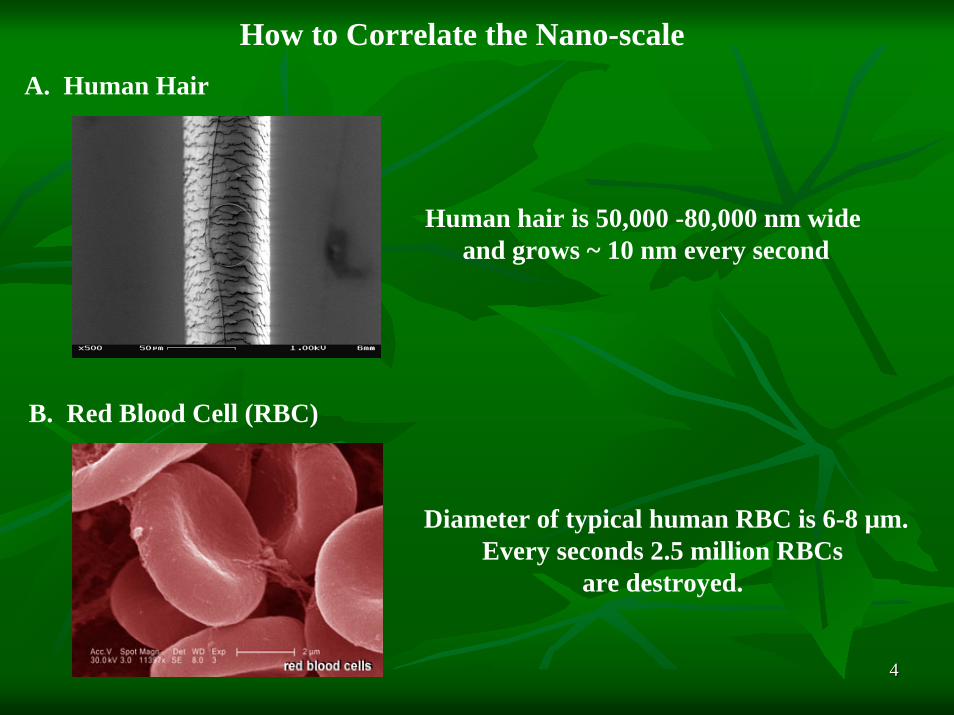
How to Correlate the Nano-scaleA. Human Hair
Human hair is 50,000 -80,000 nm wide and grows ~ 10 nm every second
B. Red Blood Cell (RBC)
Diameter of typical human RBC is 6-8 µm.Every seconds 2.5 million RBCs
are destroyed.

55
C. Human Immunodeficiency Virus (HIV)
Diameter of HIV virus is 120 nm, which causes AIDS disease
D. DNA structure
DNA is 2.2 to 2.4 nm wide and made from repeating units of Nucleotides

66
How Nano is Big: Everything is Changing
77
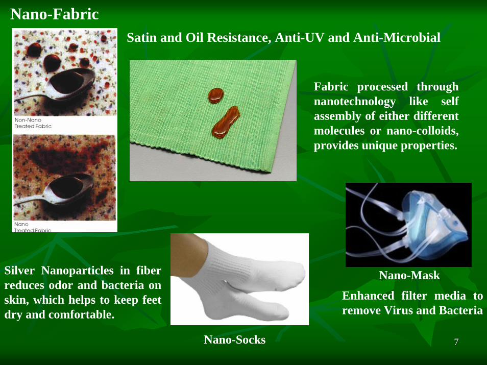
Nano-FabricSatin and Oil Resistance, Anti-UV and Anti-Microbial
Fabric processed through nanotechnology like self assembly of either different molecules or nano-colloids, provides unique properties.
Nano-MaskSilver Nanoparticles in fiber reduces odor and bacteria on skin, which helps to keep feet dry and comfortable.
Enhanced filter media to remove Virus and Bacteria
Nano-Socks

88
Nano-Cosmetics
Zinc oxide particles: Sun CreamSuperfine Silica Particles: Skin CreamBuckyballs: Prevents premature aging of the skin by acting as antioxidant
Buckyballs
Nano-Sports
Golf: Nano-composite makes the top part of driver more lighter, which helps the golfer to hit with more power and accuracy.
Tennis: Nano-tube makes more stronger and light racket
Bowling: Fullerenes uses as a super-hard coating on bowling balls.
99
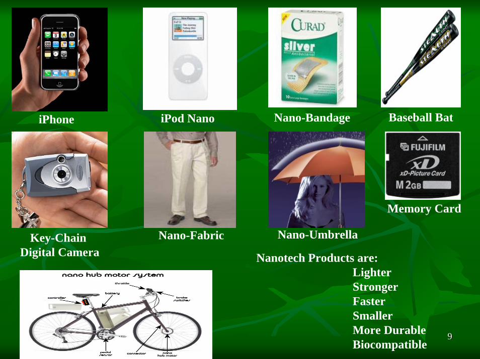
Baseball BatNano-BandageiPod NanoiPhone
Memory Card
Nano-UmbrellaNano-FabricKey-Chain Digital Camera Nanotech Products are:
LighterStrongerFasterSmallerMore DurableBiocompatible

1010
How do we build so small: Nanofabrication
Top-down Approach
Construct the nanostructure, starting with a larger component by remove or alter the material
1. Photo Lithography2. Soft Lithography (Micro Contact Printing)3. Scanning Probe based Lithography etc.
Bottom-up Approach
Formation of small devices or nanostructures from molecules or atoms
1. Self assembly process (molecules, colloidal particles etc)2. Carbon Nanotubes etc

1111
Photolithography
Photolithography is a process, which remove parts of a thin film (or the bulk of a substrate), by light exposure through Photo-mask
1. Light Source: Deep Ultraviolet (DUV) light below 300 nm wavelengths
2. Minimum Pattern Size: 100 nm
3. Mass Production
Gold Nanoparticles arrays

1212
How we makes Photo-pattern1. Clean the substrate
Silicon
Silicon oxide
4. Unexposed molecular Film
Silicon2. Formation of molecular Film
5. Oxide film etched away from Hydrofluoric acidSilicon
Silicon
3. Silicon is exposed to UV light through Photo-mask
UV Radiation
Photo-mask
Silicon
1313
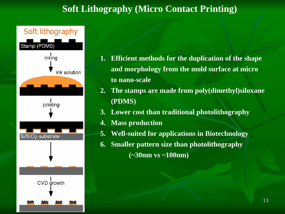
Soft Lithography (Micro Contact Printing)
1. Efficient methods for the duplication of the shape and morphology from the mold surface at micro to nano-scale
2. The stamps are made from poly(dimethyl)siloxane(PDMS)
3. Lower cost than traditional photolithography 4. Mass production 5. Well-suited for applications in Biotechnology6. Smaller pattern size than photolithography
(~30nm vs ~100nm)

1414
Soft Lithography
Fluorescence microscopy images of arrays of (A) 10 um, (B) 5 um spots of Texas-Red labelled Streptavidin/Biotin complex by micro-contact printed on poly(methyl methacrylate)
Micro-contact printing, in which a weakly bound film is displaced by contact stamping with molecules
that bind more strongly to the substrate

1515
Dip Pen Lithography
AFM tip is used to deliver molecules to a surface via a solvent meniscus. This direct-write technique offers high-resolution patterning capabilities for a number of molecular and bio-molecular or colloidal ink and they forms a self assembled monolayer. Sub-100nm length scale features are fabricated by this method.
Courtesy: Prof. C. Mirkin Group

1616
Self Assembled Monolayer
“A two-dimensional film, one molecule thick, covalently organized or assembled at an interface”

1717
Why self assembly system is important
1. Reduces the Friction and Adhesion: Lubrication engineering
2. Chemical Biological Sensors

1818
3. Patterning
A patterned SAM with alternating COOH-terminated and CH3 stripes
4. Wettability
Hydrophobic
Hydrophilic
1919
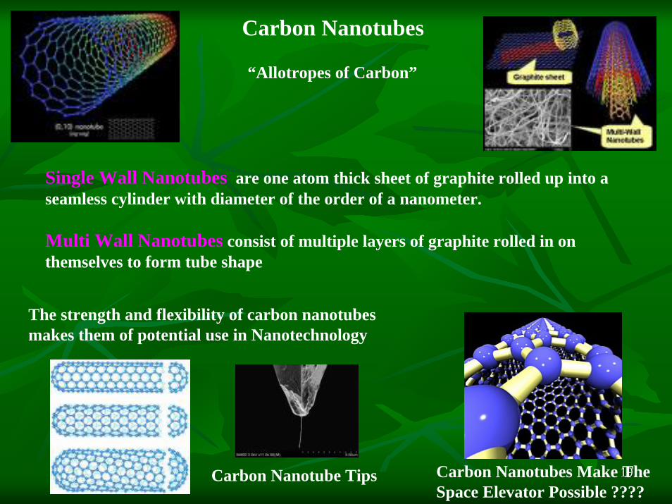
Carbon Nanotubes
“Allotropes of Carbon”
Single Wall Nanotubes are one atom thick sheet of graphite rolled up into a seamless cylinder with diameter of the order of a nanometer.
Multi Wall Nanotubes consist of multiple layers of graphite rolled in on themselves to form tube shape
The strength and flexibility of carbon nanotubes makes them of potential use in Nanotechnology
Carbon Nanotubes Make The Space Elevator Possible ????
Carbon Nanotube Tips

2020
Nanoparticles
The chemical properties (reactivity, flammability, etc.) and the physical properties (melting point, conductivity, optical property etc.) all changes at the nano-scale. Size-dependent properties are the major reason, that nano-scale objects have such amazing potential.
m.p. bulk
1000
Tm
eltin
g(°
C)
500
00 5 10 15 20
Gold Nanoparticles Particle Diameter (nm)
Melting point of gold as a function of gold particle diameter
2121
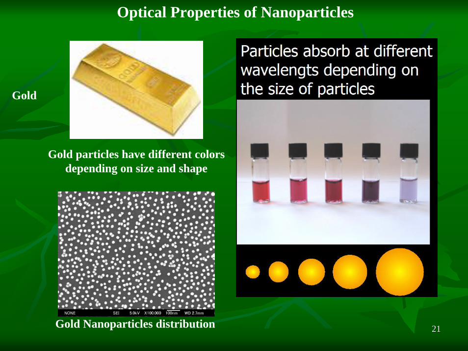
Optical Properties of Nanoparticles
Gold particles have different colors depending on size and shape
Gold Nanoparticles distribution
Gold

2222
Scanning Probe Microscope“Image of the surfaces using a physical probe that scans the specimen”
1. Atomic Force Microscopy
“Measure the surface features due to atomic force interaction between tip & sample”A. Contact AFM,B. Non-contact AFM and C. Dynamic contact AFM
2. Scanning Tunneling Microscopy
“Detect a weak electric current flowing between tip and the surface”
3. Magnetic Force Microscopy
“Magnetic interaction between tip and samples”
4. Kelvin Force Microscopy
“Work function or chemical contrast of surfaces can be observed at nano-scales”

2323
How AFM Works

2424
What information, we gets from SPM
Surface Roughness at Atomic level (Topography)
AFM friction: NaCl (100)

2525
3. Biological Features
Butterfly wing
4. STM atomic resolution on HOPG (Highly Oriented graphite with atomic resolution)

2626
Nanoflower grown by deposition of antimony on a smooth carbon surface
Atomic Resolution on Si (111); 5.4nm x 5.4nm
Enzyme-substrate Interactions

2727
To Measure Adhesive Force for Biological Systems
By pulling on fimbriae with the tip of an AFM, provides mechanical properties that helped to elucidate their function.

2828
Nanotechnology in Biological Systems
1. Hip Implant Materials
Nano-scale modification of implant surfaces would improve implant durability and biocompatibility
2. Nano-Robots
The nano-robot is using rotary blades to break up the blockage and sucking the fragments into nozzles
Nano-Robot swimming through human vein
2929
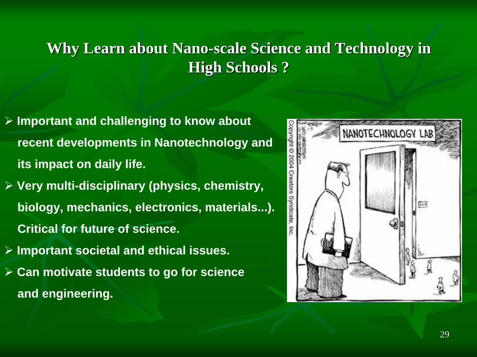
Why Learn about NanoWhy Learn about Nano--scale Science and Technology in scale Science and Technology in High Schools ?High Schools ?
Important and challenging to know about
recent developments in Nanotechnology and
its impact on daily life.
Very multi-disciplinary (physics, chemistry,
biology, mechanics, electronics, materials...).
Critical for future of science.
Important societal and ethical issues.
Can motivate students to go for science
and engineering.
3030
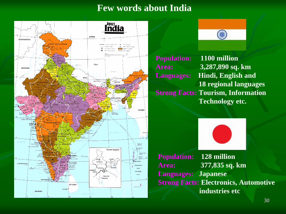
Few words about India
Population: 1100 millionArea: 3,287,890 sq. kmLanguages: Hindi, English and
18 regional languagesStrong Facts: Tourism, Information
Technology etc.
Population: 128 millionArea: 377,835 sq. kmLanguages: JapaneseStrong Facts: Electronics, Automotive
industries etc

3131
India
The Indus Valley civilization, one of the oldest in the world
28 States and 7 Union Territories
National Capital: Delhi
Literacy: 61%
Government: Federal Republic
Religions
1.9%1.9%2.3%
13.4%
OthersSikh
Christian
MuslimHindu
National Costume: Sari (Women)National Bird: PeacockNational Fruit: Mango

3232
India: Tourism Facts
Tajmahal, Agra“One of the Beautiful Wonder of the world”
Rishikesh, Holy city for Hindus located in the foothills of the Himalaya
Lake Palace, UdaipurWonderful beaches: Lakshadeep
3333
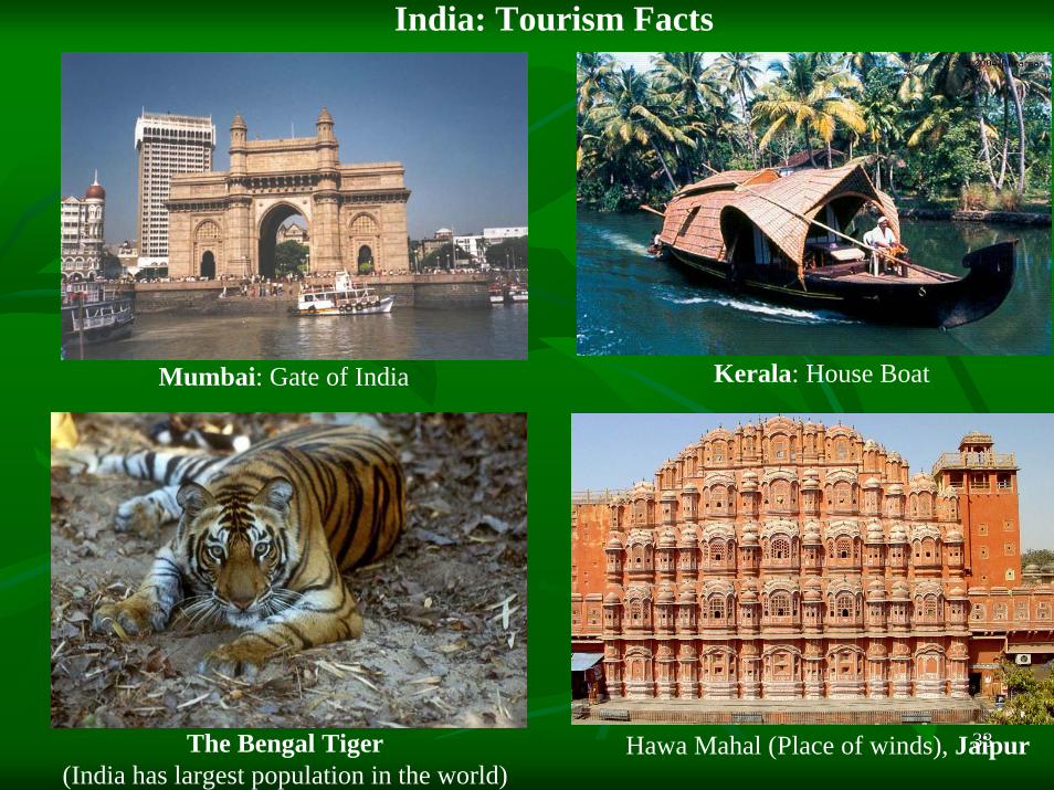
India: Tourism Facts
Mumbai: Gate of India Kerala: House Boat
The Bengal Tiger(India has largest population in the world)
Hawa Mahal (Place of winds), Jaipur

3434
India: Cultural FactsIndian Dances
Indian Women
KashmirRajasthan Punjab

3535
Indian Education System

3636
LKG, UKG(Age: 3-5)
Class 1-5(Age: 6-11)
Class 6-10(Age: 11-16)
Class 11-12(Age: 16-18)
Nursery Primary Secondary Higher Sec
Engineering: 4 Years
Medical: 5 Years
Science: 3 Years
Commerce: 3 Years
Arts: 3 Years
Master Degree(2-3 years) Research: Ph.D.Higher Secondary

3737
“ELEMENTARY EDUCATION IS FUNDAMENTAL RIGHT FOR EVERY CHILD IN INDIA”
Indian culture is in the core attributes of education beginning from GURUKUL type of education, where the disciples lived in the house of master who taught them.
IndianEducation
System
931500Schools45000
Colleges
300U
niversities

3838
Elementary Schooling
All children should complete eight years elementary schooling: Government of India
Modern Elementary Schools
School fee are very high compared to Government schools

3939
High School Education
High School Education is very important to decide Future Goals.Subjects Specialization starts from High Schools. Like Science, Arts, Commerce etc
College/University/InstituteEntrance Examination
And/orDirect Merit Basis
High Schools

4040
Higher EducationOver 300 UniversitiesCovers all disciplines like Science, Engineering, Medical, Pharmaceuticals, Agriculture, Managements, Humanities, Commerce, Dairy & Fisheries and Fashion designing etc Tough competition to get admission in Good University/InstitutesMost of Universities or Institutes are Funded by Government. Pune University
Indian Institute of Technology, Roorkee
Indian Institute of Science, Bangalore
4141
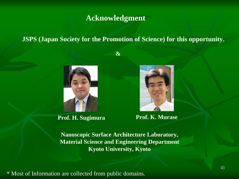
Acknowledgment
JSPS (Japan Society for the Promotion of Science) for this opportunity.
&
Prof. K. MuraseProf. H. Sugimura
Nanoscopic Surface Architecture Laboratory,Material Science and Engineering Department
Kyoto University, Kyoto
* Most of Information are collected from public domains.