Multiscale Dynamic Materials Modeling Dept. 1435
55
HΨ = E Ψ From density functional theory to defect levels in silicon: Does the “band gap problem” matter? Sandia is a multiprogram laboratory operated by Sandia Corporation, a Lockheed Martin Company, for the United States Department of Energy’s National Nuclear Security Administration under contract DE-AC04-94AL85000. Peter A. Schultz Multiscale Dynamic Materials Modeling Dept. 1435 Sandia National Laboratories, Albuquerque, NM 87185 Purdue University, Thursday, August 21, 2008 It is the mark of an educated mind to rest satisfied with the degree of precision which the nature of the subject admits and not to seek exactness where only an approximation is possible. - Aristotle SAND2008-5669P
Transcript of Multiscale Dynamic Materials Modeling Dept. 1435

HΨ = E Ψ
From density functional theory todefect levels in silicon:
Does the “band gap problem” matter?
Sandia is a multiprogram laboratory operated by Sandia Corporation, a Lockheed Martin Company,for the United States Department of Energy’s National Nuclear Security Administration
under contract DE-AC04-94AL85000.
Peter A. SchultzMultiscale Dynamic Materials Modeling Dept. 1435
Sandia National Laboratories, Albuquerque, NM 87185
Purdue University, Thursday, August 21, 2008
It is the mark of an educated mind to rest satisfied with the degreeof precision which the nature of the subject admits and not to seekexactness where only an approximation is possible.
- Aristotle
SAND2008-5669P

2 Purdue - Aug. 21, 2008
Pete
r A
. Sch
ultz
Motivation:Electrical effects of radiation damage
Systems responseRadiation testingn,e,γ,ions
Issue: radiation effects (n,e,γ,ions) on electronics- satellites- weapon electronics
Historical approach: radiation testing
Renewed interest: - long-term aging: enhanced low dose rate sensitivities
long-term (decades) radiation damage is different- fast transients: SPR facility decommission
fast burst neutron test facility going away

3 Purdue - Aug. 21, 2008
Pete
r A
. Sch
ultz
Radiation damage: from atoms to devices
Initial defect distribution
Defect evolution
Radiation creates displacement damage:R → V + I
and charge carriers (electrons and holes)R → n + p
Defects react with each other, andwith other dopants and impurities:
V + I → SiSi
Defects recombine electrons andholes, modifying currents:
T0 + n → T-
T- + p → T+
Radiation damage creates an evolving chemistry of defects.Those defects modify the performance of electronic devices.

4 Purdue - Aug. 21, 2008
Pete
r A
. Sch
ultz
Multiscale ladder for radiation damage
Electrical system responseTe
stin
g
DFT /ATOMISTIC
DEVICE models
CIRCUIT modelsEXPT
EXPT
EXPT
Radiation damage

5 Purdue - Aug. 21, 2008
Pete
r A
. Sch
ultz
The radiation defect universe
Si interstitial (i)i(+2,+1,0,–1,–2)
Vacancy (v)v(+2,+1,0,–1,–2)
Bi (+,0,–)
Primary defects … secondary defects … and more
Ci (+,0, –)
vO (0,–)
vP (0,–)
vB (+,0)
vv(+1,0,-1,-2)
BiB (0,–)
BiO (+,0)
BiC (?)
Annihilation+ what we don’tknow we don’tknow (discovery)
Dopants:BSi, PSi , AsSi
Impurities:CSi, Oi
Need DFT - density functional theory - to fill gaps in defectphysics: defect band gap energy levels, diffusion activation

6 Purdue - Aug. 21, 2008
Pete
r A
. Sch
ultz
What do we know, what do we need?
•Experimental record incomplete and messy- defect level measurements typical Uncertainty(U): ≥ kT ~ 0.03 eV
e.g.: S(2+/+): optical CB -0.61, thermal: -0.55:-0.59vv(0/+): VB+0.20:+0.26, vv(-/0): CB-0.39:-0.44
- often larger: Bi(-/0): U=0.08, Ns(0/+): U=0.12, Bv: a mess (U~0.10)- U(expt) = 0.03 eV (best), ~0.1 eV (otherwise)- incomplete knowledge (Bv, Pv, BiX, …) … U=∞
•Density functional theory: unproven for levels- DFT structural energetics accurate to no better than ~0.1-0.2 eV- best accuracy to hope for with DFT: ~0.1-0.2 eV
•Accuracy requirement: kT=0.03 eV?, 0.1-0.2 eV?- if 0.03 eV, then even experiment is not good enough - we’re doomed- current device (CHARON, REOS, 1D) simulations using 0.1 eV data- apparent target requirement: 0.1 eV (device sims, and expt. record)

7 Purdue - Aug. 21, 2008
Pete
r A
. Sch
ultz
Radiation damage and defects
CB
VB
produces defects … and introduces electronic transitions
… and we would like to quantify these transitions
Radiation damage …

8 Purdue - Aug. 21, 2008
Pete
r A
. Sch
ultz
The DFT band gap problem
Conduction Band
Valence Band
Band gap
Experiment Kohn-Sham DFT eigenvalue spectrum
DFT gap. i.e., in KS eigenvalues, significantly underestimates experiment[L.J. Sham and M. Schlüter, PRL 51, 1888 (1983); PRB 32, 3883 (1985)]Si: expt: 1.2 eV, DFT/LDA: 0.5 eVGaAs: expt. 1.5 eV, DFT/LDA: 0.5 eV
The band gap defines the energy scale for defect levels
Fundamental impediment to quantitative predictions?
9 Purdue - Aug. 21, 2008
Pete
r A
. Sch
ultz
The Supercell Approximation
Finite defect
Fast Fourier Transforms are convenient means to solve 3D Poisson Equation.
DFT codes typically assume periodic boundary conditions.
However, our finite defect is not periodic …

10 Purdue - Aug. 21, 2008
Pete
r A
. Sch
ultz
The Supercell Approximation
Finite defect Periodic (interacting?) defects
Fast Fourier Transforms are convenient means to solve 3D Poisson Equation.
DFT codes typically assume periodic boundary conditions.
However, our finite defect is not periodic …
supercellapproximation
The supercell Idea:Surround perturbed defect region with enough material to buffer defects.In the limit of large enough supercells, approach an isolated defect.

11 Purdue - Aug. 21, 2008
Pete
r A
. Sch
ultz
The Supercell Approximation
Finite defect with dipole Periodic (interacting) defects
DFT expense limits size of supercell - defects interact
the catch …

12 Purdue - Aug. 21, 2008
Pete
r A
. Sch
ultz
The Supercell Approximation
Finite defect with dipole Periodic (interacting) defects
Finite charged defect Ill-defined (Coulomb divergence)
Interactions and divergence are key issues
the catch …
even worse …

13 Purdue - Aug. 21, 2008
Pete
r A
. Sch
ultz
Supercell issues
And if you get this all right … is DFT good enough?- e.g., is the band gap problem fatal?
• Boundary conditions - how to handle net charge- need to eliminate divergence- need to install correct long range q/r -> 0 behavior of defect charge
• Chemical potential for electrons- want transition energies, (0/-), (0/+), need to fix an electron reservoir
• Finite size effects - Bulk polarization to local charge- supercell has small finite volume, missing bulk dielectric response
• Finite size effects - Defect level dispersion- defects interact, discrete defect states become bands, overlap CB/VB

14 Purdue - Aug. 21, 2008
Pete
r A
. Sch
ultz
Jellium to eliminate divergence?
Apply supercell …
Isolated defect …
Neutralize with flat background charge:“jellium”
15 Purdue - Aug. 21, 2008
Pete
r A
. Sch
ultz
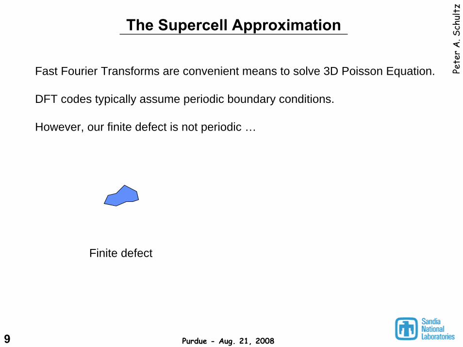
Whence the divergence?
supercell
q/r q/r

16 Purdue - Aug. 21, 2008
Pete
r A
. Sch
ultz
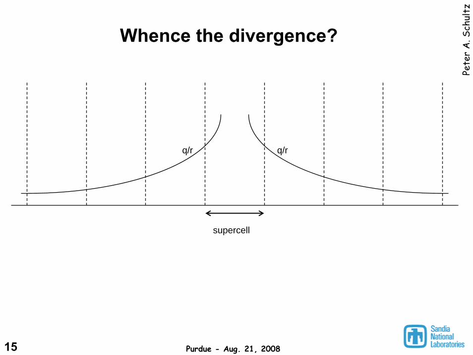
Whence the divergence?
supercell
q/r q/rq/rq/r
17 Purdue - Aug. 21, 2008
Pete
r A
. Sch
ultz
Whence the divergence?
supercell
q/r q/rq/r q/rq/r q/r

18 Purdue - Aug. 21, 2008
Pete
r A
. Sch
ultz
Whence the divergence?
supercell
q/r q/rq/r q/r q/rq/r q/r q/r

19 Purdue - Aug. 21, 2008
Pete
r A
. Sch
ultz
Whence the divergence?
supercell
∞
q/r q/rq/r q/r q/r q/rq/r q/r q/r q/r
Divergence arises from infinite-ranged q/r potentials from periodic images
Divergence is not flat
20 Purdue - Aug. 21, 2008
Pete
r A
. Sch
ultz
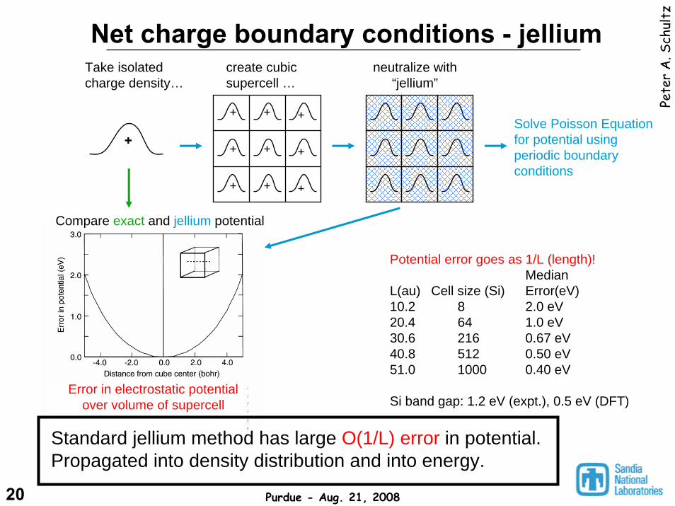
Net charge boundary conditions - jelliumTake isolatedcharge density…
Error in electrostatic potentialover volume of supercell
Potential error goes as 1/L (length)!Median
L(au) Cell size (Si) Error(eV)10.2 8 2.0 eV20.4 64 1.0 eV30.6 216 0.67 eV40.8 512 0.50 eV51.0 1000 0.40 eV
Si band gap: 1.2 eV (expt.), 0.5 eV (DFT)
+
create cubicsupercell …
neutralize with“jellium”
Solve Poisson Equationfor potential usingperiodic boundaryconditions
Standard jellium method has large O(1/L) error in potential.Propagated into density distribution and into energy.
Compare exact and jellium potential

21 Purdue - Aug. 21, 2008
Pete
r A
. Sch
ultz
Local Moment CounterCharge (LMCC)[ P.A. Schultz, PRB 60, 1551 (1999); PRL 84, 1942 (2000) ]
• Solution of Poisson Equation is linear in the density• LMCC: split total density ρ( r ) into two pieces …
(1) model local density ηLM( r ) matching multipole (charge) of ρ( r )(2) remainder (momentless) density ρ’( r ) = ρ( r ) - ηLM( r )
= +ρ( r ) ηLM( r ) ρ’def( r )
φ( r ) φLM( r ) φ’def( r )
= +
PBC (e.g. fft)LBC ( q/r -> 0 )
Gives proper r→∞ asymptotic boundary conditionAvoids (not ignores!) Coulomb divergence

22 Purdue - Aug. 21, 2008
Pete
r A
. Sch
ultz
A practical method for LMCC
= +ρ( r ) ηLM( r ) ρ’def( r )
Requirements:(a) ηLM( r ) contains the local moments(charge) to be solved(b) ηLM( r ) is spatially slowly varying — fft-able(c) ηLM( r ) is entirely localized within cell — define vacuum(d) potential φ( r ) associated with ηLM( r ) is easily evaluated
Usual suspects:- point charges violate (b)- Jellium (flat background) violates (a), (c), and (d)
One (not unique) solution: sum of Gaussians: ηg(r) = exp( - α r2 )ηLM( r ) = Σ cg ηg(r – Rg)
For charged system: one gaussianFor dipole: pair of gaussiansQuadrupoles and above neglected (good to O[L–5] )

23 Purdue - Aug. 21, 2008
Pete
r A
. Sch
ultz
Charged cell convergence - Jellium method
w/jellium self-energy corrections
w/o jellium self-energy
Figure 3
Variation in computed total energy due to incorrect charge potential
cell size (side length) cell size (side length)
Mg
atom
ioni
zatio
n po
tent
ial

24 Purdue - Aug. 21, 2008
Pete
r A
. Sch
ultz
Charged cell convergence - LMCC method
LCharged, no dipole: CH4 → CH4[+] … Ionization Potential
L = 18.0 - 30.0 bohr (9.5-15.9 Å) IP varies < 10–5 eV
Dipole, no charge: Na–Cl diatomic molecule … Total Energy
L = 16.8 - 30.0 bohr (8.9-15.9 Å) TE varies < 10–5 eV
Dipole, charge: OH → OH[-] … Electron Affinity
L = 18.0 - 30.0 bohr (9.5-15.9 Å) EA varies < 10–3 eV
CH HHH CH H
HH
Total energy, levels, i.e. full Hamiltonian are all immediately converged.-> electrostatic potential correctly represented by LMCC, not just energyP.A. Schultz, PRB 60, 1551 (1999)

25 Purdue - Aug. 21, 2008
Pete
r A
. Sch
ultz
LMCC potential in bulk systemsWhat is the problem?
← supercell repeat →
pote
ntia
l
Discontinuity in potential from LMCC at supercell boundary!
The solution: Wigner-Seitz cells around LMCC positions
With WS local volume, LMCC potential is continuous

26 Purdue - Aug. 21, 2008
Pete
r A
. Sch
ultz
LMCC: NaCl, Cl vacancy ionization1D
cha
in2D
she
et3D
bul
k
Supercell size dependence due to polarization.Larger supercell -> more polarizationApparent L–3 scaling = 1D classical dielectric screening
1D:
2D:
3D:
single-layer 2D square sheet (polar&non-polar)
Apparent L–2 scaling = 2D classical dielectric screening
Insensitive to cell type, polar vs. non-polar
bulk-layer 3D square sheet (fcc&sc cells)
Apparent L–1 scaling = 3D classical dielectric screeningStrictly screening due to large supercell volumeInsensitive to cell shape

27 Purdue - Aug. 21, 2008
Pete
r A
. Sch
ultz
How do you set an energy zero for charge?Kleinman [PRB 24, 7412 (1981)]: cannot do it in bulk!
Garcia, Northrup, Van de Walle, others: empirical band alignment- take band feature (e.g., VB, CB,) in defect calculationand “align” with similar feature in bulk calculation
CB
VB
CB
VB
(-)
defect bandstructure crystal band
structure
Problems with standard shifts:1. Which feature? CB,VB top/bottom/c.m.?2. Defect modifies bands - no clean state3. Band gap problem: CB/VB dubious, too4. Band bending by charge-> unknown uncertainty
Empirically, standard scheme nobetter than “few tenths of eV”Garcia,Northrup PRL 74, 1131 (1995)

28 Purdue - Aug. 21, 2008
Pete
r A
. Sch
ultz
The electron chemical potential μe
• Standard Eform of charged defects needs electron reservoir:
Eform(q) = Edefect(q) - Extal(0) - Σ Ni μi + q μe
• Supercells with charge: φdef ( r ) = φ pbc( r ) + Cdef
Periodic potential φdef ( r ) only known to within a constant CdefCdef = fcn{defect type, configuration, cell shape, cell size, …}Edefect(q) has qCdef term in its internal energy
• Standard ad hoc workarounds unsatisfactory - unquantitative- matching VB,CB edge, band structure features, average potentials …- Issue: renormalizing infinities, defect modified bands, band-bending, …- calibration uncertainty of “few tenths of eV” (Garcia & Northrup) - best case
linked
Needed a more rigorous scheme to fix electron reservoir

29 Purdue - Aug. 21, 2008
Pete
r A
. Sch
ultz
Chemical potential shift:Locating a fixed μe
φ’def( r ) +C’def
Eμ0 = - ∫ dr η+LM (φ’def +C’def) + ∫UC dr φ+
LM ρ’def
+ ∫ dr η+LM (φxtal +C xtal) - ∫UC dr φ+
LM ρxtal
η+LM( r ) ρ’def( r ) φ+
LM( r ) (C=0)
φxtal ( r ) +Cxtalη+LM( r ) ρxtal ( r ) φ+
LM( r ) (C=0)
Replace variable defect cell C’def, with fixed crystal Cxtal referenceNot a rigid shift - a valid common electron reservoir for all defects
Replace interaction of net charge with periodic defect potential …
… with crystal:

30 Purdue - Aug. 21, 2008
Pete
r A
. Sch
ultz
Bulk polarization in a dielectric medium
Ill-posed b.c. Variable μeBulk polarization?
LMCC Crystalreference

31 Purdue - Aug. 21, 2008
Pete
r A
. Sch
ultz
Bulk polarization in a dielectric medium
Ill-posed b.c. Variable μeBulk polarization?
LMCC Crystalreference
Missing polarization in bulkvolume outside of supercell

32 Purdue - Aug. 21, 2008
Pete
r A
. Sch
ultz
Bulk polarization in a dielectric medium
Ill-posed b.c. Variable μeBulk polarization?
ε=11.8 (Si) Jost model (1934):
Ejost = response of dielectric to charge q in a cavity (I.e., our defect supercell)
Bulk polarization included through classical dielectric theory
LMCC Crystalreference
Epol(q) = (1-1/ε0)(q2/2Rjost)

33 Purdue - Aug. 21, 2008
Pete
r A
. Sch
ultz
k
ε
ε
CB
VB
defect band
d e f
Fermi level
Standardmethods:metallic,poor modelof defect.
DDO: validmodel ofdefect statewith 0,1,2electrons
0e 1e 2e
Defect banding

34 Purdue - Aug. 21, 2008
Pete
r A
. Sch
ultz
k
ε
ε
CB
VB
defect band
Fermi level
Standardmethods:metallic,poor modelof defect.
DDO: validmodel ofdefect statewith 0,1,2electrons
0e 1e 2e
Defect banding: Discrete Defect Occupation

35 Purdue - Aug. 21, 2008
Pete
r A
. Sch
ultz
DFT Supercell issues•Boundary conditions - how to handle net charge- need to eliminate divergence, install correct q/r behavior of potential- errors in jellium local electrostatic potential: 1.0 eV/64-site Si, fall off as 1/L- LMCC method: Peter A. Schultz, PRL 84, 1942 (2000)
•Chemical potential for electrons- want transition energies, (-/0), (0/+), need rigorous chemical potential- errors in standard valence band shift schemes: “few tenths” of eV- developed a scheme to fix electron reservoir for defect supercells
•Defect level dispersion- defects interact, discrete defect states become bands, overlap CB/VB- errors made by interacting defects - inappropriate model for defect- Discrete Defect Occupation scheme to populate states
•Bulk response to local charge - finite size effects- supercell has small finite volume, missing bulk polarization response- bulk polarization is biggest number in problem - need to get it right- modified simple Jost model (from 1934!) to model bulk polarization
And then ... what about DFT’s band gap problem?

36 Purdue - Aug. 21, 2008
Pete
r A
. Sch
ultz
A supercell theory for defect energies[ P.A. Schultz, PRL 96, 246401 (2006) ]
Crystal embeddingto fix μe
FDSM gives robust computational model for charged defect
LMCC to fixboundaryconditions
StandardDFT model:Supercell
Jost Bulkpolarization
FiniteDefectSupercellModel
Computationalmodel for
isolated defect
+ Discrete DefectOccupation
(defect banding)
Target system:isolated defect
37 Purdue - Aug. 21, 2008
Pete
r A
. Sch
ultz
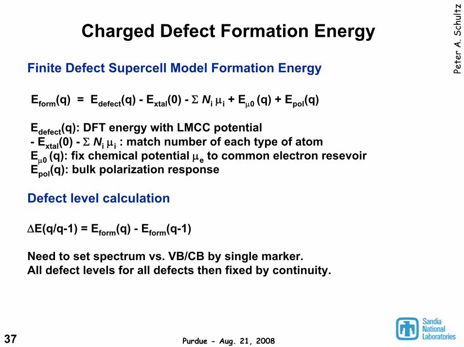
Charged Defect Formation Energy
Finite Defect Supercell Model Formation Energy
Eform(q) = Edefect(q) - Extal(0) - Σ Ni μi + Eμ0 (q) + Epol(q)
Edefect(q): DFT energy with LMCC potential- Extal(0) - Σ Ni μi : match number of each type of atomEμ0 (q): fix chemical potential μe to common electron resevoirEpol(q): bulk polarization response
Defect level calculation
ΔE(q/q-1) = Eform(q) - Eform(q-1)
Need to set spectrum vs. VB/CB by single marker.All defect levels for all defects then fixed by continuity.

38 Purdue - Aug. 21, 2008
Pete
r A
. Sch
ultz
The computational method: DFT/Quest
General purpose DFT code: SeqQuest: http://dft.sandia.gov/QuestMolecules, 1D nanowires, 2D slabs, 3D BulkMetals and insulators (complex k-points)Multiple density functionals: LDA and GGA/PBENorm-conserving pseudopotentials (“semi-local”)Well-converged local orbital (Gaussian-based) basis setForces and stresses, with complete Pulay correctionsAutomatic geometry and cell minimizationFast, small, accurate, powerful --- 100’s atoms on a desktop
Supercomputer DFT on a desktop (plus some parallelism, too)
TDDFT under development (collaboration with Lund, AFRL)Non-equilibrium, electron dynamics, transport ...

39 Purdue - Aug. 21, 2008
Pete
r A
. Sch
ultz
Anatomy of a DFT code(1) Create a guess density: ρ(r) = Σ ρatom(r)
(2) Construct a Hamiltonian, H, over a basis φi : Hij = < φi | H[ρ] | φj >H = T + Vnuc + Vcoul[ρ] + Vxc[ρ]
kinetic nuclear electron-electron electron-electronenergy attraction Coulomb repulsion exchange-correlation
Vnuc = Σ Vatom [R] → N3 Hamiltonian
(3) Solve for wavefunctions ψi :H ψi = εi ψi → N3 eigensolve
(4) Compute new density: ρ(r) = Σ fi | ψi |2
(5) Repeat (2)-(4) until self-consistent
SeqQuest:(1) Map onto a local (Gaussian) orbital basis … small N(2) Reformulate electrostatics … O(N) Hamiltonian

40 Purdue - Aug. 21, 2008
Pete
r A
. Sch
ultz
Both are O(N) !
Analytic local 2 or 3-center: Mesh-based 2-center:
φi
φk
φlVN
φj
(iteration-independent setup) (iteration-dependent scf elements)
Quest: two kinds of matrix elements
φiφ
j
φj

41 Purdue - Aug. 21, 2008
Pete
r A
. Sch
ultz
0
2 0 0
4 0 0
6 0 0
8 0 0
1 0 0 0
0 5 1 0 1 5 2 0 2 5 3 0 3 5 4 0 4 5 5 0
Ru slab: Scaling of SeqQuest calculation
Number of Ru layers
Tim
e (s
ec)
Scaling Ru slab
eigensolver(0001) 1x1 surface vary layer thickness
a0=2.673Å, c/a=1.575 10k/IBZ, ~12Å slab separation
full DZP basis SeqQuest
Actually achieves O(N), and reaches it quickly
42 Purdue - Aug. 21, 2008
Pete
r A
. Sch
ultz
Tim
e (s
ec/a
tom
)
N (# of atoms/unit cell)
4.0
3.5
3.0
2.5
2.0
1.5
1.0
0.5
0.0
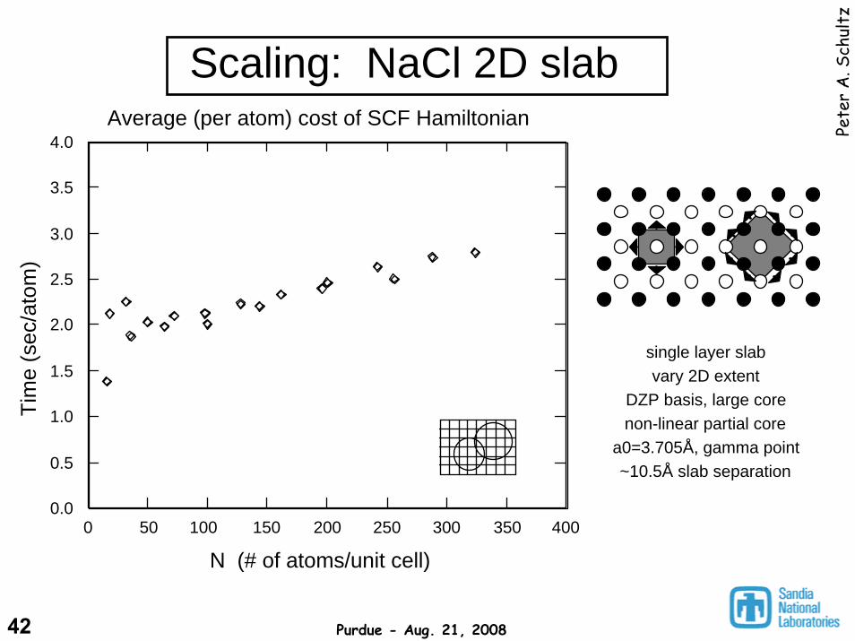
Average (per atom) cost of SCF Hamiltonian
0 100 200 300 40050 150 250 350
Scaling: NaCl 2D slab
single layer slab vary 2D extent
DZP basis, large core non-linear partial core
a0=3.705Å, gamma point ~10.5Å slab separation

43 Purdue - Aug. 21, 2008
Pete
r A
. Sch
ultz
Computational details
Defect supercell calculationsSeqQuest code - periodic, gaussian-basis, pseudopotential code
http://dft.sandia.gov/Quest
LDA and GGA-PBE functionals
Full FDSM (LMCC, chemical potential, DDO, bulk screening)
Calculations ranging from 64-site to 512-site supercells
Converged k-point sampling
Final series: 250-site (5x5x5 fcc cell) with 23 k-points
Fully relaxed atomic positions
Lattice parameter fixed at theoretical value
LDA: 10.20 bohr (5.40 Å)
PBE: 10.34 bohr (5.47 Å)

44 Purdue - Aug. 21, 2008
Pete
r A
. Sch
ultz
The silicon self-interstitial
X (110-split) T (tetrahedral) H (hexagonal)
i[0]? ?

45 Purdue - Aug. 21, 2008
Pete
r A
. Sch
ultz
Si defect structures - DFT/LDA
(2-)
(-)
(0)
(+)
(2+)
i v Os Ss Ns vv Ci Bi Pv Bv
C2v
C2v
C2v
D3d
D3d
D2d
D2dC3v
Td Td
C2v
C2v Td
Td
Td
Td
Td/C3v
D3d
C2h
C2h
C2h
~C2v
C2v
C2v
C1h
C1h
C3v
C1h
C3v
C3v C1h
GGA: E(C2v) < E(D3d) for v(-)
C1
C1

46 Purdue - Aug. 21, 2008
Pete
r A
. Sch
ultz
All formation energies grounded to common electron reservoirFull width of experimental band gap seen in DFT ionization energies
Si: DFT/LDA defect charge transitions
++
+
-
=
++
++
+
++
=- -
0
0 00
0
=
0
+
-0
0
0
+
-
+
-
0
0
-
+
-
v Osi Ss Ns vv Ci Bi Pv Bv4.24.34.44.54.64.74.84.95.05.15.25.35.45.5
(Cxtal )
Ionization potential (eV)+ 0

47 Purdue - Aug. 21, 2008
Pete
r A
. Sch
ultz
Si: Experimental Levels
Experimental record is silent on most important defects!
++
+ +
-
00
=
0
0
0
v Os Ss Ns vv Ci BiiCB1.11.00.90.80.70.60.50.40.30.20.1VB
+
-
+
-
0
+/++0/+
+
0
0
-
+
0
-
Defect level in band gap (eV
)
Pv Bv
0
+
Neededfromtheory
48 Purdue - Aug. 21, 2008
Pete
r A
. Sch
ultz
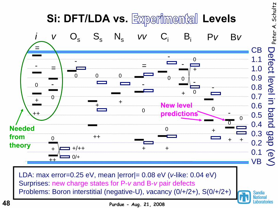
Si: DFT/LDA vs. Experimental Levels
LDA: max error=0.25 eV, mean |error|= 0.08 eV (v-like: 0.04 eV)Surprises: new charge states for P-v and B-v pair defectsProblems: Boron interstitial (negative-U), vacancy (0/+/2+), S(0/+/2+)
New levelpredictions
++
+
-
=
++
++
+
++
- -
0
0
00
0
=
0
v Osi Ss Ns vv Ci
+
Bi
-
0
0
0
CB1.11.00.90.80.70.60.50.40.30.20.1VB
+
-
+
-
0
+/++0/+
+
0
0
-
Pv Bv
Defect level in band gap (eV
)
+
0
-
-0
+
=
Neededfromtheory
0
+

49 Purdue - Aug. 21, 2008
Pete
r A
. Sch
ultz
Si: GGA/PBE vs. Experimental Levels
GGA/PBE improves defect levels with bonding changesPBE max error=0.17 eV, mean |error|=0.08 eV, (v-related: 0.05 eV)New P-v and B-v levels still present
++
+
-=
+++
+
=
- -
0
0 00
0
=
0
v Osi Ss Ns vv Ci Bi
0
0
CB1.11.00.90.80.70.60.50.40.30.20.1VB
+
-
+
-
0
+/++0/+
+
0
0
-
Pv Bv
Defect level in band gap (eV
)
+
0
-
0
+
+/++0/+ -

50 Purdue - Aug. 21, 2008
Pete
r A
. Sch
ultz
P-v and B-v charge states
C1h C1
6e Pv(-) v(2-)
5e Pv(0) v(-)
4e Pv(+) v(0) Bv(-)
3e v(+) Bv(0)
2e v(2+) Bv(+)
v(0) isoelectronic with Pv(+) and Bv(-)
Defect level in band gap (eV
)
CB1.11.00.90.80.70.60.50.40.30.20.1VB
Pv Bv
+
0
-
-0+
-
=
++
+
0
0
v
By analogy to vacancy, expect new charge states isoelectronic to v(0)DFT finds them, they are real, I.e., >0.25 eV (max DFT error) from edgeNew states at midgap -> effective recombination centers

51 Purdue - Aug. 21, 2008
Pete
r A
. Sch
ultzSummary
•Finite Defect Supercell Model - robust computational model of defect- fix boundary conditions (LMCC Poisson solver)- rigorous chemical potential (common electron reservoir)- bulk polarization (bulk screening through modified Jost model)- defect banding (discrete defect occupation scheme)- still needs refinement (e.g., what about strain/elastic effects?)
•Accurate DFT (LDA or PBE) Si defect levels, mean error < 0.1 eV- wide variety of defects - intrinsic, primary, secondary, 1st-row, 2nd-row- top and bottom of band gap- predictive despite band gap problem: new levels in P-v and B-v- evaluated as differences of valid ground state energies, not KS eigenvalues
•Band gap problem?- not in computation of localized defect states from total energy calculations!- However, still have issue of connecting defect level spectrum to band edges- Can we “fix” band gap problem (e.g., w/EXX) without screwing up energies?
Thanks to: Kevin Leung, Ann Mattsson, Art Edwards, Harry Hjalmarson, Renee Van Ginhoven
Contact information: [email protected], http://www.cs.sandia.gov/~paschul

52 Purdue - Aug. 21, 2008
Pete
r A
. Sch
ultzSummary - II
• Beware of Black Boxes (even SeqQuest)!- know your assumptions, control your approximations
“Primer”, Mattsson, et al., MSMSE 13, R1 (2005).- what exactly is your code/simulation doing?
• There is a gap between our tools (DFT codes) and reality (defects)- construction of valid (i.e., quantitative) computational model
• Improvements?- path forward to better (i.e., more accurate) functionals not clear- existing LDA and GGA do very well already
• Questions?
Thanks to:Kevin Leung, Ann Mattsson, Art Edwards, Harry Hjalmarson, Renee Van Ginhoven
Quest DFT code information: http://dft.sandia.gov/Quest
Contact information: [email protected], http://www.cs.sandia.gov/~paschul

53 Purdue - Aug. 21, 2008
Pete
r A
. Sch
ultz
Questions & Answers

54 Purdue - Aug. 21, 2008
Pete
r A
. Sch
ultz
Multiscale ladder for radiation damage
Electrical system responseTe
stin
g
DFT /ATOMISTIC
DEVICE models
CIRCUIT modelsEXPT
EXPT
EXPT
Radiation damage

55 Purdue - Aug. 21, 2008
Pete
r A
. Sch
ultz
Radiation damage and defects
CB
VB
produces defects … and introduces electronic transitions
… and we would like to quantify these transitions
Radiation damage …


![ﻡ 2013 ـﻫ 1435 islamic nation1427@yahoo€¦ · ﻡ 2013 - ـﻫ 1435 islamic_nation1427@yahoo.com ‹ËÜ”÷]](https://static.fdocuments.us/doc/165x107/606289f32474f209fa138569/i-2013-i-1435-islamic-nation1427yahoo-i-2013-i-1435-islamicnation1427yahoocom.jpg)