
Material Safety Data Sheet Material Safety Data Sheet - Agency for

Zarlink Semiconductor Inc.Zarlink, ZL and the Zarlink Semiconductor logo are trademarks of Zarlink Semiconductor Inc.
Copyright 2000-2006, Zarlink Semiconductor Inc. All Rights Reserved.
MT88E46Bellcore Compliant Calling Number
Identification CircuitData Sheet
Features• Compatible with Bellcore GR-30-CORE, SR-
TSV-002476; TIA/EIA-716 and TIA/EIA-777• Pin compatible with MT88E45• Differential input amplifiers with adjustable gains
for Tip/Ring and 4-wire side connections• TIA (Telecommunications Industry Association)
MEI (Multiple Extension Interworking) compatible architecture: CAS (CPE Alerting Signal) detection is selectable between Tip/Ring and 4-wire side
• 4-wire side CAS detection is Bellcore talkoff and talkdown compliant when near end speech is attenuated 8 dB or better, and is close to talkoff compliant even without near end speech attenuation
• Tip/Ring side CAS detection typically meets talkdown condition 1 (the average case)
• 1200 baud Bell 202 and CCITT V.23 FSK demodulation
• Selectable 3-wire FSK data interface (serial bit stream or 1 byte buffer) with facility to monitor stop bit for framing error check
• FSK carrier detect status output• 3 to 5 V ± 10% supply voltage• Uses 3.579545 MHz crystal• Low power CMOS with power down mode
Applications• Bellcore compliant CIDCW (Calling Identity
Delivery on Call Waiting) and CWD (Call Waiting Deluxe) telephones
• CIDCW and CWD telephone adjunct boxes
• Computer Telephony Integrated (CTI) systems
DescriptionThe MT88E46 is a CMOS integrated circuit suitable forreceiving the FSK and CAS signals in North American(Bellcore) CIDCW, CWD and CID (Calling IdentityDelivery) services. It provides an optimal solution for theCIDCW (also known as Type 2) and CWD (Type 2.5)telephone set applications by providing separate input op-amps for Tip/Ring and 4-wire side (receive pair of thetelephone hybrid or speech IC) connections. The Tip/Ringconnection is compatible with TIA’s MEI scheme and canbe used for FSK demodulation and ‘on hook mode’ CASdetection. The 4-wire side connection is for ‘off hookmode’ CAS detection. The CAS detection modes - onhook and off hook - use different algorithms which areoptimized for the CPE states. In ‘off hook mode’ the CASdetector is Bellcore compliant when near end speech isattenuated 8dB or better. ‘On hook mode’ is optimized fortalkdown only and typically meets talkdown condition 1(the average case) without speech attenuation at Tip/Ringsuch as in the on hook state MEI CPE.
Figure 1 - Functional Block Diagram
Anti-AliasFilter
FSKBandpass
FSKDemod
+
-
+
-
Data TimingRecovery
CarrierDetector
2130HzBandpass
2750HzBandpass
ToneDetectionAlgorithm
GS1en
GS1en
Mux
DR
DETBiasGenerator
Oscillator
Control BitDecode
FSKen CASenPWDN
IN1+
IN1-
GS1
IN2+
IN2-
GS2
VREF
OSC1 OSC2 CB0 CB2CB1
DATADCLK
CD
DR/DET
Vdd
VssOn/Off Hook mode
MODE
MODE
FSKen
CASen
CASen
GS1en
PWDN
PWDN
PWDN
Patent pending
November 2006
Ordering Information
MT88E46AS 20 Pin SOIC TubesMT88E46ASR 20 Pin SOIC Tape & ReelMT88E46AS1 20 Pin SOIC* Tubes, Bake &
DrypackMT88E46ASR1 20 Pin SOIC* Tape & Reel,
Bake & Drypack*Pb Free Matte Tin
-40 to +85 °C
MT88E46 Data Sheet
2
Change SummaryChanges from March 2000 Issue to November 2006 Issue.
Figure 2 - Pin Connections
Page Item Change
1 Updated Ordering Information.
Pin Description
Pin # Name Description
1 VREFVoltage Reference (Output). Nominally Vdd/2. It is used to bias the GS1 (Tip/Ring connection) and GS2 (telephone hybrid or speech IC receive pair connection) input op-amps.
2 IN1+ GS1 Op-Amp Non-inverting Input. The op-amp is for connecting the MT88E46 to Tip/Ring.3 IN1- GS1 Op-Amp Inverting Input. The op-amp is for connecting the MT88E46 to Tip/Ring.
4 GS1
Gain Select 1 (Output). This is the output of the GS1 op-amp. The op-amp should be used to connect the MT88E46 to Tip and Ring. The Tip/Ring signal can be amplified or attenuated at GS1 via selection of the feedback resistor between GS1 and IN1-.
FSK demodulation or ‘on hook mode’ CAS detection of the GS1 signal can be selected via the CB1 and CB2 pins. See Tables 1 and 2.
5 Vss Power Supply Ground.6 OSC1 Oscillator Input. Crystal connection. This pin can also be driven directly from an external clock source.
7 OSC2 Oscillator Output. Crystal connection. When OSC1 is driven by an external clock, this pin should be left open circuit.
8 CB0
Control Bit 0 (CMOS Logic Input). This pin is used primarily to select the 3-wire FSK data interface mode. When it is low, interface mode 0 is selected where the FSK bit stream is output directly at the DATA pin. When it is high, interface mode 1 is selected where the FSK byte is stored in a 1 byte buffer which can be read serially by the application’s microcontroller.
The FSK interface is consisted of the DATA, DCLK and DR/DET pins. See the 3 pin descriptions to understand how CB0 affects the FSK interface.
This pin is also used with CB1 and CB2 to put the MT88E46 into a power down state drawing virtually no power supply current. See Tables 1 and 2.
1
2
3
4
5
6
9
10
20
19
18
17
16
15
14
13
VREF
IN1+
IN1-
GS1
Vss
OSC1
DCLK
DATA
IN2+
IN2-
GS2
CB2
CB1
Vdd
CD
NC
MT88E46
7OSC2
8CB0
12
11
IC
DR/DET

3
Data Sheet MT88E46
9 DCLK
3-Wire FSK Interface Data Clock (Schmitt Logic Input/CMOS Logic Output). In interface mode 0 (when the CB0 pin is logic low) this is a CMOS output whose rising edge denotes the nominal mid-point of a bit in the FSK data byte.
In interface mode 1 (when the CB0 pin is logic high) this is a Schmitt trigger input used to shift the FSK data byte out of an on chip buffer to the DATA pin.
10 DATA
3-Wire FSK Interface Data (CMOS Logic Output). Mark frequency corresponds to logical 1. Space frequency corresponds to logical 0.
In interface mode 0 (when the CB0 pin is logic low) the FSK serial bit stream is output to DATA directly.
In interface mode 1 (when the CB0 pin is logic high) the start bit is stripped off, the data byte and the trailing stop bit are stored in a 9 bit buffer. At the end of each word indicated by the DR signal at the DR/DET pin, the microcontroller should shift the byte out to DATA by applying 8 read pulses to the DCLK pin. A 9th DCLK pulse will shift out the trailing stop bit for framing error checking.
11 DR/DET
3-Wire FSK Interface Data Ready/CAS Detect (CMOS Logic Output). Active low. This is a dual purpose pin which indicates the end of an FSK word or the end of CAS.
Data Ready: When FSK demodulation is enabled this pin denotes the end of a word. In both FSK interface modes 0 and 1, it is normally high and goes low for half a bit time at the end of a word. In mode 1 if DCLK starts while DR is low, the first rising edge of the DCLK input will return DR to high. This feature allows an interrupt requested by a low going DR to be cleared upon reading the first DATA bit.
CAS Detect: When CAS detection is enabled, this pin goes low after the end of CAS for 416 µs (nominal) to indicate that CAS has been detected.
12 IC Internal Connection. Must be left open circuit. 13 NC No Connection. This pin is not bonded to the die and is unaffected by external connections.
14 CD
Carrier Detect (CMOS Logic Output). Active low. A logic low indicates that an FSK signal is present. A 10 ms time hysteresis has been provided to allow for momentary signal discontinuity. The demodulated FSK data is ignored until carrier detect has been activated.
15 Vdd Positive Power Supply. A decoupling capacitor should be connected directly across the Vdd and Vss pins.
16 CB1 Control Bit 1 (CMOS Logic Input). Together with CB2 this pin enables FSK demodulation or CAS detection. See Tables 1 and 2.
17 CB2 Control Bit 2 (CMOS Logic Input). Together with CB1 this pin enables FSK demodulation or CAS detection. See Tables 1 and 2.
18 GS2
Gain Select 2 (Output). This is the output of the GS2 op-amp. The op-amp should be used to connect the MT88E46 to the receive pair of the telephone hybrid or speech IC. The signal can be amplified or attenuated at GS2 via selection of the feedback resistor between GS2 and IN2-.
When the application is a telephone adjunct box where there is no hybrid or speech IC, if the GS2 gain with respect to Tip/Ring is to be set to the same as that of GS1, the GS2 op-amp can be connected as a voltage follower to the GS1 op-amp output (see Figure 5).
The GS2 signal is used for ‘off hook mode’ CAS detection only as selected via the CB1 and CB2 pins. See Tables 1 and 2.
19 IN2- GS2 Op-Amp Inverting Input. The op-amp is for connecting the MT88E46 to the receive pair of the telephone hybrid or speech IC.
20 IN2+ GS2 Op-Amp Non-Inverting Input. The op-amp is for connecting the MT88E46 to the receive pair of the telephone hybrid or speech IC.
Pin Description
Pin # Name Description

MT88E46 Data Sheet
4
Control Bit (CB0/1/2) Functionality
Table 1 - CB0/1/2 Function Table
The number of control bits (CB) required to interface the MT88E46 to the microcontroller depends on the functionality ofthe application.
Table 2 -Control Bit Functionality Groups
CB0 CB1 CB2 FSK Interface
Input Op-Amp Function
0/1 1 1 Set by CB0 GS1 FSK Demodulation. DR/DET pin is the DR signal.
0/1 1 0 Set by CB0 GS2
‘Off hook mode’ CAS Detection. DR/DET pin is the DET signal.The off hook mode algorithm is Bellcore talkoff and talkdown compliant when near end speech level is attenuated 8 dB or better. It should be used for the off hook state CPE.
0/1 0 1 Set by CB0 GS1
‘On hook mode’ CAS Detection. DR/DET pin is the DET signal.When the line is in use, a TIA Multiple Extension Interworking (MEI) compatible Type 2 CPE must be able to detect CAS even though the CPE itself is on hook. Since in most telephone designs the hybrid or speech IC is not operational when the CPE itself is on hook, this mode provides Tip Ring CAS detection for the on hook state MEI CPE.
The on hook mode algorithm is optimized for talkdown only and typically meets talkdown condition 1 (the average case) without near end speech attenuation. It must not be used when the CPE itself is off hook. See ‘On Hook Mode CAS Detection’ section in ‘Functional Description’.
1 0 0 Mode 1 -
Power Down. DR/DET pin is logic high.The MT88E46 is disabled and draws virtually no power supply current. Note that the DCLK pin becomes an input pin because FSK interface mode 1 is selected by CB0=1.
0 0 0 Mode 0 - Reserved for factory testing.
Functionality Group Controls Description
FSK, Off Hook mode CAS(Non MEI compatible)
CB2CB0 is connected to Vdd or Vss to select the FSK interface mode.CB1 connected to Vdd.The microcontroller uses CB2 to select between the 2 functions.
FSK, Off Hook mode CAS,On Hook mode CAS
CB1CB2
CB0 is connected to Vdd or Vss to select the FSK interface mode.The microcontroller uses CB1 and CB2 to select between the 3 functions.
FSK (Interface mode 1), Off Hook mode CAS, On Hook mode CAS, Power Down
CB1CB2
CB0 is connected to Vdd to select FSK interface mode 1.The microcontroller uses CB1 and CB2 to select between the 4 functions.
FSK (Interface mode 0), Off Hook mode CAS,On Hook mode CAS, Power Down
CB0CB1CB2
All 3 pins are required.
Data Sheet MT88E46
5
Functional Overview
In the Calling Identity Delivery on Call Waiting (CIDCW)and Call Waiting Deluxe (CWD) services offered byNorth American telephone operating companies, a dualtone known as CAS (CPE Alerting Signal) is sent fromthe central office to notify the near end CPE, which isalready engaged in an established call, that the centraloffice wishes to deliver calling identity information of awaited call. The signalling protocol is specified inBellcore GR-30-CORE, the CPE (Customer PremisesEquipment) requirements in SR-TSV-002476.
In the GR-30-CORE off hook protocol, the central officemutes the far end connection (the other end of theestablished call) just before CAS is transmitted. When thenear end CPE detects the CAS, it mutes the handset andchecks whether there is any parallel off hook CPE. If thereis no parallel off hook CPE, it acknowledges CASreception by sending ACK, which is a predefined DTMFdigit, back to the central office. When the central officereceives ACK, it transmits the calling party information in1200 baud Bell 202 format FSK to the near end CPEwhich then typically displays the information to the user.
When CAS is transmitted from the central office, eventhough the far end has been muted the near end user (theend which is to receive the caller ID information) may bespeaking. Therefore, the CAS must be detected in thepresence of near end speech, noise or music. Failure todetect the CAS and reply with ACK within a definedinterval is known as ‘talkdown’. Talkdown is undesirablebecause the central office will not deliver the callinginformation, hence the quality of the CIDCW or CWDservice will be degraded.
Since CAS can be transmitted anytime during anestablished call, the CAS detector is therefore subjected tospeech, noise or music - which can imitate CAS - fromboth the near end and the far end throughout the call.False detection followed by ACK is known as ‘talkoff’.Talkoff is undesirable because it annoys the far end userby the near end CPE’s sending ACK and because the nearend CPE is muted in anticipation of the FSK signal.
Bellcore has specified talkdown and talkoff immunityperformance requirements in SR-TSV-002476. If the CPEis a telephone, one way to achieve good CAS speechimmunity is to put CAS detection on the receive pair ofthe telephone hybrid or speech IC instead of on Tip andRing. Compared to a Tip/Ring connection, talkdownimmunity improves because the near end speech isattenuated on the hybrid / speech IC receive pair while theCAS level is the same as on Tip/Ring. Talkoff immunity isalso better because the near end speech is attenuated.
In the GR-30-CORE issue 1 off hook protocol, the nearend CPE must not ACK if there is a parallel off hookCPE. Otherwise the ACK will not be detected reliably atthe central office. This restriction is modified by aprotocol known as MEI (Multiple ExtensionInterworking) developed by the TIA(Telecommunications Industry Association) inconjunction with Bellcore. MEI allows a CPE to ACK ifall off hook CPEs are MEI compatible. MEI is describedin the TIA/EIA-777 standard.
MEI introduces the concept of the ACK-Sender and theBackup ACK-Sender.• On a per call basis, the ACK-Sender is the first CPE
to go off hook for the call. It retains its status even if it returned on hook while the line remains in use. The ACK-Sender must give up its status if a Type 3 (Analog Display Services Interface) CPE asserts its ACK-Sender status.
• The Backup ACK-Sender is the CPE to last respond to CAS with an ACK and successfully received FSK data. It retains its status from call to call but must give up its Backup ACK-Sender status when another CPE successfully completes the CAS-ACK-FSK sequence.
When CAS is sent from the central office, all MEIcompatible off hook CPEs detect CAS and go back onhook. After the ACK-Sender detected CAS, it monitorsthe line voltage. When the line voltage has returned to theHIGH state (the voltage when the line is not terminated byany CPE), it goes off hook and sends the ACK. If there isno ACK-Sender because the first CPE to go off hook isnot MEI compatible, the Backup ACK-Sender takes overand sends the ACK. Note that both the ACK-Sender andthe Backup ACK-Sender can be on hook or off hook.
Because it may be the ACK-Sender or Backup ACK-Sender, an MEI compatible on hook state CPE must beable to detect CAS when the line is in use. Additionally,the TIA/EIA-777 standard requires an MEI on hook stateCPE to detect CAS during a call so that it can listen in onthe FSK to keep its call log consistent with the off hookCPEs. However, a CAS detector connected only to thehybrid / speech IC cannot detect CAS when the CPE itselfis on hook because either the hybrid / speech IC is notoperational or the signal level is severely attenuated.Therefore an MEI compatible CPE must be able to detectCAS from Tip/Ring when the CPE is on hook, and be ableto detect CAS from the hybrid / speech IC when the CPEis off hook.The MT88E46 offers an optimal solution which combinesBellcore compliant speech immunity and MEIcompatibility. Two input op-amps allow the MT88E46 tobe connected to both Tip/Ring and to the receive pair ofthe telephone hybrid or speech IC (the 4-wire side). Eachconnection can be differential or single ended. FSK

MT88E46 Data Sheet
6
demodulation is available only at the Tip/Ringconnection. The CAS detector operates in ‘on hook mode’and ‘off hook mode’ using different algorithms optimizedfor the CPE states. On hook mode is available only at theTip/Ring connection, while off hook mode is availableonly at the 4-wire side connection.
The ‘off hook mode’ is Bellcore compliant when the nearend speech is attenuated 8dB or better. It should be usedwhen the CPE is off hook. The ‘on hook mode’ isoptimized for talkdown only and typically meets talkdowncondition 1 (the average case) without near end speechattenuation to provide Tip/Ring CAS detection for the onhook state MEI CPE. It should be used when the CPEitself is on hook but the line is in use.
The FSK demodulator is suitable for both Bell 202 andCCITT V.23 formats transparently, and is compatible withBellcore and TIA standards. The demodulated FSK data iseither output directly (bit stream mode) or stored in a onebyte buffer (buffer mode) which can be shifted out. In thebuffer mode, the stop bit immediately following a byte isalso stored and can be shifted out after the data byte. Thisfacility allows for framing error checking as required inTIA/EIA-777 for the Type 2 CPE. In the bit stream mode,two timing signals are provided. One indicates the bit
sampling instants of the data byte, the other the end of thebyte. A carrier detector indicates the presence of signaland shuts off the data stream when there is no signal.
The entire chip can be put into a power down modeconsuming virtually no power supply current. The inputop-amps, FSK demodulator, CAS detector and theoscillator are all shut off. Furthermore, partial powerdown has been incorporated to minimize the operatingcurrent: when FSK is selected, the CAS detector ispowered down; when CAS is selected, the FSKdemodulator is powered down. The two input op-amps arenot affected by partial power down and will remainoperational regardless of whether FSK or CAS is selected.
Preliminary Off Hook Mode CAS Detector Speech Immunity Performance
Since there is some randomness in speech immunitytesting, and because the telephone hybrid / speech ICdesign will affect the result, the preliminary test results inTables 3 and 4 are provided to illustrate typicalperformances only.
Table 3 - Typical Off Hook Mode Talkoff Immunity Performance
Table 4 -Typical Off Hook Mode Talkdown Immunity Performance
SR-TSV-002476Requirement
Test Result for 0 dB Near End Speech Attenuation using Pre-emphasized
Speech only
Test Result for 0 dB Near End Speech Attenuation
using Pre-emphasized Speech for Near End,
Normal Speech for Far End
Test Result for 6 dB Near End Speech Attenuation
using Pre-emphasized Speech only
Vdd = 5V ± 10%, GS2 gain = 0dB
Condition 1 1 in ≥ 45 hours 1 in 48.0 hours 1 in 96.0 hours 1 in 96.0 hours
Condition 2 1 in ≥ 10 hours 1 in 8.6 hours 1 in 10.1 hours 1 in 16.5 hours
Condition 3 1 in ≥ 35 hours 1 in 37.4 hours 1 in 43.0 hours 1 in 113.1 hours
Vdd = 3V ± 10%, GS2 gain = -4dB
Condition 1 1 in ≥ 45 hours 1 in 32.0 hours TBD 1 in 192.0 hours
Condition 2 1 in ≥ 10 hours 1 in 10.6 hours TBD 1 in 19.9 hours
Condition 3 1 in ≥ 35 hours 1 in 39.8 hours TBD 1 in 123.0 hours
SR-TSV-002476 Requirement
Test Result for 0 dB Near End Speech Attenuation
Test Result for 8 dB Near End Speech Attenuation
Vdd = 5V ± 10% (GS2 gain = 0dB) and 3V ± 10% (GS2 gain = -4dB)
Condition 1 ≥ 99.5% 99.2% 99.9%
Condition 2 ≥ 93.0% 79.6% 93.5%
Condition 3 ≥ 99.5% 97.6% 99.7%
Data Sheet MT88E46
7
In Table 3 (talkoff results) column 3, the result wasobtained using pre-emphasized speech as both the nearend and far end speech sources. It is pessimistic, asrecognized in SR-TSV-002476, because in reality the pre-emphasis originally imparted on the far end speech by thefar end CPE’s microphone would have been equalized bythe subscriber loop, so that at the near end CPE Tip/Ringterminals the far end speech would have no pre-emphasis.Table 3 column 4 shows the result for the same situationas column 3 except that pre-emphasized speech was usedonly as the near end speech source and normal speech wasused as the far end speech source, as allowed in SR-TSV-002476.
In Table 3 column 5 and Table 4 column 4, the MT88E46performance with a telephone hybrid / speech IC wassimulated during testing by attenuating the pre-emphasized near end speech equally at all frequencies.The actual performance will depend on the telephonehybrid / speech IC design.
Functional Description
3 to 5 V Operation
The MT88E46 is designed to operate from a fixed voltagepower supply between 3 and 5 V nominal. A ±10%variation from the nominal voltage is allowed. Its FSKand CAS reject levels are proportional to Vdd. Whenoperated at Vdd equals 3 V ± 10%, to keep the FSK andCAS reject levels as at 5 V ± 10%, and for optimal speechimmunity, the GS1 and GS2 op-amp gains should bereduced from those of 5V. Gains for nominal Vdd’sbetween 3 and 5 V can be obtained by interpolationbetween the 3 V and 5 V values shown in Figure 9.
Input Configuration
The MT88E46 provides an input arrangement comprisedof two op-amps and a bias source (VREF). VREF is a lowimpedance voltage source which is used to bias the op-amp inputs at Vdd/2. The GS1 op-amp (IN1+, IN1-, GS1pins) is for connecting to Tip and Ring. The GS2 op-amp(IN2+, IN2-, GS2 pins) is for connecting to the receivepair of the telephone hybrid or speech IC in the telephoneset application.
Either FSK demodulation or ‘on hook mode’ CASdetection can be selected for the GS1 signal. Only ‘offhook mode’ CAS detection is available for the GS2signal. ‘On hook mode’ CAS detection at the GS1 op-ampis intended for the MEI on hook CPE situation. ‘Off hookmode’ CAS detection at the GS2 op-amp is intended forthe off hook CPE situation.
The feedback resistor connected between IN1- and GS1can be used to adjust the Tip/Ring path input gain, and thefeedback resistor between IN2- and GS2 can be used toadjust the hybrid / speech IC path input gain. When theGS1 op-amp is selected, the GS2 signal is ignored. Whenthe GS2 op-amp is selected, the GS1 signal is ignored.
Either or both op-amps can be configured in the singleended input configuration shown in Figure 3, or in thedifferential input configuration shown in Figure 4.
Figure 3 - Single Ended Input Configuration
Figure 4 - Differential Input ConfigurationIn a telephone adjunct box application where there is nohybrid or speech IC, if the GS2 gain with respect to Tip/Ring is to be set to the same as that of GS1, the GS2 op-amp can be connected as a voltage follower to the GS1op-amp output as shown in Figure 5.
C RININ+
IN-
GS
VREF
Passband Voltage GainAV = RF / RIN
RF
Highpass Corner Frequencyf-3dB= 1/(2πRINC)
C1 R1
C2 R2
R4 R5
R3
IN+
IN-
GS
VREF
Differential Input AmplifierC1 = C2R2 = R1 (For unity gain R3= R1)R4 = (R3R5) / (R3 + R5)Passband Voltage Gain(AVdiff) = R3/R1
Input Impedance
(ZINdiff) = 2 R12 + (1/ωC1)2
Highpass Corner Frequencyf-3dB= 1/(2πR1C1)

MT88E46 Data Sheet
8
Figure 5 - GS2 Op-Amp Connected as GS1 Voltage Follower
CAS Detection
When CAS detection is selected, the dual purpose DR/DET pin is the DET output signal. DET goes lowmomentarily (416 µsec nominal) after the end of CAS toindicate that CAS has been detected, as shown in Figure13. The CAS detector operates in ‘off hook mode’ or ‘onhook mode’ as selected by the CB1 and CB2 pins (seeTable 1). ‘On hook mode’ and ‘off hook mode’ usedifferent algorithms optimized for the CPE states.
Normally DET goes low after the end of CAS. However,because of interference from speech or music, DET maygo low before the end of CAS. The on hook and off hookmode algorithms ensure that DET will occur no earlierthan tDET1 after the beginning of CAS (see Figure 13).
Similarly, speech interference can cause DET to go lowlater than tDET2 after the end of CAS (see Figure 13). Inoff hook mode, the detection algorithm ensures that DETwill occur no later than 35ms after the end of CAS evenwith speech interference, as required in TIA/EIA-777. Inon hook mode, although the detection algorithm does notlimit the detection delay from the end of CAS, talkdowntypically meets the SR-TSV-002476 talkdown condition 1(the average case) when only the detections which occurfrom the beginning of CAS to 35 ms after the end of CASare counted.
Off Hook Mode CAS Detection
The ‘off hook mode’ is Bellcore talkdown and talkoffcompliant when the near end speech is attenuated 8dB orbetter, such as provided by the telephone hybrid or speechIC. When near end speech is not attenuated, such as froma parallel off hook CPE or when the application is atelephone adjunct box, talkoff is close to compliant whiletalkdown is close to condition 1 (the average case). Thismode is intended for the off hook CPE situation and isavailable at the GS2 (4-wire side) input op-amp only.
On Hook Mode CAS Detection
The ‘on hook mode’ is optimized for talkdown only. Ittypically meets talkdown condition 1 without near endspeech attenuation. It is intended for the MEI on hookCPE situation and must not be used when the CPE itself isoff hook. The input is the GS1(Tip/Ring) op-amp becausein most CPE designs, to detect CAS when the CPE itselfis on hook, the signal must come from the Tip/Ringconnection since either the telephone hybrid / speech IC isnot operational or the 4-wire side signal level is severelyattenuated.
In the MEI protocol, the ACK-Sender and Backup ACK-Sender can be on hook or off hook. Therefore, if the onhook state CPE is the ACK-Sender or the Backup ACK-Sender, it must be able to detect CAS when the line is inuse. Additionally, an on hook state MEI CPE must be ableto detect CAS during a call so that it can listen in on theFSK to keep its call log consistent with the off hookCPEs, as required in TIA/EIA-777.
The MT88E46 on hook mode algorithm has beenoptimized for talkdown because of the way the MEIprotocol works. In MEI, the following events (describedin TIA/EIA-777) occur when CAS is detected:• Each off hook CPE shall proceed to the on hook
state not earlier than 25 ms and no later than 60 ms after the end of CAS as measured on Tip/Ring. (The 25 ms delay is necessary to prevent the on hook transition from corrupting the CAS for other CPEs that may not have completely qualified the signal. The additional 35 ms that defines the 60 ms upper limit allows for variation in CAS detection delay.)
• After detecting a line HIGH state (the line voltage when the line is not terminated by any CPE), the ACK-Sender shall go off hook. The ACK-Sender shall allow the line to remain in the HIGH state for at least 5 ms but not more than 8ms. If no line HIGH state is detected within 100ms after going on hook, all previously off hook CPE shall return to the off hook state.
• Following a CAS the Backup ACK-Sender shall monitor the line for a line HIGH state lasting a minimum of 15 ms. Once this condition has been detected, the Backup ACK-Sender shall immediately become the ACK-Sender, go off hook no later than 20 ms after the start of the line HIGH state, complete the CAS-ACK handshake, and remain as ACK-Sender for the remainder of the call. This situation may happen if the designated ACK-Sender is not MEI compliant.
• An MEI compliant CPE that is not the designated ACK-Sender or the Backup ACK-Sender but which is off hook at the time of the CAS, shall monitor the line for a line HIGH state lasting a minimum of 30 ms. Once this condition has been detected, the
IN2+
IN2-
GS1
GS2
GS1 op-amp configured as in Figure 3 or 4

Data Sheet MT88E46
9
CPE shall immediately become the ACK-Sender, go off hook no later than 35 ms after the start of the line HIGH state, complete the CAS-ACK handshake, and remain as ACK-Sender for the duration of the call. This situation can happen if the designated ACK-Sender and the Backup ACK-Sender are not MEI compliant.
• After going off hook the ACK-Sender shall begin transmission of the ACK no earlier than 30 ms and no later than 40 ms after the leading edge of the line HIGH voltage transition.
After the ACK-Sender or Backup ACK-Sender detectedCAS, it must monitor the line for the line HIGH state,which can happen only if all off hook CPEs also detectedCAS. Hence if the ACK-Sender or Backup ACK-Senderis an on hook CPE, even if it falsely detected CAS, talkoffcan occur only if all off hook CPEs also falsely detectedCAS. Thus in the situation where the ACK-Sender orBackup ACK-Sender is an on hook CPE using theMT88E46 on hook mode detection algorithm, talkoffprotection is provided by the off hook CPEs. The on hookmode has been optimized to be more talkdown immune sothat in this situation the on hook CPE will be successful infulfilling its ACK-Sender or Backup ACK-Senderresponsibility.
FSK Demodulation
The FSK demodulator is compatible with Bellcore SR-TSV-002476, TIA/EIA-716 and TIA/EIA-777 standards.It is capable of both Bell 202 and CCITT V.23 formatstransparently. FSK demodulation is available at the GS1input op-amp only.
FSK Data Interface
The MT88E46 provides a powerful dual mode 3-wireinterface so that the data bytes in the demodulated FSK bitstream can be extracted without the need either for anexternal UART or for the CPE’s microcontroller toperform the function in software.
The interface is specifically designed for the 1200 baudrate and is consisted of 3 signals: DATA, DCLK (DataClock) and DR (Data Ready). DATA is an output pin.DCLK is an input output pin. DR uses the dual purposeoutput pin DR/DET. When FSK is selected it is the DRsignal.
Two FSK interface modes (modes 0 and 1) are selectablevia the CB0 pin. In mode 0, the FSK bit stream is outputdirectly. In mode 1, the data byte and the trailing stop bitare stored in a 9 bit buffer. If mode 1 is used, the CB0 pincan be connected to Vdd. If mode 0 is used and full chip
power down is not required, the CB0 pin can be connectedto Vss.
In Bellcore’s off hook protocol, a Type 2 CPE shouldrestore the voicepath within 50 ms after the end of theFSK signal. Due to noise, end of carrier detection is notalways reliable. The TIA/EIA-777 standard requires theCPE to detect the end of FSK when any one of thefollowing occurs:• absence of carrier signal or,• more than five framing errors (trailing stop bit a 0
instead of a 1) have been detected in the FSK message or,
• more than 150 ms of continuous mark signal or space signal has been detected.
FSK Data Interface Mode 0 - Bit Stream Mode
This mode is selected when the CB0 pin is low. In thismode the FSK data is output directly to the DATA pin.DCLK and DR are timing signal outputs (see Figure 14).
For each received stop and start bit sequence, theMT88E46 outputs a fixed frequency clock string of 8pulses at the DCLK pin. Each DCLK rising edge occurs inthe middle of a DATA bit of the FSK byte. DCLK is notgenerated for the start and stop bits. Consequently, DCLKwill clock only valid data into a peripheral device such asa serial to parallel shift register or into a microcontroller.The MT88E46 also outputs an end of word pulse DR(Data Ready). DR goes low for half a nominal bit time atthe beginning of the trailing stop bit. It can be used tointerrupt a microcontroller or cause a serial to parallelconverter to parallel load its data into the microcontroller.If a shift register is not used, DCLK and DATA mayoccupy 2 bits of a microcontroller’s input port. Themicrocontroller polls the input port and saves the DATAbit when DCLK changes from low to high. When DR goeslow, the word may then be assembled from the last 8saved bits.
Since the DR rising edge occurs in the middle of thetrailing stop bit, it can be used to read the stop bit to checkfor framing error. Alternatively, at the DR falling edge themicrocontroller can set a timer for a 1/2400 secondtimeout and read the stop bit at DATA when the timertimes out.
DATA may also be connected to a personal computer’sserial communication port after conversion from CMOSto RS-232 voltage levels.
FSK Data Interface Mode 1 - Buffer Mode
This mode is selected when the CB0 pin is high. In thismode the received byte is stored on chip. At the end of a
MT88E46 Data Sheet
10
byte DR goes low to indicate that a new byte has becomeavailable. The microcontroller applies pulses at the DCLKinput pin to read the register contents serially out of theDATA pin (see Figure 15).
Internal to the MT88E46, the start bit is stripped off, thedata bits and the trailing stop bit are sampled and stored.Midway through the stop bit, the 8 data bits and the stopbit are parallel loaded into a 9 bit shift register and DRgoes low. The register’s contents are shifted out to theDATA pin on the supplied DCLK’s rising edges in theorder they were received. The last bit must be shifted outand DCLK returned to low before the next DR. DCLKmust be low for tDDS before DR goes low and remain lowfor tDDH after DR has gone low (see Figure 15 and ‘ACElectrical Characteristics - Mode 1 FSK Data InterfaceTiming’).
If DCLK begins while DR is low, DR will return to highupon the first DCLK rising edge. If DR interrupts amicrocontroller then this feature allows the interrupt to becleared by the first read pulse. Otherwise DR is low forhalf a nominal bit time (1/2400 sec).
Reading the stop bit allows the software to check forframing errors. When framing error is not checked themicrocontroller only needs to send 8 DCLK pulses to shiftthe data byte out.
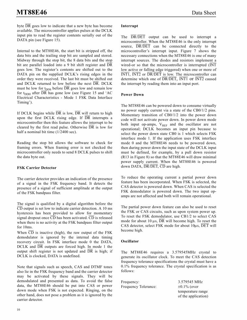
FSK Carrier Detector
The carrier detector provides an indication of the presenceof a signal in the FSK frequency band. It detects thepresence of a signal of sufficient amplitude at the outputof the FSK bandpass filter.
The signal is qualified by a digital algorithm before theCD output is set low to indicate carrier detection. A 10 mshysteresis has been provided to allow for momentarysignal dropout once CD has been activated. CD is releasedwhen there is no activity at the FSK bandpass filter outputfor 10ms. When CD is inactive (high), the raw output of the FSKdemodulator is ignored by the internal data timingrecovery circuit. In FSK interface mode 0 the DATA,DCLK and DR outputs are forced high. In mode 1 theoutput shift register is not updated and DR is high; ifDCLK is clocked, DATA is undefined.
Note that signals such as speech, CAS and DTMF tonesalso lie in the FSK frequency band and the carrier detectormay be activated by these signals. They will bedemodulated and presented as data. To avoid the falsedata, the MT88E46 should be put into CAS or powerdown mode when FSK is not expected. Ringing, on theother hand, does not pose a problem as it is ignored by thecarrier detector.
Interrupt
The DR/DET output can be used to interrupt amicrocontroller. When the MT88E46 is the only interruptsource, DR/DET can be connected directly to themicrocontroller’s interrupt input. Figure 7 shows thenecessary connections when the MT88E46 is one of manyinterrupt sources. The diodes and resistors implement awired-or so that the microcontroller is interrupted (INTlow active or falling edge triggered) when one or more ofINT1, INT2 or DR/DET is low. The microcontroller candetermine which one of DR/DET, INT1 or INT2 causedthe interrupt by reading them into an input port.
Power Down
The MT88E46 can be powered down to consume virtuallyno power supply current via a state of the CB0/1/2 pins.Momentary transition of CB0/1/2 into the power downcode will not activate power down. In power down modeboth input op-amps, VREF and the oscillator are notoperational; DCLK becomes an input pin because toselect the power down state CB0 is 1 which selects FSKinterface mode 1. If the application uses FSK interfacemode 0 and the MT88E46 needs to be powered down,then during power down the input state of the DCLK inputmust be defined, for example, by a pull down resistor(R13 in Figure 8) so that the MT88E46 will draw minimalpower supply current. When the MT88E46 is powereddown DATA, DR/DET, CD are high.
To reduce the operating current a partial power downfeature has been incorporated. When FSK is selected, theCAS detector is powered down. When CAS is selected theFSK demodulator is powered down. The two input op-amps are not affected and both will remain operational.
The partial power down feature can also be used to resetthe FSK or CAS circuits, such as upon system power up.To reset the FSK demodulator, use CB1/2 to select CASmode for about 10 µs, DR will become high. To reset theCAS detector, select FSK mode for about 10µs, DET willbecome high.
Oscillator
The MT88E46 requires a 3.579545MHz crystal togenerate its oscillator clock. To meet the CAS detectionfrequency tolerance specifications the crystal must have a0.1% frequency tolerance. The crystal specification is asfollows:
Frequency: 3.579545 MHzFrequency Tolerance: ±0.1% (over
temperature rangeof the application)

Data Sheet MT88E46
11
Resonance Mode: ParallelLoad Capacitance: 18pFMaximum Series Resistance: 150 ΩMaximum Drive Level: 2 mWe.g. CTS MP036S
Alternatively an external clock source can be used. Inwhich case the OSC1 pin should be driven directly from aCMOS buffer and the OSC2 pin left open.
For 5V±10% applications any number of MT88E46’s canbe connected as shown in Figure 6 so that only one crystalis required.
Figure 6 - Common Crystal Connection
OSC1 OSC2 OSC1 OSC2 OSC1 OSC2
3.579545 MHz
MT88E46 MT88E46 MT88E46
to the next MT88E46
(For 5V±10% applications only)
Figure 7 - Application Circuit: Multiple Interrupt Sources
Interrupt Source 1
INT1(Open Drain)
Interrupt Source 2
INT2(CMOS)
MT88E46
Vdd
R2
DR/DET(CMOS)
INT (input)
Microcontroller
Input Port Bit
R1 can be opened and D1 shorted if the microcontroller does not read the INT1 pin.
D1
Vdd
R1

MT88E46 Data Sheet
12
Figure 8 - Application Circuit: MEI Compatible Type 2 Telephone
Unless stated otherwise, resistors are 1%, 0.1Watt; capacitors are 5%, 6.3V.
For 1000Vrms, 60Hz isolation from Tip to Earth and Ring to Earth:R1,R2 430K, 0.5W, 5%, 475V minimum C1,C2 2n2, 1332V minimum
(e.g. IRC type GS-3)
If the 1000Vrms is handled by other methods then this circuit has to meet the FCC Part 68 Type B Ringer requirements:R1,R2 432K, 0.1W, 1%, 56V minimum C1,C2 2n2, 212V minimum
Common to both sets of R1,R2 and C1,C2:R3,R4 34KR8, R9 464KR13 100K, 20%. Required only if both FSK interface mode 0 and power down features are used.C3,C4 2n2C5 100n, 20%D1-D4 Diodes. 1N4148 or equivalentXtal 3.579545MHz, 0.1% crystal
Vdd = 5V±10% 3V±10% Vdd = 5V±10% 3V±10%GS1 Gain 0dB -4.0dB (preliminary) GS2 Gain 0dB -4.0dB (preliminary)R5 53K6 34K0 R10 53K6 34K0R6 60K4 38K3 R11 60K4 38K3R7 464K 294K R12 464K 294K
In a telephone adjunct box application where there is no hybrid or speech IC, if the GS2 gain with respect to Tip/Ring is to be set to the same as GS1, the GS2 op-amp can be connected as a voltage follower to the GS1 output as shown in Figure 5.
VREF
IN1+
IN1-
GS1
Vss
OSC1
DCLK
DATA
IN2+
IN2-
GS2
CB2
CB1
Vdd
CD
NC
MT88E46
OSC2
CB0
IC
DR/DET
Telephone
Tx+
Tx-
Rx+
Rx-
TIP
RING
Microphone
Speaker
TIP
RING
R1
R2
R3
R4
R5 R6
D1
D2
D3
D4
R7
R8
R9
R10R11
R12
C1
C2
C3
C4
Xtal
R13
C5
Hybrid or
(FSK Interface Mode 1 selected)
R13 is required only if both FSK interface mode 0 and power down features are used.
± 10% power= To Microcontroller
= From Microcontroller Vss
Speech IC(Symbolic)
supply
C5 should be connecteddirectly across the Vddand Vss pins.

13
Data Sheet MT88E46
Figure 9 - GS1 and GS2 Gain Ratios as a Function of Nominal Vdd
Gain Setting Resistor Calculation for Nominal Vdd between 3 and 5V
• For the desired nominal Vdd, use Figure 9 to calculate approximate Av.• For the GS1 op-amp, start with the 0dB gain setting resistor values of R50dB, R60dB and R70dB. In Figure 8 they
are 53K6, 60K4 and 464K respectively. Keep R1, R2, R3, R4, C1, C2 as in Figure 8 to keep the input highpass filter corner frequency constant for all gain settings.
• For the desired Av:R7Av = R70dB x Av Scaled for desired gain. Choose the closest standard 1% resistor
value as R7Av. Calculate Av_actual as R7Av/R70dB.R5Av= R50dB x Av_actual Scaled for good common mode range. Choose the closest
standard 1% resistor as R5Av.1/R6Av= 1/R5Av-1/R7Av Calculate R6Av so that R5Av = R6Av || R7Av. Choose the closest
standard 1% resistor as R6Av.• Repeat for R10, R11 and R12 for the GS2 op-amp.
Example:
• For the 3 V gain of -4.0 dB, Av = 0.63095.• R7-4dB = 0.63095 x 464K = 292.76K. The closest standard 1% resistor is 294K.
Av_actual is 294K/464K = 0.63362 or -3.96 dB.• R5-4dB = 0.63362 x 53K6 = 33.96K. The closest standard 1% resistor is 34K0.• 1/R6-4dB = 1/34.0K - 1/294K = 1/38.45K. The closest standard 1% resistor is 38K3.
3.0 3.5 4.0 4.5 5.0
Nominal Vdd (Volts)
0.60
0.65
0.70
0.75
0.80
0.85
0.90
0.95
1.00
Gai
n R
atio
0.63095
1.000
PRELIMINARY

MT88E46 Data Sheet
14
* Exceeding these values may cause permanent damage. Functional operation under these conditions is not implied.** Under normal operating conditions voltage on any pin except supplies can be minimum Vss-1V to maximum Vdd+1V for an input current limited to less than 200 µA.
‡Typical figures are at 25°C and are for design aid only: not guaranteed and not subject to production testing.
Absolute Maximum Ratings* - Voltages are with respect to Vss unless otherwise stated
Parameter Sym. Min. Max. Units
1 Supply voltage with respect to Vss Vdd -0.3 6 V
2 Voltage on any pin other than supplies ** VPIN Vss-0.3 Vdd+0.3 V
3 Current at any pin other than supplies IPIN - 10 mA
4 Storage Temperature TST -65 150 oC
Recommended Operating Conditions - Voltages are with respect to ground (Vss) unless otherwise stated
Characteristics Sym. Min. Typ.‡ Max. Units
1 Power Supplies Vdd 2.7 - 5.5 V
2 Clock Frequency fOSC - 3.579545 - MHz
3 Tolerance on Clock Frequency ∆fOSC -0.1 - +0.1 %
4 Operating Temperature TOP -40 - 85 oC
DC Electrical Characteristics†
Characteristics Sym. Min. Typ.‡ Max. Units Test Conditions
1SUPPLY
Power Down Mode Supply Current IDDQ - 0.1 15 µA
All inputs are at Vdd/Vss except for oscillator pins, outputs unloaded.CB0/1/2 = 100
2
Operating SupplyCurrentVdd = 5V ±10%Vdd = 3V ±10%
IDD --
4.32.7
84.5
mAmA
All inputs are at Vdd/Vss except for oscillator pins. No analog input, outputs unloaded.
3 Power Consumption PO - - 44 mW
4DCLK
Schmitt Input High Threshold VT+
0.48*Vdd - 0.68*Vdd V
Schmitt Input Low Threshold VT-
0.28*Vdd - 0.48*Vdd V
5 Schmitt Hysteresis VHYS 0.2 - - V
6CB0CB1CB2
CMOS Input High Voltage VIH 0.7*Vdd - Vdd V
CMOS Input Low Voltage VIL Vss - 0.3*Vdd V
7
DCLKDATA
DR/DETCD
Output High Source Current IOH 0.8 - - mA VOH=0.9*Vdd
15
Data Sheet MT88E46
†DC Electrical Characteristics are over recommended operating conditions, unless otherwise stated.‡Typical figures are at 25°C and are for design aid only: not guaranteed and not subject to production testing.
†AC Electrical Characteristics are over recommended operating conditions, unless otherwise stated.‡Typical figures are at 25°C and are for design aid only: not guaranteed and not subject to production testing.
*Notes:1. OSC1 frequency at 3.579545 MHz ± 0.1%.2. Tip/Ring or 4-wire side input signal level. Signal level is per tone.
dBm = decibels above or below a reference power of 1 mW into 600 ohms. 0 dBm = 0.7746Vrms. dBV = decibels above or below a reference voltage of 1 Vrms. 0 dBV = 1 Vrms.
3. ‘On Hook mode’: GS1 op-amp configured to 0 dB gain for Vdd=5V±10%, -4 dB (preliminary) for Vdd=3V±10%.4. ‘Off Hook mode’: GS2 op-amp configured to 0 dB gain for Vdd=5V±10%, -4 dB (preliminary) for Vdd=3V±10%.5. When the signal level difference between the upper and lower tones is within the twist limits.6. Test condition is both tones have the same amplitude.
8
DCLK DATA
DR/DETCD
Output Low Sink Current IOL 2 - - mA VOL=0.1*Vdd
9
IN1+IN1-IN2+IN2-
Input Current
IIN1 - - 1 µA VIN=Vdd to Vss
DCLKCB0CB1CB2
IIN2 - - 10 µA VIN=Vdd to Vss
10VREF
Output Voltage VREF0.5Vdd
-0.1 - 0.5Vdd+0.1 V No Load
11 Output Resistance RREF - - 2 kΩ
AC Electrical Characteristics† - CAS Detection
Characteristics Sym. Min. Typ.‡ Max. Unit Notes*
1 Upper Tone Frequency fH 2736.2 2750 2763.8 Hz 1
2 Lower Tone Frequency fL 2119.3 2130 2140.7 Hz 1
3 Accept Signal Level (per tone) -32-34.22 - -14
-16.22dBmdBV 1, 2, 3, 4, 5
4 ‘Off Hook mode’ Reject Signal Level (per tone) - - -45
-47.22dBmdBV 1, 2, 4, 6
5 Twist: 20 log (V2130Hz/V2750Hz) -6 - +6 dB 1, 3, 4
6 ‘Off Hook mode’ Accept CAS Duration 75 80 85 ms
7 ‘On Hook mode’ Accept CAS Duration 75 - - ms
8 CAS Detection Delay from Start of CAS tDET1 60 - - ms See Figure 13
9 CAS Detection Delay from End of CAS - No speech tDET2 - - 15 ms See Figure 13
10 CAS Detection Indicator Pulse Width tDW 415 416 417 µs See Figure 13
DC Electrical Characteristics† (continued)
Characteristics Sym. Min. Typ.‡ Max. Units Test Conditions
MT88E46 Data Sheet
16
†AC Electrical Characteristics are over recommended operating conditions, unless otherwise stated.‡Typical figures are at 25°C and are for design aid only: not guaranteed and not subject to production testing.
*Notes:1. Tip/Ring input signal level.
dBm = decibels above or below a reference power of 1 mW into 600 ohms. 0 dBm = 0.7746Vrms. dBV = decibels above or below a reference voltage of 1 Vrms. 0dBV = 1 Vrms.
2. GS1 op-amp configured to 0 dB gain for Vdd=5V±10%, -4 dB (preliminary) for Vdd=3V±10%.3. Both mark and space have the same amplitude. 4. Band limited random noise (300-3400 Hz). Present when FSK signal is present.
†Electrical characteristics are over recommended operating conditions, unless otherwise stated.
AC Electrical Characteristics† - FSK Demodulation
Characteristics Sym. Min. Typ.‡ Max. Units Notes*
1 Accept Signal Level-40
-37.7810.0
--6.45-4.23476
dBVdBm
mVrms1, 2
2 Bell 202 Format Reject Signal Level - --50.46-48.24
3
dBVdBm
mVrms1, 2, 3
3 Transmission Rate 1188 1200 1212 baud
4
Mark and Space FrequenciesBell 202 1 (Mark)Bell 202 0 (Space)
CCITT V.23 1 (Mark)CCITT V.23 0 (Space)
11882178
1280.52068.5
12002200
13002100
12122222
1319.52131.5
HzHz
HzHz
5 Twist: 20 log (VMARK/VSPACE) -6 - +10 dB 2
6 Signal to Noise Ratio SNRFSK 20 - - dB 2, 3, 4
7 Input FSK to CD low delay tCP - - 25 ms See Figures 16, 17
8 Input FSK to CD high delay tCA 10 - - ms See Figures 16, 17
9 CD Time Hysteresis 10 - - ms
Electrical Characteristics† - Gain Setting Amplifiers
Characteristics Sym. Min. Max. Units Test Conditions
1 Input Leakage Current IIN - 1 µA Vss ≤ VIN ≤ Vdd
2 Input Resistance RIN 10 - MΩ
3 Input Offset Voltage VOS - 25 mV
4 Power Supply Rejection Ratio PSRR 30 - dB 1kHz ripple on Vdd
5 Common Mode Rejection Ratio CMRR 40 - dB VCMmin ≤ VIN ≤ VCMmax
6 DC Open Loop Voltage Gain AVOL 40 - dB
7 Unity Gain Bandwidth fC 0.3 - MHz
8 Output Voltage Swing VO 0.5 Vdd-0.7 V Load ≥ 100kΩ
9 Capacitive Load (GS1,GS2) CL - 50 pF
10 Resistive Load (GS1,GS2) RL 100 - kΩ
11 Common Mode Range Voltage VCM 1.0 Vdd-1.0 V

17
Data Sheet MT88E46
†AC Electrical Characteristics are over recommended operating conditions, unless otherwise stated.‡Typical figures are at 25°C and are for design aid only: not guaranteed and not subject to production testing.
*Notes:1. OSC1 at 3.579545 MHz ± 0.1%.2. FSK input data at 1200 ± 12 baud.3. Function of signal condition.
†AC Electrical Characteristics are over recommended operating conditions unless otherwise stated.
†AC Electrical Characteristics are over recommended operating conditions unless otherwise stated.
AC Electrical Characteristics† - Mode 0 FSK Data Interface Timing
Characteristics Sym. Min. Typ.‡ Max. Units Notes*
1
DR
Rise time tRR - - 200 ns into 50 pF loadSee Figure 11
2 Fall time tRF - - 200 ns into 50 pF loadSee Figure 11
3 Low time tRL 415 416 417 µs 1. See Figs. 11, 14, 15
4DATA
Rate 1188 1200 1212 baud 2
5 Input FSK to DATA delay tIDD - 1 5 ms See Figure 14
6
DATADCLK
Rise time tR - - 200 ns into 50 pF loadSee Figure 10
7 Fall time tF - - 200 ns into 50 pF loadSee Figure 10
8 DATA to DCLK delay tDCD 6 416 - µs 1, 2, 3See Figure 10
9 DCLK to DATA delay tCDD 6 416 - µs 1, 2, 3See Figure 10
10
DCLK
Frequency fDCLK0 1201.6 1202.8 1204 Hz 1. See Figure 14
11 High time tCH 415 416 417 µs 1. See Figures 10, 14
12 Low time tCL 415 416 417 µs 1. See Figures 10, 14
13 DCLKDR DCLK to DR delay tCRD 415 416 417 µs 1. See Figure 14
AC Electrical Characteristics† - Mode 1 FSK Data Interface Timing
Characteristics Sym. Min. Max. Units Notes
1
DCLK
Frequency fDCLK1 - 1 MHz See Figure 15
2 Duty cycle 30 70 %
3 Rise time tR1 - 100 ns See Figure 12
4 DCLKDR
DCLK low set up to DR tDDS 500 - ns See Figure 15
5 DCLK low hold time after DR tDDH 500 - ns See Figure 15
AC Electrical Characteristics† - General Timing
Characteristics Sym. Min. Max. Units Notes
1OSC2
Power-up time tPU - 50 ms See Figures 16, 17
2 Power-down time tPD - 10 ms See Figure 16

MT88E46 Data Sheet
18
Figure 10 - DATA and DCLK Mode 0 Output Timing
Figure 11 - DR Output Timing
Figure 12 - DCLK Mode 1 Input Timing
AC Electrical Characteristics - Timing Parameter Measurement Voltage Levels
Characteristics Sym. Level Units Notes
1 CMOS Threshold Voltage VCT 0.5*Vdd V
2 Rise/Fall Threshold Voltage High VHM 0.7*Vdd V
3 Rise/Fall Threshold Voltage Low VLM 0.3*Vdd V
DATA
DCLK
tR
tDCD tCDD
tR
tF
tCL tCH
tF
VHM
VLMVCT
VHM
VLM
VCT
tRF tRR
tRL
DRVHM
VLM
VCT
DCLK
tR1
VHM
VLM

19
Data Sheet MT88E46
Figure 13 - CAS Detection Timing
Figure 14 - FSK Data Interface Timing - Mode 0
Figure 15 - FSK Data Interface Timing - Mode 1
CAS
DET
tDET2
tDW = 416µs nominal(Output)
tDET1
See ‘AC Electrical Characteristics - CAS Detection’ for tDET1 and tDET2 values.
Note: The relationship between DATA bit boundary and DCLK is symbolic only. In reality, the DATA bit boundary will jitter with respect to theDCLK falling edges.
TIP/RING
DATA(Output)
DCLK(Output)
DR(Output)
b7 b0 b1 b2 b3 b4 b5 b6 b7 b0 b1 b2 b3 b4 b5 b6 b7 b0 b1 b2 b3 b4 b5
b7 b0 b1 b2 b3 b4 b5 b6 b7 b0 b1 b2 b3 b4 b5 b6 b7 b0 b1 b2 b3b6
stop
start
stop
start
stop
start
stop
start
stop
start
stop
start
tIDD
tCRD
tRL
tCLtCH 1/fDCLK0
Demodulated Data(Internal Signal)
DCLK (Data Clock)(Schmitt Input)
DR (Data Ready)(Output)
stop start stop0 1 2 3 4 5 6 77
Word N Word N+1
DATA(Output)
5
Word NWord N-1
1/fDCLK1
tRL
>tDDH
The DCLK input must be low before and after DR falling edge.Note 1: DCLK occurs during DR low and returns DR to high.Note 2: DCLK occurs after DR, so DR is low for half a nominal bit time. Note 3: When framing error (trailing stop bit a 0 instead of a 1) is not checked, the microcontroller only needs to send 8 DCLK pulses toshift the byte out.
>tDDS
43210 6 7 stopstop7 0
Note 1
Note 2
Note 3
MT88E46 Data Sheet
20
Figure 16 - Application Timing: Bellcore On-Hook Data Transmission Associated with Ringing, e.g. Calling Number Delivery, Calling Name Delivery
Notes:This on-hook case application is included because a CIDCW CPE must also be capable of receiving on-hook data transmission (with ringing) from the central office. 1) PWDN and FSKen are internal signals decoded from CB0/1/2. 2) The CPE designer may choose to enable the MT88E46 only after the end of ringing to conserve power in a battery operated CPE. CD is not
activated by ringing. 3) The microcontroller in the CPE powers down the MT88E46 after CD has become inactive.4) The microcontroller times out if CD is not activated.5) The DR/DET output pin is the DR signal when FSK is selected.
1st Ring 2nd RingCh. seizure Mark Data
A C D E F
..101010.. Data
Note 2 Note 3 Note 2 Note 4
tCAtCP
B
TIP/RING
PWDN
OSC2
FSKen
CD
DR
DCLK
DATA
A = 2sec typicalB = 250-500msC = 250msD = 150msE = feature specificMax C+D+E = 2.9 to 3.7secF ≥ 200ms
tPDtPU(Note 1)
(Note 1)
(Note 5)

21
Data Sheet MT88E46
Figure 17 - Application Timing: Bellcore Off-Hook Data Transmission, e.g. CIDCWNotes:1) In a CPE where AC power is not available, the designer may choose to switch over to line power when the CPE goes off-hook and use battery
power while on-hook. The CPE must also be CID (on-hook) capable because a CIDCW CPE includes CID functionality. 2) Non-FSK signals such as CAS, speech and DTMF tones are in the same frequency band as FSK. They will be demodulated and give false data.
Therefore the MT88E46 should be taken out of FSK mode when FSK is not expected. 3) If the CPE is the ACK-Sender, the MT88E46 may be put into FSK mode right after ACK has been sent. If the CPE is not the ACK-Sender, the
MT88E46 should be put into FSK mode at 30 ms (min ACK delay) + 55 ms (min ACK duration) = 85 ms after the line HIGH transition. In that case the FSK carrier detector may be activated by the ACK if both the ACK delay and the ACK duration are at maximum. TR-NWT-000575 specifies that ACK = DTMF ‘D’ for non-ADSI CPE, ‘A’ for ADSI CPE.
4) The MT88E46 should be taken out of FSK mode when CD has become inactive, or when more than 5 framing errors have been detected in the message, or when more than 150 ms of continuous Mark or Space has been detected.
5) In an unsuccessful attempt where the central office does not send the FSK signal, the CPE should unmute the handset and enable the keypad after interval D has expired.
6) PWDN, Off Hook CASen and FSKen are internal signals decoded from CB0/1/2.7) The DR/DET output pin is the DET signal when CAS detection is selected, the DR signal when FSK is selected.
CPE goes off-hook
CAS ACK
CPE sends
CPE mutes handset, disables keypad
Mark Data
CPE unmutes handsetand enables keypad
tDET2
tDW tCP tCA
Data
A C E F GB D
Note 1
Note 3 Note 4
Note 5
TIP/RING
PWDN
FSKen
OSC2
DET
CD
DR
DCLK
DATA
A = 75-85msB = 0-100msC = 55-65msD = 0-500msE = 58-75msF = feature specificG ≤ 50ms
tPU
(Note 6)
(Note 6)
(Note 7)
Note 2
(Note 7)
Off Hook CASen(Note 6)
and performs MEI check (See TIA/EIA-777)
Speech
25ms
30-40ms

www.zarlink.com
Information relating to products and services furnished herein by Zarlink Semiconductor Inc. or its subsidiaries (collectively “Zarlink”) is believed to be reliable.However, Zarlink assumes no liability for errors that may appear in this publication, or for liability otherwise arising from the application or use of any suchinformation, product or service or for any infringement of patents or other intellectual property rights owned by third parties which may result from such application oruse. Neither the supply of such information or purchase of product or service conveys any license, either express or implied, under patents or other intellectualproperty rights owned by Zarlink or licensed from third parties by Zarlink, whatsoever. Purchasers of products are also hereby notified that the use of product incertain ways or in combination with Zarlink, or non-Zarlink furnished goods or services may infringe patents or other intellectual property rights owned by Zarlink.
This publication is issued to provide information only and (unless agreed by Zarlink in writing) may not be used, applied or reproduced for any purpose nor form partof any order or contract nor to be regarded as a representation relating to the products or services concerned. The products, their specifications, services and otherinformation appearing in this publication are subject to change by Zarlink without notice. No warranty or guarantee express or implied is made regarding thecapability, performance or suitability of any product or service. Information concerning possible methods of use is provided as a guide only and does not constituteany guarantee that such methods of use will be satisfactory in a specific piece of equipment. It is the user’s responsibility to fully determine the performance andsuitability of any equipment using such information and to ensure that any publication or data used is up to date and has not been superseded. Manufacturing doesnot necessarily include testing of all functions or parameters. These products are not suitable for use in any medical products whose failure to perform may result insignificant injury or death to the user. All products and materials are sold and services provided subject to Zarlink’s conditions of sale which are available on request.
Purchase of Zarlink’s I2C components conveys a licence under the Philips I2C Patent rights to use these components in and I2C System, provided that the systemconforms to the I2C Standard Specification as defined by Philips.
Zarlink, ZL, the Zarlink Semiconductor logo and the Legerity logo and combinations thereof, VoiceEdge, VoicePort, SLAC, ISLIC, ISLAC and VoicePath aretrademarks of Zarlink Semiconductor Inc.
TECHNICAL DOCUMENTATION - NOT FOR RESALE
For more information about all Zarlink productsvisit our Web Site at