MR1A16A, 128K x 16-Bit 3.3-V Asynchronous Magnetoresistive ... · PDF fileThe MR1A16A is a...
22
© Freescale Semiconductor, Inc., 2007. All rights reserved. Freescale Semiconductor Data Sheet Document Number: MR1A16A Rev. 3, 11/2007 Introduction The MR1A16A is a 2,097,152-bit magnetoresistive random access memory (MRAM) device organized as 131,072 words of 16 bits. The MR1A16A is equipped with chip enable (E ), write enable (W ), and output enable (G ) pins, allowing for significant system design flexibility without bus contention. Because the MR1A16A has separate byte-enable controls (LB and UB ), individual bytes can be written and read. MRAM is a nonvolatile memory technology that protects data in the event of power loss and does not require periodic refreshing. The MR1A16A is the ideal memory solution for applications that must permanently store and retrieve critical data quickly. The MR1A16A is available in a 400-mil, 44-lead plastic small-outline TSOP type-II package with an industry-standard center power and ground SRAM pinout. The MR1A16A is available in Commercial (0°C to 70°C), Industrial (-40°C to 85°C) and Extended (-40°C to 105°C) ambient temperature ranges. Features • Single 3.3-V power supply • Commercial temperature range (0°C to 70°C), Industrial temperature range (-40°C to 85°C) and Extended temperature range (-40°C to 105°C) • Symmetrical high-speed read and write with fast access time (35 ns) • Flexible data bus control — 8 bit or 16 bit access • Equal address and chip-enable access times • Automatic data protection with low-voltage inhibit circuitry to prevent writes on power loss • All inputs and outputs are transistor-transistor logic (TTL) compatible • Fully static operation • Full nonvolatile operation with 20 years minimum data retention 128K x 16-Bit 3.3-V Asynchronous Magnetoresistive RAM MR1A16A 44-TSOP Case 924A-02
Transcript of MR1A16A, 128K x 16-Bit 3.3-V Asynchronous Magnetoresistive ... · PDF fileThe MR1A16A is a...

Freescale SemiconductorData Sheet
Document Number: MR1A16ARev. 3, 11/2007
128K x 16-Bit 3.3-V Asynchronous Magnetoresistive RAM
MR1A16A
44-TSOPCase 924A-02
Introduction
The MR1A16A is a 2,097,152-bit magnetoresistive random access memory (MRAM) device organized as 131,072 words of 16 bits. The MR1A16A is equipped with chip enable (E), write enable (W), and output enable (G) pins, allowing for significant system design flexibility without bus contention. Because the MR1A16A has separate byte-enable controls (LB and UB), individual bytes can be written and read.
MRAM is a nonvolatile memory technology that protects data in the event of power loss and does not require periodic refreshing. The MR1A16A is the ideal memory solution for applications that must permanently store and retrieve critical data quickly.
The MR1A16A is available in a 400-mil, 44-lead plastic small-outline TSOP type-II package with an industry-standard center power and ground SRAM pinout.
The MR1A16A is available in Commercial (0°C to 70°C), Industrial (-40°C to 85°C) and Extended (-40°C to 105°C) ambient temperature ranges.
Features
• Single 3.3-V power supply
• Commercial temperature range (0°C to 70°C), Industrial temperature range (-40°C to 85°C) and Extended temperature range (-40°C to 105°C)
• Symmetrical high-speed read and write with fast access time (35 ns)
• Flexible data bus control — 8 bit or 16 bit access
• Equal address and chip-enable access times
• Automatic data protection with low-voltage inhibit circuitry to prevent writes on power loss
• All inputs and outputs are transistor-transistor logic (TTL) compatible
• Fully static operation
• Full nonvolatile operation with 20 years minimum data retention
© Freescale Semiconductor, Inc., 2007. All rights reserved.

Device Pin Assignment
Figure 1. Block Diagram
Device Pin Assignment
Figure 2. MR1A16A in 44-Pin TSOP Type II Package
UPPER BYTE OUTPUT ENABLE
LOWER BYTE OUTPUT ENABLE
COLUMNDECODER
ROWDECODER
128K x 16BIT
MEMORYARRAY
FINALWRITE
DRIVERS
SENSEAMPS
UPPER BYTE WRITE ENABLE
LOWER BYTE WRITE ENABLE
OUTPUTENABLEBUFFER
CHIPENABLEBUFFER
WRITEENABLEBUFFER
BYTEENABLEBUFFER
ADDRESSBUFFERS
UPPERBYTE
OUTPUTBUFFER
LOWERBYTE
OUTPUTBUFFER
UPPERBYTE
WRITEDRIVER
LOWERBYTE
WRITEDRIVER
DQL[7:0]
DQU[15:8]
G
E
W
UB
LB
8
9
8
8
8
8
16
16
17
A[16:0]
8
8
8
8
UB
LB
4443
4241
40
3938
3736
3534
3332
3130
2928
2726
2524
23
12
34
5
67
89
1011
1213
1415
1617
1819
2021
22
A16A15
A14G
UB
LBDQU15
DQU14DQU13
DQU12VSS
VDD
DQU11
DQU10DQU9
DQU8NC
VDD
A13
A12A11
A10
A0A1
A2A3
A4
EDQL0
DQL1DQL2
DQL3VDD
VSS
DQL4
DQL5DQL6
DQL7W
A5A6
A7A8
A9
Table 1. Pin Functions
Signal Name Function
A Address input
E Chip enable
W Write enable
G Output enable
UB Upper byte select
LB Lower byte select
DQL Data I/O, lower byte
DQU Data I/O, upper byte
VDD Power supply
VSS Ground
NC Do not connect this pin
MR1A16A Data Sheet, Rev. 3
2 Freescale Semiconductor
Electrical Specifications
Electrical Specifications
Absolute Maximum Ratings
This device contains circuitry to protect the inputs against damage caused by high static voltages or electric fields; however, it is advised that normal precautions be taken to avoid application of any voltage greater than maximum rated voltages to these high-impedance (Hi-Z) circuits.
The device also contains protection against external magnetic fields. Precautions should be taken to avoid application of any magnetic field more intense than the maximum field intensity specified in the maximum ratings.
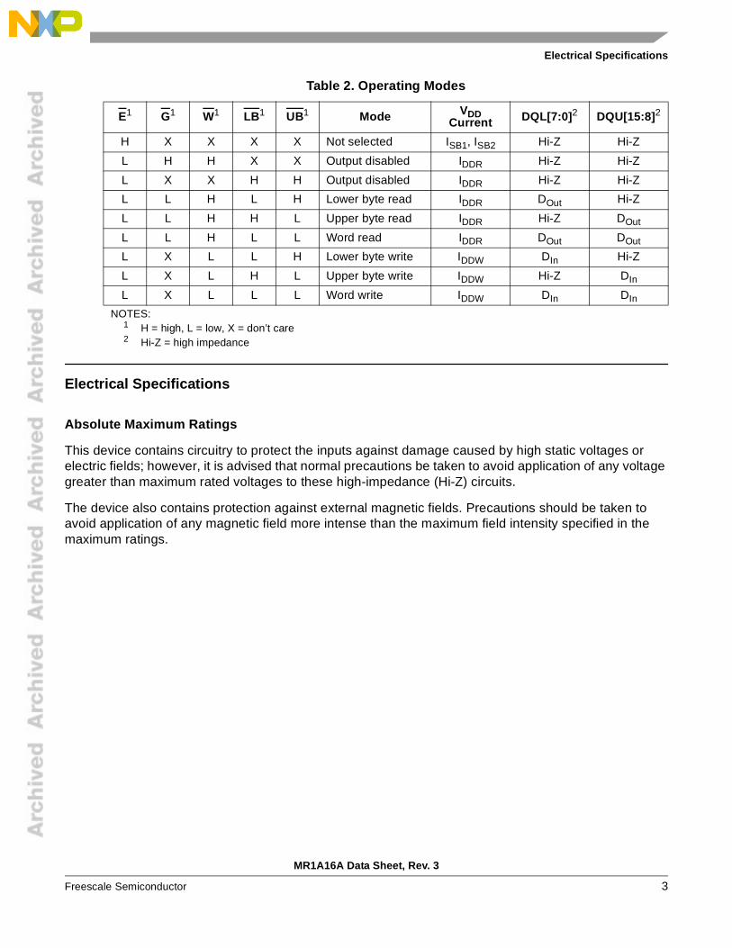
Table 2. Operating Modes
E1 G1 W1 LB1 UB1 Mode VDD Current DQL[7:0]2 DQU[15:8]2
H X X X X Not selected ISB1, ISB2 Hi-Z Hi-Z
L H H X X Output disabled IDDR Hi-Z Hi-Z
L X X H H Output disabled IDDR Hi-Z Hi-Z
L L H L H Lower byte read IDDR DOut Hi-Z
L L H H L Upper byte read IDDR Hi-Z DOut
L L H L L Word read IDDR DOut DOut
L X L L H Lower byte write IDDW DIn Hi-Z
L X L H L Upper byte write IDDW Hi-Z DIn
L X L L L Word write IDDW DIn DIn
NOTES:1 H = high, L = low, X = don’t care2 Hi-Z = high impedance
MR1A16A Data Sheet, Rev. 3
Freescale Semiconductor 3

Electrical Specifications
Table 3. Absolute Maximum Ratings1
Parameter Symbol Value Unit
Supply voltage2 VDD –0.5 to 4.0 V
Voltage on any pin2 VIn –0.5 to VDD + 0.5 V
Output current per pin IOut ±20 mA
Package power dissipation3 PD 0.600 W
Temperature under bias MR1A16AYS35 (Commercial)MR1A16ACYS35 (Industrial)MR1A16AVYS35 (Extended)
TBias–10 to 85–45 to 95–45 to 110
°C
Storage temperature Tstg –55 to 150 °C
Lead temperature during solder (3 minute max) TLead 260 °C
Maximum magnetic field during write MR1A16AYS35 (Commercial)MR1A16ACYS35 (Industrial)MR1A16AVYS35 (Extended)
Hmax_write152525
Oe
Maximum magnetic field during read or standby Hmax_read 100 Oe
NOTES:1 Permanent device damage may occur if absolute maximum ratings are exceeded. Functional operation
should be restricted to recommended operating conditions. Exposure to excessive voltages or magnetic fieldscould affect device reliability.
2 All voltages are referenced to VSS.3 Power dissipation capability depends on package characteristics and use environment.
Table 4. Operating Conditions
Parameter Symbol Min Typ Max Unit
Power supply voltage VDD 3.01 3.3 3.6 V
Write inhibit voltage VWI 2.5 2.7 3.01 V
Input high voltage VIH 2.2 —VDD + 0.32 V
Input low voltage VIL –0.53 — 0.8 V
Operating temperatureMR1A16AYS35 (Commercial)MR1A16ACYS35 (Industrial)MR1A16AVYS35 (Extended)
TA0
-40-40
7085105
°C
NOTES:1 After power up or if VDD falls below VWI, a waiting period of 2 ms must be observed, and E and W
must remain high for 2 ms. Memory is designed to prevent writing for all input pin conditions if VDDfalls below minimum VWI.
2 VIH (max) = VDD + 0.3 Vdc; VIH (max) = VDD + 2.0 Vac (pulse width ≤ 10 ns) for I ≤ 20.0 mA.3 VIL (min) = –0.5 Vdc; VIL (min) = –2.0 Vac (pulse width ≤ 10 ns) for I ≤ 20.0 mA.
MR1A16A Data Sheet, Rev. 3
4 Freescale Semiconductor
Electrical Specifications
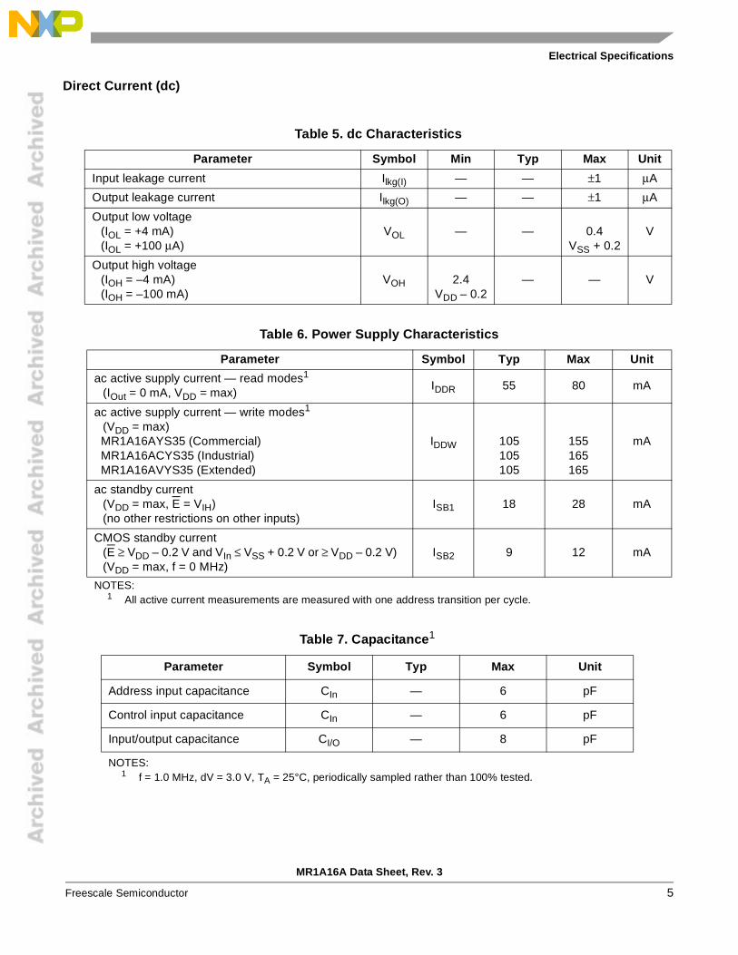
Direct Current (dc)
Table 5. dc Characteristics
Parameter Symbol Min Typ Max Unit
Input leakage current Ilkg(I) — — ±1 μA
Output leakage current Ilkg(O) — — ±1 μA
Output low voltage(IOL = +4 mA)(IOL = +100 μA)
VOL — — 0.4 VSS + 0.2
V
Output high voltage (IOH = –4 mA)(IOH = –100 mA)
VOH 2.4 VDD – 0.2
— — V
Table 6. Power Supply Characteristics
Parameter Symbol Typ Max Unit
ac active supply current — read modes1
(IOut = 0 mA, VDD = max)IDDR 55 80 mA
ac active supply current — write modes1
(VDD = max)MR1A16AYS35 (Commercial)MR1A16ACYS35 (Industrial)MR1A16AVYS35 (Extended)
IDDW 105105105
155165165
mA
ac standby current(VDD = max, E = VIH)(no other restrictions on other inputs)
ISB1 18 28 mA
CMOS standby current (E ≥ VDD – 0.2 V and VIn ≤ VSS + 0.2 V or ≥ VDD – 0.2 V) (VDD = max, f = 0 MHz)
ISB2 9 12 mA
NOTES:1 All active current measurements are measured with one address transition per cycle.
Table 7. Capacitance1
Parameter Symbol Typ Max Unit
Address input capacitance CIn — 6 pF
Control input capacitance CIn — 6 pF
Input/output capacitance CI/O — 8 pF
NOTES:1 f = 1.0 MHz, dV = 3.0 V, TA = 25°C, periodically sampled rather than 100% tested.
MR1A16A Data Sheet, Rev. 3
Freescale Semiconductor 5

Electrical Specifications
Figure 3. Output Load for ac Test
Table 8. ac Measurement Conditions
Parameter Value
Logic input timing measurement reference level 1.5 V
Logic output timing measurement reference level 1.5 V
Logic input pulse levels 0 or 3.0 V
Input rise/fall time 2 ns
Output load for low and high impedance parameters See Figure 3A
Output load for all other timing parameters See Figure 3B
A B
OUTPUT
RL = 50 Ω
VL = 1.5 V
ZD = 50 Ω
OUTPUT
600 Ω
725 Ω
5 pF
+3.3 V
MR1A16A Data Sheet, Rev. 3
6 Freescale Semiconductor
Electrical Specifications
This page is intentionally blank.
MR1A16A Data Sheet, Rev. 3
Freescale Semiconductor 7
Timing Specifications
Timing Specifications
Read Mode
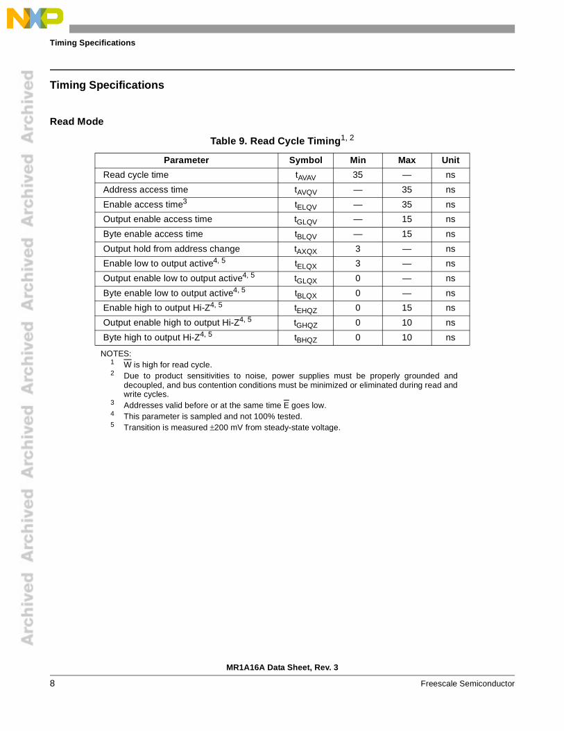
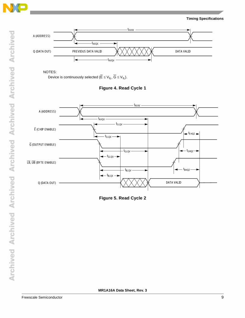
Table 9. Read Cycle Timing1, 2
Parameter Symbol Min Max Unit
Read cycle time tAVAV 35 — ns
Address access time tAVQV — 35 ns
Enable access time3 tELQV — 35 ns
Output enable access time tGLQV — 15 ns
Byte enable access time tBLQV — 15 ns
Output hold from address change tAXQX 3 — ns
Enable low to output active4, 5 tELQX 3 — ns
Output enable low to output active4, 5 tGLQX 0 — ns
Byte enable low to output active4, 5 tBLQX 0 — ns
Enable high to output Hi-Z4, 5 tEHQZ 0 15 ns
Output enable high to output Hi-Z4, 5 tGHQZ 0 10 ns
Byte high to output Hi-Z4, 5 tBHQZ 0 10 ns
NOTES:1 W is high for read cycle.2 Due to product sensitivities to noise, power supplies must be properly grounded and
decoupled, and bus contention conditions must be minimized or eliminated during read andwrite cycles.
3 Addresses valid before or at the same time E goes low.4 This parameter is sampled and not 100% tested.5 Transition is measured ±200 mV from steady-state voltage.
MR1A16A Data Sheet, Rev. 3
8 Freescale Semiconductor
Timing Specifications
Figure 4. Read Cycle 1
Figure 5. Read Cycle 2
tAVAV
tAXQX
tAVQV
DATA VALIDPREVIOUS DATA VALIDQ (DATA OUT)
A (ADDRESS)
NOTES:Device is continuously selected (E ≤ VIL, G ≤ VIL).
tAVAV
tAVQV
A (ADDRESS)
tELQX
tGLQV
DATA VALID
E (CHIP ENABLE)
G (OUTPUT ENABLE)
LB, UB (BYTE ENABLE)
Q (DATA OUT)
tELQV
tGLQX
tBLQV
tBLQX
tBHQZ
tGHQZ
tEHQZ
MR1A16A Data Sheet, Rev. 3
Freescale Semiconductor 9

Timing Specifications
Write Mode
Table 10. Write Cycle Timing 1 (W Controlled)1, 2, 3, 4, 5
Parameter Symbol Min Max Unit
Write cycle time6 tAVAV 35 — ns
Address set-up time tAVWL 0 — ns
Address valid to end of write (G high) tAVWH 18 — ns
Address valid to end of write (G low) tAVWH 20 — ns
Write pulse width (G high)tWLWH tWLEH
15 — ns
Write pulse width (G low)tWLWH tWLEH
15 — ns
Data valid to end of write tDVWH 10 — ns
Data hold time tWHDX 0 — ns
Write low to data Hi-Z7, 8, 9 tWLQZ 0 12 ns
Write high to output active7, 8, 9 tWHQX 3 — ns
Write recovery time tWHAX 12 — ns
NOTES:1 A write occurs during the overlap of E low and W low.2 Due to product sensitivities to noise, power supplies must be properly grounded and decoupled and
bus contention conditions must be minimized or eliminated during read and write cycles.3 If G goes low at the same time or after W goes low, the output will remain in a high-impedance state.4 After W, E, or UB/LB has been brought high, the signal must remain in steady-state high for a minimum
of 2 ns.5 The minimum time between E being asserted low in one cycle to E being asserted low in a subsequent
cycle is the same as the minimum cycle time allowed for the device.6 All write cycle timings are referenced from the last valid address to the first transition address.7 This parameter is sampled and not 100% tested.8 Transition is measured ±200 mV from steady-state voltage.9 At any given voltage or temperature, tWLQZ max < tWHQX min.
MR1A16A Data Sheet, Rev. 3
10 Freescale Semiconductor

Timing Specifications
Figure 6. Write Cycle 1 (W Controlled)
tAVAV
tAVWH
A (ADDRESS)
tWLEH
DATA VALID
E (CHIP ENABLE)
W (WRITE ENABLE)
LB, UB (BYTE ENABLE)
Q (DATA OUT)
tDVWH
tWLQZ
tWHDX
D (DATA IN)
tWHAX
Hi-ZHi-Z
tAVWL
tWLWH
tWHQX
MR1A16A Data Sheet, Rev. 3
Freescale Semiconductor 11
Timing Specifications
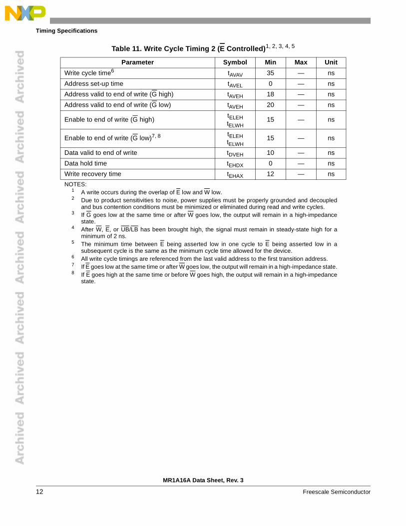
Table 11. Write Cycle Timing 2 (E Controlled)1, 2, 3, 4, 5
Parameter Symbol Min Max Unit
Write cycle time6 tAVAV 35 — ns
Address set-up time tAVEL 0 — ns
Address valid to end of write (G high) tAVEH 18 — ns
Address valid to end of write (G low) tAVEH 20 — ns
Enable to end of write (G high)tELEH tELWH
15 — ns
Enable to end of write (G low)7, 8 tELEH tELWH
15 — ns
Data valid to end of write tDVEH 10 — ns
Data hold time tEHDX 0 — ns
Write recovery time tEHAX 12 — ns
NOTES:1 A write occurs during the overlap of E low and W low.2 Due to product sensitivities to noise, power supplies must be properly grounded and decoupled
and bus contention conditions must be minimized or eliminated during read and write cycles.3 If G goes low at the same time or after W goes low, the output will remain in a high-impedance
state.4 After W, E, or UB/LB has been brought high, the signal must remain in steady-state high for a
minimum of 2 ns.5 The minimum time between E being asserted low in one cycle to E being asserted low in a
subsequent cycle is the same as the minimum cycle time allowed for the device.6 All write cycle timings are referenced from the last valid address to the first transition address.7 If E goes low at the same time or after W goes low, the output will remain in a high-impedance state.8 If E goes high at the same time or before W goes high, the output will remain in a high-impedance
state.
MR1A16A Data Sheet, Rev. 3
12 Freescale Semiconductor

Timing Specifications
Figure 7. Write Cycle 2 (E Controlled)
tAVAV
tAVEH
A (ADDRESS)
DATA VALID
E (CHIP ENABLE)
W (WRITE ENABLE)
LB, UB (BYTE ENABLE)
Q (DATA OUT)
D (DATA IN)
tEHAX
Hi-Z
tELEH
tDVEH
tAVEL tELWH
tEHDX
MR1A16A Data Sheet, Rev. 3
Freescale Semiconductor 13
Timing Specifications
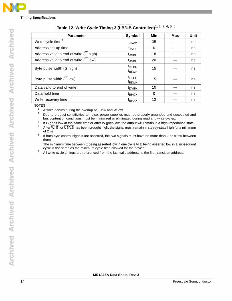
Table 12. Write Cycle Timing 3 (LB/UB Controlled)1, 2, 3, 4, 5, 6
Parameter Symbol Min Max Unit
Write cycle time7 tAVAV 35 — ns
Address set-up time tAVBL 0 — ns
Address valid to end of write (G high) tAVBH 18 — ns
Address valid to end of write (G low) tAVBH 20 — ns
Byte pulse width (G high)tBLEH tBLWH
15 — ns
Byte pulse width (G low)tBLEH tBLWH
15 — ns
Data valid to end of write tDVBH 10 — ns
Data hold time tBHDX 0 — ns
Write recovery time tBHAX 12 — ns
NOTES:1 A write occurs during the overlap of E low and W low.2 Due to product sensitivities to noise, power supplies must be properly grounded and decoupled and
bus contention conditions must be minimized or eliminated during read and write cycles.3 If G goes low at the same time or after W goes low, the output will remain in a high-impedance state.4 After W, E, or UB/LB has been brought high, the signal must remain in steady-state high for a minimum
of 2 ns.5 If both byte control signals are asserted, the two signals must have no more than 2 ns skew between
them.6 The minimum time between E being asserted low in one cycle to E being asserted low in a subsequent
cycle is the same as the minimum cycle time allowed for the device.7 All write cycle timings are referenced from the last valid address to the first transition address.
MR1A16A Data Sheet, Rev. 3
14 Freescale Semiconductor
Timing Specifications
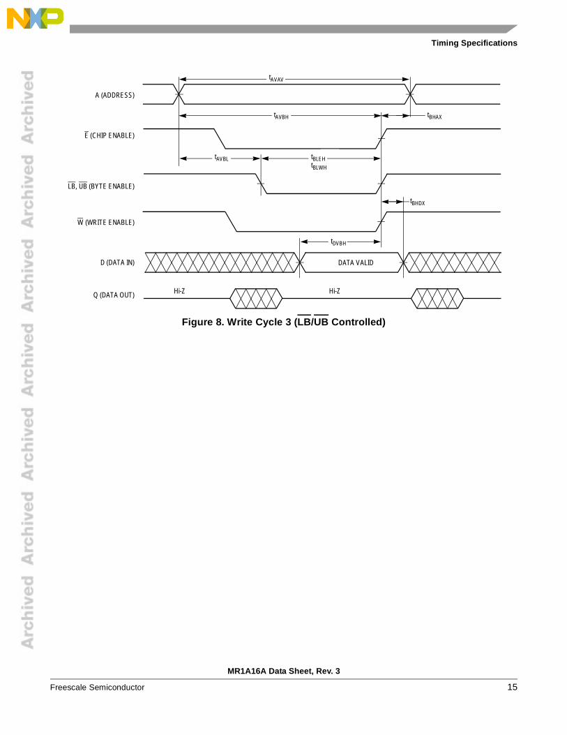
Figure 8. Write Cycle 3 (LB/UB Controlled)
tAVAV
tBHAX
A (ADDRESS)
DATA VALID
E (CHIP ENABLE)
W (WRITE ENABLE)
LB, UB (BYTE ENABLE)
Q (DATA OUT)
D (DATA IN)
Hi-ZHi-Z
tAVBL tBLEHtBLWH
tBHDX
tDVBH
tAVBH
MR1A16A Data Sheet, Rev. 3
Freescale Semiconductor 15

Ordering Information
Ordering Information
This product is available in Commercial, Industrial, and Extended temperature versions.
Freescale's semiconductor products can be classified into the following tiers: “Commercial”, “Industrial” and “Extended.” A product should only be used in applications appropriate to its tier as shown below. For questions, please contact a Freescale sales representative.
• Commercial — Typically 5 year applications - personal computers, PDA's, portable telecom products, consumer electronics, etc.
• Industrial, Extended — Typically 10 year applications - installed telecom equipment, workstations, servers, etc. These products can also be used in Commercial applications.
Part Numbering System
Package Information
Table 13. Package Information
Device Pin Count
Package Type Designator Case No. Document No. RoHS
Compliant
MR1A16A 44TSOPType II
YS 924A-02 98ASS23673W True
(Order by Full Part Number)
MR
Freescale MRAM Memory PrefixDensity Code (0 = 1 Mb, 1 = 2 Mb,
Timing Set (35 = 35 ns)
Revision (A = rev 1)I/O Configuration (08 = 8 bits, 16 = 16 bits)
1 16A A V YS 35
Memory Type (A = async, S = sync)2 = 4 Mb, 4 = 16 Mb)
Package Type (YS = TSOP II)Operating Temperature Range(Missing = 0°C to 70°C,C = -40°C to 85°C, V = -40°C to 105°C)
MR1A16A Data Sheet, Rev. 3
16 Freescale Semiconductor
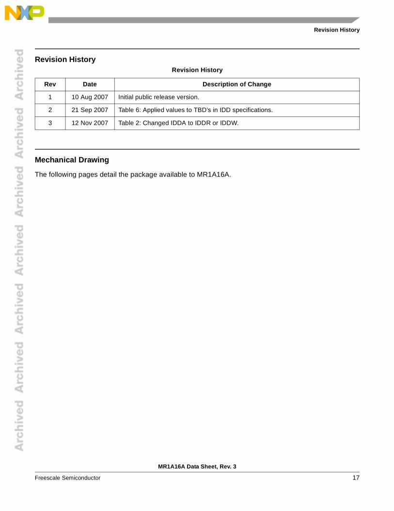
Revision History
Revision History
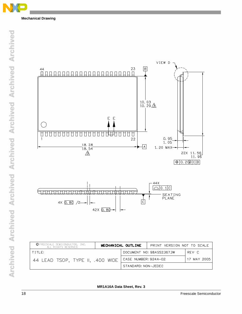
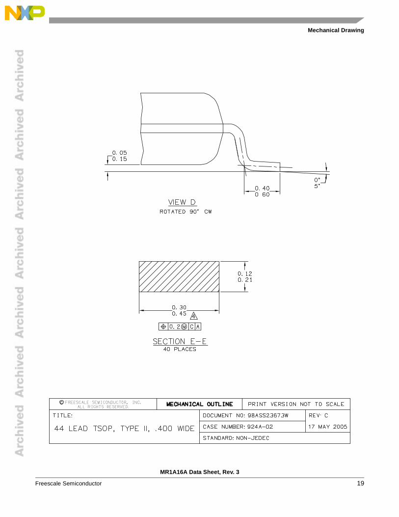
Mechanical Drawing
The following pages detail the package available to MR1A16A.
Revision History
Rev Date Description of Change
1 10 Aug 2007 Initial public release version.
2 21 Sep 2007 Table 6: Applied values to TBD’s in IDD specifications.
3 12 Nov 2007 Table 2: Changed IDDA to IDDR or IDDW.
MR1A16A Data Sheet, Rev. 3
Freescale Semiconductor 17
Mechanical Drawing
MR1A16A Data Sheet, Rev. 3
18 Freescale Semiconductor
Mechanical Drawing
MR1A16A Data Sheet, Rev. 3
Freescale Semiconductor 19

Mechanical Drawing
MR1A16A Data Sheet, Rev. 3
20 Freescale Semiconductor
Mechanical Drawing
MR1A16A Data Sheet, Rev. 3
Freescale Semiconductor 21
MR1A16ARev. 3, 11/2007
How to Reach Us:
USA/Europe/Locations not listed:Freescale Semiconductor Literature DistributionP.O. Box 5405, Denver, Colorado 802171-800-521-6274 or 480-768-2130
Japan:Freescale Semiconductor Japan Ltd.SPS, Technical Information Center3-20-1, Minami-AzabuMinato-kuTokyo 106-8573, Japan81-3-3440-3569
Asia/Pacific:Freescale Semiconductor H.K. Ltd.2 Dai King StreetTai Po Industrial EstateTai Po, N.T. Hong Kong852-26668334
Learn More:For more information about Freescale Semiconductor products, please visithttp://www.freescale.com
Information in this document is provided solely to enable system and software implementers to use
Freescale Semiconductor products. There are no express or implied copyright licenses granted
hereunder to design or fabricate any integrated circuits or integrated circuits based on the information
in this document.
Freescale Semiconductor reserves the right to make changes without further notice to any products
herein. Freescale Semiconductor makes no warranty, representation or guarantee regarding the
suitability of its products for any particular purpose, nor does Freescale Semiconductor assume any
liability arising out of the application or use of any product or circuit, and specifically disclaims any
and all liability, including without limitation consequential or incidental damages. “Typical” parameters
which may be provided in Freescale Semiconductor data sheets and/or specifications can and do
vary in different applications and actual performance may vary over time. All operating parameters,
including “Typicals” must be validated for each customer application by customer’s technical experts.
Freescale Semiconductor does not convey any license under its patent rights nor the rights of others.
Freescale Semiconductor products are not designed, intended, or authorized for use as components
in systems intended for surgical implant into the body, or other applications intended to support or
sustain life, or for any other application in which the failure of the Freescale Semiconductor product
could create a situation where personal injury or death may occur. Should Buyer purchase or use
Freescale Semiconductor products for any such unintended or unauthorized application, Buyer shall
indemnify and hold Freescale Semiconductor and its officers, employees, subsidiaries, affiliates, and
distributors harmless against all claims, costs, damages, and expenses, and reasonable attorney
fees arising out of, directly or indirectly, any claim of personal injury or death associated with such
unintended or unauthorized use, even if such claim alleges that Freescale Semiconductor was
negligent regarding the design or manufacture of the part.
Freescale™ and the Freescale logo are trademarks of Freescale Semiconductor, Inc. All other product or service names are the property of their respective owners.© Freescale Semiconductor, Inc. 2007.