High-performance giant magnetoresistive sensorics on ...€¦ · High-performance giant...
6
High-performance giant magnetoresistive sensorics on flexible Si membranes Nicolás Pérez, Michael Melzer, Denys Makarov, Olaf Ueberschär, Ramona Ecke, Stefan E. Schulz, and Oliver G. Schmidt Citation: Applied Physics Letters 106, 153501 (2015); doi: 10.1063/1.4918652 View online: http://dx.doi.org/10.1063/1.4918652 View Table of Contents: http://scitation.aip.org/content/aip/journal/apl/106/15?ver=pdfcov Published by the AIP Publishing Articles you may be interested in Stress-induced magnetic hysteresis in amorphous microwires probed by microwave giant magnetoimpedance measurements J. Appl. Phys. 113, 17A326 (2013); 10.1063/1.4798278 Giant magnetoresistance in an epitaxial Ni Mn Sb ∕ Cu ∕ Co Fe multilayer Appl. Phys. Lett. 86, 142503 (2005); 10.1063/1.1897828 Integrated giant magnetoresistance bridge sensors with transverse permanent magnet biasing J. Appl. Phys. 87, 5353 (2000); 10.1063/1.373345 High sensitivity spin-valve strain sensor Appl. Phys. Lett. 72, 3220 (1998); 10.1063/1.121555 Spin-valve giant magnetoresistive films with antiferromagnetic Ir-Mn layers J. Appl. Phys. 81, 4004 (1997); 10.1063/1.364920 This article is copyrighted as indicated in the article. Reuse of AIP content is subject to the terms at: http://scitation.aip.org/termsconditions. Downloaded to IP: 193.174.238.126 On: Thu, 30 Apr 2015 09:48:59
Transcript of High-performance giant magnetoresistive sensorics on ...€¦ · High-performance giant...
High-performance giant magnetoresistive sensorics on flexible Si membranesNicolás Pérez, Michael Melzer, Denys Makarov, Olaf Ueberschär, Ramona Ecke, Stefan E. Schulz, and Oliver G.Schmidt Citation: Applied Physics Letters 106, 153501 (2015); doi: 10.1063/1.4918652 View online: http://dx.doi.org/10.1063/1.4918652 View Table of Contents: http://scitation.aip.org/content/aip/journal/apl/106/15?ver=pdfcov Published by the AIP Publishing Articles you may be interested in Stress-induced magnetic hysteresis in amorphous microwires probed by microwave giant magnetoimpedancemeasurements J. Appl. Phys. 113, 17A326 (2013); 10.1063/1.4798278 Giant magnetoresistance in an epitaxial Ni Mn Sb ∕ Cu ∕ Co Fe multilayer Appl. Phys. Lett. 86, 142503 (2005); 10.1063/1.1897828 Integrated giant magnetoresistance bridge sensors with transverse permanent magnet biasing J. Appl. Phys. 87, 5353 (2000); 10.1063/1.373345 High sensitivity spin-valve strain sensor Appl. Phys. Lett. 72, 3220 (1998); 10.1063/1.121555 Spin-valve giant magnetoresistive films with antiferromagnetic Ir-Mn layers J. Appl. Phys. 81, 4004 (1997); 10.1063/1.364920
This article is copyrighted as indicated in the article. Reuse of AIP content is subject to the terms at: http://scitation.aip.org/termsconditions. Downloaded to IP:
193.174.238.126 On: Thu, 30 Apr 2015 09:48:59
High-performance giant magnetoresistive sensorics on flexible Simembranes
Nicol�as P�erez,1,a) Michael Melzer,1 Denys Makarov,1 Olaf Uebersch€ar,2 Ramona Ecke,2
Stefan E. Schulz,2,4 and Oliver G. Schmidt1,3
1Institute for Integrative Nanosciences, IFW Dresden, Helmholtzstrasse 20, 01069 Dresden, Germany2Fraunhofer Institute for Electronic Nano Systems ENAS, Technologie-Campus 3, 09126 Chemnitz, Germany3Material Systems for Nanoelectronics, TU Chemnitz, Reichenhainer Straße 70, 09107 Chemnitz, Germany4Center for Microtechnologies, TU Chemnitz, Reichenhainer Straße 70, 09107 Chemnitz, Germany
(Received 25 February 2015; accepted 7 April 2015; published online 15 April 2015)
We fabricate high-performance giant magnetoresistive (GMR) sensorics on Si wafers, which are
subsequently thinned down to 100 lm or 50 lm to realize mechanically flexible sensing elements.
The performance of the GMR sensors upon bending is determined by the thickness of the Si mem-
brane. Thus, bending radii down to 15.5 mm and 6.8 mm are achieved for the devices on 100 lm
and 50 lm Si supports, respectively. The GMR magnitude remains unchanged at the level of
(15.3 6 0.4)% independent of the support thickness and bending radius. However, a progressive
broadening of the GMR curve is observed associated with the magnetostriction of the containing
Ni81Fe19 alloy, which is induced by the tensile bending strain generated on the surface of the Si
membrane. An effective magnetostriction value of ks¼ 1.7� 10�6 is estimated for the GMR stack.
Cyclic bending experiments showed excellent reproducibility of the GMR curves during 100 bend-
ing cycles. VC 2015 Author(s). All article content, except where otherwise noted, is licensed under aCreative Commons Attribution 3.0 Unported License. [http://dx.doi.org/10.1063/1.4918652]
Flexible electronics1–4 is a rapidly evolving field that
has given rise to new integration possibilities of electronic
circuitry for applications requiring mechanical stress and de-
formation, such as flexible displays,5 electronic skin,6,7 bio-
medical applications,8,9 and energy harvesting devices.10
The family of flexible devices will not be complete without
navigation modules, body tracking, and position monitoring
systems. All these tasks are typically solved by means of
magnetic field sensorics. In this respect, the smart combina-
tion of metallic thin films deposited directly on polymeric
supports allowed to fabricate flexible Hall sensors11 as well
as flexible and even stretchable magnetoelectronics relying
on the giant magnetoresistance (GMR) effect in multi-
layers12–14 and spin valves15,16 or on the tunnel magnetore-
sistance in magnetic tunnel junctions.17,18 These flexible
devices are already successfully integrated in fluidic sys-
tems,19 applied as pointing devices and proximity sensor-
ics11,20 and act as components of printed electronics.21,22
Integrated into smart skins, these magneto-sensory systems
equip the recipient with a so called sixth sense able to per-
ceive the presence of static or dynamic magnetic fields for
orientation and manipulation aids.20
The integration of flexible sensing elements with on-site
signal conditioning electronics is challenging on polymeric
substrates. This, however, is crucial for high precision sensor-
ics in environments with electromagnetic disturbances. This
issue could be overcome by combining high-performance
metal-based GMR sensorics with thin Si membranes accom-
modating integrated CMOS circuitry. The key question,
which has to be addressed when fabricating such a hybrid de-
vice, is its performance under mechanical deformation. In
this respect, the functioning of integrated circuitry on non-
thinned (675 lm) Si wafers upon bending down to 400 mm ra-
dius (corresponding to a stress of 150 MPa) has been studied,
revealing only few percent variations in the transistor parame-
ters.23 Wafer scale CMOS circuitry on ultra-thin 6 nm Si mem-
branes obtained by controlled spalling technology has been
shown to be fully functional at bending radii of 6.3 mm.24
Bending tests of GMR sensorics prepared on 330–380 lm
thick SiOx wafers25,26 or 250 lm glass slides27 were carried out
to study effects of inverse magnetostriction on the magneto-
electric characteristics27 and eventually to use those for highly
sensitive strain gauges.25,26 The used thick supports allow
bending radii above 100 mm only. Due to these large bending
radii, it is not possible to assess the applicability of these GMR
sensorics for flexible electronics on Si membranes.
Here, we address the impact of the mechanical deforma-
tions on the magnetoelectrical performance of the
Ni81Fe19(Py)/Cu GMR multilayers prepared on 4 in. Si
wafers, which are subsequently thinned down to 100 or
50 lm. We report on the minimum bending radii for the sam-
ples and their robustness against uninterrupted mechanical
deformation tested by reversibly bending the devices. The
relevant GMR characteristics, namely, the GMR amplitude,
the full width at half maximum (FWHM) of the GMR curve,
and the associated slope of its linear part, are monitored. The
observed changes in the GMR characteristics are related to
strain-induced effects in the magnetic layer stack.
A photolithographic lift-off procedure was applied to
pattern GMR multilayer films. The GMR multilayer stacks
of Py(1.6 nm)/30�[Py(1.6 nm)/Cu(2.3 nm)] with a total
thickness of 108.6 nm were deposited using DC magnetron
sputtering on the naturally oxidized [100] surface of 4 in. Si
wafers. Sputtering of the Ni80Fe20 target material results in aa)[email protected]
0003-6951/2015/106(16)/153501/5 VC Author(s) 2015106, 153501-1
APPLIED PHYSICS LETTERS 106, 153501 (2015)
This article is copyrighted as indicated in the article. Reuse of AIP content is subject to the terms at: http://scitation.aip.org/termsconditions. Downloaded to IP:
193.174.238.126 On: Thu, 30 Apr 2015 09:48:59
composition shift in the resultant alloy film to Ni81Fe19. In
the following, we shall use Py as a convenient abbreviation
for Ni81Fe19, keeping in mind a non-zero magnetostriction of
this alloy.28 In particular, for Ni81Fe19 thin films, increased
values of the saturation magnetostriction, ks, are attributed to
interfacial effects.29 The front side of the 4 in. wafers was
attached to a UV tape. Held in an 8 in. frame, these wafers
were thinned from their backside to a remaining thickness of
100 lm using a coarse grinding wheel. Subsequently, some
of the wafers were further thinned by means of a fine wheel
to a thickness of 50 lm. All grinding processes were per-
formed on a DISCO DAG 810 device. After thinning, the
wafers were transferred from the UV tape onto a dicing tape,
thereby enabling the dicing along [100] crystallographic
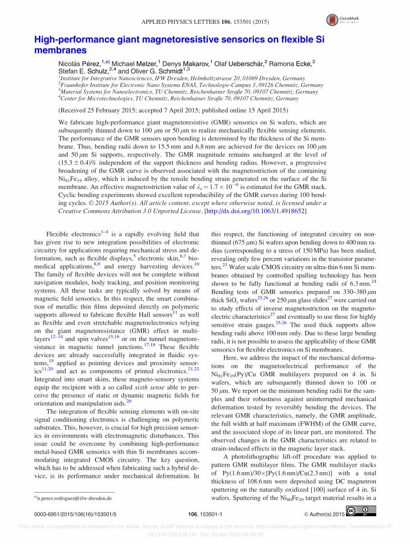
planes into separate rectangular sensor test structures (Figs.
1(a)–1(c)). The lateral dimensions of the diced Si supports
were 5 mm � 18 mm and the 1 mm � 16 mm sensor stripes
had four contact pads to allow reliable resistance measure-
ments under applied field (Fig. 1(e), inset). The GMR sen-
sors were contacted in a four-point configuration using silver
paste and Cu wire of 200 lm in diameter (Fig. 1(e), inset).
The GMR curves of the samples on 100 lm and 50 lm thick
Si membranes are rather similar to the reference samples on
525 lm non-thinned wafers (Fig. 1(e)). The GMR ratio is
defined as DR/R¼ (R�Rsat)/Rsat, where R is the electrical re-
sistance of the sample in an applied magnetic field and Rsat is
the value of the electrical resistance when the GMR stack is
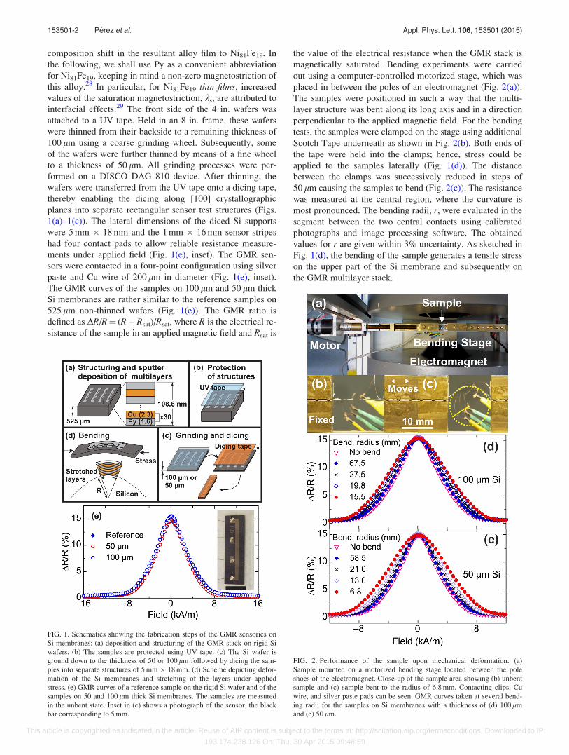
magnetically saturated. Bending experiments were carried
out using a computer-controlled motorized stage, which was
placed in between the poles of an electromagnet (Fig. 2(a)).
The samples were positioned in such a way that the multi-
layer structure was bent along its long axis and in a direction
perpendicular to the applied magnetic field. For the bending
tests, the samples were clamped on the stage using additional
Scotch Tape underneath as shown in Fig. 2(b). Both ends of
the tape were held into the clamps; hence, stress could be
applied to the samples laterally (Fig. 1(d)). The distance
between the clamps was successively reduced in steps of
50 lm causing the samples to bend (Fig. 2(c)). The resistance
was measured at the central region, where the curvature is
most pronounced. The bending radii, r, were evaluated in the
segment between the two central contacts using calibrated
photographs and image processing software. The obtained
values for r are given within 3% uncertainty. As sketched in
Fig. 1(d), the bending of the sample generates a tensile stress
on the upper part of the Si membrane and subsequently on
the GMR multilayer stack.
FIG. 1. Schematics showing the fabrication steps of the GMR sensorics on
Si membranes: (a) deposition and structuring of the GMR stack on rigid Si
wafers. (b) The samples are protected using UV tape. (c) The Si wafer is
ground down to the thickness of 50 or 100 lm followed by dicing the sam-
ples into separate structures of 5 mm � 18 mm. (d) Scheme depicting defor-
mation of the Si membranes and stretching of the layers under applied
stress. (e) GMR curves of a reference sample on the rigid Si wafer and of the
samples on 50 and 100 lm thick Si membranes. The samples are measured
in the unbent state. Inset in (e) shows a photograph of the sensor, the black
bar corresponding to 5 mm.
FIG. 2. Performance of the sample upon mechanical deformation: (a)
Sample mounted on a motorized bending stage located between the pole
shoes of the electromagnet. Close-up of the sample area showing (b) unbent
sample and (c) sample bent to the radius of 6.8 mm. Contacting clips, Cu
wire, and silver paste pads can be seen. GMR curves taken at several bend-
ing radii for the samples on Si membranes with a thickness of (d) 100 lm
and (e) 50 lm.
153501-2 P�erez et al. Appl. Phys. Lett. 106, 153501 (2015)
This article is copyrighted as indicated in the article. Reuse of AIP content is subject to the terms at: http://scitation.aip.org/termsconditions. Downloaded to IP:
193.174.238.126 On: Thu, 30 Apr 2015 09:48:59
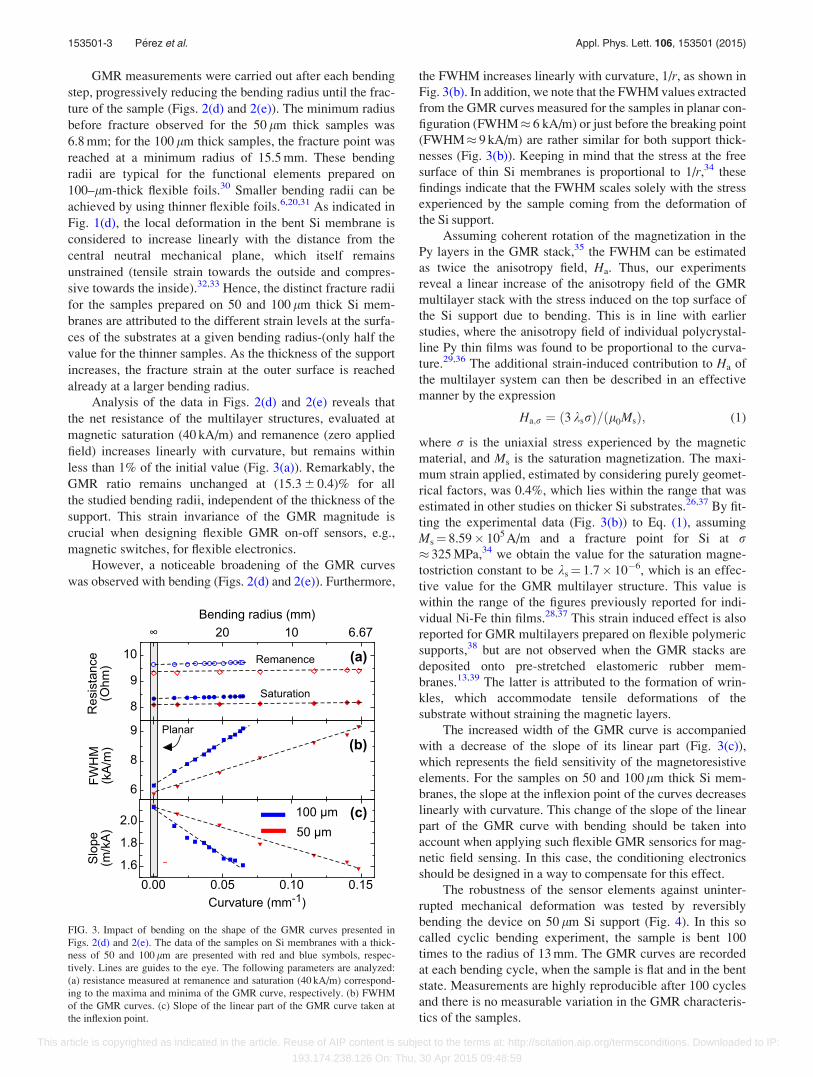
GMR measurements were carried out after each bending
step, progressively reducing the bending radius until the frac-
ture of the sample (Figs. 2(d) and 2(e)). The minimum radius
before fracture observed for the 50 lm thick samples was
6.8 mm; for the 100 lm thick samples, the fracture point was
reached at a minimum radius of 15.5 mm. These bending
radii are typical for the functional elements prepared on
100–lm-thick flexible foils.30 Smaller bending radii can be
achieved by using thinner flexible foils.6,20,31 As indicated in
Fig. 1(d), the local deformation in the bent Si membrane is
considered to increase linearly with the distance from the
central neutral mechanical plane, which itself remains
unstrained (tensile strain towards the outside and compres-
sive towards the inside).32,33 Hence, the distinct fracture radii
for the samples prepared on 50 and 100 lm thick Si mem-
branes are attributed to the different strain levels at the surfa-
ces of the substrates at a given bending radius-(only half the
value for the thinner samples. As the thickness of the support
increases, the fracture strain at the outer surface is reached
already at a larger bending radius.
Analysis of the data in Figs. 2(d) and 2(e) reveals that
the net resistance of the multilayer structures, evaluated at
magnetic saturation (40 kA/m) and remanence (zero applied
field) increases linearly with curvature, but remains within
less than 1% of the initial value (Fig. 3(a)). Remarkably, the
GMR ratio remains unchanged at (15.3 6 0.4)% for all
the studied bending radii, independent of the thickness of the
support. This strain invariance of the GMR magnitude is
crucial when designing flexible GMR on-off sensors, e.g.,
magnetic switches, for flexible electronics.
However, a noticeable broadening of the GMR curves
was observed with bending (Figs. 2(d) and 2(e)). Furthermore,
the FWHM increases linearly with curvature, 1/r, as shown in
Fig. 3(b). In addition, we note that the FWHM values extracted
from the GMR curves measured for the samples in planar con-
figuration (FWHM� 6 kA/m) or just before the breaking point
(FWHM� 9 kA/m) are rather similar for both support thick-
nesses (Fig. 3(b)). Keeping in mind that the stress at the free
surface of thin Si membranes is proportional to 1/r,34 these
findings indicate that the FWHM scales solely with the stress
experienced by the sample coming from the deformation of
the Si support.
Assuming coherent rotation of the magnetization in the
Py layers in the GMR stack,35 the FWHM can be estimated
as twice the anisotropy field, Ha. Thus, our experiments
reveal a linear increase of the anisotropy field of the GMR
multilayer stack with the stress induced on the top surface of
the Si support due to bending. This is in line with earlier
studies, where the anisotropy field of individual polycrystal-
line Py thin films was found to be proportional to the curva-
ture.29,36 The additional strain-induced contribution to Ha of
the multilayer system can then be described in an effective
manner by the expression
Ha;r ¼ ð3 ksrÞ=ðl0MsÞ; (1)
where r is the uniaxial stress experienced by the magnetic
material, and Ms is the saturation magnetization. The maxi-
mum strain applied, estimated by considering purely geomet-
rical factors, was 0.4%, which lies within the range that was
estimated in other studies on thicker Si substrates.26,37 By fit-
ting the experimental data (Fig. 3(b)) to Eq. (1), assuming
Ms¼ 8.59� 105 A/m and a fracture point for Si at r� 325 MPa,34 we obtain the value for the saturation magne-
tostriction constant to be ks¼ 1.7� 10�6, which is an effec-
tive value for the GMR multilayer structure. This value is
within the range of the figures previously reported for indi-
vidual Ni-Fe thin films.28,37 This strain induced effect is also
reported for GMR multilayers prepared on flexible polymeric
supports,38 but are not observed when the GMR stacks are
deposited onto pre-stretched elastomeric rubber mem-
branes.13,39 The latter is attributed to the formation of wrin-
kles, which accommodate tensile deformations of the
substrate without straining the magnetic layers.
The increased width of the GMR curve is accompanied
with a decrease of the slope of its linear part (Fig. 3(c)),
which represents the field sensitivity of the magnetoresistive
elements. For the samples on 50 and 100 lm thick Si mem-
branes, the slope at the inflexion point of the curves decreases
linearly with curvature. This change of the slope of the linear
part of the GMR curve with bending should be taken into
account when applying such flexible GMR sensorics for mag-
netic field sensing. In this case, the conditioning electronics
should be designed in a way to compensate for this effect.
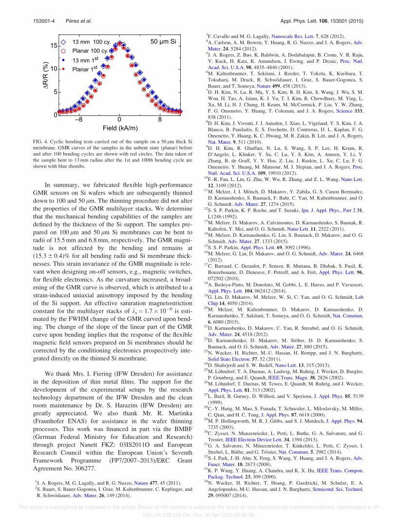
The robustness of the sensor elements against uninter-
rupted mechanical deformation was tested by reversibly
bending the device on 50 lm Si support (Fig. 4). In this so
called cyclic bending experiment, the sample is bent 100
times to the radius of 13 mm. The GMR curves are recorded
at each bending cycle, when the sample is flat and in the bent
state. Measurements are highly reproducible after 100 cycles
and there is no measurable variation in the GMR characteris-
tics of the samples.
FIG. 3. Impact of bending on the shape of the GMR curves presented in
Figs. 2(d) and 2(e). The data of the samples on Si membranes with a thick-
ness of 50 and 100 lm are presented with red and blue symbols, respec-
tively. Lines are guides to the eye. The following parameters are analyzed:
(a) resistance measured at remanence and saturation (40 kA/m) correspond-
ing to the maxima and minima of the GMR curve, respectively. (b) FWHM
of the GMR curves. (c) Slope of the linear part of the GMR curve taken at
the inflexion point.
153501-3 P�erez et al. Appl. Phys. Lett. 106, 153501 (2015)
This article is copyrighted as indicated in the article. Reuse of AIP content is subject to the terms at: http://scitation.aip.org/termsconditions. Downloaded to IP:
193.174.238.126 On: Thu, 30 Apr 2015 09:48:59
In summary, we fabricated flexible high-performance
GMR sensors on Si wafers which are subsequently thinned
down to 100 and 50 lm. The thinning procedure did not alter
the properties of the GMR multilayer stacks. We determine
that the mechanical bending capabilities of the samples are
defined by the thickness of the Si support. The samples pre-
pared on 100 lm and 50 lm Si membranes can be bent to
radii of 15.5 mm and 6.8 mm, respectively. The GMR magni-
tude is not affected by the bending and remains at
(15.3 6 0.4)% for all bending radii and Si membrane thick-
nesses. This strain invariance of the GMR magnitude is rele-
vant when designing on-off sensors, e.g., magnetic switches,
for flexible electronics. As the curvature increased, a broad-
ening of the GMR curve is observed, which is attributed to a
strain-induced uniaxial anisotropy imposed by the bending
of the Si support. An effective saturation magnetostriction
constant for the multilayer stacks of ks¼ 1.7� 10�6 is esti-
mated by the FWHM change of the GMR curved upon bend-
ing. The change of the slope of the linear part of the GMR
curve upon bending implies that the response of the flexible
magnetic field sensors prepared on Si membranes should be
corrected by the conditioning electronics prospectively inte-
grated directly on the thinned Si membrane.
We thank Mrs. I. Fiering (IFW Dresden) for assistance
in the deposition of thin metal films. The support for the
development of the experimental setups by the research
technology department of the IFW Dresden and the clean
room maintenance by Dr. S. Harazim (IFW Dresden) are
greatly appreciated. We also thank Mr. R. Martinka
(Fraunhofer ENAS) for assistance in the wafer thinning
processes. This work was financed in part via the BMBF
(German Federal Ministry for Education and Research)
through project Nanett FKZ: 03IS2011O and European
Research Council within the European Union’s Seventh
Framework Programme (FP7/2007–2013)/ERC Grant
Agreement No. 306277.
1J. A. Rogers, M. G. Lagally, and R. G. Nuzzo, Nature 477, 45 (2011).2S. Bauer, S. Bauer-Gogonea, I. Graz, M. Kaltenbrunner, C. Keplinger, and
R. Schw€odiauer, Adv. Mater. 26, 149 (2014).
3F. Cavallo and M. G. Lagally, Nanoscale Res. Lett. 7, 628 (2012).4A. Carlson, A. M. Bowen, Y. Huang, R. G. Nuzzo, and J. A. Rogers, Adv.
Mater. 24, 5284 (2012).5J. A. Rogers, Z. Bao, K. Baldwin, A. Dodabalapur, B. Crone, V. R. Raju,
V. Kuck, H. Katz, K. Amundson, J. Ewing, and P. Drzaic, Proc. Natl.
Acad. Sci. U.S.A. 98, 4835–4840 (2001).6M. Kaltenbrunner, T. Sekitani, J. Reeder, T. Yokota, K. Kuribara, T.
Tokuhara, M. Drack, R. Schw€odiauer, I. Graz, S. Bauer-Gogonea, S.
Bauer, and T. Someya, Nature 499, 458 (2013).7D. H. Kim, N. Lu, R. Ma, Y. S. Kim, R. H. Kim, S. Wang, J. Wu, S. M.
Won, H. Tao, A. Islam, K. J. Yu, T. I. Kim, R. Chowdhury, M. Ying, L.
Xu, M. Li, H. J. Chung, H. Keum, M. McCormick, P. Liu, Y. W. Zhang,
F. G. Omenetto, Y. Huang, T. Coleman, and J. A. Rogers, Science 333,
838 (2011).8D. H. Kim, J. Viventi, J. J. Amsden, J. Xiao, L. Vigeland, Y. S. Kim, J. A.
Blanco, B. Panilaitis, E. S. Frechette, D. Contreras, D. L. Kaplan, F. G.
Omenetto, Y. Huang, K. C. Hwang, M. R. Zakin, B. Litt, and J. A. Rogers,
Nat. Mater. 9, 511 (2010).9D. H. Kim, R. Ghaffari, N. Lu, S. Wang, S. P. Lee, H. Keum, R.
D’Angelo, L. Klinker, Y. Su, C. Lu, Y. S. Kim, A. Ameen, Y. Li, Y.
Zhang, B. de Graff, Y. Y. Hsu, Z. Liu, J. Ruskin, L. Xu, C. Lu, F. G.
Omenetto, Y. Huang, M. Mansour, M. J. Slepian, and J. A. Rogers, Proc.
Natl. Acad. Sci. U.S.A. 109, 19910 (2012).10F.-R. Fan, L. Lin, G. Zhu, W. Wu, R. Zhang, and Z. L. Wang, Nano Lett.
12, 3109 (2012).11M. Melzer, J. I. M€onch, D. Makarov, Y. Zabila, G. S. Canon Bermudez,
D. Karnaushenko, S. Baunack, F. Bahr, C. Yan, M. Kaltenbrunner, and O.
G. Schmidt, Adv. Mater. 27, 1274 (2015).12S. S. P. Parkin, K. P. Roche, and T. Suzuki, Jpn. J. Appl. Phys., Part 2 31,
L1246 (1992).13M. Melzer, D. Makarov, A. Calvimontes, D. Karnaushenko, S. Baunak, R.
Kaltofen, Y. Mei, and O. G. Schmidt, Nano Lett. 11, 2522 (2011).14M. Melzer, D. Karnaushenko, G. Lin, S. Baunack, D. Makarov, and O. G.
Schmidt, Adv. Mater. 27, 1333 (2015).15S. S. P. Parkin, Appl. Phys. Lett. 69, 3092 (1996).16M. Melzer, G. Lin, D. Makarov, and O. G. Schmidt, Adv. Mater. 24, 6468
(2012).17C. Barraud, C. Deranlot, P. Seneor, R. Mattana, B. Dlubak, S. Fusil, K.
Bouzehouane, D. Deneuve, F. Petroff, and A. Fert, Appl. Phys. Lett. 96,
072502 (2010).18A. Bedoya-Pinto, M. Donolato, M. Gobbi, L. E. Hueso, and P. Vavassori,
Appl. Phys. Lett. 104, 062412 (2014).19G. Lin, D. Makarov, M. Melzer, W. Si, C. Yan, and O. G. Schmidt, Lab
Chip 14, 4050 (2014).20M. Melzer, M. Kaltenbrunner, D. Makarov, D. Karnaushenko, D.
Karnaushenko, T. Sekitani, T. Someya, and O. G. Schmidt, Nat. Commun.
6, 6080 (2015).21D. Karnaushenko, D. Makarov, C. Yan, R. Streubel, and O. G. Schmidt,
Adv. Mater. 24, 4518 (2012).22D. Karnaushenko, D. Makarov, M. St€ober, D. D. Karnaushenko, S.
Baunack, and O. G. Schmidt, Adv. Mater. 27, 880 (2015).23N. Wacker, H. Richter, M.-U. Hassan, H. Rempp, and J. N. Burghartz,
Solid State Electron. 57, 52 (2011).24D. Shahrjerdi and S. W. Bedell, Nano Lett. 13, 315 (2013).25M. L€ohndorf, T. A. Duenas, A. Ludwig, M. Ruhrig, J. Wecker, D. Burgler,
P. Grunberg, and E. Quandt, IEEE Trans. Magn. 38, 2826 (2002).26M. L€ohndorf, T. Duenas, M. Tewes, E. Quandt, M. Ruhrig, and J. Wecker,
Appl. Phys. Lett. 81, 313 (2002).27L. Baril, B. Gurney, D. Wilhoit, and V. Speriosu, J. Appl. Phys. 85, 5139
(1999).28C.-Y. Hung, M. Mao, S. Funada, T. Schneider, L. Miloslavsky, M. Miller,
C. Qian, and H. C. Tong, J. Appl. Phys. 87, 6618 (2000).29M. P. Hollingworth, M. R. J. Gibbs, and S. J. Murdoch, J. Appl. Phys. 94,
7235 (2003).30C. Zysset, N. Munzenrieder, L. Petti, L. Buthe, G. A. Salvatore, and G.
Troster, IEEE Electron Device Lett. 34, 1394 (2013).31G. A. Salvatore, N. M€unzenrieder, T. Kinkeldei, L. Petti, C. Zysset, I.
Strebel, L. B€uthe, and G. Tr€oster, Nat. Commun. 5, 2982 (2014).32S.-I. Park, J.-H. Ahn, X. Feng, S. Wang, Y. Huang, and J. A. Rogers, Adv.
Funct. Mater. 18, 2673 (2008).33K. P. Wang, Y. Huang, A. Chandra, and K. X. Hu, IEEE Trans. Compon.
Packag. Technol. 23, 309 (2000).34N. Wacker, H. Richter, T. Hoang, P. Gazdzicki, M. Schulze, E. A.
Angelopoulos, M-U. Hassan, and J. N. Burghartz, Semicond. Sci. Technol.
29, 095007 (2014).
FIG. 4. Cyclic bending tests carried out of the sample on a 50 lm thick Si
membrane. GMR curves of the samples in the unbent state (planar) before
and after 100 bending cycles are shown with red circles. The data taken of
the sample bent to 13 mm radius after the 1st and 100th bending cycle are
shown with blue rhombs.
153501-4 P�erez et al. Appl. Phys. Lett. 106, 153501 (2015)
This article is copyrighted as indicated in the article. Reuse of AIP content is subject to the terms at: http://scitation.aip.org/termsconditions. Downloaded to IP:
193.174.238.126 On: Thu, 30 Apr 2015 09:48:59
35R. Coehoorn, “Giant magnetoresistance and magnetic interactions in
exchange-biased spin valves,” in Handbook of Magnetic Materials, edited
by K. H. J. Buschow (Elsevier, Amsterdam 2003), Vol. 15.36C. S. Gudeman, IEEE Trans. Magn. 26, 2580 (1990).37T. J. Gafron, S. E. Russek, and S. L. Burkett, J. Vac. Sci. Technol. A 19,
1195 (2001).
38Y.-F. Chen, Y. Mei, R. Kaltofen, J. I. M€onch, J. Schumann, J.
Freudenberger, H.-J. Klauss, and O. G. Schmidt, Adv. Mater. 20, 3224
(2008).39M. Melzer, D. Karnaushenko, D. Makarov, L. Baraban, A. Calvimontes, I.
M€onch, R. Kaltofen, Y. Mei, and O. G. Schmidt, RSC Adv. 2, 2284
(2012).
153501-5 P�erez et al. Appl. Phys. Lett. 106, 153501 (2015)
This article is copyrighted as indicated in the article. Reuse of AIP content is subject to the terms at: http://scitation.aip.org/termsconditions. Downloaded to IP:
193.174.238.126 On: Thu, 30 Apr 2015 09:48:59