
Modulation Methods and Applications - MDPI
30
energies Review Review of Isolated Matrix Inverters: Topologies, Modulation Methods and Applications Oleksandr Korkh, Andrei Blinov * , Dmitri Vinnikov and Andrii Chub Department of Electrical Power Engineering and Mechatronics, Tallinn University of Technology, 19086 Tallinn, Estonia; [email protected] (O.K.); [email protected] (D.V.); [email protected] (A.C.) * Correspondence: [email protected] Received: 20 April 2020; Accepted: 7 May 2020; Published: 11 May 2020 Abstract: This paper presents a review of isolated matrix inverters. The study contributes to creating a point of reference for a comprehensive classification of existing solutions. Over 30 topologies were reviewed, and the main advantages and disadvantages discussed. Applications of isolated matrix inverters are summarized in a tabular form to demonstrate their flexibility for different power and voltage levels achieved due to the presence of a transformer. These inverters have been proposed for the uninterruptible power supplies, high and low-voltage/power photovoltaic systems, low-power fuel cell, different low- and high-voltage battery and/or electric vehicle chargers, audio amplifiers. The fully controlled switches on both terminals of these converters typically can provide the bidirectional power transfer capability, which is also addressed for most of the topologies, but requires some modification in their modulation strategy. Average efficiency of today’s isolated matrix inverters is comparable with the two-stage power converters; however, they can provide higher reliability and lower cost. Keywords: isolated matrix inverter; current source inverter; voltage source inverter; bridge; push–pull; modulation methods; soft switching 1. Introduction Climate change caused by human activities resulting in excessive pollution by greenhouse gases is considered the main threat to the sustainable development of humanity [1]. The first attempt to limit the pollution was reflected in the Kyoto Protocol of 1992 [2]. Later, it was recognized that this initiative is not sufficient to adequately address climate change [3]. Eventually, the Paris Agreement of 2016 was introduced to strengthen national efforts towards climate change mitigation [4]. The energy intensity is considered the key metric for national economies and reflects energy use in equivalent kilograms of oil needed to produce a unity of the national global domestic product [5]. This can be improved via decarbonization of energy generation facilities and improvement of energy efficiency of industry, building stock, agriculture, etc. Renewable energy generation is considered the main solution for decarbonization of the energy generation industry [6,7]. Even though hydroelectric and biomass technologies dominate this sector, non-conventional renewables are projected to increase their share to over 60% with the dominance of electrical energy generation [8]. This will be supported by accelerated rates of electrification of the industry and the private sector. It is expected that even heating will be widely electrified in the next 30 years [9]. Evidently, electrification will require new approaches to energy processing and transportation. Power electronics is becoming a critical technology that can enable the paradigm shift to decentralized renewable energy generation and massive electrification [10]. Emerging applications of power electronics are countless: renewable energy generation from multi-MW to sub-kW scale, electric Energies 2020, 13, 2394; doi:10.3390/en13092394 www.mdpi.com/journal/energies
Transcript of Modulation Methods and Applications - MDPI
energies
Review
Review of Isolated Matrix Inverters: Topologies,Modulation Methods and Applications
Oleksandr Korkh, Andrei Blinov * , Dmitri Vinnikov and Andrii Chub
Department of Electrical Power Engineering and Mechatronics, Tallinn University of Technology,19086 Tallinn, Estonia; [email protected] (O.K.); [email protected] (D.V.);[email protected] (A.C.)* Correspondence: [email protected]
Received: 20 April 2020; Accepted: 7 May 2020; Published: 11 May 2020�����������������
Abstract: This paper presents a review of isolated matrix inverters. The study contributes to creatinga point of reference for a comprehensive classification of existing solutions. Over 30 topologieswere reviewed, and the main advantages and disadvantages discussed. Applications of isolatedmatrix inverters are summarized in a tabular form to demonstrate their flexibility for differentpower and voltage levels achieved due to the presence of a transformer. These inverters have beenproposed for the uninterruptible power supplies, high and low-voltage/power photovoltaic systems,low-power fuel cell, different low- and high-voltage battery and/or electric vehicle chargers, audioamplifiers. The fully controlled switches on both terminals of these converters typically can providethe bidirectional power transfer capability, which is also addressed for most of the topologies, butrequires some modification in their modulation strategy. Average efficiency of today’s isolated matrixinverters is comparable with the two-stage power converters; however, they can provide higherreliability and lower cost.
Keywords: isolated matrix inverter; current source inverter; voltage source inverter; bridge; push–pull;modulation methods; soft switching
1. Introduction
Climate change caused by human activities resulting in excessive pollution by greenhouse gasesis considered the main threat to the sustainable development of humanity [1]. The first attempt to limitthe pollution was reflected in the Kyoto Protocol of 1992 [2]. Later, it was recognized that this initiativeis not sufficient to adequately address climate change [3]. Eventually, the Paris Agreement of 2016 wasintroduced to strengthen national efforts towards climate change mitigation [4]. The energy intensityis considered the key metric for national economies and reflects energy use in equivalent kilogramsof oil needed to produce a unity of the national global domestic product [5]. This can be improvedvia decarbonization of energy generation facilities and improvement of energy efficiency of industry,building stock, agriculture, etc.
Renewable energy generation is considered the main solution for decarbonization of the energygeneration industry [6,7]. Even though hydroelectric and biomass technologies dominate this sector,non-conventional renewables are projected to increase their share to over 60% with the dominanceof electrical energy generation [8]. This will be supported by accelerated rates of electrification ofthe industry and the private sector. It is expected that even heating will be widely electrified in thenext 30 years [9]. Evidently, electrification will require new approaches to energy processing andtransportation. Power electronics is becoming a critical technology that can enable the paradigm shift todecentralized renewable energy generation and massive electrification [10]. Emerging applications ofpower electronics are countless: renewable energy generation from multi-MW to sub-kW scale, electric
Energies 2020, 13, 2394; doi:10.3390/en13092394 www.mdpi.com/journal/energies

Energies 2020, 13, 2394 2 of 30
and hybrid electric vehicles and their on- and off-board charging, high-voltage DC energy transmission,battery energy storage systems (BESS) from utility level to the behind-the-meter applications, energyharvesting for Internet of Things devices, wearables, microgrids (AC, DC and hybrid) and theirinterconnection, energy-efficient buildings with on-site energy generation, etc.
The increased use of alternative and renewable energy sources, like wind and solar, together withthe development of energy storage technologies, such as Li-ion batteries, supercapacitors and fuel cells,fosters the need for various power electronic converters in the present electric energy systems [11–15].Electronic power technology for large-scale renewable energy generation is approaching maturity andsees evolutional improvements in topologies, used semiconductor and passive components. At thesame time, disruptive innovation is expected in their control by the integration of smart functionalitiessecured with blockchain (distributed ledger) technology [16,17]. Meanwhile, the dispersion of energygeneration is associated with the new incentives for decarbonization of building stock. It has beenshown that nearly zero energy buildings can be economically viable when energy-saving constructiontechnologies are complemented with on-site generation of heat and electricity [18]. This has resulted inthe rapid growth of residential renewable energy generation technologies, such as rooftop and buildingintegrated photovoltaic (PV) systems, low-voltage residential BESSs, small wind turbines, fuel cells(FCs), etc. [19,20]. All of these feature different voltage and power levels and thus require numerouspower electronic converter types. Moreover, additional converters are required to interface systemshaving various voltage levels with common DC or AC bus [21,22]. Increased electrification will requireenergy storage not only to balance the utility grid to withstand intermittent variations in renewableenergy generation, but also to provide an uninterruptible power supply to critical loads [23,24]. Othergrowing markets that benefit from advancements in power electronic technologies are hybrid andelectric vehicles [25], electrified railway [26], variable speed drives across industry [27] and flexiblepower systems [28]. Increased demand for the development of technologies based on power electronicconverters put additional pressure on the industry to provide new solutions with minimal cost andhigh reliability to facilitate faster decarbonization.
In the BESS, PV and FC applications, a power electronic converter has to operate with a variableDC source that should be interfaced with the AC grid. In such systems, the main challenges aremostly associated with providing voltage step-up from a low-voltage energy source, like a battery or toprovide galvanic isolation as a safety measure, such as required in EV charging. Typically, to achievedemanded functionality, a two-stage power electronic system is used (Figure 1a) [29–33]. Variableinput DC voltage is first stabilized at a DC-link capacitor by a DC–DC converter that often features ahigh-frequency (HF) transformer (HFT) for both voltages matching and the galvanic isolation. It isthen followed by an inverter stage that converts the stabilized DC voltage of the appropriate levelinto the AC voltage. These systems offer a good regulation range and are widely used in practicalapplications [29–34].
An alternative approach is to apply isolated DC–AC topologies without an evident intermediateDC-link. In these converters, the HFT secondary voltage can be converted to low frequency (LF) ACusing an active rectifier and unfolder (Figure 1b) [35–42], or by using single HF AC to LF AC conversion(Figure 1c) [43–53]. Despite both of these approaches are commonly referred to as single-stage DC–ACconverters, the systems with unfolding stage technically feature an additional low-frequency link (withrectified sine-wave) and, therefore, are considered as a quasi-single stage in this paper. On the otherhand, the topologies with unified HF AC to LF AC stage are performing AC–AC conversion directly,using bidirectional semiconductor switches, which is a distinctive feature of matrix converters [54].In the literature, such systems are also referred to as HF-link inverters [39,52], cycloconverters [43,48]or single-stage inverters (converters) [30,32], but are all considered as isolated matrix inverters in thisreview. These systems are often capable of transferring power in both directions and can achieve softswitching conditions in semiconductors with advanced modulation methods [46–56]. Such features,together with a wide range of possible industrial applications, have attracted increased interest ofresearch groups in isolated matrix inverters for many years.

Energies 2020, 13, 2394 3 of 30
Modern single-stage converters with fully controlled semiconductor devices started to appear inthe literature in the late 1980s [57], mostly targeting uninterruptible power supplies [58,59]. Later, theirapplication area was extended to PV microinverters [60,61], FC [42,62,63], Li-ion battery storage [64],railroad [65], electric vehicle charging [66], motor drive [67] and residential applications [22,62].Currently, the two-stage galvanically isolated inverters are an industry-accepted technology establishedin numerous applications, while the quasi-single-stage has also been used in emerging applicationssuch as PV microinverters [68,69], recently adopted in residential BESSs [70–73]. The isolated matrixinverters are an emerging technology that has not yet reached maturity and good industrial awareness;however, this technology shows good potential for industrial adoption, as was demonstrated in [53,74].
Figure 1. General structure of isolated matrix inverters: (a) two-stage, (b) quasi single-stage,(c) single-stage. LF AC—grid frequency; HF AC—switching frequency.
Despite a multitude of isolated matrix inverter concepts presented for various applications,no classifications or reviews summarizing the features and potential of this technology have beenreported. The aim of this paper is to give an overview of existing single-stage matrix inverters, classifytheir topologies, modulation methods and applications in order to get the reader a better understandingof the potential and limitations of such systems. The paper is arranged as follows: in Section 2,the classification based on topology types and modulation methods is proposed. Section 3 addressesthe current source inverter (CSI) based topologies, followed by the description of the voltage sourceinverter (VSI) based topologies in Section 4. Section 5 discusses the main features and applications ofthe highlighted topologies. Finally, the conclusions and further research directions are presented.
2. Systematization and Classification
Various isolated matrix inverter topologies have been reported for different applications, rangingfrom low-voltage and low-power [60,61,75] to high-voltage high-power [76], which proves the versatilityof this technology and justifies the need for systematization of existing knowledge to establish pointsof reference. As mentioned in the previous section, a common property of such converters lies inthe absence of an evident DC-link and presence of the direct AC-to-AC conversion stage. Generally,the DC-side of an isolated matrix inverter features a half-bridge (HB), full-bridge (FB) or push–pull(PP) stage that is connected to the primary winding of HFT. The AC-side connects the HFT secondary

Energies 2020, 13, 2394 4 of 30
to the grid using HF AC to LF AC stage. The AC-side can be a current-source inverter (CSI) type [46]or a voltage-source inverter (VSI) type [77]. In the CSI-type, the current IO is constantly flowing inone of the legs and either LC or LCL filter is used (Figure 2a), whereas the VSI-type has the diagonalsswitched with certain dead time and generally utilizes a CL filter, and in this case, the current IO is notcontinuous (Figure 2b).
Figure 2. Generalized representation over one switching period of currents and voltages for differentisolated matrix inverter types and availability of resonant tank: (a) current source inverter (CSI),(b) voltage-source inverter (VSI), (c) resonant, (d) non-resonant.
The converters that are based on the two-winding transformer are typically HB- or FB-type [57,60,61].On the other hand, central-tapped or multi-winding transformers enable the use of other configurations,like PP [78] or three-leg [79]. The PP topologies generally employ the central tap transformer, and thesemiconductors have double voltage stress, but, at the same time, they allow for the reduction of thenumber of semiconductor devices.
Most modern isolated matrix inverters feature soft switching in semiconductors that is achievedusing special modulation strategies [46–56], resonant circuits [60,66,80] or active auxiliary circuits [81–85].In addition, these methods aim to reduce semiconductor voltage stresses [85]. For the resonanttopologies, the transformer current ITr2 is usually close to the sinusoidal (Figure 2c), whereas in the caseof non-resonant topologies, the shape of current ITr2 is typically close to square-wave or trapezoidal(Figure 2d).
The sine wave modulation can be applied either for DC or AC sides of the converter. In the caseof the DC-side modulation (primary side modulation), the shape of the output voltage (current) isformed using pulse width modulation (PWM) [47] or phase shift modulation (PSM) [48] applied to theDC-side switches. The AC side, in this case, is usually working as a rectifier. Another common strategyis the secondary side modulation. In this case, the DC switches are working as an inverter, formingthe square wave voltage pulses at the HFT primary. After this, the AC-side switches are forming therequired shape of the voltage (current) based on PSM [46] or PWM [47]. For the resonant topologies,the frequency modulation (FM) [66] is usually applied, which allows changing the gain under differentpower ratings.
Two main strategies of the PWM are used—unipolar and bipolar. Unipolar PWM (UPWM) [47,49,75]is widely employed and allows achieving zero voltage switching (ZVS) for the AC-side switches.The utilization of the bipolar PWM (BPWM) [81] has been reported to have lower total harmonicdistortion than the UPWM. The PSM modulation is usually based on only one shift carrier for theCSI [46,48], while in the VSI based topologies, PSM with more than one phase shift is typically usedto achieve better quality of the output voltage [86]. More sophisticated methods additionally use FMto increase the ZVS range [66]; moreover, the amplitude modulation (AM) [80] was also addressed.These are the low-level modulation techniques that are employed in converter modulators to generatethe switching sequence within a single switching period and ensure that an inverter can performthe input voltage regulation and the output current control (Figure 3). Hence, this paper considersmodulation strategy as the main control feature in each reviewed topology. To achieve the LF sinusoidalvoltage/current at the output, a higher-level control/modulation (controller in Figure 3a) method has tobe applied to define the control variables applied to the low-level modulators (Vmod) across the gridfrequency period, i.e. PWM duty cycle, PSM phase shift or both. Typical higher-level control/modulationmethods are the sinusoidal modulation [58] in the one-phase system, the space vector modulation [87]

Energies 2020, 13, 2394 5 of 30
in the three-phase, or model predictive control [88]. They define the input parameters applied to thelow-level modulator(s) typically based on PWM or PSM, as discussed above.
Figure 3. Generalized representation of (a)control and (b) modulation for the isolated matrix inverters.
The isolated matrix inverters could be realized with the metal oxide semiconductor field-effecttransistor (MOSFET) [89], the insulated-gate bipolar transistor (IGBT) [90], gate turn-off thyristor(GTO) [91] or the reverse blocking IGBT (RB IGBT) [92–95] semiconductors, depending on the powerand voltage level and application. The DC side is generally formed by unidirectional devices (Figure 4a),while the AC side usually features bidirectional switches (Figure 4b). The bidirectional switches for theAC side are typically realized by two identical devices in common source (emitter, cathode) configurationor the antiparallel reverse blocking switches can be applied. In some cases, the bidirectional switcheswith the middle connection point can also be used (Figure 4c) (see also [96–107]).
Figure 4. The types of the semiconductors (a) unidirectional switch, (b) bidirectional switch,(c) bidirectional switch with the middle connection point.
Energies 2020, 13, 2394 6 of 30
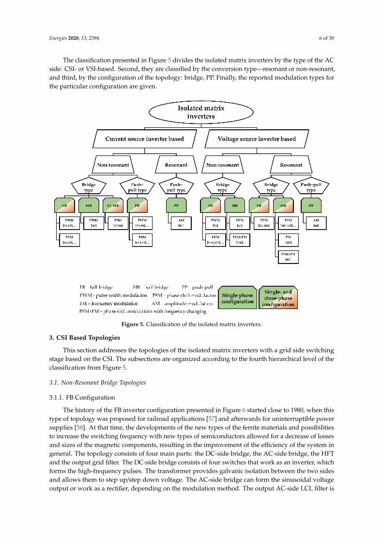
The classification presented in Figure 5 divides the isolated matrix inverters by the type of the ACside: CSI- or VSI-based. Second, they are classified by the conversion type—resonant or non-resonant,and third, by the configuration of the topology: bridge, PP. Finally, the reported modulation types forthe particular configuration are given.
Figure 5. Classification of the isolated matrix inverters.
3. CSI Based Topologies
This section addresses the topologies of the isolated matrix inverters with a grid side switchingstage based on the CSI. The subsections are organized according to the fourth hierarchical level of theclassification from Figure 5.
3.1. Non-Resonant Bridge Topologies
3.1.1. FB Configuration
The history of the FB inverter configuration presented in Figure 6 started close to 1980, when thistype of topology was proposed for railroad applications [57] and afterwards for uninterruptible powersupplies [58]. At that time, the developments of the new types of the ferrite materials and possibilitiesto increase the switching frequency with new types of semiconductors allowed for a decrease of lossesand sizes of the magnetic components, resulting in the improvement of the efficiency of the system ingeneral. The topology consists of four main parts: the DC-side bridge, the AC-side bridge, the HFTand the output grid filter. The DC-side bridge consists of four switches that work as an inverter, whichforms the high-frequency pulses. The transformer provides galvanic isolation between the two sidesand allows them to step up/step down voltage. The AC-side bridge can form the sinusoidal voltageoutput or work as a rectifier, depending on the modulation method. The output AC-side LCL filter is

Energies 2020, 13, 2394 7 of 30
used to filter the high-frequency pulses. Given the realization of bidirectional switches in the AC sideusing two discrete devices, this leads to a distinct disadvantage–a relatively high number of activesemiconductor devices required.
Figure 6. Full-bridge (FB) configuration (a) and modulation(b) proposed in [52].
Another major challenge for the isolated FB configuration inverter topology is that the transformerleakage inductance and the output filter inductor both serve as current sources for the AC-side bridge.Thus, the AC-side bridge operates as a current breaker, which endures high-voltage spikes due tothe cutoff of the leakage inductor current. The natural commutation principle for this converter wasproposed in [59]. In addition, various other modulation methods using DC- or AC-side switches werepresented for the current topology [46–52]. These methods typically allow utilizing energy stored inthe leakage inductance to create soft switching conditions for semiconductors, which also particularlyor fully solves the mentioned problem of high-voltage overshoots. The topology features the capabilityof bidirectional power flow without any additional auxiliary circuit.
In [46], the 40 kVA bidirectional converter for medium voltage converter (MVC) applicationwas proposed. This work presents a special multi-mode quasi-resonant PSM method, which allowsachieving soft switching in all semiconductor devices. The additional snubber capacitor is addedfor DC-side semiconductors and RCD for the AC side to reduce turn-off losses and ringing. Specialmulti-mode modulation allows the creation of the additional quasi-resonant interval, which is activatednear the zero-crossing point. It is utilizing the resonant circuit formed by the DC-side snubber capacitorand transformer leakage inductance to achieve soft switching at the current zero-crossing point.The details of the modulation method are described in [65]. The experimental waveforms confirmthat the method is verified, and the converter can operate without any additional damping circuit forthe leakage inductance energy. At the same time, the optimization of the transformer and snubbercapacitance can be a point of the discussion, because this can significantly influence of the converterefficiency, especially at the higher step-up ratio of the transformer.
Two UPWM based modulation methods for the FB isolated matrix inverter are reported in [47],both of these methods allow achieving the soft switching for the AC-side switches. In contrast, the DCside has only the ZVS turn-on transient. The first method allows operating four switches at the ACside at line frequency, further reducing the remaining switching loss and improving the efficiency.The authors applied the hybrid structure of the switches at the AC side –four of them are IGBT withgrid frequency switching and four MOSFET with high working frequency. This allows price reductionof the converter, which was the authors’ aim. The second modulation method is proposed for the fullMOSFET bridge configuration. In this method, two of the switches working with the line frequency,two–as synchronous switches, and all the other are forming the output voltage. The authors verifiedthe experimental 1.2-kW prototype with 400-V DC input voltage and 240-V AC RMS output usingone to one isolation transformer. The peak efficiency of the system is 96% for the full silicon carbide(SiC) MOSFET design. In [108], the same group of authors presented applications for this converterin the high-frequency distributed power delivery system. This utilization allows elimination of thetraditional low-frequency transformer and its replacement it with HFT. The potential target applicationis air and ground transportation and renewable energy systems.

Energies 2020, 13, 2394 8 of 30
In some studies, the leakage inductor energy is redirected to the additional auxiliary circuit, whichallows the clamp of the voltage overshoot. In [48], the new modulation method based on the DC-sidePSM is addressed for the FB inverter operation. For the minimization of voltage overshoot acrossAC-side switches, the clamping circuit with the rectifier bridge, capacitor and DC–DC converter isapplied. The energy from the AC side is returned to the DC input and reused again in the converter.The topology is verified with 1 kW with 270 V of input and 100-V RMS at the output as UPS inverter.Other clamping circuit approaches were addressed in [49–51,109]. These papers present different typesof regenerative flyback snubber. Since this snubber is technically a separate converter, in additionto voltage clamping, it can provide additional features for the topology: reduce the amount of thecirculation current through the main switches, improve the soft-start procedure or improve the qualityof the current in the case of non-unity power factor. The energy stored in the snubber capacitor can beutilized in two ways–being reused in the next switching cycle of the conversion, as proposed in [49,50]or transferred back to the DC side and reused again as shown in [109]. In addition, it is claimed to allowimproving the efficiency of the converter in general. In [110], different snubbers for the minimization ofthe influence of high step-up transformer are analyzed for the case of the integration of low-voltage DCsource to the grid. On the other hand, the utilization of the snubbers requires an additional transformeror two flyback transformers, switches, diodes, capacitors and additional control channels and isolateddrivers. The utilization of this snubber can be more suitable for the high-power converter. For thelower-power converters, this solution can be less optimal, considering the price and overall complexity.
Many high-power converters commonly use bridge-type topologies due to the better utilizationof the switches and lower stresses. The FB topologies can be extended to the three-phase grid system,as presented in [53,59,76,111]. In this case, at the AC side, an additional leg is supplied and themodulation method is extended for the three-phase system (Figure 7).
Figure 7. Three-phase FB configuration.
3.1.2. FB Configuration with Three Legs at the DC Side
In [79], the AC side PSM modulated PV microinverter is proposed (Figure 8). The topology utilizesthree switching legs and a special high-frequency transformer. The additional bridge leg operates witha phase shift to the main bridge and allows generation of the two-step voltage waveforms, whichare afterwards converted to the AC voltage. The two-step voltage allows reducing the ringing of theAC-side switches. The topology allows achieving the soft switching in all semiconductors at the ACside, while on the DC side, only two switches have hard transients. This solution is suggested toimprove the efficiency of the system compared to the topology with the RCD snubber at the AC side.The peak efficiency reported is 95%.

Energies 2020, 13, 2394 9 of 30
Figure 8. FB topology with the three switching legs at the DC side (a) and modulation (b) in [79].
3.1.3. FB Configuration with the Reconfigurable AC Side
The topology reported in [42,62] is proposed as a unidirectional inverter for the FC applications(Figure 9). It features two transformers and two bidirectional AC side bridges, which can be connectedin series or in parallel, providing the universal output. The topology utilizes the SPWM at the DC side,while half of the AC-side switches work with the grid frequency to minimize the switching losses in theconverter. The design focuses on the universality of the output voltage and is suitable for both 230 Vand 110 V and has a high step-up factor to achieve the connection 30–60-V fuel cell and is claimedto be optimal in terms of weight and cost. The authors achieved a peak efficiency of 92.5% for theproposed concept. The leakage inductances of the transformer are utilized for the soft switching inthe semiconductors, but at the same time, the voltage overshoot appears across the AC-side switches.This suggests that the design and optimization of the transformer can be further considered to achievebetter efficiency and reduce the stresses in the topology.
Figure 9. FB topology with the reconfigurable AC side (a) and modulation (b) shown in [62].
3.1.4. The FB Configuration with PP at the DC Side
Figure 10 shows the topology reported in [78] as a unidirectional inverter for renewable energysources. The topology has two switches at the DC side connected to a central-tapped transformer,forming the PP configuration. The AC side features the FB configuration. The multiple-carrier PWM is

Energies 2020, 13, 2394 10 of 30
proposed for this topology. It was suggested that this technique allows reducing the complexity of thecontrol algorithm for the inverter. The topology is suitable for low power applications; the simulationresults of the 200-W prototype were shown for 48 VDC input voltage and 127-V RMS output voltage,using a transformer with a turns ratio of 1 to 4.2. An alternative configuration of a bidirectionalconverter based on the Cuk, SEPIC, Zeta converters is presented in [112] where the 400-W prototype ofthe SEPIC converter is demonstrated.
Figure 10. FB configuration with push–pull (PP) at the DC side (a) and modulation (b) in [78].
In [113], the focus is on a multilevel PP inverter configuration. It utilizes the central taptransformer on both the DC and the AC side and includes an additional bidirectional switch at the ACside. The presence of the additional switch at the AC side and a special modulation strategy basedon PSM allows avoiding the current interruption at the AC side, and as a result, voltage overshoots.The paper provides experimental verification on a 162-W prototype with 24-V input DC voltage and100-V output AC voltage. In addition, the topology is suitable for bidirectional operation.
3.1.5. HB Configuration
The topology in Figure 11 [61] is proposed as a unidirectional microinverter for PV applications.It features two transformer windings and two bidirectional switches at the AC side, which work atthe line frequency. Thus, the total number of AC-side transistors is reduced by a factor of two whencompared to the topology in Figure 6. The DC side, as described, could be configured as a FB, HB orPP, which can allow reducing the total number of the semiconductors even further. SPWM is appliedto the DC side semiconductors, realized by a comparison of two 180◦ phase-shifted sinewaves with adual-sided ramp wave. At the AC side, the IGBT switches are utilized with line switching frequency tominimize the losses in the converter. The reported peak efficiency of the 250-W prototype is 94.5%.On the other hand, the ZVS for the DC-side switches has a limited range (occurs at peak power), andthe AC-side switches have higher voltage stresses.
Figure 11. Half-bridge (HB) configuration (a) and modulation (b) in [61].

Energies 2020, 13, 2394 11 of 30
3.1.6. LL (dual inductor) HB Configuration
The dual inductor half-bridge (LL HB) converter type is a popular solution in the DC–DCconverters due to the low current ripple. Figure 12 presents the bidirectional converter topologyproposed for electric vehicle battery charging applications in [97,114]. The original paper describesit as “single-stage bidirectional converter for EV”; however, it will be referred here as LL HB due tothe topology configuration. The converter features a full-bridge on the DC side with an additionalfilter inductor LDC and LL-type HB at the AC side. The converter with the input of 120-V RMS AC isconnected to a 220–336 VDC battery through a converter that has a high-frequency transformer with aturn ratio of 0.5. In the rectifier mode, the converter operates as a two-phase boost converter, while inthe inverter mode, it acts similar to a FB converter with the current doubler rectifier the output voltageregulation is achieved by PSM. The converter features reduced current ripple due to the presence oftwo inductances at the AC side, allowing the ZCS to be achieved at the AC side, and ZVS turn-on atthe DC side. Moreover, it can operate in four quadrants with active and reactive power regulationfor both directions of the power flow. In the inverter mode, the PSM is implemented for the DC-sideswitches, while the AC-side switches are continuously on or off depending on the polarity of the gridvoltage. Peak efficiency of 96.5% at full power is reported for the 1.5-kW prototype. At the sametime, the topology requires an additional inductor, the voltage stress on the switches is increased, andit is estimated to have substantial energy circulation at partial load. The simulation results of thethree-phase system shown in [98].
Figure 12. Single-stage bidirectional converter for EV (LL HB) configuration (a) and modulation(b) proposed in [114].
3.2. Non-Resonant PP Topologies
3.2.1. PP Configuration
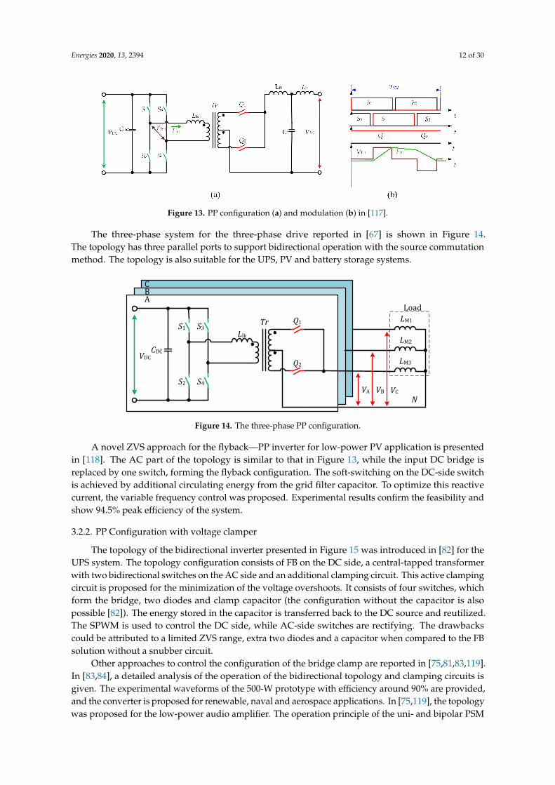
The topology in Figure 13a was introduced in [103] for the UPS. The topology utilizes the centraltapped transformer and two bidirectional switches at the AC side, while the DC side has a FB inverter.In [104], the converter was controlled with SPWM modulation at the DC side. In [99], an improvedmodulation method is introduced to handle the non-unity power factor without snubbers. A noveldigital control using the bipolar double modulation wave was addressed in [108], which is shown inFigure 13b. The sinusoidal output voltage is formed by AC-side semiconductors using PSM. It allowsachieving the ZVS turn-on on the DC side, and the ZVS turn-off at the AC side. The experimentalverification of the topology was presented using an experimental 250-W prototype with and 46-V outputvoltage. In [96], the topology with four additional snubber capacitors for switches S1-S4 is presented.The aim is to achieve the ZVS and ZCS in all semiconductor devices using PSM. The experimentalwaveforms of the prototype with 24-V input voltage and transformer 1:2.74 are shown. Anotherversion of the PSM is used in [115] to achieve the ZVS in the topology, which was confirmed with a1-kW experimental setup. Reference [116] presents the unidirectional converter for PV application,which utilizes the additional two inductors at the AC side.
Energies 2020, 13, 2394 12 of 30
Figure 13. PP configuration (a) and modulation (b) in [117].
The three-phase system for the three-phase drive reported in [67] is shown in Figure 14.The topology has three parallel ports to support bidirectional operation with the source commutationmethod. The topology is also suitable for the UPS, PV and battery storage systems.
Load
Q1
Q2
VA
Tr LM1S1 S3
VDCCDC
S2 S4
Llk
CBA
VB VC
LM2
LM3
N
Figure 14. The three-phase PP configuration.
A novel ZVS approach for the flyback—PP inverter for low-power PV application is presentedin [118]. The AC part of the topology is similar to that in Figure 13, while the input DC bridge isreplaced by one switch, forming the flyback configuration. The soft-switching on the DC-side switchis achieved by additional circulating energy from the grid filter capacitor. To optimize this reactivecurrent, the variable frequency control was proposed. Experimental results confirm the feasibility andshow 94.5% peak efficiency of the system.
3.2.2. PP Configuration with voltage clamper
The topology of the bidirectional inverter presented in Figure 15 was introduced in [82] for theUPS system. The topology configuration consists of FB on the DC side, a central-tapped transformerwith two bidirectional switches on the AC side and an additional clamping circuit. This active clampingcircuit is proposed for the minimization of the voltage overshoots. It consists of four switches, whichform the bridge, two diodes and clamp capacitor (the configuration without the capacitor is alsopossible [82]). The energy stored in the capacitor is transferred back to the DC source and reutilized.The SPWM is used to control the DC side, while AC-side switches are rectifying. The drawbackscould be attributed to a limited ZVS range, extra two diodes and a capacitor when compared to the FBsolution without a snubber circuit.
Other approaches to control the configuration of the bridge clamp are reported in [75,81,83,119].In [83,84], a detailed analysis of the operation of the bidirectional topology and clamping circuits isgiven. The experimental waveforms of the 500-W prototype with efficiency around 90% are provided,and the converter is proposed for renewable, naval and aerospace applications. In [75,119], the topologywas proposed for the low-power audio amplifier. The operation principle of the uni- and bipolar PSM

Energies 2020, 13, 2394 13 of 30
strategy is described and verified. In [81], an alternative bipolar PWM is proposed. It is suggested toallow achieving lower voltage distortion of the output compared to the unipolar PWM.
Figure 15. PP configuration with voltage clamper (a) and modulation (b) in [83].
3.2.3. PP Configuration with the Current Clamping Switch
The topology presented in Figure 16 [120–122] uses a standard full-bridge at the DC side. However,the AC side is realized with a center-tapped transformer and three bidirectional switches. In the originalpaper, the AC side structure was described as “three bidirectional switching arms” and referred to asPP configuration with the current clamping switch in this review due to the topology configuration.The DC side FB converts the DC voltage to the HF AC square wave. On the AC side, the switchingsignals are obtained by comparing the modulating waveform with the sawtooth carrier waveform.The bidirectional switch Q3 connected to the center tap is turned on when both Q1 and Q2 are in theoff-state to provide a freewheeling path for the output current. The additional overlap is added torealize the natural commutation of semiconductor devices and reduce overvoltage. The converterrealizes ZVS and ZCS for the semiconductor switches and requires three bidirectional switches insteadof four for the FB–FB topology. The bidirectional operation capability is reported, but not addressed.
Figure 16. PP configuration with the current clamping switch (a) and modulation (b) in [121].
Other versions of the topology for the bidirectional battery charger are reported in [85]. It utilizesthree bidirectional switches with regenerative flyback clamp circuit at the AC side, while the DC sideis FB. The presence of the clamping circuit allows the reduction of the voltage overshoot in AC andalso helps to achieve the ZCS in the AC switches. The energy stored in the clamp capacitor is returnedto the DC side and reused. The unipolar SPWM modulation strategy is used for both power transferdirections. The concept is verified with a 1.5-kW prototype with a 96% peak efficiency conversion from300-V battery to the 120-V RMS grid.
3.3. Resonant PP Topologies
PP Configuration with a Parallel Resonant Tank at the DC Side
In [80], the sine AM modulation (SAM) was proposed as an alternative approach for theconventional PWM with varied duty cycles. The topology consists of the PP configuration at theAC side and the FB with the parallel resonant tank at the DC side (Figure 17). The resonant tank

Energies 2020, 13, 2394 14 of 30
is connected between the middle point of the bridge legs and the middle point of the input voltagesource. The bridge leg is operated with a varying duty cycle and a constant phase shift. The switchingfrequency of the converter is slightly higher than the resonant to extend the load independence andenable ZVS in the semiconductors.
Figure 17. PP configuration with a parallel resonant tank at the DC side.
The results are verified with a simulation model of a 2-kW converter. The converters with theparallel and with the series resonant tank were analyzed for the connection 450-V DC source with theutility grid. It is shown that the topology in Figure 17 has lower efficiency than the voltage sourceversion on the topology with the series resonant tank, which will be described later.
The resonant inverter based on the topology from Figure 13 was introduced in [123,124] anddescribed in more detail in [125]. It uses a resonant capacitor in series to the leakage inductance.The topology is proposed for the UPS application and features a lower output voltage ripple. It allowssoft switching in the semiconductors using the SPWM modulation applied for FB thanks to thepresence of the resonant tank at the DC side. The AC-side switches are forming, working at the gridAC waveforms.
4. VSI Based Topologies
This section presents the topologies of the isolated matrix inverters with a grid side switchingstage based on the VSI. The subsections are organized according to the fourth hierarchical level of theclassification from Figure 5.
4.1. Non-Resonant Bridge Topologies
4.1.1. FB Configuration
Many different configurations of the VSI-based converters have been reported (also known as adual active bridge) [55,56,77,125–136]. In [105], the topology consists of two voltage source full-bridges,as shown in Figure 18. The advanced modulation strategy proposed is based on the triple-phase shift.The method allows for achieving soft-switching in a wide range of voltage and load. The experimental300-W prototype microinverter for the integration of the low-voltage DC source to the AC confirmedtheoretical descriptions in that work. The authors proposed the extension of this configuration for the3-port converter. In this case, in the first port is the PV module, the second–a battery and the third theAC grid. The connection of this part was made through the three-winding transformer. In general,the topology is suitable for different voltage levels, but the design of the high-frequency transformercan be a challenging part.
For the high-power applications, the VSI three-phase topologies can also be utilized (Figure 19).References [101,106,126–128] present PV inverter, battery storage and EV charger systems. In thosesystems, the PSM modulation strategy was used and is extended for the three-phase implementation.In [127], the three-port three-phase converter was proposed for interfacing between the renewablesource, battery and the utility grid controlled by PSM.

Energies 2020, 13, 2394 15 of 30
Figure 18. FB configuration.
Figure 19. Three-phase FB configuration.
4.1.2. HB Configuration
The bidirectional converter in Figure 20 is proposed for electric vehicle charging with powerfactor correction functionality [66,100]. The topology features a voltage source converter with twobidirectional switches and two capacitors on the AC side. At the DC side, a standard FB is applied.Additional inductors are supplied to both sides of the converter to reduce the current ripple. Thus,the DC side has the same number of switches, while the AC side has a twice reduced number ofswitches when compared to the FB–FB topology. The converter control algorithm is based on a generaltrapezoidal current mode modulation of the voltage source DC–DC converter and is operating witha combined phase shift and frequency modulation for shaping the transformer leakage inductancecurrent. This method is used to transfer high power with small peak current and achieve ZVS at anytime interval. Peak efficiency of 95% is obtained at half load for a 3.3-kW prototype and is claimedto potentially reach 97%, the value of efficiency depending on the battery voltage. At the same time,the converter requires rather complex multi-mode control with lookup tables to guarantee ZVS withinthe full range of operating conditions. The wide ratio of operating frequencies (1:6) imposes additionalrequirements on the design of passive elements. In practical systems, the efficiency is limited sincecertain minimum commutation current is required to guarantee ZVS over the whole AC grid cycle.The aim was to design a converter suitable for the medium/high voltage battery energy system. In thiscase, the converter submodules are connected per phase in series and share one filter inductance.
Figure 20. HB configuration (a) and modulation (b) in [66].

Energies 2020, 13, 2394 16 of 30
In [128], a 3-phase HB configuration of the VSI is proposed for the bidirectional conversionbetween the renewable source and the grid using the novel PSM modulation for the converter.
4.2. Resonant Bridge Topologies
4.2.1. FB Configuration with the Series Resonant Tank
Application of the series resonant FB inverter is shown in Figure 21 [60,129]. A converter for thephotovoltaic application was proposed and verified in [60]. The converter consists of two full-bridgesand transformer leakage inductance with the resonance capacitor forming the series resonant tank.As a result, the DC side PSM strategy and resonant tank allow achieving the soft switching in all devices.In [129], the topology was reported as the bidirectional charger for the electric vehicle. The converteroperation is similar to that previously discussed, but it is shown for both power flow directions: fromthe grid to electric vehicle and back.
Figure 21. FB configuration with the series resonant tank (a) and modulation (b) in [60].
4.2.2. FB Configuration with the Series Resonant Tank and HB at the DC Side
The topology in Figure 22 is a FB topology with the series resonant tank and HB DC side, which isdescribed in detail in [130] and proposed for UPS. The inverter uses the modulation of the DC side andallows achieving quasi ZCS on the switches. A small-scale converter prototype was shown, along withexperimental waveforms with linear and nonlinear loads. As the drawback of the topology is thatthe current in the DC-side switches is higher compared to the FB–FB converter, the topology is moresuitable for low-power applications.
Figure 22. FB configuration with the series resonant tank and HB at the DC side.
4.2.3. HB Configuration with the Series Resonant Tank
The circuit (Figure 23) for a PV microinverter is presented in [86]. The topology is based on a seriesresonant inverter at the DC side and HB voltage-doubler configuration at the AC side. The specialdual-phase shift modulation strategy for the topology allows achieving ZVS for all semiconductors.The experimental prototype for the integration of the low-voltage DC to AC grid with almost 96% CECefficiency was shown.

Energies 2020, 13, 2394 17 of 30
Figure 23. HB with the series resonant tank (a) and modulation (b) in [86].
An alternative version of the topology is addressed in [102]. The topology has similarity withFigure 23, but does not contain the resonant tank and blocking capacitor. Instead, the additional snubbercapacitor at the AC side is used, which provides the current path and no overshoot from leakageenergy is present at the AC-side switches. The topology was built in gallium nitride (GaN) switchesand used the dual-phase shift with variable frequency modulation to achieve ZVS. The hardwareprototype is shown to have the rectification from 230-V AC to 48-V DC. The topology is also capable ofDC AC conversion; however, this operation is not described.
4.2.4. HB Configuration with the Series Resonant Tank and HB at the DC Side
The converter in Figure 24 is recommended for an electric vehicle battery charger [107,131].The topology utilizes resonant HB with an active shunt circuit, which absorbs the current ripple at theDC side. In addition, at the AC side, the HB configuration is used. The presence of the active filter atthe DC side allows the reduction of the double grid frequency ripple in the current and reduces theoverheating of the battery. A special four-part control PSM strategy is proposed for the system, whichallows operation with different power ranges and achieving ZVS for all semiconductors.
In [132], a variation of this topology is suggested for the on-board electric vehicle charger.This converter includes the resonant tank and additional boost–buck stage for the additional gain onthe DC side, while the AC side is an HB. The topology does not require a bulky DC link between theboost–buck stage and the inverter stage. The authors proposed the harmonic modulation strategy,which allows improving the power factor in DCM. The 3-kW experimental bidirectional prototype wasbuilt with an efficiency of 93% at rated power.
Figure 24. HB configuration with the series resonant tank and HB at the DC side for the electric vehiclebattery charger.
4.3. Resonant PP Topologies
PP Configuration with the Series Resonant Tank
In [80], a topology consisting of the PP configuration at the AC side and the FB with the seriesresonant tank at the DC side is described (Figure 25). The series resonant tank is connected between the

Energies 2020, 13, 2394 18 of 30
middle point of the bridge legs, transformer AC sidewinding and the middle point of the input voltagesource. The SAM modulation for the DC side semiconductors is presented. The 2-kW simulationmodel of the inverter was made for the connection 450-V DC source with the utility grid. Resultingfrom the comparative analysis in the paper, this topology has lower energy circulation, but higherTHD, particularly at low power when compared to the CSI version of the topology in Figure 17 withthe parallel resonant tank.
Figure 25. PP configuration with the series resonant tank.
5. Discussion and Future Trends
5.1. Critical Overview
An important contribution of this work is that it establishes the isolated matrix inverters as a classof true single-stage topologies separate from the quasi-single-stage class. This division is important asthe isolated matrix inverters can provide a wider range of features. Besides being the true single-stagesolution, these inverters have the following advantages:
• they could provide the soft switching in all semiconductor switches using specialmodulation strategies;
• in the voltage step-up applications, they avoid unreliable high-voltage electrolytic capacitor(s)with a limited lifetime and utilize much more reliable low-voltage electrolytic capacitor(s) for thefiltering of 100/120 Hz voltage ripple;
• their cost can be reduced considerably with the implementation of emerging bidirectionalmonolithic semiconductors or the ones with the reverse blocking capability.
The main disadvantage of the isolated matrix inverters compared to their two-stage counterpartsis their relatively narrow input DC voltage range, which limits their applicability in demandingapplications. Other disadvantages can be associated with the limitations of the general level oftechnologies rather than the concept itself. For example, the level of control complexity was notcompatible with the existing technology when the first topologies appeared around 30 years ago.This was holding back the adoption of these inverters for some time. Nowadays, available low-costmicrocontrollers can realize control of the isolated matrix inverters. Moreover, recent appearance ofnumerous two- and quasi-single-stage solutions had gained popularity despite even more complicatedcontrol. Therefore, the isolated matrix inverters can also be accepted by industry if sufficient awarenessis raised.
Among the two main families of topologies, the CSI based isolated matrix inverters attractedmore attention of researchers compared to the VSI based counterparts, which resulted in twice as manytopologies developed. It can be attributed to their use of conventional LC and LCL filters, which makesthem a logical replacement of two-stage counterparts with the same filter type. In both groups, aroundhalf of the reported topologies were developed in the last five years, which shows high activity in thisfield of research. Nevertheless, both converter groups demonstrate efficiency growth from roughly 90%in early works up to 96% in later developments. It is worth mentioning that the CSI based topologieshave demonstrated high efficiency in a wider range of applications. Most of the research was dedicatedto the bridge type isolated matrix inverters, where the most prominent example is the single-phase
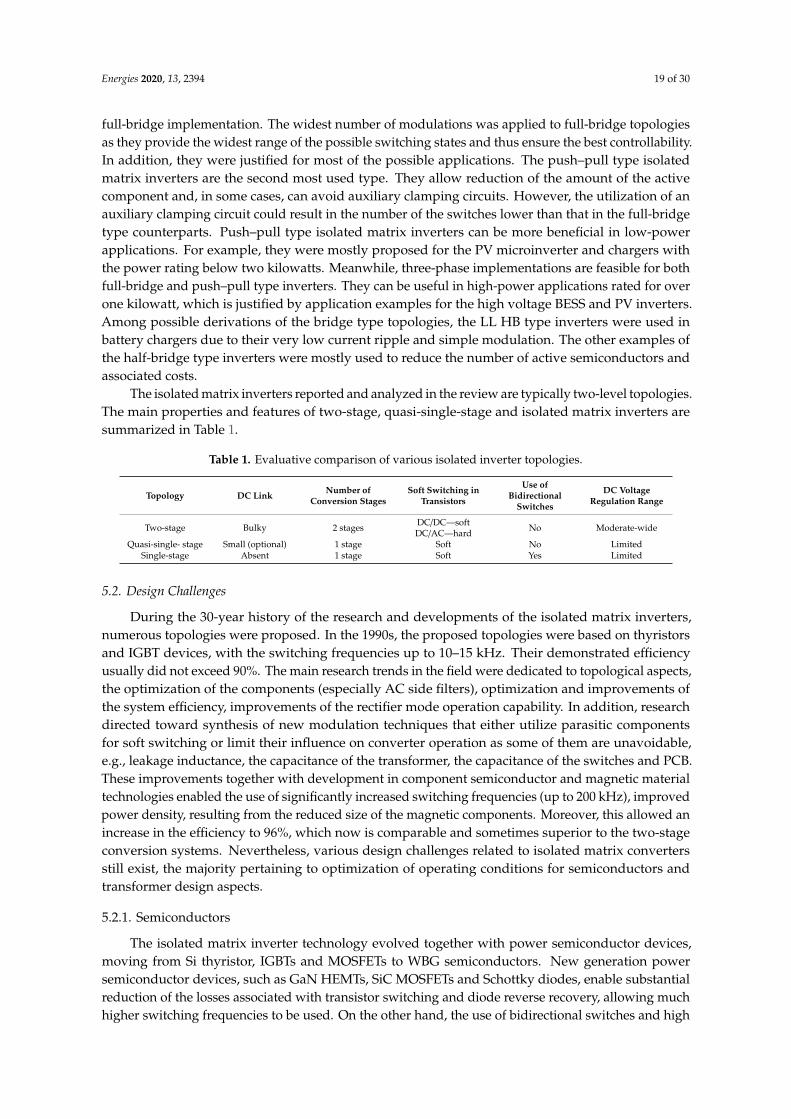
Energies 2020, 13, 2394 19 of 30
full-bridge implementation. The widest number of modulations was applied to full-bridge topologiesas they provide the widest range of the possible switching states and thus ensure the best controllability.In addition, they were justified for most of the possible applications. The push–pull type isolatedmatrix inverters are the second most used type. They allow reduction of the amount of the activecomponent and, in some cases, can avoid auxiliary clamping circuits. However, the utilization of anauxiliary clamping circuit could result in the number of the switches lower than that in the full-bridgetype counterparts. Push–pull type isolated matrix inverters can be more beneficial in low-powerapplications. For example, they were mostly proposed for the PV microinverter and chargers withthe power rating below two kilowatts. Meanwhile, three-phase implementations are feasible for bothfull-bridge and push–pull type inverters. They can be useful in high-power applications rated for overone kilowatt, which is justified by application examples for the high voltage BESS and PV inverters.Among possible derivations of the bridge type topologies, the LL HB type inverters were used inbattery chargers due to their very low current ripple and simple modulation. The other examples ofthe half-bridge type inverters were mostly used to reduce the number of active semiconductors andassociated costs.
The isolated matrix inverters reported and analyzed in the review are typically two-level topologies.The main properties and features of two-stage, quasi-single-stage and isolated matrix inverters aresummarized in Table 1.
Table 1. Evaluative comparison of various isolated inverter topologies.
Topology DC Link Number ofConversion Stages
Soft Switching inTransistors
Use ofBidirectional
Switches
DC VoltageRegulation Range
Two-stage Bulky 2 stages DC/DC—softDC/AC—hard No Moderate-wide
Quasi-single- stage Small (optional) 1 stage Soft No LimitedSingle-stage Absent 1 stage Soft Yes Limited
5.2. Design Challenges
During the 30-year history of the research and developments of the isolated matrix inverters,numerous topologies were proposed. In the 1990s, the proposed topologies were based on thyristorsand IGBT devices, with the switching frequencies up to 10–15 kHz. Their demonstrated efficiencyusually did not exceed 90%. The main research trends in the field were dedicated to topological aspects,the optimization of the components (especially AC side filters), optimization and improvements ofthe system efficiency, improvements of the rectifier mode operation capability. In addition, researchdirected toward synthesis of new modulation techniques that either utilize parasitic componentsfor soft switching or limit their influence on converter operation as some of them are unavoidable,e.g., leakage inductance, the capacitance of the transformer, the capacitance of the switches and PCB.These improvements together with development in component semiconductor and magnetic materialtechnologies enabled the use of significantly increased switching frequencies (up to 200 kHz), improvedpower density, resulting from the reduced size of the magnetic components. Moreover, this allowed anincrease in the efficiency to 96%, which now is comparable and sometimes superior to the two-stageconversion systems. Nevertheless, various design challenges related to isolated matrix convertersstill exist, the majority pertaining to optimization of operating conditions for semiconductors andtransformer design aspects.
5.2.1. Semiconductors
The isolated matrix inverter technology evolved together with power semiconductor devices,moving from Si thyristor, IGBTs and MOSFETs to WBG semiconductors. New generation powersemiconductor devices, such as GaN HEMTs, SiC MOSFETs and Schottky diodes, enable substantialreduction of the losses associated with transistor switching and diode reverse recovery, allowing muchhigher switching frequencies to be used. On the other hand, the use of bidirectional switches and high

Energies 2020, 13, 2394 20 of 30
number of discrete semiconductor components could discourage industrial adoption of the isolatedmatrix inverters. However, this number is in fact similar to that of industry-approved two-stage andquasi-single-stage solutions. Moreover, a new impulse for industrialization can be given by the recentdevelopments in monolithic reverse-blocking and bidirectional semiconductor devices that have beenreported for Si, SiC and GaN technologies [137–142]. This technology can make the isolated matrixinverters attractive to the industry by reducing the number of discrete devices by up to twofold at theAC side.
5.2.2. Isolation Transformer
The use of the HF transformers imposes challenges on the scalability of the isolated matrix inverters.The limiting factors are core losses (losses from eddy current and magnetic losses), high-frequency losses(skin and proximity effects and winding losses in the high current application), parasitic resonances(usually between the capacitance and leakage inductance of the transformer, but the topology hassome influence on it) [143]. Depending on the operating switching frequency, the impact of the totaltransformer losses in the total power loss will be different. For switching frequencies of up to a fewdozen kHz, GTOs and IGBTs are commonly utilized, which results in the dominant impact of theirswitching losses on the overall efficiency. At higher switching frequencies, where the implementation ofSi, SiC and GaN devices is favored, an increased impact of the transformer losses is expected. The softswitching range in the CSI based galvanically isolated matrix inverters is usually determined by thevalues of the transformer leakage inductance and parasitic capacitance. In the VSI based solutions,the value of the leakage inductance has an effect on regulation near the voltage zero-crossing point.The transformer power and turns ratio significantly influence the values of the parasitic parametersand, consequently, limit the overall efficiency. The scaling of the transformer is mostly defined bythe required power rating and power density. A compact design usually requires increasing theworking frequency but results in lower efficiencies. Finding the tradeoff between the target powerdensity and efficiency of an inverter may require an iterative search for the optimal topology as acompact transformer design could result in such a combination of switching frequency and the leakageinductance that may limit the feasibility of some of the topologies. The isolated matrix converterprototypes reported in the literature have been mainly using ferrite RM cores for powers <1 kW andtoroid or E cores for powers over one kilowatt. Improved transformer characteristics may be obtainedwith amorphous and nanocrystalline magnetic materials, which can result in core losses reduction byup to 70% than conventional solutions [144,145].
5.3. Application Examples
The practical realization of the isolated matrix inverters for a target application depends onthe engineering design and limitations of existing technologies of semiconductor and magneticcomponents. Hence, it is important to compile a comprehensive list of application examples withkey operating parameters to provide an initial suggestion regarding the suitability of a topology to acertain application. Therefore, application examples of the isolated matrix inverters were summarizedin Table 2 to provide a critical view of the practical value of each of the roughly thirty topologiesand support claims of this section. The comparison considers the number of switches on both sidesseparately, transformer turns ratio, maximum power and reported experimental efficiency, inputand output voltage level or range, switching frequency and the used modulation technique. As canbe seen from the table, the technology of isolated matrix inverters is a versatile solution that suitsdifferent applications.

Energies 2020, 13, 2394 21 of 30
Table 2. Summary of the existing solutions of the isolated matrix inverters.
AC Side-BasedTopology Reference Peak
EfficiencyYear Number of DC
Side SwitchesNumber of ACSide Switches
ModulationStrategy
The Ratio of HFTransformer Power, kW DC Voltage,
VAC Voltage,
Vrms
SwitchingFrequency,
kHzApplication
CSI-based
FB
[58] 89 1990 4 8 PSM – 1 180 100 20 UPS[46] – 2006 4 8 PSM 1:1 10 600 230 6 MVC[47] 96 2018 4 8 PWM 1:1 1.2 400 240 54 HF AC grid[51] 96.5 2018 4 8 PWM 1:1 1.2 300 120 50 –[52] – 2019 4 8 PSM 1:1.1 1.2 400 230 50 PV
FB withreconfig. output [62] 92.5 2010 4 16 PWM 2×1:6.5 1 30–60 120/240 – FC
FB 3-leg DC side [79] 95.1 2020 6 8 PSM – 0.34 34 240 25, 50 PV MIC*FB
3-phase[58] – 1990 4 12 PSM – 1 200 100 20 UPS[76] – 2006 4 12 PSM 1:1 40 600 230 6 MVC
HB [115] – 2011 4 4 PWM 3:13 1 36 98–100 20 PV MICLL HB [97] 96.5 2017 2 4 PSM 1:5 1.5 220–336 120 100 EVLL HB
3-phase [98] 2019 6 12 PSM 10 220–336 120 100 EV
PP3-phase [67] 89 2011 12 12 PWM – 1 90 90 ˇ 20 AC drive
PPresonant [80] – 2018 4 4 AM – 2 450 230 50 –
PP withvoltage clamper
[82] 88 1990 4 4+4(cl) PWM – 10 – 100 20 UPS[83] 90 2016 4 4+4(cl) PWM 24:23:8 1 60 100 20 –[75] 96 2016 4 4+4(cl*) PWM 1:4:4 0.08 10 25 ˇ 200 D AMP*[81] 93.5 2018 4 4+4(cl) PWM 7:7:20 0.2 340–370 40 200 –
PP withcurrentclamper
[112] – 2004 4 6 PWM 3:8 – 150 230 25 –[85] 96 2019 4 6+4(cl) PWM – 1.5 300 120 50 EV
VSI-based
FB [105] 91 2020 4 8 PSM 1:5 0.2 48 110 50 PV MICFB
resonant[60],[129] – 2011 4 16 PSM 1:6.5 1 30–60 120 100 PV, EV
HB[61] 94.5 2016 4 4 PSM 1:6:6 0.25 30–48 110 50 PV MIC
[127] – 2016 4 4 PSM + FM 1:1.3 3.3 280–420 230 20–120 EV
HBresonant
[132] 95.5 2014 4 4 FM 1:0.7 3 280–450 230/110 100 EV[86] 96 2010 4 4 PSM+FM 1:7.5 0.175 25–40 240 45–350 PV MIC
[131] – 2016 2+2(cl) 4 PSM – 3 400 230 60 EV
FB3-phase
[53] – 2018 4 12 PWM – 10 200 100 20 Batterystorage
[126] – 2012 4 12 PSM – 10 600 230 36 PVinverter
HB3-phase [127] – 2019 6+2(cl) 6 PSM 1:1 1.1 530 311 20 –
* PV MIC—PV microinverter, D AMP—D class audio amplifier, cl—additional clamping switch ˇ—from oscillograms

Energies 2020, 13, 2394 22 of 30
It is worth mentioning that the compiled list of application examples is reflecting the currentstate-of-the-art and does not limit future applications. It could be expected that they can be used inmore electric aircraft [146], where conventional matrix converters were justified. Currently, only VSIbased solutions were adopted by industry for PV microinverter applications. However, in the lastfew years, early attempts of industrialization of the CSI based isolated matrix inverters have emerged.For example, “ACDC cube” project of INESC TEC in Portugal [147]. More commercial productsemploying CSI based solutions can be expected in the future. This paper aims to facilitate its widerindustrial acceptance.
6. Conclusions
This paper provides a fresh view of existing galvanically isolated inverters and establishes theirdivision into three main classes: two-stage, quasi-single-stage and single-stage. The superiority offeatures provided by the single-stage solutions makes the isolated matrix inverters a promising solution.Currently, over thirty topologies have been reported where two-thirds belong to the group based oncurrent-source inverters. They have attracted more research interest as the logical replacement oftwo-stage solutions with the same LC or LCL grid side filter. Nevertheless, the VSI-based topologiescan demonstrate equally high efficiencies of 96% and have been industrialized already in the PVmicroinverter applications. Regardless of the basic inverter topology, full-bridge solutions are themost popular due to their high control and modulation flexibility. This trend is expected to continuein the future, but push–pull converters with voltage or current clamping will also gain momentumin development.
Vast majority of the topologies presented in this review were found to use either PWM orPSM. The CSI-based isolated matrix inverters are using PWM twice as often as PSM. However,both modulations have shown the capability of achieving 96.5% efficiency under similar operationparameters. At the same time, the voltage source-based topologies are using PSM three times moreoften than PWM. Here, PSM showed better efficiency levels than in the case of PWM mainly due toutilization of more than one phase shift. More sophisticated methods additionally apply FM to obtaineven better characteristics.
The suggested range of existing applications is wide, but most of the topologies were proposedfor photovoltaic, battery energy storage, electric vehicle charging and uninterruptible power supplyapplications. Less common applications include D class audio amplifiers, adjustable speed drives,medium voltage converters, fuel cells and local high-frequency AC grid forming. This proves theversatility of the isolated matrix inverters and shows that much wider application areas can be expectedto appear in the near future.
Future research is expected to be focused on the development of new modulation techniques(mostly based on PWM and PSM), voltage range extension at the DC side, optimization of componentsizes (especially AC side filter), experimental validation of benefits of the isolated matrix invertersin new applications (e.g., more electric aircraft, electric transportation, grid-connected rectifiers,etc.). Another important research topic relevant to industrial acceptance lies in the accumulation ofadditional knowledge in control and regulation methods for these inverters. For example, it is requiredto investigate the use of isolated matrix inverters in reactive power regulation, power quality and gridcode compatibility potential, including fault ride-through capabilities.
Author Contributions: Conceptualization, O.K. and A.B.; writing—original draft preparation, O.K. and A.B.;writing—review and editing, D.V. and A.C.; supervision, A.B and D.V.; funding acquisition, A.B and D.V. Allauthors have read and agreed to the published version of the manuscript.
Funding: The preparing of this publication was supported in part by the EEA/Norway Financial Mechanism2014–2021 under Grant EMP474 and in part by the Estonian Centre of Excellence in Zero Energy and ResourceEfficient Smart Buildings and Districts, ZEBE, grant 2014–2020.4.01.15–0016 funded by the European RegionalDevelopment Fund.
Conflicts of Interest: The authors declare no conflict of interest.
Energies 2020, 13, 2394 23 of 30
References
1. Child, M.; Koskinen, O.; Linnanen, L.; Breyer, C. Sustainability guardrails for energy scenarios of the globalenergy transition. Renew. Sustain. Energy Rev. 2018, 91, 321–334. [CrossRef]
2. O’Neill, B.C.; Oppenheimer, M. CLIMATE CHANGE: Dangerous Climate Impacts and the Kyoto Protocol.Science 2002, 296, 1971–1972. [CrossRef] [PubMed]
3. Rosen, A.M. The Wrong Solution at the Right Time: The Failure of the Kyoto Protocol on Climate Change.Politics Policy 2015, 43, 30–58. [CrossRef]
4. Savaresi, A. The Paris Agreement: A new beginning? J. Energy Nat. Resour. Law 2016, 34, 16–26. [CrossRef]5. Verbic, M.; Filipovic, S.; Radovanovic, M. Electricity prices and energy intensity in Europe. Util. Policy 2017,
47, 58–68. [CrossRef]6. Rockström, J.; Gaffney, O.; Rogelj, J.; Meinshausen, M.; Nakicenovic, N.; Schellnhuber, H.J. A roadmap for
rapid decarbonization. Science 2017, 355, 1269–1271. [CrossRef]7. Al Irsyad, M.I.; Halog, A.; Nepal, R. Renewable energy projections for climate change mitigation: An analysis
of uncertainty and errors. Renew. Energy 2019, 130, 536–546. [CrossRef]8. IRENA. Global Energy Transformation: A Roadmap to 2050, 2019 ed.; International Renewable Energy Agency:
Abu Dhabi, UAE, 2019; ISBN 978-92-9260-121-8.9. IRENA. Electrification with Renewables: Driving the Transformation of Energy Services; International Renewable
Energy Agency: Abu Dhabi, UAE, 2019; ISBN 97.10. Kassakian, J.G.; Jahns, T.M. Evolving and Emerging Applications of Power Electronics in Systems. IEEE J.
Emerg. Sel. Top. Power Electron. 2013, 1, 47–58. [CrossRef]11. Blaabjerg, F.; Chen, Z.; Kjaer, S. Power Electronics as Efficient Interface in Dispersed Power Generation
Systems. IEEE Trans. Power Electron. 2004, 19, 1184–1194. [CrossRef]12. Ellabban, O.; Abu-Rub, H.; Blaabjerg, F. Renewable energy resources: Current status, future prospects and
their enabling technology. Renew. Sustain. Energy Rev. 2014, 39, 748–764. [CrossRef]13. Jager-Waldau, A.; Bodis, K.; Kougias, I.; Szabo, S. The New European Renewable Energy
Directive—Opportunities and Challenges for Photovoltaics. In Proceedings of the 2019 IEEE 46th PhotovoltaicSpecialists Conference (PVSC), Chicago, IL, USA, 16–21 June 2019; pp. 592–594.
14. Zervos, A.; Lins, C.; Muth, J. RE-thinking 2050: A 100% Renewable Energy Vision for the European Union;European Renewable Energy Council: Brussels, Belgium, 2010.
15. Jacobson, M.Z.; Delucchi, M.A.; Bauer, Z.A.; Goodman, S.C.; Chapman, W.E.; Cameron, M.; Bozonnat, C.;Chobadi, L.; Clonts, H.A.; Enevoldsen, P.; et al. 100% Clean and Renewable Wind, Water, and SunlightAll-Sector Energy Roadmaps for 139 Countries of the World. Joule 2017, 1, 108–121. [CrossRef]
16. Lazaroiu, G.C.; Roscia, M. Blockchain and smart metering towards sustainable prosumers. In Proceedingsof the 2018 International Symposium on Power Electronics, Electrical Drives, Automation and Motion(SPEEDAM), Amalfi, Italy, 20–22 June 2018; pp. 550–555. [CrossRef]
17. Bindra, A. Projecting the Evolution of Power Electronics: Highlights from FEPPCON VIII. IEEE PowerElectron. Mag. 2016, 3, 32–44. [CrossRef]
18. Kurnitski, J.; Saari, A.; Kalamees, T.; Vuolle, M.; Niemelä, J.; Tark, T. Cost optimal and nearly zero(nZEB) energy performance calculations for residential buildings with REHVA definition for nZEB nationalimplementation. Energy Build. 2011, 43, 3279–3288. [CrossRef]
19. Zafar, S.; Dincer, I. Energy, exergy and exergoeconomic analyses of a combined renewable energy system forresidential applications. Energy Build. 2014, 71, 68–79. [CrossRef]
20. Cetin, E.; Yilanci, A.; Ozturk, H.K.; Colak, M.; Kasikci, I.; Iplikci, S. A micro-DC power distribution systemfor a residential application energized by photovoltaic–wind/fuel cell hybrid energy systems. Energy Build.2010, 42, 1344–1352. [CrossRef]
21. Gomis-Bellmunt, O.; Sau-Bassols, J.; Prieto-Araujo, E.; Cheah-Mane, M. Flexible Converters for MeshedHVDC Grids: From Flexible AC Transmission Systems (FACTS) to Flexible DC Grids. IEEE Trans. PowerDeliv. 2020, 35, 2–15. [CrossRef]
22. Dong, N.; Cvetkovic, I.; Boroyevich, D.; Zhang, W.; Wang, R.; Mattavelli, P. Grid-Interface BidirectionalConverter for Residential DC Distribution Systems—Part One: High-Density Two-Stage Topology. IEEETrans. Power Electron. 2012, 28, 1655–1666. [CrossRef]

Energies 2020, 13, 2394 24 of 30
23. Aamir, M.; Kalwar, K.A.; Mekhilef, S. Review: Uninterruptible Power Supply (UPS) system. Renew. Sustain.Energy Rev. 2016, 58, 1395–1410. [CrossRef]
24. Stecca, M.; Elizondo, L.R.; Soeiro, T.B.; Bauer, P.; Palensky, P. A Comprehensive Review of the Integrationof Battery Energy Storage Systems into Distribution Networks. IEEE Open J. Ind. Electron. Soc. 2020, 1.[CrossRef]
25. Sarlioglu, B.; Morris, C.T.; Han, D.; Li, S. Driving Toward Accessibility: A Review of TechnologicalImprovements for Electric Machines, Power Electronics, and Batteries for Electric and Hybrid Vehicles. IEEEInd. Appl. Mag. 2016, 23, 14–25. [CrossRef]
26. Jiang, Y.; Liu, J.; Tian, W.; Shahidehpour, M.; Krishnamurthy, M. Energy Harvesting for the Electrification ofRailway Stations: Getting a charge from the regenerative braking of trains.A. IEEE Electrif. Mag. 2014, 2,39–48. [CrossRef]
27. Saidur, R.; Mekhilef, S.; Ali, M.; Safari, A.; Mohammed, H.A. Applications of variable speed drive (VSD) inelectrical motors energy savings. Renew. Sustain. Energy Rev. 2012, 16, 543–550. [CrossRef]
28. Zhong, Q.-C. Virtual Synchronous Machines: A unified interface for grid integration. IEEE Power Electron.Mag. 2016, 3, 18–27. [CrossRef]
29. Carrasco, J.; Franquelo, L.G.; Bialasiewicz, J.; Galvan, E.; Portillo, R.; Prats, M.; Ángeles, M.; Leon, J.I.;Moreno-Alfonso, N. Power-Electronic Systems for the Grid Integration of Renewable Energy Sources:A Survey. IEEE Trans. Ind. Electron. 2006, 53, 1002–1016. [CrossRef]
30. Trintis, I.; Teodorescu, R.; Munk-Nielsen, S. Single stage grid converters for battery energy storage.In Proceedings of the 5th IET International Conference on Power Electronics, Machines and Drives (PEMD2010), Brighton, UK, 19–21 April 2010; pp. 1–6.
31. Kouro, S.; Leon, J.I.; Vinnikov, D.; Franquelo, L.G. Grid-Connected Photovoltaic Systems: An Overview ofRecent Research and Emerging PV Converter Technology. IEEE Ind. Electron. Mag. 2015, 9, 47–61. [CrossRef]
32. Takaoka, N.; Watanabe, H.; Itoh, J.-I. Isolated DC to Single-phase AC Converter with Active Power DecouplingCapability for Battery Storage System. In Proceedings of the 2019 8th International Conference on RenewableEnergy Research and Applications (ICRERA), Brasov, Romania, 3–6 November 2019; pp. 739–743.
33. Wu, H.; Jia, Y.; Yang, F.; Zhu, L.; Xing, Y. Two-Stage Isolated Bidirectional DC-AC Converters With Three-PortConverters and Two DC-Buses. IEEE J. Emerg. Sel. Top. Power Electron. 2020, 1. (early access). [CrossRef]
34. Xuewei, P.; Rathore, A.K.; Prasanna, U.R. Novel Soft-Switching Snubberless Naturally Clamped Current-FedFull-Bridge Front-End-Converter-Based Bidirectional Inverter for Renewables, Microgrid, and UPSApplications. IEEE Trans. Ind. Appl. 2014, 50, 4132–4141. [CrossRef]
35. Hanchao, Z.; Daolian, C. A single-stage isolated charging/discharging DC-AC converter with secondharmonic current suppression in distributed generation systems. In Proceedings of the IECON 2017—43rdAnnual Conference of the IEEE Industrial Electronics Society, Beijing, China, 29 October–1 November 2017;pp. 4427–4432.
36. Everts, J.; Krismer, F.; Keybus, J.V.D.; Driesen, J.; Kolar, J.W. Optimal ZVS Modulation of Single-PhaseSingle-Stage Bidirectional DAB AC–DC Converters. IEEE Trans. Power Electron. 2013, 29, 3954–3970.[CrossRef]
37. Wang, K.; Lee, F.; Dong, W. A new soft-switched quasi-single-stage (QSS) bi-directional inverter/charger. InProceedings of the Conference Record of the 1999 IEEE Industry Applications Conference. Thirty-Forth IASAnnual Meeting (Cat. No.99CH36370), Phoenix, AZ, USA, 3–7 October 1999; Volume 4, pp. 2031–2038.
38. Cuadros, C.; Chandrasekaran, S.; Wang, K.; Boroyevich, D.; Lee, F. Modeling, control and implementationof the quasi-single stage three-phase zero-voltage zero-current switched buck rectifier. In Proceedings ofthe APEC ’99. Fourteenth Annual Applied Power Electronics Conference and Exposition. 1999 ConferenceProceedings (Cat. No.99CH36285), Dallas, TX, USA, 14–18 March 1999; Volume 1, pp. 248–254.
39. De, D.; Ramanarayanan, V. Analysis, Design, Modeling, and Implementation of an Active Clamp HF LinkConverter. IEEE Trans. Circuits Syst. I: Regul. Pap. 2011, 58, 1446–1455. [CrossRef]
40. Wang, Z.; Zhang, Y.; You, S.; Xiao, H.; Cheng, M. An Integrated Power Conversion System for ElectricTraction and V2G Operation in Electric Vehicles With a Small Film Capacitor. IEEE Trans. Power Electron.2020, 35, 5066–5077. [CrossRef]
41. Chakraborty, S.; Chattopadhyay, S. A Dual-Active-Bridge-Based Fully ZVS HF-Isolated Inverter With LowDecoupling Capacitance. IEEE Trans. Power Electron. 2020, 35, 2615–2628. [CrossRef]

Energies 2020, 13, 2394 25 of 30
42. Li, X.; Bhat, A.K.S. A Comparison Study of High-Frequency Isolated DC/AC Converter Employing anUnfolding LCI for Grid-Connected Alternative Energy Applications. IEEE Trans. Power Electron. 2014, 29,3930–3941. [CrossRef]
43. Mazumder, S.K.; Burra, R.; Huang, R.; Tahir, M.; Acharya, K.; Garcia, G.; Pro, S.; Rodrigues, O.;Stasinopoulos, M. Single-stage low-cost and energy-efficient isolated phase-shifted high-frequency inverterfollowed by a forced cycloconverter for universal residential fuel cell power system. In Proceedings of the2008 IEEE International Conference on Electro/Information Technology, Ames, IA, USA, 18–20 May 2008;pp. 408–413.
44. Pal, A.; Basu, K. A unidirectional snubber less fully soft-switched single stage three phase high frequency linkDC/AC converter. In Proceedings of the 2017 IEEE 3rd International Future Energy Electronics Conferenceand ECCE Asia (IFEEC 2017—ECCE Asia), Kaohsiung, Taiwan, 3–7 June 2017; pp. 1777–1784.
45. Moschopoulos, G.; Liu, Y.; Bassan, S. AC-DC quasi-single-stage converters. In Proceedings of theINTELEC—29th International Telecommunications Energy Conference, Rome, Italy, 30 September–4 October2007; pp. 498–505.
46. Norrga, S. Experimental Study of a Soft-Switched Isolated Bidirectional AC DC Converter Without AuxiliaryCircuit. IEEE Trans. Power Electron. 2006, 21, 1580–1587. [CrossRef]
47. Wang, M.; Guo, S.; Huang, Q.; Yu, W.; Huang, A.Q. An Isolated Bidirectional Single-Stage DC–ACConverter Using Wide-Band-Gap Devices With a Novel Carrier-Based Unipolar Modulation TechniqueUnder Synchronous Rectification. IEEE Trans. Power Electron. 2017, 32, 1832–1843. [CrossRef]
48. Muroyama, S.; Aoki, T.; Yotsumoto, K. A control method for a high frequency link inverter using cycloconvertertechniques. In Proceedings of the Conference Proceedings., Eleventh International TelecommunicationsEnergy Conference, Florence, Italy, 15–18 October 1989; Volume 2, p. 19.
49. Kummari, N.; Chakraborty, S.; Chattopadhyay, S. Chattopadhyay, Secondary side modulation of a single-stageisolated high-frequency link microinverter with a regenerative flyback snubber. In Proceedings of the 2016IEEE Energy Conversion Congress and Exposition (ECCE), Milwaukee, WI, USA, 18–22 September 2016;pp. 1–8.
50. Kummari, N.; Chakraborty, S.; Chattopadhyay, S. An Isolated High-Frequency Link Microinverter Operatedwith Secondary-Side Modulation for Efficiency Improvement. IEEE Trans. Power Electron. 2018, 33, 2187–2200.[CrossRef]
51. Nayak, P.; Rajashekara, K.; Pramanick, S. Soft-Switched Modulation Technique for a Single-Stage Matrix-TypeIsolated DC–AC Converter. IEEE Trans. Ind. Appl. 2019, 55, 7642–7656. [CrossRef]
52. Blinov, A.; Korkh, O.; Vinnikov, D.; Galkin, I.; Norrga, S. Soft-Switching Modulation Method for Full-BridgeDC-AC HF-Link Inverter. In Proceedings of the IECON 2019—45th Annual Conference of the IEEE IndustrialElectronics Society, Lisbon, Portugal, 14–17 October 2019; pp. 4417–4422.
53. Varajão, D.; Araújo, R.E.; Miranda, L.M.; Lopes, J.A.P. Modulation Strategy for a Single-Stage Bidirectionaland Isolated AC–DC Matrix Converter for Energy Storage Systems. IEEE Trans. Ind. Electron. 2018, 65,3458–3468. [CrossRef]
54. Wheeler, P.; Rodriguez, J.; Clare, J.; Empringham, L.; Weinstein, A. Matrix converters: A technology review.IEEE Trans. Ind. Electron. 2002, 49, 276–288. [CrossRef]
55. Yan, Z.; Xu, X.; Yang, Z.; Zhang, Q.; Wang, Y. A Novel SVM Control Strategy for a Single-Phase HighFrequency Link Matrix Rectifier. In Proceedings of the 2015 Fifth International Conference on Instrumentationand Measurement, Computer, Communication and Control (IMCCC), Qinhuangdao, China, 18–20 September2015; pp. 453–458.
56. Mei, Y.; Huang, W.; Liu, Z. Research on Control Strategy of Bidirectional Isolated AC/DC Matrix Converter.In Proceedings of the 2018 IEEE International Power Electronics and Application Conference and Exposition(PEAC), Shenzhen, China, 4–7 November 2018; pp. 1–4.
57. Mennicken, H. Stromrichtersystem Mit Wechselspannungs-Zwischenkreis Und Seine Anwendung in derTraktionstechnik. Ph.D. Thesis, RWTH Aachen University, Aachen, Germany, 1978.
58. Kawabata, T.; Honjo, K.; Sashida, N.; Sanada, K.; Koyama, M. High frequency link DC/AC converter withPWM cycloconverter. In Proceedings of the Conference Record of the 1990 IEEE Industry ApplicationsSociety Annual Meeting, Seattle, WA, USA, 7–12 October 1990; Volume 2, pp. 1119–1124.

Energies 2020, 13, 2394 26 of 30
59. Matsui, M.; Nagai, M.; Mochizuki, M.; Nabae, A. High-frequency link DC/AC converter with suppressedvoltage clamp circuits-naturally commutated phase angle control with self turn-off devices. IEEE Trans. Ind.Appl. 1996, 32, 293–300. [CrossRef]
60. Krishnaswami, H. Photovoltaic microinverter using single-stage isolated high-frequency link series resonanttopology. In Proceedings of the 2011 IEEE Energy Conversion Congress and Exposition, Phoenix, AZ, USA,17–22 September 2011; pp. 495–500.
61. Surapaneni, R.K.; Yelaverthi, D.B.; Rathore, A.K. Cycloconverter-Based Double-Ended MicroinverterTopologies for Solar Photovoltaic AC Module. IEEE J. Emerg. Sel. Top. Power Electron. 2016, 4, 1354–1361.[CrossRef]
62. Mazumder, S.K.; Burra, R.K.; Huang, R.; Tahir, M.; Acharya, K. A Universal Grid-Connected Fuel-CellInverter for Residential Application. IEEE Trans. Ind. Electron. 2010, 57, 3431–3447. [CrossRef]
63. Krein, P.; Balog, R.; Geng, X. High-Frequency Link Inverter for Fuel Cells Based on Multiple-Carrier PWM.IEEE Trans. Power Electron. 2004, 19, 1279–1288. [CrossRef]
64. Iyer, K.; Mohan, N. Modulation and Commutation of a Single Stage Isolated Asymmetrical MultilevelConverter for Integration of Renewables and Battery Energy Storage System in Ships. IEEE Trans. Transp.Electrif. 2016, 2, 1. [CrossRef]
65. Norrga, S. A soft-switched bi-directional isolated AC/DC converter for AC-fed railway propulsion applications.In Proceedings of the 2002 International Conference on Power Electronics, Machines and Drives, Sante Fe,NM, USA, 4–7 June 2002; pp. 433–438.
66. Jauch, F.; Biela, J. Single-phase single-stage bidirectional isolated ZVS AC-DC converter with PFC. InProceedings of the 2012 15th International Power Electronics and Motion Control Conference (EPE/PEMC),Novi Sad, Serbia, 4–6 September 2012.
67. Basu, K.; Mohan, N. A High-Frequency Link Single-Stage PWM Inverter With Common-Mode VoltageSuppression and Source-Based Commutation of Leakage Energy. IEEE Trans. Power Electron. 2013, 29,3907–3918. [CrossRef]
68. Alluhaybi, K.; Batarseh, I.; Hu, H.; Chen, X. Comprehensive Review and Comparison of Single-PhaseGrid-Tied Photovoltaic Microinverters. IEEE J. Emerg. Sel. Top. Power Electron. 2020, 8, 1310–1329. [CrossRef]
69. Fornage, M.; Hassan-Ali, M.; Omar, T.H. Method and Apparatus for Providing Power Conversion Usingan Interleaved Flyback Converter with Automatic Balancing. Patent EP2043246A2, 2007. Available online:https://patents.google.com/patent/EP2043246A2/ru (accessed on 9 May 2020).
70. Harrison, M.J.; Zimmanck, D.R. Single-Phase Cycloconverter with Integrated Line-Cycle Energy Storage.Patent WO2015038995A1, 2014. Available online: https://patents.google.com/patent/WO2015038995A1/en?oq=WO2015038995A1 (accessed on 9 May 2020).
71. Kimball, J.W.; Krein, P.T.; Benavides, N.D. Modular System for Unattended Energy Generation and Storage.Patent US8350411B2, 2006. Available online: https://patents.google.com/patent/US8350411B2/en (accessedon 9 May 2020).
72. Kwon, O.; Kim, J.; Kwon, J.-M.; Kwon, B.-H. Bidirectional Grid-Connected Single-Power-ConversionConverter With Low-Input Battery Voltage. IEEE Trans. Ind. Electron. 2017, 65, 3136–3144. [CrossRef]
73. Chen, W.W.; Zane, R.; Corradini, L. Isolated Bidirectional Grid-Tied Three-Phase AC–DC Power ConversionUsing Series-Resonant Converter Modules and a Three-Phase Unfolder. IEEE Trans. Power Electron. 2017, 32,9001–9012. [CrossRef]
74. Diogo, A.C.P.B.V.; Luís, M.F.M.; Rui, M.E.A. Single-Phase Cycloconverter with Integrated Line-Cycle EnergyStorage. Patent US9973107B2, 2015. Available online: https://patents.google.com/patent/US9973107B2/en(accessed on 9 May 2020).
75. Guo, S.; Su, J.; Guo, L.; Chen, X. Phase-shifted modulation strategies for a single-stage isolated bi-directionalpower amplifier. In Proceedings of the 2016 IEEE 8th International Power Electronics and Motion ControlConference (IPEMC-ECCE Asia), Hefei, China, 22–26 May 2016; pp. 1206–1211.
76. Norrga, S.; Meier, S.; Ostlund, S. A three-phase soft-switched isolated AC/DC converter without auxiliarycircuit. IEEE Trans. Ind. Appl. 2004, 44, 836–844. [CrossRef]
77. Vangen, K.; Melaa, T.; Bergsmark, S.; Nilsén, R. Efficient high-frequency soft-switched power converterwith signal processor control. In Proceedings of the Thirteenth International Telecommunications EnergyConference—INTELEC 91, Kyoto, Japan, 5–8 November 1991; pp. 631–639.

Energies 2020, 13, 2394 27 of 30
78. Aganza-Torres, A.; Cardenas, V. Analysis and modelling of HF-Link Cycloconverter based inverter forlow-power renewable energy sources applications. In Proceedings of the 2011 8th International Conferenceon Electrical Engineering, Computing Science and Automatic Control, Merida City, Mexico, 26–28 October2011; pp. 1–6.
79. Kummari, N.; Chattopadhyay, S. Three-Legged High-Gain Phase-Modulated DC–AC Converter for Mitigationof Device Capacitance Induced Ringing Voltage. IEEE Trans. Power Electron. 2020, 35, 1306–1321. [CrossRef]
80. Knabben, G.C.; Neumayr, D.; Kolar, J.W. Constant duty cycle sinusoidal output inverter with sine amplitudemodulated high frequency link. In Proceedings of the 2018 IEEE Applied Power Electronics Conference andExposition (APEC), San Antonio, TX, USA, 4–8 March 2018; pp. 2521–2529.
81. Zhou, X.; Xu, J.; Zhong, S. Single-Stage Soft-Switching Low-Distortion Bipolar PWM ModulationHigh-Frequency-Link DC–AC Converter With Clamping Circuits. IEEE Trans. Ind. Electron. 2018,65, 7719–7729. [CrossRef]
82. Yamato, I.; Tokunaga, N.; Matsuda, Y.; Suzuki, Y.; Amaro, H. High frequency link DC-AC converter forUPS with a new voltage clamper. In Proceedings of the 21st Annual IEEE Conference on Power ElectronicsSpecialists, San Antonio, TX, USA, 11–14 June 1990; pp. 749–756.
83. Zhu, W.; Zhou, K.; Cheng, M. A Bidirectional High-Frequency-Link Single-phase Inverter: Modulation,Modeling, and Control. IEEE Trans. Power Electron. 2013, 29, 4049–4057. [CrossRef]
84. Zhu, W.; Zhou, K.; Cheng, M.; Peng, F. A High-Frequency-Link Single-Phase PWM Rectifier. IEEE Trans. Ind.Electron. 2014, 62, 289–298. [CrossRef]
85. Nayak, P.; Rajashekara, K. Single-Stage Bi-Directional Matrix Converter with Regenerative Flyback ClampCircuit for EV Battery Charging. In Proceedings of the 2019 IEEE Transportation Electrification Conferenceand Expo (ITEC), Detroit, MI, USA, 19–21 June 2019; pp. 1–6.
86. Trubitsyn, A.; Pierquet, B.J.; Hayman, A.K.; Gamache, G.E.; Sullivan, C.R.; Perreault, D.J. High-efficiencyinverter for photovoltaic applications. In Proceedings of the 2010 IEEE Energy Conversion Congress andExposition, Atlanta, GA, USA, 12–16 September 2010; pp. 2803–2810.
87. Liu, Y.; He, J.; Ge, B.; Li, X.; Xue, Y.; Blaabjerg, F. A Simple Space Vector Modulation of High-Frequency ACLinked Three-Phase-to-Single-Phase/DC Converter. IEEE Access 2020, 8, 59278–59289. [CrossRef]
88. Wang, S.; Gao, H.; Afsharian, J.; Xu, D. High Frequency Bidirectional Isolated Matrix Converter for AC-MotorDrives with Model Predictive Control. In Proceedings of the 2019 IEEE Energy Conversion Congress andExposition (ECCE), Baltimore, MD, USA, 29 September–3 October 2019; pp. 5597–5602.
89. Samares, K. High Permittivity Gate Dielectric Materials, Chapter 2: MOSFET: Basics, Characteristics, andCharacterization; Springer: Berlin/Heidelberg, Germany, 2013; ISBN 978-3-642-36534-8.
90. Kumar Khanna, V. Insulated Gate Bipolar Transistor IGBT Theory and Design; Wiley: Hoboken, NJ, USA, 2003;pp. 35–100. ISBN 780471238454.
91. Erickson, R.W.; Maksimovic, D. Fundamentals of Power Electronics, 2nd ed.; Kluwer Academic: Norwell, MA,USA, 2001; pp. 88–92.
92. Takei, M.; Harada, Y.; Ueno, K. 600 V-IGBT with reverse blocking capability. In Proceedings of the PowerSemiconductor Devices and ICs, 2001. ISPSD ’01. Proceedings of the 13th International Symposium on,Osaka, Japan, 7 June 2001; pp. 413–416.
93. Klumpner, C.; Blaabjerg, F. Using reverse-blocking IGBTs in power converters for adjustable-speed drives.IEEE Trans. Ind. Appl. 2006, 42, 807–816. [CrossRef]
94. Hofmann, D. High efficient power modules for dispersed generation units using reverse blocking IGBTS. InProceedings of the 2014 IEEE 5th International Symposium on Power Electronics for Distributed GenerationSystems (PEDG), Galway, Ireland, 24–27 June 2014; pp. 1–5.
95. Zinchenko, D.; Korkh, O.; Blinov, A.; Waind, P.; Vinnikov, D. Characterisation of 1200 V Reverse-BlockingIGBTs for Naturally Commutated HF-Link Inverter. In Proceedings of the 2019 IEEE 2nd Ukraine Conferenceon Electrical and Computer Engineering (UKRCON), Lviv, Ukraine, 2–6 July 2019; pp. 382–387.
96. Hosseini, S.; Sabahi, M.; Goharrizi, A. Multi-function zero-voltage and zero-current switching phase shiftmodulation converter using a cycloconverter with bi-directional switches. IET Power Electron. 2008, 1,275–286. [CrossRef]
97. Prasanna, U.R.; Singh, A.K.; Rajashekara, K. Novel Bidirectional Single-phase Single-Stage Isolated AC–DCConverter With PFC for Charging of Electric Vehicles. IEEE Trans. Transp. Electrif. 2017, 3, 536–544. [CrossRef]

Energies 2020, 13, 2394 28 of 30
98. Singh, A.K.; Prasanna, U.R.; Rathore, V.; Rajashekara, K.; Ben-Brahim, L.; Gastli, A. A Soft Switching SingleStage Isolated Three Phase Bidirectional PFC Converter for Electric Vehicles charging. In Proceedings of the2019 North American Power Symposium (NAPS), Wichita, KS, USA, 13–15 October 2019; pp. 1–6.
99. Tazume, K.; Aoki, T.; Yamashita, T. Novel method for controlling a high-frequency link inverter usingcycloconverter techniques. In Proceedings of the PESC 98 Record. 29th Annual IEEE Power ElectronicsSpecialists Conference (Cat. No.98CH36196), Fukuoka, Japan, 22–22 May 1998; Volume 1, pp. 497–502.
100. Jauch, F.; Biela, J. Combined Phase Shift and Frequency Modulation of a Dual Active Bridge AC-DC Converterwith PFC. IEEE Trans. Power Electron. 2016, 31, 1. [CrossRef]
101. Das, D.; Basu, K. A Soft-switched isolated Single Stage Bidirectional Three phase AC-DC Converter. InProceedings of the 2019 IEEE Energy Conversion Congress and Exposition (ECCE), Baltimore, MD, USA, 29September–3 October 2019; pp. 596–601.
102. Chen, T.; Yu, R.; Huang, Q.; Huang, A.Q. A single-stage bidirectional dual-active-bridge AC-DC converterbased on enhancement mode GaN power transistor. In Proceedings of the 2018 IEEE Applied PowerElectronics Conference and Exposition (APEC), San Antonio, TX, USA, 4–8 March 2018; pp. 723–728.
103. Yamato, I.; Tokunaga, N.; Matsuda, Y.; Amano, H.; Suzuki, Y. New conversion system for UPS using highfrequency link. In Proceedings of the PESC ’88 Record., 19th Annual IEEE Power Electronics SpecialistsConference, Kyoto, Japan, 11–14 April 1988; Volume 2, pp. 658–663.
104. Kan, J.; Xie, S.; Wu, Y.; Tang, Y.; Yao, Z.; Chen, R. High-Frequency-Link Inverter Using Combined SynchronousRectifiers. IEEE Trans. Ind. Electron. 2014, 61, 6769–6777. [CrossRef]
105. Bhattacharjee, A.K.; Batarseh, I. Sinusoidally Modulated AC-Link Microinverter Based on Dual-Active-BridgeTopology. IEEE Trans. Ind. Appl. 2020, 56, 422–435. [CrossRef]
106. Das, D.; Weise, N.; Basu, K.; Baranwal, R.; Mohan, N. A Bidirectional Soft-Switched DAB-Based Single-StageThree-Phase AC–DC Converter for V2G Application. IEEE Trans. Transp. Electrif. 2018, 5, 186–199. [CrossRef]
107. Koushki, B.; Jain, P.; Bakhshai, A. Topology and controller of an isolated bi-directional AC-DC converterfor electric vehicle. In Proceedings of the 2016 IEEE Energy Conversion Congress and Exposition (ECCE),Milwaukee, WI, USA, 18–22 September 2016; pp. 1–8.
108. Wang, M.; Huang, A.Q.; Yu, W.; Huang, A.Q. High-frequency AC distributed power delivery system. InProceedings of the 2016 IEEE Applied Power Electronics Conference and Exposition (APEC), Long Beach,CA, USA, 20–24 March 2016; pp. 3648–3654.
109. Nayak, P.; Pramanick, S.; Rajashekara, K. Isolated Single Stage AC-DC Converter Topologies with RegenerativeSnubber Circuit for EV Application. In Proceedings of the IECON 2018—44th Annual Conference of theIEEE Industrial Electronics Society, Washington, DC, USA, 21–23 October 2018; pp. 1285–1290.
110. Korkh, O.; Blinov, A.; Vinnikov, D. Analysis of Oscillation Suppression Methods in the AC–AC Stage of HighFrequency Link Converters. In Proceedings of the 2019 IEEE 60th International Scientific Conference onPower and Electrical Engineering of Riga Technical University (RTUCON), Riga, Latvia, 7–9 October 2019;pp. 1–5.
111. Inagaki, K.; Okuma, S. High frequency link DC/AC converters using three phase output PWM cycloconvertersfor uninterruptible power supplies. In Proceedings of the Thirteenth International TelecommunicationsEnergy Conference—INTELEC 91, Kyoto, Japan, 5–8 November 1991; pp. 580–586.
112. Cardoso, R.; Barbi, I. New bi-directional DC-AC converters with high frequency isolation. In Proceedings ofthe International Symposium on Signals, Circuits and Systems, Iasi, Romania, 14–15 July 2005; Volume 2,pp. 593–596.
113. Beristain, J.; Bordonau, J.; Raventos, O.; Rocabert, J.; Busquets-Monge, S.; Mata, M. A New Single-PhaseHF-Link Multilevel Inverter. In Proceedings of the 2005 IEEE 36th Power Electronics Specialists Conference,Recife, Brazil, 16 June 2005; pp. 237–243.
114. Singh, A.K.; Prasanna, R.; Rajashekara, K. Modelling and Control of Novel Bidirectional Single-PhaseSingle-Stage Isolated AC-DC Converter with PFC for Charging of Electric Vehicles. In Proceedings of the2018 IEEE International Conference on Electro/Information Technology (EIT), Rochester, MI, USA, 3–5 May2018; pp. 661–666.
115. Mazumder, S.K.; Rathore, A.K. Primary-Side-Converter-Assisted Soft-Switching Scheme for an AC/ACConverter in a Cycloconverter-Type High-Frequency-Link Inverter. IEEE Trans. Ind. Electron. 2010, 58,4161–4166. [CrossRef]

Energies 2020, 13, 2394 29 of 30
116. De Souza, K.; De Castro, M.; Antunes, F. A DC/AC converter for single-phase grid-connected photovoltaicsystems. In Proceedings of the IEEE 2002 28th Annual Conference of the Industrial Electronics Society.IECON 02, Sevilla, Spain, 5–8 November 2002; Volume 4, pp. 3268–3273.
117. Jingang, L.; Qingyuan, M.; Shaocheng, D. Research on a novel modulation technology for high-frequencylink inverter. In Proceedings of the 2012 7th IEEE Conference on Industrial Electronics and Applications(ICIEA), Singapore, 18–20 July 2012; pp. 624–627.
118. Sukesh, N.; Pahlevaninezhad, M.; Jain, P.K. Analysis and Implementation of a Single-Stage Flyback PVMicroinverter With Soft Switching. IEEE Trans. Ind. Electron. 2013, 61, 1819–1833. [CrossRef]
119. Guo, S.; Su, J.; Chen, X.; Yu, X. High-efficiency full-range soft-switching full-bridge high-frequency-linkinverter. Electron. Lett. 2016, 52, 1944–1946. [CrossRef]
120. Nge, C.L.; Chin, V.J. Unipolar SPWM HF link soft switching DC/AC converter. In Proceedings of the PECon2004. Proceedings. National Power and Energy Conference, Kuala Lumpur, Malaysia, 29–30 November2004; pp. 116–120.
121. Nge, C.-L.; Salam, Z. Application of Natural Commutation Technique to Center-Tapped HF Link Inverter. InProceedings of the 2005 International Conference on Power Electronics and Drives Systems, Kuala Lumpur,Malaysia, 28 November–1 December 2005; pp. 90–94.
122. Nge, C.; Salam, Z. Modified natural commutated switching technique for HF link inverter. In Proceedings ofthe 2005 European Conference on Power Electronics and Applications, Dresden, Germany, 11–14 September2005; p. 7.
123. Bhat, A.K.S.; Dewan, S.D. Resonant inverters for photovoltaic array to utility interface. IEEE Trans. Aerosp.Electron. Syst. 1988, 24, 377–386. [CrossRef]
124. Chung, Y.-H.; Shin, B.-S.; Cho, G.-H. Bilateral series resonant inverter for high frequency link UPS. InProceedings of the 20th Annual IEEE Power Electronics Specialists Conference, Milwaukee, WI, USA, 26–29June 1989; Volume 1, pp. 83–90.
125. Chung, Y.; Shin, B.; Cho, G. Bilateral series resonant inverter for high frequency link UPS. IEE Proc. B Electr.Power Appl. 1991, 138, 159. [CrossRef]
126. Moonem, M.A.; Krishnaswami, H. Analysis of dual active bridge based power electronic transformer asa three-phase inverter. In Proceedings of the IECON 2012—38th Annual Conference on IEEE IndustrialElectronics Society, Montreal, QC, Canada, 25–28 October 2012; pp. 238–243.
127. Andrade, J.; Rosas, D.S.Y.; Frey, D.; Ferrieux, J.-P. Modified triple active bridge DC/AC three-phase converterwith a series-resonant LC circuit on the AC-side. In Proceedings of the 2017 IEEE Southern Power ElectronicsConference (SPEC), Puerto Varas, Chile, 4–7 December 2017; pp. 1–6.
128. Bosso, J.E.; Llomplat, M.; Oggier, G.G.; García, G. Isolated bidirectional DC-to-three-phase AC converter forintegration of renewable energy sources to electric grid. IET Power Electron. 2019, 12, 2058–2068. [CrossRef]
129. Vaishnav, S.N.; Krishnaswami, H. Single-stage isolated bi-directional converter topology using high frequencyAC link for charging and V2G applications of PHEV. In Proceedings of the 2011 IEEE Vehicle Power andPropulsion Conference, Chicago, IL, USA, 6–9 September 2011; pp. 1–4.
130. Ishida, M.; Fujino, H.; Hori, T. Real-time output voltage control method of quasi-ZCS series resonantHF-linked DC-AC converter. IEEE Trans. Power Electron. 1995, 10, 776–783. [CrossRef]
131. Koushki, B.; Jain, P.; Bakhshai, A. A bi-directional AC-DC converter for electric vehicle with no electrolyticcapacitor. In Proceedings of the 2016 IEEE 7th International Symposium on Power Electronics for DistributedGeneration Systems (PEDG), Vancouver, BC, Canada, 27–30 June 2016; pp. 1–8.
132. Shin, C.-J.; Lee, J.-Y. An Electrolytic Capacitor-less Bi-Directional EV On-Board Charger Using HarmonicModulation Technique. IEEE Trans. Power Electron. 2013, 29, 5195–5203. [CrossRef]
133. Nasir, U.; Rivera, M.; Toledo, S.; Costabeber, A.; Wheeler, P. A review of power converter topologies withmedium/high frequency transformers for grid interconnection systems. In Proceedings of the 2016 IEEEInternational Conference on Automatica (ICA-ACCA), Curico, Chile, 19–21 October 2016; pp. 1–8.
134. Nasir, U.; Costabeber, A.; Wheeler, P.; Rivera, M.; Clare, J. A Three-Phase Modular Isolated Matrix Converter.IEEE Trans. Power Electron. 2019, 34, 11760–11773. [CrossRef]
135. Song, Z.; Chen, W. Novel DC–AC inverter based on phase-shift shoot-through controlled dual-active-bridgeand high-frequency pulse DC link. IET Power Electron. 2019, 12, 3842–3851. [CrossRef]
136. Koutroulis, E.; Chatzakis, J.; Kalaitzakis, K.; Voulgaris, N. A bidirectional, sinusoidal, high-frequency inverterdesign. IEE Proc. Electr. Power Appl. 2001, 148, 315. [CrossRef]

Energies 2020, 13, 2394 30 of 30
137. Raheja, U.; Gohil, G.; Han, K.; Acharya, S.; Baliga, B.J.; Battacharya, S.; Labreque, M.; Smith, P.; Lal, R.Applications and characterization of four quadrant GaN switch. In Proceedings of the 2017 IEEE EnergyConversion Congress and Exposition (ECCE), Cincinnati, OH, USA, 1–5 October 2017; pp. 1967–1975.
138. Guacci, M.; Tatic, M.; Bortis, D.; Kolar, J.W.; Kinoshita, Y.; Ishida, H. Novel Three-Phase Two-Third-ModulatedBuck-Boost Current Source Inverter System Employing Dual-Gate Monolithic Bidirectional GaN e-FETs.In Proceedings of the 2019 IEEE 10th International Symposium on Power Electronics for DistributedGeneration Systems (PEDG), Xi’an, China, 3–6 June 2019; pp. 674–683.
139. Zhou, K.; Luo, X.; Huang, L.; Liu, Q.; Sun, T.; Li, Z.; Zhang, B. An Ultralow Loss Superjunction ReverseBlocking Insulated-Gate Bipolar Transistor With Shorted-Collector Trench. IEEE Electron Device Lett. 2016,37, 1462–1465. [CrossRef]
140. Mori, S.; Aketa, M.; Sakaguchi, T.; Asahara, H.; Nakamura, T.; Kimoto, T. Demonstration of 3 kV 4H-SiCreverse blocking MOSFET. In Proceedings of the 2016 28th International Symposium on Power SemiconductorDevices and ICs (ISPSD), Prague, Czech Republic, 12–16 June 2016; pp. 271–274.
141. Chowdhury, S.; Hitchcock, C.W.; Stum, Z.; Dahal, R.P.; Bhat, I.B.; Chow, T.P. Operating Principles, DesignConsiderations, and Experimental Characteristics of High-Voltage 4H-SiC Bidirectional IGBTs. IEEE Trans.Electron Devices 2017, 64, 888–896. [CrossRef]
142. Ide, T.; Shimizu, M.; Shen, X.-Q.; Morita, T.; Ueda, T.; Tanaka, T. Equivalent Circuit Model for a GaN GateInjection Transistor Bidirectional Switch. IEEE Trans. Electron Devices 2012, 59, 2643–2649. [CrossRef]
143. Guillod, T.; Laboratory, E.Z.P.E.S. Medium-Frequency Transformer Scaling Laws: Derivation, Verif ication,and Critical Analysis. CPSS Trans. Power Electron. Appl. 2020, 5, 18–33. [CrossRef]
144. Islam, R.; Farrok, O.; Rahman, A.; Kiran, M.R.; Muttaqi, K.M.; Sutanto, D. Design and characterisationof advanced magnetic material-based core for isolated power converters used in wave energy generationsystems. IET Electr. Power Appl. 2019. (early access). [CrossRef]
145. Islam, R.; Muttaqi, K.M.; Sutanto, D.; Zhu, J. Design and Implementation of Amorphous Magnetic MaterialCommon Magnetic Bus for the Replacement of Common DC Bus. IEEE Trans. Magn. 2018, 54, 1–4. [CrossRef]
146. Buticchi, G.; Bozhko, S.; Liserre, M.; Wheeler, P.; Al-Haddad, K. On-Board Microgrids for the More ElectricAircraft—Technology Review. IEEE Trans. Ind. Electron. 2019, 66, 5588–5599. [CrossRef]
147. Inesc Tec webpage “ACDC Cube Technology”. 2020. Available online: https://www.inesctec.pt/en/
technologies/acdc-cube (accessed on 9 May 2020).
© 2020 by the authors. Licensee MDPI, Basel, Switzerland. This article is an open accessarticle distributed under the terms and conditions of the Creative Commons Attribution(CC BY) license (http://creativecommons.org/licenses/by/4.0/).