
Modeling and Estimation of FPN Components in...
10
Modeling and Estimation of FPN Components in CMOS Image Sensors Abbas El GamaVL, Boyd Fowlera, Hao Minb, Xinqiao Liua alflformatjofl Systems Laboratory, Stanford University Stanford, CA 94305 USA bFudan University, Shanghai China ABSTRACT Fixed pattern noise (FPN) for a CCD sensor is modeled as a sample of a spatial white noise process. This model is, however, not adequate for characterizing FPN in CMOS sensors, since the readout circuitry of CMOS sensors and CCDs are very different. The paper presents a model for CMOS FPN as the sum of two components: a column and a pixel component. Each component is modeled by a first order isotropic autoregressive random process, and each component is assumed to be uncorrelated with the other. The parameters of the processes characterize each component of the FPN and the correlations between neighboring pixels and neighboring columns for a batch of sensors. We show how to estimate the model parameters from a set of measurements, and report estimates for 64x64 passive pixel sensor (PPS) and active pixel sensor (APS) test structures implemented in a 0.35 micron CMOS process. High spatial correlations between pixel components were measured for the PPS structures, and between the column components in both PPS and APS. The APS pixel components were uncorrelated. Keywords: CMOS image sensor, fixed pattern noise, nonuniformity, image sensor characterization 1. INTRODUCTION Fixed pattern noise (FPN) is the variation in output pixel values, under uniform illumination, due to device and interconnect mismatches across an image sensor. In a CCD image sensor FPN is modeled as a sample from a spatial white noise process* . This is justified by the fact that in a typical CCD sensor all pixels share the same output amplifier. As a result FPN is mainly due to variations in photodetector area and dark current, which are spatially uncorrelated. To estimate FPN for a CCD sensor output values are read out multiple times for each pixel at the same constant monochromatic illumination and an average pixel value is computed. The averaging reduces random noise and the remaining pixel output variations are the FPN. A single summary statistic of the FPN, usually the standard deviation of the averaged pixel values, is adequate to characterize the FPN since the output values are 1 This white noise model is not adequate for characterizing FPN in CMOS sensors because the readout circuitry for CMOS sensors and CCDs are very different. As depicted in Figures 1 and 2 the readout signal paths for both CMOS passive and active pixel sensors (PPS and APS) include several amplifiers some of which are shared by pixels and some are not. These amplifiers introduce additional FPN, which is not present in CCDs. In particular the FPN due to variations in column amplifier offsets and gains causes "striped" noise, which has a very different spatial structure than the white noise observed in CCDs. Even though the offset part of this column FPN is significantly reduced using correlated double sampling (CDS), the gain part is not. Therefore, to adequately characterize CMOS FPN, 'e must estimate separately factors associated with pixel to pixel variation, and column to column variation. In this paper we introduce a statistical model for FPN in CMOS sensors. We represent FPN as the sum of two components: a column and a pixel component. Each component is modeled by a first order isotropic autoregressive process, and the processes are assumed to be uncorrelated. The process parameters characterize the standard deviation of each FPN component and the spatial correlations between pixels and columns for a batch of sensors. Other author information: Email: [email protected], [email protected], minhao©isl.stanford.edu, chiao©isl.stanford.edu; Telephone: 650-725-9696; Fax: 650-723-8473 * A spatial white noise random process is a set of zero mean uncorrelated random variables with the same standard deviation. If the random variables are gaussian, the noise is completely specified by the standard deviation of the random variables. SPIE Vol. 3301 • 0277-786X/981$10.00 168
-
Upload
nguyenmien -
Category
Documents
-
view
214 -
download
0
Transcript of Modeling and Estimation of FPN Components in...
Modeling and Estimation of FPN Components in CMOS ImageSensors
Abbas El GamaVL, Boyd Fowlera, Hao Minb, Xinqiao Liua
alflformatjofl Systems Laboratory, Stanford UniversityStanford, CA 94305 USA
bFudan University, Shanghai China
ABSTRACTFixed pattern noise (FPN) for a CCD sensor is modeled as a sample of a spatial white noise process. This model is,however, not adequate for characterizing FPN in CMOS sensors, since the readout circuitry of CMOS sensors andCCDs are very different. The paper presents a model for CMOS FPN as the sum of two components: a columnand a pixel component. Each component is modeled by a first order isotropic autoregressive random process, andeach component is assumed to be uncorrelated with the other. The parameters of the processes characterize eachcomponent of the FPN and the correlations between neighboring pixels and neighboring columns for a batch ofsensors. We show how to estimate the model parameters from a set of measurements, and report estimates for64x64 passive pixel sensor (PPS) and active pixel sensor (APS) test structures implemented in a 0.35 micron CMOSprocess. High spatial correlations between pixel components were measured for the PPS structures, and between thecolumn components in both PPS and APS. The APS pixel components were uncorrelated.
Keywords: CMOS image sensor, fixed pattern noise, nonuniformity, image sensor characterization
1. INTRODUCTIONFixed pattern noise (FPN) is the variation in output pixel values, under uniform illumination, due to device andinterconnect mismatches across an image sensor. In a CCD image sensor FPN is modeled as a sample from a spatialwhite noise process* . This is justified by the fact that in a typical CCD sensor all pixels share the same outputamplifier. As a result FPN is mainly due to variations in photodetector area and dark current, which are spatiallyuncorrelated. To estimate FPN for a CCD sensor output values are read out multiple times for each pixel at thesame constant monochromatic illumination and an average pixel value is computed. The averaging reduces randomnoise and the remaining pixel output variations are the FPN. A single summary statistic of the FPN, usually thestandard deviation of the averaged pixel values, is adequate to characterize the FPN since the output values are
1
This white noise model is not adequate for characterizing FPN in CMOS sensors because the readout circuitry forCMOS sensors and CCDs are very different. As depicted in Figures 1 and 2 the readout signal paths for both CMOSpassive and active pixel sensors (PPS and APS) include several amplifiers some of which are shared by pixels andsome are not. These amplifiers introduce additional FPN, which is not present in CCDs. In particular the FPN dueto variations in column amplifier offsets and gains causes "striped" noise, which has a very different spatial structurethan the white noise observed in CCDs. Even though the offset part of this column FPN is significantly reducedusing correlated double sampling (CDS), the gain part is not. Therefore, to adequately characterize CMOS FPN,'e must estimate separately factors associated with pixel to pixel variation, and column to column variation.
In this paper we introduce a statistical model for FPN in CMOS sensors. We represent FPN as the sum of twocomponents: a column and a pixel component. Each component is modeled by a first order isotropic autoregressiveprocess, and the processes are assumed to be uncorrelated. The process parameters characterize the standarddeviation of each FPN component and the spatial correlations between pixels and columns for a batch of sensors.
Other author information: Email: [email protected], [email protected], minhao©isl.stanford.edu, chiao©isl.stanford.edu;Telephone: 650-725-9696; Fax: 650-723-8473
*A spatial white noise random process is a set of zero mean uncorrelated random variables with the same standard deviation. If therandom variables are gaussian, the noise is completely specified by the standard deviation of the random variables.
SPIE Vol. 3301 • 0277-786X/981$10.00168

This model can be used to measure the quality of a batch of sensors by comparing the model parameters to theirnominal values, or to simulate FPN by drawing samples from the processes.
In Section 2 we describe our FPN model and show how to estimate its parameters. In section 3 we reportmeasurements and results using our 64 x 64 PPS and APS test structures2 implemented in a 0.35 micron CMOSprocess. The results show high spatial correlations between pixel FPN components for the PPS structures, butvirtually no correlation between the APS pixel FPN components. Correlations were observed between the columnFPN components in both PPS and APS. These results appear to be consistent with the nature of the spatial variationsof the different FPN sources, but as discussed in Section 4 more work remains to be done to validate our proposedFPN model.
OUTPUT
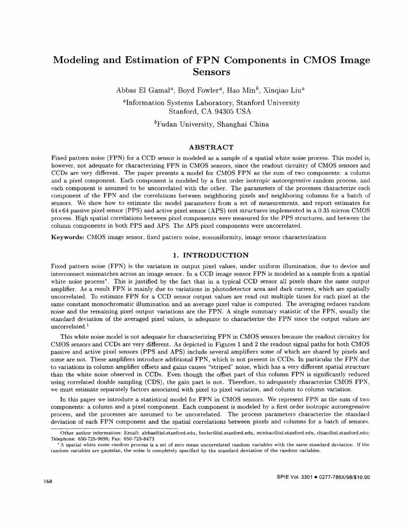
Figure 1. PPS signal path. Pixel FPN is caused by photodiode leakage, variations in photodiode area, channelcharge injection from Ml, and capacitive coupling from the overlap capacitance of Ml. Column FPN is causedby offset in the integrating amplifier(*), size variations in the integrating capacitor CF, channel charge injectionfrom M2(*), capacitive coupling from the overlap capacitance of M2(*), and threshold variations in M2(*). FPNcomponents that are reduced by CDS are marked with (*).
2. MODELING AND ESTIMATIONAssuming constant monochromatic illumination we model FPN as a two dimensional random process (random field)
where the F,3s are zero mean random variables representing the deviation of the output pixel values from thepixel value with no added random noise, and i and j are the row and column index respectively. To capture thestructure of FPN in a CMOS sensor we express F,3 as the sum of a column FPN component Y and a pixel FPNcomponent X,. Thus,
= Yj +where the Y3s and the X2,3s are zero mean random variables.
(1)
The goal of this work is to devise an FPN model to be used for measuring the quality for a batch of sensors orto simulate FPN, e.g. in a digital camera simulator. We would like the model to be simple, but accurate enough,
169
IT
ESET
vD0
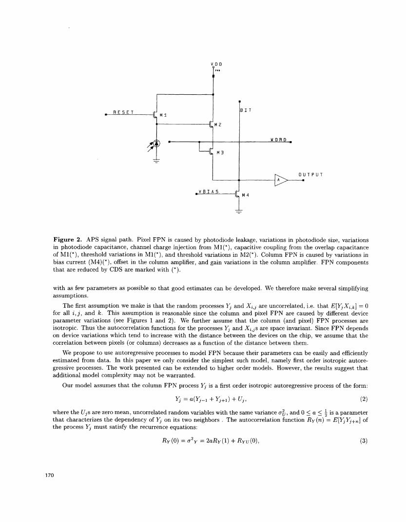
Figure 2. APS signal path. Pixel FPN is caused by photodiode leakage, variations in photodiode size, variationsin photodiode capacitance, channel charge injection from M1(*), capacitive coupling from the overlap capacitanceof M1(*), threshold variations in M1(*), and threshold variations in M2(*). Column FPN is caused by variations inbias current (M4)(*), offset in the column amplifier, and gain variations in the column amplifier. FPN componentsthat are reduced by CDS are marked with ().
with as few parameters as possible so that good estimates can be developed. We therefore make several simplifyingassumptions.
The first assumption we make is that the random processes } and Xj are uncorrelated, i.e. that E[YXj,k} =0for all i, j, and k. This assumption is reasonable since the column and pixel FPN are caused by different deviceparameter variations (see Figures 1 and 2) . We further assume that the column (and pixel) FPN processes areisotropic. Thus the autocorrelation functions for the processes Y and are space invariant. Since FPN dependson device variations which tend to increase with the distance between the devices on the chip, we assume that thecorrelation between pixels (or columns) decreases as a function of the distance between them.
We propose to use autoregressive processes to model FPN because their parameters can be easily and efficientlyestimated from data. In this paper we only consider the simplest such model, namely first order isotropic autore-gressive processes. The work presented can be extended to higher order models. However, the results suggest thatadditional model complexity may not be warranted.
Our model assumes that the column FPN process Yj is a first order isotropic autoregressive process of the form:
=a(i +}+i)+Uj, (2)
where the U3s are zero mean, uncorrelated random variables with the same variance a, and 0 < a < is a parameterthat characterizes the dependency of Y3 on its two neighbors . The autocorrelation function Ry (n) = E[Y+} ofthe process Y must satisfy the recurrence equations:
170
Ry(0) = cr2y 2aRy(1) + Ry(0), (3)
RESET M1IL
BIT
)M3
w 0 A 0
VBIAS
M4
T P U

Ry(O) = 2aRyu(1) + j, (4)
Ry(n) = a(Ry(n — 1) + Ry(n + 1)) + Ry(n), and (5)
Ryu(n) = a(Ryu(n — 1) + Ryu(n + 1)) (6)
for nf � 1.To estimate the model parameters a and a, we first estimate a2y and Ry(1) (using the estimators in equa-
tions 15, 17, and 19). We expressRy(1)py2y, (7)
where 0 py 1. Thus py can be directly estimated from the estimates of oy and Ry(1). It can be verified usingthe recurrence equations 3, 4, 5 and 6 that
pya=—--,and (8)
a = 4(1 - py) . (9)
Thus once 4 and py are estimated equations 8 and 9 can be used to estimate a and a.Our model assumes that the pixel FPN process X is a two dimensional first order isotropic autoregressive
process of the form:xi,j = b(X_1, + X+i, + + X,+1) + (10)
where the are zero mean uncorrelated random variables with the same variance 4, and 0 b is aparameter that characterizes the dependency of X2, on its four neighbors. The autocorrelation function R (in, n) =E{Xi,jXi+m,j+n]= Rx(ri, m) and the crosscorrelation function Rxv(m, n) = E{Xj,jVj+m,j+nJ R(n, m) satisfythe recurrence equations
R(0, 0) = cT2X = 4bR(0, 1) + R(0, 0), (11)
R(0, 0) = 4bRxv(0, 1) + cT2V, (12)
Rx(n,in) = b(R(n — 1,m) + R( + 1,rn) + Rx(n,m — 1) + Rx(n,m + 1)) + Rxv(n,m),and (13)
Rxv(n, m) = b(Rxv(n — 1,m) + Rxv(ri + 1,m) + Rxv(n, rn — 1) + m + 1)) (14)
for n, or mi � 1. To estimate the model parameters a and b we first estimate r and R(1, 0) = R(0, 1) usingthe estimators given in equations 15, 16, 18, and 20). Although it may be possible to solve the above recurrenceequations analytically we use the simple numerical method described in APPENDIX A. An advantage of this methodis that it can be readily used for more complex models.
Now to estimate the parameters of the model we measure pixel output values for a subsensor array of N x Mpixels under constant illumination. We repeat this measurement P times and average the values for each pixel toreduce the effect of random noise on the output values. We then compute the sample average output pixel value andsubtract it off the averaged values to obtain estimates of the F,3s. To simplify our analysis we assume that theseestimates are perfect, i.e. that we know the values of the F1,3s.
To estimate )' , , 4 , 4 , Ry(1), and R (0, 1) we use the following estimators:
(15)
X=F,—Y3, (16)
aM1}, (17)
N M— 1 —24= M(N-l' (18)' i=1 j=1
171

1M-1
Ry(1) = M — 1 T and (19)
N M—1 N—i M
Rx(O, 1) =2N(M — 1)
+ 2/f(N — 1)(20)
i=1 j=1 i=1 j=1
3. RESULTSIn this section we present the measured FPN results from our 64 x 64 pixel PPS and APS test structures2 fabricatedin a 0.35pm digital CMOS process. A summary of the main test structure characteristics are provided in Table 1.
- pPS APSTechnology 0.35 ,um, 4-layer metal
1-layer poly, nwell CMOS0.35 ,am, 4-layer metal1-layer poly, nwell CMOS
Number of Pixels 64 x 64 64 x 64Pixel Area 14um x 14im l4pm x 14imTransistors per pixel 1 3Fill Factor 37% 29%Photodetector nwell/psub diode nwell/psub diodePixel Interconnect Metall and Poly Metall and Poly
Table 1. Test Structure Characteristics in 0.35tm CMOS Technology
The setup used to measure FPN is described by Fowler et al. . It consists of a DC light source, a monochromator,an integrating sphere, and a calibrated photodiode. The measurements were performed under no illumination (dark)and at typical illumination using a monochromatic source, of wavelength A = 600nm. At the beginning of each arraymeasurement, all pixels are reset. The data is then read out after an integration time of 5Oms. The data from eachpixel consists of a signal sample and a reset sample. Each of the signal and the reset samples are amplified using avery low noise amplifier and then digitized using a 16 bit ADC. The amplifier is used to match the output swing ofthe sensor to the input range of the ADC. The array measurement is repeated P = 1024 times for each chip. Thesemeasurements are performed for eight PPS and eight APS chips with and without illumination. The chosen level ofillumination results in an output signal that is 70% of the maximum output signal swing.
The FPN results for the PPS and APS test structures with and without illumination are presented in Tables 2and 3, respectively. The tables present the estimated standard deviation and autocorrelation values averaged overthe eight chips and the derived process parameters based on the averaged estimates. All values are reported inequivalent input electrons. To find the input electron numbers we normalized the measured output voltage valuesusing the estimated gain numbers obtained from our QE measurements.3 These results translate into estimated darkFPN of 1 .7% and 0. 15% of full well capacity for PPS and APS respectively.
The results clearly show that CDS reduces FPN for both PPS and APS. It also shows that CDS is far less effectivewith illumination than without illumination. After CDS the PPS FPN is higher than that of the APS. The fact thatPPS column FPN is larger than that for APS is easily explained by the additional column charge integrating amplifierused in PPS. The higher PPS pixel FPN may be attributed to the charge injection from the overlap capacitancetransistor which is not canceled by CDS. It may also be due to the bias in the estimators.
The results also show that with illumination CDS increases FPN correlation between columns. This suggeststhat CDS removes the less spatially correlated FPN components, while leaving the more correlated ones unchanged.In particular since CDS eliminates column amplifier offset and bias current variations in APS, and column offsetvariation in PPS, the results suggest that these sources are rapidly varying from column to column. On the otherhand, variation in column amplifier gains, and the integrating amplifier capacitance CF in PPS are not removed byCDS and appear to be more spatially correlated.
The FPN correlation between pixels is high for PPS and low for APS. This suggests that variations in colunmamplifier offset, charge injection, and capacitive coupling, which dominate pixel FPN in PPS are highly correlated,while pixel area and dark current, which dominate pixel FPN in APS, vary rapidly from pixel to pixel.
172

______ PPSwithEstimated Statistics:
34332660456
10025512704561960011436130633217288
0.151866330.035558750
Table 2. Estimated statistics and parameters under uniform illumination (70% full well). The statistics areaveraged over all 8 chips. Note that , i, and T(oi) are the estimated standard deviations of theestimators.
CDS PPS without CD- APS with APS without CDS
(electrons2) 53519470 647555000 145550:;: (electrons2) 458044 17932700 7851Ry(1) (electrons2) 12255300 61853600 20862¶y(i) (electrons2) 1728000 1299050 4085
(electrons2) 4584010 4582680 597282(electrons2) 128423 144732 7133
Rx(0,1) (electrons2) 2217790 2211580 46763Rx (0,1) (electrons2) 83427 89529 3478
Estimated Paramteis:
0.11 0.05 0.09cr (electrons2) 36232900 557027000 87332b 0.19 0.19 0.044 (electrons2) 2321600 2320900 585761
PPS without DS APS with CDSEstimated Statisticj
(electrons2)
a;: (electrons2)
Ry(1) (electrons2)0Ry(1) (electrons2):j (electrons2):[ (electrons2)
R(0, 1) (electrons2)(0,1) (electrons2)
Estimated Paramters:
acr (electrons2)b
4 (electrons2)
656933045364596727119797151812108831229026891
0.0556948600.2419949
31732200016521500140110003122460
14610014329
1200679524
0.02
2965390000.2419199
8090032747742153744155
1660
3656
0.0570029
0.01
214
APS without CDS
45161168787159550170577144450105369
44288041255
0.18
2348660.037067090
Table 3. Estimated statistics and parameters under dark conditions. The statistics are averaged over all 8 chips.Note that au; (1) , and R(o,1) are the estimated standard deviations of the estimators.
173

Jo oitiiaie our nu.nleI with tjip iiieasured data we generated 61 xbl arnp1e FPN itti using the in H pa-taitieters iii IahIE's 2 and 3. 1 In nieasured and siniiilated FPN images fot and AI- wit Ii and vitInnit (I)ale 1iown in Ijgiiies 3 and 1. iespeutivelv. To display the 1P\ iniages we sealed eaeli non-( l) Ililage So liar tInniaximituin pixel value range is -hi;. Ladi CDS image was then sealed using the sano seam faetor as its lioti-( l)('oluuit(IjOlit .',ote that the •I illiages 1151 a seale laitor Ihat is eight tuuiies smiiallru than I hat lou I lie PPS uiageslhiise images (lImnonstrate that our model closely predicts FPN for PIS and APS.
101:1
20I I1t
30 40
Figure 3. iop h-ft —- nieasrued PPS FPN wit Hut CI)S. top right - Ifl(ilSIired PPS FPN wit hi (1)5. hot I 0111 left
siiuiiilatid lIS FIN without (1)5. and bottom right - simulated PPS FPN wit Ii (1)5.
10
20
30
40
50
01.)
60
5 p(\V
I-F
174

10
20
30
40
50
60
Figure 4. 101) 1(11 iii(asiire(1 A1 FPN without ('DS. to1) right measured AI FPN with (i). hot loin hitsiinuliit ed AP 1, j)\ without EDS. arid hottom right - simulated APS FPN with (1)5.
175
*1 -
_;.I-
SS s - fl..__ aS Sas. * . .S41.... S a saso . s

4. CONCLUSIONSWe described a new FPN model for PPS and APS CMOS image sensors. The model represents FPN as the sum oftwo components: a pixel and a column FPN component. Each component is modeled using a first order isotropic
. autoregressive process, and the processes are assumed to be uncorrelated. We presented a method for estimating theparameters of the processes and reported results that justify the added model complexity compared to the simplewhite noise model used in CCDs. The model appears to match the measured results well, as demonstrated by thesimilarity between the simulated and measured FPN images.
A number of issues remain to be investigated. The estimators we used are biased and may have unacceptablylarge variances, which may have caused several inaccuracies in our results. More data and more analysis is needed toverify the accuracy of the estimators. It may in fact be necessary to find better estimators. The 64x64 pixel sensorswe measured are too small to adequately represent FPN in real sensors. In particular for a large sensor there may bea need to model the effect of systematic device variation across the sensor. Finally, a weakness of our model is thatit does not separately model gain and offset FPN components. Fowler et al.3 report preliminary gain FPN results.However, no method for estimating gain FPN correlation was provided. To use our model for characterizing gainFPN we need to fit the model to several levels of illumination resulting in a very large amount of collected data anda large number of parameters to be estimated. A model with less parameters needs to be developed.
ACKNOWLEDGEMENTSWe wish to thank HP, Intel, and the Center for Integrated Systems (CIS) for their support of this project. In additionwe wish to thank Hui Tian for performing the experiments, and Brian Wandell for his comments and suggestions.
APPENDIX A. PIXEL PARAMETER ESTIMATIONTo estimate the model parameters b and 4 we consider an array with N = M = 21 + 1 and with zero boundaryconditions and arrange equation 10 in vector notation using a raster scan pixel format to obtain
V=AX, (21)
where V = [V1,1 Vi,2 . . . ViM V2,1 . ... VN,M}T, and X = [X1,1 Xi,2 . . . X1,M X2,1 . . . XN,M}T. Using this notationit can be verified that the covariance matrix of X is
= cA_lA_T. (22)
The finite image size and zero boundary conditions result in Ex which is not isotropic. For example, cT.. is not aconstant and depends on the pixel distance from the edge of the array. In our isotropic model ax1, is a constant.The error caused by this model truncation can be minimized by choosing a large enough array size and using thevalues for the pixel at the center of the array. Let A_1A_T(212 + 21 + 1, 212 + 21 + 1) be the center entry of thematrix A' A_T we estimate b by finding a value 0 b < - such that equation 23 is minimized.
R(O, 1) A_1A_T(212 + 21 + 1, 212 + 21 + 2)(23)- A_1A_T(212+21+1,212+21+1)
We then use b to compute A. The estimate of 4 is then found by
=— — . (24)V (Ay(A)T(2l2 + 21 + 1,212 + 21 + 1)
For the results reported in the paper we used values for I in the range of 7 to 13.
176

REFERENCES1. J. Janesick et al., "Charge-coupled-device response to electron beam energies of less than 1 keV up to 20 keV,"
Optical Engineering 26, pp. 686—91, August 1987.2. D. Yang, B. Fowler, A. El Gamal, H. Mm, M. Beiley, and K. Cham, "Test Structures for Characterization and
Comparative Analysis of CMOS Image Sensors," in Proceedings of SPIE, (Berlin, Germany), October 1996.3. B. Fowler, A. El Gamal, and D. Yang, "A Method for Estimating Quantum Efficiency for CMOS Image Sensors,"
in Proceedings of SPIE, (Sari Jose, CA), January 1998.
177


![arXiv:1912.05027v3 [cs.CV] 17 Jun 2020 · COCO AP (%) MnasNet-A1 (SSD) NAS-FPN (RetinaNet) MobileNetV2-FPN (RetinaNet) MobileNetV3 (SSD) SpineNet-Mobile (RetinaNet) 49XS 49S 49 #FLOPsN](https://static.fdocuments.us/doc/165x107/5f76deaaf648490502022d7b/arxiv191205027v3-cscv-17-jun-2020-coco-ap-mnasnet-a1-ssd-nas-fpn-retinanet.jpg)


![Auto-FPN: Automatic Network Architecture Adaptation for ...openaccess.thecvf.com/content_ICCV_2019/papers/Xu_Auto-FPN_Au… · FPN) [30]. To build an efficient yet accurate detector,](https://static.fdocuments.us/doc/165x107/5eadb209a076ec1fc6264bdd/auto-fpn-automatic-network-architecture-adaptation-for-fpn-30-to-build.jpg)