Modal analysis of transport processes in SPRITE detectors · This process shows the ... its spatial...
11
Modal analysis of transport processes in SPRITE detectors Frank J. Effenberger and Glenn D. Boreman Carrier transport in signal-processing-in-the-element 1SPRITE2 detectors is an important phenomenon because it determines properties such as the responsivity and the modulation transfer function 1MTF2. The previous literature has presented approximate solutions to the transport problem that neglect boundary effects, which have long been thought to play a major role in SPRITE behavior. We present a new solution to the problem through the use of modal analysis. This method intrinsically includes boundary conditions and thus is more complete than the previous analysis. Furthermore we use this solution to derive expressions for the MTF. The effects of the boundary conditions on the MTF are studied to determine their optimum values. Key words: SPRITE, IR detectors, charge transport, MTF. 1. Introduction Signal-processing-in-the-element 1SPRITE2 detec- tors 1,2 provide improvement in the signal-to-noise ratio over simpler photoconductive detectors through the use of a virtual time-delay-and-integration pro- cess internal to the detector element. The drift transport of carriers through the detector is the mechanism that makes this possible. Other trans- port mechanisms, such as recombination and diffu- sion, tend to degrade detector performance. Under- standing the interplay of these effects with the electrical boundary conditions would permit better understanding of existing devices and provide further guidance in the design and manufacture of new SPRITE detectors. In previous analyses, 3–5 a one-dimensional Green’s function was taken as the solution to the transport equation. This solution, which describes the charge distribution in an infinite one-dimensional solid result- ing from a point source, is used as the basis of calculations to compute the transfer of a scanned incident-radiation distribution on the SPRITE detec- tor bar into the output as seen at the readout terminals. This theory does not show complete agreement with the measurements of real devices. 6 The definition of the Green’s function implicit to the analysis omits key physical phenomena in its development. The steps subsequent to the generation of the Green’s function are straightforward applications of linear-systems theory and are generally valid for this type of analysis. We have therefore used a different method, modal analysis, to solve the charge-transport equation and developed an equivalent analysis of the transfer function of SPRITE detectors. The method of modal analysis is more capable and requires fewer assumptions than the previous Green’s- function method. The first improvement is that modal analysis is multidimensional, whereas the Green’s-function method is one dimensional. Although the single-dimensional approach may suf- fice for long, slender detector bars, most practical devices have aspect ratios that are only near 10. This fact requires consideration of the transverse dimensions. The second improvement is that the boundary conditions are included in modal analysis. The Green’s function method has no boundary conditions because of the implicit assumption of an infinite solid. The boundary conditions are important because 112 the readout is usually placed at one end of the detector and 122 most contacts made to HgCdTe show partial blocking behavior, 7 which leads to carrier accumulation at the contacts. Thus the inclusion of boundary conditions has a considerable effect. Our modal solution is found by use of the method of separation of variables on the transport equation The authors are with the Center for Research and Education in Optics and Lasers, Department of Electrical and Computer Engi- neering, University of Central Florida, Orlando, Florida 32816. Received 5 October 1994; revised manuscript received 31 Janu- ary 1995. 0003-6935@95@224651-11$06.00@0. r 1995 Optical Society of America. 1 August 1995 @ Vol. 34, No. 22 @ APPLIED OPTICS 4651
Transcript of Modal analysis of transport processes in SPRITE detectors · This process shows the ... its spatial...
Modal analysis of transportprocesses in SPRITE detectors
Frank J. Effenberger and Glenn D. Boreman
Carrier transport in signal-processing-in-the-element 1SPRITE2 detectors is an important phenomenonbecause it determines properties such as the responsivity and the modulation transfer function1MTF2. The previous literature has presented approximate solutions to the transport problem thatneglect boundary effects, which have long been thought to play a major role in SPRITE behavior. Wepresent a new solution to the problem through the use of modal analysis. This method intrinsicallyincludes boundary conditions and thus is more complete than the previous analysis. Furthermore weuse this solution to derive expressions for the MTF. The effects of the boundary conditions on the MTFare studied to determine their optimum values.Key words: SPRITE, IR detectors, charge transport, MTF.
1. Introduction
Signal-processing-in-the-element 1SPRITE2 detec-tors1,2 provide improvement in the signal-to-noiseratio over simpler photoconductive detectors throughthe use of a virtual time-delay-and-integration pro-cess internal to the detector element. The drifttransport of carriers through the detector is themechanism that makes this possible. Other trans-port mechanisms, such as recombination and diffu-sion, tend to degrade detector performance. Under-standing the interplay of these effects with theelectrical boundary conditions would permit betterunderstanding of existing devices and provide furtherguidance in the design and manufacture of newSPRITE detectors.In previous analyses,3–5 a one-dimensional Green’s
function was taken as the solution to the transportequation. This solution, which describes the chargedistribution in an infinite one-dimensional solid result-ing from a point source, is used as the basis ofcalculations to compute the transfer of a scannedincident-radiation distribution on the SPRITE detec-tor bar into the output as seen at the readoutterminals.
The authors are with the Center for Research and Education inOptics and Lasers, Department of Electrical and Computer Engi-neering, University of Central Florida, Orlando, Florida 32816.Received 5 October 1994; revised manuscript received 31 Janu-
ary 1995.0003-6935@95@224651-11$06.00@0.
r 1995 Optical Society of America.
This theory does not show complete agreement withthe measurements of real devices.6 The definition ofthe Green’s function implicit to the analysis omits keyphysical phenomena in its development. The stepssubsequent to the generation of the Green’s functionare straightforward applications of linear-systemstheory and are generally valid for this type of analysis.We have therefore used a different method, modalanalysis, to solve the charge-transport equation anddeveloped an equivalent analysis of the transferfunction of SPRITE detectors.The method of modal analysis is more capable and
requires fewer assumptions than the previousGreen’s-function method. The first improvement is thatmodal analysis is multidimensional, whereas theGreen’s-function method is one dimensional.Although the single-dimensional approach may suf-fice for long, slender detector bars, most practicaldevices have aspect ratios that are only near 10.This fact requires consideration of the transversedimensions.The second improvement is that the boundary
conditions are included in modal analysis. TheGreen’s function method has no boundary conditionsbecause of the implicit assumption of an infinite solid.The boundary conditions are important because 112the readout is usually placed at one end of thedetector and 122 most contacts made to HgCdTe showpartial blocking behavior,7 which leads to carrieraccumulation at the contacts. Thus the inclusion ofboundary conditions has a considerable effect.Our modal solution is found by use of the method of
separation of variables on the transport equation
1 August 1995 @ Vol. 34, No. 22 @ APPLIED OPTICS 4651

followed by determination of the eigenmodes of theseparated equations.8 This process is shown to in-clude the pertinent features of the system while stillproducing closed-form solutions. In Section 2 amorecomplete definition of the SPRITE transport problemis given. Then the modal solutions are developedand described. After this, we use the modal solu-tions to compute the impulse response, and then thisis converted into the MTF of the detector. Finally,some conclusions are drawn about the general behav-ior of the MTF and the modal parameters.
2. Transport Problem
SPRITE detectors are complex devices with manyfeatures that are not easily analyzed. Among theseare details of the readout geometry, the electricalproperties of the passivated surfaces, and the current-voltage characteristics of the electrical contacts.Although a complete model of all these factors re-quires a numerical solution,9 simplifications can bemade to yield a self-consistent model that can besolved analytically and yet still contains the mainfeatures. In this section such amathematical descrip-tion of the SPRITE transport problem is given.A diagram of our idealized detector is shown in Fig.
1. The detector is a rectangular solid with length,width, and depth denoted 2l, 2w, and 2d, respectively.The device has contacts on the two ends that arenominally ohmic. The top, bottom, and side surfacesare all passivated insulating boundaries. A sensinglead is placed on the bar near the output end. Thislead measures the voltage across the readout zone ofthe detector and is connected to a high-impedanceamplifier.Operation of this detector hinges on the ambipolar
drift of photon-generated minority carriers. MostHgCdTe-based SPRITE’s are made of an n-typesemiconductor, and thus the minority holes carry thesignal of interest. If the light source is scannedalong the length of the bar, and the carriers driftalong with it at the same speed, the detected signal isamplified and reinforced. This process shows thesame character and advantages as a time-delay-and-integration system but without the necessity of sepa-rate delay-line electronics. When the intensifiedcharge reaches the end of the detector, it causes thevoltage on the sensing lead to change, thus generat-ing a signal.
Fig. 1. SPRITE detector model geometry and coordinate system.
4652 APPLIED OPTICS @ Vol. 34, No. 22 @ 1 August 1995
The basis for the model is the transport equation:
≠r
≠t5 D=2r 2 µ= · 1rEzk̂2 2
r
t1 G. 112
This equation assumes that the carriers in the devicecan be described by a volumetric density r, and thematerial can be described by a diffusivity D, mobilityµ, and minority carrier lifetime t and that there is aspatially invariant generation rateG. These assump-tions ignore the particulate nature of the charge andthe resultant inherent randomness of their genera-tion, motion, and recombination. Thus it can be saidthat this equation deals with the average values forall the quantities concerned and is deterministic.This equation also neglects the momentum of thecarriers, assuming that the mean free path in thematerial is short compared with any other dimensionof the device. This last assumption is valid inSPRITE structures because the devices are long andthe electric fields are low.The major assumption implicit in Eq. 112 is that the
product of the electric field and mobility, which equalsthe carrier-drift velocity, is assumed to be constant.This implies that the device is designed and operatedin a manner that generates this condition at steadystate. For simple rectangular detectors, integrationof the background radiation causes this product tovary slowly over the length of the bar, with a totalchange of ,25%.9 By tapering the detector bar, thisnonuniformity can be reduced to insure a constantdrift velocity. Also Eq. 112 assumes that the photogen-erated carriers themselves do not generate significantspace-charge fields. This is true for SPRITE’s be-cause the bias current and its associated electric biasfield are much stronger than the detected imagesignal and its field.The boundaries of the bar, as mentioned above, are
nominally either ohmic or insulating. Observationson actual devices,10 however, indicate behavior thatdiffers from ideal conduction or insulation. Althoughreal surfaces are difficult to describe fully, we take thefirst level of complexity, which is to ascribe a surfacevelocity Vs to the passivated surfaces and to thecontacts.11 The surface velocity relates the carrierdensity at the surface to the carrier flux, leavingthrough that surface according to
F · n̂ 5 Vsr. 122
Carrier flux F is a vector quantity, and the normalunit vector n̂ is defined to be pointing out of thedetector volume. The flux is caused by diffusion anddrift in our model and thus can be written as
F 5 2D=r 1 µEZr. 132
If we apply this definition to the six surfaces of thedetector bar, using the coordinate system shown inFig. 1, we can produce three pairs of equations that

describe the boundary conditions:
D≠r
≠x5 Vxr 0 x5 2w, D
≠r
≠x5 2Vxr 0 x51w, 14a2
D≠r
≠y5 Vyr 0 y52d, D
≠r
≠y5 2Vyr 0 y51d, 14b2
D≠r
≠z5 1µE1Vz2r 0 z52l, D
≠r
≠z5 1µE2Vz2r 0 z5l. 14c2
Note that Eqs. 142 assume that the bias contacts areformed exclusively on the endfaces of the detector bar,neglecting any geometrical details of the actual con-tacts. Real contacts are typically formed partly onthe endface and partly on the top face. Such acontact dictates boundary-condition equations thatcannot be easily incorporated into our solution. Ouridealized bias-contact geometry is a close approxima-tion to reality when the top contact length is smallcompared with the thickness of the detector bar.Also, Eqs. 142 ignore any effects of the sensing contact.This is a good approximation if this contact is madesmall and if the amplifier used has a sufficiently highimpedance.The transport equation and the three pairs of
boundary conditions fully describe our SPRITE-transport model. This model does not ignore anyfeature of the detector that is vital to its operation.As shown in Section 3, it also has a closed-formsolution. These factors result in amodel that is morerealistic than other models described previously.
3. Modal Solutions
The first step in the solution of Eq. 112 is to perform atransformation of the dependent variable to make theequation homogeneous. This discards that part ofthe charge distribution, equal to Gt, caused by back-ground illumination. As mentioned above, the back-ground charge influences detector performance in adeleterious way by making the drift velocity vary overthe length; however, in all the following calculations itis assumed that steps have been taken to correct forthis problem and the effect is ignored. Regardless ofits spatial distribution, the background charge isconstant in time. It therefore represents an unchang-ing offset on the signal and is of no interest as far assignal transfer is concerned. The transformation is
r 5 r8 1 Gt. 152
Next, we scale all the independent variables to thenatural metrics of the problem, namely, the detectordimensions for the spatial coordinates and the carrierlifetime for the time:
x8 5x
w, y8 5
y
d, z8 5
z
l, t8 5
t
t. 162
The scaled coordinates are all denoted by a prime,which results in the following equation 1with vector
operators expanded2:
≠r8
≠t85 tD1 ≠2r8
w2≠x821
≠2r8
d2≠y821
≠2r8
l2≠z822 2µEzt
l
≠r8
≠z82 r8.
172
Next we employ the technique of separation ofvariables, which assumes that the solution for r8 canbe written as
r8 5 T1t82X1x82Y1 y82Z1z82exp1µEzl
2Dz82 . 182
This generates one time equation and three spaceequations:
≠T
≠t81 k2T 5 0, 19a2
≠2X
≠x821 kx2X 5 0, 19b2
≠2Y
≠y821 ky2Y 5 0, 19c2
≠2Z
≠z821 kz2Z 5 0. 19d2
We have defined the time separation constant to be k2and the x, y, and z separation constants to be kx2, ky2,and kz2, respectively. These constants are related bythe simple equation
k2 5 Nsxkx2 1 Nsyky2 1 Nszkzr2 1 Ndz2Nsz 1 1. 1102
We have defined the dimensionless combinations ofconstants in Eq. 1102 as follows:
Nsx 5Dt
w2, Nsy 5
Dt
d2, Nsz 5
Dt
l2, Ndz 5
µEzl
2D. 1112
The constants denoted Nsx, Nsy, Nsz are the ratios ofthe carrier recombination lifetime to the carrierspatial-relaxation lifetimes, and they depend on thephysical dimensions of the detector, the diffusivity,and the carrier lifetime of the material. By thespatial-relaxation lifetime, we refer to the characteris-tic time for localized disturbances in the carrierdistribution to spread because of diffusion. Themagnitude of Nsx, Nsy, Nsz determines whether diffu-sion or recombination is the dominant process ofcarrier-distribution relaxation. The constant Ndz re-lates the lifetime of the charge distributions to thetransit time of carriers in the device. It determinesthe degree of diffusional spreading that occurs duringthe time the carriers drift and accumulate in thedetector.We note that the time equation is of first order and
has the solution
T1t82 5 exp12k2t82. 1122
1 August 1995 @ Vol. 34, No. 22 @ APPLIED OPTICS 4653

The x, y, and z equations are second order and havegeneral solutions:
X1x82 5 cxp cos1kxpx8 1 pp
22 , 113a2
Y1 y82 5 cyq cos1kyqy8 1 qp
22 , 113b2
Z1z82 5 czr cos1kzrz8 1 rp
22 , 113c2
where p, q, and r are the serial numbers for the x, y,and z solutions, respectively.Now that the general solutions have been written,
the boundary conditions can be applied. Because thevariables have been scaled and separated, Eqs. 142must be modified, producing new equations:
≠X
≠x85 NbxX 0 x8521,
≠X
≠x85 2NbxX 0 x8511, 114a2
≠Y
≠y85 NbyY 0 y8521,
≠Y
≠y85 2NbyY 0 y8511, 114b2
≠Z
≠z85 NbzZ 0 z8521,
≠Z
≠z85 2NbzZ 0 z8511, 114c2
where we define three new dimensionless boundarynumbers:
Nbx 5Vxw
D, Nby 5
Vyd
D, Nbz 5
Vzl
D. 1152
These constants describe the ratio of the boundaryvelocities with the diffusion velocity, that is, thevelocity at which diffusion spreads disturbances acrossthe device. It provides a comparison of the speed ofsurface recomination with the speed of diffusion.By substituting the general solutions into these
equations, we can find the allowed values of theseparation constants, thus completing the solution.This results in the following transcendental relations:
kxp 5 Nbx cot1kxp 1 pp
22 , 116a2
kyq 5 Nby cot1kyq 1 qp
22 , 116b2
kzr 5 Nbz cot1kzr 1 rp
22 . 116c2
Figure 2 is a graph of the first few roots of any of Eqs.1162 as a function of the boundary parameter, Nbx, Nby,or Nbz. A series of roots results from this type ofequation because the mode indices, p, q, or r, canassume all positive integer values. For small orlarge values of the boundary parameter, the curvestend toward limiting asymptotes.
4654 APPLIED OPTICS @ Vol. 34, No. 22 @ 1 August 1995
So far we have named seven independent dimen-sionless numbers that describe the model of theSPRITE detector. We now show that this is thecorrect number of constants needed to describe theproblem as given. The model developed in Section 2has nine independent parameters: length, width,and depth of the detector; surface velocities of theends, sides, and faces; diffusivity; lifetime; and driftvelocity. With this problem two units of measure areused, length and time. The p theorem12 states thatthe number of independent dimensionless constantsneeded to describe a problem is equal to the number ofmeasured parameters less the number of units ofmeasure. Thus for our problem this states thatseven numbers are necessary. Because the sevennumbers defined here are independent from oneanother, they must form a sufficient, complete set ofnumbers completely describing the problem. To pro-vide a feeling for the usual ranges for these numbers,typical values for these numbers have been computedwith the data in Refs. 2 and 7 and are shown inTable 1.Although our set of dimensionless numbers are
complete, they do not represent the only set of num-bers that could be formulated that have this property.What makes them particularly useful for our analysisis that they appear so naturally and explicitly in thedifferential equations and their solutions. This botheases the expression of the solutions and providesinsight into the actual influence of the device param-eters on device performance. This can be seen in thecase of the boundary numbers.Intuitively the best detector will have no recombina-
tion on the sides and faces and have ohmic contacts atthe ends. Any realistic fabrication process cannot
Fig. 2. Solutions to the modal wave numbers versus boundarynumber. Note how the solutions approach the asymptotes.
Table 1. Typical Values of the Detector Numbers for SPRITE Detectors
Parameter Value
Ndz 75Nbx 15 3 1023
Nby 2.5 3 1023
Nbz 3.75Nsx 1.0Nsy 36Nsz 6.4 3 1023

achieve such surfaces, however, and thus the questionis raised as to how good the surfaces need to be. Thisquestion can be answered through use of the bound-ary numbers. The asymptotic behavior shown inFig. 2 demonstrates that, for sufficiently large orsmall values of the boundary number, no furtherchange in the modal wave numbers occurs. Becausethese wave numbers are the only way in which theboundary conditions can affect the final solution, wecan justifiably say that, for practical purposes, aboundary number of less than 1@100 is insulating andthat a boundary number greater than 100 is ohmic.The equations above describe the complete family
of solutions to the transport problem. Their applica-tion requires finding the roots of Eqs. 1132, which aretranscendental. This makes their use difficult. Itis thus interesting to look at the idealized case wherethe contacts are purely ohmic 1Nbz 5 `2 and the insu-lating surfaces are truly blocking 1Nbx 5 Nby 5 02.This results in a simple set of solutions for kxp, kyq, kzr.
kxp 5 pp
2, kyq 5 q
p
2, kzr 5 1r 1 12
p
2. 1172
These ideal boundary conditions enable us to writethe full solution for r8 as
r81x8, y8, z8, t82 5 op,q,r
cpqr exp12kpqr2t82cos3pp
21x8 1 124
3 cos3q p
21 y8 1 124sin3r p
21z8 1 124 ,
118a2
kpqr2 5p2
41Nsxp2 1 Nsyq2 1 Nszr22
1 NszNdz2 1 1. 118b2
In Section 4 we show that the assumption of theseboundary conditions greatly simplifies the computa-tional form of the transfer function.
4. Modulation Transfer Function
Now that the behavior of the individual modes of theSPRITE structure have been determined, we canderive the modulation transfer function 1MTF2 of thedetector. The MTF provides the most convenientexpression of signal fidelity performance for imagingsystems. Thus it is useful to compute the MTF fromthe physical parameters of the device. In this sec-tion we derive a general form for the MTF and special
cases that result in simplification. Several familiesof MTF curves are computed and compared to detecttrends in the general character of the MTF as afunction of detector parameters.We first define the input presented to the detector.
Because the SPRITE is used as a one-dimensionaldetector, we use a one-dimensional d function that canbe scanned across the detector aperture:
qi1z8, t82 5 d1z8 2 z082, 1192
where the scanned location z08 is given by
z08 5 n8t8 5 t8@n8. 1202
The constants in Eq. 1202, n8 and n8, represent thenormalized scanning velocity and its inverse, respec-tively. Because the scan is typically matched to thedrift velocity, we can write
n8 5t
lµEz 5 21
µEzl
2D 21Dt
l2 2 5 2NdzNsz. 1212
Although this input is one-dimensional, the three-dimensional nature of our solution does not necessar-ily vanish. When decomposed, this input produces athree-dimensional series of modes, each with its owndecay-time constant. We now decompose this inputinto the modes of the structure:
qi 5 op,q,r
cpqrXp1x82Yq1 y82Zr1z82exp1Ndzz82. 1222
Because the circular-function portion of the eigenfunc-tions are orthogonal, we can solve for the amplitudesof the individual modes arising from the input at anyparticular point z08, giving
cpqr 5
eee dx8dy8dz8Xp1x82Yq1 y82Zr1z82exp12Ndzz82d1z8 2 z082
eee dx8dydz8Xp21x82Yq
21 y82Zr21z82
, 1232
Performing the indicated integrations over the entiredomain of the detector, 21 , x8 , 1, 21 , y8 , 1,21 , z8 , 1, we obtain
cpqr 50sinc1kxp2 0
31 1 0sinc12kxp2 0 4
0sinc1kyq2 0
31 1 0sinc12kyq2 0 4
3
exp12Ndzz082cos1kzrz08 1 rp
2231 1 0sinc12kzr2 0 4
1242
if p and q are even. If p or q is odd, cpqr 5 0. Thesemode coefficients represent the amplitude of each
1 August 1995 @ Vol. 34, No. 22 @ APPLIED OPTICS 4655
mode that results from the d-function input at thespecified z8 coordinate z08. These amplitudes thenfully specify the carrier distribution inside the detec-tor for all time after the input. Thus these modecoefficients essentially translate the given input intoa charge distribution inside the detector.We next evaluate the output voltage resulting from
a given set of modes as they decay over time. In theSPRITE the measured output voltage is proportionalto the charge in the readout region. The outputresulting from charge generation located at z08 is thusproportional to the charge in the readout volume Qgiven by
Q1t8, z082 5 opqr
cpqru1t8 2 n8z082
3 exp32kpqr21t8 2 n8z824bpqr, 1252
where bpqr are the mode output weighting factors,given by the integration of the eigenfunctions over thescaled readout volume:
bpqr 5 e21
1
dx8 e21
1
dy8 e12lr8
1
dz8Xp1x82Yq1 y82Zr1z82
3 exp12Ndzz82. 1262
Evaluation of these integrals give the result
4656 A
bpqr 50sinc1kxp2 0 0sinc1kyq2 0
Ndz2 1 kzr2
exp1Ndz2 531 2 cos1kzrlr8243Ndz cos1kzr 1 r
p
22 1 kzr sin1kzr 1 rp
2241 sin1kzrlr823Ndz sin1kzr 1 r
p
22 1 kzr cos1kzr 1 rp
224 6 , 1272
if p and q are even. If p or q is odd, bpqr 5 0.The total scanned impulse response U as a function
of time is the point impulse response Q integratedover the entire scan, that is, over the entire detector.
Thus
U1t82 5 e21
1
dz08Q1t8, z082. 1282
PPLIED OPTICS @ Vol. 34, No. 22 @ 1 August 1995
Because we are ultimately interested in obtaining thetransform of the scanned function U, we choose totake the transform now, yielding
U1v82 5 e21
1
dz08Q1v, z082. 1292
We thus need the time-domain Fourier transform ofQ1t, z2, which can be found to be
Q1v8, z082 5 F 5Q1t8, z0826
5 opqr
cpqrbpqrexp12 jn8v8z082
kpqr2 1 jv8
. 1302
Substituting this into the integral for the total output,we can write
U1v82 5 e21
1
dz08 opqr
cpqr8exp12Ndz 2 jn8v82z08
kpqr2 1 jv8
3 cos1kzrz08 1 rp
22 , 1312
where we have defined a new set of constants cpqr8,which contains all the factors independent of theposition of the input z08. We do this because wemust integrate over this variable, and these factors
will not play a role in this integration. These con-stants are defined as
cpqr8 5 bpqr0sinc1kxp2 00sinc1kyq2 0
31 1 0sinc12kxp2 0 431 1 0sinc12kyq2 0 431 1 0sinc12kzr2 0 4, 1322
If we now integrate Eq. 1312 term by term, we arrive atthe final result:
U1v82 5 opqr
cpqr853exp12Ndz 2 jn8v8z82 1 1212rexp1Ndz1 jn8v8z824
3 3kzr sin1kzr 1 rp
22 2 1Ndz 1 jn8v82cos1kzr 1 rp
22463kpqr2 1 jv8431Ndz 1 jn8v822 1 kzr24
. 1332
This is an expression for the Fourier transform ofthe impulse response of a SPRITE detector asdescribed by our model. The MTF is simplythe normalized magnitude of this function, writ-

ten as
MTF1 fz2 5 0U12pln8fz2
U102 0 , 1342
where fz is the spatial frequency measured in cyclesper unit length 1i.e., cycles@mm2. Note that in thefigures cited in Section 5, the frequency is given interms of cycles per detector length.This transfer function is admittedly complex, but
one can observe a few general facts about its structure.It is an infinite sum of terms, each composed of threefactors. The first factor cpqr8 is a modal weight thatdepends on the particular parameters of the structure.These weights decrease in size with increasing modalserial numbers, which ensures a bounded response.The second, the denominator in Eq. 1332, is a combina-tion of complex poles that describes the main low-passfiltering of the device. The characteristic frequency
of these poles increaseswith themodal serial numbers.The third, which is the factor of Eq. 1332 enclosed inbraces, is a phasing factor that describes the coher-ence of the signal integration over the length of thedevice, which depends on the scanning velocity.These three properties all contribute to the properfunctioning of the SPRITE detector.If the boundary parameters are either very small
1less than 0.012 or very large 1greater than 1002, asmentioned above, considerable simplification can re-sult. We demonstrate this by two steps: first, bymaking the walls of the device perfect insulators and,second, by adding the constraint that the contacts areperfectly ohmic.When the walls are perfect insulators, their recom-
bination velocity is zero; thus the x and y boundarynumbers are also zero. This greatly simplifies themodal weights, and all elements where p or q isnonzero vanish. The remaining modal weights canbe written as
cpqr8 5exp1Ndz2
1Ndz2 1 kzr2234 1 4 0sinc12kzr2 0 4 5
31 2 cos1kzrlr8243Ndz cos1kzr 1 rp
22 1 kzr sin1kzr 1 rp
2241 sin1kzrlr823Ndz sin1kzr 1 r
p
22 1 kzr cos1kzr 1 rp
224 6 1352
if p 5 q 5 0; cpqr8 5 0 otherwise.This simplification collapses the three-dimensional
sum of Eq. 1332 into a one-dimensional sum over theinteger values of r alone and yields considerablesavings in numerical effort in the calculation of theMTF.When the contacts are made completely ohmic, in
addition, all three factors in the terms of the transferfunction are affected. The modal weights can thenbe written
c00r8 51212rexp1Ndz2
43Ndz2 1 1p22
2
1r 1 1224
3 551 2 cos31p221r 1 12lr8461p221r 1 12
1 Ndz sin31p221r1 12lr84 6 , 1362
and the total output spectrum can be written
U1v82 5 orc00r8
31212rexp321Ndz 1 jn8v824 1 exp1Ndz 1 jn8v824p
21r 1 12
5Nsz3Ndz2 1 1p22
2
1r 1 1224 1 1 1 jv631Ndz 1 jn8v822 1 1p222
1r 1 1224. 1372
At this point the solution does not involve transcenden-tal roots which enables us to write the solution in aclosed form.The finite extent of the readout area was intrinsic
to the development of the results here. To removethe filtering effects caused by the spatial convolutionof the readout with the image,13 we can take the limitof the result as the readout length approaches zero.This changes only the modal weights, generating
c00r8 5
1212rexp1Ndz2Ndz1p221r 1 12lr8
43Ndz2 1 1p22
2
1r 1 1224. 1382
These modal weights can then be substituted backinto the transfer function 3Eq. 13724.Because the MTF is expressed as an infinite sum,
we can compute only an approximation of its value.
This inaccuracy is in the computation only and can bearbitrarily reduced through the inclusion of more
1 August 1995 @ Vol. 34, No. 22 @ APPLIED OPTICS 4657

terms in the series and by the use of higher-precisioncomputation. It is important to determine the num-ber of terms necessary to achieve a given level ofaccuracy. The x and y summations are driven toconverge by the sinc2 functional dependence of themodal weights. Our studies show that, for the typi-cal values listed above, the x and y series converge to0.1% in very few terms 1of the order of 102. Thez-series behavior can be understood best by observingthe simplified case of perfect boundary conditions.The sum, whose terms alternate sign, is driven toconvergence by the factors Ndz
2 1 1p@2221r 1 122 in thedenominator of each term. Thus it is necessary tocontinue the sum until the z serial number is muchlarger than the drift numberNdz. We find that of theorder of 10,000 terms are necessary to achieve 0.1%accuracy.
5. Results and Discussion
A computer program was developed to evaluate Eq.1332 for a given set of parameters and frequencies.We used a Microsoft FORTRAN compiler running on a486DX2@66-based desktop personal computer. Double-precision computations were used to preserve theaccuracy of the sum because the sum’s oscillatorybehavior tends to amplify round-off errors. MTFcurves could be generated in less than 10 min withthis system, thus proving the tractability of thisnumerical approach.Figure 3 shows the MTF for a detector with the
typical values given in Table 1 along with the curve ascomputed with the Green’s-function analysis for thesame parameters in Refs. 3–5. Both show similarlow-pass behavior, but the modal analysis predicts alower roll-off frequency than the Green’s-functionanalysis. This would put the modal analysis inbetter agreement with the measured responses of realSPRITE devices.Because the modal analysis includes the boundary
conditions in the solution of the problem, we canstudy their effects. In Fig. 4 we have plotted MTF’sof detectors with different insulating surface-recombi-nation rates. The velocity was varied from 1@100 to100 times the nominal value in Table 1. The resul-tant curves show little or no effect on the MTF until
Fig. 3. Computed MTF’s for the Green’s-function method and theeigenmode method.
4658 APPLIED OPTICS @ Vol. 34, No. 22 @ 1 August 1995
the surface recombination becomes fairly strong.It is interesting that the less insulating the sidesbecome, the wider the MTF’s become. This can beunderstood by considering the surface recombinationas a modal-damping effect. Higher recombinationmakes the higher transverse modes of the devicedissipate faster, and this makes the overall responsefaster. However, dissipation of the signal chargealso reduces the absolute signal levels. This can beseen in Fig. 5, which shows the signal transferfunction 1SiTF2 for the same conditions as in Fig. 4.The SiTF shown is obtained by normalizing all thecurves by the zero-frequency response of the typicalparameter response. From this figure it is clear thatthe broadening of the MTF comes at the cost of areduction in the level of the signal at all frequencies.Figure 6 shows the zero-frequency SiTF plotted as afunction of the insulating boundary condition. Thesignal level is normalized to one at the nominal valueof insulating boundary parameters, and it drops asthese parameters are made more conductive. Wecan thus conclude that it is best to reduce the surfacerecombination, but only because it improves the sig-nal efficiency of the detector and not because of MTFconsiderations.The effect of the width of the SPRITE detector can
be studied directly with modal analysis. It was
Fig. 4. MTF versus the frequency as top, bottom, and sideboundary parameters are varied from 0.01 to 100 times the normalvalue.
Fig. 5. SiTF versus the frequency as top, bottom, and sideboundary parameters are varied from 1 to 100 times the normalvalue.
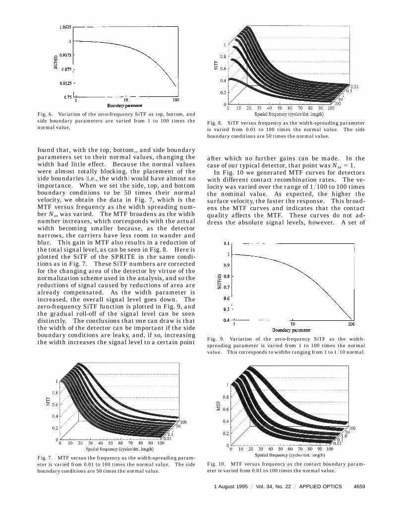
found that, with the top, bottom,, and side boundaryparameters set to their normal values, changing thewidth had little effect. Because the normal valueswere almost totally blocking, the placement of theside boundaries 1i.e., the width2 would have almost noimportance. When we set the side, top, and bottomboundary conditions to be 50 times their normalvelocity, we obtain the data in Fig. 7, which is theMTF versus frequency as the width spreading num-ber Nsx was varied. The MTF broadens as the widthnumber increases, which corresponds with the actualwidth becoming smaller because, as the detectornarrows, the carriers have less room to wander andblur. This gain in MTF also results in a reduction ofthe total signal level, as can be seen in Fig. 8. Here isplotted the SiTF of the SPRITE in the same condi-tions as in Fig. 7. These SiTF numbers are correctedfor the changing area of the detector by virtue of thenormalization scheme used in the analysis, and so thereductions of signal caused by reductions of area arealready compensated. As the width parameter isincreased, the overall signal level goes down. Thezero-frequency SiTF function is plotted in Fig. 9, andthe gradual roll-off of the signal level can be seendistinctly. The conclusions that one can draw is thatthe width of the detector can be important if the sideboundary conditions are leaky, and, if so, increasingthe width increases the signal level to a certain point
Fig. 6. Variation of the zero-frequency SiTF as top, bottom, andside boundary parameters are varied from 1 to 100 times thenormal value.
Fig. 7. MTF versus the frequency as the width-spreading param-eter is varied from 0.01 to 100 times the normal value. The sideboundary conditions are 50 times the normal value.
after which no further gains can be made. In thecase of our typical detector, that point wasNsx 5 1.In Fig. 10 we generated MTF curves for detectors
with different contact recombination rates. The ve-locity was varied over the range of 1@100 to 100 timesthe nominal value. As expected, the higher thesurface velocity, the faster the response. This broad-ens the MTF curves and indicates that the contactquality affects the MTF. These curves do not ad-dress the absolute signal levels, however. A set of
Fig. 8. SiTF versus frequency as the width-spreading parameteris varied from 0.01 to 100 times the normal value. The sideboundary conditions are 50 times the normal value.
Fig. 9. Variation of the zero-frequency SiTF as the width-spreading parameter is varied from 1 to 100 times the normalvalue. This corresponds to widths ranging from 1 to 1@10 normal.
Fig. 10. MTF versus frequency as the contact boundary param-eter is varied from 0.01 to 100 times the normal value.
1 August 1995 @ Vol. 34, No. 22 @ APPLIED OPTICS 4659

SiTF curves, each normalized by the same normaliza-tion constant, is shown in Fig. 11. The boundarynumber here varies between 1@100 and 1 times thenominal value. These graphs show that for low orhigh values of contact velocity, the response is reduced.This reduction is so great that it swamps the broaden-ing of the MTF at high surface velocities.This counterintuitive finding, that better contacts
actually produce worse performance, can be explainedby looking at the effect of boundary condition on themodes. The two extreme cases of ohmic contactsand blocking contacts are shown in Fig. 12. Thefigure shows a typical mode profile in the two cases atthe readout end of the SPRITE detector with thereadout region demarcated. The signal is related tothe total charge inside the readout zone, and this issignified by the shaded areas. In the case of ohmiccontacts, all the modes of charge distribution have azero at the end of the detector. This reduces theamount of charge in the readout, as shown by thesmaller shaded area. In the case of perfectly block-ing contacts, all the modes have their maximum atthe end of the detector, which results in a relativelylarge amount of charge in the readout, as demon-strated by the larger shaded area. This is whatcauses the increase of signal for partially blockingcontacts and the reduction of signal for ohmic con-tacts.
Fig. 11. SiTF versus frequency as the contact boundary param-eter is varied from 1 to 0.01.
Fig. 12. Diagram of the charge distribution in the SPRITE inohmic and blocking boundary conditions. The shaded regionsrepresent the readout charge.
4660 APPLIED OPTICS @ Vol. 34, No. 22 @ 1 August 1995
Because SiTF performance degrades as the contactconditions become either too high or too low, it standsto reason that an optimum value exists between thesetwo extremes. This optimum can be seen in Fig. 13,where the SiTF at zero frequency is shown as afunction of the boundary parameter. This figureclearly illustrates that the signal strength goesthrough a maximum when the contact boundaryparameter is approximately 0.50. This correspondsto a surface recombination velocity, for our typicaldetector, of 40 cm@s. If possible, such tailoring of thecontact velocity of SPRITE detectors could result inlarge increases in their signal-level performance.
5. Conclusions
In this paper we have presented a new solution to theproblem of carrier-transport dynamics in SPRITEdetectors through the use of eigenmodal analysis.In doing so, we developed a self-consistent model forthe detector. This model and method intrinsicallyinclude boundary conditions and full dimensionalityand thus are more complete. Through the analysis,certain dimensionless numbers arise that can be usedto characterize SPRITE structure parameters andclarify how these parameters affect device perfor-mance. Expressions for the MTF have been derived,and various representative computed functions arepresented. From these curves, optimum values forthe insulating and contact boundary numbers havebeen determined.
This work was supported by Westinghouse ElectricCorporation, Orlando, Fla.
References1. C. T. Elliot, ‘‘Thermal imaging systems,’’ U.S. patent 3,995,159,
130 Nov. 19762.2. C. T. Elliot, ‘‘New detector for thermal imaging systems,’’
Electron. Lett. 17, 312–313 119812.3. D. J. Day and T. J. Shepherd, ‘‘Transport in photoconductors—
I,’’ Solid State Electron. 25, 707–712 119822.
Fig. 13. Zero-frequency SiTF versus the contact boundary param-eter. The optimum value of the boundary parameter is around0.5.

4. T. J. Shepherd and D. J. Day, ‘‘Transport in photoconductors—II,’’ Solid State Electron. 25, 713–718 119822.
5. G. D. Boreman and A. E. Plogstedt, ‘‘Modulation transferfunction and number of equivalent elements for SPRITEdetectors,’’ Appl. Opt. 27, 4331–4335 119882.
6. S. P. Braim andA. P. Campbell, ‘‘TED 1SPRITE2 detector MTF,’’Inst. Electr. Eng. Conf. 228, 63–66 119832.
7. T. Ashley and C. T. Elliot, ‘‘Accumulation effects at contacts ton-type cadmium mercury telluride photoconductors,’’ InfraredPhys. 22, 367–376 119822.
8. M. Boas, Mathematical Methods in the Physical Sciences1Wiley, NewYork, 19832, p. 541.
9. T. Ashley, C. T. Elliott, A. M. White, J. T. M. Wotherspoon, and
M. D. Johns, ‘‘Optimization of spatial resolution in SPRITEdetectors,’’ Infrared Phys. 24, 25–33 119842.
10. J. A. Whitlock, G. D. Boreman, H. K. Brown, and A. E.Plogstedt, ‘‘Electrical network model for SPRITE detectors,’’Opt. Eng. 30, 1784–1787 119912.
11. S. M. Sze, Physics of Semiconductor Devices 1Interscience, NewYork, 19692, p. 71.
12. E. Buckingham, ‘‘On physically similar systems; illustrationsof the use of dimensional analysis,’’ Phys. Rev. 4, 345–376119142.
13. G. D. Boreman and A. E. Plogstedt, ‘‘Spatial filtering by aline-scanned nonrectangular detector: application to SPRITEreadout MTF,’’ Appl. Opt. 28, 1165–1168 119892.
1 August 1995 @ Vol. 34, No. 22 @ APPLIED OPTICS 4661