MINIMUM USAGE OF FERRITE TILES IN ANECHOIC CHAMBERS · PDF fileMINIMUM USAGE OF FERRITE TILES...
17
Progress In Electromagnetics Research B, Vol. 19, 367–383, 2010 MINIMUM USAGE OF FERRITE TILES IN ANECHOIC CHAMBERS S. M. J. Razavi, M. Khalaj-Amirhosseini, and A. Cheldavi College of Electrical Engineering Iran University of Science and Technology Tehran, Iran Abstract—Anechoic chambers which are used for emission and immunity testing require expensive ferrite tiles on their inner surfaces. This paper describes a method to reduce the number of required ferrite tiles, whilst ensuring a reliable and specified test region. In this method, the positions of some ferrite tiles are found optimally to keep the performance of the anechoic chamber as high as possible. An optimum ray-tracing method is presented to predict the electric field in the anechoic chamber. The performance of the proposed method is verified by a comprehensive example simulated by the CST software, which is a full-wave simulator based on time difference method. 1. INTRODUCTION The need for indoor testing of electromagnetic radiating devices, which began in the early 1950s [1], has led to a number of companies providing chambers and absorber products supporting a range of electromagnetic testing requirements. Microwave anechoic chambers are currently in use for a variety of indoor antenna measurements, electromagnetic interference (EMI) measurements, and electromagnetic compatibility (EMC) measurements. The anechoic chamber provides a test volume, called the “quiet zone”, in which the level of reflected waves determines the performance of the anechoic chamber. Some series of materials have been developed for absorption in the 30 to 1000 MHz frequency range. The most common material is ferrite tile. Ferrite tiles are expensive, and the room strength required to support the weight of the tiles (of the order of 30 kg/m 2 ) adds to the cost. The need for decreasing the cost led to the development of some optimized analytical and practical methods. Based on experiments [2], Corresponding author: S. M. J. Razavi ([email protected]).
-
Upload
nguyenminh -
Category
Documents
-
view
219 -
download
5
Transcript of MINIMUM USAGE OF FERRITE TILES IN ANECHOIC CHAMBERS · PDF fileMINIMUM USAGE OF FERRITE TILES...

Progress In Electromagnetics Research B, Vol. 19, 367–383, 2010
MINIMUM USAGE OF FERRITE TILES IN ANECHOICCHAMBERS
S. M. J. Razavi, M. Khalaj-Amirhosseini, and A. Cheldavi
College of Electrical EngineeringIran University of Science and TechnologyTehran, Iran
Abstract—Anechoic chambers which are used for emission andimmunity testing require expensive ferrite tiles on their inner surfaces.This paper describes a method to reduce the number of requiredferrite tiles, whilst ensuring a reliable and specified test region. Inthis method, the positions of some ferrite tiles are found optimally tokeep the performance of the anechoic chamber as high as possible. Anoptimum ray-tracing method is presented to predict the electric fieldin the anechoic chamber. The performance of the proposed method isverified by a comprehensive example simulated by the CST software,which is a full-wave simulator based on time difference method.
1. INTRODUCTION
The need for indoor testing of electromagnetic radiating devices, whichbegan in the early 1950s [1], has led to a number of companies providingchambers and absorber products supporting a range of electromagnetictesting requirements. Microwave anechoic chambers are currently inuse for a variety of indoor antenna measurements, electromagneticinterference (EMI) measurements, and electromagnetic compatibility(EMC) measurements. The anechoic chamber provides a test volume,called the “quiet zone”, in which the level of reflected waves determinesthe performance of the anechoic chamber.
Some series of materials have been developed for absorption inthe 30 to 1000MHz frequency range. The most common material isferrite tile. Ferrite tiles are expensive, and the room strength requiredto support the weight of the tiles (of the order of 30 kg/m2) adds to thecost. The need for decreasing the cost led to the development of someoptimized analytical and practical methods. Based on experiments [2],
Corresponding author: S. M. J. Razavi ([email protected]).

368 Razavi, Khalaj-Amirhosseini, and Cheldavi
with 80% of the Fresnel zone [3] covered for absorption the variationof the E-field is very uniform at all frequencies above 300 MHz, andthe maximum error is approximately 1.4 dB. It is possible to cover just80% of the surface of the chamber with ferrite absorber and obtain aresponse which is within ±4 dB of the free space response between 40and 200 MHz [4]. Some other optimization methods using additionalabsorbers, shifted absorbers, and optimized absorbers are proposedin [5].
In this paper, a new method is proposed to reduce the need forfull coverage using ferrite tiles and to optimize the layout of ferrite tilesto reach good performance and minimize cost. The proposed methodhas been simulated via computer programs and is validated with theCST software.
The modeling technique is described in Section 2. Section 3presents an example and the results of the work. Conclusions aregiven in Section 4.
2. MODELING TECHNIQUE
In the first step, the electric field in the anechoic chamber is evaluatedfor a dipole antenna using the optimum ray-tracing method, describedin Section 2.1. The next step explains the proposed algorithm,described in Section 2.2, to determine the layout of ferrite tiles inthe inner surfaces of the chamber to produce the best performance.The model of a ferrite tile over a wide frequency range is described inSection 2.3.
2.1. Optimum Ray-tracing Method
The known ray tracing technique which is based on geometrical optics(GO) provides a relatively simple solution for indoor wave propagation.It should be noted that using the GO and ray tracing technique isvalid only when the object of interest has dimensions greater than thewavelength.
In the ray tracing method, the waves radiated from a transmittingantenna can be modeled as many ray tubes shooting from the locationof the antenna [6, 7]. In a ray-tracing program, each ray tube maybe composed of four rays separated by the increments of θ and ϕ(∆θ and ∆ϕ) in local spherical coordinates, centered at the antenna.To generate the ray tubes, a sphere of radius r centered at theantenna is divided into quadrilateral cells that are close to squareswith approximately the same area by selecting a fixed ∆θ and a

Progress In Electromagnetics Research B, Vol. 19, 2010 369
∆ϕ = ∆θ/ sin θ. Fig. 1 shows the simulated region that is an anechoicchamber with six boundary surfaces.
In the conventional ray-tracing procedure, the rays have beentraced one by one [6–8, 14, 15], taking a large run time. To speed up theray tracing algorithm, we propose to trace the rays simultaneously. Inthis way, the ray-tracing procedure may be modified by the followingtwo steps:
1) The boundary surfaces intersected with all rays have to be foundat one time. Consider one of the boundary surfaces with arectangular shape as shown in Fig. 2 whose normal unit vectoris ni. One plane (oajaj+1), in which j = 1, 2, 3, 4, o is the pointsource and ajs are the edge points of the boundary surface, ispassed through each side of this boundary surface (ajaj+1) andthe point source. The normal unit vector of each defined planecan be determined from the following expression:
_nij =
−→oaj ×−−−→oaj+1
|−→oaj ×−−−→oaj+1| (1)
In (1), if j + 1 becomes greater than 4, it is replaced by 1.A function f is defined such that it takes 1 for the rays incidentto the boundary surface No. i and takes zero for the other rays.
f (i, r) = 1 + sign
4∑
j=1
sign (nij · r)− 4
(2)
where r is directional vector of the incident ray and sign is thesign function.
O
3a
1a
2a
4a
5a
6a
7a
8a
Figure 1. Geometry of ananechoic chamber.
4a
o
1a
2a
3a
in
).(.. iNoSB
Figure 2. Boundary surfacenumber i; i = 1, 2, 3, 4, 5, 6 andsource point.
370 Razavi, Khalaj-Amirhosseini, and Cheldavi
2) The sum of the products of defined functions f and the normalunit vectors ni give us the normal unit vector of the correspondingboundary surfaces of all rays, at one time, as the following relation:
n =6∑
i=1
f (i, r) · ni (3)
Also, an arbitrary point of corresponding boundary surfaces of allrays can be found using a similar expression as follows:
P =6∑
i=1
f (i, r) · Pi (4)
where Pi is an arbitrary point on the intersecting boundarysurfaces No. i.
The other steps are similar to the known ray-tracing algorithmproposed in [8]. It is worth mentioning that the proposed ray tracingalgorithm could be useful in numerical software, such as MATLABwhich based on matrix operations.
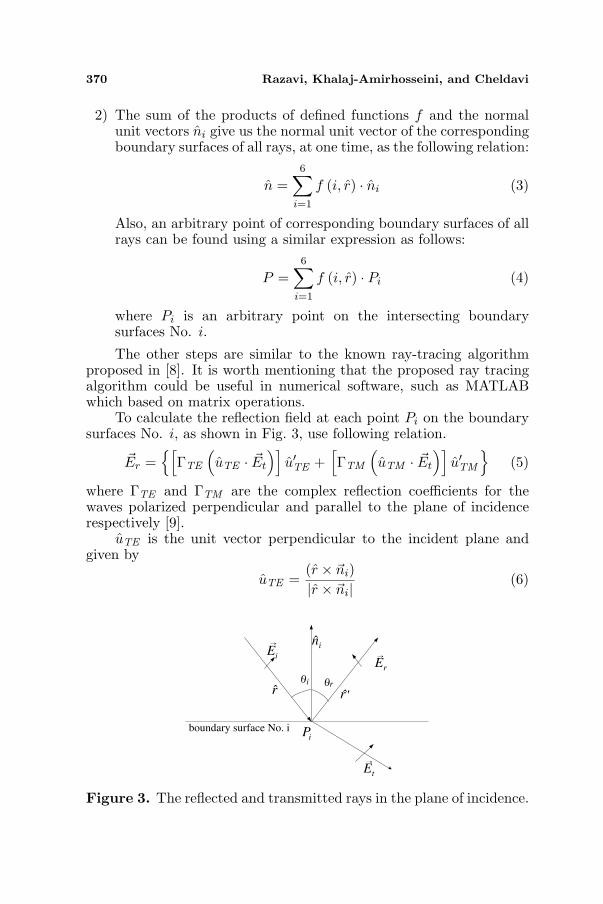
To calculate the reflection field at each point Pi on the boundarysurfaces No. i, as shown in Fig. 3, use following relation.
~Er ={[
ΓTE
(uTE · ~Et
)]u′TE +
[ΓTM
(uTM · ~Et
)]u′TM
}(5)
where ΓTE and ΓTM are the complex reflection coefficients for thewaves polarized perpendicular and parallel to the plane of incidencerespectively [9].
uTE is the unit vector perpendicular to the incident plane andgiven by
uTE =(r × ~ni)|r × ~ni| (6)
iE
rE
tE
in
i r
r r'
iP
θ θ
→
→
→
boundary surface No. i
Figure 3. The reflected and transmitted rays in the plane of incidence.
Progress In Electromagnetics Research B, Vol. 19, 2010 371
where r is unit vector along incident ray and the reflected ray along r′also lies in the same incident plane, i.e.,
u′TE = uTE (7)
uTM is a unit vector parallel to the plane of incidence and alsoperpendicular to the direction
~uTM =(r × uTE )|r × uTE | (8)
For the reflected ray the corresponding unit vector is given as
u′TM = −(r′ × uTE )|r′ × uTE | (9)
2.2. Optimized Algorithm for Setting Absorber Material
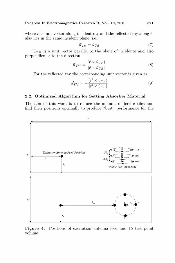
The aim of this work is to reduce the amount of ferrite tiles andfind their positions optimally to produce “best” performance for the
TOP
MID
LOW
12
34 5
67
89 10
1112
13
14 15
2
3
4 51
l
haz
ay
ax
aqlw
qr
qh5.
qh5.
)zonequiet (TestVolume
PositionFeedAntennaExcitation
Figure 4. Positions of excitation antenna feed and 15 test pointvolume.

372 Razavi, Khalaj-Amirhosseini, and Cheldavi
anechoic chamber. For this purpose, 15 points of the quiet zone wereselected as the test points. Fig. 4 shows the top-view and side-view ofthe anechoic chamber along with the positions of the feed of excitationantenna and the test points.
The proposed optimization algorithm is based on the followingfive steps:
1) The inner surface of the chamber is meshed by using a rectangulargrid with square cells of the size ∆l×∆l, where ∆l represents theresolution factor of the analysis method.
2) A cost matrix with initial zero value is defined and assigned forthis grid, so that each element of the matrix corresponds to theone cell of the grid.
3) In each iteration, the cells that ray tubes strike before passing fromthe test points are found. An instantaneous cost matrix with thevalue of one for these cells and zero for the other cells is defined.
4) The defined cost matrix is updated by the following equation inthe ith iteration:
cost matrix (i)=cost matrix (i−1)+(inst cost matrix (i)/i) (10)
5) The optimization process will be terminated if the magnitude ofthe all E-fields is less than a threshold.
At the end of the optimization process, the cost matrix is obtainedso that the important cells have higher values than the other ones. Toreduce the need for full coverage using ferrite tiles and to minimizethe cost, the cells with low values in the cost matrix are not coveredwith ferrite tiles. It is done considering the desired coverage percentof ferrite tiles. The above discussion has been quantified in the resultssection.
The proposed optimization algorithm is simple and about 24 timesfaster than the conventional methods such as a genetic algorithm [8];for example in a special case the run of the proposed method tookabout 30 minutes on a normal PC while it took more than 12 hoursfor the genetic algorithm.
2.3. Representing Ferrite Tiles
Ferrite tiles are made of solid ferrite of about 6 mm thickness or ina grid construction of approximately 20 mm thickness. The frequencyresponse of these ferrite tiles cannot be modeled accurately over a widefrequency range [16]. This is due to the change in their permeabilitywith frequency. To consider frequency-dependent material behavior inbroadband simulations, the most common models up to second-order

Progress In Electromagnetics Research B, Vol. 19, 2010 373
dispersions are available [10, 11]. These models include relaxation andresonance effects as well as plasma or even gyrotropic media.
The relaxation process, also called first-order Debye model ischaracterized by the following formulation for the relative permeability,containing the relaxation time τ , infinity permeability µ∞ and staticpermeability µs [10, 11].
µ (ω) = µ∞ +µs − µ∞1 + jωτ
(11)
Figure 5 shows the real and imaginary parts of the relativepermeability of one of the commercial ferrite tile absorbers and theirsimulation models. For this type of ferrite τ = 33.22 ns, µ∞ = µ0
and µs = 1394.5µ0 where µ0 is the vacuum permeability. The relativepermittivity of this compound is approximately equal to 11.
When a ray tube is incident on the ferrite tile, a reflected anda transmitted ray tube is generated according to Snell’s law andthe local plane wave approximation. The reflection and transmissioncoefficients of the TE and TM plane wave illuminating a flat interfaceof two materials are employed in all text books such as [9]. In theelectromagnetic anechoic chamber, the back of ferrite tiles is a perfectelectric conductor, which has been considered in simulation.
Figure 5. Relative permeability of a ferrite tile.
374 Razavi, Khalaj-Amirhosseini, and Cheldavi
3. RESULTS
The proposed method is applied to optimize a practical anechoicchamber such as EMC test chamber compact TC800-20 [12].
The characteristics of this chamber are listed in Table 1. Theexcitation antenna feed position is (xa, ya, za) = (1.5, 1, 2)m and theother parameters shown in Fig. 4 are hq = 1m, rq = .75 m andlaq = 2.25m. As previously explained in Section 2.2, the elementsof the cost matrix are assigned high values for the important cells andlow values for the non important cells, and then the ferrite tiles are usedonly in the important cells of the inner surface of the anechoic chamber.For this purpose the high value elements of the cost matrix have beenspecified by a suitable threshold level. For testing and validating thelayout of ferrite tiles, the field uniformity of anechoic chamber has beencalculated by CST software.
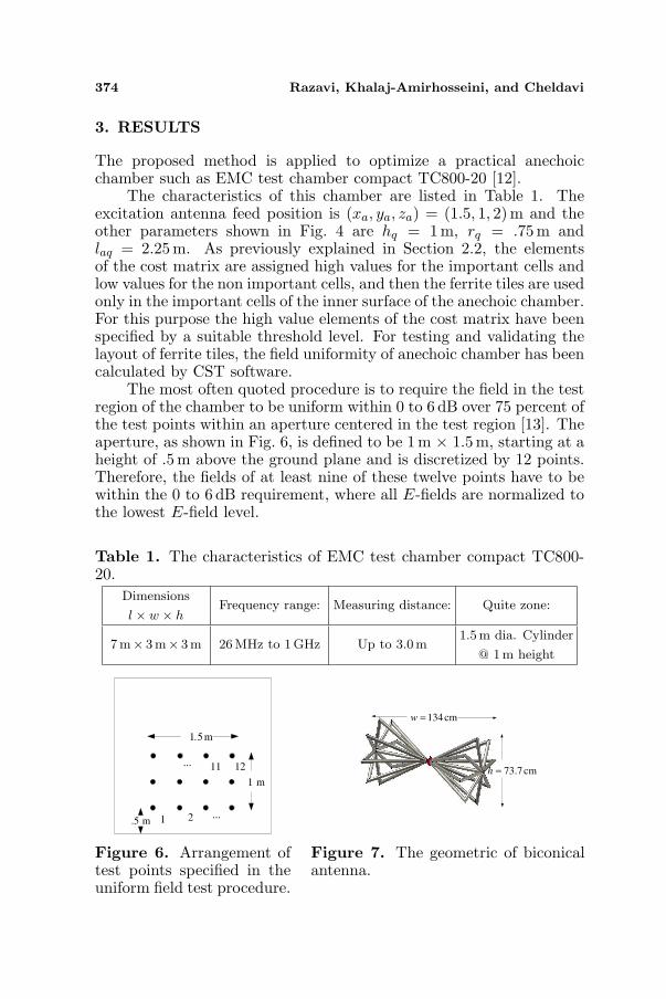
The most often quoted procedure is to require the field in the testregion of the chamber to be uniform within 0 to 6 dB over 75 percent ofthe test points within an aperture centered in the test region [13]. Theaperture, as shown in Fig. 6, is defined to be 1m × 1.5m, starting at aheight of .5m above the ground plane and is discretized by 12 points.Therefore, the fields of at least nine of these twelve points have to bewithin the 0 to 6 dB requirement, where all E-fields are normalized tothe lowest E-field level.
Table 1. The characteristics of EMC test chamber compact TC800-20.
Dimensions
l × w × hFrequency range: Measuring distance: Quite zone:
7m× 3m× 3m 26MHz to 1GHz Up to 3.0 m1.5m dia. Cylinder
@ 1m height
m5.1
m1
21
1211
...
...
m5.
Figure 6. Arrangement oftest points specified in theuniform field test procedure.
cmw 134=
cmh 7.73=
Figure 7. The geometric of biconicalantenna.
Progress In Electromagnetics Research B, Vol. 19, 2010 375
The results of this work are explained in the following subsections.
3.1. Excitation Antenna
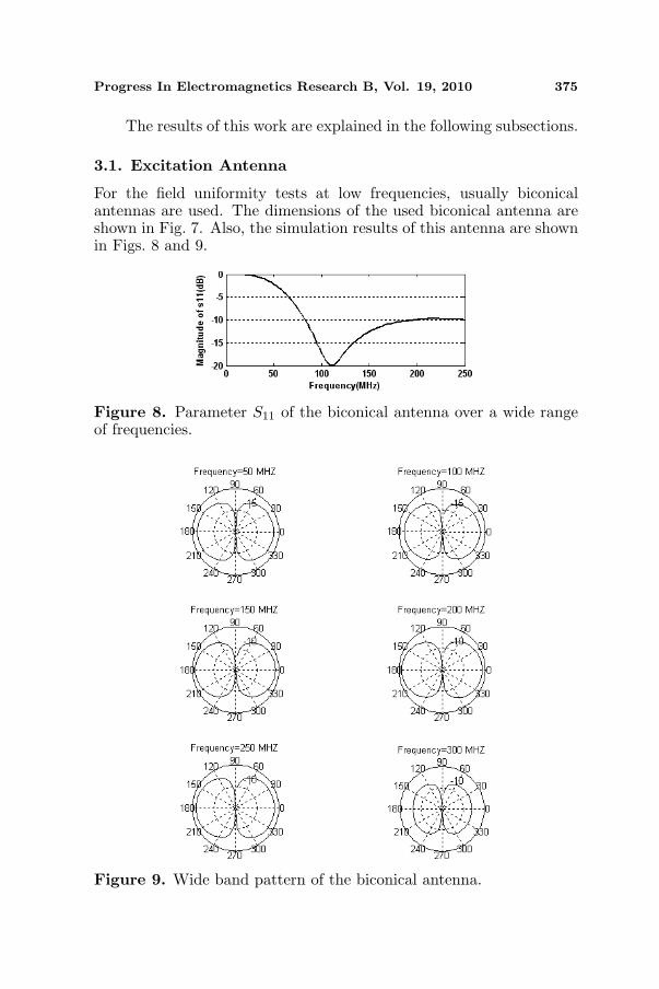
For the field uniformity tests at low frequencies, usually biconicalantennas are used. The dimensions of the used biconical antenna areshown in Fig. 7. Also, the simulation results of this antenna are shownin Figs. 8 and 9.
Figure 8. Parameter S11 of the biconical antenna over a wide rangeof frequencies.
Figure 9. Wide band pattern of the biconical antenna.

376 Razavi, Khalaj-Amirhosseini, and Cheldavi
3.2. 90% and 85% Coverage of Ferrite Tiles
The inner surface of the anechoic chamber is meshed by using arectangular grid with square cells of the size 20 cm. In the first example,90% of the inner surface of the anechoic chamber which has a high valuein the cost matrix is covered by ferrite tiles. The obtained layout offerrite tiles is shown in Fig. 10. Nearly all of the cells of the back andfront walls are found to be important and therefore have to be coveredby ferrite tiles.
Figure 11 shows the parameter S11 of the excitation antenna,which is acceptable compared with Fig. 8. Also, the relative levelsof the E-fields are within an acceptable range (0 to 6 dB) for most ofthe twelve test points as shown in Fig. 12.
Figure 10. Optimized layout of ferrite tiles for 90% coverage of theinner surface of the anechoic chamber (black=tiles, white=no tiles).
Figure 11. Parameter S11 of the excitation antenna in the anechoicchamber with 90% coverage of ferrite tiles.

Progress In Electromagnetics Research B, Vol. 19, 2010 377
Figure 12. Field uniformity test result in the anechoic chamber withwith 90% coverage of ferrite tiles.
Figure 13. Optimized layout of ferrite tiles for 85% coverage of theinner surface of the anechoic chamber (black=tiles, white=no tiles).
In the second example, 85% of the inner surface of the anechoicchamber which has a high value in the cost matrix is covered by ferritetiles. The obtained results of this example are shown in Figs. 13, 14,and 15. Again, it is seen that the results are acceptable.

378 Razavi, Khalaj-Amirhosseini, and Cheldavi
Figure 14. Parameter S11 of the excitation antenna in the anechoicchamber with 85% coverage of ferrite tiles.
Figure 15. Field uniformity test results in the anechoic chamber with85% coverage of ferrite tiles.
3.3. 80% Coverage of Ferrite Tiles
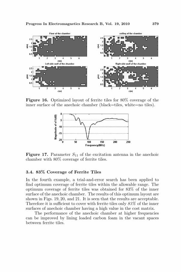
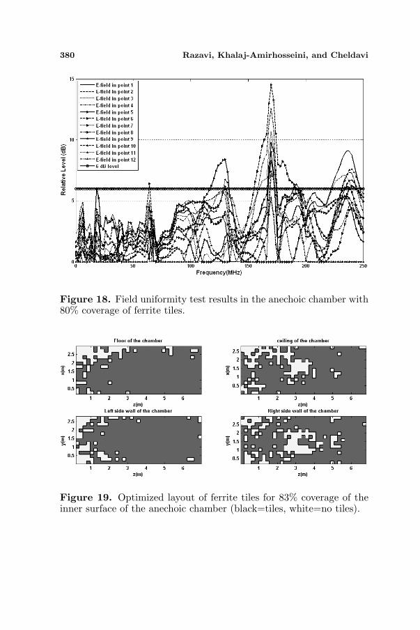
In the third example, 80% of the inner surface of anechoic chamberwhich has a high value in the cost matrix is covered by ferrite tiles. Theobtained results of this example are shown in Figs. 16, 17, and 18. It isseen that the results are not acceptable, because the field uniformityand the parameter S11 of the excitation antenna are poor. Now, onemay be conclude that the optimum coverage of ferrite tiles is between80–85% of the inner surface of the anechoic chamber.
Progress In Electromagnetics Research B, Vol. 19, 2010 379
Figure 16. Optimized layout of ferrite tiles for 80% coverage of theinner surface of the anechoic chamber (black=tiles, white=no tiles).
Figure 17. Parameter S11 of the excitation antenna in the anechoicchamber with 80% coverage of ferrite tiles.
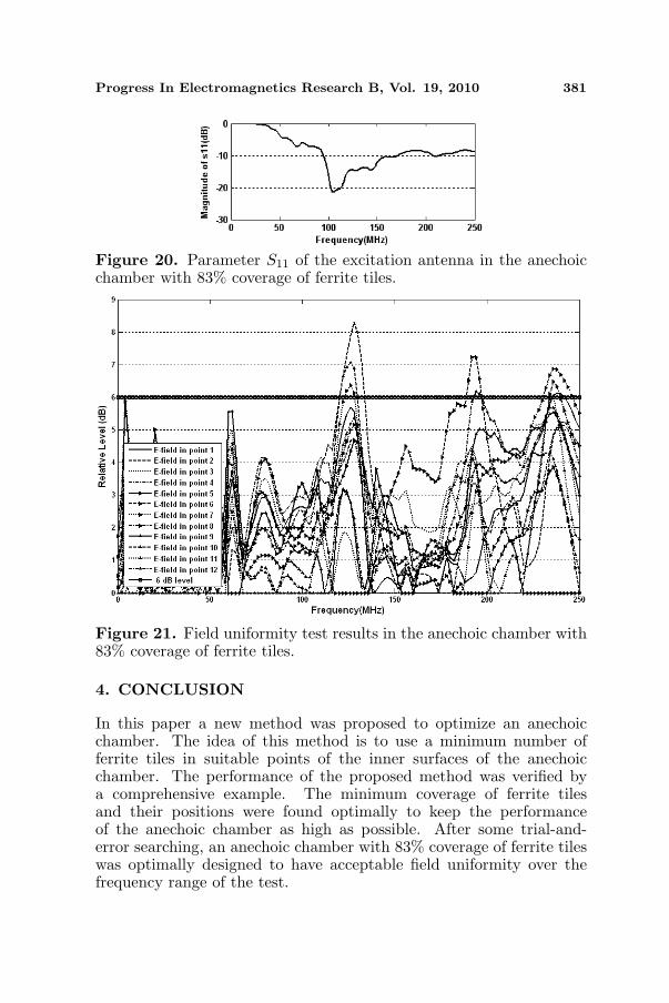
3.4. 83% Coverage of Ferrite Tiles
In the fourth example, a trial-and-error search has been applied tofind optimum coverage of ferrite tiles within the allowable range. Theoptimum coverage of ferrite tiles was obtained for 83% of the innersurface of the anechoic chamber. The results of this optimum layout areshown in Figs. 19, 20, and 21. It is seen that the results are acceptable.Therefore it is sufficient to cover with ferrite tiles only 83% of the innersurfaces of anechoic chamber having a high value in the cost matrix.
The performance of the anechoic chamber at higher frequenciescan be improved by lining loaded carbon foam in the vacant spacesbetween ferrite tiles.
380 Razavi, Khalaj-Amirhosseini, and Cheldavi
Figure 18. Field uniformity test results in the anechoic chamber with80% coverage of ferrite tiles.
Figure 19. Optimized layout of ferrite tiles for 83% coverage of theinner surface of the anechoic chamber (black=tiles, white=no tiles).
Progress In Electromagnetics Research B, Vol. 19, 2010 381
Figure 20. Parameter S11 of the excitation antenna in the anechoicchamber with 83% coverage of ferrite tiles.
Figure 21. Field uniformity test results in the anechoic chamber with83% coverage of ferrite tiles.
4. CONCLUSION
In this paper a new method was proposed to optimize an anechoicchamber. The idea of this method is to use a minimum number offerrite tiles in suitable points of the inner surfaces of the anechoicchamber. The performance of the proposed method was verified bya comprehensive example. The minimum coverage of ferrite tilesand their positions were found optimally to keep the performanceof the anechoic chamber as high as possible. After some trial-and-error searching, an anechoic chamber with 83% coverage of ferrite tileswas optimally designed to have acceptable field uniformity over thefrequency range of the test.
382 Razavi, Khalaj-Amirhosseini, and Cheldavi
REFERENCES
1. Emerson, W. H., “Electromagnetic wave absorbers and anechoicchambers through the years,” IEEE Trans. on Ant. and Propag.,Vol. 21, No. 4, Jul. 1973.
2. Kineros, C. and V. Ungvichian, “A low cost conversion of semi-anechoic chamber to fully anechoic chamber for RF antennameasurements,” IEEE International Symposium on Electromag.Compat., Vol. 2, 724–729, Aug. 2003.
3. Collin, R. E., Antennas and Radio Wave Propagation, McGrawHill, 1985.
4. Dawson, L., J. Clegg, S. J. Porter, J. F. Dawson, andM. J. Alexander, “The use of genetic algorithms to maximizethe performance of a partially lined screened room,” IEEE Trans.Electromagn. Compat., Vol. 44, No. 1, 233–242, Feb. 2002.
5. Bornkessel, C. and W. Wiesbeck, “Numerical analysis andoptimization of anechoic chambers for EMC testing,” IEEE Trans.Electromagn. Compat., Vol. 38, No. 3, 499–506, Aug. 1996.
6. Yang, C. F., B. C. Wu, and C. J. Ko, “A ray-tracing method formodeling indoor wave propagation and penetration,” IEEE Trans.on Ant. and Propag., Vol. 46, No. 6, 907–919, Jun. 1998.
7. Kim, H. and H. Ling, “Electromagnetic scattering from aninhomogeneous object by ray tracing,” IEEE Trans. on Ant. andPropag., Vol. 40, 517–525, May 1992.
8. Razavi, S. M. J. and M. Khalaj-Amirhosseini, “Optimization ofan anechoic chamber with ray-tracing and genetic algorithms,”Progress In Electromagnetics Research B, Vol. 9, 53–68, 2008.
9. Balanis, C. A., Advanced Engineering Electromagnetics, JohnWiley & Sons, 1989.
10. Qi, X., J. Zhou, Z. Yue, Z. Gui, L. Li, and S. Buddhudu,“A ferroelectric ferromagnetic composite material with significantpermeability and permittivity,” Advanced Functional Materials,Vol. 14, No. 9, 920–926, Sept. 2004.
11. Wu, J., M. Y. Koledintseva, and J. L. Drewniak, “FDTD modelingof structures containing dispersive isotropic magnetic materials,”Proc. IEEE Int. Symp. Electromagn. Compat., Vol. 2, 904–909,Boston, Aug. 18–22, 2003.
12. www.rfi-ind.com.au/download/Compact%20TC800-20.pdf.13. CENELEC EN 61000-4-3: 1996, Electromagnetic Compatibility
(EMC)-Part 4-3: Testing and Measurement Techniques-Radiated,Radio-Frequency, Electromagnetic Field Immunity Test.
Progress In Electromagnetics Research B, Vol. 19, 2010 383
14. Kim, H. and H.-S. Lee, “Accelerated three dimensional ray tracingtechniques using ray frustums for wireless propagation models,”Progress In Electromagnetics Research, PIER 96, 21–36, 2009.
15. Tayebi, A., J. Gomez, F. S. Saez de Adana, and O. Gutierrez,“The application of ray-tracing to mobile localization using thedirection of arrival and received signal strength in multipathindoor environments,” Progress In Electromagnetics Research,PIER 91, 1–15, 2009.
16. Khalaj-Amirhosseini, M. and H. Ghorbaninejad-Foumani, “Tocompact waveguide devices by dielectric and ferrite layers,”Progress In Electromagnetics Research M, Vol. 9, 243–255, 2009.